design standard insulation - jaxasma.jaxa.jp/en/techdoc/docs/e_jaxa-jerg-2-213a-08a_re.pdf ·...
TRANSCRIPT

JERG-2-213A
DESIGN STANDARD
INSULATION
May 10, 2012 Revision A
Japan Aerospace Exploration Agency

JERG-2-213A
i
This is an English translation of JERG-2-213A. Whenever there is anything ambiguous in this document, the original document (the Japanese version) shall be used to clarify the intent of the requirement. Disclaimer The information contained herein is for general informational purposes only. JAXA makes no warranty, express or implied, including as to the accuracy, usefulness or timeliness of any information herein. JAXA will not be liable for any losses relating to the use of the information. Published by Japan Aerospace Exploration Agency Safety and Mission Assurance Department 2-1-1 Sengen Tsukuba-shi,Ibaraki 305-8505, Japan

JERG-2-213A
ii
Contents
1 Scope of application ................................................................................................ 1 1.1 Purpose ............................................................................................................. 1 1.2 Scope of application .......................................................................................... 1
2 References .............................................................................................................. 1 3 Terms ....................................................................................................................... 1 4 General requirements .............................................................................................. 2 5 Design requirements and design methods .............................................................. 3
5.1 Insulation design ............................................................................................... 3 5.1.1 Insulation design using dielectric gas ............................................................. 3 5.1.2 Insulation design using solid dielectrics ......................................................... 5 5.1.3 Creeping insulation design ............................................................................. 9 5.2 Measures with double insulation ....................................................................... 9 5.2.1 Definition of double insulation ........................................................................ 9 5.2.1.1 Space insulation (interconductor insulation) .............................................. 10 5.2.1.2 Solid body insulation .................................................................................. 11 5.2.2 Parts to apply double insulation .................................................................... 11 5.2.3 Implementation example of double insulation .............................................. 12
6. Appendix ............................................................................................................... 13 Appendix I Mechanism of breakdown ....................................................................... 13 I.1 Mechanism of breakdown [1-3] ............................................................................ 13 I.1.1 Conduction of solid body .................................................................................. 13 I.1.2 Breakdown mechanism of solid body ............................................................... 14 I.1.2.1 Electronic breakdown process ....................................................................... 15 I1.2.2 Thermal breakdown process .......................................................................... 19 I1.2.3 Electromechanical breakdown ........................................................................ 22 I1.2.4 Partial discharge ............................................................................................. 24 I1.2.5 Treeing ............................................................................................................ 29 I1.2.6 Tracking .......................................................................................................... 29 I1.3 Creeping discharge mechanism ........................................................................ 30 I1.3.1 Creeping discharge in gaseous phase............................................................ 30 I1.3.2 Creeping discharge in vacuum [4,5] ............................................................... 32 I1.3.3 Discharge on surface ...................................................................................... 35 I1.3.4 Influence of charging on breakdown ............................................................... 36 Appendix II Influence of concentrating electric field and electron emission from electrode material ..................................................................................................... 39 II1 Relation between electrode shape and electric field [1] ....................................... 39 II2 Electrode material and electron emission ............................................................ 41 II3 Influence of work function in metals ..................................................................... 43 II4 Surface treatment of electrode ............................................................................ 43 Appendix III Influence of neutral molecular on discharging ...................................... 45 III1 Paschen’s law in gas [1,3] .................................................................................. 45 III2 Issues and measures on hot launch ................................................................... 47 Appendix IV Creeping distance and discharge voltage ............................................ 49 IV1 Creeping distance and discharge voltage [1] ..................................................... 49 IV2 Concept of preventing creeping surface discharge ............................................ 52

JERG-2-213A
1
1 Scope of application
1.1 Purpose
The insulation design standard (referred to as “this standard” in this document)
specifies fundamental requirements about power supply system insulation design
of spacecraft developed by the Japan Aerospace Exploration Agency (referred to
as “JAXA” in this document).
The appendices summarize the explanation of causes for breakdown and
information required to utilize this standard.
1.2 Scope of application
This standard is applicable as a design standard insulation design for the power
supply system up to a nominal voltage of 100V for spacecraft developed by
JAXA.
The insulation design of printed circuit boards shall be compliant with other
JAXA's printed circuit board design standard and shall not applicable to this
design standard.
This standard assumes that project-specific specifications should be defined if
there are parts which have difficulty in conforming to this standard, provided that
the reasons for the difficulties are clearly presented.
2 References
This standard was created with reference to the following documents:
(1) IEC document
IEC-J60950 Safety standard of information technology devices
(2) Japanese Industrial Standards
JIS C 0704 Insulation distance, insulation resistance and withstand voltage of
control device
JIS C 2110 Dielectric strength test method of solid electric insulation material
3 Terms
(1) Primary power supply
A power source which is generated/controlled by the power system (solar
panel system and power supply system) of an aerospace vehicle, and
commonly distributed to devices loaded in the aerospace vehicle.

JERG-2-213A
2
(2) Primary power supply bus line
A bus line which distributes and supplies the primary power supply.
Applicable bounds are those which have the same potential as the primary
power supply input of loaded devices.
(3) Creeping surface discharge
Discharge that occurs on the boundary surface between different dielectrics.
(4) Conditioning
A process in manufacturing electrode structure, which removes projections
on an electrode, adherences and micro particles on an electrode. There are
methods such as current conditioning, glow discharge conditioning, and
spark conditioning.
(5) Paschen’s law
Under a constant temperature of a gas, in a uniform electric field, a voltage
that generates sparking (Vs: Spark Voltage) is a function of product pd (gas
pressure (p) and gap length (d) ). This is called Paschen’s law, because
Paschen discovered this relationship based on this experiment.
4 General requirements
Various types of insulation materials are used in electronic devices and components
on an aircraft, contributing to maintaining reliability of the aircraft under severe space
environments. On the other hand, if a breakdown of insulation material occurs, it
may cause serious damage to an aircraft. Therefore, it is required to conduct an
insulation design with an understanding of insulation characteristics and breakdown
phenomenon of the insulation materials.
(1) A distance between conductors shall be a level that does not cause a
breakdown in the ground, lift-off and orbit operating environments. In
particular, under lift-off conditions, exposure to significant change of
atmospheric pressure causes a drop of neutral gas particle density between
conductors. Insulation design requires paying attention to a breakdown
under the Paschen’s law.
(2) The distance between conductors shall be specified to be a level that does
not cause a breakdown at the maximum operating voltage that can occur
between conductors.
(3) The insulation design shall also include a specified interconductor distance
by providing clearance in processing and assembling. This shall prevent

JERG-2-213A
3
fluctuation and deformation for operating conditions on the ground, during lift-
off, and in orbit, or shall account for the required distance after fluctuation or
deformation.
(4) In many cases, insulation materials are mounted by applying significant
pressure. They shall be mounted so as to avoid damage and cracks.
(5) Discharge voltages (breakdown voltages) depend on the shape of a
conductor. A radius of curvature at the tip of a conductor shall be as large
as possible, and avoid making sharp edges on a conductor surface where
possible.
(6) Solid dielectrics may cause a drop of breakdown voltage under some
conditions of use. Therefore, a thickness of solid dielectrics shall be
specified in full consideration of derating in accordance with material
characteristics and conditions of use.
(7) To prevent a drop in breakdown voltage caused by gas generated in the
space, the insulation design shall avoid closed spaces between conductors
where possible by taking actions such as providing a vent hole. When using
insulation material made of hardened resin, bubbles and gases in the
material must be completely removed in order to prevent the creation of a
void.
(8) To prevent a breakdown caused by creeping discharge, barriers of pits and
projections shall be provided on solid dielectrics surface where possible.
5 Design requirements and design methods
5.1 Insulation design
This section describes the fundamental requirements of insulation design with
respect to power supply lines of a spacecraft with a bus voltage at 100 V
(nominal) or lower.
The insulation design of printed circuit boards shall be compliant with JERG-0-
042 “Design standard of printed circuit board and assembled parts,” and shall not
applicable to this design standard.
5.1.1 Insulation design using dielectric gas
Table 5.1.1.-1 summarizes the requirements for interconductor distances in
insulation design using dielectric gas.
If values shown in Table 5.1.1-1 cannot be satisfied, a different insulation method
shall be used. The validity of each design shall be decided by analysis or

JERG-2-213A
4
evaluation, for each aircraft project.
Table 5.1.1.-1 Interconductor distance with dielectric gas (Note 1)
Maximum operating voltage (V) (Note 2)
(Peak or direct current)
Interconductor distance (mm)
Remarks
210 V 1.0 or more
• Devices used in an environment where dust and humidity is controlled.
• If double insulation is required, a different insulation method shall be added.
Note 1. Conditions in the air or in the vacuum are assumed.
Note 2. A maximum value of direct current voltage or pulse-like voltage
applied between electrodes when a device is operating.

JERG-2-213A
5
Table 5.1.1.-1 Explanation:
Values presented in Table 5.1.1.-1 have been specified with reference to the
following concepts and documents, and in consideration of the designs made in
the past and their track records in orbit.
(1) The breakdown of a gas is critical in a low pressure environment during the
launch phase. Since a breakdown voltage of nitrogen gas, which is the
main component of air, is 250 V or higher, it will not be a limiting factor in
deciding an interconductor distance at 210 V or lower.
(2) The following official standards were referenced:
• IEC J60950 “Safety standard of information technology devices: Article
2.10.3, Table 2H”]
• JIS C 0704 “Insulation distance, insulation resistance and withstand
voltage of control device: Article 4.2, Table 6”
(3) An interconductor distance shall be secured to reduce the risk of a critical
breakdown caused by conductive chippings entering and remaining in
between conductors.
(The size of conductor chipping is assumed to be 1mm or less.)
5.1.2 Insulation design using solid dielectrics
In electric design today, conventional “withstanding voltage” is comprehensive and
can operate in any space environment. On one hand, this section describes the
concept of finding a final withstanding voltage on the basis of the product of
individually set derating ratios, by breaking down the space environment into
elements such as temperature, frequency, material thickness, electron beam,
ultraviolet ray, and voltage degradation. Using this method, a breakdown of material
characteristics normally used is clearly shown, presenting indices to evaluate
sensitivity for special applications of loosening or tightening under specific conditions.
In the future, excessive designing margins may be eliminated.
VEMP < VEFF: = V0 Rtemp Rfrq Rthick Re RUV Rtime
VEMP: Empirical withstand voltage
VEFF: Effective withstand voltage
V0: Mean value of nominal breakdown voltages
Rtemp: Derating ratio about temperature
Rfrq: Derating ratio about frequency
Rthick: Derating ratio about thickness

JERG-2-213A
6
Re: Derating ratio about electron beam
RUV: Derating ratio about ultraviolet ray
Rtime: Derating ratio about voltage degradation
Note: Note that this method of estimation does not take complex effects into
consideration, assuming that each effect contributes linearly. This method is
developed with an engineering approach, and has not been proved by materials
science. In materials science, some of individual effects are understood from a
unified view, which include material characteristics and theories. However, a
comprehensive theory covering complex effects has not been established yet.
Note: Nominal breakdown voltage V0 refers to a breakdown voltage for a short period
(20 seconds or less) on a material with no history, at a room temperature and under a
50 Hz AC current.
The factors which cause a drop in a withstanding voltage are temperature, frequency,
material thickness, electron beam, ultraviolet ray, and voltage degradation. Table
5.1.2.-1 summarizes the results on 17 materials, which are popularly used for an
artificial satellite.
The electric design compatible with the current satellite 100 V bus employs
insulation materials that withstand a peak voltage of approximately 300 V. For
almost all materials tested on this test method, effective withstand voltage VEFF was
obtained to prove the assumed fact.
Table 5.1.2.-1 Breakdown strength of solid dielectrics
Material Thickness VEFF VO Remarks PTFE tape 50 μm 2.5 kV 6.3 kV KAPTON® tape 25 μm 1.2 kV 5.5 kV CHO THERM® 0.38 mm 7.7 kV 12.0 kV 200 Hz SOLITHANE 0.20 mm 2.9 kV 12.8 kV PARYLENE 20 μm 170 V 3.2 kV 100 kHz Mica 75 μm 1.4 kV 8.0 kV URALANE® 1.0 mm 8.2 kV 27.0 kV 200 Hz LUMIRROR® 50 μm 2.1 kV 6.5 kV Heat-shrinkable tube
0.18 mm 340 V 9.5 kV 100 kHz
Glass epoxy 0.2 mm 2.7 kV 11.7 kV RTV(S-691) 1.0 mm 9.9 kV 29 kV 200 Hz ETFE wire 0.15 mm 2.4 kV 9.2 kV 200 Hz di X C 20 μm 250 V 2.8 kV BT resin 0.1 mm 1.1 kV 5.0 kV

JERG-2-213A
7
Arathane 0.2 mm 2.1 kV 10.8 kV RTV566 0.2 mm 440 V 4.2 kV RTV142 0.2 mm 2.7 kV 7.7 kV
Note: Calculating conditions of VEFF:
Temperature: 100C, Frequency: 200 kHz (For a material with no dielectric strength data obtained for 200 kHz, calculation was made on the basis of a
frequency described in Remarks.)
Thickness: Nominal thickness of specimens (See above. A tape thickness
does not include thickness of adhesive.)
Electron beam fluence: 1 1015/cm2: (Equivalent to exposure for approximately 1 year on a stationary satellite surface. However, since a
mechanical strength significantly drops on PTFE tape of 1 1015/cm2, calculation was made for 1 1014/cm2)
Ultraviolet irradiation: 800 ESD in wavelength band 200 to 400 nm (Applicable
only to Kapton and ETFE wire)
Application time: 100 thousand hours (Equivalent to approximately 11 years)
Concept
The conventional concept of insulation design is as follows. (See Figure 5.1-1.) It is
required to perform the withstanding voltage test, the dielectric strength test and the
high-potential test for “maximum allowable voltages” as defined on the insulation
materials, components, and devices in question. Every test must be passed.
“A withstanding voltage test” is specified to be sufficiently lower than a “breakdown
voltage” and sufficiently higher than a “maximum allowable voltage.” For example, on
a transformer, it is specified such as “300V for a maximum operating voltage at 100V
or lower.” This is based on a general rule of thumb, which is sufficiently effective in
spite of poor quantitative evidence.
The following presents the concept described in this section. A breakdown voltage
of material depends on the effects of shapes and thickness, the effects of using
conditions such as temperature and frequency, the effects of the space environment
such as ultraviolet rays or electron beams, the effects of the application of electricity
and reduction ratio due to statistical variations, which cause different effects both
independently and synergistically. Thus, an “effective withstanding voltage” is given.
This value must be higher than a “maximum allowable current.”
On the basis of this concept, quantitative grounds are given to an empirical rule. In

JERG-2-213A
8
addition, for a specific usage, an “effective withstanding voltage” can be used for a
design value by loosening a certain reduction ratio with some grounds.
However, for the time being, a satisfactory database has not been established yet
and an adequate track record is not available. It would be premature to address this
field at this time.
Figure 5.1-1 Concept of insulation design
Use effect (Temperature etc) Withstand test voltage
Maximum rated voltage
Maximum allowable voltage
Vol
tage
Concept described in this section Conventional concept (example)
Breakdown voltage
Shape factor effect (Thickness etc)
Space environment effect (UV etc)
Voltage degradation (Time)
Effective withstand voltage Withstand margin

JERG-2-213A
9
5.1.3 Creeping insulation design
Table 5.1.3.-1 summarizes the requirements for creeping surface distance of
solid dielectrics.
If values shown in Table 5.1.3.-1 cannot be satisfied, a different insulation method
shall be used or validity of a design shall be decided by analysis or evaluation,
for each aircraft project.
For components with values of interconductor creeping distances lower than
those presented in Table 5.1.3.-1, their use shall be permitted by guaranteeing
the performances based on certified tests of individual components and in
consideration of the track records of their uses in orbit.
Table 5.1.3.-1 Creeping distance of solid dielectrics
Maximum operating voltage (V)
(Peak or direct current)
Creeping distance (mm)
Remarks
210 V or lower 1.0 or more
Table 5.1.3.-1 Explanation:
Values presented in Table 5.1.3.-1 have been specified with reference to the
following concepts and documents, and in consideration of the designs made in
the past and track records in the orbits.
(1) In general, breakdown characteristics make no significant differences up to
approximately 210V, even if an interconductor distance (gap) and creeping
distance are thought to be the same.
(2) The following official standards were referenced:
• IEC J60950 “Safety standard of information technology devices: Article
2.10.4, Table 2L”
• JIS C 0704 “Insulation distance, insulation resistance and withstand
voltage of control device: Article 4.3, Table 8”
5.2 Measures with double insulation
5.2.1 Definition of double insulation
To prevent the critical loss of functionality caused by a failure of only one part,
measures such as constructing a redundant configuration on the spacecraft must
be taken . From this a point of view, power supply lines such as the primary
power supply bus line, the battery line (including charge array line and

JERG-2-213A
10
pyrotechnic goods igniting power supply lines, etc.) are thought to be the parts
requiring insulation design measure. Shorting of those primary power supply
bus lines and battery lines is thought to be the most critical failure and actions
against such failures are impossible. Therefore, as a minimum requirement, a
measure to include double insulation is specified in this design standard by
limiting its application to primary power supply bus line and battery line only.
Therefore, double insulation shall be applied to the primary power supply bus line
including a shorting failure separation circuit and its upstream lines, which are, in
other words, the part that may cause a short of the primary power supply line and
battery lines. However, exceptions may be made for cases where a redundant
system can be built (a redundant system is provided and a faulty system can be
separated by an overcurrent protective circuit and a current limiter). On the
other hand, double insulation is not applied to semiconductor components such
as IC, transistor and diode, and internal parts of connector, relay, and capacitor
(including hermetic sealing part).
Double insulation is the method of insulation that uses two different methods
chosen from 5.2.1.1 and 5.2.1.2 below. If shorting occurs on one part, the
method prevents shorting on the other part depending on a cause of the shorting.
If using the same material is inevitable due to technical limitations of electrical,
mechanical, thermal, or other conditions, the same material can be used in
construction provided that the material has track records of flight or track records
of evaluation and has data about insulation performances, mechanical strength,
and thermal resistance, and satisfactory safety margin is secured. In that case,
also, materials shall be chosen from 5.2.1.2 (2) below.
Materials in 5.2.1.2 (3) below are not regarded as insulating materials in double
insulation.
5.2.1.1 Space insulation (interconductor insulation)
In an area to be insulated, a distance shall be included to prevent shorting
between conductors caused by foreign matters and displacement expected in the
area.
If a distance of 1mm or more is provided, it is regarded as an insulating material.
If a distance of 1mm or more is provided between two bare conductors and no
insulating material exists between them, it is regarded as single insulation. If
the gap between two conductors is filled with an insulating material, it is regarded
as double insulation.

JERG-2-213A
11
5.2.1.2 Solid body insulation
Insulation is provided using the following solid body insulation material:
(1) Solid body insulation material
(a) Resin board
(b) Resin sheet
(c) Resin mold
(d) Coating
(e) Mica board
(f) Glass fiber
(g) Glass hermetic sealing
(h) Ceramic board
(i) Ceramic hermetic sealing
(2) Items allowed for using for double insulation with the same material.
(a) Resin sheet: BT resin, Lumirror sheet
(b) Resin board: GFRP, Rexolite
(c) Tape: Polyester tape, Kapton ® tape
(d) Wire material sheathing: Wire material shall be certified for installing on
aircraft
(3) Items not regarded as insulation material
(a) Solder resist on printed board
(b) Surface treatment on alloy
Except for the cases where insulation is secured by types of treatment or
application to insulation design.
(c) Ferrite
5.2.2 Parts to apply double insulation
Double insulation shall be applied to the following parts:

JERG-2-213A
12
(1) Primary power supply bus line
On the panel side of the solar battery transmitting generated power to the
primary power supply bus line, double insulation shall be applied from a point
where the shorting of primary power supply bus line occurs due to a short at
only one part to the end of the input of the shorting failure separation circuit
that receives the power distribution and supply of the primary power supply
bus line. Figure 5.2.2-1shows an example of the primary power supply bus
line
Figure 5.2.2-1 Primary power supply bus line example
(2) Battery line
The battery line shall include the charge array line (in a charge-array
system) , the power line inside the battery, cell case, battery cabinet, and the
pyrotechnic goods igniting the power supply line, in addition to the battery
output line.
5.2.3 Implementation example of double insulation
N/A
DC/DC
EnergyBattery
Battery
Power supply controller
Thickness of the samples[μm]
Breakdown Strength(MV/cm)
Load devices

JERG-2-213A
13
6. Appendix
Appendix I Mechanism of breakdown
Various types of materials are used on a spacecraft. Among them, various types of
insulation materials are used in electric and electronic devices and components of a
spacecraft, which greatly contribute to maintaining reliability of a spacecraft in the
severe space environment. However, the breakdown of insulation material may
lead the spacecraft to a severe accident. It is necessary to apply materials with a
thorough understanding of the breakdown phenomenon and breakdown
characteristics of insulation materials. This section describes the breakdown
phenomena and breakdown mechanism, and various factors that influence a
breakdown. The insulation materials used in a spacecraft are solid body. This
section focuses on the breakdown of the solid body itself, and creeping surface
discharge related to the surface of a solid body and vacuum (or gas).
I.1 Mechanism of breakdown [1-3]
I.1.1 Conduction of solid body
A breakdown determines the ultimate useful life of electric insulation structure.
A deep understanding of electric conduction, which is a warning sign for a breakdown,
leads to providing important information about the theory of electric physical
properties, in addition to information about its engineering applications.
A current is defined as a quantity of electricity that passes through a cross section
per unit of time. Therefore, a current density j [A/m2] is expressed as follows, with
the density of moving electric charge n [/m3]and its moving speed vd [m/s],
••• (I.1)
Where, E: applying limit [V/m], q: Charge amount of electric charge [C], μ: mobility
[m2/V•s]. If there are m types of moving electric charge, j is given by:
••• (I.2)
Ev
Eqnqnvj
d
d
m
iiiinqEj
1

JERG-2-213A
14
Meanwhile, conductance σ [S/m], which is one of physical values that describe
electric conduction, is defined as follows:
••• (I.3)
A reciprocal of σ is volume resistance ρ [Ωm]
The voltage-current characteristics, when increasing voltage is applied under
constant conditions such as dielectric temperature and specimen thickness, are very
important in evaluating electric insulation performance of a dielectric and in defining
electric the conduction mechanism. In general, current-voltage characteristics
changes as shown in the model of FigureI.1. The characteristics are divided into the
following three fields. In solid dielectrics, almost no current saturation in the area
emerges, unlike that of gases and pure liquids.
Area I is a part where electric field is relatively low. Current I increases linearly
together with voltage V, adhering to the Ohm’s law, I V.
In area II, a current increases on a non-linear basis deviating from Ohm’s law, shifting
to a breakdown eventually. This phenomenon is known as a dielectric breakdown.
At this point, as shown in area III, a current that directly leads to a breakdown may be
observed, which is clearly distinguished in some cases. The area where Ohm’s law
is true is referred to as “low-electric field area,” and the non-linear area is referred to
as “high-electric field area.”
Since a breakdown exceeds the limit of maintaining an insulation performance for a
dielectric, it becomes an important factor that ultimately determines the useful life of
electric and electronic devices.
I.1.2 Breakdown mechanism of solid body
The mechanisms shown in TableI.1 are shown as breakdown mechanisms of a solid
body. They are roughly divided into short-term breakdown and long-term
breakdown. The following chart describes those breakdown mechanisms
respectively.
First, short-term breakdown is described below:
)1
(
qnE
j

JERG-2-213A
15
Figure I.1 Voltage (electric field) – Current characteristics of solid body dielectric
TableⅠ.1 Breakdown mechanism of solid body
I.1.2.1 Electronic breakdown process
(a) Intrinsic breakdown
Conducting electrons exist in solid dielectrics, although there are very few. The
conducting electron obtains energy A from electric filed E and gives energy B to the
grid electron. An electric field that breaks the balance between energy A and energy
B is a breakdown of strength, or an intrinsic breakdown.
Assuming that all electrons in a solid body have identical energy W, A is found as
follows: If an electron is moving in direction z by the force of electric field E while
colliding with grid, a kinetic momentum of electron pz is:
Electronic breakdown process Thermal breakdown process
Sho
rt ti
me
brea
kdow
n
Partial discharge Treeing Tracking L
ong
tim
e br
eakd
own
Intrinsic breakdown Electronic avalanche breakdown Zener breakdown
Bra
kedo
wn
Voltage
Cur
rent

JERG-2-213A
16
••• (I.4)
Where, e is charge quantity of electron (= 1.6 10-19C). Collision with grid is:
••• (I.5)
Where,(W,T0) is momentum relaxation time, which depends on W and grid
temperature T0. Since pz is constant under stationary state,
••• (I.6)
Therefore, moving speed of electron vez in direction z is:
••• (I.7)
Where, m is a mass of electron (= 9.1 10-31kg) . Setting a current density as j, A = jE and a current by one electron is expressed as, according to equation (I.1) , since j
= -evez:
••• (I.8)
Since a ratio of losing energy B by collision in a unit time depends on W and T0, it is
set as B (W, T0) .
Figure 1.2 shows a conceptual chart of A and B dependency on W.
ETWm
e
m
pv z
ez ),( 0
20
2
0 ),()(),,( ETWm
eEevjETWEA ez
0 )()( grid Electric
field dt
dp
dt
dp zz
),()(
0 T W
p
dt
dp z z
grid
eEdt
dp z
Electric
field
)(

JERG-2-213A
17
Figure I.2 Relation between A, B and electron energy W
In Figure I.2, Von Hippel said that EH is a breakdown in strength because A > B is
true for any W when E > EH, and energy of electron increases infinitely without a
balancing point. EH is referred to as Hippel’s low energy criterion.
On the other hand, if E < EH, electrons can increase under some conditions, when
electron energy becomes to be an energy level I that is required to excite electron
from valence band to conduction band of dielectric. Fröhlich set an electric field EF
for I as breakdown strength. This is referred to as Fröhlich’s high energy criterion.
(b) Electron “avalanche” breakdown
This is an analogy to a breakdown of a gas. Electrons accelerated by an electric
field repeats collision and ionization and the number of electrons grow to become an
avalanche, which causes a breakdown. Breakdown conditions are expressed by
the following equation:
••• (I.9)
α is collision ionization factor, which is the number of collisions in a unit distance, [/m],
d is the thickness of a dielectric [m], and hc is a constant, for which approximately 40
is often used by empirical means. (Seitz’s 40-generation theory) The collision
ionization factor α in a solid body is, setting the number of times an electron ionizes
in a unit time as w [/s], given as follows:
••• (I.10)
chd
E
w
v
w
ee
Val
ue o
f A
& B
Shu
nt
Electron

JERG-2-213A
18
Where, ve is moving speed of an electron [m/s]. Meanwhile, w is found as follows.
When an electron with average energy Wav moves in an electric filed, the time tI required to reach ionizing energy I and distance lI of moving in the direction of the
electric filed are respectively:
••• (I.11)
and
••• (I.12)
Meanwhile, an electron may collide before obtaining energy I. Setting p(tI) as the
probability that an electron does not collide with an atom within time tI,, which is a
probability of obtaining energy I or higher, and setting (Wav) as collision relaxation
time (time from a collision to a next collision) , the relation is:
••• (I.13)
If equation (I.10) and equation (I.13) are substituted into equation (I.9), and solving
the equation for E, a breakdown strength EB on the avalanche breakdown is as
follows:
••• (I.14)
p(tI) is expressed as follows:
••• (I.15)
An equation of motion for an electron moving freely in an electric field is:
••• (I.16)
Therefore, equation (I.15) is put as follows:
••• (I.17)
Where,
••• (I.18)
eE
WImt av
I
)(2
eE
WIl av
I
)(
)(
av
I
W
tpw
caveav
IB hWW
dtpE
)()(
)(
))(
exp()(0 It
avI W
dttp
m
eEmW
dt
dvmv
dt
dW ee
2/1)2(
)/exp()( HEtp I
I
Wav WW
dWm
eH
)()
2(
12/1
2/1

JERG-2-213A
19
Therefore, EB is:
••• (I.19)
EB is a function of gap length d. A specimen with a low thickness is vulnerable to
avalanche breakdown. Figure I.3 shows comparison between an experiment of the
breakdown strength conducted on sodium chloride (NaCl) and the electron
avalanche breakdown theory.
Figure I.3 Comparison between experimental values and calculated values
based on the avalanche breakdown theory pertaining to the breakdown strength of
NaCl
(c) Zener breakdown
The Zener breakdown considers that electrons in a conduction band suddenly
increase due to a tunnel effect under a high electric field, and that the breakdown
occurs when the generation of heat caused by the current of electrons leads to an
exceedingly critical temperature. This model was proposed as one for a thin
specimen with a narrow band gap between a conduction band and a valence band.
For example, this is applicable to a breakdown caused by a reverse bias to a p-n
junction of Ge. The breakdown of electric field strength is in the order of 10 MV/cm.
I1.2.2 Thermal breakdown process
Applying an electric field to a solid body of insulation material generates Joule heat,
and the heat is lost by the rise of temperature of the solid body and diffusion to the
)()(
lncavavee
B
hWWE
dH
E
Bre
akdo
wn
Stre
ngth
(MV
/cm
)
Thickness of the samples[μm] 100 orientation × 111 orientation 100 orientation
(a)Experiment(Room Temp)
Thickness of the samples[μm] (b) Calculated(20 )
Bre
akdo
wn
Stre
ngth
(MV
/cm
)
Bre
akdo
wn
Stre
ngth
(MV
/cm
)

JERG-2-213A
20
surrounding area. Figure I.4 shows the concept in relation to the heat radiated and
heat generated. If an electric field E1 is applied in an ambient temperature T0, at
first the temperature rises gradually since the heat generated exceeds heat radiation,
until they balance at T1 in the figure. If an electric field becomes ETc, the balancing
point becomes T0c. With a higher electric field, the heat generated always exceeds
the heat radiated and the temperature continues rising without any balancing point.
In general, the temperature at which a solid body of insulation material reaches heat
breakdown T0c’ is higher than T0c in Figure I.4. However, if an electric field of ETc or
higher is applied in asteady state, the temperature of T0c’ is always maintained.
Therefore, ETc is a thermal breakdown of the strength of the solid body insulation.
However, when a pulse voltage is applied and the time required for temperature rise
to T0c’ is longer than a pulse voltage width, an electric field of ETc or higher does not
cause a breakdown. Therefore, the breakdown strength is a function of the time
between applying a voltage to a breakdown.
Figure I.4 Conceptual chart of heat generation and heat radiation on solid body
The fundamental equation of thermal conduction in a solid body, according to the
thermal balancing conditions in unit volume of solid body,Heat value = (Heat of rising
temperature of solid body) + (Heat radiation to surroundings by thermal conduction),
is, as follows:
••• (I.20)
Where, T: Temperature of solid body [K], Cv: Specific heat of solid body [J/kg・K], K:
Thermal conductivity of solid body [W/m・K], and Conductivity [S/m].
)grad(div2 TKt
TCE v
Hea
t Rad
iati
on
Hea
t Gen
erat
ion
Temperature of Insulator
Hea
t Rad
iati
on
Hea
t Gen
erat
ion

JERG-2-213A
21
In general, analytically solving equation (I.20) is difficult even under simple boundary
conditions. Here, a case where the optimum condition, which is applying a direct
current, is considered.
If a direct current is applied, the first term on the right side of equation (I.20) can be
ignored:
••• (I.21)
If it is assumed that an infinitely flat, uniform, isotropy solid body of insulation material
with a thickness d is placed in the parallel flat electrodes as shown in Figure I.5, and
heat flows only in z direction, then, equation (I.21) is:
••• (I.22)
Where, V is a potential in the solid body [V]. And the following is true:
••• (I.23)
If equation (I.23) is substituted into equation (I.22) and integrated:
••• (I.24)
If the above is substituted into equation (.23) and integrated:
••• (I.25)
However, if V0: Applying voltage [V], T0: Ambient temperature [K], Tm: Temperature of
center of body [K], breakdown occurs when Tm = T0c. Therefore, a breakdown
voltage VB is as follows. In other words, substitute the equation above by Tm = T0c,
T = T0, VB = V0/2 (Only a half is considered since temperature distribution is
symmetrical for ∵z = 0):
••• (I.26)
If substitution can be made as (T) = exp(-φ/kT) , K(T) = K0:
••• (I.27)
Where, k: Boltzmann constant (= 1.38x10⁻²³J/K) , φWork function.
2)grad(div ETK
0)()( 2
z
V
z
TK
z
jz
VE
z
z
TKdz
z
TK
zjV
0)(
Tm
TdT
KV
22
0
cT
TB dTK
V0
0
8
)2/exp()8
( 02/1
0
02
0 kTKkT
VB

JERG-2-213A
22
Figure I.5 Uniform and isogonic infinite flat plate specimen
I1.2.3 Electromechanical breakdown
If a Maxwell stress by applying electric filed becomes greater than the mechanical
stress of a specimen, the specimen is mechanically pressed down and electrical
breakdown then occurs. The breakdown strength in that case is found as follows:
If an electric field E is applied to a solid body insulation material, the following
Maxwell stress occurs:
••• (I.28)
Where, ε: dielectric constant of specimen.
On the other hand, when a thickness of specimen with Young ratio Y shrinks from d0
to d, an internal stress is, according to definition of Young ratio:
••• (I.29)
If Fe and Fm balance with each other when voltage V is applied to a board specimen
of thickness d, the following is obtained by substituting Fe = Fm and V = Ed:
••• (I.30)
Value V becomes highest by changing d when d/d0 = exp(-1/2) 0.6, rather than dV/dd
= 0. In other words, a maximum voltage VB allowed to apply without pressing down
a specimen mechanically is that at d = 0.6d0, and a breakdown electric field EB is:
••• (I.3v)
Figure I.6 shows comparison between actual measurement values of breakdown
strength and calculated values of electrical mechanical strength for polyethylene and
polyisobutylene. It illustrates sharp drops of EB around 80C and -40C well.
2
2EFe
d
dY
l
dlYF
d
dm0ln
0
d
dYdV 0
22 ln
2
2/1)(6.0Y
d
VE B
B

JERG-2-213A
23
Figure I.6 Breakdown strength dependency of polyethylene
and Polyisobutylene on temperature
polyethylen
polyisobutylen
Bre
akdo
wn
Str
engt
h (M
V/c
m
Not IrradiatedPower distributor
Temperature []
Measured Value
Theoretical Value(Electro-Mechanical

JERG-2-213A
24
I1.2.4 Partial discharge
This next section describes a breakdown over a long period of time. A solid body of
insulation material may be destroyed by a voltage applied for a long period of time.
The three factors, partial discharge, treeing, and tracking are considered as causes.
From a practical viewpoint, it is important to understand the processes of this type of
breakdown.
First, look at a breakdown over a long period of time caused by partial discharge.
As shown in Figure I.7, if a board-like bubble (void) exists in a solid body insulation
material (thickness: d) with a thickness t and a cross section A, its equivalent circuit is
shown as in figure (b). In the figure, assuming that t << d and a dielectric constant
of the solid body is εr, an electric field in the void is Ec, and an electric field in the
solid body is Ea, the following is true:
••• (I.32)
An electric filed in a void is εr time as high as that in the solid body. Meanwhile, the
following are true in the figure:
••• (I.33)
Therefore, a voltage Vc applied to the void when a potential difference Va between
electrodes is as follows:
••• (I.34)
Therefore, when Breakdown strength of the gas in the void is EB, a voltage between
electrodes to cause breakdown in the void is :
••• (I.35)
Discharge in a void is referred to as partial discharge or void discharge, and Vao is
referred to as partial discharge onset voltage.
arc EE
t
AC
td
AC c
rb
00 ,
)1(1
1
t
dV
VCC
CV
r
aa
bc
bc
)1(1
1 t
dtEV
rBao

JERG-2-213A
25
Figure I.7 Insulation material containing void and equivalent circuit
Figure I.8 shows voltage changes of parts when Va in Figure I.7 is a sine-wave
alternating current. If a potential difference in void Vc reaches Vc = EBt = V+ and
discharge starts once in Cc, Vc sharply drops to Vr by ⊿V. Vr is referred to as residual voltage. This occurs because an electric charge of the opposite sign is
accumulated on the insulation material surface in the void by partial discharge, as
shown in Figure I.9(b), an electric field caused by the accumulated electric charge Es
cancels the external electric field Ea. The time required for Vc to drop by ⊿V is decided by the continuing time of discharge. It is extremely short, such as
approximately 10-8s, no electric charge is supplied from the power supply.
Therefore, a voltage applied to Ca drops by the following value:
••• (I.36)
If Va continues to rise after discharge, Ec also rises as shown in Figure I.9(c) in
proportion to the external electric field. Since the electric field caused by the
accumulated electric charge Es exists, the practical electric fields in the void (Ec+Es)
rise, and Vc rises also. If it reaches V+, partial discharge occurs again. This
similarly occurs when Va drops also, and changes of Vc are shown in Figure I.8. A
true electric charge Q that makes discharge in the void is
••• (I.37)
VCC
CVV
ba
b
)()( cbba
bac CCV
CC
CCCVQ
Electrode
Electrode
(b) Equivalent Circuit of (a)
Void
Cc:Capacitance of voidCb:Capacitance of Ⅰ Ca: Capacitance of Ⅱ、Ⅲ
(a) Void in Sample

JERG-2-213A
26
An apparent discharge electric charge Q’ is given by the following equation:
••• (I.38)
Figure I.8 Void discharge current with alternating current voltage applied
Figure I.9 Change of electric field in void
Next, a partial discharge occurs when a direct current voltage is applied. As shown
in Figure I.10, upon a rise of voltage, an electric field Ec rises in a void in response to
the external electric field Ea, just as the case with applying an alternating current
voltage. Moreover, a partial discharge occurs when EB is reached. If the electric
ba VCVCQ '
Insulator
Voltage Rise Void DischargeGenerate
Void
Ea:External Electric FieldEc:Electric Field in void by External Electric Field Es: Electric Field by accumulated electrical charge in void

JERG-2-213A
27
charge generated by the discharge adheres to the inner wall of the void, it lowers the
internal electric field. If a rise of voltage stops after that, the electric field in the void
remains low under the influence of the accumulated electric charge. However, if this
condition continues for a long period of time, the electric charge accumulated inside
leaks toward the facing electrode because of the external electric field Ea. Therefore,
the electric charge accumulated on the inner wall decreases and the electric field Es
of the accumulated charge drops, gradually increasing the electric field inside the
void. If this rise in the electric field continues and EB is reached, a partial discharge
occurs again. As described above, a rate of partial discharge caused by a direct
current voltage is determined by the leak of electric charge. A time constant of such
a leak is decided by the product ερ of a permittivity ε and volume resistivity ρ of an
insulation material. Since the volume resistivity of an insulation material is
extremely high, the time constant is high. Therefore, the frequency of discharge is
lower with respect to direct current, in comparison with that of alternating current.
Figure I.10 Partial discharge with direct current voltage applied
As described above, if a void exists in a solid body of insulation material, an electric
Ea:External Electric Field Ec:Electric Field in void by External Electric Field Es: Electric Field by accumulated electrical charge in void
Insulator
Void Discharge Generate
Void
Elapsed
Long Time
Voltage
Current
Elapsed
Long Time

JERG-2-213A
28
field in the void becomes high and generates a partial discharge. Since a partial
discharge becomes the cause for energy loss in insulation material, it increases as
apparent electrostatic tangent tanδ increases. If it continued for a long time,
insulation deterioration occurs as the result of the following, and a breakdown of the
complete circuit occurs under a low voltage that is several times as low as applying a
voltage for a short time.
The following three reasons account for insulationdeterioration:
1) Cutting of molecular structure caused by collisions of charged particles to an
insulation material, and chemical reactions such as cross-linking and oxidization.
2) Thermal deterioration caused by a local temperature rise caused by collision of
charged particles.
3) Oxidization caused by products that are discharged, such as O3, NO, and NO2.
Figure I.11 shows the long-time breakdown voltage – Useful life characteristics (V-t
characteristics) of epoxy resin, which is a representative insulation material, applying
alternating current voltage. Under such V-t characteristics, it is known that a
reversed n-power law is true for applying voltage (electric field) and determining a
useful life on an empirical basis:
••• (I.39)
A useful life is assessed by value of n. If a void exits, n value becomes low as
shown in Figure I.12, indicating a short useful life.
Figure I.11 AC voltage V-t characteristics of epoxy resin
Figure I.12 AC voltage V-t characteristics of epoxy resin (with void)
nkVt
Life-time (h)
App
lied
vol
tage
(kV
rm
s) n=3.36
Fill the sample with filler
Life-time (h) 60Hz
n=3.62 Fill the sample without filler
App
lied
vol
tage
(kV
rm
s)

JERG-2-213A
29
I1.2.5 Treeing
If a partial high-electric field, such as a projection on an electrode, exists in the solid
body of insulation material, a discharge path (tree) made of a thin pipe is generated.
If it creates a short between electrodes, it causes a complete circuit breakdown.
Such an arborescence discharge path is referred to as treeing. It is likely to occur if
a needle-like projection, conductive fiber, or water exists on an electrode of a thick
specimen. A tree emerges at a far lower voltage than at the intrinsic breakdown
voltage of the insulation material, and leads to complete breakdown.
I1.2.6 Tracking
If salt, dust, or moisture adheres to a part of an insulation material surface where an
electric filed exists in a creeping direction, it gradually forms a conductive path (track),
which can cause a creeping flashover at a low voltage. The phenomenon of
producing a track on an insulating material surface such as this is referred to as
tracking. The phenomenon of forming a low-resistance conducting path on an
organic insulation material surface because of carbonization due to arc discharge
heat or conductive products caused by arc discharge (vapor deposition of electrode
metal) is referred to as arc tracking. Carbonization due to heat of arc discharge is
likely to occur on any insulation material with a high percentage of carbon content.
On the other hand, materials with N or O are bonded in the middle of carbon
backbone, such as amino-resin and polyamide resin, which are resistant to
carbonization in general, and have good anti-arc performances. On the contrary,
materials with an aromatic ring in its molecule such as phenol resin and PBT have
poor anti-arc performances. Meanwhile, with respect to materials with tracking
caused by conductive products due to an arc discharge, the time required to produce
tracking depends on the electrode materials, the discharging energy, and the number
of times of discharge.

JERG-2-213A
30
I1.3 Creeping discharge mechanism
Creeping discharge occurs along the boundary surfaces of different dielectrics.
Therefore, the phenomena are divided into discharge on a solid body surface in a
gas, discharge on a solid body surface in a vacuum, discharge on a solid body
surface in a liquid, and on the boundary between a gas and a liquid. Since this
section is concerned with space devices, it describes discharge on a solid body
surface in a gaseous phase, on a solid body in a vacuum, and between different solid
bodies.
I1.3.1 Creeping discharge in the gaseous phase
Models of creeping surface discharge, as shown in Figure I.13(a), are roughly divided
into two: An electric line of force is perpendicular to a solid dielectrics surface, and it
is parallel to the surface as Figure I.13 (b). Creeping discharge does not
necessarily start with an electrode on a high-voltage side. If an electric field near
the electrodes on the ground side is intense, the discharge starts on that side. If
creeping discharge creates a short between electrodes, it causes a creeping
flashover with a flash.
(a) Creeping discharge on perpendicular electric line of force
Because an electric field on the tip of an electrode is high, creeping discharge
occurs and develops at a low voltage and discharge expands very well.
Bushing and cable terminals have this type of structure.
(b) Creeping discharge on parallel electric line of force
Since the strength of electric fields is approximately the same at any position, a
discharge that starts at a point leads to flashover instantly. A discharge starts
with a point with large electric field distortion, such as at junctions between
dielectric and electrode (triple junction) and a metal piece adhering to a dielectric
surface. This is the structure of an insulator and spacer holding a high-voltage
conductor.

JERG-2-213A
31
Figure I.13 Typical electrode structure of creeping discharge
Electric line of force
Solid dielectrics
(a) Perpendicular type (b) Parallel type
Electric line of force
Solid dielectrics

JERG-2-213A
32
Figure I.14 shows the mechanism for a creeping discharge. The area at the tip is
ionizing intensely (electronic avalanche) while a plasma-state trunk exists at the back.
Together, they are referred to as a creeping streamer. If discharging continues for a
long period of time, a conductive leader is formed at the back of the streamer. The
properties of a creeping discharge include expanding with contact to a solid
dielectrics and flowing a large charging current. An electrode in which a charging
current flows is referred to as back electrode.
Figure I.14 Mechanism of developing creeping discharge
I1.3.2 Creeping discharge in a vacuum [4,5]
A solid body of insulation material is used to support a high-voltage part in a vacuum.
Performance of holding high-voltage on a solid body of insulation material in a
vacuum is lower than a vacuum gap of the same dimensions. A discharge is likely
to occur on a creeping surface of insulation material. Until now, various creeping
discharge mechanisms in a vacuum have been discussed in the following three
phases:
(1) Initial phase (2) Growing phase (3) Final phase
(1) Creeping discharge initial phase
As shown in Figure I.15 of the conceptual diagram of creeping discharge in the initial
phase, creeping discharge on insulation material in a vacuum is triggered by the
discharging of an electron from a triple junction (junction of insulation
material/cathode metal/vacuum). The concentration of electric fields occurs at the
junction, and electrons are discharged to the electric field.
HVSolid body dielectric
Creeping streamerBack electrode
HVLeader Streamer Electron avalanche
Gap
lengthElectro
No Back electrodeSpecific i
Charge current

JERG-2-213A
33
Figure I.15 Initial phase of vacuum creeping discharge
(2) Creeping discharge growing phase
Various mechanisms are considered regarding how the electrons discharged from
the triple junction begin to discharge, which include secondary electron emission
avalanche, electrons increasing in a solid body, and electron collisions. This section
describes the Secondary Electron Emission Avalanche (SEEA) which is most
accepted.
When electrons emitted from a triple junction collide with the surface of insulation
material, and when the secondary electrons produced at that point collide with the
surface of the insulation material again to increase the secondary electrons, it forms
an avalanche. (Figure I.16) In general, a secondary electron emission factor on the
surface of insulation material has an energy dependency on primary electron
(incoming electron) as shown in Figure I.17. If the energy of colliding electrons is in
the area of emission at a factor larger than 1 (usually 10eV to keV), it results in an
emission of more electrons than electrons coming into the insulation material. Then,
the part of causing secondary electron emission becomes positively charged.
Anderson’s group [6] invented a model that SEEA leads to a complete breakdown.
Insulation materials in a vacuum, particularly on a ceramic surface, are covered with
multiple layers of adsorption gas. When SEEA electrons collide with the surface of
the insulation material, the adsorption gas is emitted and it forms a partially-ionized
gas cloud from the electrons in the SEEA. Residing positive ions increases the
electric field of the triple junction. As a result, electrons emitted from the triple
junction increase and a current flowing along the surface of the insulation material
also increases. This process produces a creeping discharge on the surface of the
insulation material.
Metal anode Metal cathode
Solid insulator Triple junction
Vacuum Metal
Insulator

JERG-2-213A
34
Figure I.16 Increase of electrons by SEEA electrons
Figure I.17 Secondary electron emission characteristics of insulation material
(3) Creeping discharge final phase
It is generally accepted that the final phase of a creeping discharge is electric
discharge in the gas emitted from the surface of the insulation material.
Figure I.18 shows the inter-electrode dependency of creeping discharge voltage on
representative materials, Teflon® and Macor. Discharge voltage increases in
response to the increase of inter-electrode distance. However, it shows a tendency
of gradual saturation. It also indicates that the discharge voltage depends on the
types of materials.
Secondary electron emission factor
Primary electron energy
Vacuum
Insulator

JERG-2-213A
35
Figure I.18 Dependency of creeping discharge voltage
on inter-electrode distance in vacuum
I1.3.3 Discharge on surface
In an insulation structure, as shown in Figure I.19, there may be a bonding surface
between different materials. On such a surface, there may be a layer of air on the
bonding. Peeling is likely to occur due to thermal history after bonding. A discharge
may occur on such a surface. Figure I.20 shows the breakdown characteristics on a
bonding surface between Noryl resin, which is used for a small coil and silica-filled
epoxy resin. As shown, a breakdown voltage is low on the bonding surfaces
between the different materials. In addition, after a history of thermal shocks,
peeling occurs on the surface, approaching a breakdown electric field of air
(3kV/mm). Moreover, if a back electrode has been formed, a breakdown voltage is
likely to become even lower.
Figure I.19 Complex insulation structure with insulation material surface
Insulation material
Bonding surfaceElectrode Bonding layer
:Macor :Teflon
Insulation length (mm)
Cre
epin
g di
scha
rge
volt
age
(kV
) DC voltage

JERG-2-213A
36
Figure I.20 Breakdown characteristics on bonding surface
I1.3.4 Influence of charging on breakdown
On a spacecraft, high-energy charged particles existing in space may get into a
device and may charge the solid body of insulation material in an installed device. It
may have an influence on the breakdown of a solid body of insulation material.
However, there have been few studies on insulation conducted from this point of view
because high voltages are not applied to spacecraft. There are only discussions
concerning the influences of electron beam radiation on the voltage characteristics of
creeping discharge in a vacuum. Figure I.21 shows this study. [7] This suggests
that a glass creeping discharge voltage drops because of the radiation of the electron
beam. This is considered because the electron beam radiated on a glass creeping
surface distorts the creeping electric field, making a discharge more likely.
However, various studies have been conducted concerning the space charge effect
in a solid body, as a secondary factor that influences the breakdown of a solid body.
When a high electric field is applied to an insulation material and a space charge is
formed inside, the internal electric field is distorted and the breakdown aspect is
greatly changed. The formation of a space charge is based on the uneven
distribution of a positive and negative charge. A charge is supplied from electrodes
(injection) and inside a solid body. In most cases, a space charge effects cause
problems with an uneven electric field. They particularly emerge in a direct current
electric field.
Noryl/Epoxy resin adhesive sample
Noryl resin (Pipe)
Magnet wire (Dia=0.07mm)
Epoxy resin (Silica)
Beforer heat shock
After heat shock
Creeping distance (l , mm)

JERG-2-213A
37
If a formed space charge has the same sign as the electrode voltage polarity, it is
called a homo-charge, which is primarily injected from the electrode. If it has a
different sign, it is called hetero-charge, which is caused by the movement of a
charge in a solid body. A homo-charge relaxes an electric field in front of an
electrode, and functions to prevent a breakdown. However, as it is seen in a direct-
current power transmission, reversing polarity of voltage induces a high electric field
in front, which increases the probability of a breakdown. In addition, a short circuit
with a negative electric field applied to a needle electrode with a space charge
formed may lead to local breakdown.
Figure I.21 Influence of electron beam radiation
on creeping discharge voltage characteristics of glass in vacuum
References
[1] The Institute of Electrical Engineers of Japan, Discharge Handbook Publishing
Committee, “Discharge Handbook” (Ohmsha) (2003)
[2] Inuishi, Nakajima, Kawabe, Ieda “Dielectric Phenomena Study”,
(The Institute of Electrical Engineers of Japan) (1973)
[3] Hara and Akiyama, “High-voltage Pulse Power Engineering”,
(Morikita Publishing) (1991)
[4] R.V.Latham, “High Voltage Vacuum Insulation: The physical Basis”,
(Academic Press, Inc.) (1981)
[5] H.C.Miller, IEEE Trans. Electrical Insulation, Vol.24 (1989) p.765
[6] R.A.Anderson and J.P.Brainard, J. Appllied Physics, Vol.51 (1980) p.1414
[7] Fujii, and Koh The Institute of Electrical Engineers of Japan Magazine,
Vol.119-A (1999) p.177
Creeping length(mm)
Cre
epin
g di
scha
rge
volt
age
(kV
)
Without Electron Shower With Electron Shower

JERG-2-213A
38
(blank)

JERG-2-213A
39
Appendix II Influence of concentrating an electric field and an electron emission from electrode material
II1 Relation between electrode shape and electric field [1]
Take a look at a system in Figure II.1, which is composed of electrodes and a space
between them. Setting φ = φ (x, y, z) as optional at an arbitrary point p (x, y, z) in
this space, φ satisfies the following Poisson equation if a space charge density is ρ:
••• (II.1)
Where, ε is a dielectric constant of the space. If there is not a space charge, setting
ρ = 0 makes the following Laplace equation:
••• (II.1)
Therefore, solving the equation (II.1) or (II.2) gives an electric field distribution in
space under the following boundary conditions on electrode surface:
(i: Electrode number) ••• (II.1)
Table II.1 provides solutions of analysis on electric fields in an electrode alignment
that is frequently used in handling high-voltage phenomena.
Electric fields with complex electrode shapes and complex boundary shapes of
space media are solely found using numerical calculations. The numerical
calculations include the calculus of finite differences, the finite element method, the
charge simulation technique, and the surface charge method.
Figure II.1 Potential in space between electrodes
)grad(div
0)grad(div
iV
Electrode1 Electrode2
Electrode3
Space

JERG-2-213A
40
TableII.1 Electric field with fundamental electrode alignment
(The field amplification factor ƒ = Emax/Eav, where
Emax: Maximum electric field, Eav: Average electric field)
Electrode alignment Electric field
Parallel flat plates
Coaxial cylinders
Concentric sphere
Cylinder and flat plate
Cylinder and half-cylinder projection in uniform electric field
d
VE
1f
)/ln(
1/
)/ln(
12
12
12
RR
RRf
RRr
VE
1
2
122
21
)(
R
Rf
VRRr
RRE
R
RhhR
Rhf
V
R
RhhxRh
RhE
22
22
22222
22
ln
ln()(
2
02
2
)(
1 ExR
RE

JERG-2-213A
41
Oval and oval projection in uniform electric field
II2 Electrode material and electron emission
If a voltage is applied between electrodes placed in a vacuum, the current- voltage
characteristics shown in Figure II.2 are obtained. If a voltage of high electric field
that can cause breakdown is applied, a field emission of electron from the cathode
occurs due to the tunnel effect. The electric field emission current Ie is a stable
current decided by a work function φ of an electrode material and an electric field E,
which is expressed by the equation of Fowler-Nordheim (F-N). However, if Ie is
measured between electrodes with an area larger than a certain size, the value is
significantly larger than the theoretical value in general. An Ie value of the actual
measurement is explained by the fact that the electric field on a local cathode surface
is thought to be 100 times as high as the macro electric field E. Here, the concept
of field enhancement factor β is introduced, expressing Ie by the following equation:
••• (II.4)
Where, Ae is an electric field emission area.
The cause why β occurs is, in general, thought to be a micro projection (protrusion,
whisker, projection, irregularity) of approximately several μm. The existence of such
projections is observed under various conditions. Those projections are thought to
have formed from the melting of electrodes due to an arc discharge, melting due to
the collision of micro particles, ion etching, the growth caused by electrostatic field or
an electric field emission, or the elimination of impure particles.
An actually-measured leader current before a breakdown is verified to be an electric
field emission current by the fact that the F-N plot becomes linear. (Figure II.3
shows an example of F-N plot.) According to the gradient of this line, a value for β is
determined.
] [A1083.6
exp)(1054.1 2/3726
E
AEI e
e

JERG-2-213A
42
In general, a cathode having an area of a certain size has two or more sources of
emitting an electric field, which are projections. In this case, also, it is verified that Ie
plot is roughly linear based on experiment and theory. On the basis of the F-N plot,
the effective field enhancement factor and effective electric field emission area are
determined as effective and average factors. Even if a shape of projection is
constant, β fluctuates depending on inter-electrode distance d. If d becomes
smaller, it approaches the uniform electric field, and β decreases. Ultimately, when
d = 0, the value becomes β = 1 regardless of the shapes of the projections. Figure
II.4 shows an example of d-β characteristics.
It is reported that if the micro electric field βE at the tip of projection reaches
approximately 5 107 V/cm, the electric field emission is restricted due to the space electric charge effect of electric field emission electrons. In this case, the F-N plot
deviates from a line at high-electric field area as shown in Figure II.3.
Even under an extremely high vacuum on the order of 10-9 Torr, gas adsorption
molecules cannot be removed completely while the electric field emission is
influenced by gas adsorption of the emission source. The following effects of gas
adsorption are considered:
1) Fluctuation of Ie due to changes of work function φ and effective electric field
emission areas.
2) Occurrence of superimposed noise on Ie
Figure II.2 Voltage-current characteristics between electrodes in
vacuum
Figure II.3 F-N plot in vacuum gap
d-Decrease
Breakdown
Micro discharge
Dielectric breakdown

JERG-2-213A
43
Figure II.4 Gap length in vacuum and electric field multiplication factor
II3 Influence of work function in metals
The electric field emission current Ie, is influenced by work function φ as it is clearly
found by (II.4). If work function φ becomes greater, Ie becomes smaller. Table II.2
shows work functions of metals in general.
Table II.2 Work functions of metals
Metal Work function φ (eV)
Melting point (K)
C 4.34 3800
Co 4.41 1490
Cs 1.38 302
Fe 4.21 1540
Mo 4.20 2630
Ni 4.01 1725
Pt 5.32 2047
Ta 4.10 3123
W 4.52 3655
II4 Surface treatment of electrode
Since discharge voltages (breakdown voltages) change depending on conditions of
the electrode surface, the following treatments are effective on electrodes,
Ele
ctri
c fi
eld
mul
tipl
y co
effi
cien
t β
Gap length (cm)

JERG-2-213A
44
particularly for those used under high electric fields and under vacuum conditions:
(1) Providing surface treatments:
• Cleaning with solvent
• Chemical etching
• Cleaning by discharge
• Inorganic coating
(2) Performing conditioning
• Current conditioning
• Glow discharge conditioning
• Spark conditioning
Figure II.5 shows an example of current conditioning. Between electrodes placed in
a vacuum, a voltage that is lower than an expected breakdown voltage is applied.
Then, after the current flow between the electrodes becomes stable, the voltage is
increased on a step-by-step basis. A leading current gradually drops while a voltage
is applied, and the frequency of current spikes and current pulses caused by micro
discharge gradually decreases. According to this method, projections on electrodes,
adhesives on electrodes, and micro particles are removed.
Figure II.5 Current conditioning
References
[1] Hara and Akiyama, “High-voltage Pulse Power Engineering”, (Morikita
Publishing) (1991)
Time
Time
Vol
tage
C
urre
nt

JERG-2-213A
45
Appendix III Influence of neutral molecular on discharging
III1 Paschen’s law in gas [1,3]
A voltage that produces a spark discharge in a uniform electric field is referred to as a
spark voltage. A spark voltage Vs is the function of product pd, of gas pressure p,
and gap length d, under a constant temperature of gas. Since Paschen discovered
this through experimentation, this is referred to as Paschen’s law.
••• (III.1)
Where, A and B are constants.
Figure III.1 shows the spark voltages of representative gasses as functions of pd.
With a constant gap length, lowering the pressure results in gradual drop of spark
voltages. This is because average free paths (the average value of the distance in
which electrons in gas flies freely between successive two collisions) are prolonged,
and then acceleration by an electric field increases, encouraging collision and
ionization. The spark voltages show a minimum value at a certain pd value, and
become sharply high at pressures lower than at that point. This is because average
free paths become too long, decreasing the number of collisions of electrons
between electrodes, making collisions and ionization inactive again.
By differentiation of equation (III.1) with pd, a minimum spark voltage (Vs)min
(Paschen minimum) is found to be:
••• (III.2)
Setting (pd)c as a pd that gives a minimum spark voltage, ((Vs)min):
••• (III.3)
Table III.1 shows an example of (Vs)min and (pd)c of an actual measurement.
)ln(const.)
11ln(
ln pd
pdB
Apdpd
BVs
)1
1ln(718.2)( min
A
BVs
Apd c
)1
1ln(718.2
)(

JERG-2-213A
46
If the pressure drops below the Paschen minimum value, the discharge voltage
suddenly rises. Figure III.2 shows the dependency of discharge voltages on
pressure in a parallel flat-plate electrode system under a high vacuum environment.
Gap length Atmospheric pressure (pd) [mm・Torr]
Figure III.1 Example of Paschen curve
Table III.1 Minimum spark voltages ((Vs)min) and
pd that gives the value ((pd)c)
Gas (Vs)min (V) (pd)c (mm・Torr)
Air 330 5.67
H2 270 11.5
O2 450 7.0
N2 250 6.7
He Approximately 156
Approximately 40
Ar 233 7.6
Ne 186 3.0
Na vapor 335 0.4
CO2 420 5.4
Air
Air
Spa
rk V
olta
ge(M
ax)
[V
]

JERG-2-213A
47
Figure III.2 Dependency of inter-electrode discharge voltage
on pressure in vacuum [2]
III2 Issues and measures on hot launch
During the lift-off of a spacecraft, pressure in the unit sharply drops from the
atmospheric pressure (approximately 760 Torr). Turning on the power supply
mounted in the unit under those conditions, may cause a discharge according to
Paschen’s law, depending on a level of voltage. Usually, the gas in the unit is
thought to be air. According to Table III.1, conditions to produce a voltage at 330 V
or higher should be avoided.
References
[1] The Institute of Electrical Engineers of Japan, Discharge Handbook Publishing
Committee, “Discharge Handbook” (Ohmsha) (2003)
[2] R.V.Latham, “High Voltage Vacuum Insulation: The physical Basis”,
(Academic Press, Inc.) (1981)
[3] Otori, Sekiguchi, Kono, “Ionization Gas Study”, (The Institute of Electrical
Engineers of Japan) (1969)
Pressure (Torr)
Bre
akdo
wn
volt
age(
kV)
Plane-Plane Cupper Electrode

JERG-2-213A
48
(blank)

JERG-2-213A
49
Appendix IV Creeping distance and discharge voltage
IV1 Creeping distance and discharge voltage [1]
Creeping discharge is significantly influenced by the alignment of electrodes. The
cases are roughly divided into those on a dielectric with back electrode and those
without a back electrode.
(1) Cases without a back electrode
In the atmosphere, generally, flashover characteristics are similar in most cases to
those of metal electrodes in the air. Therefore, a creeping flashover voltage can be
expected on the basis of the data, or creeping distance can be found in the reverse.
However, it may be more complex if the distortion of electric field is significant due to
the existence of a dielectric, or if surface conditions are difficult. In general, in many
cases, a creeping flashover voltage drops sharply due to dirt, damage or moisture on
the dielectric surface, under conditions of utility frequency voltage and direct current.
Sufficient margins must be given.
(2) Cases with a back electrode
Since these conditions are extremely complex, a flashover may occur at an
unexpected distance. Extra attention must be paid in the design phase. Flashover
voltages when applying a sharp rising impulse voltage span a significant range, and
are well approximated by either of the following two equations. In other words,
setting a creeping flashover voltage as V [V], a specific capacitance as C0 [F/m] (C0 =
ε/d, ε: Dielectric constant of dielectric, d: Thickness of dielectric), a creeping distance
as l [m], and a wave front steepness of a voltage as dV/dt [V/s]:
••• (IV.1)
Where, Kb is 73.6 against a positive impulse voltage and is 74.25 against a negative
impulse voltage.
••• (IV.2)
Where, Kd is 135.5 against a positive impulse voltage and is 139.5 against a negative
impulse voltage.
5
8 30
lC
KV b
5
2050
l
dt
dVC
KV d

JERG-2-213A
50
(a) Influence of creeping distance
As shown in Figure IV.1, and Figure IV.2, a longer creeping distance does not
necessarily lead to a rise of creeping flashover voltage. In the figure, the solid
line indicates the calculation by equation (IV.1), and the dotted line indicates the
calculation by an equation (IV.1). The circles indicate experimental values.
(b) Influence of dielectric constant
As shown in Figure IV.1, a greater dielectric constant leads to a drop of the
creeping flashover voltage.
(c) Influence of dielectric thickness
As shown in Figure IV.2, increasing thickness is effective in increasing a creeping
flashover voltage.
(d) Influence of specific capacitance
Figure IV.3 shows the relation between impulse creeping flashover voltages and
specific capacitances. On the basis of the gradient of the line, an index of
specific capacitance C0 in the equation above is found to be -0.4. The glass in
Figure IV.3 is fiberglass.
(e) Comparison of creeping discharge characteristics between air and a vacuum
environment
Table IV.1 indicates creeping flashover voltages using various spaces. Figure
IV.4 shows the dependency of streamer length on pressure, found on the basis of
a creeping discharge figure. It indicates that a streamer length changes in
proportion to the reciprocal of atmospheric pressure. In addition, at the same
voltage, a drop of atmospheric pressure leads to a higher rate of developing a
creeping streamer.
Figure IV.1 Influence of dielectric constant of dielectric (r1: Inner diameter,
r2: Outer diameter)
Figure IV.2 Influence of thickness of dielectric (r1: Inner diameter, r2: Outer
diameter)
Creeping Distance (m)
Inpu
lse
Cre
epin
g F
lash
ove
r vo
ltag
e(kV
)
Creeping Distance (m)
Inpu
lse
Cre
epin
g F
lash
ove
r vo
ltag
e(kV
)
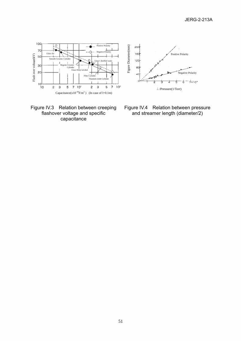
JERG-2-213A
51
Figure IV.3 Relation between creeping flashover voltage and specific
capacitance
Figure IV.4 Relation between pressure and streamer length (diameter/2)
Positive Polarity
⊥/Pressure(1/Torr)
Fig
ure
Dia
met
er(m
m)
Negative Polarity
Glass-Air
Smooth Ceramic Cylinder
Regular Ceramic Cylinder
Glass+Ethyl alcohol
Glass+ distilled water
Fibre Cylinder
Titanium oxide Cylinder
Positive Polarity
Negative Polarity
Fla
sh o
ver
volta
ge(k
V)
Capacitance(x10-10F/m2 ) (In case of l=0.1m)

JERG-2-213A
52
Table IV.1 Creeping discharge characteristics in vacuum and
in air (Electrode: Stainless-steel SUS)
IV2 Concept of preventing creeping surface discharge
In general, a creeping barrier is used to prevent a creeping discharge. A creeping
barrier, as shown in Figure IV.5, is composed of the insulation base with a surface on
which the originally creeping discharge develops, and a creeping barrier installed
approximately perpendicular to the base, which is called a “shade” or a “pleat.” The
insulation base, in practical application, corresponds to the “core” of a support
insulator or the “shell” of bushing. An electrode covering the insulation base
mounted on one side is called a back electrode. A support insulator has no back
electrode, although it corresponds to the core electrode of a bushing. In general, a
creeping discharge is likely to be longer in a structure with a back electrode. From
viewpoint of practical insulation, increasing the distance in creeping direction still
leads to a drop in the discharge voltage.
Also, it is effective to cover the whole creeping electrodes with coating. However,
enough consideration must be taken to prevent the enclosure of a layer of air or the
occurrence of cracks due to its thermal history.
Material Relative
permittivity εr
LengthofSpacer (mm)
Spacer Diameter
(mm)
Vacuum(10-6Pa)BreakdownElectricField(kV/mm)
Air(10-5Pa)BreakdownElectricField (kV/mm)
DC Inpulse
1.2/50μs AC
(peak) DC
Inpulse 1.2/50μs
AC (peak)
Teflon 2.1 2.0
4.0
7.0
7.0
16.0
10.9
15.1
10.3
12.8
8.5
2.75
2..45
2.80
2.50
2.80
2.45
Plastic
Glass 3.2 4.0 7.0 12.0 12.3 9.9 2.25 2.37 2.55
Quartz 3.8 5.0
6.5
9.5
9.5
8.6
8.2
8.6
8.3
7.8
7.1
2.9
2.7
2.9
2.7
2.7
2.7
Pyrex
Glass 4.6
2.0
4.0
6.35
6.35
16.5
11.5
15.5
11.1
14.0
9.9
3.75
2.36
3.75
2.45
3.75
2.63
Ceramic 5.8 2.0
4.0
7.0
7.0
16.6
12.6
16.2
12.5
14.25
10.25
2.50
2.50
2.50
2.45
2.75
2.63
Sapphire 12.0 3.1 12.55 9.0 8.4 7.3 1.81 1.87 1.94

JERG-2-213A
53
Figure IV.5 Example of barrier insulation structure
Creeping streamer
Grounding electrode
Creeping barrier HV electrode Creeping streamer
HV
Gap length
Insulation base
HV
(a) No Back electrode (Creeping streamer is reverse polarity to applied voltage)
(c) Back electrode grounded
(b) Back electrode is connected to HV (d) Back electrode is insulated
HV
HV
Back electrode

JERG-2-213A
54
References
[1] The Institute of Electrical Engineers of Japan, Discharge Handbook Publishing
Committee, “Discharge Handbook” (Ohmsha) (2003)