design of stripline-fed dual-polarization...
TRANSCRIPT

DESIGN OF STRIPLINE-FED DUAL-POLARIZATION
APERTURE-COUPLED STACKED MICROSTRIP PATCH PHASED
ARRAY ANTENNA FOR WIDEBAND APPLICATION
A Thesis
by
DAVID GEEHYUN KIM
Submitted to the Office of Graduate Studies of Texas A&M University
in partial fulfillment of the requirements for the degree of
MASTER OF SCIENCE
August 2010
Major Subject: Electrical Engineering

DESIGN OF STRIPLINE-FED DUAL-POLARIZATION
APERTURE-COUPLED STACKED MICROSTRIP PATCH PHASED
ARRAY ANTENNA FOR WIDEBAND APPLICATION
A Thesis
by
DAVID GEEHYUN KIM
Submitted to the Office of Graduate Studies of Texas A&M University
in partial fulfillment of the requirements for the degree of
MASTER OF SCIENCE
Approved by:
Chair of Committee, Kai Chang Committee Members, Robert D. Nevels Xing Cheng Boongyeol Ryoo Head of Department, Costas N. Georghiades
August 2010
Major Subject: Electrical Engineering

iii
ABSTRACT
Design of Stripline-Fed Dual-Polarization Aperture-Coupled Stacked
Microstrip Patch Phased Array Antenna for Wideband Application.
(August 2010)
David Geehyun Kim, B.S., Texas A&M University
Chair of Advisory Committee: Dr. Kai Chang
Recent days, antennas play an important role in wireless communication system. Microstrip
patch antennas are well known to have positive features for cost-effective, low profile and
broadband. This type of antenna can be used in wide range of applications such as in wireless
communications, radar systems, and satellites. Inhibiting characteristics of single patch antenna
with low gain and narrow band leads to the research area to have array configuration. Beam
steering antennas are the ideal solution for various systems such as traffic control and collision
avoidance radar systems.
The goal of this work is to design and implement a dual-linear polarization stacked microstrip
patch phased array antenna. Single stacked microstrip patch antenna fed by microstrip line was
designed to have approximately 3 GHz bandwidth in X-band with another ground plane to form
a stripline-fed. Stripline-fed design protects feed lines from any outside effects. The array
configuration was adapted to design in order to accomplish beam scan angle of ±30º by ±15º.
Binomial power distribution of 3x2 array structure was used in order to reduce grating lobes, and
changing length of feed lines was implemented for phase shifting. Bowtie cross shape aperture
and dual-offset microstrip feedline was used to feed radiating patches. For the feed network, T-

iv
split power divider was implemented and optimized to achieve low loss. The length of microstrip
line was adjusted to meet desired phase shift that in wideband application, the length of the line
had to be long enough to have similar wavelength response over broad frequency range. The
antenna array was designed using standard equations and simulated by electromagnetic analysis
software called Zealand’s IE3D which is method-of-moments based simulator. The resulting
measured impedance bandwidth and gain of both microstrip and stripline-fed single antenna are
43% and 5 to 10 dBi with low cross polarizations for all frequencies. The array antenna was
measured to have 29 to 60% impedance bandwidths depending on the different types of beam
scan angles. The gain of the array antenna is 8 to 13 dBi, and the beams are directed as required
with ±3º beam scan angle tolerance. The array antenna had a small offset as compared with
simulated results because of the fabrication process such as alignment, distorted feed lines while
etching, and etc, but the bandwidths and array patterns were acceptable.

v
ACKNOWLEDGEMENTS
First, I would like to wish a special thanks to a few people who helped guide me and achieve this
goal. I would like to thank my supervisor, Dr. Chang, for guiding me and helping me during the
course of this research work. I would also like to thank to Mr. Li, and other electromagnetic lab
members, for their guidance and technical assistance. I would like to thank Dr. Nevels, Dr.
Cheng, and Dr. Ryoo, for serving as members on my thesis committee.
All my thanks are due especially to my family members and friends for their support, prayers,
and inspiration.

vi
TABLE OF CONTENTS
Page
ABSTRACT .................................................................................................................................. iii
ACKNOWLEDGEMENTS ........................................................................................................... v
TABLE OF CONTENTS .............................................................................................................. vi
LIST OF TABLES ...................................................................................................................... viii
LIST OF FIGURES ....................................................................................................................... ix
CHAPTER
I INTRODUCTION .................................................................................................................. 1
I.1 Motivation of Research ................................................................................................... 1
I.2 Objectives of Research .................................................................................................... 2
II BACKGROUND .................................................................................................................. 3
II.1 Characteristics of Microstrip Antenna ........................................................................... 3
II.2 Excitation Techniques.................................................................................................... 4
II.2.1 Microstrip Line Feed ............................................................................................. 4
II.2.2 Coaxial Probe Feed ................................................................................................ 5
II.2.3 Aperture Coupling Feed ......................................................................................... 6
II.3 Array Antenna ............................................................................................................... 7
II.3.1 Typical Array Type ................................................................................................ 7
II.3.2 Phased Array .......................................................................................................... 8
II.3.3 Mutual Coupling .................................................................................................. 10
II.4 Power Divider .............................................................................................................. 11

vii
CHAPTER Page
III DESIGN OF SINGLE APERTURE COUPLED STACKED PATCH ANTENNA ......... 13
III.1 Important Design Parameters ..................................................................................... 13
III.1.1 Antenna Substrate ............................................................................................... 13
III.1.2 Resonant Frequency ........................................................................................... 15
III.1.3 Antenna Feed ...................................................................................................... 15
III.1.4 Polarization ......................................................................................................... 16
III.1.5 Patch Shape ........................................................................................................ 16
III.1.6 Stacked Patch...................................................................................................... 16
III.2 Simulation Results and Discussion ............................................................................ 17
III.2.1 Microstrip Line Feeding ..................................................................................... 17
III.2.2 Stripline Feeding ................................................................................................ 25
IV DESIGN OF PHASED ARRAY ANTENNA .................................................................. 32
IV.1 Design of Feed Network ............................................................................................ 32
IV.2 Design of Phased Array Antenna ............................................................................... 39
V FABRICATION AND TESTING ...................................................................................... 54
V.1 Single Stacked Patch Antenna (Microstrip Line-Fed, Stripline-Fed) .......................... 54
V.2 Stripline-Fed Phased Array Stacked Patch Antenna ................................................... 62
VI CONCLUSIONS AND FUTURE WORK ........................................................................ 79
REFERENCES ............................................................................................................................. 81
VITA ............................................................................................................................................ 84

viii
LIST OF TABLES
Page
Table 3.1 Thickness with real and imaginary impedances of microstrip feed line....................... 19
Table 3.2 Variables used for the microstrip feed line design (Initial value) ................................ 20
Table 3.3 Variables used for the microstrip feed line design (Final value) .................................. 24
Table 3.4 Thickness with real and imaginary impedances of stripline ......................................... 28
Table 3.5 Variables used for stripline feed design (Final value) .................................................. 30
Table 4.1 Variables used for corporate-fed array network ........................................................... 38
Table 4.2 Simulated results of the stripline-fed phased array antenna ......................................... 53
Table 4.3 Measured results of the stripline-fed phased array antenna.......................................... 65
Table 4.4 Measured gain and beam angle of the stripline-fed phased array antenna with 0º angle scan (3-element) ................................................................................................. 66
Table 4.5 Measured gain and beam angle of the stripline-fed phased array antenna with 0º angle scan (2-element) ................................................................................................. 66
Table 4.6 Measured gain and beam angle of the stripline-fed phased array antenna with 30º
angle scan ..................................................................................................................... 67
Table 4.7 Measured gain and beam angle of the stripline-fed phased array antenna with 15º angle scan ..................................................................................................................... 67

ix
LIST OF FIGURES
Page
Fig 2.1 Microstrip line feed ............................................................................................................ 4
Fig 2.2 Coaxial probe feed (L: length of the patch, W: width of the patch) ................................. 5
Fig 2.3 Aperture coupling feed ....................................................................................................... 6
Fig 2.4 Linear phased array configuration ...................................................................................... 8
Fig 2.5 Phase shift by changing frequency, length and ferrite material ....................................... 10
Fig 2.6 E- and H-plane arrangements of microstrip patch antennas ............................................. 11
Fig 2.7 T-split and Wilkinson power dividers .............................................................................. 12
Fig 3.1 Efficiency and bandwidth vs. substrate thickness at constant resonant frequency for rectangular microstrip patch ............................................................................................ 14
Fig 3.2 Geometry of aperture coupled stacked patch antenna with bowtie apertures and dual offset microstrip feed lines .............................................................................................. 17
Fig 3.3 Geometry of a dual offset microstrip feed line with bowtie aperture slot ........................ 19
Fig 3.4 VSWR comparisons for various size of patches, apertures and matching stubs of the antenna at feed1 and feed2 .............................................................................................. 22
Fig 3.5 S-parameter of the antenna with microstrip feed ............................................................. 23
Fig 3.6 S-parameter of the antenna with stripline feed (narrowband) .......................................... 26
Fig 3.7 Geometry of aperture coupled stacked patch antenna with bowtie apertures and dual offset stripline feed lines ................................................................................................. 27
Fig 3.8 S-parameter and VSWR of the antenna with stripline feed (broadband) ......................... 29

x
Page
Fig 4.1 Basic one-dimensional parallel feed networks ................................................................. 33
Fig 4.2 Mitered MBEND and 90º right angle MBEND, and Mitered T-Junction ........................ 33
Fig 4.3 S-parameter of two-way power divider with Mitered MBEND and 90º right angle MBEND ........................................................................................................................... 34
Fig 4.4 S-parameter comparison of 50Ω input to 140Ω output and 100Ω output of two-way power divider ................................................................................................................... 35
Fig 4.5 3-dB equal power divider and multi-section quarter-wave transformer........................... 36
Fig 4.6 Six-element weighted corporate-fed array network ......................................................... 36
Fig 4.7 S-parameter for 3 dB equal power divider and 100Ω to 50Ω transformer for the corporate-fed array feed. ................................................................................................. 37
Fig 4.8 Design and dimension of dual feed lines at 0º scan angle. ............................................... 41
Fig 4.9 Design and dimension of dual feed lines at 30º scan angle. ............................................. 42
Fig 4.10 Design and dimension of dual feed lines at 15º scan angle. ........................................... 43
Fig 4.11 Phase of each output lines for short and long feed lines at 0º angle scan
(No phase shift). ............................................................................................................. 46
Fig 4.12 Phase of each output lines for short and long feed lines at 30º angle scan
(-113.57º phase shift). .................................................................................................... 47
Fig 4.13 S-parameter of feed1 and feed2 of the array. ................................................................. 49
Fig 4.14 Geometry of a 3x2 phased array antenna. ...................................................................... 50
Fig 4.15 Top view of a 3x2 planar array antenna. ........................................................................ 51
Fig 4.16 Simulated S-parameter of the 0º beam scan array antenna. ........................................... 52

xi
Page
Fig 4.17 Simulated S-parameter of the 30º beam scan array antenna. ......................................... 52
Fig 4.18 Simulated S-parameter of the 15º beam scan array antenna. ......................................... 53
Fig 5.1 Actual picture of the single patch antenna. ...................................................................... 55
Fig 5.2 Isolation comparison of the antenna with microstrip line feed. ....................................... 56
Fig 5.3 VSWR comparison of the antenna with microstrip line feed. .......................................... 57
Fig 5.4 Measured radiation patterns for the antenna with microstrip line feed ............................ 58
Fig 5.5 Isolation comparison of the antenna with stripline feed ................................................... 59
Fig 5.6 VSWR comparison of the antenna with stripline feed ..................................................... 60
Fig 5.7 Measured radiation patterns for the antenna with stripline feed ...................................... 61
Fig 5.8 Actual picture of the array antenna before stacking. ........................................................ 62
Fig 5.9 Actual picture of the array antenna, layout and after assemble. ....................................... 63
Fig 5.10 Isolation comparison of the stripline-fed array antenna with 0º angle scan .................. 68
Fig 5.11 Isolation comparison of the stripline-fed array antenna with 30º angle scan ................ 68
Fig 5.12 Isolation comparison the stripline-fed array antenna with 15º angle scan .................... 69
Fig 5.13 VSWR comparison of the stripline-fed array antenna with 0º angle scan ................... 70
Fig 5.14 VSWR comparison of the stripline-fed array antenna with 30º angle scan .................. 71
Fig 5.15 VSWR comparison of the stripline-fed array antenna with 15º angle scan .................. 72
Fig 5.16 Measured radiation patterns for the stripline-fed array antenna with 0º angle scan (3-element) ..................................................................................................................... 73
xii
Page
Fig 5.17 Measured radiation patterns for the stripline-fed array antenna with 0º angle scan (2-element) ..................................................................................................................... 74
Fig 5.18 Measured radiation patterns for the stripline-fed array antenna with 30º angle scan (3-element) ..................................................................................................................... 75
Fig 5.18 Measured radiation patterns for the stripline-fed array antenna with 30º angle scan (2-element) ..................................................................................................................... 76
Fig 5.19 Measured radiation patterns for the stripline-fed array antenna with 15º angle scan (3-element) ..................................................................................................................... 77
Fig 5.19 Measured radiation patterns for the stripline-fed array antenna with 15º angle scan (2-element) ..................................................................................................................... 78

1
CHAPTER I 1
INTRODUCTION
I.1 MOTIVATION OF RESEARCH
Recently microstrip patch antennas are widely used often in antenna designs for their simplicity
and compatibility. Also they are an attractive type of antenna due to their low cost,
conformability, and ease of manufacture [1, 2]. Aperture coupled configuration also provides
many advantages such as isolating feed radiation by using ground plane. However, the primary
barrier to implementing these antennas in many applications is their limited bandwidth, low
efficiency and low gain [1, 2]. Over the years, a number of researches and tests have been carried
out to increase both bandwidth and radiation efficiency. One of the important proposals involved
in improving bandwidth is to increase heights by stacking radiating patch elements with aperture
coupling method. Also, arranging the radiating elements in one or two dimensionally will
increase gain of microstrip patch antennas.
Phased array antenna designs have received wide attention due to their significant role in radar
and satellite communication systems. The pattern of angular beams depends on the number of
elements, arrangement and relative signal amplitudes. There are several methods to implement
phased array antennas to have different signal strengths in order to control beams: the binomial
method, Dolph-Tschebysheff method, Taylor-Kaiser method, etc.
The journal model for this dissertation is IEEE Transactions on Microwave Theory and Techniques.

2
I.2 OBJECTIVES OF RESEARCH
The main goal of this project is to overcome these disadvantages and to develop antenna with the
following characteristics:
• X-band (8 to 12 GHz) frequency range
• ~3 GHz Bandwidth
• Dual-polarization
• Lightweight and Low loss
• Phased array with +/-30 deg by +/-15 deg scan
• Good polarization orthogonality at scan corners
Additional characteristics that will be pursued if time permits include:
• Compatible with sub-panel build up: planar, reasonable interface/balun structure
• Adding amplification and steering function built in
• Investigation of dielectric resonant antennas and fractal antennas as a possible
alternatives to the stacked patch

3
CHAPTER II
BACKGROUND
For the flat panel dual polarization phased array antenna, an aperture coupled stacked rectangular
microstrip patch radiator is proposed to reduce mutual coupling between two feed lines. Antenna
will consist of two microstrip patches on the top of ground with aperture and feed network
shaped in a single copper layer. The feed network will be designed to connect 50Ω transmission
line, which is the standard characteristic impedance for RF transmission lines. There are several
important factors need to be considered in designing wideband phased array microstrip patch
antenna: antenna substrate, size and shape of microstrip patch, shape of aperture on ground plane,
polarization of antenna and excitation techniques.
II.1 CHARACTERISTICS OF MICROSTRIP ANTENNA
Microstrip antennas are similar to parallel plate capacitors, in which one metal plate is extended
than the others to form a ground plane. Size of the patch is mostly proportional to the operating
frequency of the signal which is normally the resonance frequency of the patch. Due to this
characteristic, microstrip antennas have relatively narrow bandwidths, usually a few percents.
Several different shapes of patches, such as rectangular, circular, ring and etc. are employed in
various applications. The advantages of microstrip antennas are light weight, low profile, ease of
mass production, low fabrication cost, easy to integrate with other circuits, and various
polarization [1]. In contrast, the disadvantages are narrow bandwidths, low gain, and polarization
impurity [1].

4
II.2 EXCITATION TECHNIQUES
Microstrip antennas can be fed directly by microstrip line or coaxial probe, and it can be excited
using apertures on ground plane by coupling, which there is no physical contact with the
radiating element. The efficiency of antenna depends on power to the radiating element that
feeding technique is very important. Consequently, the feeding techniques have significant
impact on the power to the radiating element that determines the efficiency of the antenna.
II.2.1 MICROSTRIP LINE FEED
Microstrip line feeding methods are generally used for its easier fabrication, since the feed line
and radiating elements are in same surface of substrate. Impedance matching techniques are also
simpler in comparison to other methods. However, for broadband applications, microstrip line
feed antennas require thicker substrates, which increases surface waves and spurious feed
radiation. The large profile of microstrip antenna limits the bandwidths to typically 2~5% [2, 3].
This technique is shown in Fig 2.1.
Fig 2.1 Microstrip line feed

5
Input impedance of feed line is matched using insets of the feed line at the edge of the patch.
Moreover, quarter wave transformers or exponential tapers are introduced to match impedance
between the feed line and patch.
II.2.2 COAXIAL PROBE FEED
Coaxial probe feed techniques are arranged by soldering coaxial connector to the patch where
inner conductor is connected to patch and outer conductor to the ground plane. This technique is
shown in Fig 2.2. The main advantages of coaxial probe feeding are also easy to fabricate, match
input impedance, and its low spurious radiation [2]. However, it has the disadvantages of the
narrow bandwidth and the requirement of drilling hole to the thick substrate which is difficult to
model.
Fig 2.2 Coaxial probe feed (L: length of the patch, W: width of the patch)

6
Both microstrip line and coaxial probe feeding has inherent asymmetries which generates higher
modes that produce cross-polarization radiation [2]. To avoid these problems, aperture coupling
feed technique is introduced.
II.2.3 APERTURE COUPLING FEED
Aperture coupling consists of two substrates separated by a ground plane. As shown in Fig 2.3,
microstrip line feed is located below the ground plane, whose electromagnetic fields are coupled
to radiating patch through an aperture slot. The ground plane between substrates isolates feed
line from radiating patch that minimizes interference of spurious radiation and polarization
purity [2]. Several factors in this design of an excitation method, such as substrate parameter,
feed line width, slot size, shape, and position, decide the performance to improve bandwidth of
the antenna [4].
Fig 2.3 Aperture coupling feed

7
This approach increases the efficiency and bandwidth of antenna by separating the radiated
elements with the ground plane, giving a freedom to substrate parameter selection that minimizes
surface waves and spurious coupling with patch. However, the limitation comes from difficulty
to fabricate due to alignment of multiple layers that can result with errors and deteriorate in
performance.
II.3 ARRAY ANTENNA
Generally, the array structure is used to improve efficiency, directivity and gain of the antenna
system. Usually a single antenna has wide radiation patterns with larger beam angles with low
gain and poor efficiency. This is not acceptable for wireless communications, thus requires more
directive antennas. Array structure is basically a collection of radiating elements arranged in
specific manner to have wanted radiation patterns, gain and beam angle. The total field of the
array is determined by the vector addition of the fields radiated from each radiating element [2].
II.3.1 TYPICAL ARRAY TYPE
Two basic types of arrays are with uniform and non-uniform amplitude. The uniform amplitude
arrays are the simplest antennas that possess the largest directivity, narrow main lobe beam
width, and acceptable side lobe level [1, 2]. On the other hand, non-uniform amplitude arrays
can have more control over side lobe level. There are two most used techniques to apply non-
uniform, which are binomial and Dolph-Tschebyscheff. Each method has its own advantages and
disadvantages. Binomial arrays do not exhibit any minor lobes provided the spacing between the
elements is equal or less than one-half of a wavelength [2]. While binomial method arrays have

8
very narrow level of minor lobes, they exhibit larger beam widths. The major disadvantage of
binomial method is the wide variation between amplitudes of each element especially for larger
number of elements [2]. In contrast, Dolph-Tschebyscheff method has flexibility of choosing
ratio of main lobe and side lobe level. This method has uniform amplitude of side lobe levels that
it is often used desired to have largest possible spacing between elements.
II.3.2 PHASED ARRAY
Phased array is a special type of antenna that the radiating fields are scanned to have a desired
angle by introducing different excitation phase to each radiating elements. Configuration of
linear phased array antenna is shown in Fig 2.4. Phased array antennas are developed for radar
applications and spaced-based communication applications because of their capabilities of
scanning, weight and power [5]. Since the scanning must be continuous in phased array
technology, the system should be capable of continuously varying phase between elements [2].
Fig 2.4 Linear phased array configuration [6]

9
There are mainly four types of phase shifting techniques: by changing frequency, length,
permittivity and permeability. Phase shift techniques are shown in Fig 2.5.
Phase shifting by changing frequency is accomplished by series feeding of radiating elements
that elements are positioned in equal distance and changing frequency. This technique is taking
the electrical length into account that the physical lengths of the feeding lines are chosen at the
center frequency of the phased array antenna, and changing frequency will get the beam directed
to angles smaller or greater [6]. The technique is also called frequency scan phased array. It is
simple, but requires wide frequency operating range.
Phase shifting by changing its physical lengths can be applied to series-fed as well as corporate-
fed array antennas. For example, excitation phase can be controlled using PIN diodes that it
employs in forward and reverse bias which is often used as switching elements. Other ways of
switching are using hybrid-coupled phased shifter or digital switched phase shifter.
Phase shifting by changing permittivity is accomplished by using a gaseous discharge or plasma
which changes phase by changing the current through the device [6]. Phase shifting by changing
permeability uses electrically controlled ferromagnetic material. Ferrite phase shifter is
controlled by the magnetic field within the ferrite, which in turn is controlled by the amount of
current flowing through wires wrapped around phase shifter [2].

10
Fig 2.5 Phase shift by changing frequency (a), length (b) and ferrite material (c) [2]
II.3.3 MUTUAL COUPLING
When an array design has two or more elements near one another, they interfere with each other
on radiation characteristics such as the impedance and radiation pattern [2]. When two radiating
elements are positioned along the E-plane, very small spacing exhibits the smallest coupling
isolation, while the H-plane exhibits the small coupling for large spacing [2]. The E- and H-
plane arrangements of the elements are shown in Fig 2.6. By selecting the correct distance, these

11
fields can be decomposed to surface waves, and the spacing at which on plane coupling
overtakes the other one also depends on the electrical properties and the geometrical dimensions
of the microstrip antenna [2].
Fig 2.6 E- and H-plane arrangements of microstrip patch antennas
II.4 POWER DIVIDER
The phased array antenna requires power divider to feed each element. T-split power divider is a
simple three port network that can be used for power division or power combining which can be
implemented in virtually any type of transmission line medium [3]. It can be made to be matched
at all ports, equal-split or unequal power division ratios. Generally same as T-split power divider,
Wilkinson power divider relies on quarter wave transformer to match the split ports to common
port. As shown in Fig 2.7, Wilkinson introduced a resistor between two output ports to match,
which also improved the isolation. By definition, a 3 dB power divider is an ideally passive,
lossless, and reciprocal three port device that divides power equally in magnitude with equal

12
output phase [3]. For this design of array feed network, a 50Ω input line and two 100Ω output
lines are used to have 3 dB equal split power dividing.
Fig 2.7 T-split (left) and Wilkinson (right) power divider

13
CHAPTER III
DESIGN OF SINGLE APERTURE COUPLED
STACKED PATCH ANTENNA
Simulations were performed using Zealand’s IE3D [7], which is a method-of-moments based
electromagnetic simulator solver. Single antenna was also designed in Ansoft’s HFSS [8] to
compare with IE3D, and it was similar to each other. The copper etching on each substrate was
done in the etching facility at Texas A&M University using standard photolithography
techniques. All S-parameters were measured using an Agilent 8510C network analyzer. The
antenna pattern measurements were performed in the anechoic chamber of Electromagnetics and
Microwave Laboratory, Texas A&M University. The graphs were plotted using data exported
from IE3D and imported into PSI Plot. Microstrip line and stripline width for various
impedances were calculated using line width calculator provided by i-lab [9] found in web and
optimized by simulations.
III.1 IMPORTANT DESIGN PARAMETERS
III.1.1 ANTENNA SUBSTRATE
The radiation characteristics of a patch antenna is determined by the thickness and type of
substrate used. The impedance bandwidth and efficiency (η) of a patch antenna varies inversely
to one another. The parameters of dielectric constant (εr) and thickness (h) can be varied to
obtain different η, which will ultimately increase impedance bandwidth [1].

14
Fig 3.1 Efficiency and bandwidth vs. substrate thickness at constant resonant frequency
for rectangular microstrip patch [10]
As seen in Fig 3.1, decrease in the substrate dielectric constant and increase in the substrate
thickness increases the bandwidth of the antenna. However, thick substrates with high dielectric
substrates would result negatively on the radiation efficiency. Poor radiation efficiency will turn
out by the increase of surface wave propagation power and the poor impedance matching
problem due to increase in inductance of the probe-fed patch antenna [1]. Nevertheless, a thick
air dielectric substrate and aperture coupled feed antenna can avoid the above problems.

15
III.1.2 RESONANT FREQUENCY
The resonant frequency is a function of the length (L) of patch. Equation (1) can be used to
calculate the length at the dominant TM10 mode [1].
2 r r
cL
f ε=
⋅ ⋅ (1)
Here, fr is the resonant frequency, εr is the substrate dielectric constant and c is the speed of light.
Microstrip patch antenna has fringing fields at the edge that have a greater effect and should be
taken into consideration. Equation (2) accounts patch dimension for the fringing fields. ∆L is the
extended dimension for the fringing fields.
22
eff
r r
cL L
f ε= − ⋅∆
⋅ ⋅ (2)
III.1.3 ANTENNA FEED
As mentioned above, the aperture coupled feeding methods improve the bandwidth. Coupling
through the slot from the microstrip line feed occurs because the slot interrupts the longitudinal
current flow [1]. The aperture shape will vary the strength of coupling between feed network and
patch. Research has been done that the bowtie shape gives strong coupling through an aperture
[4]. Impedance matching plays an important role in patch antenna design and it can be
calculated with Equation (3) [11].
22290 cos
1r
Ar
L xZ
W L
ε πε
⋅∆ = ⋅ ⋅ ⋅ − (3)

16
The ∆x and W variables are the distance from edge of the patch to the feed point and patch width,
respectively.
III.1.4 POLARIZATION
Dual linear polarization is characterized by two orthogonal linear polarizations on the same
antenna that has an ability to transmit and receive the signal at the same time on single antenna.
III.1.5 PATCH SHAPE
Since the design requires dual polarization, both polarizations need to have their own bandwidth
at the same frequency. This requires that the orthogonal sides of the patch need to have the same
length. Square patch design will reduce the bandwidth, because the ratio of the width over the
length is greater than 1 and less than 2 [2].
III.1.6 STACKED PATCH
It is well known that multi layer structure is a useful method to improve the bandwidth. By
stacking a parasitic patch close to the fed patch widens bandwidth, two different sized patches
have two resonant frequencies near to each other and the wide bandwidth is obtained [12].
Bandwidth requirement can be met by selecting appropriate thickness of substrate and dimension
of patch.

17
III.2 SIMULATION RESULT AND DISCUSSION
III.2.1 MICROSTRIP LINE FEEDING
Fig 3.2 Geometry of aperture coupled stacked patch antenna with bowtie apertures and
dual offset microstrip feed lines
The antennas with the stacked patches’ distance less than 0.1λo have two resonant frequencies,
and as both variations of the input resistance and reactance are smaller, the wide bandwidth can
be obtained [12]. The model was optimized for a bandwidth of 3GHz in X-band and an isolation
of 20dB between the input ports. First, stacked patches were placed on the RT Duroid 3850
(permittivity of 2.90, loss tangent of 0.0001 and thickness of 2mil), and foam was used between

18
two patches. The foam (specially made for microwave application) used as the antenna substrate
has a permittivity of 1.06 and height of 3.2mm for the first fed patch and 1.6mm for second
stacked patch. The antenna used RT Duroid 5880 (permittivity of 2.20, loss tangent of 0.0001
and thickness of 20mil) for the both feed substrates that feed1 is at 0.508mm, and feed2 is at
1.016mm from the ground plane. Fig 3.2 shows the geometry for the initial antenna design.
For the feed network, dual-offset feed lines were used in order to reduce coupling and improve
the impedance match [13]. Moreover, this configuration does not suffer from the increased cross
polarization introduced by single feed line [13]. Other than many designs with two rectangular
feed lines with two separate slots, the dual-offset feed line allows the design to accomplish dual
polarization with two feeds sharing one aperture slot. In [14], an air bridge was used to provide a
crossover between the two orthogonal feed lines to reduce the number of substrates, but the
fabrication is too complicated. One of the feed was placed between patch and ground plane and
the other below the ground plane, so the feed lines will locate on opposite sides of the ground
plane in order to reduce coupling between two feedlines [15]. In this research’s design as shown
in Fig 3.3, a dual-offset feed line uses simple two-way power divider, which has two 100Ω lines
output from a single 50Ω line. The microstrip line widths were found using i-lab microstrip line
calculator and tuned with IE3D to have exact desired impedance. By using IE3D, feed line
thicknesses were matched to have at least above 25dB return loss. Exact impedance (Zo) can be
calculated using transmission line theory by making one side of the line to be short or open
circuits; the thickness of line was calculated and optimized at 9.5GHz in IE3D. Table 3.1 shows
real and imaginary parts of impedance calculated for each feed lines for microstrip feed line
antenna design.

19
Table 3.1 Thickness with real and imaginary impedances of microstrip feed line
Impedance Thickness (Value) Impedance Thickness (Value)
50Ω (feed1) 1.42mm (49.98 + j2.89) 50Ω (feed2) 3.75mm (50.05 – j3.98)
70.7Ω (feed1) 0.88mm (70.79 + j1.43) 70.7Ω (feed2) 2.14mm (70.73 – j3.94)
100Ω (feed1) 0.41mm (100.01 + j0.87) 100Ω (feed2) 1.08mm (100.02 – j3.84)
As mentioned above regarding square patch shape, the length and width of the patch are same.
The patch size (L) found to be 10.6mm and 12.5mm for stacked patch (L_p1) and fed patch
(L_p2), respectively. They were calculated by Equation (2) for resonant frequency of 10GHz,
and the permittivity of the foam (1.06) was used. Full dimensions of initial design are provided
in Table 3.2.
Fig 3.3 Geometry of a dual offset microstrip feed line with bowtie aperture slot

20
Table 3.2 Variable used for the microstrip feed line design (Initial value)
Variable Value Variable Value
Height of feed 1 substrate
(h_feed1) 0.508mm
Feed 1 matching stub length
(L_stub1) 2.5mm
Height of feed 2 substrate
(h_feed2) 0.508mm
Feed 2 matching stub length
(L_stub2) 2.5mm
Height of patch 1 substrate
(h_ant1) 1.6mm
Aperture 1 length
(L_slot1) 9.5mm
Height of patch 2 substrate
(h_ant2) 3.2mm
Aperture 1 end-width
(w_slot1) 1mm
Feed 1 width (100Ω)
(f1w_100) 0.41mm
Aperture 1 mid-width
(mid_slot1) 0.5mm
Feed 1 width (50Ω)
(f1w_50) 1.42mm
Aperture 2 length
(L-slot2) 9.5mm
Feed 2 width (100Ω)
(f2w_100) 1.08mm
Aperture 2 end-width
(w_slot2) 1mm
Feed 2 width (50Ω)
(f2w_50) 3.75mm
Aperture 2 mid-width
(mid_slot2) 0.5mm
Offset feed 1 separation
(d_off1) 2.5mm
Patch 2
(L_p1) 10.6mm
Offset feed 2 separation
(d_off2) 2.5mm
Patch 1
(L_p2) 12.5mm
Mitered T-Junction Feed1
(T1_mitered) 0.2015mm
Mitered T-Junction Feed2
(T2_mitered) 0.5065mm

21
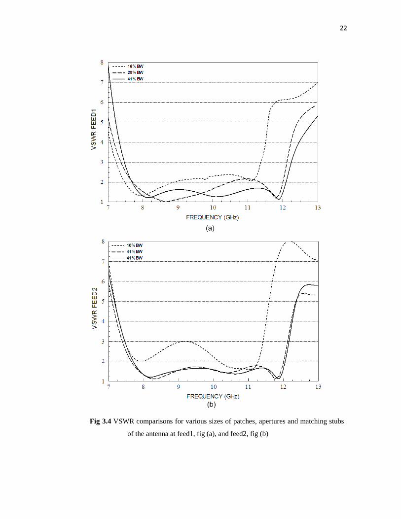
Initial design values resulted in bandwidth of 16% at center frequency of 8.13GHz for feed1 and
10% at center frequency of 10.73GHz for feed2. Isolation between both feeds was higher than
20dB which meets requirement.
After few runs of tuning patch sizes only, the length for resonance at 10GHz was found to be
10.2mm and 11.3mm for the patch2 and patch1, respectively. Patch size influenced high
frequency part of the patches’ two resonant frequencies. Bowtie aperture was used to couple the
feed line to the antenna, and tuning its length had effect on lower frequency of the band.
Aperture lengths dictate the amount of coupling [16], so increasing its length resulted in
increasing coupling between two feeds and increasing lower frequency, which decreases
bandwidth. By simulation, the best aperture dimension was found to have 1mm wide at the end
and 0.6mm at the middle with a length of 9.75mm and 10.0mm for feed1 and feed 2 respectively.
At this point, the best bandwidth results were 29% and 5% at feed1 and 41% at feed2. Feed1
resulted in dual frequency band that can be tuned to have much more wider bandwidth as feed2.
The next step was to tune matching stub lengths. The stub length takes significant role on
antenna performance. After few simulations, reducing the matching stub of feed1 from 2.5mm to
1.91mm and feed2 from 2.5mm to 2.28mm, the bandwidth was widened from to 41% at feed1
and 41% at feed2. Center frequencies were 9.9GHz for feed1 and 9.89GHz for feed2. In Fig 3.4,
simulated results of VSWR for each feeds are shown. The return loss of 10dB is equivalent to
VSWR of 2, so the portion of graph below 2 represents the bandwidth. For resonant frequency,
isolation between both feeds, which is red curve in Fig 3.5, was below 20dB. Fig 3.5 shows S-
parameter of finalized microstrip antenna design. Finalized design parameters are given in Table
3.3.
22
Fig 3.4 VSWR comparisons for various sizes of patches, apertures and matching stubs
of the antenna at feed1, fig (a), and feed2, fig (b)

23
Fig 3.5 S-parameter of the antenna with microstrip feed
Designing for aperture coupled stacked patch antenna with microstrip line feeding was finalized
and the next step was to change feeding method to stripline in order to shield the feed lines from
outside influence such as spurious feed radiation. The feed network and the radiator are
separated by a ground plane, thereby reducing interference in the element pattern from the feed
line radiation [16]. Moreover, the microstrip feed line distributes some of its fields into air region
which cannot support a pure TEM wave [3]. The stripline feeding, however, has all the fields
contained within a homogeneous dielectric region in which it can support a TEM wave and
higher order TM/TE modes [3].

24
Table 3.3 Variable used for the microstrip feed line design (Final value)
Variable Value Variable Value
Height of feed 1 substrate
(h_feed1) 0.508mm
Feed 1 matching stub length
(L_stub1) 1.91mm
Height of feed 2 substrate
(h_feed2) 0.508mm
Feed 2 matching stub length
(L_stub2) 2.28mm
Height of patch 1 substrate
(h_ant1) 1.6mm
Aperture 1 length
(L_slot1) 9.75mm
Height of patch 2 substrate
(h_ant2) 3.2mm
Aperture 1 end-width
(w_slot1) 1mm
Feed 1 width (100Ω)
(f1w_100) 0.41mm
Aperture 1 mid-width
(mid_slot1) 0.6mm
Feed 1 width (50Ω)
(f1w_50) 1.42mm
Aperture 2 length
(L-slot2) 10mm
Feed 2 width (100Ω)
(f2w_100) 1.08mm
Aperture 2 end-width
(w_slot2) 1mm
Feed 2 width (50Ω)
(f2w_50) 3.75mm
Aperture 2 mid-width
(mid_slot2) 0.6mm
Offset feed 1 separation
(d_off1) 2.5mm
Patch 2
(L_p1) 10.2mm
Offset feed 2 separation
(d_off2) 2.5mm
Patch 1
(L_p2) 11.3mm
Mitered T-Junction Feed1
(T1_mitered) 0.2015mm
Mitered T-Junction Feed2
(T2_mitered) 0.5065mm

25
III.2.2 STRIPLINE FEEDING
The main advantage of microstrip line feeding method is the simplicity of construction. However,
some microwave circuits of the feeding network are difficult to realize in a microstrip technique
such as 3dB coupled-line directional couplers being the key element of many feeding network,
cannot be straight forwardly designed in this technique [17]. Many researches have been done
regarding stripline-fed aperture coupled stacked patch antennas in order to reach dual
polarization, dual or wide bandwidth, and beam steering arrays. Stripline–fed antenna without
shorting pins or vias is proposed in [17], and it used additional slot on the ground plane, which
has exact same dimension with aperture coupling slot. In [18] a strip-line fed antenna is
introduced using vias around the aperture slots in order to have good return loss. Moreover,
stacked patch elements coupled through aperture with stripline using shorting pins are introduced
in [19]. Similar to [17], dual slot configuration was used to reach dual-band by tuning two
resonant frequencies [20]. In [16], dual aperture coupled circularly polarized patch antenna was
presented by placing two orthogonal rectangular slots beneath a square patch, and having equal
power split with 90º phase shift between the coupled ports. In [5], analyzing Stripline-fed
aperture antenna with different arbitrarily shaped apertures such as tapered rectangular, annular
ring, and circularly polarized slot by full-wave analysis method was presented to investigate
coupling between feed line and aperture. This analysis concluded exponentially tapered slot has
bandwidth up to 60º compared to 30º for the rectangular slot [5].
First, feeding network design was modified to be stripline feeding that now it has three dielectric
substrate layers below aperture slotted ground plane. Same substrate, RT Duroid 5880, was used,
and thickness and order was applied differently as microstrip design. The bottom and top layers

26
have ground planes with 60mil substrate, and feed1 and feed2 were inserted in the middle of 60
mil substrates with 10mil substrate. Stripline width was calculated using line width calculator
provided by i-lab found in web that 50Ω and 100Ω line width is 2.7mm and 0.7mm, respectively
for both feed1 and feed2. After few simulations with tuning design parameters, best aperture size
was found to be 1.6mm for end-width, 10mm length and 0.5mm for mid-width. The matching
stub lengths were modified to be 2.3mm for both feed lines. At this point, the best bandwidth
results were 26.0% at feed1 and 23.5% at feed2, which does not meet the design requirement.
Center frequencies were 8.86GHz for feed1 and 8.83GHz for feed2. Fig 3.6 shows the result of
the simulated S-parameters.
Fig 3.6 S-parameter of the antenna with stripline feed (narrowband)
In microstrip design, most of the fields from feed line are distributed towards single ground
plane. However, adding a ground plane for this stripline design weakens the field distribution, in

27
which they spread out to two different ground planes, resulting in a low coupling through
aperture. To overcome this problem, the model should be modified to keep most of the field
distribution towards upper ground plane.
Fig 3.7 Geometry of aperture coupled stacked patch antenna with bowtie apertures and
dual offset stripline feed lines
To redesign the stripline feed with stronger coupling through aperture, 4.8mm foam was added
between the feed substrate and bottom ground plane. As there was ground added to design, feed
line thickness had to be modified. Geometry of stripline feeding antenna design is shown in Fig
3.6 and Table 3.4 shows new feed line thickness.

28
Table 3.4 Thickness with real and imaginary impedances of stripline
Impedance Thickness (Value) Impedance Thickness (Value)
50Ω (feed1) 1.578mm (49.98 + j0.73) 50Ω (feed2) 3.3mm (50.01 – j2.68)
70.7Ω (feed1) 0.867mm (70.71 – j0.49) 70.7Ω (feed2) 1.926mm (70.71 – j1.91)
100Ω (feed1) 0.403mm (100.0 – j1.215) 100Ω (feed2) 1.013mm (99.99 – 1.93)
After the simulation, bandwidth results were 43% at feed1 and 44% at feed2. Center frequencies
were 9.89GHz for feed1 and 9.87GHz for feed2. For resonant frequency, isolation between both
feeds was below 20dB. S-parameter and VSWR plot is shown in Fig 3.8. Finalized design
parameters are given in Table 3.5.

29
Fig 3.8 S-parameter, fig (a) and VSWR, fig (b) of the antenna with stripline feed
(broadband)

30
Table 3.5 Variable used for the stripline feed design (Final value)
Variable Value Variable Value
Height of feed 1 substrate
(h_feed1) 0.508mm
Feed 1 matching stub length
(L_stub1) 1.98mm
Height of feed 2 substrate
(h_feed2) 0.508mm
Feed 2 matching stub length
(L_stub2) 2.07mm
Height of patch 1 substrate
(h_ant1) 1.6mm
Aperture 1 length
(L_slot1) 9.75mm
Height of patch 2 substrate
(h_ant2) 3.2mm
Aperture 1 end-width
(w_slot1) 1mm
Feed 1 width (100Ω)
(f1w_100) 0.403mm
Aperture 1 mid-width
(mid_slot1) 0.6mm
Feed 1 width (50Ω)
(f1w_50) 1.578mm
Aperture 2 length
(L-slot2) 10mm
Feed 2 width (100Ω)
(f2w_100) 1.013mm
Aperture 2 end-width
(w_slot2) 1mm
Feed 2 width (50Ω)
(f2w_50) 3.3mm
Aperture 2 mid-width
(mid_slot2) 0.6mm
Offset feed 1 separation
(d_off1) 2.5mm
Patch 2
(L_p1) 10.2mm
Offset feed 2 separation
(d_off2) 2.5mm
Patch 2
(L_p2) 11.3mm
Mitered T-Junction Feed1
(T1_mitered) 0.2015mm
Mitered T-Junction Feed2
(T2_mitered) 0.5065mm
Height of bottom foam
(h_foam) 4.8mm

31
CHAPTER IV
DESIGN OF PHASED ARRAY ANTENNA
Stacked patch antenna has attractive features for an array configuration because it can be used
without the need for increased element spacing and the associated grating lobe problem since
this design does not increase the surface area occupied by the elements and its radiation pattern
remains symmetrical over the operating band [1]. For an antenna array, microwave feed network
is often used to regulate the amplitude and phase of the radiating elements to control the beam
scanning properties. Thus selecting and optimizing the feed network is the critical requirement of
the phased array antenna design.
Many aperture coupled stacked patch phased array antenna have been studied with different kind
of feed lines in order to achieve their specific goals such as large phase shift, high isolation
between dual polarizing feeds, performance comparison, or steering function built in [21-23].
One of the researches presented steering function built in with the introduction of additional path
length of coaxial cable to tilt the beam up to 27º [6]. The problem associated with phased array
antenna can be beam distorting with scan angle, in which results in spread of the beam shape,
gain reduction, and high level of grating lobe [6].
An unequal Wilkinson power divider with the defected ground structure was designed to have
4:1 power distribution [24]. Unequal power divider is useful to excite un-uniform power
distribution on radiating elements in array antennas. In [25], an ultra-wideband (UWB) power
divider formed by installing a pair of stepped-impedance open-circuited stubs and parallel-
coupled lines to two symmetrical output ports was designed and analyzed to achieve 3.1 to

32
10.6GHz UWB range. In addition, a novel Wilkinson power divider with great performance
above X-band was presented in [26], and it uses opening up the two output branches by circular
shape and connecting the resistor to ends of the branches via λ/2 length of 50Ω transmission line.
Even though this paper, [26], is designed in narrowband, but the performances of power splitting
and loss has good characteristics. A wideband 12-way planar power divider/combiner with low
insertion loss less than 1dB was designed to have good characteristics over the band of 10 to
13GHz [27]. Many of the power divider design require resistors connected between output ports
in order to isolation, but for the stacked antenna application it is hard to add any materials which
can cause height difference between stacked elements.
IV.1 DESIGN OF FEED NETWORK
For the most common design, corporate feeding network is widely used as shown in Fig 4.1.
The fundamental configuration of a one-dimensional parallel feed consists of a branching
network of two-way power dividers in which if the distance from the input port to each element
is identical, the beam position is independent when the frequency and the feed is broadband [1].
By incorporating line extensions for each element, the beam direction can be controlled to
desired angles. The advantage of this design includes simpler design, flexible element spacing
and broad bandwidths. However, the disadvantage is that it requires longer transmission lines
between radiating elements and the input port, and the insertion loss of the feed network can be
large [1]. This design of the feed network consists of identical power dividers and quarter-wave
transformers, which are generally employed to match impedance at the junction of power divider.

33
Fig 4.1 Basic one-dimensional parallel feed networks
Equal power dividers will generate 3dB power from input port to two output ports. It requires T-
junction and microstrip bending (MBEND) modification to generate low insertion loss at the
input port. Mitered T-junction and microstrip bends were applied in order to have low reflection
and insertion losses. Experimental study of microstrip bends has been done to find out what kind
of bending techniques are useful in different antenna environments [28]. The mitered microstrip
bends and T-junction of 3dB power divider are shown in Fig 4.2.
Fig 4.2 (a) Mitered MBEND and (b) 90º right angle MBEND, and (c) Mitered T-
Junction

34
Definitions of the MBEND dimensions are following:
1.35
2
0.53 0.65 , for range 2.75, 25
22
W
Hr
D W
WX D e
H
DA X
ε−
= ⋅
= ⋅ + ≤ ≤
= ⋅ −
,
Mitered MBEND and 90º right angle MBEND were compared by designing two-way power
divider, 50Ω input to two 100Ω outputs, to see the differences in their losses, and the result in
Fig 4.3 shows that mitered MBEND two-way power divider has better return losses on specific
frequency range, but for the broadband side of view, 90º right angle MBEND had over 30dB
stable return losses. Therefore, the 90º right angle MBEND was used for whole design.
Fig 4.3 S-parameter of two-way power divider with (a) Mitered MBEND and (b) 90º
right angle MBEND
In the design, realizable high characteristic impedance feed line should be used to minimize the
feed line degradation [1], so 50Ω input to 140Ω output was also tested. 140Ω transmission line
thickness for feed1 was found to be 0.147mm, which is very thin line that might cause defect in

35
etching process. As shown in Fig 4.4, 100Ω output two-way power divider had lower reflection
loss than 140Ω output power divider. The advantage of 50Ω to 100Ω power divider is that it
does not require a quarter-wave transformer to match between input and output ports. Therefore,
50Ω to 100Ω power divider and 90º right angle microstrip line bend were chosen for the array
feed network.
Fig 4.4 S-parameter comparison of 50Ω input to (a) 140Ω output and (b) 100Ω
output of two-way power divider
The design of the array antenna will have 3x2 configurations with 1:2:1 power weighting
distribution to reduce complicated feed lines and grating lobe. Process of designing one 50Ω
input to six 50Ω input of dual-offset patch feed line is in following: 50Ω to 100Ω equal two way
power divider was used to have 3dB power division, and two output 100Ω lines were
transformed to 50Ω using 59.1Ω and 82.74Ω multi-section quarter-wave transformer. These two
power divider and multi-section quarter-wave transformer are used repeatedly to reach six
outputs (four 9 dB outputs and two 6 dB outputs). In this design, all of the multi-section quarter-
wave transformers and 3 dB equal power dividers are identical which it makes the design
simpler. Fig 4.5 shows a design of power divider and multi-section quarter-wave transformer and

36
Fig 4.6 shows full structure of corporate-fed array network design. Variables for the array feed
network are shown in Table 4.1.
Fig 4.5 (a) 3-dB equal power divider and (b) multi-section quarter-wave
transformer
Fig 4.6 Six-element weighted corporate-fed array network

37
S-parameters for power divider and 100Ω to 50Ω transformer line are shown in Fig 4.7. The
feed2 lines are thicker which means that they have more loss than feed1, but the 3dB power
divider worked very well in the range around 3.02~3.2dB for all X-band frequencies. A
completed full structure of feed line layout will be presented at Chapter IV section 2.
Fig 4.7 S-parameter for 3 dB equal power divider, fig (a) and (b), and 100Ω to
50Ω transformer, fig (c) and (d), for the corporate-fed array feed. Fig
(a) and (c) are feed1 and (b) and (d) are feed2

38
Table 4.1 Variables used for corporate-fed array network
Variable Value Variable Value
Feed 1 width (100Ω)
(f1w_100) 0.403mm
Feed 2 width (100Ω)
(f2w_100) 1.013mm
Feed 1 width (82.74Ω)
(f1w_82.74) 0.629mm
Feed 2 width (82.74Ω)
(f2w_82.74) 1.497mm
Feed 1 width (59.1Ω)
(f1w_59.1) 1.201 mm
Feed 2 width (59.1Ω)
(f2w_59.1) 2.57mm
Feed 1 width (50Ω)
(f1w_50) 1.578mm
Feed 2 width (50Ω)
(f2w_50) 3.30mm
Quarter-wavelength of
82.74Ω feed1 (λ1/4_1) 5.42mm
Quarter-wavelength of
82.74Ω feed2 (λ2/4_1) 5.82mm
Quarter-wave length feed1
59.1Ω feed1 (λ1/4_2) 5.44mm
Quarter-wave length feed1
59.1Ω feed2 (λ2/4_2) 5.73mm
Feed 1 mitered T-Junction
length of 50Ω to 100Ω
power divider (L1_t50)
0.8mm
Feed 2 mitered T-Junction
length of 50Ω to 100Ω power
divider (L2_t50)
2.2mm

39
IV.2 DESIGN OF PHASED ARRAY ANTENNA
Several different radiating element distances, (d), of 3x2 planar array were simulated to study
what distance would satisfy the requirements and also have best radiation patterns. The distances
were simulated from 0.5 to 1.0λ with 0.1λ increments. Binomial relative amplitude of 1:2:1
weighted power distribution was applied in order to reduce the grating lobes. Binomial arrays
with element spacing equal or less than 0.5λ have no side lobes [2], but unfortunately the gap
between elements were not enough for the dual polarization design. Also they have very low
minor lobes compare to other array types such as uniform and Dolph-Tschebyscheff amplitude
designs, but they exhibit larger beamwidths [2]. Binomial arrays do not have closed-form
express for a half power band width (HPBW) and a directivity (D) of any spacing between
elements [2], so it only can be calculated from the measured radiation patterns. Even though this
is a planar array, the design will be simulated and fabricated as linear array, since the testing
environment is suitable for positioning the antenna in accurate degree. Test simulation was done
separately for 0º, 30º and 15º scan angle. 15º scan angle is in y-direction which has 2 linear
elements layout, and 30º scan angle is in x-direction which has 3 linear elements. The phase shift
was calculated using equation (4). Equations (5) and (6) are for planar array design with two
different scan angles for both x- and y-directions.
cos okdβ θ= − - Linear array [2] (4)
sin cosx x o okdβ θ φ= − - Planar array [2] (5)
sin siny y o okdβ θ φ= − - Planar array [2] (6)

40
For 15º and 30º scan angles, phase shift (β) angles were -51.25º and -99º respectively. Because
the simulated radiation patterns shifted about 12º for 15º scan angle and 27º for 30º scan angle
only, -67.72º (20º scan angle) and -113.57º (35º scan angle) phase shifts were applied to achieve
the desired beam scan angles. From now on, even though 20º and 35º scan angle phase shift
were used, it will be stated as 15º and 30º.
As a result, 0.55 to 0.58λ gave the best outcome with higher than 20dB side lobe level (SLL) at
0º scan and around 10dB at 30º scan. Although 0.5 to 0.54λ had acceptable radiation patterns, the
space for feed lines was not sufficient to increase coupling between feed lines. Above 0.58λ
distance, the array resulted in less SLL value which was below 20dB at 0º scan and 8dB at 30º
scan. As the design requires precise alignment technique with different layers (8 layers total: 2
patches, 3 foams, 2 substrates and 1 ground plane), simulated SLL value should be preserved
high as possible to avoid error during fabrication. Therefore, the element distance of 0.55λ,
which is 17.37mm at 9.5GHz, was chosen and 6.27mm gap will be used for feed lines with
around 20dB SLL at 0º scan and 10dB SLL at 30º scan.
Before choosing 3x2 planar array design, a 4x2 design was considered since more elements can
achieve higher beam scan angle and narrower beam width. However, the 4x2 design requires
very complicated feed line structure for dual polarization, and longer lines had higher loss that
caused un-acceptable reflection and insertion loss. Moreover, the design was too bulky, with
dimension of 300mm by 300mm.

41
Fig 4.8 Design and dimension of dual feed lines at 0º scan angle

42
Fig 4.9 Design and dimension of dual feed lines at 30º scan angle

43
Fig 4.10 Design and dimension of dual feed lines at 15º scan angle

44
At first, 0º scan angle 3x2 planar array was designed, and 15º and 30º scan angles were adopted
to see whether the phase differences are well distributed throughout the desired frequencies. 0º,
30º, and 15º scan angle array feed line structures with dimensions are shown in Figs 4.8, 4.9 and
4.10, respectively.
Feed1 is design to feed radiating patches from left to right which are in same directions. Feed2,
however, has thicker line widths that didn’t have enough space to feed all the elements in the
same direction. As Fig 4.8 shows, half of feed2 lines were fed top to bottom and other half are in
opposite direction. This design required 180º phase shift at half of the lines to achieve the same
feeding direction, and it resulted in unstable insertion loss for each output lines.
Feed2 was re-designed to have all dual-offset feeding lines in same direction despite of space,
but coupling between lines created more unstable ripples at insertion loss than previous design.
Therefore, design with required 180º shift was used. Each feed lines have symmetric design that
unspecified dimensions can be found or predicted by the other half side of the feed lines.
After the feeding direction was chosen, feed line length was designed to have the shortest as
possible to avoid line loss and to have smaller size. The phase of each output lines within X-band
had offset by more than 10º. If the array is for narrowband, the feed lines can be short, because
the phase shift only needs to be set in narrow frequency bands. However as this array antenna is
for wideband application, desired phase would have to be similar in 3 to 4GHz frequency bands.

45
By simulating different lengths of feed lines where the phase shifting will be placed, it was
found that the line length had to be at least 2λo (60mm) at the output line, because longer lines
have more wavelength response through wide frequency range. With longer line lengths, phase
difference was only off by around 3º for entire X-band, which was acceptable. Figs 4.11 and
4.12 show the phase of each output lines (Feed1) for both short and long feed lines at 0º and 30º
scan angle, respectively. In Fig 4.11 (a), feed1 lines phase tuned to be same at 9GHz, but dotted
lines in plot have more wavelength responses than solid lines, except that phases were same at
only certain frequencies. The solid and dotted lines represent the divided each three feed lines
from first power divider of input port. Fig 4.12 (a) shows the result in bigger phase difference in
X-band when 30º angle scan phase shift is applied. In Fig 4.11 (b), longer feed lines have exactly
the same phase through the entire X-band, and beam scan angle of 30º phase shift also has a
similar wavelength response in X-band. These can be verified in Fig 4.12 (b). Output line lengths
where phase shifting applies are in the following: a short line was about 25mm (0.8λo) and a long
line about 60mm (2λo).

46
Fig 4.11 (a) Phase of each output lines for short and (b) long feed lines at 0º
angle scan (No phase shift)

47
Fig 4.12 (a) Phase of each output lines for short and (b) long feed lines at 30º
angle scan (-113.57º phase shift)

48
Finally, feed lines are optimized individually to have the least coupling between lines and to
avoid unexpected bouncing of insertion loss. S-parameter for the full structure of the corporate-
fed array feed network with 0º angle scan capability is shown in Fig 4.13, and both feed line
average insertion losses are around 6 to 7dB and 9 to 10dB, which is about 3dB difference. Also
the result shows that feed1 has more stable insertion loss because feed2 network has a slightly
higher insertion loss caused by line loss and coupling through the structure due to their thicker
lines. Since the gap between elements is 6.3mm, little coupling effect between lines cannot be
avoided. When the built-in phased shifter by changing length is placed in order to tilt 0º and 30º,
the insertion loss was increased due to line length increase and coupling. These increased
insertion loss are inevitable, so the lines were again optimized to reduce any negative effects on
the antenna performance.
Next step is to locate radiating elements and apertures to complete the array design. Figs 4.14
and 4.15 show geometry of a full structure and the top view of array design, respectively. The
size of the antenna is 200 x 160 x 1.1mm.

49
Fig 4.13 (a) S-parameter of feed1 and (b) feed2 of the array

50
Fig 4.14 Geometry of a 3x2 phased array antenna

51
Fig 4.15 Top view of a 3x2 phased array antenna
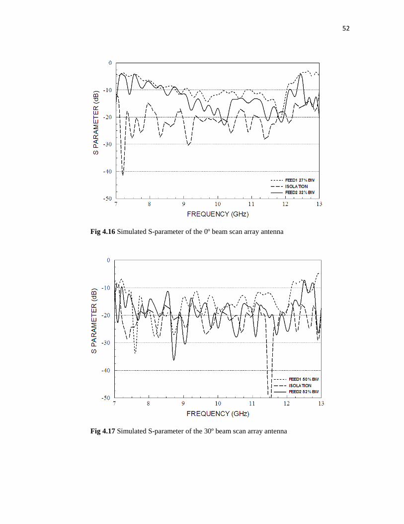
Simulated S-parameter for each 0º, 30º and 15º angle scan array antenna are shown in Figs 4.16,
4.17, and 4.18 respectively. The detailed reading of the simulated result is listed in Table 4.2. As
the array structure and phase shift increased feed line lengths, the reflection loss have changed
that the bandwidth became narrower or wider than the single stacked patch antenna. Isolation
between feed lines increased by 5 to 10dB than single stacked patch antenna since the feed lines
cannot avoid crossovers. Simulated radiation pattern will be presented and compared with
measured data in Chapter V.
52
Fig 4.16 Simulated S-parameter of the 0º beam scan array antenna
Fig 4.17 Simulated S-parameter of the 30º beam scan array antenna

53
Fig 4.18 Simulated S-parameter of the 15º beam scan array antenna
Table 4.2 Simulated results of the stripline-fed phased array antenna
Beam Scan
Angle Feed # Bandwidth
Center
Frequency
(GHz)
Operating
Frequency
(GHz)
0º Feed1 27% 10.6 9.2 ~ 12.0
Feed2 32% 10.6 8.9 ~ 12.3
30º Feed1 50% 9.7 7.3 ~ 12.1
Feed2 52% 9.85 7.3 ~ 12.4
15º Feed1 45% 10.35 8.0 ~ 12.7
Feed2 42% 10.15 8.0 ~ 12.3

54
CHAPTER V
FABRICATION AND TESTING
V.1 SINGLE STACKED PATCH ANTENNA (MICROSTRIP LINE-F ED, STRIPLINE-
FED)
The fabrication of antennas was done with the substrates and foams. For the best result, patches
should be placed in the air or etched on the foam but could not be etched on foams. They were
etched on RT Duroid 3850 which has a dielectric constant of 2.9 and a thickness of 2mil
(0.0508mm) which is the thinnest substrate available.
High resolution negative film was used to etch the design to substrates. An actual picture of
single antenna is shown in Fig 5.1. The circular dots on the edge of the substrates are used to
align the substrates and a careful alignment process was used to eliminate any human errors.
Because errors can occur in producing negative films, comparing the films with circled dots was
very important process in fabrication.
Patches, apertures in the ground plane and the feed lines were etched to their specific substrates
through photolithography, which is the process to remove selected parts of coppers on the
substrate using a thin film. UV light was used to transfer design on the film to substrate. A series
of chemical treatments etched away the coppers that were unprotected by the film.
After all the copper layers were etched away, substrates and foams were cut to have same
dimension as the ground plane. A 3.5mm SMA connector was soldered to the upper ground

55
plane and to the input of feed line. Below feed line substrates, a 4.8mm foam was placed and a
26oz zinc plated steel was placed for the bottom ground plane. Again, the other end of the SMA
connector was soldered to the bottom ground plane. On the top of the upper ground plane, a
3.2mm thick foam was layed down and the first patch Duroid substrate followed. Next, a 1.6mm
thick foam was layed down and the second patch Duroid substrate was positioned. The foam had
adhesive back on one side and the other side was attached by 3M spray adhesive [29]. The
adhesive foam was assumed to have little effect on performance of the antenna.
Fig 5.1 Actual picture of the single patch antenna
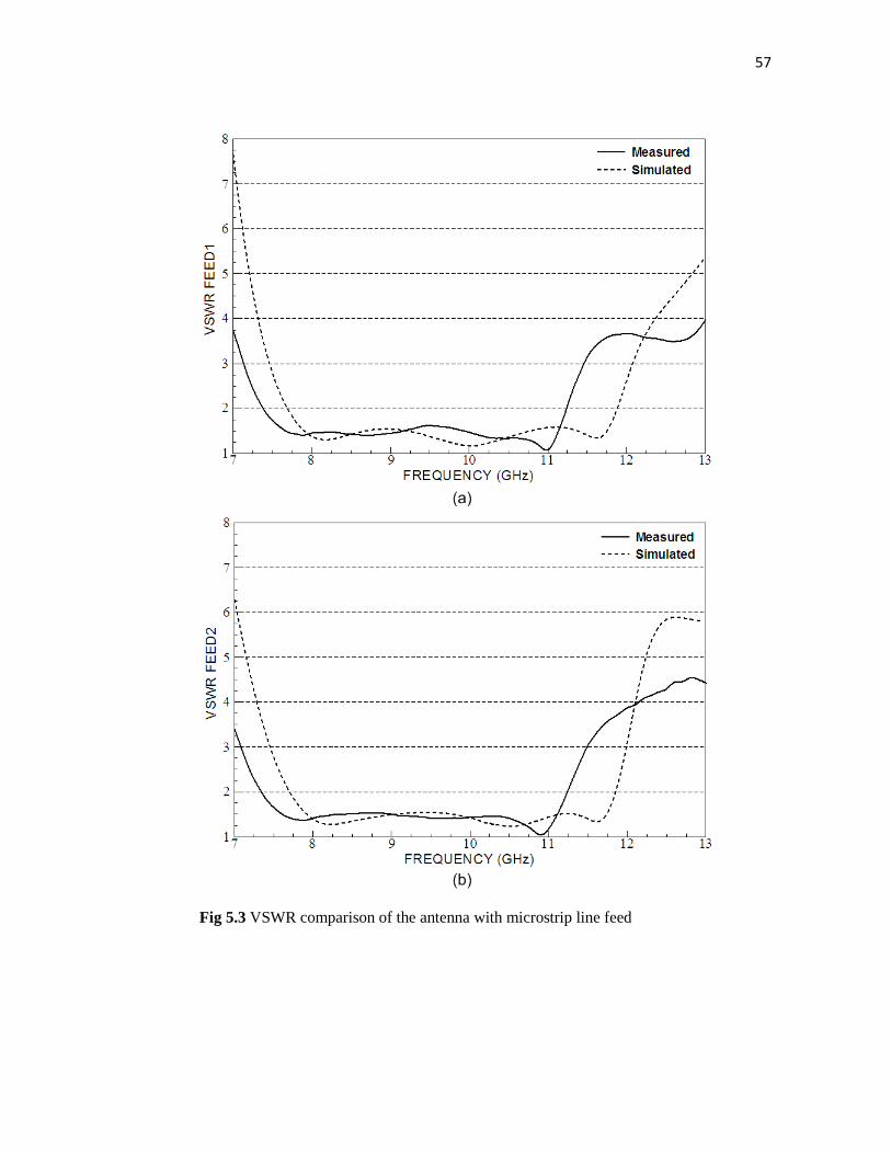
The isolation and VSWR of each feeds for simulated and measured value of the antenna with
microstrip line feed are shown in Figs 5.2 and 5.3. The frequency range was shifted about
0.5GHz less than the simulated result, and the bandwidth was 42% from 7.3 to 11.2GHz with
better than 25dB of isolation between two feeds. The radiation patterns of the microstrip line-fed
aperture coupled stacked antenna at 9, 10 and 11GHz are shown in Fig 5.4 that “co-pol” is for E-
plane measurements and “cross-pol” is for H-plane. Performance of linearly polarized antenna is

56
described as its principal E- and H-plane patterns in which the E-plane/H-plane contains the
electric/magnetic-field vector and direction of maximum radiation [2]. The antenna gain of the
dual feed antenna constructed was between 6 to 10 dBi for all frequencies measured. The
antenna gain was higher than it was expected for a single antenna. The cross-polarization levels
were about 15 dB or greater than the main beam, and the antenna has good isolation. The HPBW
can be calculated from -3 dB value of its maximum of radiation pattern. The measured HPBW
values were 85º ~ 99º for both feedlines which exhibit very wide beam and no minor lobes.
Fig 5.2 Isolation comparison of the antenna with microstrip line feed
57
Fig 5.3 VSWR comparison of the antenna with microstrip line feed

58
Fig 5.4 Measured radiation patterns for the antenna with microstrip line feed

59
The isolation and VSWR of each feeds for simulated and measured value of the antenna
with stripline feed are shown in Figs 5.5 and 5.6. As the stripline feed method has very
similar structure as microstrip feed line except bottom foam and ground plane, the
antenna bandwidth was almost identical as the microstrip one. The frequency range was
also shifted about 0.5 GHz less than the simulated result, and the bandwidth was 43%
from 7.2 to 11.2 GHz with below 25 dB of isolation between two feeds. The radiation
patterns of the stripline-fed aperture coupled stacked antenna at 8.5, 9.5 and 10.5 GHz are
shown in Fig 5.7, and the patterns were very similar as expected to the microstrip line-fed
antenna. The antenna gain of the dual feed antennas constructed was between 6 to 9 dBi
for all frequencies measured. The cross-polarization levels were about 10 dB or greater
than the main beam that the antenna has acceptable isolation. The measured HPBW
values were 79º ~ 95º for both feedlines.
Fig 5.5 Isolation comparison of the antenna with stripline feed

60
Fig 5.6 VSWR comparison of the antenna with stripline feed

61
Fig 5.7 Measured radiation patterns for the antenna with stripline feed

62
V.2 STRIPLINE-FED PHASED ARRAY STACKED PATCH ANTENN A
Fig 5.8 Actual picture of the array antenna before stacking

63
Fig 5.9 Actual picture of the array antenna, layout and after assemble
Actual pictures of array antenna are shown in Figs 5.8 and 5.9. Measured isolations of the
phased array antennas are around 20dB, and they are very similar to simulated value or
lower as in Figs 5.10, 5.11, and 5.12. As mentioned in Chapter IV, the reaction of feed
line crossovers generated coupling, so the isolation became higher with the array antenna.

64
The VSWR of each feeds for simulated and measured of array antenna are shown in Figs
5.13, 5.14, and 5.15. The detailed reading of the measured result is listed in Table 4.3.
From Fig 5.15 VSWR of feed2, a little pop out at 10.3GHz was ignored when calculating
bandwidth. Overall, the measured bandwidths of the array antennas are wider than the
simulated by 5% which meets requirements.
Radiation patterns for several frequencies of each array antenna are shown in Figs 5.16 to
5.21, and details of reading are presented in Tables 4.3 to 4.7. The patterns had around 8
to 13dBi gain between several different frequencies and beams were directed toward ±3º
range of desired beam angle. The simulated patterns had beam directed as designed, but
the actual antenna resulted in offset on beam angles due to problems with alignment,
distorted feed lines in etching process, or air bubbles while stacking the antenna elements.
Main beam shape was divided into two or three beams in some frequencies, and it seems
that the major problem was alignment of elements which resulted in different beam
angles on each radiating elements. Moreover, the phase shift by changing line lengths
caused ripples on power dividers in that power distribution was not exactly 1:2:1 through
operating frequencies. Even though the beam divided into two or three beams, the beam
angle has been shifted as desired. Feed2 at 9.6GHz of 15º angle scan array antenna, for
example, two max gains were 10.45dBi at 10º and 9.6dBi at 21º, and the mean angle was
at 15.5º with 9.6dBi gain. This can be interpreted by the problem during alignment
process in fabrication, not from the phase shift. Another problem with the pattern is
shown in Fig 5.19, where the pattern seems to be canceled out by relative elements. The
reason of low gain pattern is not verified, and it needs to be investigated. Overall, the
beams are shifted to required angles with good gain. The HPBW values of the 3-element

65
linear array parts were 17º ~ 39º for three different designs, and 30º ~ 48º for 2-element
linear array parts. Since the measured pattern beam shapes were not consistent through
operating frequencies, the HPBW difference was larger than the single antenna. However,
it can be easily seen that the measured HPBW is narrower than simulated pattern. If
there was alignment machine available, the array antenna could have been stacked
precisely, and the measured results will be much more accurate.
Table 4.3 Measured results of the stripline-fed phased array antenna
Beam Scan
Angle Feed # Bandwidth
Center
Frequency
(GHz)
Operating
Frequency
(GHz)
0º Feed1 31% 10.1 8.5 ~ 11.7
Feed2 29% 10.5 9.0 ~ 12.0
30º Feed1 60% 10.0 7.0 ~ 13.0
Feed2 50% 9.36 7.0 ~ 11.7
15º Feed1 49% 9.46 7.1 ~ 11.8
Feed2 49% 9.28 7.0 ~ 11.6
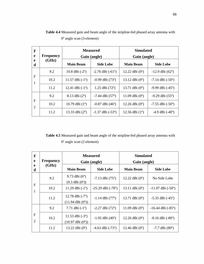
66
Table 4.4 Measured gain and beam angle of the stripline-fed phased array antenna with
0º angle scan (3-element)
Table 4.5 Measured gain and beam angle of the stripline-fed phased array antenna with
0º angle scan (2-element)
Feed
Frequency (GHz)
Measured
Gain (angle)
Simulated
Gain (angle)
Main Beam Side Lobe Main Beam Side Lobe
F
1
9.2 10.8 dBi (-2º) -2.76 dBi (-61º) 12.22 dBi (0º) -12.9 dBi (62º)
10.2 11.57 dBi (-1º) -0.99 dBi (73º) 13.12 dBi (0º) -7.14 dBi (-50º)
11.2 12.41 dBi (-1º) 1.25 dBi (72º) 13.71 dBi (0º) -9.99 dBi (-45º)
F
2
9.2 8.13 dBi (2º) -7.44 dBi (57º) 11.09 dBi (0º) -9.29 dBi (55º)
10.2 10.79 dBi (1º) -0.87 dBi (46º) 12.26 dBi (0º) -7.55 dBi (-50º)
11.2 13.33 dBi (2º) -1.37 dBi (-53º) 12.56 dBi (1º) -4.9 dBi (-40º)
Feed
Frequency (GHz)
Measured
Gain (angle)
Simulated
Gain (angle)
Main Beam Side Lobe Main Beam Side Lobe
F
1
9.2 9.73 dBi (6º)
(9.3 dBi (0º)) -7.13 dBi (75º) 12.22 dBi (0º) No Side Lobe
10.2 11.29 dBi (-1º) -25.29 dBi (-78º) 13.11 dBi (0º) -11.97 dBi (-50º)
11.2 12.78 dBi (-7º)
(11.94 dBi (0º)) -1.14 dBi (77º) 13.71 dBi (0º) -5.35 dBi (-45º)
F
2
9.2 7.71 dBi (-1º) -2.27 dBi (72º) 11.09 dBi (0º) -16.44 dBi (-85º)
10.2 11.53 dBi (-3º)
(10.97 dBi (0º)) -1.95 dBi (40º) 12.26 dBi (0º) -8.16 dBi (-80º)
11.2 13.22 dBi (0º) -4.63 dBi (-73º) 12.46 dBi (0º) -7.7 dBi (80º)

67
Table 4.6 Measured gain and beam angle of the stripline-fed phased array antenna with
30º angle scan (3-element)
Feed
Frequency
(GHz)
Measured
Gain (angle)
Simulated
Gain (angle)
Main Beam Side Lobe Main Beam Side Lobe
F
1
9.1 9.61 dBi (-32º) 1.57 dBi (17º) 11.13 dBi (-30º) -3.26 dBi (15º)
10.0 10.24 dBi (-27º) 2.3 dBi (19º) 11.48 dBi (-28º) 1.59 dBi (50º)
11.1 10.43 dBi (-24º)
(8.7 dBi (-30º)) 4.55 dBi (32º) 11.5 dBi (-30º) 5.1 dBi (40º)
F
2
9.1 8.16 dBi (-32º) 3.5 dBi (21º) 10.49 dBi (-30º) 3.18 dBi (20º)
10.0 12.55 dBi (-33º) 4.25 dBi (15º) 10.62 dBi (-30º) 2.0 dBi (55º)
11.1 11.12 dBi (-29º) 3.96 dBi (53º) 11.45 dBi (-28º) 4.02 dBi (55º)
Table 4.7 Measured gain and beam angle of the stripline-fed phased array antenna with
15º angle scan (2-element)
Feed
Frequency
(GHz)
Measured
Gain (angle)
Simulated
Gain (angle)
Main Beam Side Lobe Main Beam Side Lobe
F
1
8.8 13.07 dBi (15º) 2.8 dBi (-49º) 11.78 dBi (17º) 2.46 dBi (-55º)
9.6 10.44 dBi (14º) -4.46 dBi (-58º) 12.78 dBi (13º) -0.8 dBi (-60º)
10.6 9.3 dBi (13º) -0.55 dBi (-51º) 13.23 dBi (13º) 0.5 dBi (-60º)
F
2
8.8 12.57 dBi (16º) 0.34 dBi (-45º) 10.15 dBi (13º) -4.55 dBi (55º)
9.6 10.45 dBi (10º)
(9.95 dBi (15º)) 3 dBi (-50º) 11.55 dBi (15º) -2.72 dBi (-60º)
10.6 11.1 dBi (5º)
(9.9 dBi (15º)) 2.37 dBi (-50º) 12.18 dBi (13º) -3.23 dBi (-75º)

68
Fig 5.10 Isolation comparison of the stripline-fed array antenna with 0º angle scan
Fig 5.11 Isolation comparison of the stripline-fed array antenna with 30º angle scan

69
Fig 5.12 Isolation comparison of the stripline-fed array antenna with 15º angle scan

70
Fig 5.13 VSWR comparison of the stripline-fed array antenna with 0º angle scan
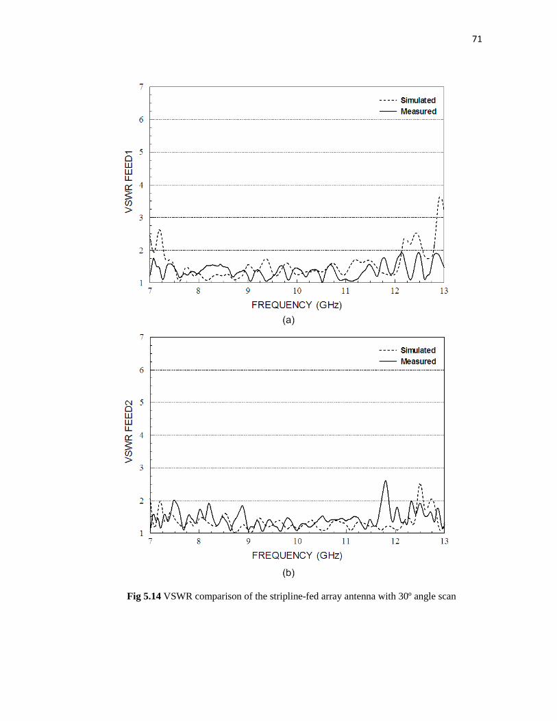
71
Fig 5.14 VSWR comparison of the stripline-fed array antenna with 30º angle scan

72
Fig 5.15 VSWR comparison of the stripline-fed array antenna with 15º angle scan

73
Fig 5.16 Measured radiation patterns of the stripline-fed array antenna with 0º angle
scan (3-element)

74
Fig 5.17 Measured radiation patterns for the stripline-fed array antenna with 0º angle
scan (2-element)

75
Fig 5.18 Measured radiation patterns for the stripline-fed array antenna with 30º angle
scan (3-element)

76
Fig 5.19 Measured radiation patterns for the stripline-fed array antenna with 30º angle
scan (2-element)

77
Fig 5.20 Measured radiation patterns for the stripline-fed array antenna with 15º angle
scan (3-element)

78
Fig 5.21 Measured radiation patterns for the stripline-fed array antenna with 15º angle
scan (2-element)

79
CHAPTER VI
CONCLUSIONS AND FUTURE WORK
As in the simulation results and measured sections, the bandwidth of 3GHz in X-band has been
achieved with 20dB isolation. The requirements have been met by using an aperture coupled
stacked patch antenna. The shape of aperture was designed to accomplish dual polarization with
increased bandwidth. The stacked patch with other modifications made the antenna to have 43%
bandwidth because two radiating patches have two near resonant frequencies. The single stacked
patch antenna had 5 to 10 dBi gain over the operating frequencies with low cross-polarization.
Phase shifting by changing feed lengths were adapted to reach ±30º by ±15º beam scan angle.
The bandwidth of the array antenna was even wider up to 60%. The array antenna with 30º angle
scan has been measured from 7.0 to 13 GHz, and it covered all of the X-band frequency range.
The actual bandwidth of this antenna was about 90% from 5.5 to 14.5 GHz. This was greater
than expected with simulation results. The array antenna had 8 to 13 dBi gain, and the beam scan
angles are within ±3º tolerance. Some of the main beams were divided into two or three beams
because of the process of fabrication, but the beams shifted as desired.
The aperture coupled stacked patch phased array antenna can be used in various applications
such as radar and satellite communication systems. The dual polarization will allow transmit and
receive signals at once with one single antenna in which it can reduce the cost of production. In
addition, stripline-fed design can be effective since the feed lines will be protected from outside
influence such as spurious feed radiation and other environment effects.

80
Further investigations can be made to this wideband dual polarization antenna by using dielectric
resonant antennas (DRA) and fractal antennas could be investigated as possible alternatives to
the stacked patches. Also amplification and steering functions could be built in with this antenna
which can reduce the size and number of antennas. These topics show great potentials for
wideband antenna design using simpler structures. Moreover, this dual polarization array
antenna can be modified to produce a circular polarized single-beam by combining the two feeds
together with a 90º phase shift on one of the feeds.

81
REFERENCES
[1] R. Garg, P. Bhartia, I. Bahl, and A. Ittipiboon, Microstrip Antenna Design Handbook, 2nd ed. Norwood, MA: Artech House, 2001.
[2] C. A. Balanis, Antenna Theory, 3rd ed. Hoboken, NJ: John Wiley & Sons, 2005.
[3] D. M. Pozar, Microwave Engineering, 3rd ed. Hoboken, NJ: John Wiley & Sons, 2005.
[4] V. Rathi, V., G. Kumar, and K. P. Ray, “Improved coupling for aperture coupled microstrip antennas,” IEEE Trans. Antennas Propagat., vol. 44, no. 8, pp. 1196-1198, Aug. 1996.
[5] C. Chen, W.E. Mckinzie, and N.G. Alexopoulos, “Stripline-fed arbitrarily shaped printed-
aperture antennas,” IEEE Trans. Antennas Propagat., vol. 45, no. 7, pp. 1186-1198, Jul. 1997.
[6] J. Ehmouda, Z. Briquch, and A. Amer, “Steered microstrip phased array antennas,” World
Academy of Science, Engineering and Technology, no. 49, pp. 319-323, Jan. 2009. [7] IE3D v14.10. Computer software. Zealand, LLC, 2008
[8] HFSS v12.0. Computer software. Ansoft, LLC, 2008
[9] I-Laboratory. (Oct. 1997). Line calculator. [Online]. Available: http://www1.sphere.ne.jp/i-
lab/ilab.
[10] D. M. Pozar, “Microstrip antennas,” in Proc. IEEE, vol. 80, no. 1, Jan. 1992, pp. 79-91.
[11] W. L. Stutzman and G. A. Thiele, Antenna Theory and Design, 2nd ed. Hoboken NJ: John Wiley & Sons, 1997.
[12] E. Nishiyama, M. Aikawa, and S. Egashira, “Three-element stacked microstrip antenna with
wide-band and high-gain performances,” in IEEE Antennas and Propagat. Society Int. Symp., vol. 2, U.S.A., Jun. 2003, pp. 900-903.
[13] S. D. Targonski, R. B. Waterhouse, and D. M. Pozar, “Design of wide-band aperture-
stacked patch microstrip antenna,” IEEE Trans. Antennas Propagat., vol. 46, no. 9, pp. 1245-1251, Sep. 1998.
[14] C. H. Tsao, Y. M. Hwang, F. Kilburg, and F. Dietrich, “Aperture-coupled patch antennas
with wide-bandwidth and dual-polarization capabilities,” in IEEE Antennas and Propagat. Society Int. Symp. Dig., Vol. 3, U.S.A., June 1988, pp. 936-939.

82
[15] M. Yamazaki, E.T. Rahardjo, and M. Haneishi, “Construction of a slot-coupled planar antenna for dual polarization,” IET Electronics Letters, vol. 30, no. 22, pp. 1814-1815, Oct. 1994.
[16] A. Adrian, D.H. Schaubert, “Dual aperture-coupled microstrip antenna for dual or circular polarisation,” IEEE Electronics Letters, vol. 23, no. 23, pp. 1226-1228, Nov. 1987.
[17] K. Wincza, S. Gruszczynski, and K. Sachse, “Aperture coupled to stripline antenna element
for integrated antenna arrays,” IET Electronics Letters, vol. 42, no. 3, pp. 130-131, Feb. 2006.
[18] A. Bhattacharyya, O. Fordham, and Y. Liu, “Analysis of stripline-fed slot-coupled patch
antennas with vias for parallel-plate mode suppression,” IEEE Trans. Antennas Propagat., vol. 46, no. 4, pp. 538-545, Apr. 1988.
[19] P. Brachat, and J.M. Baracco, “Dual-polarization slot-coupled printed antennas fed by
stripline,” IEEE Trans. Antennas Propagat., vol. 43, no. 7, pp. 738-742, Jul. 1995. [20] M. Wong, A.R. Sebak, and T.A. Denidni, “Analysis of a dual-band slot omnidirectional
stripline antenna,” IEEE Antennas and Wireless Propagat. Letters, vol. 6, pp. 199-202, Apr. 2007.
[21] F.F. Dubrovka, and S.Y. Martynyuk, “Wideband dual polarized planar antenna arrays,”
International Conf. on Antenna Theory and Tech., vol. 1, pp 91-96, Sep. 2003. [22] R. B. Waterhouse, “Design and performance of large phased arrays of aperture stacked
patches,” IEEE Trans. Antennas Propagat., vol. 49, no. 2, pp. 292-297, Feb. 2001. [23] J. Huang, G. Shadowy, C. Derksen, L. Del Castillo, P. Smith, et al, “Aperture-coupled thin-
membrane microstrip array antenna for beam scanning application,” IEEE Antennas and Propagat. Symp., vol. 1A, pp. 303-333, Jul. 2005.
[24] J. Lim, S. Lee, C. Kim, J. Park, D. Ahn, et al, “A 4:1 unequal Wilkinson power divider,”
IEEE Microwave Wireless Components Letters, vol. 11, no. 3, pp. 124-126, Mar. 2001. [25] S.W. Wong, and L. Zhu, “Ultra-wideband power divider with good in-band splitting and
isolation performances,” IEEE Microwave Wireless Components Letters, vol. 18, no. 8, pp. 518-520, Aug. 2008.
[26] D. Antsos, R. Crist, and L. Sukamto, “A novel Wilkinson power divider with predictable
performance at K and Ka-Band,” in IEEE MTT-S Microwave Symp. Dig., vol. 2, U.S.A., May. 1994, pp. 907-910.
[27] V. F. Hanna, J. Jumeau, “A wide-band 12-GHz 12-way planar power divider/combiner,”
IEEE Trans. on Microwave Theory and Techniques, vol. 34, no. 8, pp. 896-897, Aug. 1986. [28] R. J. Douville, and D. S. James, “Experimental study of symmetric microstrip bends and
their compensation,” IEEE Trans. on Microwave Theory and Techniques, vol. 26, no. 3, pp. 175-182, Mar. 1978.

83
[29] C. B. Smith, “Wideband dual-linear polarized microstrip patch antenna,” Texas A&M
University Thesis, College Station, TX, Dec. 2008.

84
VITA
Name: David Geehyun Kim
Address: Texas A&M University Department of Electrical Engineering 214 Zachry Engineering Center College Station, TX 77843-3128 E-mail: [email protected]
Education: B.S., Electrical Engineering, Texas A&M University, 2005 M.S., Electrical Engineering, Texas A&M University, 2010