design of an ultra low‑power cmos analog‑to‑digital
TRANSCRIPT

This document is downloaded from DR‑NTU (https://dr.ntu.edu.sg)Nanyang Technological University, Singapore.
Design of an ultra low‑power CMOSanalog‑to‑digital converter for biomedicalapplications
Yuan, Chao
2014
Yuan, C. (2014). Design of an ultra low‑power CMOS analog‑to‑digital converter forbiomedical applications. Doctoral thesis, Nanyang Technological University, Singapore.
https://hdl.handle.net/10356/61732
https://doi.org/10.32657/10356/61732
Downloaded on 10 Jan 2022 14:56:03 SGT

DESIGN OF AN ULTRA LOW-POWER CMOSANALOG-TO-DIGITAL CONVERTER FOR
BIOMEDICAL APPLICATIONS
YUAN CHAO
School of Electrical and Electronic Engineering
A thesis submitted to the Nanyang Technological Universityin partial fulfilment of the requirement for the degree of
Doctor of Philosophy
2014

ACKNOWLEDGEMENTS
This thesis results from four years of dedicated study in NTU, and many have assisted
and encouraged me along the way, without whom this project would never have been com-
pleted.
I would first like to thank my advisor, Assoc. Professor Yvonne Y. H. Lam for giving
me the opportunity to work on this project and for her continuous teaching, guidance,
encouragement, patience and support. She has been incredibly supportive throughout the
whole process, keeping me on track with the research direction. Most importantly, she was
willing to sit down and talk with me about any problems I was facing, either in research or
in my personal life, at any time in the past four years.
I would like to express my gratitude to Mr. Lan Song, Mr. Chen Xiang Cheng, Mr. Liu
Yao Ping and Ms. Li Jian Ni, who have helped me with either some basic layout or some
simulations when I had very tight schedule for tapeout.
I would also like to thank my friends and lab colleagues as well as those not mentioned
by name, for all the support, suffering, hang-outs and so on. This experience can never be
forgotten. Thanks also to the staff in VLSI lab and VIRTUS IC Design Centre for their
help with the software or other administrative stuff.
I would like to thank my parents for their support throughout the past few years.
Finally, I want to acknowledge the financial support from NTU Research Scholarship,
and the UMC tapeout sponsored by MediaTek Inc, and GF tapeout by Global Foudries.
i

TABLE OF CONTENTS
ACKNOWLEDGEMENTS . . . . . . . . . . . . . . . . . . . . . . . . . . . . i
LIST OF FIGURES . . . . . . . . . . . . . . . . . . . . . . . . . . . . . . . . v
LIST OF TABLES . . . . . . . . . . . . . . . . . . . . . . . . . . . . . . . . . xi
LIST OF ABBREVIATIONS . . . . . . . . . . . . . . . . . . . . . . . . . . . xiii
ABSTRACT . . . . . . . . . . . . . . . . . . . . . . . . . . . . . . . . . . . . . xv
CHAPTER
1. Introduction . . . . . . . . . . . . . . . . . . . . . . . . . . . . . . . . . 1
1.1 Biomedical Signals . . . . . . . . . . . . . . . . . . . . . . . . . 21.2 Analog-to-Digital Converter (ADC) Architecture Review . . . . . 41.3 Motivation . . . . . . . . . . . . . . . . . . . . . . . . . . . . . . 61.4 Thesis Contribution . . . . . . . . . . . . . . . . . . . . . . . . . 71.5 Thesis Organization . . . . . . . . . . . . . . . . . . . . . . . . . 8
2. Low-Power SAR ADC Architecture Review and Power Analysis . . . . 9
2.1 Conventional CR SAR ADC . . . . . . . . . . . . . . . . . . . . 102.1.1 Basic Operation of Conventional CR SAR ADC . . . . 112.1.2 Switching Energy . . . . . . . . . . . . . . . . . . . . . 12
2.2 Low-power Binary-weighted DAC Capacitor Array Switching SchemesReview . . . . . . . . . . . . . . . . . . . . . . . . . . . . . . . . 12
2.2.1 The Charge-recycle Switching Scheme . . . . . . . . . 132.2.2 The Set-and-down Switching Scheme . . . . . . . . . . 162.2.3 Vcm-based switching scheme . . . . . . . . . . . . . . . 172.2.4 Summary of binary-weighted DAC array switching schemes 19
2.3 Low-power Unit-capacitor DAC Array Switching Schemes Review 192.3.1 Unit-capacitor Stacking Scheme . . . . . . . . . . . . . 212.3.2 Unit-capacitor Parallel Charge-Sharing . . . . . . . . . 23
2.4 Conventional CR SAR ADC Component Energy Model . . . . . . 252.4.1 Capacitive DACs . . . . . . . . . . . . . . . . . . . . . 26
ii

2.4.2 Two-stage Dynamic Comparator . . . . . . . . . . . . . 262.4.3 SAR Logic . . . . . . . . . . . . . . . . . . . . . . . . 272.4.4 Switch Buffer Parasitic Capacitance Power . . . . . . . 302.4.5 Composite Power . . . . . . . . . . . . . . . . . . . . . 322.4.6 Binary-weighted SAR ADC switching schemes theo-
retical energy comparison . . . . . . . . . . . . . . . . 342.5 Summary . . . . . . . . . . . . . . . . . . . . . . . . . . . . . . . 35
3. Ultra-Low Energy Unit-capacitor DAC Array Switching Scheme forSAR ADC . . . . . . . . . . . . . . . . . . . . . . . . . . . . . . . . . . 37
3.1 Unit-capacitor Voltage-sampling and Charge-sharingSwitching Scheme . . . . . . . . . . . . . . . . . . . . . . . . . . 37
3.2 Switching Energy Analysis . . . . . . . . . . . . . . . . . . . . . 393.3 DAC Output Error Analysis . . . . . . . . . . . . . . . . . . . . . 42
3.3.1 Error Analysis . . . . . . . . . . . . . . . . . . . . . . 423.3.2 Analytical and simulation results comparison . . . . . . 45
3.4 ADC Simulation Results and Comparisons . . . . . . . . . . . . . 473.5 Summary . . . . . . . . . . . . . . . . . . . . . . . . . . . . . . . 48
4. A 281nW 8-ENOB Asynchronous SAR ADC Featuring Tri-Level Switch-ing in 65nm CMOS . . . . . . . . . . . . . . . . . . . . . . . . . . . . . 51
4.1 ADC Architecture . . . . . . . . . . . . . . . . . . . . . . . . . . 524.2 Novel Tri-Level Switching Scheme . . . . . . . . . . . . . . . . . 54
4.2.1 Linearity Analysis . . . . . . . . . . . . . . . . . . . . 574.2.2 Comparator Offset Effect . . . . . . . . . . . . . . . . . 614.2.3 Energy Analysis . . . . . . . . . . . . . . . . . . . . . 63
4.3 Circuit Implementation . . . . . . . . . . . . . . . . . . . . . . . 654.3.1 Capacitor Array . . . . . . . . . . . . . . . . . . . . . . 664.3.2 Low Kickback Noise Dynamic Comparator . . . . . . . 664.3.3 Internal Clock Generator . . . . . . . . . . . . . . . . . 694.3.4 SAR Logic Circuit . . . . . . . . . . . . . . . . . . . . 70
4.4 Measurement Results . . . . . . . . . . . . . . . . . . . . . . . . 744.4.1 Static Results . . . . . . . . . . . . . . . . . . . . . . . 754.4.2 Dynamic Results . . . . . . . . . . . . . . . . . . . . . 754.4.3 Neural Signal Measurement . . . . . . . . . . . . . . . 80
4.5 Summary . . . . . . . . . . . . . . . . . . . . . . . . . . . . . . . 80
5. A 6.2 fJ/c-s 9.0-ENOB 1MS/s SAR ADC with Dynamic Latch basedDigital Controller . . . . . . . . . . . . . . . . . . . . . . . . . . . . . . 82
5.1 ADC Architecture . . . . . . . . . . . . . . . . . . . . . . . . . . 835.2 Circuit Implementations . . . . . . . . . . . . . . . . . . . . . . . 85
5.2.1 Capacitor Array Design in GF 65nm CMOS . . . . . . . 855.2.2 Capacitor Array Design in UMC 65nm CMOS . . . . . 90
iii

5.2.3 Dynamic Comparator . . . . . . . . . . . . . . . . . . . 905.2.4 Internal Clock Generation Circuit with Master Reset . . 935.2.5 Switch Buffer Configuration . . . . . . . . . . . . . . . 945.2.6 Novel Latch-based Digital Controller . . . . . . . . . . 96
5.3 Simulation Results . . . . . . . . . . . . . . . . . . . . . . . . . . 1005.4 Measurement Results . . . . . . . . . . . . . . . . . . . . . . . . 101
5.4.1 GF 65nm CMOS Chip Results . . . . . . . . . . . . . . 1025.4.2 UMC 65nm CMOS Chip Results . . . . . . . . . . . . 104
5.5 Summary . . . . . . . . . . . . . . . . . . . . . . . . . . . . . . . 109
6. Conclusion and Future Work . . . . . . . . . . . . . . . . . . . . . . . . 112
6.1 Conclusion . . . . . . . . . . . . . . . . . . . . . . . . . . . . . . 1126.2 Publications . . . . . . . . . . . . . . . . . . . . . . . . . . . . . 1136.3 Future Work . . . . . . . . . . . . . . . . . . . . . . . . . . . . . 114
APPENDICES . . . . . . . . . . . . . . . . . . . . . . . . . . . . . . . . . . . 115
A. Conventional SAR ADC Switching Energy Analysis . . . . . . . . . . . 117
B. Two-stage Dynamic Comparator Power Consumption Modeling . . . . . 121
C. Switch Configuration Analysis . . . . . . . . . . . . . . . . . . . . . . . 127
C.1 Charge Injection Reduction . . . . . . . . . . . . . . . . . . . . . 127C.2 Minimum Sized TG Switch Without Dummy . . . . . . . . . . . . 128C.3 TG Switch With Dummy On Each Side . . . . . . . . . . . . . . . 130C.4 TG Switch With Dummy switch On One Side Only . . . . . . . . 132
D. Charge-Injection Error Analysis of TG Switches . . . . . . . . . . . . . 135
BIBLIOGRAPHY . . . . . . . . . . . . . . . . . . . . . . . . . . . . . . . . . 139
iv
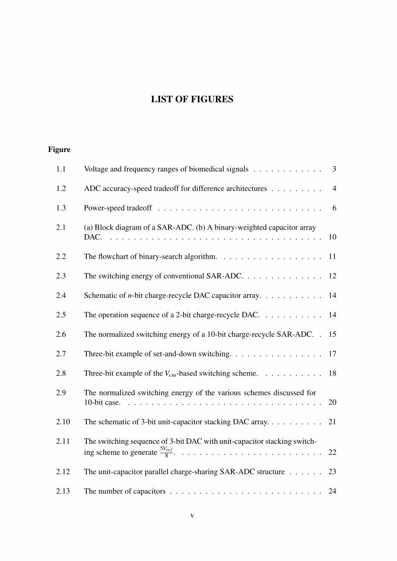
LIST OF FIGURES
Figure
1.1 Voltage and frequency ranges of biomedical signals . . . . . . . . . . . . 3
1.2 ADC accuracy-speed tradeoff for difference architectures . . . . . . . . . 4
1.3 Power-speed tradeoff . . . . . . . . . . . . . . . . . . . . . . . . . . . . 6
2.1 (a) Block diagram of a SAR-ADC. (b) A binary-weighted capacitor arrayDAC. . . . . . . . . . . . . . . . . . . . . . . . . . . . . . . . . . . . . 10
2.2 The flowchart of binary-search algorithm. . . . . . . . . . . . . . . . . . 11
2.3 The switching energy of conventional SAR-ADC. . . . . . . . . . . . . . 12
2.4 Schematic of n-bit charge-recycle DAC capacitor array. . . . . . . . . . . 14
2.5 The operation sequence of a 2-bit charge-recycle DAC. . . . . . . . . . . 14
2.6 The normalized switching energy of a 10-bit charge-recycle SAR-ADC. . 15
2.7 Three-bit example of set-and-down switching. . . . . . . . . . . . . . . . 17
2.8 Three-bit example of the Vcm-based switching scheme. . . . . . . . . . . 18
2.9 The normalized switching energy of the various schemes discussed for10-bit case. . . . . . . . . . . . . . . . . . . . . . . . . . . . . . . . . . 20
2.10 The schematic of 3-bit unit-capacitor stacking DAC array. . . . . . . . . . 21
2.11 The switching sequence of 3-bit DAC with unit-capacitor stacking switch-ing scheme to generate 5Vre f
8 . . . . . . . . . . . . . . . . . . . . . . . . . 22
2.12 The unit-capacitor parallel charge-sharing SAR-ADC structure . . . . . . 23
2.13 The number of capacitors . . . . . . . . . . . . . . . . . . . . . . . . . . 24
v

2.14 The switching sequence of an ideal 5-bit DAC with unit-capacitor parallelcharge-sharing switching scheme for Vin = 0.85Vre f . . . . . . . . . . . . . 24
2.15 (a) A typical single-stage dynamic comparator and (b) a two-stage dy-namic comparator. . . . . . . . . . . . . . . . . . . . . . . . . . . . . . . 27
2.16 Block diagram of a typical SAR logic. . . . . . . . . . . . . . . . . . . . 28
2.17 The conventional static DFF with asynchronous reset. . . . . . . . . . . . 28
2.18 The conventional static DFF with asynchronous set and reset. . . . . . . . 30
2.19 The switch buffers and the bottom plate parasitic capacitance. . . . . . . . 31
2.20 The theoretical power consumption of a conventional SAR ADC. . . . . . 33
2.21 The power breakdown of 10-bit SAR ADC. . . . . . . . . . . . . . . . . 33
2.22 The normalized power consumption of the capacitive DAC arrays at var-ious resolution. . . . . . . . . . . . . . . . . . . . . . . . . . . . . . . . 34
2.23 The normalized total power consumption of ADCs with different switch-ing schemes at various resolution. . . . . . . . . . . . . . . . . . . . . . 35
3.1 The proposed SAR-ADC structure. . . . . . . . . . . . . . . . . . . . . . 38
3.2 The complete switching sequence of a 3-bit DAC with the proposed switch-ing scheme. . . . . . . . . . . . . . . . . . . . . . . . . . . . . . . . . . 39
3.3 The simulated comparator output and DAC output voltage waveforms. . . 39
3.4 Simulated switching energy comparison of the three unit-capacitor arrayswitching schemes. . . . . . . . . . . . . . . . . . . . . . . . . . . . . . 41
3.5 (a) C3 was connected for charge sharing at time tm (b) C1 and C2 areconnected for charge sharing at time tn−1 (c) C1 and C3 are connected forcharge sharing at time tn. . . . . . . . . . . . . . . . . . . . . . . . . . . 42
3.6 (a) Channel charges injected into C1 and C2 when S2 is turned off. (b)Charges are attracted into the channel when S3 is turned on. . . . . . . . . 44
3.7 Conductances of the PMOS and NMOS switches. . . . . . . . . . . . . . 45
3.8 Comparison between analytical and simulation results . . . . . . . . . . . 46
vi
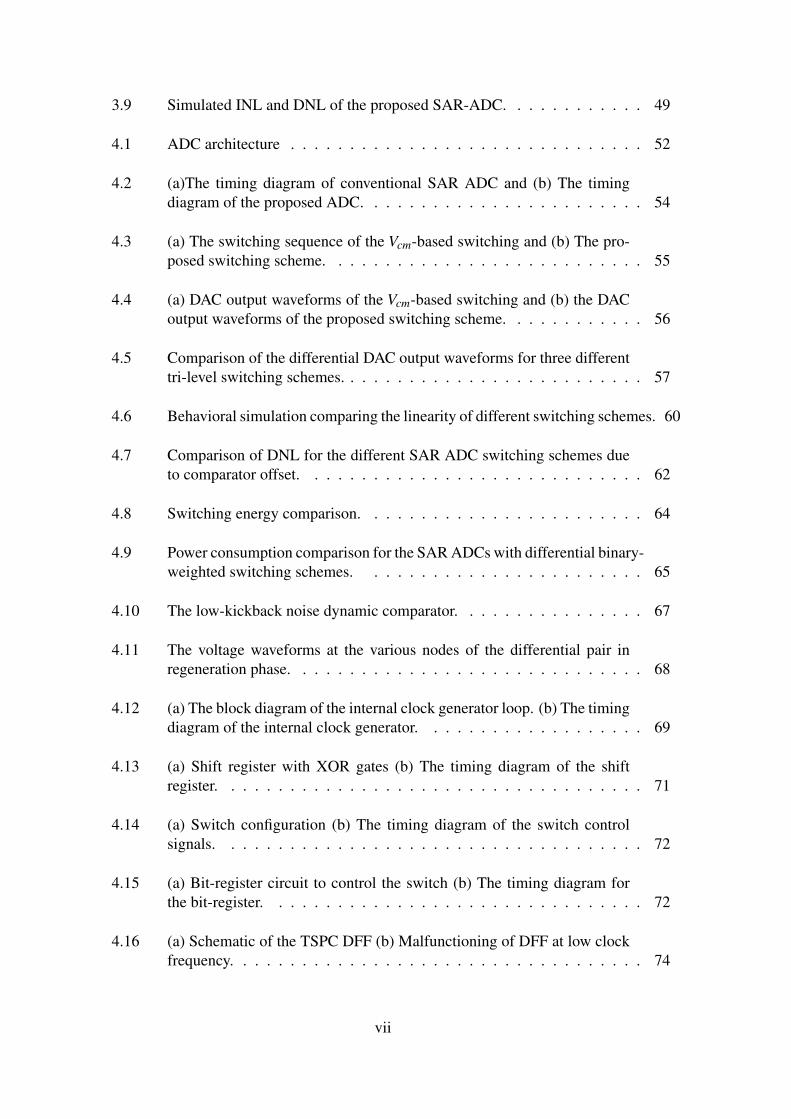
3.9 Simulated INL and DNL of the proposed SAR-ADC. . . . . . . . . . . . 49
4.1 ADC architecture . . . . . . . . . . . . . . . . . . . . . . . . . . . . . . 52
4.2 (a)The timing diagram of conventional SAR ADC and (b) The timingdiagram of the proposed ADC. . . . . . . . . . . . . . . . . . . . . . . . 54
4.3 (a) The switching sequence of the Vcm-based switching and (b) The pro-posed switching scheme. . . . . . . . . . . . . . . . . . . . . . . . . . . 55
4.4 (a) DAC output waveforms of the Vcm-based switching and (b) the DACoutput waveforms of the proposed switching scheme. . . . . . . . . . . . 56
4.5 Comparison of the differential DAC output waveforms for three differenttri-level switching schemes. . . . . . . . . . . . . . . . . . . . . . . . . . 57
4.6 Behavioral simulation comparing the linearity of different switching schemes. 60
4.7 Comparison of DNL for the different SAR ADC switching schemes dueto comparator offset. . . . . . . . . . . . . . . . . . . . . . . . . . . . . 62
4.8 Switching energy comparison. . . . . . . . . . . . . . . . . . . . . . . . 64
4.9 Power consumption comparison for the SAR ADCs with differential binary-weighted switching schemes. . . . . . . . . . . . . . . . . . . . . . . . 65
4.10 The low-kickback noise dynamic comparator. . . . . . . . . . . . . . . . 67
4.11 The voltage waveforms at the various nodes of the differential pair inregeneration phase. . . . . . . . . . . . . . . . . . . . . . . . . . . . . . 68
4.12 (a) The block diagram of the internal clock generator loop. (b) The timingdiagram of the internal clock generator. . . . . . . . . . . . . . . . . . . 69
4.13 (a) Shift register with XOR gates (b) The timing diagram of the shiftregister. . . . . . . . . . . . . . . . . . . . . . . . . . . . . . . . . . . . 71
4.14 (a) Switch configuration (b) The timing diagram of the switch controlsignals. . . . . . . . . . . . . . . . . . . . . . . . . . . . . . . . . . . . 72
4.15 (a) Bit-register circuit to control the switch (b) The timing diagram forthe bit-register. . . . . . . . . . . . . . . . . . . . . . . . . . . . . . . . 72
4.16 (a) Schematic of the TSPC DFF (b) Malfunctioning of DFF at low clockfrequency. . . . . . . . . . . . . . . . . . . . . . . . . . . . . . . . . . . 74
vii

4.17 Die micrograph and the layout of the proposed ADC. . . . . . . . . . . . 75
4.18 Measured DNL and INL. . . . . . . . . . . . . . . . . . . . . . . . . . . 76
4.19 8192-point FFT test spectrums for 5.3 kHz and 12.3 kHz input signals at25 kS/s. . . . . . . . . . . . . . . . . . . . . . . . . . . . . . . . . . . . 76
4.20 The dynamic performance. . . . . . . . . . . . . . . . . . . . . . . . . . 77
4.21 Measured SNDR at different sampling frequencies. . . . . . . . . . . . . 77
4.22 Power consumption breakdown of the ADC. . . . . . . . . . . . . . . . . 78
4.23 The pre-recorded neural spike signal and ADC output code. The X-axisis the normalized time in ms. The ADC output data are normalized to themid-code, 511, to align with the pre-recorded neural spike. . . . . . . . . 80
5.1 Architecture of the ADC with low-power digital controller. . . . . . . . . 84
5.2 (a) The timing diagram of the previous design and (b) The timing diagramof the new design. . . . . . . . . . . . . . . . . . . . . . . . . . . . . . . 85
5.3 (a) Top view of the customized MIM capacitor (b) Cross section view ofthe customized MIM capacitor. . . . . . . . . . . . . . . . . . . . . . . . 87
5.4 (a) Top view of the customized MOM capacitor (b) Cross section view ofthe customized MOM capacitor. . . . . . . . . . . . . . . . . . . . . . . 88
5.5 Floor plan for the capacitor array. . . . . . . . . . . . . . . . . . . . . . . 89
5.6 The high-speed low-leakage dynamic comparator. . . . . . . . . . . . . . 91
5.7 Layout of the comparator in (a) GF 65nm CMOS process and (b) UMC65nm CMOS. . . . . . . . . . . . . . . . . . . . . . . . . . . . . . . . . 92
5.8 Simulated comparator offset voltage mean and standard deviation at dif-ferent input common-mode voltage. . . . . . . . . . . . . . . . . . . . . 93
5.9 The internal clock generation and master reset circuitry. . . . . . . . . . . 94
5.10 The simplified timing diagram of the internal clock generation circuit. . . 95
5.11 The switch buffer design for the capacitor array. . . . . . . . . . . . . . . 95
5.12 Block diagram of the SAR logic controller. . . . . . . . . . . . . . . . . . 96
viii

5.13 The conceptual state machine of one-bit cycle. . . . . . . . . . . . . . . . 97
5.14 The timing diagram of one-bit cycle. . . . . . . . . . . . . . . . . . . . . 98
5.15 (a) The gate-level design of the main control circuit and (b) Transistorlevel implementation. . . . . . . . . . . . . . . . . . . . . . . . . . . . . 99
5.16 (a) Schematic of the dynamic latch for the DAC control logic (b) Thetiming diagram. . . . . . . . . . . . . . . . . . . . . . . . . . . . . . . . 99
5.17 The simulated 1024-point FFT output spectrum of ADC designed in GF65nm CMOS technology. . . . . . . . . . . . . . . . . . . . . . . . . . . 101
5.18 The simulated 2048-point FFT output spectrum of ADC designed in UMC65nm CMOS technology. . . . . . . . . . . . . . . . . . . . . . . . . . . 102
5.19 (a) ADC die photo and layout in GF 65nm CMOS design (b) ADC diephoto and layout in UMC process design. . . . . . . . . . . . . . . . . . 102
5.20 Measured FFT spectrum of the MIM capacitor ADC in GF process. . . . 103
5.21 Measured FFT spectrum of the MOM capacitor ADC in GF process. . . . 103
5.22 Measured INL and DNL at 1MS/s. The INL is obtained by best-fit line. . 104
5.23 8192-point FFT output spectrum for 44.7998 kHz and 490.6 kHz inputsignals. . . . . . . . . . . . . . . . . . . . . . . . . . . . . . . . . . . . 105
5.24 Dynamic performance at different input signal frequencies. . . . . . . . . 106
5.25 SNDR at different input signal frequencies for different sampling rates. . 107
5.26 The ENOB, power consumption and FoM for different sampling rates. . . 107
5.27 Overview of state-of-the-art SAR ADCs power efficiency versus speed. . 110
5.28 Overview of state-of-the-art SAR ADCs area versus power efficiency. . . 111
A.1 The switching sequence of a 2-bit CR SAR-ADC . . . . . . . . . . . . . 117
A.2 The bottom-plate of a capacitor is switched from V1 bottom to V2 bottomduring a switching transition. . . . . . . . . . . . . . . . . . . . . . . . . 118
C.1 (a) Effect of charge injection in a sampling circuit, (b) Addition of dummydevice to reduce charge injection. . . . . . . . . . . . . . . . . . . . . . . 128
ix

C.2 (a) The proposed DAC schematic with parasitic capacitance, (b) TG switchturning on . . . . . . . . . . . . . . . . . . . . . . . . . . . . . . . . . . 129
C.3 TG switch with dummy transistors on both sides . . . . . . . . . . . . . . 130
C.4 TG switch with dummy transistors close to DAC output . . . . . . . . . . 133
C.5 TG switch with dummy transistors close to unit capacitor . . . . . . . . . 133
C.6 SPICE simulated error voltage for different switch configurations . . . . . 134
D.1 Swtich S2 turning off. . . . . . . . . . . . . . . . . . . . . . . . . . . . . 135
D.2 Swtich S3 turning on. . . . . . . . . . . . . . . . . . . . . . . . . . . . . 137
x

LIST OF TABLES
Table
1.1 Comparison of different types of biomedical signals . . . . . . . . . . . . 3
2.1 Comparison of different switching schemes for 10-bit case . . . . . . . . 20
2.2 Switching activity of each logic gate in the static DFF with asynchronousreset . . . . . . . . . . . . . . . . . . . . . . . . . . . . . . . . . . . . . 29
3.1 Input voltage and the corresponding switching energy consumption . . . . 41
3.2 Comparison of simulated power consumption . . . . . . . . . . . . . . . 47
3.3 Comparison of hardware and conversion time . . . . . . . . . . . . . . . 48
4.1 Comparison of different switching schemes for 10-bit cases . . . . . . . . 64
4.2 Summary of performance . . . . . . . . . . . . . . . . . . . . . . . . . . 79
4.3 Comparison to State-of-the art SAR ADCs . . . . . . . . . . . . . . . . . 79
5.1 Extracted capacitors and their normalized value . . . . . . . . . . . . . . 89
5.2 Measured ADC Power and FoM at different sampling frequencies . . . . 108
5.3 Simulated Power Consumption at 1 MS/s . . . . . . . . . . . . . . . . . 108
5.4 Specification summary . . . . . . . . . . . . . . . . . . . . . . . . . . . 109
5.5 Comparison to State-of-the art . . . . . . . . . . . . . . . . . . . . . . . 110
C.1 UMC 65nm CMOS process device parameters . . . . . . . . . . . . . . . 131
C.2 Comparison of Theoretical calculations and SPICE simulation results . . 132
D.1 Summary of TG switch charge-injection . . . . . . . . . . . . . . . . . . 140
xi
D.2 8 combinations of NMOS and PMOS in TG for determining charge in-jection . . . . . . . . . . . . . . . . . . . . . . . . . . . . . . . . . . . . 141
xii

LIST OF ABBREVIATIONS
EEG Electroencephalogram
ECG Electrocardiogram
EMG Electromyogram
ADC Analog-to-Digital Converter
DAC Digital-to-Analog Converter
SAR Successive Approximation Register
POC Point-of-Care
ENG Electroneurogram
OpAmp Operational Amplifier
MDAC Multiplying Digital-to-Analog Converter
FoM Figure-of-Merit
SNDR Signal-to-Noise and Distortion Ratio
MSB Most Significant Bit
LSB Least Significant Bit
S/H Sample-and-Hold
CR Charge-Redistribution
DFF D Flip-Flop
TSPC True Single Phase Clock
TG Transmission Gate
SNR Signal-to-Noise Ratio
DNL Differential Non-Linearity
xiii

INL Integral Non-Linearity
MUX Multiplexer
MOM Metal-Oxide-Metal
MIM Metal-Insulator-Metal
xiv

ABSTRACT
The ever increasing healthcare cost has become a burden for modern society. Recently,
a lot of research activities have been carried out in search of innovative and low-cost solu-
tions for the healthcare industry. Benefited from advanced submicron CMOS technologies,
which allow a high level of integration and reduction of cost, many miniaturized biomedical
devices were developed for different applications. The biopotential signals, such as Elec-
troencephalogram (EEG), Electrocardiogram (ECG) and Electromyogram (EMG), were
recorded and studied with customized CMOS devices. These low-cost portable CMOS
based biomedical devices operating at low supply voltage, which can be battery-powered,
will be able to replace the conventional lab-based bulky diagnosis or monitoring systems in
the near future. In a typical biomedical acquisition and monitoring system, the biomedical
signals, which could be in the form of pressure, PH value, nerve stimulus, or electrical
potentials, are usually sensed by single or multi-channel sensors, amplified by a low-pass
or bandpass amplifier, digitized by an ADC and then transmitted to the data processing
unit. One of the most critical and power consuming components in such system is the
ADC. Therefore, minimizing the power consumption is a crucial design target for ADC in
biomedical applications.
The Successive Approximation Register (SAR) ADC exhibits significant advantages
compared to other ADC architectures such as pipelining and Delta-Sigma, in terms of
power consumption and area. Two distinct types of SAR ADCs, namely the unit-capacitor
array SAR ADC and binary-weighted capacitor SAR ADC, were studied and analyzed in
this report. The unit-capacitor array ADC has theoretically the lowest DAC power con-
sumption. However, the digital circuit overhead is large. Two binary-weighted capacitor
SAR ADCs were designed and implemented. A novel tri-level switching algorithm that
xv

allows 97% Digital-to-Analog Converter (DAC) power reduction and 75% area savings is
also proposed. Customized digital logic circuit offers variable sampling rates for different
applications and also further reduce ADC power up to 50%.
xvi
Chapter 1
Introduction
The healthcare industry has been expanding tremendously year on year. Governments
worldwide are struggling to pay for healthcare. It is reported that the total healthcare ex-
penditures in the developed countries are estimated to be over 7.5 trillion dollars by 2020,
up from 5 trillion dollars in 2010 [1]. The global healthcare spending is expected to double
by 2050, if current trends hold [2]. Many factors account for the ever increase in the global
healthcare costs. One of the main reasons is the aging of world population. The world
population aged over 60 years was about 10% in 2000, and it will be more than 21% by
2015 [2, 3]. Studies show that elderly people suffer from chronic diseases more often, and
require 3 to 5 times more healthcare service than younger people due to new and more ex-
pensive treatments. The unprecedented world population aging [3] not only slows down the
economy growth, but also drastically increases the public expenditure, of which healthcare
is the largest portion. In this aspect, low-cost biomedical devices are in great demand.
In the last years, there has been a promising trend in the design of CMOS based biomed-
ical signal acquisition systems. These biomedical systems can be used for real-time moni-
toring, detection, prevention and diagnosis of many diseases with greater convenience. Si-
multaneously merging the integrated circuit technology capabilities with clinical demands,
portable and miniaturized biomedical devices were designed to drive the development of
reliable Point-of-Care (POC) diagnostic systems. These POC systems are expected to rev-
olutionize the healthcare industry. For example, the Frost & Sullivan recognized POC sys-
1

tem provider, Radisens Diagnostics [4], has developed a single connected multi-diagnostic
POC device, which requires only a finger prick of blood and the clinical results can be
delivered within minutes of blood draw.
1.1 Biomedical Signals
Most living organisms, like our human body, consist of many component systems, such
as the nervous system, the cardiovascular system and musculoskeletal system. Each sys-
tem is also made up of some subsystems that can carry different physiological activities.
For example, the respiratory system introduces oxygen to the interior and performs gas ex-
change. Physiological processes are complex in nature and require different organs in the
human body to function simultaneously. Most of the physiological processes are accompa-
nied by, or manifest themselves as, signals that reflect their nature and activities [5]. Such
signals could be of many types, including biochemical in the form of hormones and neuro-
transmitters, electrical signal in the form of potential or current, and physical signal such as
pressure or temperature [5]. In the human body, the various neuronal electrical signals are
very important in clinical diagnosis, care monitoring, therapy and research including Elec-
troneurogram (ENG) signal, EMG, ECG, EEG and so on. Biomedical signals are usually
characterized as low frequency ranges (few tens of kHz) and small voltage amplitudes (∼
mV) [5]. Table 1.1 shows a comparison of different biomedical signals in the human body,
with their location and signal characteristics as well as the pick-up electrode. In order to
acquire these signals and process them in the digital domain, ADCs are needed in these
systems. The common requirements for ADC in biomedical applications include moderate
speed, usually less than 200 kS/s, modest resolution of 8 to 10-bit [6, 7], low-voltage and
low-power, and small-area in some applications such as bio-implantable devices.
Figure 1.1 below shows a direct graphical comparison of some conventional biomedical
signals in the human body in terms of voltage amplitude and signal frequency [9]. It can
be seen that these signals have a dynamic range from tens of µV to tens of mV and cover
the frequency range from 0.05 Hz to 10 kHz.
2

Table 1.1: A comparison of different types of biomedical signals from the human body [5][8]
BiomedicalSignals
Location Amplitude Bandwidth Electrode
ENG Stimulus over anerve
3 - 10 µV 1-10 kHz Needle electrode
EMG Skeletal muscle 1 - 10 mV 1 Hz - 3 kHz surface electrode/glass micropipete
ECG Heart 0.1 - 1 mV 0.05 - 100 Hz Surface electrodeEEG Brain 10 - 100 µV 0.5 - 100 Hz Surface electrodeEOG Retina 15 - 200 µV DC-38 Hz Surface electrode
0.1 1 10 100 1k 10k0.01
10µ
100µ
1m
10m
100m
Volt
age
(V)
frequency (Hz)
EOG
ECG
EEG
EMG
Figure 1.1: Voltage and frequency ranges of some conventional biomedical signals [9].
3
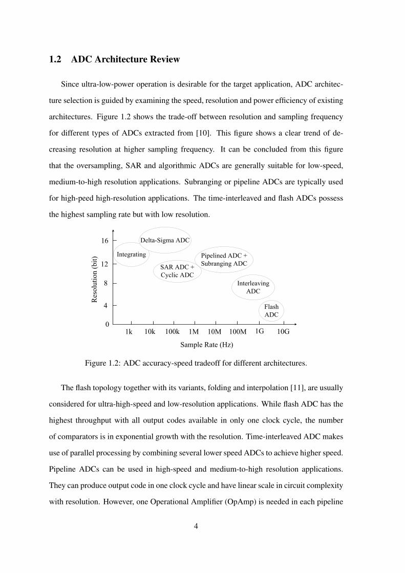
1.2 ADC Architecture Review
Since ultra-low-power operation is desirable for the target application, ADC architec-
ture selection is guided by examining the speed, resolution and power efficiency of existing
architectures. Figure 1.2 shows the trade-off between resolution and sampling frequency
for different types of ADCs extracted from [10]. This figure shows a clear trend of de-
creasing resolution at higher sampling frequency. It can be concluded from this figure
that the oversampling, SAR and algorithmic ADCs are generally suitable for low-speed,
medium-to-high resolution applications. Subranging or pipeline ADCs are typically used
for high-peed high-resolution applications. The time-interleaved and flash ADCs possess
the highest sampling rate but with low resolution.
0
Res
olu
tion
(bit
)
4
8
12
16
1k 10k 100k 1M 10M 100M 1G 10G
Sample Rate (Hz)
Integrating
Delta-Sigma ADC
SAR ADC +
Cyclic ADC
Pipelined ADC +
Subranging ADC
Flash
ADC
Interleaving
ADC
Figure 1.2: ADC accuracy-speed tradeoff for different architectures.
The flash topology together with its variants, folding and interpolation [11], are usually
considered for ultra-high-speed and low-resolution applications. While flash ADC has the
highest throughput with all output codes available in only one clock cycle, the number
of comparators is in exponential growth with the resolution. Time-interleaved ADC makes
use of parallel processing by combining several lower speed ADCs to achieve higher speed.
Pipeline ADCs can be used in high-speed and medium-to-high resolution applications.
They can produce output code in one clock cycle and have linear scale in circuit complexity
with resolution. However, one Operational Amplifier (OpAmp) is needed in each pipeline
4

stage and the number of stages is usually equal to the resolution. These OpAmps that
are working in closed-loop to form the Multiplying Digital-to-Analog Converter (MDAC)
must have high gain and wide bandwidth. As a result, the power consumption is large.
The oversampling ADC, algorithmic ADC and integrating ADC also have one or more
OpAmps. In modern deep sub-micron CMOS process, a high gain OpAmp is difficult to
design because the intrinsic gain of a single transistor is small due to short-channel effect.
In addition, the scaling down of the supply voltage has also reduced transistor headroom,
thus limiting the conventional design techniques such as cascoding. Therefore, these ADCs
are also not suitable architectures for low-power ADC design.
A widely adopted metric to compare ADCs across power and speed is the Figure-of-
Merit (FoM) [11]
FoM =P
2ENOB ·2ERBW(1.1)
where P is the power consumption, ENOB is the effective number of bits of the ADC, and
ERBW is the effective resolution bandwidth, defined as the input signal frequency at which
the Signal-to-Noise and Distortion Ratio (SNDR) drops by 3dB from its low frequency
value.
The Charge-Redistribution (CR) SAR ADC first presented in [12] can be realized by
a capacitive DAC, a comparator and SAR logic. The capacitive DAC output is compared
against the sampled input voltage by the comparator, whose output is processed by the
digital logic that in turn drives the DAC. The SAR algorithm uses binary search to ap-
proximate the analog input with digital output, generating one bit at one clock cycle [13].
The DAC usually consists of a binary-weighted capacitor array, which also serves as the
sampling capacitor. The comparator can be implemented by a dynamic latch, which does
not consume any DC power. The SAR logic and switches are standard sequential circuits
and MOS switches, respectively. This simple structure and the elimination of static cur-
rent make SAR ADC a very popular architecture for power constraint and low-to-medium
speed circuits.
Figure 1.3 shows the FoM plotted against sampling frequency for various ADC archi-
5

tectures. The ADCs shown in the plot are extracted from the publications in the Interna-
tional Solid-State Circuit conference (ISSCC) from 1997 to 2013 [14]. The best ADC has
FoM lower than 10fJ/conversion-step, which was achieved by SAR ADC in 2013. In gen-
eral, the SAR ADCs are designed for low-to-medium speed applications and have a lower
FoM than other types of ADCs. In addition, the FoM is also relatively independent of the
ADC sampling rate. Compared to other types of ADCs, SAR ADC offers the best energy
efficiency in the target frequency range.
106
108
1010
100
101
102
103
104
105
Sampling rate (S/s)
FO
M (
fJ/C
−S
)
FlashFoldingPipelineSARΣ−∆
Figure 1.3: Power efficiency and speed tradeoff for different ADC architectures in litera-ture.
1.3 Motivation
As discussed in previous sections, the advanced CMOS technology today allows us
to design the next generation healthcare and monitoring systems, which are capable of
long-term monitoring and early detection of abnormalities. The CMOS-based biomedical
systems improve the quality of people’s lives by providing competitive or better medical
service than the conventional way while reducing the medical costs. For instance, hand-
held devices can be used at home for monitoring purpose. This will save time and cost for
the patients. Some patients with chronic diseases may not need to visit the specialists for
6

consultation on a regular frequent basis. This can release the equipment in the hospital for
better utilization. In addition, the specialists could also focus on those patients who need
more care and attention. Both patients and doctors could benefit from these systems.
Motivated by the advantages of the portable biomedical devices as well as the huge
demand for cost-effective healthcare systems, this work concentrates on the design of ultra-
low-power ADCs by searching for new techniques and circuit structures for biomedical
systems, especially for brain neural signal recording.
1.4 Thesis Contribution
This thesis focuses on the design of ultra-low power, moderate resolution, low-to-
medium speed ADCs for biomedical applications. SAR ADC has been demonstrated with
highest energy efficiency in literature. By exploring new methods to minimize the power
consumption in SAR ADCs, a number of contributions have been achieved:
Unit capacitor sampling: A unit-capacitor array sampling technique was proposed to trade
off speed and power consumption. Theoretical analysis of the unit-capacitor sam-
pling technique shows excellent power consumption performance over other switch-
ing schemes. The capacitive DAC output accuracy was also analyzed.
Tri-level switching: A novel tri-level switching scheme based on binary-weighted capac-
itor arrays was presented. The switching energy of the proposed tri-level switching
is the lowest compared to existing switching schemes. Besides the power reduction,
the capacitive DAC area is also reduced by 75%.
Dynamic Power Reduction in Digital Circuits: A dynamic latch-based digital controller
was proposed to reduce the digital overhead for the tri-level SAR ADC. Simulation
results show that the SAR logic controller power is reduced by 5 times compared to
conventional design.
7

1.5 Thesis Organization
This thesis is organized as follows. Chapter 1 introduces the biomedical signals and
gives an overview on various ADC architectures. Motivations were drawn from the discus-
sion. The contributions of this work are also discussed.
Chapter 2 reviews the fundamentals of CR SAR ADC architecture. The conventional
binary-weighted switching scheme is presented and analyzed. In addition, several methods
to reduce the switching energy are also discussed in detail.
Chapter 3 presents the proposed unit-capacitor DAC array switching scheme. The non-
idealities of the proposed scheme is analyzed and discussed. Some simulation results of
the ADC are shown.
Chapter 4 presents a low-power SAR ADC prototype with novel tri-level binary-weighted
capacitor array switching scheme. The proposed switching scheme is compared against
other switching schemes in terms of power consumption, area, and linearity performance.
Measurement results show that the proposed SAR ADC achieves comparable FoM com-
pared to some other state-of-the-art SAR ADCs despite a mistake made during the design
phase. The power reduction capability of the proposed switching scheme is validated.
Chapter 5 focuses on reducing power consumption in the digital circuit by customiza-
tion. Experimental results reveals that the proposed digital controller circuit is 50% more
energy-efficient than the previous design.
In chapter 6, conclusions are drawn. Some future works on the design of ultra-low-
power SAR ADC for biomedical interface IC are also discussed.
8

Chapter 2
Low-Power SAR ADC Architecture
Review and Power Analysis
As discussed in the previous chapter, SAR ADC is very popular due to its low power na-
ture [7, 15, 16]. In this chapter, the conventional SAR ADC is introduced in the beginning,
followed by some low-power SAR ADC switching schemes. The low-power switching
schemes are divided into two categories. One type is the binary-weighted capacitor array
switching scheme and the other type is based on unit-capacitor array switching. In lit-
erature, the comparison for different binary-weighted SAR ADC switching schemes only
considered the switching energy from the capacitor arrays. This is necessary but incom-
plete. The power consumption from other components of the ADC, especially the SAR
logic circuit, should also be considered for a fair comparison. In the later part of this chap-
ter, a detailed power consumption model for conventional SAR ADC is built. Based on
the conventional SAR ADC power model, the complete power comparison for differential
binary-weighted switching schemes is illustrated. The unit-capacitor switching schemes
are based on ultra low-energy unit-capacitor DAC arrays, and their theoretical switching
energy consumptions are much lower than the binary-weighted ones. Two unit-capacitor
DAC switching schemes are discussed after the binary-weighted capacitor array switching
schemes in this chapter.
9

2.1 Conventional CR SAR ADC
A conventional CR SAR-ADC can sequentially produce the equivalent digital output
codes of a sampled analog voltage by means of binary-search [13]. The binary search
algorithm determines each output bit serially from the Most Significant Bit (MSB) to the
Least Significant Bit (LSB). As shown in Figure 2.1 (a), a conventional single-ended CR
SAR ADC is made up of a comparator, a capacitive DAC, a Sample-and-Hold (S/H) circuit
and the SAR logic. An n-bit DAC array shown in Figure 2.1 (b) consists of n+1 binary-
weighted capacitors, having a total capacitance of 2nC0, where C0 is the unit capacitor. The
output voltage of the capacitive DAC at any moment is given by:
VDAC =CH
CH +CLVre f (2.1)
where CH is the sum of all the capacitors connected to reference voltage, CL is the sum of
all the capacitors connected to ground and Vre f is the reference voltage.
Vref
...
VDAC
C0C02n-2C02n-1C0
Clk
DAC
Vin
Comparator
SA
R
Digital
output
S/H
(a)
(b)
VDAC
[b0,b1,…,bn-1]
bn bn-1 b1
Figure 2.1: (a) Block diagram of a SAR-ADC. (b) A binary-weighted capacitor array DAC.
10

2.1.1 Basic Operation of Conventional CR SAR ADC
The operation of SAR ADC is binary-search and described as follows [13]. The con-
version begins by sampling the analog input signal on a S/H circuit. At the same time all
the capacitors are reset to ground. Next, the digital control circuit sets the MSB to “1” and
other bits to “0”. The digital word is applied to the DAC and the largest capacitor is con-
nected to Vre f while the remaining capacitors are unchanged. As a result, a voltage of Vre f2
appears at the DAC output. The comparator is then triggered and the sampled analog volt-
age is compared with the DAC output voltage. If the comparator output is high, the MSB
is latched to “1”. Otherwise, the MSB is latched to “0”. After the first step in approxima-
tion, the MSB is stored in a register and the second MSB is set to “1”. The approximation
process continues to determine the subsequent bit. The process continues in this manner
until all bits are decided by the binary-search. A flowchart of the binary search algorithm
is shown in Figure 2.2.
Sampling Vin;
Reset VDAC=0;
b1,…,bN-1,bN=0;
Stop
YesNo
n=n+1n=n+1
For n-th
bit, bn=1
bn=0;
If n = N
Yes
NoNo
Yes
bn=1;
If n = NVin>VDAC
Figure 2.2: The flowchart of binary-search algorithm.
11

2.1.2 Switching Energy
A detailed analysis of the switching energy can be found in Appendix A. The average
switching energy of conventional single-ended SAR ADC can be derived as [17]:
Eavg conv =n
∑i=1
2n−2i (2i −1)
C0V 2re f (2.2)
The MATLAB simulation of a 10-bit conventional SAR-ADC switching energy is
shown in Figure 2.3. The input analog signal is swept from 0 to full scale and the switching
energy for each output digital code is calculated. The energy is normalized to CV 2re f . The
average switching energy is 681.67CV 2re f . It should be noted that the derivation and simu-
lation shown here are for single-ended ADC. For fully-differential structure, the switching
energy should be doubled.
0 200 400 600 800 1000300
400
500
600
700
800
900
Output code
Nor
mal
ized
sw
itchi
ng e
nerg
y
Figure 2.3: The switching energy of conventional SAR-ADC.
2.2 Low-power Binary-weighted DAC Capacitor Array Switching Schemes
Review
The DAC capacitor arrays in conventional SAR ADC are the main source of power
consumption, and the total capacitance is exponentially proportional to resolution. In
12

other words, as the ADC resolution increases, the capacitance increases exponentially,
which implies the power consumption also increases exponentially. In addition to that,
the conventional SAR ADC switching algorithm is energy-inefficient during the “down”-
transition [18]. In this section, several switching schemes that are based on the binary-
weighted capacitor array to reduce the power consumption are discussed.
2.2.1 The Charge-recycle Switching Scheme
The conventional switching algorithm has been shown to be energy-inefficient, espe-
cially in a “down” transition. An “up” transition refers to the charging of the next largest
capacitor to Vre f when the sampled input signal is larger than the DAC output in the pre-
vious clock cycle. A “down” transition means when the sampled input voltage is less than
the DAC output voltage in the previous clock cycle, the larger capacitor that was connected
to Vre f in the previous clock is now discharged to ground and the next largest capacitor in
turn is connected to Vre f . Therefore, a large amount of energy is drawn from the reference
voltage in order to inverse the polarity of both the larger and smaller capacitors.
The charge-recycle switching algorithm [18] [19] avoids discharging the larger capaci-
tor to ground in a “down” transition, therefore, less energy is required. The schematic n-bit
capacitive DAC with the charge-recycle switching algorithm is shown in Figure 2.4. The
total capacitance is 2nC0, which is the same as that of the conventional switching algorithm.
The MSB capacitor, which is the largest capacitor in the conventional DAC, is split into a
binary-weighted sub-array. Therefore, the MSB array and the remaining LSB array are
identical.
The operation of the charge-recycle switching algorithm can be illustrated by the switch-
ing sequence of a 2-bit DAC as shown in Figure 2.5. The main difference between the
charge-recycle switching scheme and the conventional one is in the “down” transition. For
the 2nd MSB conversion shown in Figure 2.5, no capacitor is charged from ground to Vre f
during the “down” transition. Only the largest capacitor in the MSB array capacitor is
discharged from Vre f to ground.
13

...
VDAC
C0C02n-3
C02n-2
C0
... C02n-3
C02n-2C0
Vref
Vref
C0
LSB Array
MSB Array
Figure 2.4: Schematic of n-bit charge-recycle DAC capacitor array.
C C
VDAC=0 VDAC=1
2
3
4
1
4
B1=1
B1=0C C
C C
C C
Vref
VDAC=
C CVref
C C
Vref
VDAC=
C C
C C
Vref
SamplingMSB
conversion2
ndMSB
“up”
“down”
Figure 2.5: The operation sequence of a 2-bit charge-recycle DAC.
14

The switching energy for the 2-bit DAC shown in Figure 2.5 can be determined by the
following equations:
Eup =(−Vre f
)2C[(
3Vre f
4−Vre f
)−(
Vre f
2−Vre f
)]+(−Vre f
)C[(
3Vre f
4−Vre f
)−(
Vre f
2−0)]
=CV 2
re f
4(2.3)
Edown =(−Vre f
)C[(
Vre f
4−Vre f
)−(
Vre f
2−Vre f
)]=
CV 2re f
4(2.4)
The switching energy in a “up” transition is the same as that for conventional DAC. The
switching energy of charge-recycle in a “down” transition given by (2.4) is much smaller
than that for the conventional DAC, which is5CV 2
re f4 . The MATLAB simulation of a 10-bit
charge-recycle SAR-ADC switching energy is shown in Figure 2.6. The average switching
energy is 426.17CV 2re f , which implies a 37.5% saving as compared with the conventional
switching algorithm.
0 200 400 600 800 1000300
400
500
600
700
800
900
Output code
Nor
mal
ized
ene
rgy
(C 0Vre
f2
)
conventionalcharge−recycle
Figure 2.6: The normalized switching energy of a 10-bit charge-recycle SAR-ADC.
The main problem with the charge-recycle switching scheme is the digital overhead.
Since the MSB array and the LSB array are identical and independently switched, ad-
ditional bit-registers are needed to control the switches of the MSB capacitor array. The
increased digital circuit power consumption might overweight the power saving in the DAC
15
capacitor arrays. In addition, the number of switches is almost doubled. Hence, the ADC
area is increased compared with the conventional one.
2.2.2 The Set-and-down Switching Scheme
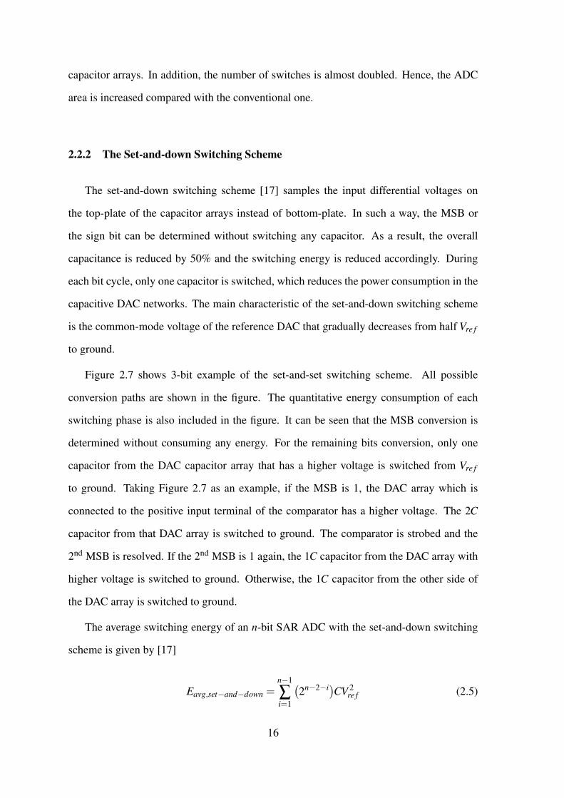
The set-and-down switching scheme [17] samples the input differential voltages on
the top-plate of the capacitor arrays instead of bottom-plate. In such a way, the MSB or
the sign bit can be determined without switching any capacitor. As a result, the overall
capacitance is reduced by 50% and the switching energy is reduced accordingly. During
each bit cycle, only one capacitor is switched, which reduces the power consumption in the
capacitive DAC networks. The main characteristic of the set-and-down switching scheme
is the common-mode voltage of the reference DAC that gradually decreases from half Vre f
to ground.
Figure 2.7 shows 3-bit example of the set-and-set switching scheme. All possible
conversion paths are shown in the figure. The quantitative energy consumption of each
switching phase is also included in the figure. It can be seen that the MSB conversion is
determined without consuming any energy. For the remaining bits conversion, only one
capacitor from the DAC capacitor array that has a higher voltage is switched from Vre f
to ground. Taking Figure 2.7 as an example, if the MSB is 1, the DAC array which is
connected to the positive input terminal of the comparator has a higher voltage. The 2C
capacitor from that DAC array is switched to ground. The comparator is strobed and the
2nd MSB is resolved. If the 2nd MSB is 1 again, the 1C capacitor from the DAC array with
higher voltage is switched to ground. Otherwise, the 1C capacitor from the other side of
the DAC array is switched to ground.
The average switching energy of an n-bit SAR ADC with the set-and-down switching
scheme is given by [17]
Eavg,set−and−down =n−1
∑i=1
(2n−2−i)CV 2
re f (2.5)
16
0Vip – Vin >0?
CVref2
CVref2
Vip – Vin>Vref/2?
0.25CVref2
0.75CVref2
0.75CVref2
0.25CVref2
Vip – Vin >-
Vref/2?
Vip – Vin >
-0.25Vref?
CC2C
CC2C
Vip
Vin
Vref
Vref Vref
Vref
CC2C
CC2C
CC2C
CC2C
Vref
Vref
CC2C
CC2C
Vref
Vref
Vip – Vin>0.75Vref?
CC2C
CC2C
Vref
Vref
Vip – Vin>0.25Vref?
Vref Vref
CC2C
CC2C
Vref
CC2C
CC2C
VrefVref
Vref
Vip – Vin >
-0.75Vref?
CC2C
CC2C
Vref
Vref
Figure 2.7: Three-bit example of set-and-down switching.
For a 10-bit ADC with the set-and-down switching scheme, the energy drawn from
reference voltage is 255CV 2re f , which is 81% less than that of the conventional one. Nev-
ertheless, this amount of power saving is for the DAC capacitor arrays only. Indeed, the
SAR logic circuit power consumption of the set-and-down SAR ADC is increased com-
pared with the conventional SAR ADC. The simplified digital control circuits discussed
in [17] include a 10-bit shift register, and two rows of bit-registers to control the switch
buffers. Each element in the bit-register consists of a DFF, a delay buffer and a AND gate.
The set-and-down SAR ADC requires 50% more D Flip-Flops (DFFs) in the digital control
circuit as well as some additional logic gates, as compared to the conventional counterpart.
2.2.3 Vcm-based switching scheme
The Vcm-based switching scheme [20] determines the sign of the differential input sig-
nal by top-plate sampling technique to reduce DAC capacitor arrays area and switching
power. This is similar to the set-and-down switching scheme except that the bottom-plate
of the differential arrays are connected to Vcm. For the remaining bit conversion phases, the
switching from both capacitor arrays are complimentary. Therefore, the differential DAC
17

output voltages are symmetrical around the input common-mode voltage, Vcm. As a result,
the comparator offset voltage has insignificant effect on the ADC linearity.
Figure 2.8 shows the conversion procedure of a 3-bit differential capacitive DAC arrays
performing the Vcm-based switching scheme. The operation is explained as follows. In
the sampling phase ϕ1, the differential input voltages are sampled on the top-plate of the
capacitive DAC arrays. Meanwhile, the bottom-plates are connected to the Vcm. During
phase ϕ2, the comparator determines the MSB. If MSB is “1”, the DAC voltage on the
positive input terminal of the comparator needs to be reduced and the other DAC voltage
on the negative input terminal of the comparator needs to be increased. Therefore, the 2C
capacitor on the higher voltage capacitor array is switched to ground and the 2C on the
lower voltage capacitor array is connected to Vre f . If MSB is “0”, the switching procedure
is reversed.
0Vip – Vin >0?
0.5CVref2
0.5CVref2
Vip – Vin
>Vref/2?
0.125CVref2
0.625CVref2
0.625CVref2
0.125CVref2
Vip – Vin >-
Vref/2?
Vip – Vin>
0.75Vref?
Vip – Vin>
0.25Vref?
Vip – Vin >
-0.25Vref?
Vip – Vin >
-0.75Vref?
Sampling
phase Φ11st -bit, Φ2 2nd -bit, Φ3
3rd -bit, Φ4
Vcm
Vcm
CC2C
CC2C
CC2C
CC2C
Vip
Vin
Vcm
Vcm
CC2C
CC2C
Vcm
Vcm
Vref
CC2C
CC2C
Vcm
VcmVref
CC2C
CC2C
Vcm
Vcm
Vref
CC2C
CC2C
Vcm
VcmVref
Vcm
CC2C
CC2C
VcmVref
Vref
Vref Vcm
CC2C
CC2C
VcmVref
Figure 2.8: Three-bit example of the Vcm-based switching scheme.
For a 10-bit SAR ADC with Vcm-based switching scheme, the average switching en-
ergy is derived as 170.4CV 2re f , which is 87% reduction from the conventional switching
algorithm. A generalized formula to calculate the average switching energy of an n-bit
18

Vcm-based SAR ADC is given below [21]:
Eavg,Vcm−based =n−1
∑i=1
2n−2−2i (2i −1)CV 2
re f (2.6)
Although one more control signal is needed for each capacitor to control the switch
to Vcm, the Vcm-based switching scheme does not require extra DFF in the digital con-
trol logic. The reason is that switching in the two capacitor arrays is complementary,
which is the same as the conventional switching scheme. Hence, the Vcm-based switch-
ing scheme decreases DAC capacitor arrays switching power without introducing digital
overhead. Nevertheless, new switching schemes needs to be explored for further power
savings.
2.2.4 Summary of binary-weighted DAC array switching schemes
For the four binary-weighted capacitor array switching schemes discussed above, a
comparison of the switching energy of 10-bit fully differential ADC is shown in Figure
2.9. It shows the amount of energy required in the DAC arrays for the ADC to generate the
corresponding output code. It is clear that the Vcm-based switching scheme has the largest
energy saving among all the binary-weighted DAC capacitor array switching schemes.
Table 2.1 shows a comparison of different binary-weighted switching schemes in terms
of average switching energy, capacitor area saving and the number of DFFs in the SAR
logic circuit. The charge-recycle and set-and-down switching schemes reduce the DAC
capacitor array switching power but introduce digital overhead. The Vcm-based switching
scheme has the largest power saving without adding digital circuit complexity, making it
the most power-efficient switching scheme among the four.
2.3 Low-power Unit-capacitor DAC Array Switching Schemes Review
The previous section focuses on the binary-weighted capacitor DAC array switching
schemes. The binary-weighted capacitor array consumes power in every switching activ-
19

0 200 400 600 800 10000
200
400
600
800
1000
1200
1400
1600
1800
2000
Digital code
Sw
itchi
ng E
nerg
y (C
V ref
2)
ConventionalCharge−recycleSet−and−downV
cm−based
Figure 2.9: The normalized switching energy of the various schemes discussed for 10-bitcase.
Table 2.1: Comparison of different switching schemes for 10-bit case
Switching energySwitching schemes
(CV 2re f )
Energy saving Area saving No. of DFFs
Conventional [13] 1363.33 Ref. Ref. 2nCharge-recycle [18] 852.34 37.48% 0% 3(n−1)Set-and-down [17] 255.5 81.26% 50% 3n
Vcm-based [20] 170.16 87.52% 50% 2n
20

ity. There is another type of capacitor DAC array that is made up of a group of unit ca-
pacitors. The unit-capacitor DAC array makes use of the passive charge-sharing and does
not consume power in every switching step. It only needs to charge up some capacitors to
the reference voltage when necessary. In this section, two switching schemes based on the
unit-capacitor DAC array are reviewed.
2.3.1 Unit-capacitor Stacking Scheme
This unit-capacitor stacking method is proposed in [22]. With the unit-capacitor stack-
ing scheme, only one unit capacitor is charged to Vre f in every conversion cycle. The unit-
capacitor stacking switching scheme can reduce the switching energy to the theoretical
lowest limit, which is 0.5CV 2re f only. All the capacitors used in the unit-capacitor stacking
switching scheme are just the unit capacitor. The desired reference voltage levels for each
bit conversion is generated passively by stacking several unit capacitors.
Figure 2.10 shows the schematic of a 3-bit unit-capacitor stacking DAC capacitor array.
For n-bit SAR-ADC with the unit-capacitor stacking switching scheme, the unit-capacitor
array comprises of 4n+ 1 switches and n+ 1 unit capacitors. The control signals to the
switches are generated by a SAR control logic.
Vref
C4C3C2C1
Vdac
S0
S1
S2
S3
S4
S5
S6
S7
S8
S9
S10
S11
Figure 2.10: The schematic of 3-bit unit-capacitor stacking DAC array.
To demonstrate how the unit-capacitor stacking scheme works, the 3-bit DAC in Figure
2.10 is taken as an example to generate 5Vre f8 . The whole conversion process is shown in
21
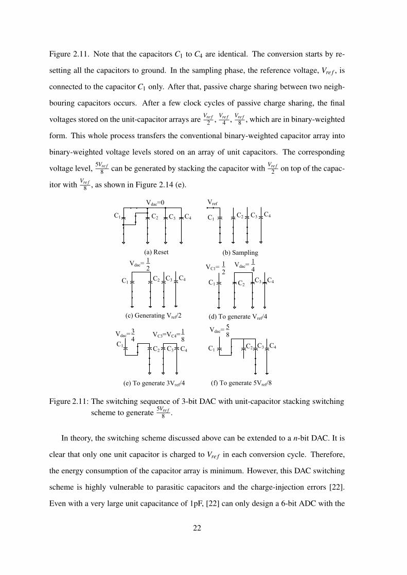
Figure 2.11. Note that the capacitors C1 to C4 are identical. The conversion starts by re-
setting all the capacitors to ground. In the sampling phase, the reference voltage, Vre f , is
connected to the capacitor C1 only. After that, passive charge sharing between two neigh-
bouring capacitors occurs. After a few clock cycles of passive charge sharing, the final
voltages stored on the unit-capacitor arrays are Vre f2 , Vre f
4 , Vre f8 , which are in binary-weighted
form. This whole process transfers the conventional binary-weighted capacitor array into
binary-weighted voltage levels stored on an array of unit capacitors. The corresponding
voltage level, 5Vre f8 can be generated by stacking the capacitor with Vre f
2 on top of the capac-
itor with Vre f8 , as shown in Figure 2.14 (e).
C4C3C2C1
(a) Reset
Vdac=0 Vref
C4C3C2C1
(b) Sampling
C4C3C2C1
(c) Generating Vref/2
1
2Vdac=
C4C3C2C1
(d) To generate Vref/4
1
4Vdac=VC1=
1
2
C4C3C2
C1
(e) To generate 3Vref/4
3
4Vdac= VC3=VC4=
1
8C4C3C2C1
(f) To generate 5Vref/8
5
8Vdac=
Figure 2.11: The switching sequence of 3-bit DAC with unit-capacitor stacking switchingscheme to generate 5Vre f
8 .
In theory, the switching scheme discussed above can be extended to a n-bit DAC. It is
clear that only one unit capacitor is charged to Vre f in each conversion cycle. Therefore,
the energy consumption of the capacitor array is minimum. However, this DAC switching
scheme is highly vulnerable to parasitic capacitors and the charge-injection errors [22].
Even with a very large unit capacitance of 1pF, [22] can only design a 6-bit ADC with the
22

unit-capacitor stacking switching scheme for simulation. Apart from the limited accuracy,
unit-capacitor stacking scheme requires very complex switching sequence. The SAR logic
is much complex compared to the case for binary-weighted capacitor arrays.
2.3.2 Unit-capacitor Parallel Charge-Sharing
The unit-capacitor parallel charge-sharing switching scheme proposed in [6] always
uses passive charge-sharing and the unit capacitors are not stacked. Unlike the serial DAC
circuit discussed in [12], the unit-capacitor parallel charge-sharing switching scheme stores
the previously generated voltages on some unit capacitors for later charge-sharing. Every
DAC output voltage level to be generated in the next clock cycle is the average of the present
DAC voltage level and some previously generated voltage level. A simplified schematic of
the unit-capacitor parallel charge-sharing SAR-ADC is shown in Figure 2.12.
C0 C0 C0 C0 C0...
VrefVin
Figure 2.12: The unit-capacitor parallel charge-sharing SAR-ADC structure.
The size of the capacitor array as a function of the DAC resolution is shown in Figure
2.13 along with the equation describing the number of capacitors that are shared during
each conversion cycle (CB) to resolve B. The CB for each conversion can be determined
recursively by starting at the LSB (B = 0) and observing that minimally two unit capacitors
are required to generate the last reference voltage [6].
The operation of the unit-capacitor parallel charge-sharing switching scheme is illus-
trated with a 5-bit DAC switching sequence shown in Figure 2.14. In this example, the
sampled input is assumed to be 0.85Vre f . For a 5-bit ADC conversion, the 5 necessary
23

−=
−=
=
=
=
−
−
=∑
)1(,2
)2,...,3(,2
1
)2(,4
)1,0(,2
1
1
0
0
0
nBC
nBC
BC
BC
C
n
B
i
i
B
Bits (N)Unit-capacitor parallel
charge sharingConventional
5 8 32
6 12 64
7 20 128
8 28 256
9 44 512
10 64 1024
Figure 2.13: The number of unit capacitors for 5-10 bit ADC and the equation to calculatethe number of unit capacitors shared resolving bit B.
Vref
0 10 0 0 1 1 1
(a)
1
21
2
1
2
1
2
1
2
1
2
1
2
1
2
(b)
VDAC=1
2
1
21
2
1
2
1
21
2
1
21 1
(c)
Vref
1
2
1
2
1
2
1
23
4
3
4
3
4
3
4
(d)
VDAC=3
4
1 11
2
1
23
4
3
4
3
4
3
4
(e)
VrefVDAC=
7
8
1
2
1
23
4
3
4
7
8
7
87
8
7
8
(f)
VDAC=
1
2
1
23
4
131
6
7
87
8
7
8
131
6
131
6
(g)
VDAC=
1
2
1
23
4
273
2
7
8
7
8
131
6
273
2
27
32
(h)
Figure 2.14: The switching sequence of an ideal 5-bit DAC with unit-capacitor parallelcharge-sharing switching scheme for Vin = 0.85Vre f .
DAC voltages for the conversion are Vre f2 , 3Vre f
4 , 7Vre f8 , 13Vre f
16 , and 27Vre f28 , respectively. It can
be seen from Figure 2.14 that the first DAC voltage Vre f2 can be generated by switching
all the unit capacitors for charge sharing. To generate 3Vre f4 , it has to charge 2 capacitors to
Vre f . Then the two capacitors are connected with another two capacitors for charge sharing.
This is the same for generating 7Vre f8 . Other DAC voltage levels can be easily produced by
passive charge sharing.
The unit-capacitor parallel charge-sharing switching scheme does not always need to
24

charge the unit capacitors to Vre f in the conversion process. It first charges half of the unit
capacitors to reference voltage in sampling phase. If the sampled input voltage is larger
than half of the reference voltage, several unit capacitors are charged to Vre f again. If the
sampled input voltage is less than Vre f2 , some of the unit capacitors have to discharge to
ground. If the sampled input voltage is even larger or smaller, some more unit capacitors
have to be charged to Vre f or discharged to ground, respectively. The unit-capacitor par-
allel charge-sharing switching scheme does not consume energy more efficient than the
unit-capacitor stacking scheme. This is because the unit-capacitor parallel charge-sharing
switching scheme still consumes a substantial amount of energy if the sampled input volt-
age is large. On top of that, some unit capacitors are discharged to ground if the sampled
input voltage is small, resulting some energy wasted.
2.4 Conventional CR SAR ADC Component Energy Model
The lower bound of the conventional SAR ADC power consumption has been well
studied [11,23–26]. In [11], the energy models were developed for high-speed architecture
by assuming the comparator model as a pre-amplifier with a latch. The analysis in [23–26]
took a better understand in the modern deep-submicron technologies. However, the com-
parator was assumed to be a simple one-stage latched comparator. In many recent designs,
two-stage dynamic latched comparators were adopted [27–29]. Compared to single-stage
dynamic comparator with the same resolution, two-stage dynamic comparator can work
at higher speed and with lower power consumption. Therefore, a new energy model for
the two-stage dynamic comparator is discussed in this section. In addition, the power con-
sumption of the switch buffer that has not been discussed in previous works is also included
in this derivation. In this section, a more complete energy model for the SAR ADC is de-
veloped. With the developed energy model, a comparison for the binary-weighted DAC
capacitor array switching schemes is performed.
25

2.4.1 Capacitive DACs
The SAR ADC determines digital output bit serially by binary-search. During each
bit-cycling, one capacitor from each DACs is switched and energy is consumed during the
switching. The amount of energy drawn from the reference voltage by the DAC capacitor
arrays is proportional to the size of the unit capacitor. Assuming that the input signals are
uniformly distributed, the power consumed by the DAC for one conversion is
Pavg conv =n
∑i=1
2n+1−2i (2i −1)
C0V 2re f fs (2.7)
where Vre f is the reference voltage, fs is the sampling frequency, n is the resolution, and C0
is the unit capacitor.
2.4.2 Two-stage Dynamic Comparator
The dynamic latched comparators are widely employed in SAR ADCs due to their high
power efficiency. Although a single-stage dynamic latched comparator has possibly the
lowest transistor count, the two-stage dynamic latched comparator is also fairly popular
[27] due to its faster speed. Figure 2.15 (a) and (b) shows the schematics of conventional
single-stage and two-stage dynamic comparators, respectively. Both comparators work in
reset phase and regeneration phase. When CLK is low, the comparators are reset. All the
nodes are precharged or discharged to their respective reset voltages. In regeneration phase,
the differential outputs discharge toward ground at different rates depending on the input
voltages. When the voltages at these nodes are low enough, the PMOS transistors in the
cross-coupled inverters will turn on. One of the outputs is pulled to ground and the other is
pushed back to VDD.
The power consumption of a single-stage dynamic comparator was well studied [23,
24]. The power consumption of two-stage comparator can be derived using similar ap-
proach. The detailed derivation of two-stage dynamic comparator power consumption can
26

M1 M2
M3 M4M5 M6
V+ V-
CLK
CLK CLK
M7
(a) (b)
CLK
CLK
Vinp Vinn
Vo_d1 Vo_d2
id1 id2
M1 M2
1st stage
2nd stage
Figure 2.15: (a) A typical single-stage dynamic comparator and (b) a two-stage dynamiccomparator.
be found in Appendix B. The total power of a two-stage dynamic comparator is given by
Ptwostagecomp = 2n fsV 2DD (Co1 +0.5Co2)
+2 fsVDDVe f fCo2
[n ln
VDD (Vin −Vthn)
2Ainv∣∣Vthp
∣∣Vre f+
n(n+1)2
ln2+n
](2.8)
It can be seen from (2.8) that the comparator dynamic power depends on the parasitic
capacitances of the first and second stage outputs, and it is proportional to the resolution
of the ADC. The dynamic power is also dependent on the voltage at the comparator input
terminals. Reducing the transistor size would reduce the output capacitance. Hence the
power consumption can be reduced. However, comparator offset is inversely proportional
to the transistor size. In addition, the input-referred thermal noise must be limited to half
of a LSB. As a results, careful design of the comparator is required.
2.4.3 SAR Logic
In a conventional n-bit SAR ADC, the SAR logic circuit usually consists of a n-bit shift
register and n bit-registers. In general, there are 2n DFFs. The block diagram of a typical
SAR logic circuit [30] is shown in Figure 2.16.
27

Q
QSET
CLR
D
Q
QSET
CLR
D
Q
QSET
CLR
D
Q
QSET
CLR
D
Q
QSET
CLR
D
Q
QSET
CLR
D
Q
QSET
CLR
D
Q
QSET
CLR
D
Clk
Comparator
output
resetMSB
LSB
shift register
bit-register
Figure 2.16: Block diagram of a typical SAR logic.
The DFF can be implemented with conventional static logic gates. In practical design,
the DFFs used in the shift register and bit register are slightly different to save area and
power. The DFFs in the shift register have only asynchronous reset whereas the DFFs
in bit-registers have both asynchronous set and reset. In addition, the DFFs in the shift
register are driven by a constant clock signal, while the DFFs in the bit-register are only
triggered once per conversion. This means the DFFs in shift registers and bit registers carry
different switching activities. Therefore, the power consumption of the shift register and bit
register has to be derived separately. In literature, this difference is always overlooked. [31]
ignored the switching activity and the power consumption was overestimated. [23] assumed
an average switching activity of 0.4 because one-fourth of the transistors in the DFF are
clocked, which is inaccurate.
Conventional DFF with asynchronous reset is comprised of 2 NAND gates, 5 inverters
(including the one to generate complementary clock signal), and 4 transmission gates [31],
as shown in Figure 2.17.
Φ
Φ
Φ
Φ
D
RESET
Q
Φ
Φ
Φ
RESET
Φ
1
2
Φ
Φ
3
4
5
6
7
8
910
11
Figure 2.17: The conventional static DFF with asynchronous reset.
28

For simplicity, one NAND gate or NOR gate can be approximated to two minimum
sized inverters, and one Transmission Gate (TG) is equivalent to one inverter. The switch-
ing activities of each logic gate are to be determined. For example, it is obviously that
inverter 5 has switching activity of 1. The TG 6-9 turn ON and OFF in every clock cycle.
However, the logic state for these transmission gates changes only once in every ADC con-
version cycle. The switching activity is only 1/n. The switching activities of all the logic
gates are summarized in Table 2.2.
Table 2.2: Switching activity of each logic gate in the static DFF with asynchronous reset
Component number in Figure 2.17 Logic Gate Switching Activity1 Inverter 1/n2 Inverter 1/n3 Inverter 1/n4 Inverter 1/n5 Inverter 16 TG 1/n7 TG 1/n8 TG 1/n9 TG 1/n
10 NAND 1/n11 NAND 1/n
The switching activity summary in Table 2.2 is for one DFF in one clock cycle. For an
n-bit ADC, there n DFFs and n clock cycles. Summing all the switching activity, the power
consumption of the shift register can be derived as
Pshi f t−reg = n fs (12+n)CinvV 2DD (2.9)
where Cinv is the output capacitance of a minimum sized inverter.
The DFF with asynchronous set and reset employed in the bit-register consists of 2
NAND gates, 2 NOR gates, 3 inverters , and 4 transmission gates, as shown in Figure 2.18.
The operation of the DFFs in the bit-register is explained as follows. The DFF is ini-
tially reset, which causes the NAND gate and inverter at the output of the DFF to change
29

Φ
Φ Φ
Φ
Φ
Φ
Φ
Φ
D
SET
SETRESET
RESET
Q
Φ
Φ
Figure 2.18: The conventional static DFF with asynchronous set and reset.
states. After that, the DFF is set to high, and the associate NOR gates toggle once. After
that, the DFF will only be triggered once in each ADC conversion. As shown in Figure
2.16, the comparator output is the input signal to all the DFFs in the bit-register. The DFF
is supposed to latch the comparator output. When the DFF is triggered, all the logic gate
will toggle if the comparator output is “0”, and will remain unchanged if the comparator
output is “1”. Hence, the switching activities of the logic gates in the bit-register depend
on the ADC input signal.
The power consumption of the bit-register can be derived as
Pbit−reg = ηn fs (24+n)CinvV 2DD (2.10)
where η is the probability for the comparator output to be “0”.
The SAR logic power consumption can be derived by combining (2.9) and (2.10).
PSAR Logic = Pshi f t−reg +Pbit−reg
= n fs [n+12+η (n+24)]CinvV 2DD (2.11)
2.4.4 Switch Buffer Parasitic Capacitance Power
The SAR ADC capacitor arrays are driven by two sets of switch buffers. These switch
buffers can be realized with simple inverters, as shown in Figure 2.19.
30
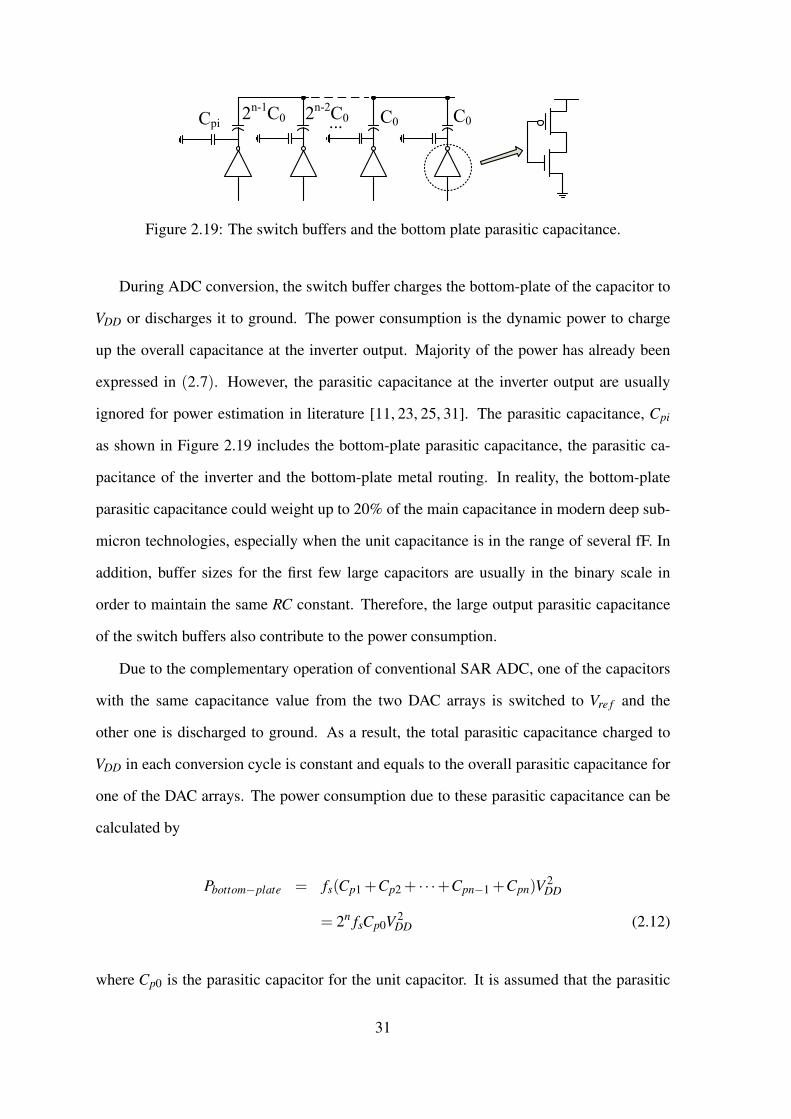
2n-1C0Cpi ...
2n-2C0 C0C0
Figure 2.19: The switch buffers and the bottom plate parasitic capacitance.
During ADC conversion, the switch buffer charges the bottom-plate of the capacitor to
VDD or discharges it to ground. The power consumption is the dynamic power to charge
up the overall capacitance at the inverter output. Majority of the power has already been
expressed in (2.7). However, the parasitic capacitance at the inverter output are usually
ignored for power estimation in literature [11, 23, 25, 31]. The parasitic capacitance, Cpi
as shown in Figure 2.19 includes the bottom-plate parasitic capacitance, the parasitic ca-
pacitance of the inverter and the bottom-plate metal routing. In reality, the bottom-plate
parasitic capacitance could weight up to 20% of the main capacitance in modern deep sub-
micron technologies, especially when the unit capacitance is in the range of several fF. In
addition, buffer sizes for the first few large capacitors are usually in the binary scale in
order to maintain the same RC constant. Therefore, the large output parasitic capacitance
of the switch buffers also contribute to the power consumption.
Due to the complementary operation of conventional SAR ADC, one of the capacitors
with the same capacitance value from the two DAC arrays is switched to Vre f and the
other one is discharged to ground. As a result, the total parasitic capacitance charged to
VDD in each conversion cycle is constant and equals to the overall parasitic capacitance for
one of the DAC arrays. The power consumption due to these parasitic capacitance can be
calculated by
Pbottom−plate = fs(Cp1 +Cp2 + · · ·+Cpn−1 +Cpn)V 2DD
= 2n fsCp0V 2DD (2.12)
where Cp0 is the parasitic capacitor for the unit capacitor. It is assumed that the parasitic
31

capacitance for each DAC capacitor is in binary-weighted form. The ratio of the bottom-
plate parasitic capacitance to the main capacitance of the unit capacitor can be defined as
β . Hence, (2.12) can be written as
PParasitic = 2n fsβC0V 2DD (2.13)
2.4.5 Composite Power
The total power consumption of conventional SAR ADC can be derived by summing
(2.7), (2.8), (2.11), & (2.13)
PSAR−ADC = fs
n
∑i=1
2n+1−2i (2i −1)
C0V 2re f +2n fsV 2
DD (Co1 +0.5Co2)
+2 fsVDDVe f fCo2
[n ln
VDD (Vin −Vthn)
2Ainv∣∣Vthp
∣∣Vre f+
n(n+1)2
ln2+n
]+n fs [n+12+η (n+24)]CinvV 2
DD +2n fsβC0V 2DD (2.14)
The importance of the equation (2.14) is that it gives the designer some basic under-
standing on the power breakdown of various SAR ADC components. Besides that, the
theoretical SAR ADC power consumption lower bound can also be obtained. For instance,
the DAC unit capacitor size can be determined by considering the capacitor mismatch.
Other parameters in (2.14) can be derived by assuming minimum size for the compo-
nents in a given technology. In addition, equation (2.14) also allows us to perform a
fair comparison on different DAC switching schemes. In literature, some DAC switch-
ing schemes [11, 18, 19] were adopted to reduce the DAC capacitor array switching power.
However, the comparison among various switching schemes was based on the DAC power
reduction only. The power and area overhead due to the complex switching schemes were
not discussed. With the derived equation (2.14), the overall ADC power consumption can
be derived for each switching scheme and a fair comparison can be done. Figure 2.20
shows an example of the conventional SAR ADC power versus resolution. Figure 2.21
shows the power breakdown of different components in a 10-bit SAR ADC. For both cases,
32

0 5 10 15 2010
−13
10−12
10−11
10−10
10−9
10−8
10−7
Resolution (bit)
Pow
er/f s (
J)
Figure 2.20: The theoretical power consumption of a conventional SAR ADC.
the following parameters are assumed: C0=10 fF, Co1=4 fF, Co2=5 fF, Ve f f =80 mV, VDD=1,
Cinv=10 fF, β = 5%,Vthn=0.45 V, Vthp=0.48 V, Ainv=10. It is observed from (2.14) that the
average power consumption is input-signal dependent. For simplicity, the input signal is
assumed to be uniformly distributed across the full scale input range and can be modeled
using η (Vin) = 0.7 [11]. It can be seen that the capacitor arrays consume majority of the
power. Therefore, switching schemes to reduce the capacitor arrays power are necessary.
26.72%
0.27% 0.74%
Cap array
SAR Logic
Bottom-plate parasitic
Comparator
72.27%
Comparator
Figure 2.21: The power breakdown of 10-bit SAR ADC.
33

2.4.6 Binary-weighted SAR ADC switching schemes theoretical energy comparison
With the derivation of SAR ADC theoretical power consumption, the previously dis-
cussed binary-weighted capacitor array SAR ADC switching schemes can be compared.
Figure 2.22 shows the comparison of average energy consumed in the DAC arrays ver-
sus ADC resolution. It can be seen that the power reduction of each switching scheme is
independent of the ADC resolution.
2 4 6 8 10 12 14 16 1810
−15
10−14
10−13
10−12
10−11
10−10
10−9
10−8
Resolution (bit)
Pow
er/f s (
J)
ConventionalCharge−recyclingSet−and−downVcm−based
Figure 2.22: The normalized power consumption of the capacitive DAC arrays at variousresolution.
However, some of the switching schemes introduce digital overhead. The simple switch-
ing energy comparison does not show the overall power or energy consumption of the
switching scheme. Therefore, the digital logic circuit power consumption should also
be considered for comparison. Benefited from the component energy model in equation
(2.14), the digital circuit energy or power consumption can be estimated for each switch-
ing scheme. Figure 2.23 shows the comparison of the normalized total power consumption
of ADCs with different switching schemes. It can be seen that ADCs with charge recycling
and set-and-down switching schemes do not necessarily have lower power consumption
compared to conventional one, at lower resolution. For more than 8-bit resolution, the
charge recycling and set-and-down switching schemes can save overall power consump-
tion of the ADCs. The Vcm-based switching scheme can always reduce power consumption
34

because it does not increase digital logic complexity. For all low-power switching schemes,
the power reduction capability is more or less fixed at higher resolution than 14-bit. This
means that the ADC power consumption is almost equal to the DAC capacitor array power
consumption as shown in Figure 2.22. The reason is that at higher resolution, the ADC
power consumption is completely dominant by the capacitive DAC arrays.
2 4 6 8 10 12 14 16 18
10−12
10−11
10−10
10−9
Resolution (bit)
Pow
er/f s (
J)
ConventionalCharge−recycleSet−and−downV
cm−based
Figure 2.23: The normalized total power consumption of ADCs with different switchingschemes at various resolution.
2.5 Summary
This chapter has discussed CR SAR ADC fundamentals and conventional switching al-
gorithm. The conventional switching scheme is energy inefficient for “down”-transitions.
Several low-power switching schemes, including the binary-weighted DAC capacitor array
and unit-capacitor array, are reviewed. A more comprehensive power consumption model
for the conventional SAR ADC is derived. With the new model, the binary-weighted DAC
capacitor array switching schemes are compared. It shows that some of the switching
schemes such as the charge-recycle switching scheme do not save ADC power at lower
resolution (≤ 8bit) because the digital overhead overweighes the power saving in the DAC
capacitor arrays. For the unit-capacitor DAC array switching schemes, the SAR logic is
generally very difficult for customization due to complex switching sequence. It is usually
35

implemented by Verilog-HDL. Since both unit-capacitor array and binary-weighted capac-
itor array switching schemes both have their own advantages and disadvantages, the author
will investigate both of them in this project. In the following chapter, a new unit-capacitor
array switching scheme is proposed.
36

Chapter 3
Ultra-Low Energy Unit-capacitor DAC
Array Switching Scheme for SAR ADC
This design serves as the first attempt in this project to explore the challenges in low-
to-medium speed low-power SAR implementation. An unit-capacitor voltage sampling
and charge-sharing switching scheme is proposed. This new switching scheme makes use
of the trade-off between speed and DAC switching power. By increasing the conversion
time, the proposed unit-capacitor array switching scheme uses multiple clock cycles to
generate the necessary reference voltage for conversion. Unlike the unit-capacitor parallel
charge-sharing [6], the proposed unit-capacitor switching scheme does not store any of the
previously generated voltage levels on capacitors. Instead, the proposed switching scheme
takes several intermediate clock cycles to generate the necessary voltage levels for charge-
sharing. As a result, less unit capacitors and switches are used in the proposed switching
scheme. An 8-bit design is simulated in Global Foundries 65nm CMOS process.
3.1 Unit-capacitor Voltage-sampling and Charge-sharing
Switching Scheme
A SAR-ADC using the proposed DAC switching scheme [29] [32] is shown in Figure
3.1. The proposed DAC array consists of n+1 unit capacitors and n+3 switches for n-
37

bit resolution. Initially, one unit capacitor is charged to the reference voltage, Vre f . In
subsequent conversion, charge redistribution occurs between 2 unit capacitors in each clock
cycle and the corresponding reference voltage levels, e.g. 12Vre f , 3
4Vre f , 14Vre f etc., are
then generated. A comparator compares the sampled input voltage and the generated DAC
reference voltages. Triggered by the output of the comparator, the SAR logic generates
control signals for all the switches to produce the correct reference voltage level for the
next bit decision. Similar switching methods are reported in [6] and [22].
Vref
…...
C0 C0 C0 C0
S1 S2 Sn Sn+1
S/HVin
SAROutput
Figure 3.1: The proposed SAR-ADC structure.
The operations of a 3-bit DAC using the proposed switching scheme are shown in Fig-
ure 3.2. The 3-bit DAC has 4 identical unit capacitors. The voltages sampled on each
capacitor at each clock cycle are also displayed in the figure. It can be seen that the pro-
posed switching scheme requires more clock cycles to generate a higher reference voltage
and less clock cycles for lower reference voltage. For example, it takes 6 clock cycles to
generate 78Vre f and 4 clock cycles for 1
8Vre f .
The number of extra clock cycles is different for each conversion. It needs to be worked
out case by case. For an 8-bit DAC with the proposed scheme, the maximum number
of clock cycles is 19 and the minimum number is 10. In a customized design, the SAR
logic must have one 19-bit shift-register so that the sampling rate of the 8-bit ADC is
synchronized to one clock frequency. The comparator must be disabled for those input
voltages that require less than 19 clock cycles for conversion. The simulated 8-bit DAC
38

Vref
Vref
b2=1
b2=0b1=1
b1=0
b1=1
b1=0
1 0
S1 S2 S3 S4
VDAC=Vref
1
2
1
2
0 0
S1 S2 S3 S4
VDAC=
1
2
1
2
Vref
2
Vref
1
S1 S2 S3 S4
VDAC=Vref
1
2
3
4
3
4
0
S1 S2 S3 S4
VDAC=
3
4
5
8
5
8
5Vref
8
S1 S2 S3 S4
VDAC=
1
2
3
4
7
8
7
8
7Vref
8
1
40
S1 S2 S3 S4
VDAC=
3
8
3
8
3Vref
8
S1 S2 S3 S4
VDAC=
1
2
1
4
1
8
1
8
Vref
8
1
40
S1 S2 S3 S4
VDAC=
1
2
1
4
Vref
4
1 0 0 0
S1 S2 S3 S4
VDAC=Vref
0 0 0 0
S1 S2 S3 S4
VDAC=00
S1 S2 S3 S4
VDAC=
1
2
3
4
3
4
3Vref
4
Figure 3.2: The complete switching sequence of a 3-bit DAC with the proposed switchingscheme.
voltage and comparator output waveforms for Vin = 0.28Vre f are shown in Figure 3.3. It
can be seen that 14 clock cycles are needed for this conversion.
Figure 3.3: The simulated comparator output and DAC output voltage waveforms.
3.2 Switching Energy Analysis
The proposed DAC switching scheme does not need to charge one capacitor to Vre f
in every clock cycle. It only charges the capacitors to reference voltage when necessary.
The complete 3-bit DAC switching sequence is shown in Figure 3.2. It can be seen that
39

the larger the input voltage is, the more capacitors need to be charged to Vre f during the
conversion. For instance, if the input voltage is larger than 34Vre f , three unit capacitors are
charged to Vre f . If the input voltage is less 12Vre f , only one unit capacitor is charged to Vre f .
The DAC switching energy for each bit conversion can be calculated by the following
equations. If the input voltage is less than 12Vre f , the switching energy is determined by
charging only one capacitor to reference voltage.
E1/2 =12
CV 2re f (3.1)
If the input voltage is between 12Vre f and 3
4Vre f , two capacitors are charged to Vre f . The
switching energy is given by:
E1/2−3/4 =12
CV 2re f ×2 =CV 2
re f (3.2)
If the input voltage level is larger than 34Vre f , three capacitors are charged to the refer-
ence voltage. The total switching energy can be expressed as:
E3/4 =12
CV 2re f ×3 =
32
CV 2re f (3.3)
The switching energies of the 3-bit DAC with the associated input voltage levels are sum-
marized in Table 3.1
Figure 3.4 shows the simulated switching energy comparison for the proposed switch-
ing scheme and the other two unit-capacitor DAC array switching schemes in literature. All
three ADCs are designed and simulated in the same 65nm CMOS process. All simulations
are conducted with ramp input signals and sampling rate of 100 kS/s. The simulated power
consumption for the proposed DAC is 110 nW at 1.0 V power supply.
40

Table 3.1: Input voltage and the corresponding switching energy consumption
Equivalent digital code ofinput voltage
Switching Energy
000 12CV 2
re f
001 12CV 2
re f
010 12CV 2
re f
011 12CV 2
re f
100 CV 2re f
101 CV 2re f
110 32CV 2
re f
111 32CV 2
re f
0 50 100 150 200 2500
0.5
1
1.5
2
2.5
3
3.5
4
4.5
5
Digital code
Sim
ulat
ed s
witc
hing
ene
rgy
(pJ)
Ref.[22]Ref.[6]The proposed
Figure 3.4: Simulated switching energy comparison of the three unit-capacitor arrayswitching schemes.
41
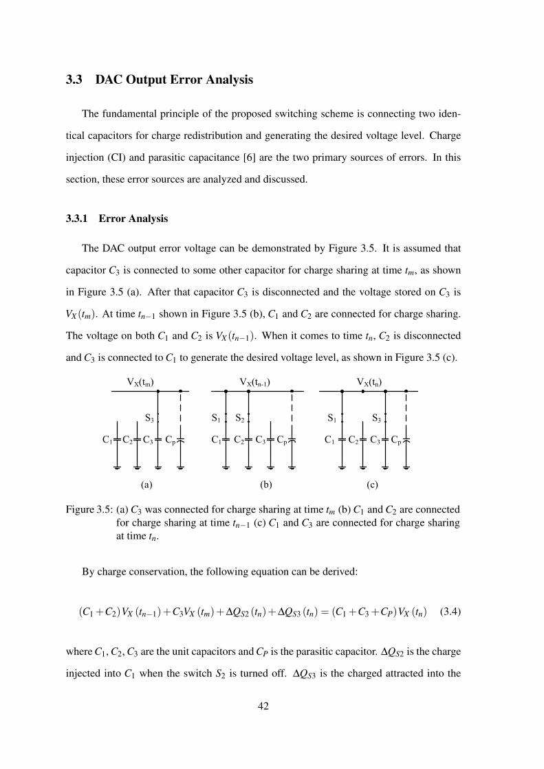
3.3 DAC Output Error Analysis
The fundamental principle of the proposed switching scheme is connecting two iden-
tical capacitors for charge redistribution and generating the desired voltage level. Charge
injection (CI) and parasitic capacitance [6] are the two primary sources of errors. In this
section, these error sources are analyzed and discussed.
3.3.1 Error Analysis
The DAC output error voltage can be demonstrated by Figure 3.5. It is assumed that
capacitor C3 is connected to some other capacitor for charge sharing at time tm, as shown
in Figure 3.5 (a). After that capacitor C3 is disconnected and the voltage stored on C3 is
VX(tm). At time tn−1 shown in Figure 3.5 (b), C1 and C2 are connected for charge sharing.
The voltage on both C1 and C2 is VX(tn−1). When it comes to time tn, C2 is disconnected
and C3 is connected to C1 to generate the desired voltage level, as shown in Figure 3.5 (c).
C1 C2 C3 Cp
VX(tn-1)
S1 S2
C1 C2 C3 Cp
VX(tn)
S1 S3
C1 C2 C3 Cp
VX(tm)
S3
(a) (b) (c)
Figure 3.5: (a) C3 was connected for charge sharing at time tm (b) C1 and C2 are connectedfor charge sharing at time tn−1 (c) C1 and C3 are connected for charge sharingat time tn.
By charge conservation, the following equation can be derived:
(C1 +C2)VX (tn−1)+C3VX (tm)+∆QS2 (tn)+∆QS3 (tn) = (C1 +C3 +CP)VX (tn) (3.4)
where C1, C2, C3 are the unit capacitors and CP is the parasitic capacitor. ∆QS2 is the charge
injected into C1 when the switch S2 is turned off. ∆QS3 is the charged attracted into the
42

channel of S3 when the switch S3 is turned on. VX(tn−1) and VX(tm) are the voltage levels
on capacitor C1 and C3 before time tn, respectively. VX(tn) is the voltage to be generated at
time tn. They all can be expressed by the sum of their ideal values and some error voltages.
VX (tm) = VX0 (tm)+ εX (tm) (3.5)
VX (tn−1) = VX0 (tn−1)+ εX (tn−1) (3.6)
VX (tn) = VX0 (tn)+ εX (tn) (3.7)
where VX0(tm), VX0(tn−1) and VX0(tn) are the desired DAC output voltage levels at time tm,
tn−1 and tn, respectively. εX(tm), εX(tn−1) and εX(tn) are the error voltages at time tn, tn−1
and tm, respectively.
Thus, the DAC output voltage at time tn can be derived from (3.4) (3.5) (3.6) and (3.7).
The ideal DAC output voltage at time tn is given by:
VX0 (tn) =VX0 (tn−1)+VX0 (tm)
2(3.8)
The error voltage on the DAC output at tn can be expressed:
εX (tn) =(C1 +CP)εX (tn−1)+C1εX (tm)
2C1 +CP+
CP2 (C1 +CP) [VX0 (tn−1)−VX0 (tm)]
2C1 +CP
+∆QS2 (tn)+∆QS3 (tn)
2C1 +CP(3.9)
It can be seen from (3.9) that the error voltage for a particular DAC voltage level de-
pends on the error voltages of the two voltage levels that are previously generated to pro-
duce the present DAC output voltage, the parasitic capacitance as well as charge injection
due to the two switches. Next, the charge injection errors caused by switches S2 and S3 are
investigated. Figure 3.6 shows the charge injection from switches S2 and S3.
The charge injection of analog switches in ADC designs has been extensively studied
in literature and complex modeling techniques were suggested [33–37]. Dummy switches
43

C1 C2 C3 Cp
VX(tn-1)
R1
S2
(a)
0 VDD
VDD 0
C1 C2 C3 Cp
VX(tn)
R1
S2
(b)
VDD 00 VDD
Figure 3.6: (a) Channel charges injected into C1 and C2 when S2 is turned off. (b) Chargesare attracted into the channel when S3 is turned on.
are implemented to cancel the charge-injection in S/H circuits [36]. However, the switches
in this design are implemented with minimum sized TG without any dummy switches. The
analytical justification of selecting switch configuration is discussed in Appendix C. With
the minimum sized TG switches, the amount of charge injection produced by these switches
depends on the biasing voltages of the switches [33, 34]. The biasing voltages, VX(tn−1)
and VX(tm), determine whether NMOS or PMOS is on. Figure 3.7 plots the NMOS and
PMOS conductance at different input voltages. Three conduction regions are identified in
the figure. In region A, only NMOS is on. In region C the PMOS is on. In region B, both
NMOS and PMOS are conducting. There are 8 possible combinations for ∆QS2 and ∆QS3.
All the equations to determine ∆QS2 and ∆QS3 for all eight combinations are summarized
in Appendix D, and the conditions are summarized in Table D.2.
An example of the charge injection error of ∆QS2 and ∆QS3 is shown below for both
NMOS and PMOS on, i.e. Vt p < VX(tn−1) < VDD −Vtn and VX(tm) > VX(tn−1). This case
is corresponding to the region B in figure 3.7.
∆QS2 (tn) =12
CoxpWpLp[VX (tn−1)−Vthp
]+CovpVDD
−12
CoxnWnLn [VDD −VX (tn−1)−Vthn]−CovnVDD (3.10)
∆QS3 (tn) = CoxnWnLn [VDD −VX (tn−1)−Vthn]
+2CovnVDD −CoxpWpLp[VX (tm)−Vthp
]−2CovpVDD (3.11)
44
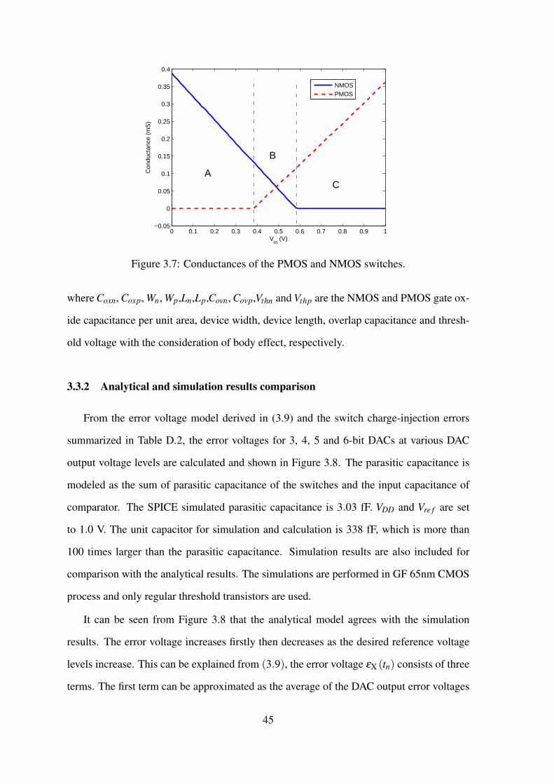
0 0.1 0.2 0.3 0.4 0.5 0.6 0.7 0.8 0.9 1−0.05
0
0.05
0.1
0.15
0.2
0.25
0.3
0.35
0.4
Vin
(V)
Con
duct
ance
(m
S)
NMOSPMOS
B
AC
Figure 3.7: Conductances of the PMOS and NMOS switches.
where Coxn, Coxp, Wn, Wp,Ln,Lp,Covn, Covp,Vthn and Vthp are the NMOS and PMOS gate ox-
ide capacitance per unit area, device width, device length, overlap capacitance and thresh-
old voltage with the consideration of body effect, respectively.
3.3.2 Analytical and simulation results comparison
From the error voltage model derived in (3.9) and the switch charge-injection errors
summarized in Table D.2, the error voltages for 3, 4, 5 and 6-bit DACs at various DAC
output voltage levels are calculated and shown in Figure 3.8. The parasitic capacitance is
modeled as the sum of parasitic capacitance of the switches and the input capacitance of
comparator. The SPICE simulated parasitic capacitance is 3.03 fF. VDD and Vre f are set
to 1.0 V. The unit capacitor for simulation and calculation is 338 fF, which is more than
100 times larger than the parasitic capacitance. Simulation results are also included for
comparison with the analytical results. The simulations are performed in GF 65nm CMOS
process and only regular threshold transistors are used.
It can be seen from Figure 3.8 that the analytical model agrees with the simulation
results. The error voltage increases firstly then decreases as the desired reference voltage
levels increase. This can be explained from (3.9), the error voltage εX (tn) consists of three
terms. The first term can be approximated as the average of the DAC output error voltages
45

0 0.2 0.4 0.6 0.8 10
1
2
3
4
Ver
r (m
V)
3−bit
calculationsimulation
0 0.2 0.4 0.6 0.8 10
1
2
34−bit
calculationsimulation
0 0.2 0.4 0.6 0.8 1−1
0
1
2
3
Vx(t
n)
Ver
r (m
V)
5−bit
calculationsimulation
0 0.2 0.4 0.6 0.8 1−1
0
1
2
3
Vx(t
n)
6−bit
calculationsimulation
Figure 3.8: Comparison between analytical model and spice simulation results for 3, 4, 5and 6-bit DAC.
at time tn−1 and tm, respectively. The second term is proportional to the difference of the
desired voltage levels at tn−1 and tm, respectively, and the last term is the sum of the charge-
injection errors due to switches S2 and S3. When the desired reference voltage level is very
large or very small, the two previously generated ideal voltage levels are close to each other.
Thus, the difference of these two ideal voltage levels is small. As a result, the second term
in (3.9) is also very small. Therefore the overall DAC output error voltage is small. When
the desired reference voltage level is close to the center of the reference voltage range, the
difference of the two ideal voltage levels is large. The resulting DAC error voltage is large.
This can be observed in Figure 3.8. The DAC output error voltage is smaller towards the
two ends of the reference voltage and is larger in the center. The second term in (3.9)
can also be positive or negative during the switching sequence depending on the desired
reference voltage level. As a result, the DAC output voltage plot is not a smooth curve but
running up and down as seen in Figure 3.8. The derived model can be used to calculate
the DAC output error voltage. However, there is no compact-form equation to predict the
maximum error voltage due to the nature of the proposed switching scheme. The maximum
46

deviation has to be determined via exhaustive analysis.
3.4 ADC Simulation Results and Comparisons
An 8-bit single-ended SAR ADC with the proposed unit-capacitor voltage sampling
and charge-sharing switching scheme was simulated in Global Foundries 65nm CMOS
process. The dynamic comparator was designed with rail-to-rail input signal swing [29].
The unit-capacitor parallel charge-sharing switching scheme [6] is also simulated in the
same platform for a fair comparison.
In Table 3.2, the simulated power consumption of the proposed ADC and Ref. [6] is
summarized. Both ADCs were simulated with the same dynamic comparator and unit
capacitance. The SAR logic for both ADCs was implemented with Verilog-HDL. It is clear
that the proposed unit-capacitor switching scheme has advantages in power consumption
over [6]. The unit-capacitor array switching scheme in [22] was not simulated and excluded
for simulation power comparison. The reason is that the switching scheme in [22] does not
guarantee 8-bit accuracy. In [22], a 6-bit design was reported with simulation results despite
large unit capacitors of 1pF were used.
Table 3.2: Comparison of simulated power consumption
Component The proposed Ref. [6]
Capacitor array 110 nW 330 nW
SAR logic 2.29 µW 4.05 µW
Comparator 400(avg.) nW 400 nW
Total 2.8 µW 4.75 µW
Table 3.3 compares the three switching schemes in terms of the number of capacitors,
the number of switches and the number of clock cycles. The proposed DAC scheme uses
only one third of the total capacitance as the DAC scheme in [6]. Compared with DAC
scheme in [22], the proposed scheme uses only 33% of analog switches as the scheme
in [22] does. It is clear that the proposed switching scheme has the smallest area at the
expenses of increased conversion time.
47

Table 3.3: Comparison of hardware and conversion time
DAC scheme No. of capacitors No. of switches No. of clock cycles
conv. 2n 2∗n n+1
[22] n+1 4n+1 n+3
[6] (8bit) 28 3∗28 16
Proposed (8bit) n+1 (9) n+3 (11) 19
ADCs are characterized by both static and dynamic parameters. Differential Non-
Linearity (DNL) and Integral Non-Linearity (INL) are the ADC main static parameters.
For an ideal ADC, the output is divided into 2n uniform steps and each step has width ∆.
Any deviation from the ideal step width is the Differential Non-Linearity. DNL errors ac-
cumulate to produce a total Integral Non-Linearity. The INL is defined as the maximum
deviation from the ideal slope of the ADC, which is measured from the centre of the step.
Figure 3.9 shows the simulated DNL and INL of the proposed ADC. The simulation
is performed with ramp input signal at 100 kS/s sampling rate. The DNL is within ±
0.4 LSB and INL is less than 1 LSB. The DNL and INL errors are based on transistor level
simulations, which does not involve any Monte Carlo models for the capacitors. Hence, the
DNL and INL errors are mainly caused by the charge-injection errors and does not reflect
the actual ADC linearity. With 0.4 LSB DNL error and 0.8 LSB INL error in simulation,
it is reasonable to believe that the actual ADC linearity should be much worse considering
the capacitor mismatch.
3.5 Summary
This chapter provides an insight to the various unit-capacitor switching schemes and
also proposes a new scheme that consumes lower energy. Detailed switch charge-injection
errors were derived, analyzed, and simulated. Although the proposed unit-capacitor volt-
age sampling and charge-sharing switching scheme shows ultra-low switching energy by
normalizing to CV 2re f in theory, it requires large unit capacitance (330fF) to achieve 8-bit
48

0 50 100 150 200 250−0.4
−0.2
0
0.2
0.4
Digital codesD
NL
(LS
B)
0 50 100 150 200 2500
0.2
0.4
0.6
0.8
1
Digital codes
INL
(LS
B)
Figure 3.9: Simulated INL and DNL of the proposed SAR-ADC.
resolution. In contrast, the binary-weighted DAC switching schemes utilize much smaller
unit capacitors, in the range of several fF. As a result, the DAC array of the proposed unit-
capacitor array switching scheme may consume more energy than the binary-weighted ca-
pacitor arrays. For example, the average switching energy of an 8-bit ADC with the set-and-
down switching scheme can be derived as 63.5CV 2re f while the average switching energy
of the proposed switching scheme is derived by 1.63CV 2re f . The ADC with set-and-down
switching scheme can be implemented with a unit capacitor size as low as 5fF [17] and
the average switching energy is about 0.32 pJ. The proposed unit-capacitor array switch-
ing scheme has average switching energy of 0.54 pJ. Therefore, the proposed switching
scheme consumes more energy because the unit capacitance is more than 60 times larger.
In addition, the SAR logic for the unit-capacitor switching scheme could be very com-
plex for customization due to the asymmetric switching sequence. The power consumption
of the SAR logic can easily overweight the power reduction in the DAC capacitor array.
Furthermore, the unit-capacitor array switching schemes cannot be easily implemented in
differential structure whereas the binary-weighted ADCs can be easily designed in differ-
ential structure. Hence, the author concludes that the unit-capacitor voltage sampling and
charge-sharing switching scheme is not a compatible switching scheme for biomedical ap-
49

plications despite its ultra-low switching energy in theory. Therefore, the binary-weighted
capacitor array SAR ADC is the ultimate candidate for biomedical applications due to its
low-power and ease of SoC integration.
50

Chapter 4
A 281nW 8-ENOB Asynchronous SAR
ADC Featuring Tri-Level Switching in
65nm CMOS
The previous chapter reported an initial study of the unit-capacitor DAC array switching
scheme as well as the DAC output error due to charge injection. Analysis showed that the
unit-capacitor switching scheme lost the advantage of ultra-low power characteristics due
to the digital circuit overhead as well as large unit capacitance. It seemed the unit-capacitor
switching scheme was not suitable for biomedical applications, but could probably find
its application in MCU-based systems. The design was not fabricated, and the research
direction was moved to investigation of the binary-weighted capacitive DAC switching
schemes.
In this chapter, a 281nW 8-ENOB asynchronous SAR ADC operating at 25 kS/s that
was fabricated in 65nm CMOS process is presented. The ADC employs a novel low-energy
and area-efficient tri-level switching scheme in the DAC. Compared to the conventional
SAR ADC, the average switching energy and total capacitance are reduced by 97% and
75%, respectively. A delay-based internal clock generator produces a high-speed signal
that allows True Single Phase Clock (TSPC) DFF to be used in the low-speed biomedical
applications. The leakage current is minimized in system level by combining the sampling
51

phase with the resetting phase. The prototype ADC achieves the best performance at 25
kS/s with 50.1 dB SNDR and 55.3 dB SFDR operating at 1 V supply. The ADC consumes
281 nW and exhibits a FoM of 43.3 fJ/conversion-step.
4.1 ADC Architecture
The architecture of the proposed ADC is shown in Figure 4.1. A differential structure is
employed to have good common-mode noise rejection. The proposed SAR ADC consists
of two binary-weighted capacitor arrays, two bootstrapped switches, a dynamic compara-
tor, a delay-based internal clock generator, SAR logic controller and digital output logic
circuits. Unlike the conventional SAR ADC architecture that has 2n unit capacitors in each
capacitor array for n-bit design, the proposed ADC uses only 2n−2 in each DAC capacitor
array, which results in 75% reduction in DAC capacitor array area. The proposed SAR
ADC uses top-plate sampling technique by sampling the input differential voltages on the
top-plate of the capacitor arrays, which has been seen in many low-power SAR ADCs in
literature [17, 20, 38].
Delay-based Internal
clock generator
SAR Control Logics
Vref
Vref
Vcm
Vcm
EOCValid
…...
D0 D1 D8 D9
Sampling clock,
Clks
Comp_clk
DOL (Digital Output Logic)
…...
MUX
Von
Vop
Result
GND
GND
VINP
VINN
C0UC1UC7U
C8U
C8L C7L C1L C0L
Bootstrapped
MSB
Figure 4.1: Architecture of the proposed ADC.
Asynchronous timing control is used in the proposed ADC to avoid using high-frequency
52

clock signal. Figure 4.2 shows the simplified timing diagrams for conventional SAR ADC
and the proposed SAR ADC, respectively. A conventional n-bit SAR ADC takes n clock
cycles for conversion and one or several clock cycles for sampling, as seen in Figure 4.2 (a).
In general, the clock frequency is at least n times faster than the sampling rate. The con-
ventional timing scheme is not an optimized approach from the power consumption point
of view. In case of a high-speed design, the sampling frequency is in the range of several
tens of MHz, and the required ADC clock is easily several hundreds of MHz. This high fre-
quency clock signal must be generated by some high-frequency clock generation circuitry,
which consumes large amount of power in addition to the ADC power consumption. For
low-to-medium speed design, which is within our target application, the clock period is
relatively long, in the range of tens of microsecond to millisecond. The time between one
switching activity to the next switching activity is so long that the leakage current could
generate significant errors at the DAC output. On top of that, the leakage current itself is
also large because the digital circuit internal nodes are in transition throughout the entire
conversion period. For example, the leakage power for the SAR ADC running at 1 kS/s
in [39] is about 25% of the overall power consumption.
The proposed ADC is running at a low system clock signal that is at the same frequency
as the sampling rate, as shown in Figure 4.2 (b). The ADC samples the input signals and
resets the digital circuit when the system clock is high. The conversion starts when the
system clock goes low. An internal high frequency signal that drives the comparator is
generated at the falling edge of the system clock by an internal clock generator circuit.
Then the differential output signals of the comparator produce the Valid signal that clocks
the SAR logic. The frequency of the internal clock signal is mainly controlled by the
delay element in the internal clock generator. In this way, the high frequency internal
signal eliminates the leakage current induced error on the DAC capacitor arrays. More
importantly, the digital circuit is in reset phase after the conversion phase. Hence, the
leakage current can be minimized.
53

Master_clk
Comp_clk
Vop
EOC
ADC output
Valid
Von
Conversion Sampling &
Reset
ConversionSample
Conversion
(a)
(b)
Master_clk
Figure 4.2: (a)The timing diagram of conventional SAR ADC and (b) The timing diagramof the proposed ADC.
4.2 Novel Tri-Level Switching Scheme
The SAR logic circuit controls the switches according to the proposed tri-level switch-
ing scheme [40, 41]. The proposed tri-level switching scheme makes use of the input
common-mode voltage Vcm as the third voltage level for conversion, besides Vre f and
ground. However, the input common-mode voltage Vcm is directly used for the 2nd-MSB
conversion in the proposed switching scheme by passive charge-redistribution. As a result,
no energy is consumed in the second bit conversion, unlike in the Vcm-based conversion
in [20]. In addition, the total capacitance is also reduced by half compared to the Vcm-based
switching. Furthermore, the proposed tri-level switching scheme only activates one of the
capacitor arrays for switching while resetting the other. This single-sided switching tech-
nique allows only one of the capacitor arrays to actively switch to either Vre f or ground. As
a result, more energy saving is achieved compared to Vcm-based switching which switches
both DAC capacitor arrays during conversion. Figure 4.3 shows a 3-bit example of DAC
54

switching sequences for the Vcm-based and the proposed switching schemes.
CC2C
CC2C
Vip
Vin
CC2C
CC2C
0Vip – Vin >0?
0.5CVref2
0.5CVref2
Vip – Vin>Vref/2?
0.125CVref2
0.625CVref2
0.625CVref2
0.125CVref2
Vip – Vin >-
Vref/2?
Vcm
Vip – Vin >0?
0
Vip – Vin>0.5Vref?
Vip – Vin >
-0.5Vref?
Vip – Vin>0.75Vref?
Vip – Vin>0.25Vref?
Vip – Vin >
-0.25Vref?
Vip – Vin >
-0.75Vref?
0.125CVref2
Vip – Vin>0.75Vref?
Vip – Vin>0.25Vref?
Vip – Vin >
-0.25Vref?
Vip – Vin >
-0.75Vref?
CC2C
CC2C
Vcm
Vref
CC2C
CC2C
Vcm
VcmVref
CC
CC
CC
CC
Vcm
CC
CC
Vcm 0.125CVref2
0.125CVref2
0.125CVref2
CC
CC
Vip
Vin0
0
(a)
(b)
Vcm
Vcm
Vcm
Vcm
CC2C
CC2C
Vcm
Vcm
Vref
CC2C
CC2C
Vcm
VcmVrefVref
CC2C
CC2C
Vcm
VcmVref
CC2C
CC2C
Vcm
Vcm
Vref
Vref
CC
CC
VcmVref
CC
CC
Vcm
CC
CC
Vcm
VrefCC
CC
Vcm
Figure 4.3: (a) The switching sequence of the Vcm-based switching and (b) The proposedswitching scheme.
It can be observed from Figure 4.3 that the proposed switching scheme only switches
the DAC array that samples the lower input signal. The other side of the DAC array that
samples the higher input voltage is in idling mode. When the conversion finishes, the two
DAC capacitor arrays have the same voltage level. Figure 4.4 shows a comparison in the
DAC output waveforms for the Vcm-based switching scheme and the proposed switching
scheme. It can be concluded that the common-mode voltage of the reference DAC for the
55

proposed switching scheme does not converge to a fixed value at the end of the conversion.
The final common-mode voltage of differential DAC output depends on the sampled input
voltage. It can range from half Vre f to Vre f .
Vip
Vin
Sample 1 2 3 4 5
(b)
Vip
Vin
Sample 1 2 3 4 5
(a)
Figure 4.4: (a) DAC output waveforms of the Vcm-based switching and (b) the DAC outputwaveforms of the proposed switching scheme.
There are two other tri-level switching schemes [42, 43] published in literature. The
main difference between these two tri-level switching schemes and the proposed tri-level
switching scheme discussed in this section is the switching of capacitors from both sides
of the capacitor arrays in these two methods and the single-sided switching nature of the
proposed switching scheme. Another difference is the generation of the third reference
voltage. In the tri-level switching schemes discussed in [42, 43], the third voltage Vcm is
generated through passive charging sharing. When two identical capacitors that samples
two complementary voltages, Vinp and Vinn respectively, are connected for passive charge
sharing, the middle voltage in between of the two capacitors will be the average of Vinp
and Vinn, Vcm. The tri-level switching scheme in [42] is basically the Vcm-based switching
scheme with Vcm generated by passive charge-sharing. For the proposed tri-level switching
scheme as well as the Vcm-based switching scheme in [20], the third voltage level Vcm is
supplied from an external voltage.
Figure 4.5 shows the differential DAC output waveforms for all the three different tri-
level switching schemes. The first one in [42] is just like the Vcm-based switching, which
is symmetrical for the DAC arrays. For the asymmetric tri-level in [43], it is the same
as the first tri-level switching scheme except for the last bit conversion. For the last bit
56

conversion, the DAC which has higher output value remains unchanged. The other side of
the DAC array output will increase by 2 LSB so that the differential output is within 1 LSB.
For the proposed tri-level switching scheme, it is completely asymmetric. Only one side of
the DAC array is switched. From the ADC accuracy point of view, the asymmetric tri-level
in [43] is the best. However, the switching scheme is more complex than the proposed tri-
level. The digital circuit overhead will be much larger than the proposed switching scheme.
Vdacp
Vdacn
bit1 bit2 bit3
(a) (b) (c)
Only the LSB is
asymmetric switching
Tri-level in [42] Asymmetric tri-level in [43] The proposed tri-level
Figure 4.5: Comparison of the differential DAC output waveforms for three different tri-level switching schemes.
4.2.1 Linearity Analysis
The capacitors in SAR ADC capacitor arrays suffer from process variation. The capac-
itor mismatch limits the ADC linearity performance [18]. In this section, the worse-case
linearity performance of the proposed switching scheme is analyzed following the method
discussed in [44]. Each of the capacitors is modeled as the sum of the nominal capacitance
value and some error term:
Cn = 2n−1C0 +δn (4.1)
Ci = 2i−1C0 +δi (4.2)
57

where i is an integer representing the bit position, C0 is the unit capacitance and δi is the
error term. Assuming that the error distributions of the unit capacitors are independent and
are identically distributed Gaussian random variables. Then the error terms δn and δi are
independent. They have zero mean and the variances are given by
E[δ 2
0]= E
[δ 2
1]= δ 2
0 (4.3)
E[δ 2
n]= 2n−1δ 2
0 (4.4)
The linearity of SAR ADC is determined by the accuracy of the DAC outputs, which
are calculated for the case of no initial charge on the capacitor array (Vin = 0). For a given
DAC digital input value for the proposed switching scheme, y = ∑ni=1(Sn2n−1), where Si
represents the ADC decision for the i-th bit, the final voltage difference between two DAC
capacitor arrays must be considered for the following two cases: y ≥ 2n−1 and y < 2n−1.
The reason is that different capacitor array will be switched for these two cases. The voltage
difference of the two DAC is hence given by:
VDAC (y) =
Sn−2Cn−2+···+S1C1
∑n−2i=1 Ci
Vre f y ≥ 2n−1
(1−Sn−2)Cn−2+···+(1−S1)C1
∑n−2i=1 Ci
Vre f y < 2n−1
=
∑n−2
k=1 (2k−1C0+δk)Sk
2n−2C0+∑n−2i=1 δi
Vre f y ≥ 2n−1
∑n−2k=1 (2k−1C0+δk)(1−Sk)
2n−2C0+∑n−2i=1 δi
Vre f y < 2n−1
(4.5)
where Vre f is the reference voltage. The second term in the denominator of (4.5), ∆C =
∑n−2i=1 δi, will be neglected for this first cut analysis. Subtracting the nominal value yields
the error term shown in (4.6)
Verror (y)≈
∑n−2
k=1 δkSk2n−2C0
Vre f y ≥ 2n−1
∑n−2k=1 δk(1−Sk)
2n−2C0Vre f y < 2n−1
(4.6)
58

Hence, the variance of the error voltage is given by:
E[V 2
error (y)]
=
E[
∑n−2k=1 δ 2
k Sk
22n−4C20
V 2re f
]y ≥ 2n−1
E[
∑n−2k=1 δ 2
k (1−Sk)
22n−4C20
V 2re f
]y < 2n−1
=
∑n−2
k=1 2k−1Sk22n−4 ·
(σ0C0
)2·V 2
re f y ≥ 2n−1
∑n−2k=1 2k−1(1−Sk)
22n−4 ·(
σ0C0
)2·V 2
re f y < 2n−1
(4.7)
It can be seen from (4.7) that the variance for the two DAC input ranges(y ≥ 2n−1,y < 2n−1)
are identical. Hence, the maximum INL occurs at Vre f4 and 3Vre f
4 and the maximum INL val-
ues at these two input nodes are the same. The maximum INL error can be derived as:
(σINL)max = σINL
(FS4
−1)= σINL
(3FS
4−1)
=√
E [V 2error (2n−2 −1)] =
√2n−3 −122(n−2)
V 2re f ·
(σ0
C0
)2
≈√
2n+1 ·(
σ0
C0
)LSB (4.8)
The DNL of the capacitive DAC is the difference between the voltage errors across two
consecutive DAC outputs,
DNL(y) = ∆Verror (y) =Verror (y)−Verror (y−1) (4.9)
The maximum DNL also occurs at Vre f4 and 3Vre f
4 . Hence,
E[V 2
error(2n−2)−V 2
error(2n−2 −1
)]= E
(δn−2 −∑n−3k=1 δk
2n−2C0Vre f
)2=
σ20
22n−4C20
V 2re f (4.10)
Therefore, the maximum DNL is given by
σDNL,max = 2√
2n
(σ0
C0
)LSB (4.11)
59

A comparison between the proposed tri-level switching scheme and other switching
schemes is necessary. Behavioral simulations of the SAR ADC for 1000 Monte Carlo runs,
with different switching schemes are performed. The unit capacitors are assumed to be
Gaussian random variables with standard deviation of 3% (σ/C0 = 0.03) [11, 45].
0 500 10000
0.35
0.7
σ DN
L (
LSB
)
Conventional
0 500 10000
0.35
0.7Set−and−down
0 500 10000
0.35
0.7
Vcm
−based
0 500 10000
0.35
0.7Tri−level
0 500 10000
0.25
0.5
σ INL (
LSB
)
code0 500 1000
0
0.25
0.5
code0 500 1000
0
0.25
0.5
code0 500 1000
0
0.25
0.5
code
Figure 4.6: Behavioral simulation comparing the linearity of different switching schemes.
Figure 4.6 compares the standard deviation of linearity errors for different switching
schemes under the same operating conditions. It can be seen that the conventional SAR
ADC switching scheme has a larger peak DNL error and a smaller peak INL error than
the rest of the ADC switching schemes. The proposed SAR ADC is shown to have similar
linearity performance compared to the set-and-down and Vcm-based SAR ADCs since they
all have the same range of peak DNL and INL standard deviations. It is also noted that
there is some discrepancies between the analytical formula and simulation results for the
maximum standard deviations of DNL and INL. For example, the (σDNL)max and (σINL)max
calculated with (4.8) and (4.11) are 1.92 LSB and 1.36 LSB, while the maximum error val-
ues from Figure 4.6 are about 0.45 LSB and 0.47 LSB, respectively. The reason is because
60

the error term ∑n−2i=1 δi was omitted in the denominator when calculating the DNL and INL
standard deviations, making the calculated values larger than the simulation results.
4.2.2 Comparator Offset Effect
The main difference between the proposed SAR ADC and others is that the common-
mode voltage of the reference DAC changes with sampled input voltage levels. Since
comparator offset voltage is a function of the input voltage levels, the changing in the
comparator offset voltage will have some impact on the proposed SAR ADC performance.
For simple analysis, the comparator offset voltage is modeled as a first-order equation with
input voltage [17]:
Vos = ∆VT H1,2 +(VGS −VT H)1,2
2
(∆S1,2
S1,2+
∆RR
)(4.12)
where ∆VT H1,2 is the mismatch in threshold voltages of the input differential pair tran-
sistors, (VGS −VT H)1,2 is the overdrive voltage of the differential pair, ∆S1,2/S1,2 is the
physical dimension mismatch between the differential pair, and ∆R/R is the loading resis-
tance mismatch induced by load transistors. It can be seen that the offset voltage consists
of a constant term that does not affect ADC performance, and a voltage-dependent term.
The DNL of an ADC is a measure of the deviation of adjacent levels on the ADC
transfer curve from an ideal change of 1 LSB. It can be expressed as
DNL =∆Vactual
∆Videal−1 (4.13)
where ∆Vactual is the actual voltage change between adjacent codes and ∆Videal is the ideal
change. Within one conversion phase of SAR ADC, there is only one clock cycle in which
the comparator input signal is less than 1 LSB. The comparator offset voltage should be
considered only for this clock cycle. For the remaining clock cycles, the comparator does
not affect the decision because the input voltages are far apart. The actual voltage change
61
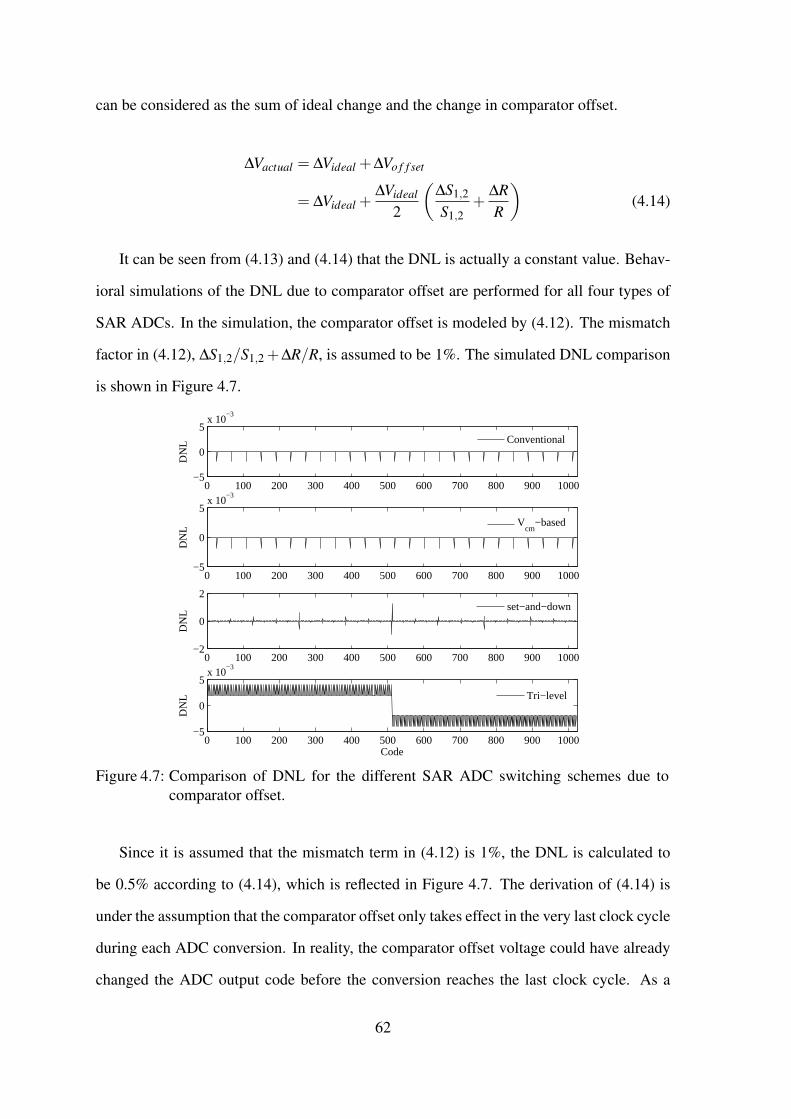
can be considered as the sum of ideal change and the change in comparator offset.
∆Vactual = ∆Videal +∆Vo f f set
= ∆Videal +∆Videal
2
(∆S1,2
S1,2+
∆RR
)(4.14)
It can be seen from (4.13) and (4.14) that the DNL is actually a constant value. Behav-
ioral simulations of the DNL due to comparator offset are performed for all four types of
SAR ADCs. In the simulation, the comparator offset is modeled by (4.12). The mismatch
factor in (4.12), ∆S1,2/S1,2 +∆R/R, is assumed to be 1%. The simulated DNL comparison
is shown in Figure 4.7.
0 100 200 300 400 500 600 700 800 900 1000−5
0
5x 10
−3
DN
L
Code
0 100 200 300 400 500 600 700 800 900 1000−5
0
5x 10
−3
DN
L
Conventional
0 100 200 300 400 500 600 700 800 900 1000−5
0
5x 10
−3
DN
L
V
cm−based
Tri−level
0 100 200 300 400 500 600 700 800 900 1000−2
0
2
DN
L
set−and−down
Figure 4.7: Comparison of DNL for the different SAR ADC switching schemes due tocomparator offset.
Since it is assumed that the mismatch term in (4.12) is 1%, the DNL is calculated to
be 0.5% according to (4.14), which is reflected in Figure 4.7. The derivation of (4.14) is
under the assumption that the comparator offset only takes effect in the very last clock cycle
during each ADC conversion. In reality, the comparator offset voltage could have already
changed the ADC output code before the conversion reaches the last clock cycle. As a
62
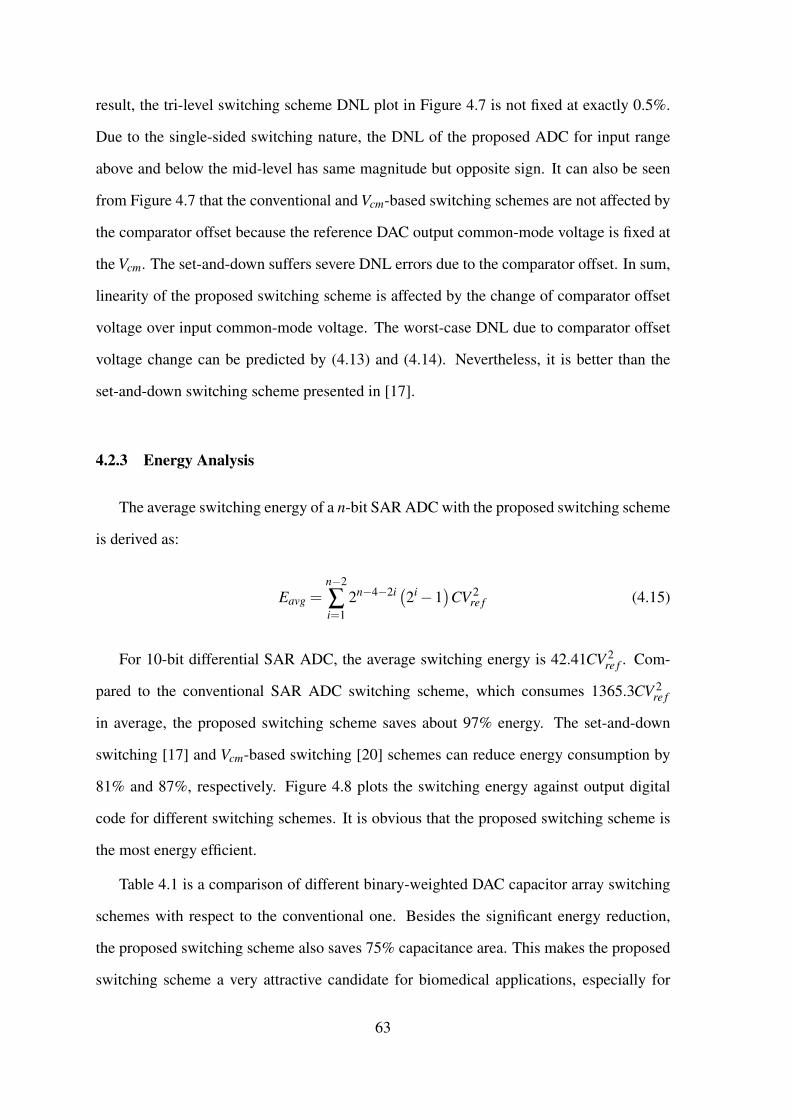
result, the tri-level switching scheme DNL plot in Figure 4.7 is not fixed at exactly 0.5%.
Due to the single-sided switching nature, the DNL of the proposed ADC for input range
above and below the mid-level has same magnitude but opposite sign. It can also be seen
from Figure 4.7 that the conventional and Vcm-based switching schemes are not affected by
the comparator offset because the reference DAC output common-mode voltage is fixed at
the Vcm. The set-and-down suffers severe DNL errors due to the comparator offset. In sum,
linearity of the proposed switching scheme is affected by the change of comparator offset
voltage over input common-mode voltage. The worst-case DNL due to comparator offset
voltage change can be predicted by (4.13) and (4.14). Nevertheless, it is better than the
set-and-down switching scheme presented in [17].
4.2.3 Energy Analysis
The average switching energy of a n-bit SAR ADC with the proposed switching scheme
is derived as:
Eavg =n−2
∑i=1
2n−4−2i (2i −1)
CV 2re f (4.15)
For 10-bit differential SAR ADC, the average switching energy is 42.41CV 2re f . Com-
pared to the conventional SAR ADC switching scheme, which consumes 1365.3CV 2re f
in average, the proposed switching scheme saves about 97% energy. The set-and-down
switching [17] and Vcm-based switching [20] schemes can reduce energy consumption by
81% and 87%, respectively. Figure 4.8 plots the switching energy against output digital
code for different switching schemes. It is obvious that the proposed switching scheme is
the most energy efficient.
Table 4.1 is a comparison of different binary-weighted DAC capacitor array switching
schemes with respect to the conventional one. Besides the significant energy reduction,
the proposed switching scheme also saves 75% capacitance area. This makes the proposed
switching scheme a very attractive candidate for biomedical applications, especially for
63

0 200 400 600 800 10000
200
400
600
800
1000
1200
1400
1600
1800
Digital code
Sw
itchi
ng E
nerg
y (C
Vre
f2
)
ConventionalCharge−recycleSet−and−downV
cm−based
Proposed
Figure 4.8: Switching energy comparison.
some bio-implantable systems. The SAR logic for the proposed switching scheme can be
implemented in different ways depending on the switch network design. In the present
prototype, three sets of DFFs are required, just like the set-and-down switching schemes
[17]. This inevitably increases the digital circuit power consumption and area compared
to conventional SAR ADC logic circuit. In order to overcome the digital circuit overhead
and maintain the power saving capability of the proposed switching scheme, the proposed
ADC employs TSPC dynamic DFFs instead of conventional static DFFs.
Table 4.1: Comparison of different switching schemes for 10-bit cases
Switching energySchemes
(CV 2re f )
Energy saving Area saving No. of DFFs
Conventional [13] 1363.33 Ref. Ref. 2n
Charge-recycle [18] 852.34 37.48% 0% 3(n−1)
Set-and-down [17] 255.5 81.26% 50% 3n
Vcm-based [20] 170.16 87.52% 50% 2n
Proposed [40] 42.41 96.89% 75% 3n
With the SAR ADC power consumption model derived in Chapter 2, theoretical power
64

4 6 8 10 12 14 1610
−12
10−11
10−10
10−9
Resolution (bit)
Pow
er/f s (
J)
conventionalcharge−recycleSet−and−downV
cm−based
Tri−level+conv DFFTri−level+TSPC DFF
Figure 4.9: Power consumption comparison for the SAR ADCs with differential binary-weighted switching schemes.
consumption comparison for the SAR ADCs with differential binary-weighted DAC array
switching schemes is shown in Figure 4.9. For the tri-level SAR ADC, derivations with
conventional DFFs and TSPC dynamic DFFs are included. It can be seen that the tri-
level switching scheme with conventional DFFs increases ADC power consumption at low
resolution. At resolution higher than 7-bit, the tri-level switching ADC with conventional
DFFs has lower power consumption than ADCs with the conventional, charge-recycle and
the set-and-down switching schemes. The tri-level switching ADC with conventional DFFs
has lower power than the Vcm-based switching scheme ADC for 12-bit or higher resolution.
With the TSPC dynamic DFFs, the proposed ADC has the lowest power consumption for
all resolution.
4.3 Circuit Implementation
In this section, the building blocks of the SAR ADC including binary-weighted capaci-
tor arrays, the dynamic comparator, the internal clock generator, the SAR logic circuit, are
discussed in details.
65

4.3.1 Capacitor Array
The proposed ADC consists of two binary-weighted DAC capacitor arrays. Each of
the capacitive DAC has 2n−2 unit capacitors. In order to minimize power consumption,
many designs [17, 27, 46, 47] uses unit capacitance in the range of fF. In [46], 8-bit SAR
ADC was designed with 0.5 fF unit capacitance. [47] even managed to customize the unit
capacitance to 250aF where the capacitor array is segmented into 4-bit thermometer-coded
and 8-bit binary-coded. The maximum standard deviation of the DNL and INL of the
proposed ADC are derived in the previous section. It is clear that the DNL error has larger
standard deviation than the INL error according to (4.11) and (4.8) . Hence, only the σDNL
needs to be considered. The accuracy requirement on the unit capacitor for the proposed
SAR ADC is set by the maximum allowable error:
3σDNL <12
LSB (4.16)
Combining (4.11) and (4.16) yields the matching requirement on the unit capacitor for
the proposed 10-bit SAR ADC: (σ0
C0
)< 0.26% (4.17)
In the 65nm process used, two closely placed asymmetrical Metal-Oxide-Metal (MOM)
capacitors with 10 fF capacitance each would have about 0.2% mismatch. By considering
the power and accuracy constraints, a 10 fF MOM unit capacitor whose dimensions are
2.7 µm × 2.9 µm is chosen. That would give rise to a 2.56 pF input capacitance for each
capacitor array. Common-centroid layout technique is adopted for better matching
4.3.2 Low Kickback Noise Dynamic Comparator
The comparator is crucial for the overall ADC power consumption. As shown in Figure
4.11, a two-stage dynamic comparator is used in this design. Since this design has no static
biasing, the average power consumption scales proportionally to the sampling frequency.
66

The first stage is a NMOS differential pair to amplify the small difference in the input
voltages. Since the common-mode voltage of the DAC capacitor array voltage is always in
the range of Vre f2 to Vre f , the NMOS differential pair is selected. The second stage is a pair
of cross-coupled inverters to form positive feedback.
Clk
ClkbClkb
Clk
Clk
Clk Clk
Vin+ Vin-
Vo+Vo-
Va Vb
Vc Vd
M3 M4
M1 M21st Stage
2nd Stage
Figure 4.10: The low-kickback noise dynamic comparator.
The operation of the dynamic comparator is well understood. The comparator is reset
when Clk is low and the outputs Vo+ and Vo− are reset to low. The regeneration phase
starts when Clk changes from low to high. The positive feedback in the cross-coupled
inverters resolves the output. When the latch circuits regenerate the differential signals,
the large voltage swings at the drains of the input transistors are coupled to the inputs
of the comparators through the parasitic capacitance, Cgd [48]. Since the sources to the
comparator have non-zero impedance, the input voltage of the comparator is disturbed.
This disturbance is referred as kickback noise and may cause the comparator to produce
erroneous results. The PMOS transistors M3 and M4 are introduced to reduce the voltage
swing at the drains of input differential pair. The voltage levels at Va and Vb are pulled
to VDD −Vthp at the beginning of regeneration phase to ensure that M3 and M4 stay in the
67

saturation region. Therefore, the voltage swing is reduced by a threshold voltage of the
PMOS, and hence the kickback noise is reduced.
Vd2
Vd1
Vb
Va
Figure 4.11: The voltage waveforms at the various nodes of the differential pair in regen-eration phase.
Since the DAC output common-mode voltage is not a fixed value, the comparator offset
will vary with the input voltage and degrade the ADC performance. In addition, it is also
impossible to calibrate the comparator offset for the same reason. Therefore, it is manda-
tory to keep the offset voltage as low as possible. Post-layout monte carlo simulations of
the comparator for input of 0.7 V shows an offset voltage with zero mean and 9 mV stan-
dard deviation. Considering a 3σ variation in comparator offset, the input signal swing
is reduced by twice of this value, 54 mV. The reflection in Signal-to-Noise Ratio (SNR)
degradation is calculated at VDD = 1 V by [24]:
∆SNR = 20log
Vin,max
2√
2VLSB√
12
−20log
Vin,max−2Vo f f set
2√
2VLSB√
12
= 0.24dB (4.18)
The 0.24 dB degradation in SNR is acceptable in biomedical applications.
68

4.3.3 Internal Clock Generator
As mentioned earlier in this chapter, asynchronous design is enabled by the internal
clock generator. With the asynchronous timing, the proposed ADC requires only a low-
speed sample-rate clock instead of an oversampled clock, thereby saving power in the clock
structure and simplifying the scalability in the sampling rate.
The delay-based internal clock generator similar to [38] has the dynamic comparator in
the loop to generate the clock signal for the comparator as well as the Valid signal for SAR
logic. Figure 4.12 shows the block diagram of the internal clock generator and the timing
diagram of the signals. The falling edge of the sampling clock Clks after inversion passes
through two AND gates and generates a rising edge to trigger the comparator. Comp clk
signal goes high for the first time. The delay element Td1 is a very small delay, which is
about 500 ps, to ensure the bootstrapped sampling switches are completely closed before
the MSB comparison occurs. The comparator then compares the sampled input voltages,
and one of the outputs, Vop or Von, goes to high. The change in comparator output can be
VA
Valid
Td1(a)
(b)
SAR
logic
Clks
Delay1(Td1)
Delay2(Td2)Von
Vop Valid
Comp_clk
VA
VBEOC
MUXMSB
Result
Clks
Comp_clk
Vop,Von
VB Td2
Figure 4.12: (a) The block diagram of the internal clock generator loop. (b) The timingdiagram of the internal clock generator.
69

detected by the XOR gate. This signal is the same as the Valid signal for the SAR register.
However, the actual Valid signal is taken after two inverters. This is to ensure enough
driving capability of the Valid signal. The node VA sees a falling edge. After the second
delay Td2, the signal at VB forces the Comp clk signal to go low because of the AND gate.
This falling edge resets the comparator. Resetting of Vop and Von produces a falling edge
at the XOR gate. This falling edge goes through the inverter and Td2 and generates a new
rising edge for the Comp clk. This completes one cycle for the internal clock generator.
This procedure goes on 10 times for 10-bit conversion. After that an end-of-conversion
(EOC) signal is initiated to reset the internal clock generator.
The delay Td2 decides the speed of the internal clock. Td2 is implemented by a chain of
inverters. Td2 was designed to be 10 ns in post-layout simulation of the delay element itself.
As the logic gates and comparator also have delays, the estimated period of the internal
signal was about 25 ns in post-layout simulation. Due to the parasitics of the routing and
metastable state of the comparator, the actual period of the internal clock is expected to
be higher. On top of that, the duty cycle of the internal clock in each conversion is not
exactly the same, because the comparator exhibits different delay at different DAC output
voltages. The maximum time for one cycle observed during measurement is about 33 ns,
which corresponds to 30 MHz in frequency. This speed is still high enough for dynamic
DFF to work properly.
4.3.4 SAR Logic Circuit
Like most of the designs [17,30], the proposed SAR logic circuit is comprised of a row
of shift registers and a group of bit-register. Figure 4.13 shows a schematic and a timing
diagram of the shift register. The Valid signal is generated by the internal clock generator.
The Rst is derived from the Clks signal and resets the shift register when it is high. K9 to
K0 are the clock signals for the bit-register to latch the comparator output codes and control
the switches. In the proposed switching scheme, one additional switch connecting each
capacitor bottom plate to Vcm is needed. The outputs of the XOR gates in Figure 4.13 (a),
70

Rst
Valid
K9K8K7
K1K0
…...
…...
X8X7
X0
X1
(a)
(b)
Q
QSET
CLR
D
Q
QSET
CLR
D
Q
QSET
CLR
D
Q
QSET
CLR
D
Q
QSET
CLR
D
X8 X7 X1 X0
…
…
K0K8 K7
K9K1
Rst
Valid K1bK8bK9bK0bK7b
Figure 4.13: (a) Shift register with XOR gates (b) The timing diagram of the shift register.
X8 to X0, are the control signals for the Vcm switches.
The proposed switching scheme allows each capacitor to switch to three voltage levels,
Vre f , ground and Vcm. Hence, three switches are needed for each capacitor. Figure 4.14
shows the switch configuration and the corresponding control signal timing diagram for
the two largest capacitors in one of the DAC arrays. It can be seen that the S8cm and S7cm
that control the Vcm switches are in fact the X8 and X7 signals in Figure 4.13. The NMOS
and PMOS M1 and M2, as well as M5 and M6 cannot be controlled by one signal because
both NMOS and PMOS transistors are turned off when the Vcm switches turn on. In this
design, two separate DFFs are used to control the NMOS and PMOS individually. This
could be improved to save one DFF by modifying the switch configuration, which will be
discussed in the next chapter.
Figure 4.15 shows the schematic and timing diagram of the bit-register to generate
control signals for the NMOS and PMOS switches. The upper DFF shown in Figure 4.15
(a) is first set to “1” by the Rst signal, then it is reset to “0” by Xi. The lower DFF is set
71

S8cm
S8n
S8p
Clks
Valid
Sampling
phase
2nd-MSB
conversion
S7cm
3rd -bit
conversion
S7n
S7p
Set to 1 Reset Latch output
Set to 1 Latch output
Set to 1 Reset to 0 Latch output
Set to 1 Latch output
(a)
(b)
S8n S8pS8cm
Vcm
M1 M2M3M4
C8
S7n S7pS7cm
Vref
M5 M6M7M8
C7
Figure 4.14: (a) Switch configuration (b) The timing diagram of the switch control signals.
Xi
Sin
Sinb
Rst
Result
VrefSip
Kib
Result
Sin
Sip
(a)
(b)
Q
QSET
CLR
D
Q
QSET
CLR
D
Xi_delay
Kib
Xi
Xi_delay
Reset Sin
Set Sip
Rising edge latch
the Result
Figure 4.15: (a) Bit-register circuit to control the switch (b) The timing diagram for thebit-register.
72

to “1” by the Kib signal. At the rising edge of Xi delay, which is the delayed and inverted
version of Xi, both DFFs sample the comparator output signal, Result. The dashed lines
in Figure 4.15 (a) indicate that the generated control signals are not directly applied to
the respective switches. The reason is that the proposed switching scheme switches only
one side of the differential DAC arrays. The MSB determines which side to be switched.
Therefore, a group of Multiplexers (MUXs) are used for the selection. The MUXs can be
implemented with conventional minimum sized TG. Hence, the power consumption of the
MUXs is minimum.
As discussed earlier, the proposed switching scheme increases the digital circuit com-
plexity. In order to reduce the digital circuit power consumption, dynamic TSPC DFFs are
employed. The schematic of a TSPC DFF cell is shown in Figure 4.16 (a). TSPC DFF
works by sampling voltages on the parasitic capacitance at nodes X and Y . If D is low,
both X and Y are charged to high when Clk is low. When Clk transits to high, voltage at
X remains unchanged. Node Y is discharged, resulting a high at Q and a low at Q. If D is
high, X is discharged to low while Y is high. The voltage at Y remains at high when Clk
changes from low to high. Therefore, Q is discharged to low. Q changes to high.
A TSPC DFF with asynchronous SET and RESET has 15 transistors whereas a con-
ventional static DFF requires 33 transistors to implement the same function. The TSPC
DFF has absolute advantages over conventional DFF in terms of area and power. How-
ever, the TSPC cell is usually not favored in biomedical circuits because the sampling rate
in biomedical applications is usually low, which could result in severe leakage problem
if TSPC DFFs are adopted in conventional design. Figure 4.16 (b) shows the problem of
the TSPC cell running at a 200 kHz clock signal. Since the input D is always high, node
Y should also always stay at high. It can be seen that when the clock is about to change
from high to low, the voltage at node Y has been discharged to 0.78 V by leakage current.
Although this voltage still gives the correct output value, it causes unacceptable amount
of leakage current in the PMOS transistor whose gate is controlled by Y . Therefore, con-
ventional SAR ADCs usually employ static DFF in the logic design to avoid the possible
73

(a)
(b)
12 12.5 13 13.5 14 14.5 15 15.50
0.5
1C
lk
12 12.5 13 13.5 14 14.5 15 15.50.9
1
1.1
D
12 12.5 13 13.5 14 14.5 15 15.5
0.8
1
Y
12 12.5 13 13.5 14 14.5 15 15.50.9
1
1.1
Q
Time (µs)
DClk Clk
Clk
Clk
Q Q
RST SET
RST
SET
X
Y
Clk
DY
Q
Figure 4.16: (a) Schematic of the TSPC DFF (b) Malfunctioning of DFF at low clock fre-quency.
problem due to leakage current. On the contrary, the proposed ADC adopts TSPC DFF
cells by using an internal clock generator. The leakage current problem is eliminated due
to the high speed internal clock. The area and power consumption are all reduced compared
to designs using conventional static DFFs
4.4 Measurement Results
The prototype SAR ADC was fabricated in UMC 65nm one-poly six-metal (1P6M)
standard CMOS process on a multi-project wafer. Figure 4.17 shows the full die micro-
graph and the layout of the ADC. The chip was packed in a QFN-40 package. The active
area of the ADC is 145 × 120 µm2. The two DAC capacitor arrays places together occupies
an area of 108 × 60 µm2, which is about 37% of the ADC area.
74

145µm
12
0µ
m
Capacitor array
Digital circuitry
comparator
switches
Figure 4.17: Die micrograph and the layout of the proposed ADC.
4.4.1 Static Results
Figure 4.18 shows the measured DNL and INL of the ADC. The differential signals
were generated by ADA4940-1 ADC driver from Analog Devices. A slow differential
sinusoidal signal with slight over full scale range was generated and sent to the ADC,
which was running at 25 kS/s at 1 V supply. Several missing codes were observed. The
missing codes below 511 were 63, 126, 127, 252, 253, 254, 255, 318 and 319. These
missing codes were caused by the settling error of 25C0, 26C0 and 27C0 capacitors. The
missing codes above 511 were due to the same reason in the other capacitor array. The
settling issue was due to the non-optimized switch buffer size, which caused large DAC
output voltage overshoot for an “up”-transition and undershoot for “down”-transition. In
addition, the fixed delay Td2 was not long enough for the DAC output voltage overshoot or
undershoot to settle for certain codes.
4.4.2 Dynamic Results
Figure 4.19 shows the 8192-point FFT spectrum of the ADC output for input fre-
quencies at 5.3 kHz and 12.3 kHz, respectively. It is clear that the ADC performance is
mainly limited by the even order harmonics that are caused by the missing codes. Figure
4.20 shows the signal-to-noise ratio (SNR), signal-to-noise-and-distortion ratio (SNDR),
spurious-free dynamic range (SFDR) and total harmonic distortion (THD) of the ADC at
different input frequencies. The SNDR of the ADC ranges from 51.06 dB to 50.24 dB
75

0 200 400 600 800 1000−1
0
1
2
3
4
5
DIGITAL OUTPUT CODED
NL
(LS
B)
0 200 400 600 800 1000−4
−2
0
2
4
DIGITAL OUTPUT CODE
INL(
LSB
)
Figure 4.18: Measured DNL and INL.
over the input frequency range, which corresponds to ENOB ranging from 8.19 to 8.05
bit. The effective resolution bandwidth (ERBW) of ADC is defined as the maximum input
frequency at which the SNDR is decreased by 3 dB. For the prototype ADC, the ERBW is
higher than 12.5 kHz when running at 25 kS/s. At 12.3 kHz input signal, the ADC achieves
an SNDR of 50.39 dB, which is equivalent to an ENOB of 8.08 bit, and an SFDR of 55.3
dB.
0 2000 4000 6000 8000 10000 12000−100
−80
−60
−40
−20
0
Frequency (Hz)
Pou
t (dB
)
0 2000 4000 6000 8000 10000 12000−100
−80
−60
−40
−20
0
Frequency (Hz)
Pou
t (dB
)
Figure 4.19: 8192-point FFT test spectrums for 5.3 kHz and 12.3 kHz input signals at 25kS/s.
76

0 0.1 0.2 0.3 0.4 0.550
52
54
56
Normalized input frequency (fin
/fs)
SF
DR
,TH
D,S
NR
& S
ND
R (
dB)
SFDR−THDSNRSNDR
Figure 4.20: The dynamic performance.
Figure 4.21 shows the SNDR of the ADC versus normalized input frequency at different
sampling rates. At 25 kS/s and 50 kS/s, the ADC maintains SNDR drop within 3 dB until
Nyquist frequency. The ENOB at 50 kS/s is about 7.8 bit. The ADC performance degrades
rapidly when sampling rate increases. This is mainly due to the harmonic distortion at
higher input frequency. The SNR is also decreased due to the digital signals coupled to the
analog circuit and raised the noise level.
0 0.1 0.2 0.3 0.4 0.540
42
44
46
48
50
52
Normalized input frequency (fin
/fs)
SND
R (
dB)
25 kS/s50 kS/s100 kS/s200kS/s
Figure 4.21: Measured SNDR at different sampling frequencies.
77

The power consumption of the ADC is measured at different sampling frequencies. The
power breakdown of the ADC is shown in Figure 4.22. The average current drawn from the
power supply was measured with a Keithley 2400 source meter. The power consumption
ratio between capacitor array, analog circuit (comparator and switch buffers), and SAR
logic is almost consistent for sampling frequency higher than 25 kS/s. The capacitor array
drains more power at lower sampling rate. This abnormality is due to the leakage current
in the capacitor array. The SAR ADC consumes 281 nW at 1 V supply. The FoM, defined
as FoM = P/(2ENOB ×min fs,2×ERBW
), is 43.3 fJ/conversion-step. Table 4.2 is a
summary of the ADC performance.
20%
30%
40%
50%
60%
70%
Per
centa
ge Capacitor
Analog
SAR Logic
0%
10%
20%
20 25 50 100 200
Per
centa
ge
Sampling rate (kS/s)
SAR Logic
Figure 4.22: Power consumption breakdown of the ADC.
Compared to existing state-of-the-art ADCs of the same architecture, as shown in Table
4.3, the proposed design achieves a comparable FoM despite a compromised ENOB due to
the missing codes. The proposed ADC has the smallest area compared to publications in
literature with similar technology node. The settling issue can be resolved in future design
by resizing the switches or optimizing the delay cell. It is reasonable to assume that the
proposed ADC would achieve a better FoM if the missing codes are recovered in future
design.
78
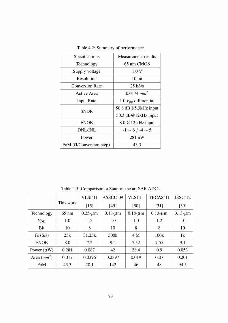
Table 4.2: Summary of performance
Specifications Measurement results
Technology 65 nm CMOS
Supply voltage 1.0 V
Resolution 10 bit
Conversion Rate 25 kS/s
Active Area 0.0174 mm2
Input Rate 1.0 Vpp differential
SNDR50.8 [email protected] input
50.3 dB@12kHz input
ENOB 8.0 @12 kHz input
DNL/INL -1 ∼ 6 / -4 ∼ 5
Power 281 nW
FoM (fJ/Conversion-step) 43.3
Table 4.3: Comparison to State-of-the art SAR ADCs
VLSI’11 ASSCC’09 VLSI’11 TBCAS’11 JSSC’12This work
[15] [49] [50] [31] [39]
Technology 65 nm 0.25-µm 0.18-µm 0.18-µm 0.13-µm 0.13-µm
VDD 1.0 1.2 1.0 1.0 1.2 1.0
Bit 10 8 10 8 8 10
Fs (S/s) 25k 31.25k 500k 4 M 100k 1k
ENOB 8.0 7.2 9.4 7.52 7.55 9.1
Power (µW) 0.281 0.087 42 28.4 0.9 0.053
Area (mm2) 0.017 0.0396 0.2397 0.019 0.07 0.201
FoM 43.3 20.1 142 46 48 94.5
79

4.4.3 Neural Signal Measurement
To verify the functionality of the proposed SAR ADC, simulated in-vitro [51,52] neural
signal recording is performed. The neural spike signal from rat brain was recorded after an
neural amplifier and digitized at 20 kS/s for 30 ms time interval. The pre-recorded discrete-
time neural signal is then stored in Tektronix 3022 arbitrary signal generator and fed into
the proposed SAR ADC. Figure 4.23 shows the pre-recorded neural spike signal and the
ADC output codes at 25 kS/s and 50 kS/s sampling rates, respectively. It can be seen that
the ADC output waveform preserves the characteristics of the pre-recorded neural spike.
0 5 10 15 20 25 30−0.02
0
0.02
0.04
Am
plitu
de (
V)
Pre−recorded neural signal
0 5 10 15 20 25 30−200
0
200
400
AD
C o
utpu
t
0 5 10 15 20 25 30−200
0
200
400
AD
C o
utpu
t
ADC output@ 25kS/s
ADC output@ 50kS/s
Figure 4.23: The pre-recorded neural spike signal and ADC output code. The X-axis is thenormalized time in ms. The ADC output data are normalized to the mid-code,511, to align with the pre-recorded neural spike.
4.5 Summary
This chapter presents a binary-weighted capacitor array SAR ADC prototype fabri-
cated in 65nm CMOS process. The ADC features a low-power and area-efficient switching
scheme. The proposed switching scheme is able to reduce the switching energy by 97%
and the capacitance area by 75% compared to the conventional switching scheme, which
80

have not been reported before. However, the proposed switching scheme increases the
digital circuit complexity, leading to some digital overhead. Thanks to the asynchronous
timing design, the proposed ADC employs TSPC DFFs in the digital circuit and the digi-
tal overhead is reduced and comparable to others. Some missing codes were observed in
the measurement results, which were caused by the settling issues in the first three largest
capacitors. This is expected to be solved by resizing the switches. The proposed ADC
occupies the smallest area while achieving a comparable FoM to many state-of-the-art de-
signs.
81

Chapter 5
A 6.2 fJ/c-s 9.0-ENOB 1MS/s SAR ADC
with Dynamic Latch based Digital
Controller
The previous two chapters investigated the unit-capacitor DAC array switching and binary-
weighted capacitor array tri-level switching schemes. The study on tri-level switching
scheme showed overall power saving capability of the ADC, and the ADC prototype demon-
strated both the low-energy and area-efficiency of this architecture. However, one short-
coming of the previous design is that the digital circuit complexity is increased compared
to conventional SAR ADC. Measurement results reveal that digital circuit consumes 55%
of the total ADC power consumption. The digital overhead can be resolved by redesigning
the switching network so that the number of DFFs is the same as the conventional counter-
part. To further reduce the power, a power-efficient digital controller is proposed to reduce
the digital circuit power consumption. The previous version of tri-level ADC suffered from
some missing codes due to DAC incomplete settling. In this design, the switch buffer sizes
are optimized to recover the missing codes. Besides that, a voltage controlled delay circuit
is also used for the critical delay element so that the internal clock period can be adjusted
for better DAC settling.
In this chapter, a new 10-bit SAR ADC targeted for biomedical applications is pre-
82

sented. The same design is fabricated in two CMOS technologies: Global Foundries (GF)
65nm CMOS process and UMC 65nm CMOS. The reason of using two different processes
is to compare the two technologies and to characterize the new GF process. Measurement
results show that the UMC prototype has much better performance than the GF prototype.
The final measurement results presented in the later part of this chapter, if not otherwise
stated, are all from the UMC prototype. The prototype ADC works from 0 to 1 MS/s.
The power consumption at 1 MS/s is about 3.252 µW, which is about half of the previous
prototype.
5.1 ADC Architecture
The architecture of the proposed SAR ADC is shown in Figure 5.1. The ADC still em-
ploys the tri-level switching scheme, which has already been discussed in last chapter. Just
like the previous design, the new ADC adopts asynchronous timing scheme and comprises
a differential capacitive DAC, a dynamic comparator, a delay-based internal clock gener-
ator. The novel dynamic latch-based digital controller requires fewer transistor count and
consumes less power compared to the TSPC DFFs. In addition, a small master reset circuit
is included to reset the dynamic circuits in order to reduce leakage current.
The function of the master reset circuit is to reset the entire ADC when conversion
is completed. This is especially important when the sampling speed is low. When the
proposed ADC is employed for some biomedical applications, the sampling speed could
be as low as 30 kS/s [53] for neural signal recording and 1 kS/s for ECG signal acquisition
[9, 39]. At such low sampling rate, the time between samples can be tens of µs to ms. The
proposed ADC can finish its conversion in a few hundred ns. After conversion, the ADC
would have large leakage current if the dynamic circuit is left floating. Figure 5.2 shows
the timing comparison of the previous design and the new design. The main difference is
the master reset signal in the new design. In Figure 5.2 (a), there is an idling mode after
the last bit is determined and before the rising edge of the Clks. When the ADC enters
idling mode, the leakage current in the digital circuit could discharge the gate parasitic
83

Delay-based
Internal
clock
generator
Novel Dynamic
Latch based digital
controller
Vref
Vref
Vcm
Vcm
Valid
…...
D0 D1 D8 D9
Sampling clock,
Clks
Comp_clk
DOL (Digital Output
Logic)
…...
Von
Vop
GND
GND
VINP
VINN
C0UC1UC7UC8U
C8L C7L C1L C0L
Bootstrapped
Master
Rst
EoC
Rst
Rst
Figure 5.1: Architecture of the ADC with low-power digital controller.
capacitance of the dynamic digital logic if no action is taken. If the idling time is long
enough, some of the digital circuit may begin conducting and result in huge short circuit
current. For example, the gate voltage of a dynamic inverter could be discharged to VDD2
when both NMOS and PMOS are turned on. The time for ADC in idling mode depends
on the sampling rate as well as the duty ratio of the Clks signal. For the previous design,
the duty cycle of the system clock Clks must be adjusted at different sampling rates such
that the idling time is as short as possible for all cases. This is to make sure that the digital
circuit is immediately reset after the last bit is resolved. In such way the leakage current
is minimized. For a standalone ADC design, this simple method is manageable because
the duty cycle of the system clock can be easily adjusted by FPGA or some other clock
generation device. However, this method faces difficulty in system level design when the
ADC is integrated in a whole biomedical system. In a complete system, the duty cycle of
the system clock can not be easily adjusted precisely when the ADC sampling rate changes.
In the new design, this problem is solved by adding the master reset circuit that imme-
diately generates the Master rst signal after the last bit, as shown in Figure 5.2 (b). With
84

Clks
Comp_clk
EOC
ADC output
Conversion Sampling
& Reset
Conversion
Clks
Comp_clk
EOC
ADC output
ConversionResetMaster_rst
Sampling(a)
(b)
Idling
Figure 5.2: (a) The timing diagram of the previous design and (b) The timing diagram ofthe new design.
the Master rst signal, the idling mode is completely eliminated. The digital circuit directly
enters the reset state. Therefore, the leakage current can be minimized. The restriction on
the system clock duty cycle is also removed.
5.2 Circuit Implementations
The circuit implementations for both GF process and UMC process are very much
the same. The only difference is in the capacitor array. Hence, the capacitor array for
both designs are discussed in depth in this section. Other building blocks are discussed in
general since they are the same for both designs in the two technologies.
5.2.1 Capacitor Array Design in GF 65nm CMOS
The GF 65nm CMOS process provides 6 layers of level-1 metal, 2 layers of level-2 (2X
thickness) metal in low-k and 1 layer of level-4 (4X thickness) metal. In the PDK library,
two types of capacitor are available, namely the Metal-Insulator-Metal (MIM) capacitor
85

and MOM capacitor. The MIM capacitor provided by foundry can only be accessed from
the top-level (4X) metal. The top-level metal is very wide and requires a large spacing to
the neighboring top-level metal by DRC rule. This makes the MIM capacitor unsuitable for
DAC capacitor array design. As for the MOM capacitor, the number of fingers for the top-
plate and bottom-plate is the same and no bottom-plate metal shielding is implemented. As
a result, the top-plate parasitic capacitance is too large for DAC array design. In addition,
the MOM capacitor must be covered by a labeling marker layer in layout. The layout
rule requirement for the marker layer demands a large distance between the neighbouring
capacitors. This makes the capacitor matching very poor. Since the capacitors provided
by foundry are not suitable for DAC capacitor array design, customized capacitors are
designed for the GF process.
The customized capacitor must satisfy two basic requirements. Firstly, the capacitor
size must be small. The DAC capacitor array occupies most of the area in a SAR ADC.
Minimizing the capacitor size reduces the overall ADC area. In addition, smaller DAC
capacitor array area means better matching among the capacitors. Secondly, the top-plate
parasitic capacitance must also be as small as possible. Since the tri-level switching scheme
samples the input voltage on the top-plate of the DAC capacitor array, the top-plate parasitic
capacitance reduces the DAC voltage swing and introduces gain error. Minimizing the top-
plate parasitic capacitance is the most straight forward method to alleviate the problem.
Since no information is available about the customized capacitor matching, the size of the
unit capacitor is chosen to be the same as the previous design, 10 fF. Both MIM and MOM
capacitors are design for comparison.
Figure 5.3 shows the designed multi-layer MIM capacitor. The grey area represents the
top-plate, which is made of M3 and M5. The bottom-plate is made of M2, M4 and M6.
The top-plate is enclosed by the bottom-plate so that the top-plate parasitic capacitance is
minimized. The size of the MIM capacitance is 4.03 µm × 4.03 µm and the capacitance
is around 10.55 fF given by the parasitic extraction tool. M1 is not used in the capacitor
design for two reasons. Firstly, M1 is reserved for bottom-plate routing. Secondly, the
86

bottom-plate parasitic capacitor will be very large if M1 is used in the bottom-plate design.
Although the bottom-plate parasitic capacitance does not degrades ADC performance, it
increases the power consumption. Since M6 is available in this process, upper level metal
layers are used to design the capacitor.
M6
M5
M4
M3
M2
VIA56VIA45
VIA56VIA45
VIA34VIA23
VIA34VIA23
M4
VIA45VIA34
(a) (b)
Figure 5.3: (a) Top view of the customized MIM capacitor (b) Cross section view of thecustomized MIM capacitor.
Figure 5.4 shows the top view and cross-section perspective view of the customized
MOM capacitor. MOM capacitors rely on the coupling capacitance between the metal
fingers running in parallel. Metal layers are stacked from M2 to upper metal layer to
increase the capacitance. The grey area shown in Figure 5.4 (a) is the top-plate, and it is
clear that the top-plate is surrounded by the bottom-plate. As shown in Figure 5.4 (b), M2
is solely used for the bottom-plate design to shield the top-plate. This is the same reason
as for MIM capacitor design to minimize the top-plate parasitic capacitance. Metal finger
width and spacing are fixed at the minimum dimensions, 0.1 µm, to achieve the maximum
capacitance density. The MOM capacitor size is 3 µm × 2.5 µm, having a capacitance of
10.11 fF.
Unlike the previous chip which keeps the differential capacitor arrays together, the two
DAC capacitor arrays in the current design are placed away from each other to make the
routing easier and avoid interference. Figure 5.5 shows the layout floor plan of the DAC
capacitor array. Common-centroid layout strategy is adapted for better matching. The
87

M2
M3
M4
M5
M6
(a) (b)
Figure 5.4: (a) Top view of the customized MOM capacitor (b) Cross section view of thecustomized MOM capacitor.
capacitors C4 to C0 are highlighted in the figure.
Two SAR ADCs using the same architecture are fabricated in GF 65nm CMOS to
investigate the effect of using customized MIM and MOM capacitors. A top-level parasitic
extraction is done on both ADCs after layout to verify the parasitics and confirm proper
binary scaling of the capacitor array. Table 5.1 shows the extracted parasitic capacitance
and their normalized values for both MIM and MOM DAC capacitor arrays. The binary
scaling is not perfectly achieved for both types of capacitor arrays. The MIM capacitor
array seems to have better extracted capacitance values than the MOM capacitor array. The
discrepancy of capacitors ratio for both MIM and MOM capacitor arrays reflects how the
foundry models the coupling capacitance between two metals. As for this design, no action
was taken to correct the discrepancy.
The capacitor ratio discrepancy shown in Table 5.1 has the same effect as the actual
capacitor mismatch after fabrication. A rough estimation by subtracting the actual ratio to
the ideal ratio reveals that the capacitor ratio discrepancy is equivalent to a 0.4% capacitor
mismatch for MIM capacitor array and 1% capacitor mismatch for MOM capacitor array.
By taking the σINL,max and σDNL,max derived in the previous chapter, the equivalent 0.4%
and 0.1% capacitor mismatch yields σDNL,max of 0.256 LSB for MIM capacitor array and
0.64 LSB for MOM capacitor array. These results indicate the capacitor ratio discrepancy
88

8 8
8 8
7 7
7 7
6 5
6 5
5 6
5 6
8 8
8 8
7 7
7 7
6 5
6 5
5 6
5 6
8 8
8 8
7 7
7 7
6 4
6 4
4 6
4 6
8 8
8 8
7 7
7 7
6 3
6 3
3 6
3 6
8 8
8 8
7 7
7 7
6 2
6 1
2 6
0 6
8 8
8 8
7 7
7 7
6 4
6 4
4 6
4 6
8 8
8 8
7 7
7 7
6 5
6 5
5 6
5 6
8 8
8 8
7 7
7 7
6 5
6 5
5 6
5 6
D D D D D D D D D D D D D D D
D D D D D D D D D D D D D D D D
8 8
8 8
8 8
8 8
8 8
8 8
8 8
8 8
8 8
8 8
8 8
8 8
8 8
8 8
8 8
8 8
8 8
8 8
8 8
8 8
8 8
8 8
8 8
8 8
8 8
8 8
8 8
8 8
8 8
8 8
8 8
8 8
8 8
8 8
8 8
8 8
8 8
8 8
8 8
8 8
8 8
8 8
8 8
8 8
8 8
8 8
8 8
8 8
7 7
7 7
7 7
7 7
7 7
7 7
7 7
7 7
7 7
7 7
7 7
7 7
7 7
7 7
7 7
7 7
D
D
D
D
D
D
D
D
D
D
D
D
D
D
D
D
DD
D
D
D
D
D
D
D
D
D
D
D
D
D
D
D
D
DD
D
1 0
Figure 5.5: Floor plan for the capacitor array.
Table 5.1: Extracted capacitors and their normalized value
CapacitorsMIM Capacitor Array MOM Capacitor Array
Value (fF) Normalized Value Value (fF) Normalized Value
C0 10.55 1 10.11 1
C1 10.55 1 10.11 1
C2 21.05 1.995 20.13 1.991
C3 42.11 3.991 40.24 3.980
C4 84.17 7.978 80.37 7.950
C5 168.2 15.943 160.5 15.875
C6 336.3 31.877 320.1 31.661
C7 673.8 63.867 640.9 63.393
C8 1345 127.488 1281 126.706
89

is not large enough to cause ADC missing code.
5.2.2 Capacitor Array Design in UMC 65nm CMOS
The ADC designed in UMC 65nm CMOS technology directly uses MOM capacitors
provided by the PDK. For the previous prototype design in the same technology, the unit
capacitance was 10 fF. This value was obtained from the derived worse-case DNL expres-
sion. However, the derived formula exaggerates the worse-case DNL as discussed in the
previous chapter. Hence, a smaller unit capacitor is adopted for this new design.
The measurement results of the previous chip showed DNL for most of the codes is
within +/- 0.5 LSB despite some missing codes, which were caused by the non-optimized
switch buffer. That indicates that the 10 fF unit capacitor has good enough matching for
10-bit accuracy. Therefore, the unit capacitance is chosen to be 7 fF for this design. The
size of the unit capacitance is 2.1 µm × 2.7 µm.
5.2.3 Dynamic Comparator
The dynamic comparator used in the previous design has a pair of isolation transistors
in the first stage to reduce the kick-back noise. However, the isolation transistors forced
the differential pair transistors to go from saturation into triode region. Hence, the effective
gain of the first stage is reduced. In order to solve this problem, the current in the first stage
is designed to be relatively large. On top of this, a pair of inverters are placed between the
first and second stages to provide some additional gain. These methods inevitably increase
the comparator power consumption, which accounts for 23% of total power. A modified
dynamic comparator similar to [27, 46] is adopted in this design, as shown in Figure 5.6.
The comparator is designed with high-VT and regular-VT devices to minimize the leakage
current while maintaining the speed. In addition, the comparator uses the outputs of the first
stage to reset the second stage, eliminating the complementary clock signal as in [27, 46].
The same comparator is used in the GF 65nm design and UMC 65nm design. For the
GF 65nm CMOS process, the offset voltage of the comparator is unknown because the
90

CLK
CLK
Vinp Vinn
Vo_d1 Vo_d2
Vo_d1 Vo_d2
OUTN
OUTP
HVT
HVT HVT
HVT HVT
PMOS: 0.4u/0.2u
NMOS: 4u/0.2u (Diff. pair), 0.2u/0.1uPMOS: 0.4u/0.2u
NMOS: 4u/0.2u
Figure 5.6: The high-speed low-leakage dynamic comparator.
statistical library is not available. The static offset is due to the transistor threshold voltage
mismatch and mobility mismatch. The dynamic offset is caused by the output capacitance
mismatch [54], which can be minimized by careful layout. Symmetrical layout instead
of the common-centroid layout technique is adopted for the comparator layout, as shown
in Figure 5.7. Dummy transistors are used for the critical transistors in layout. In order
to balance the output nodes parasitic capacitance, dummy metal is also implemented to
balance the coupling capacitance. For the GF 65nm design, the parasitic capacitances at
the two branches of the first stage output as well as the second stage output are kept close to
each other. The parasitic capacitance at Vo d1 and Vo d2 due to the metal routing are 409.2
aF and 409.3 aF, respectively. The parasitic capacitance at the second stage output OUTP
and OUTN are obtained as 413.5 aF and 413.2 aF, respectively. Post-layout simulations
reveal that the comparator can resolve a small input difference as low as 50 µV.
For the UMC 65nm design, the parasitic capacitance of the first stage output nodes
are 116 aF and 115.7 aF, and for the second stage output nodes are 210.4 aF and 209.3
aF, respectively. Hence, the dynamic offset has been minimized. Monte-carlo simulations
were performed at different common-mode voltages to determine the static offset voltage
variations. Figure 5.8 shows the mean and standard deviation of the offset voltage in the
UMC design. As discussed in previous chapter, a fixed comparator offset voltage does not
affect the ADC performance, but the change of comparator offset voltage over different
91

6.5 µm
10
µm
6.7 µm
12 µ
m
(a) (b)
Figure 5.7: Layout of the comparator in (a) GF 65nm CMOS process and (b) UMC 65nmCMOS.
common-mode voltage will deteriorate the linearity and introduce distortion. As shown
in Figure 5.8, the comparator offset voltage change is relatively small for Vcm below 0.85
V while a larger offset voltage variation is expected for Vcm above 0.85 V. For the worst-
case 3σ scenario, the offset voltage variation can be 6.5 mV, which corresponds to 3.5
LSB. This means that the worst-case DNL due to the comparator offset is about 3.5 LSB
at the two end of the output digital code according to the approximated DNL expression
DNL = ∆Vactual∆Videal
−1 ≈ ∆Vo f f set∆Videal
= ∆Vo f f set LSB in section 4.2.2 of the previous chapter. The
3.5 LSB DNL error is the worse-case scenario and will definitely cause some missing codes
towards two ends of the digital codes and introduce distortion to the ADC performance.
Unfortunately it could not be completely resolved by comparator offset calibration due
to the changing of input common-mode voltage. Nevertheless, one way to mitigate the
problem is to use a pre-amplifier as the comparator first stage. However, the biasing current
in the pre-amplifier will inevitably increase power consumption.
92

0.5 0.6 0.7 0.8 0.9 1
0
0.2
0.4
0.6
0.8
Off
set M
ean
valu
e (m
V)
0.5 0.6 0.7 0.8 0.9 14
5
6
7σ
(mV
)
Vcm
(mV)
Figure 5.8: Simulated comparator offset voltage mean and standard deviation at differentinput common-mode voltage.
5.2.4 Internal Clock Generation Circuit with Master Reset
Figure 5.9 shows the internal clock generation circuit together with master reset cir-
cuit. The internal clock generation circuit is simplified to two AND gates and a voltage-
controlled delay cell. As compared to the previous design, which consists of one XOR
gates, two AND gates and two delay cells, further power was saved in this version. In addi-
tion, the delay cell is made voltage dependent such that an optimum delay can be selected.
The master reset circuit is very crucial for low-to-medium speed operation, as discussed
earlier and it can be implemented with just one DFF and one OR gate. Note that the DFF
in the master reset circuit must be implemented by conventional static DFF instead of any
dynamic circuits, such as TSPC DFF. The reason is that the DFF works at the same speed as
the ADC sampling rate, which could be low for some applications, but dynamic circuit will
not be able to work at such speed. The DFF and OR gate in the master reset circuit only
toggle twice in one ADC conversion cycle. The power consumption of the master reset
circuit is very small compared with the internal clock generation circuit, which generates
10 clock cycles.
The working principle of the circuit can be easily understood by considering the tim-
93

Comparator
Voltage-
controlled
delay cell
Q
QSET
CLR
D
Clks
Clksb
Clksd
EoC
Q Master_rstMaster_rstb
VTC
Master reset
circuit
Internal clock generation circuit
Valid
Static DFF
Figure 5.9: The internal clock generation and master reset circuitry.
ing diagram in Figure 5.10. The Clks signal is the system clock, which is also the ADC
sampling rate. The Clksb and Clksd signals are the complementary and the delayed Clks
signal. These two signals control the bootstrapped switches. Clksb also resets the DFF.
The ADC conversion starts when Clks goes low. Since Q is low, Master rstb becomes
high. The rising edge of Master rstb triggers the first pulse of the Comp clk signal. After
10 pulses are generated, the SAR logic sends the EoC signal. The rising edge of EoC
triggers the DFF and Q becomes high. As a result, Master rstb goes low and Master rst
goes high. These two signals reset the ADC.
5.2.5 Switch Buffer Configuration
In the previous deign, the switch buffer needs three control signals, which must be
generated separately. In this design, the switch buffer is modified so that only two control
signals are needed. This simple modification can save one third of DFFs. Figure 5.11
shows the simplified switch buffer schematic. One more transmission gate is added to the
inverter switch, M1 and M2. The two TG switches, TG1 and TG2, need only one control
signal and work complementarily. When TG1 that is connected to Vcm is turned on, TG2
is turned off. In this case, the bottom-plate of the capacitor is connected Vcm only. When
94

Clks
Comp_clk
EoC
ADC output
Master_rst
Clksd
Clksb
Q
Master_rstb
Figure 5.10: The simplified timing diagram of the internal clock generation circuit.
TG1 is turned off, TG2 is turned on. The bottom-plate of the capacitor can be connected
to either Vre f or ground, depending on the previous bit decision. With this modified switch
buffer, the NMOS and PMOS in the inverter can be controlled by the same signal. Only
two control signals are needed. Hence, power and area reduction are achieved for the SAR
logic circuit.
S8nS8cm
Vcm
M1 M2M3M4
C8
S7nS7cm
Vref
M5 M6M7M8
C7
S8cm S8cmbS7cm S7cmbTG1
TG2
Figure 5.11: The switch buffer design for the capacitor array.
95

5.2.6 Novel Latch-based Digital Controller
The SAR digital controller in the previous prototype was implemented by TSPC dy-
namic DFFs. In this design, a customized digital controller based on dynamic latch is
proposed. The proposed digital controller uses less transistors than the TSPC DFF cell to
implement the same function. Therefore, power reduction is expected.
Figure 5.12 shows the block diagram of the proposed SAR digital controller. The SAR
logic performs binary search algorithm in 10 identical cycles. The SAR controller consists
of two parts, the main control logic and the DAC control logic. The main control logic is
implemented with simple dynamic logic gates and the DAC control logic is the dynamic
latch. It can be seen that only five signals are supplied to the SAR digital controller, namely
Valid, Master rst, Master rstb, VOP and VON. The Master rst signal is the reset signal for
the main control logic circuits. Master rstb is the complementary of Master rst and used to
trigger the first dynamic latch. VOP and VON are comparator output signals that determine
the ADC output bit and generate the correct DAC control signals. Valid is the internal clock
signal for the main control logic circuits and it is generated from VOP and VON.
Valid
Master_rst
VOP
VON
DAC control
Main control
Master_rstb
EN
Rst OUTP
OUTN
Valid K
En_next
Trig_next
Trig
OUTP
OUTN
VOP
VON En_next
EN
Rst OUTP
OUTN
Valid K
En_next
Trig_next
Trig
OUTP
OUTN
VOP
VON En_next
EN
Rst OUTP
OUTN
Valid K
En_next
Trig_next
Trig
OUTP
OUTN
VOP
VON En_next
EN
Rst OUTP
OUTN
Valid K
En_next
Trig_next
Trig
OUTP
OUTN
VOP
VON En_next
...
...
EoC
S8cm S1cm
S0cm
S8pS8n S7pS7n S0pS0n
...
Figure 5.12: Block diagram of the SAR logic controller.
96

The SAR logic circuit performs one-bit cycle operation at every rising edge of com-
parator clock. The one-bit cycle operation can be illustrated with the state machine diagram
shown in Figure 5.13. Firstly, a comparison is performed at the rising edge of compara-
tor clock (1). The comparator output signals feed into the clock generation circuit (2) to
produce Valid signal (3). At the same time, they are also stored in the dynamic latch (4).
When the latch output signals are available, the main control logic enables the next slice of
the main control logic (5). At the falling edge of the Valid signal, the next slice of dynamic
latch is triggered (6). When the next comparator clock rising edge comes, the same process
will be repeated in the next slice of main control logic and dynamic latch circuits.
Comparator trigger (1)
Comparator output (2),
VOP,VON
Valid Signal (3),
Valid
Latch output (4),
OUPT,OUTN
Enable Next slice (5),
En_next
Trigger the next dynamic
latch (6), Trig_next
Figure 5.13: The conceptual state machine of one-bit cycle.
In the proposed SAR ADC, above six steps are synchronized to the internal comparator
clock signal. This is shown by the simplified timing diagram in Figure 5.14. Each rising
edge of the comp clk signal indicates the beginning of one-bit cycle. When the present
comparator output signals are stored in the latch, the En next signal is initiated and the
next-bit digital circuits are enabled. In addition, the trig next signal in step (6) is initiated
by the falling edge of Valid. In other words, the next slice of digital circuit for the next one-
bit cycle operation has already been enabled and triggered before the present one-bit cycle
97

operation is finished. Hence, the main control and DAC control circuits must be carefully
designed to minimize leakage current. This will be discussed in the following paragraphs.
Comp_clk
VOP
VON
Valid
OUTP(i)
OUTN(i)
En_next(i)
Trig_next(i)
(1)
(2)
(3)
(4)
(5)
(6)
Present bit Next bit
OUTP(i+1)
OUTN(i+1)
K(i)
K(i+1)
Figure 5.14: The timing diagram of one-bit cycle.
Figure 5.15 shows the main control logic circuit gate-level design as well as the transistor-
level implementation. Only 11 transistors are used to implement the main control logic cir-
cuit, with the timing diagram shown in Figure 5.14. The enable signal, EN, is the En next
from the previous cycle. Since the PMOS transistors controlled by OUTP and OUTN re-
main off, there will be no current in the NOR gate even when En is low in the previous
cycle.
Figure 5.16 shows the schematic of the dynamic latch for the DAC control circuit and
its timing diagram. Dynamic latch has shown excellent power efficiency [54] in many low-
power applications, as there is no static current in any branch of the circuit at any time.
It works by charging or discharging the parasitic capacitance at the output nodes. The
simplified timing diagram of the dynamic latch can be divided into three phases as shown
in Figure 5.16 (b). In phase 1, the trig signal is low. The latch is in reset phase and NMOS
98

Rst
EN
KEn_next
Valid
Trig_next
Rst
ENOUTP
OUTN K En_next
(b)(a)
OUTP OUTN
Valid
Trig_next
EN
Figure 5.15: (a) The gate-level design of the main control circuit and (b) Transistor levelimplementation.
M5 is turned off. Although either VOP or VON toggles with the comparator clock, the
parasitic capacitance is not charged during this phase. Hence the power consumption in
this phase is very small. In phase 2, trig signal becomes high. In this phase, the PMOS
transistors M6, M7 and the reset transistors are all turned off. NMOS M3, M4 and M5 are
turned on. However, VOP and VON derived from the comparator output signals are low.
Trig
VOP VON
OUTN OUTP
En_Next
M1 M2
M3 M4
Comp_clk
VOP
VON
Trig
Previous cycle Present cycle
En_next
OUTP
OUTN
M5
M6 M7
(a) (b)
Phase 1 Phase 2 Phase 3
M8 M9
Figure 5.16: (a) Schematic of the dynamic latch for the DAC control logic (b) The timingdiagram.
99

No conducting path exists in this phase. In phase 3, when either VOP or VON goes high,
one of the the latch output OUTP or OUTN will be discharged to ground and the other one
remains high. Once the comparator output is stored in the latch, the En next signal turns
low. This turns off M3 and M4.
Since comparator output signals VOP and VON keep switching transistor M1 and M2
on and off, NMOS M3 and M4 must be added to isolate the latch output nodes, OUTP and
OUTN, from M1 and M2. This is to avoid the possibility of discharging the latch output
nodes through M1 and M2. Taking the signals in Figure 5.16 (b) for an example, OUTN
remains high and OUTP is discharged to ground for the present bit-cycle since comparator
output VON is “1” and VOP is “0”. These values are stored in the latch for the moment.
In the following bit-cycles, the comparator output signals change as the comparator clock
signal. It is possible that M1 is turned on by VOP and latch output OUTN is discharged
to ground if M3 are M4 are not added. This will alter the stored digital value and cause
the SAR logic to switch the corresponding capacitor to the wrong value. Hence, the ADC
output results will be completely wrong in this case. With M3 and M4 switched off by
En next, this problem is avoided. The reset transistors M5, M8 and M9 are implemented
by High-VT devices to reduce leakage current.
5.3 Simulation Results
In general, the linearity simulation does not have much meaning regarding ADC perfor-
mance since the capacitor mismatch model was not invoked. In addition, a large number of
samples are required in order to obtain accurate linearity information [55], which is infeasi-
ble to perform in simulations. Similarly, the dynamic simulation only reveals the distortion
introduced by the charge-injections and parasitics. To save simulation time, the transient
noise was not enabled. Hence, static and dynamic simulations were performed for both
designs only to ensure there was no missing codes caused by any design mistakes.
Figure 5.17 shows the simulated 1024-point FFT plot for the MIM capacitor ADC
designed in GF 65nm CMOS technology. The ADC was simulated at 1 V supply and 1
100

MS/s. 0.5 bit was lost due to the DAC parasitic capacitance. No missing code was observed
because there was no obvious harmonic distortion.
0 1 2 3 4 5
x 105
−120
−100
−80
−60
−40
−20
0
Frequency (Hz)
Pow
er (
dB)
SNR: 59.6 dBSNDR: 59.2 dBSFDR: 76.73 dBENOB: 9.55 bit
Figure 5.17: The simulated 1024-point FFT output spectrum of ADC designed in GF 65nmCMOS technology.
The chip designed in UMC 65nm technology was also simulated and Figure 5.18 shows
the simulated 2048-point FFT output spectrum. The number of FFT points does not affect
the simulation results drastically. The 2048-point FFT has higher frequency resolution on
the FFT plot and increases the accuracy of simulated noise level. It seems that the design in
UMC process has slightly better performance in simulation than the design in GF process.
5.4 Measurement Results
Figure 5.19 shows the die photo and ADC layout in the GF 65nm CMOS and UMC
65nm CMOS design, respectively. ADC area is 185 µm × 100 µm in GF design and 140
µm × 90 µm in the UMC design. Both designs have similar layout floor plan for the
building blocks, such as comparator, capacitor array, switches, and so on. In this section,
some measurement results from both designs are presented.
101

0 100 200 300 400 500−120
−100
−80
−60
−40
−20
0
Frequency (kHz)
Pow
er (
dB)
SNR: 61 dBSNDR: 60.69 dBSFDR: 75.74 dBENOB: 9.79 bit
Figure 5.18: The simulated 2048-point FFT output spectrum of ADC designed in UMC65nm CMOS technology.
5.4.1 GF 65nm CMOS Chip Results
The prototype was tested at 1 V supply voltage and under different sampling rate, rang-
ing from 1 kS/s to 1 MS/s. However, the results are not promising. A lot of missing codes
100
µm
185 µm
90
µm
140 µm
(a)
(b)
Cap array
SAR Logic
Bootstrapped switchcomparator
Cap arrayMIM cap
ADC
MOM cap
ADC
Figure 5.19: (a) ADC die photo and layout in GF 65nm CMOS design (b) ADC die photoand layout in UMC process design.
102

were observed in static test. Figure 5.20 and 5.21 plot the output FFT spectrum of the MIM
capacitor ADC and MOM capacitor ADC in GF 65nm CMOS technology, respectively.
It also confirmed for multiple samples that customized MOM capacitor array has better
matching than the customized MIM capacitor array.
0 10 20 30 40 50−120
−100
−80
−60
−40
−20
0
Frequency (kHz)
Pow
er (
dB)
SNR: 37.4 dBSNDR: 36.62 dBSFDR: 48.9 dBENOB: 5.8 bit
Figure 5.20: Measured FFT spectrum of the MIM capacitor ADC in GF process.
0 10 20 30 40 50−120
−100
−80
−60
−40
−20
0
Frequency (kHz)
Pow
er (
dB)
SNR: 40.48 dBSNDR: 39.10 dBSFDR: 48.26 dBENOB: 6.2 bit
Figure 5.21: Measured FFT spectrum of the MOM capacitor ADC in GF process.
The missing codes are most probably caused by device mismatch in the capacitor array
and dynamic comparator. The customized capacitor cell does not have sufficient matching
for 10-bit accuracy. Either calibration or a much larger unit capacitor can be adopted to
103

improve the ADC performance. However, power and area overhead is unavoidable. The
comparator offset voltage changes with input common-mode voltage. The change in the
comparator offset voltage over Vcm will cause missing codes if the offset voltage variation
is too large.
5.4.2 UMC 65nm CMOS Chip Results
The chip designed in UMC 65nm CMOS technology was measured at 1 V supply and
1 MS/s. Figure 5.22 shows that the measured DNL is within -0.69/0.58 LSB and INL is
within -0.96/1.17 LSB. This confirms that the missing codes from previous prototype was
caused by the switch buffer and can be recovered. The INL is obtained by best-fit line [56]
after correcting the gain error and offset error. The positive peak INL error at the lower end
of output codes is caused by the comparator offset and the negative peak INL around the
middle of output codes is caused by the variation of Vcm voltage. The gain error is about
-0.05% and the offset error is about -0.25 LSB.
0 200 400 600 800 1000−1
−0.5
0
0.5
1
DN
L (L
SB
)
0 200 400 600 800 1000−1
−0.5
0
0.5
1
1.5
Code
INL
(LS
B)
[−0.69, +0.58]
[−0.96, +1.17]
Figure 5.22: Measured INL and DNL at 1MS/s. The INL is obtained by best-fit line.
Figure 5.23 shows the output spectrum for a near-DC and a near-Nyquist tones, re-
spectively. The amplitude of test stimulus for both tests was set to -0.4 dBFS. The ENOB
equals 9.03 bit, while the ERBW is slightly beyond Nyquist. When the input signal fre-
quency is near-Nyquist, a 0.08 bit ENOB-loss is observed. The 2nd-harmonic power has
104

slightly higher power than the 3rd-harmonic. This is due to the pseudo-differential nature of
the tri-level switching scheme and the 2nd-order harmonic cannot be completely removed
at higher signal frequency.
0 100 200 300 400 500
−100
−50
0
Frequency (kHz)
Pow
er (
dB)
0 100 200 300 400 500
−100
−50
0
Pow
er (
dB) Signal frequency: 44.7998 kHz
SNDR: 56.12dB, SFDR: 67.37dB, ENOB: 9.03bit
Signal frequency: 490.6 kHzSNDR: 55.62dB, SFDR: 67.38dB, ENOB: 8.95bit
Figure 5.23: 8192-point FFT output spectrum for 44.7998 kHz and 490.6 kHz input sig-nals.
Figure 5.24 plots the measured SNR, SNDR, SFDR and THD values versus the input
signal frequency at 1 MS/s. The SNR is relatively flat for all the input signal frequency
range. The SFDR variation is within 3 dB over the input frequency range. The THD,
which is dominated by the 2nd and 3rd-order harmonics, changes with the SFDR.
The maximum frequency at which the ADC can operate depends on the internal clock
frequency and the required sampling time. The internal clock frequency can be tuned
manually to determine the best ADC performance. For this measurement, the internal
clock period is tuned to about 26 ns, which gives 260 ∼ 270 ns for 10-bit ADC conversion
time. As for the sampling time, the on-resistance of the bootstrapped switch is about 167
Ω and the DAC capacitance is 1.792 pF. Hence the RC time constant is τ = 0.3 ns. The
voltage sampled on DAC during sampling phase is given by: VDAC (t) =Vin[1− exp
(− t
τ)]
.
For DAC to settle down to 10-bit accuracy in sampling phase, the sampling time should be
longer than 8τ , 2.4 ns. As a result, the maximum operating speed of the ADC can go up
105

0 100 200 300 400 50050
55
60
65
70
75
Frequency (kHz)
SNR
,SN
DR
,SFD
R &
|TH
D| (
dB)
SNRSNDRSFDRTHD
Figure 5.24: Dynamic performance at different input signal frequencies.
to 3 MS/s. For this measurement, the ADC is characterized from 1 kS/s to 2 MS/s. Figure
5.25 shows the SNDR of the ADC measured at different sampling speeds for input signal
frequency ranging from near-DC to near-Nyquist. It can be seen that the SNDR variation
over the input signal frequency range at different sampling rates is less than 2 dB. This is
the nature of the proposed timing scheme, which allows the ADC to finish its conversion
in a fixed small time interval even through the sampling speed changes.
The power consumption is also measured for different sampling rates. Figure 5.26
shows the ADC ENOB, Power consumption and FoM at different sampling rates. The
ENOB variation is 0.12 bit. For sampling speed higher than 25 kS/s, the power consump-
tion scales almost linearly with the sampling frequency. The leakage current is about 40
nA, which dominates the power consumption for sampling rate lower than 10 kS/s. The
ADC achieves its best FoM, 6.22 fJ/Conversion-step, at 500 kS/s and 1 MS/s. Table 5.2
summarizes the detailed power, ENOB and FoM for all tested sampling frequencies.
The power consumption of individual building blocks is simulated. Table 5.3 shows the
distribution of the power consumption for each building block obtained in simulations at
1 MS/s. The power consumption for parasitics in the last column is estimated by simply
106

0 0.1 0.2 0.3 0.4 0.552
54
56
58
Normalized input frequency (fin
/fs)
SND
R (
dB)
2MS/s1MS/s100kS/s10kS/s
Figure 5.25: SNDR at different input signal frequencies for different sampling rates.
103
104
105
106
8.9
8.95
9
9.05
9.1
EN
OB
(bi
t)
103
104
105
106
10−8
10−6
10−4
Pow
er (
W)
103
104
105
106
0
50
100
FoM
(fJ
/C−
S)
Sampling frequency (Hz)
Best FoM: 6.22 fJ/C−S
Leakage current ~ 40nA
Figure 5.26: The ENOB, power consumption and FoM for different sampling rates.
107

Table 5.2: Measured ADC Power and FoM at different sampling frequencies
Sampling Rate (S/s) Power Consumption ENOB (Bit) FoM (fJ/C-S)1k 54 nW 8.92 92.9
10k 75 nW 8.97 15
25k 100 nW 9.02 7.7
50k 210 nW 9.0 8.2
100k 340 nW 9.03 6.5
200k 665 nW 9.04 6.32
500k 1.64 µW 9.04 6.22
1M 3.25 µW 9.03 6.22
2M 6.5 µ W 8.98 6.44
subtracting the schematic-based results from the post-layout simulation results. It can be
seen that the parasitics in the digital circuit consumes almost three times of the power
consumed by the digital circuitry itself. The parasitics in the analog circuits contribute to
only a small percentage of the power consumption. The large amount of power consumed
in the digital circuit parasitics can be reduced by optimizing the layout.
Table 5.3: Simulated Power Consumption at 1 MS/s
Component Schematic (µW) Post-layout (µW) Parasitics (µW)Capacitor Array 0.364 (21.9%) 0.43 (14 %) 0.066 (4.7%)
Comparator 0.635 (38.2%) 0.74 (24.1%) 0.105 (7.4%)
SAR Logic 0.205 ( 12.3%) 0.668 (21.7%) 0.463 (32.8%)
Internal Clock Gen. & Others 0.46 (27.6%) 1.238 (40.2%) 0.778 (55.1%)
Total 1.664 3.076 1.412
A summary of the measured performance is given in Table 5.4. Table 5.5 compares
the measurement results of this work to previously published SAR ADCs with comparable
sampling rates and similar technology. The proposed ADC has the smallest area compared
to other ADCs fabricated in 65 nm technology. It is even comparable to the ADC designed
in 40 nm CMOS technology [57]. The ADC achieves a good FoM compared to the state-
108

of-the-art designs.
Table 5.4: Specification summary
Specifications Measurement resultsTechnology 65 nm CMOS
Supply voltage 1.0 V
Resolution 10 bit
Conversion Rate 1MS/s
Active Area 0.0124 mm2
Input Rate 2.0 Vpp differential
INL (LSB) - 0.96 ∼ 1.17
DNL (LSB) - 0.69 ∼ 0.58
SNDR (dB) 56.12
SFDR (dB) 67.37
THD (dB) - 64.67
ENOB 9.03
Power (µW) 3.252
FoM (fJ/Conversion-step) 6.22
Offset Error (LSB) - 0.25
Gain Error - 0.05%
Figure 5.27 shows the power efficiency comparison of state-of-the-art SAR ADC and
this work. The proposed ADC is one of the designs that achieve very good FoM for sam-
pling rate higher than 1 MS/s. Figure 5.28 plots the area versus power efficiency for state-
of-the-art SAR ADC and this work. The proposed SAR ADC is one of the several ADCs
that have both small area and high power efficiency.
5.5 Summary
In this chapter, a low-power SAR ADC with dynamic latch based digital controller was
designed and implemented in two 65 nm technologies, namely the GF 65 nm CMOS and
UMC 65 nm CMOS. With the simplified digital controller, the ADC power is improved
over 50% compared to prior design. The ADC performance in terms of power efficiency
109

Table 5.5: Comparison to State-of-the art
JSSC’13 JSSC’12 JSSC’12 ESSCIRC’12 JSSC’10This work
[58] [57] [45] [59] [27]
Technology 65 nm 65nm 40 nm 180 nm 90 nm 65 nm
VDD 1.0 0.55 0.5 0.6 0.7 1.0
Bit 10 10 9 10 10 10
Sampling rate (S/s) 1 M 20 k 1.1 M 1 M 2 M 1 M
ENOB 9.03 8.84 7.5 9.11 9.3 8.75
Power (µW) 3.252 0.206 1.2 5.25 3.56 1.9
Active Area (mm2) 0.0126 0.212 0.0112 0.082 0.047 0.0258
FoM 6.22 22.3 6.3 9.11 2.8 4.4
104
105
106
107
108
109
100
101
102
103
Sampling rate (S/s)
FO
M (
fJ/c
onve
rsio
n−st
ep)
ISSCC 2002−2013VLSI 2009−2013This work
Figure 5.27: Overview of state-of-the-art SAR ADCs power efficiency versus speed.
110

100
101
102
103
0
0.02
0.04
0.06
0.08
0.1
0.12
FOM (fJ/conversion−step)
Act
ive
area
(m
m2 )
ISSCC 2002−2013VLSI 2009−2013This work
Figure 5.28: Overview of state-of-the-art SAR ADCs area versus power efficiency.
and silicon area is among one of the best designs compared to the state-of-the-art SAR
ADCs.
Modern low-power SAR ADCs tend to implement the capacitor array with very small
unit capacitor that is in the range of 0.5 fF to 5 fF in literature. Such small capacitor
requires good device matching. The two designs in different technologies presented in this
chapter reveal that some technologies might cause significant performance degradation.
More work needs to be done in order to use these technologies. For example, the dynamic
comparator must be replaced by a comparator with pre-amplifier to minimize the offset
voltage variation. Capacitor mismatch calibration must be performed. These techniques
can overcome the shortcomings of the technology. However, they will inevitably increase
power consumption and silicon area.
111

Chapter 6
Conclusion and Future Work
6.1 Conclusion
SAR ADC has been the preferred choice to digitize biomedical signals in various
biomedical signal acquisition systems due to its low-power nature. However, the design
of ultra-low power and area-efficient SAR ADC has been challenging since the capaci-
tor array size increases exponentially with resolution, and it consumes most of the ADC
power. This thesis focuses on investigating ultra-low-power switching scheme and opti-
mization techniques to reduce SAR ADC power consumption. Two 10-bit SAR ADCs
have been implemented with an emphasis on power efficiency.
This thesis starts with an review of unit-capacitor array and binary-weighted capacitor
array low-power SAR ADC architectures published in literature. A generalized power
consumption model for the binary-weighted capacitor array SAR ADC is developed to
compare the different architectures. An initial study focusing on the unit-capacitor array
SAR ADC was carried out since the unit-capacitor array switching scheme has theoretically
lower switching energy compared to the binary-weighted capacitor array ADC. An in-depth
understanding on the DAC output error voltage was investigated. Simulation results show
that the digital overhead can easily overweight the power saving in the DAC.
The first chip, implemented in UMC 65 nm CMOS technology, featured a novel tri-
level switching scheme that is based on binary-weighted capacitor array DAC. The tri-level
112

switching scheme reduces the DAC switching energy by 96% and capacitor area by 75%
compared to conventional counterpart. Analysis indicates this novel structure retains sim-
ilar linearity performance compared to other low-power DAC switching schemes in lit-
erature. Modification in the ADC architecture level allows TSPC dynamic DFFs to be
implemented in low-speed biomedical applications. The TSPC DFF uses only half of the
transistors compared to conventional static DFF. Hence the digital overhead introduced by
the tri-level switching scheme in this design is removed. Due to a mistake made during de-
sign phase, some missing codes were observed in measurement results. The missing codes
were caused by the non-optimized switch buffer size. Despite the degraded performance,
the ADC still achieves FoM of 43.3 fJ/conversion-step at 25 kS/s, which is comparable to
a lot of low-power ADCs targeted for biomedical applications.
To further reduce power consumption, a novel dynamic latch based digital controller
has been developed for the second chip. The dynamic latch based digital controller greatly
reduce the transistor count and hence power consumption. The power consumption is re-
duced by over 50% compared to the first chip. The UMC design achieves 9.03 ENOB at
1 MS/s, resulting a FoM of 6.22 fJ/conversion-step. Comparisons with the state-of-the-
art show that the developed ultra-low power SAR ADC is among the best designs with
ultra-low FoM and extremely small silicon area.
6.2 Publications
1. Chao Yuan and Yvonne Y. H. Lam, “Low-energy and area-efficient tri-level switch-
ing scheme for SAR ADC”, Electronics Letters, vol. 48, no. 9, pp. 482-483, 2012
2. Yao Ping Liu, Chao Yuan and Yvonne Y. H. Lam, “A Capacitor Constructed Bypass
Window Switching Scheme for Energy-Efficient SAR ADC,” ISCAS 2014
3. Chao Yuan and Yvonne Y. H. Lam, “A 281-nW 43.3fJ/c.-s 8-enob 25-kS/s Asyn-
chronous SAR ADC in 65nm CMOS for Biomedical Applications,” International
Symposium on Circuits and Systems (ISCAS 2013), May 2013, pp. 622-625.
113

4. Xiangchen Chen, Chao Yuan and Yvonne Y. H Lam, “Charge sharing non-binary
SAR ADC,” International Symposium on Radio-Frequency Integration Technology
(RFIT 2012), Nov. 2012, pp. 92-94.
5. Chao Yuan and Yvonne Y. H. Lam, ”A Novel low-voltage low-power SAR ADC for
biomedical applications”, IEEE International New Circuits and Systems Confeence
(NEWCAS), 2011, pp. 101-104.
6. Chao Yuan and Yvonne Y. H. Lam, “An ultra-low energy capacitive DAC array
switching scheme for SAR ADC in biomedical applications,” International Confer-
ence on IC Design & Technology (ICICDT), 2011, pp. 1-4.
7. Song Lan, Chao Yuan, Yvonne Y. H. Lam, and Liter Siek, “An ultra low-power rail-
to-rail comparator for ADC designs,” International Midwest Symposium on Circuits
and Systems (MWSCAS), 2011, pp. 1-4.
6.3 Future Work
A consistent theme throughout this thesis is to reduce SAR ADC power consumption
and area. Low-power ADC is always compared in terms of FoM, which is determined
by the power consumption, and ENOB. To further reduce the FoM, future work should
focus on both optimizing power consumption and improving the ENOB. Lowering the
supply voltage is always the most effective way to reduce power consumption. However,
lower supply voltage means small signal swing, hence a reduced SNR. This will impose
some challenges on designing low-noise circuits at low supply voltage. Digital circuit
in deep-submicron technology tends to consume more power in the parasitics and also
have large leakage current. Very recent works show some innovations to determine the
optimum transistor length in low-power ADC design. Power gating has also been adopted
in some works to reduce leakage power down to pW. In general, optimization in the circuit
architecture as well as transistor sizing and layout should be mandatory for ultra-low-power
SAR ADC design.
114

Calibration and redundancy are two effective methods to improve ADC ENOB. How-
ever, they both have some disadvantages such as area and power overhead. Hence, an
in-depth research is necessary to explore the comparative of these two techniques. If the
overhead introduced by these techniques is sufficiently small, adapting these techniques
would greatly improve the ADC linearity as well as dynamic performance and reduce the
FoM.
115


APPENDIX A
Conventional SAR ADC Switching Energy Analysis
The power consumption of a conventional SAR ADC is mainly contributed by charging
the capacitors to the reference voltage during each clock cycle [18]. A simplified 2-bit CR
SAR ADC is used to analyze the switching energy for a conventional SAR ADC. The
switching sequence of a 2-bit SAR-ADC is shown in Figure A.1.
2C C C
Vref
VDAC=0
2C C C
Vref
VDAC=
2C C C
Vref
2C C C
Vref
1
2
VDAC=3
4
VDAC= 1
4
B1=1
B1=0
Reset phase at t0MSB
comparison at t1
2nd
MSB
comparison at t2
Figure A.1: The switching sequence of a 2-bit CR SAR-ADC
Initially all the capacitors are reset by connecting all the bottom-plates to ground. In
the MSB conversion phase, the largest capacitor is connected to Vre f . Therefore the DAC
output voltage is Vre f2 . The sampled input voltage is compared with the DAC output and
117

the MSB is determined and available at the comparator output. If the MSB is 1, the MSB
capacitor remains connected to Vre f and the second MSB capacitor is also connected to
Vre f . If the MSB is 0, the MSB capacitor is discharged to ground while the second MSB
capacitor is switched to Vre f .
A detailed derivation of the switching energy calculation is discussed in [18]. The
basic idea of switching energy derivation is demonstrated by Figure A.2. Assume at time
t1, the bottom-plate of the capacitor is connected to V1 bottom. At time t2, the bottom-plate
is switched to a new voltage level, V2 bottom.
C0 C0
At time t1 At time t2
V1_top
V1_bottom
V2_top
V2_bottom
Bottom-plate
switched
Figure A.2: The bottom-plate of a capacitor is switched from V1 bottom to V2 bottom during aswitching transition.
The switching energy for this transition from time t1 to t2 is calculated by:
Et1→t2 = (−Vre f )(Q2 −Q1) = (−Vre f )C0 (V2 −V1) (A.1)
where Vre f is the reference voltage, C0 is the capacitance, V1 and V2 are the voltage differ-
ences across the capacitor at time t1 and t2, respectively.
For the switching sequence shown in Figure A.1, the switching energy for MSB con-
version can be expressed as
Et0→t1 = (−Vre f )2C0 (V1 −V0) = (−Vre f )2C0 (V1 −V0) (A.2)
118

where V1 = Vre f2 - Vre f =−Vre f
2 and V0=0. t0 and t1 are the two states shown in Figure A.1.
By substituting these two values into (A.2), the switching energy for MSB is given as
Et0→t1 = (−Vre f )2C0
(−
Vre f
2−0)=C0V 2
re f (A.3)
At the end of the MSB charge-redistribution, Vin is compared with Vre f2 . If the MSB is
1, the DAC output will become 3Vre f4 . This is referred as an “up” transition and the total
energy drawn from Vre f can be expressed by (A.4). If the MSB is 0, the DAC output will
become Vre f4 . This is a “down” transition and the total switching energy in this case is given
by (A.5).
Et1→t2,up =(−Vre f
)2C0
[(3Vre f
4−Vre f
)−(
Vre f
2−Vre f
)]+
(−Vre f
)C0
[(3Vre f
4−Vre f
)−(
Vre f
2−0)]
=C0V 2
re f
4(A.4)
Et1→t2,down =(−Vre f
)C0
[(Vre f
4−Vre f
)−(
Vre f
2−0)]
=5C0V 2
re f
4(A.5)
For a n-bit CR SAR-ADC, the total switching energy can be calculated by the same
approach as discussed above. A detailed illustration is shown below. Assume bn−1, bb−2,
..., b1, and b0 are the binary output code from MSB to LSB. The DAC output voltage at any
step during the conversion process can be expressed by:
VDAC [i] =
[2i−n +
n−1
∑k=i+1
(2k−nbk
)]Vre f (A.6)
A general expression of the switching energy for one conversion cycle is given by (A.7).
Eone−conversion = C0V 2re f (2
n −1)−C0V 2re f
[(n−1
∑i=0
2i−nbi
)−1
](n−1
∑i=1
2i−nbi
)
+C0V 2re f
n−1
∑i=1
(2ibi −2i−1)[2i−n +
n−1
∑k=i+1
(2k−nbk
)](A.7)
119

The average switching energy of conventional SAR ADC can be derived as [17]:
Eavg conv =n
∑i=1
2n+1−2i (2i −1)
C0V 2re f (A.8)
120

APPENDIX B
Two-stage Dynamic Comparator Power Consumption
Modeling
The power consumption of a typical two-stage dynamic comparator can be analyzed
for the 1st-stage and the 2nd-stage, respectively. For the 1st-stage, the two output nodes are
charged to VDD in reset phase and discharged to ground in regeneration phase. Therefore,
the total charges consumed in one clock cycle for the 1st-stage is given by
Q1st = 2Co1 ·VDD (B.1)
where Co1 is the capacitance at the output of the 1st-stage and VDD is the supply voltage.
The initial factor of 2 arises from the differential structure. The power consumption of the
1st-stage is thus
Pcomp 1st = 2 ·n · fs ·Co1 ·V 2DD (B.2)
Power consumption of the 2nd-stage includes the power to charge up the output capaci-
tances in reset phase and the power consumed in the regeneration phase. In the reset phase,
the output capacitances are charged to VDD. Therefore, the power consumption due to reset
can be expressed as
P2nd reset = n · fs ·Co2 ·V 2DD (B.3)
where Co2 is the load capacitance at the 2nd-stage output. Unlike in the 1st-stage where
121

two sides of the parasitic capacitance are charged to VDD during reset phase, there is only
one output parasitic capacitance in the 2nd-stage as one the output capacitance is already
charged to VDD before reset.
The power consumed in regeneration phase can be determined by assuming an average
current ID flowing in the inverter and the regeneration time of treg. Hence, the total charge
in the regeneration phase is given by:
Qcomp 2st reg = 2 · ID · treg (B.4)
The output voltages from the 1st-stage act as input voltages for the 2nd-stage. Hence, the
output voltages of the 1st-stage can be computed assuming the input transistors are in satu-
ration region.
Vo d1 =VDD − id1 · tCo1
(B.5)
Vo d2 =VDD − id2 · tCo1
(B.6)
where id1, id2 are the currents in the differential pair transistors, respectively. The currents
in the two branches are given by
id1 =12
µnCox
(WL
)1(Vinp −Vthn)
2 (B.7)
id2 =12
µnCox
(WL
)2(Vinn −Vthn)
2 (B.8)
where µn is the electron mobility, Cox is the gate capacitance per unit area,(W
L
)1,2 is the
comparator input transistor aspect ratio, Vinp and Vinn are the differential input voltages,
and Vthn is the NMOS threshold voltage. Therefore, the differential output voltage from the
1st-stage is
Vo1 di f f =(id2 − id1) t1
Co1
122

≈gm1 (Vinp −Vinn) t1
Co1(B.9)
where gm1 is the transconductance of the differential pair and t1 is the time required for
the 1st-stage output voltage to be discharged to turn on the PMOS input transistors of the
2nd-stage. During t1, the 2nd-stage does not consume dynamic power. The time t1 can be
determined by
t1 = min
(Co1∣∣Vthp
∣∣id1
,Co1∣∣Vthp
∣∣id2
)(B.10)
The 1st-stage transconductance can be written as
gm1 =2id
max(Vin+,Vin−)−Vthn(B.11)
It can be derived from (B.10) and (B.11) that
gm1 · t1 =2iDt1
max(Vin+,Vin−)−Vthn
=2Co1
∣∣Vthp∣∣
max(Vin+,Vin−)−Vthn(B.12)
For the 2nd-stage in regeneration phase, the total regenerative charge can be expressed
as 2IDtreg, where treg is the regeneration time determined by
Vo2 di f f = AinvVo d1et/τ (B.13)
where Vo2 di f f is the 2nd-stage output voltage difference, Ainv is the gain of the inverter, τ
is the time constant of the invert and defined as τ = Co2/gm2. Co2 is the comparator 2nd-
stage output capacitance and gm2 is the transconductance of the inverter. The regenerative
current in the inverter can be expressed as ID = gm2Ve f f and Ve f f equals to (VGS −Vth)/2
for a classical MOS transistor in strong inversion [25]. When the regeneration finishes,
the output voltage Vo2 di f f becomes VDD. Therefore, the regeneration time is derived in a
123

similar manner as in [23]
treg =Ve f fCo2
IDln(
VDDCo1
Ainvgm1t1VI,di f f
)(B.14)
Therefore, the regenerative charges during each clock cycle of the ADC conversion can
be derived from (B.4) and (B.12)
Qreg k = 2Ve f fCo2 ln(
VDDCo1
Ainvgm1t1VI,di f f
)= 2Ve f fCo2 ln
[VDD (Vin −Vthn)
2Ainv∣∣Vthp
∣∣VI,di f f
](B.15)
During SAR operation, the differential input voltage VI,di f f changes in each clock cycle
according to digital output code in the previous clock cycle. It can be expressed as [23]
VI,di f f (i) =∣∣∣∣−VIN +Dn−1
Vre f
2+ · · ·+
Vre f
2i
∣∣∣∣ ,1 ≤ i ≤ n (B.16)
where VIN is the sampled input voltage, Di is the i-th digital output bit. It is assumed that
the sampled input voltage is evenly distributed within the reference voltage. Therefore, the
average charge for one comparison step is given as
Qreg i =1Vi
Vi∫0
[2Ve f fCo2 ln
(VDD (Vin −Vthn)
2Ainv∣∣Vthp
∣∣VI,di f f
)]dVI,di f f
= 2Ve f fCo2
(ln
VDD (Vin −Vthn)
2Ainv∣∣Vthp
∣∣Vi+1
)(B.17)
Hence, the charge of a complete conversion can be determined as the method in [23]by
substituting (B.16) into (B.17)
Qreg,one =n
∑i=1
[2Ve f fCo2
(ln
VDD (Vin −Vthn)
2Ainv∣∣Vthp
∣∣(Vre f /2i) +1
)]
= 2Ve f fCo2
[n ln
VDD (Vin −Vthn)
2Ainv∣∣Vthp
∣∣Vre f+
n(n+1)2
ln2+n
](B.18)
124

The total power of a two-stage dynamic comparator can be expressed by summing
(B.2), (B.3) and (B.18):
Ptwostagecomp = 2n fsV 2DD (Co1 +0.5Co2)
+2 fsVDDVe f fCo2
[n ln
VDD (Vin −Vthn)
2Ainv∣∣Vthp
∣∣Vre f+
n(n+1)2
ln2+n
](B.19)
It can be seen from (B.19) that the comparator dynamic power depends on the parasitic
capacitances of the first and second stage outputs. It is proportional to the resolution of
the ADC. It also dependent on the voltage at the comparator input terminals. Reducing
the transistor size can minimize the output capacitance. Hence the power consumption can
be reduced. However, comparator offset is inversely proportional to the transistor size. In
addition, the input-referred thermal noise must be limited to half of a LSB. As a results,
careful design of the comparator is required.
125

APPENDIX C
Switch Configuration Analysis
C.1 Charge Injection Reduction
In conventional switched-capacitor circuits such as sample-and-hold (S/H) circuit, A/D
converters, and SC filters, the charge-injection errors due to the sampling switching can
be canceled with the help of dummy switch [36]. The circuit in Figure C.1(a) shows the
effect of charge injection when switch M1 turns off. In the sampling circuit, the charge
injected to the left side of Figure C.1(a) is absorbed by the input source, creating no error.
However, the charge injected to the right side is deposited on the sampling capacitor CH ,
introducing an error in the voltage stored in the capacitor. Assuming half of the channel
charge is injected onto CH , the resulting error equals
∆V =CoxWL(VDD −Vin −Vth)
2CH(C.1)
The charge injected by the main transistor can be removed or cancelled by means of a
second transistor. As shown in Figure C.1(b), a dummy switch, M3, driven by the com-
plementary clock signal is added to the circuit. When the main switch M2 turns off, the
dummy switch turns on. The channel charge ∆q2 from M2 is absorbed by M3 to create a
127

CH CH
Vin VinVout Vout
Clk
∆q1
Clk
M1
Clk
∆q2∆q3
M2M3
(a) (b)
Figure C.1: (a) Effect of charge injection in a sampling circuit, (b) Addition of dummydevice to reduce charge injection.
channel. Suppose half of the channel charge of M2 is injected onto CH , i.e.,
∆q2 =CoxW2L2 (VDD −Vin −Vth2)
2(C.2)
∆q3 represents all the channel charge of M3 when it turns on. ∆q2 is given by
∆q3 =CoxW3L3 (VDD −Vin −Vth3) (C.3)
It can be observed that if W2 = 2W3 and L2 = L3, then ∆q2 = ∆q3. The charge injection can
be cancelled and no error is introduced on the sampling capacitor.
C.2 Minimum Sized TG Switch Without Dummy
The dummy switch can reduce charge injection in the sampling circuit shown in Figure
C.1 only when the main switch turns off. However, this technique cannot be applied in the
proposed ADC.
Figure C.2(a) shows the simplified schematic of the proposed DAC with parasitic ca-
pacitance. The parasitic capacitance consists of the junction capacitance of the switches
as well as the input capacitance of the comparator which is not shown in the figure. If a
dummy was added closed to the DAC output for each switch, the total parasitic capacitance
128

would increase. The charge injection discussed in previous section only appears when the
switch turns off. In the sampling phase when the switch turns on, the charge injection has
no impact on the sampling capacitor. However, the charge injection exists in both cases in
the proposed ADC. Furthermore, one side of the switch in Figure C.1 is the source which
does not suffer from charge injection. In the proposed ADC, both sides of the switch are
capacitors and charge injection can introduce errors on both capacitors.
VDAC
S1 S1 S2 S2 S3 S3Cp phi
phib
V1 V2
C1 C2
(a) (b)
Figure C.2: (a) The proposed DAC schematic with parasitic capacitance, (b) TG switchturning on
Figure C.2(b) shows the switching on process of one switch in the proposed ADC.
Assume the initial voltages on C1 and C2 are V1 and V2 respectively and V1 >V2. When the
TG switch turns on, charges from C1 and C2 are attracted into NMOS and PMOS channels.
It is possible that only one of the transistors is turned on or both of them are turned on.
In this discussion, it is assumed that both transistors are turned on. Therefore, the total
charges lost on the capacitors are
∆Qn +∆Qp =CoxnWnLn (VDD −V2 −Vthn)+2CovnVDD
−CoxpWpLp(V1 −
∣∣Vthp∣∣)−2CovpVDD (C.4)
After charge-sharing between C1 and C2, the error voltage on due to the charge injection is
129

given by
∆VC1,C2 =∆Qn +∆Qp
2C(C.5)
C.3 TG Switch With Dummy On Each Side
One consideration of adding dummy transistors for charge-injection reduction is to add
dummy transistors to both sides of the TG switch, as shown in Figure C.3.
phi
phib
V1 V2
C1 C2
phi
phib
phi
phib
SD1 S3 SD2
Figure C.3: TG switch with dummy transistors on both sides
When main switch S3 is turned on, the dummy switches SD1 and SD2 are turned off. The
widths of the three switches satisfy: WSD1 =WSD2 =12WS3. It is assumed that both NMOS
and PMOS transistors in S3 are turned on simultaneously. In addition, all the NMOS and
PMOS in switches SD1 and SD2 are turned off at the same time. The initial voltages on
C1 and C2 also satisfy:∣∣Vthp
∣∣ < V2 < V1 < VDD −Vthn. The charge injection together with
clock feedthrough from each switch can be written as
∆QSD1 =CoxpWpLp(V1 −
∣∣Vthp∣∣)+2CovpVDD
−CoxnWnLn (VDD −V1 −Vthn)−2CovnVDD (C.6)
130

∆QSD2 =CoxpWpLp(V2 −
∣∣Vthp∣∣)+2CovpVDD
−CoxnWnLn (VDD −V2 −Vthn)−2CovnVDD (C.7)
∆QS3 =−Coxp2WpLp(V1 −
∣∣Vthp∣∣)−2×2CovpVDD
+Coxn2WnLn (VDD −V2 −Vthn)+2×2CovnVDD (C.8)
The resulting error voltage on C1 and C2 after charge-sharing can be calculated as:
∆Vdummy =∆QSD1 +∆QSD2 +∆QS3
2C
=1
2C[CoxpWpLp (V2 −V1)+CoxnWnLn (V1 −V2)] (C.9)
A comparison between a TG switch without dummy and a switch with dummy transis-
tors on each side has been done. Initially the design was done with Global Foundries 65nm
CMOS process. In later stage the process is changed to UMC 65nm CMOS process for
tape-out. The calculations for this charge injection are based on UMC process parameters.
The device parameters for the calculation and simulation are summarized in table C.1.
Table C.1: UMC 65nm CMOS process device parameters
Parameters NMOS PMOS
W 80 nm 80 nm
L 60 nm 60 nm
Vth0 0.374 V 0.311 V
Cov 5.9988×10⁻¹¹ F/m 2.6144×10⁻¹¹ F/m
Cox 1.328×10⁻² F/m2 1.256×10⁻² F/m2
Ndep 1.68×1017 cm−3 3.99×1017 cm−3
γ 0.1793 0.2922
ϕ 0.62 0.653
In above derivations, it is assumed that the initial voltages on C1 and C2 satisfy∣∣Vthp
∣∣<V2 < V1 < VDD −Vthn. In both calculation and simulation, VDD is 1.0 V and C1 = C2 =
131

382.238 fF. Therefore, the following table is obtained:
Table C.2: Comparison of Theoretical calculations and SPICE simulation results
V1 (mV ) V2 (mV )DesiredDACvoltage(mV )
TG Switch W/Odummy
TG Switch W/dummy on both sides
Calculation(mV)
Simulation(mV)
Calculation(mV)
Simulation(mV)
600 350 475 0 -0.061.13 ×10−3 0.1
600 400 500 0 -0.069.04 ×10−4 0.1
520 470 495 0 -0.062.26 ×10−4 0.1
550 500 525 0 -0.062.26 ×10−4 0.1
600 0 300 0 -0.04 3.1×10⁻² 0.1
The purpose of showing table C.2 is not to compare the analytical results with SPICE
simulation results. It is rather to compare the error voltage for TG switch without dummy
with TG switch with dummy transistors on each side. It can be seen that the error voltage
for TG without dummy is smaller than that for TG with dummy on each side from the
calculated results. This phenomenon is also observed by comparing the simulation results.
C.4 TG Switch With Dummy switch On One Side Only
Other possible configuration to be considered is adding dummy transistors to only one
side of TG switch. Two configurations are identified for TG switch with dummy transistors
on one side only. Figure C.4 shows the main switch with dummy switch close to DAC
output and Figure C.5 is the main switch with dummy switch close to the capacitor.
The main switches in Figure C.4 and C.5 have twice the width of the dummy switch.
It is also twice the width of TG switch without dummy transistors. The problem with the
dummy switch configuration in Figure C.4 is that the parasitic capacitance at the DAC
output has been increased a lot. Since the parasitic capacitance is the main contribution
132

V1
C1
phib
phi
phi
phib
V2
C2
V3
C3
VDAC
VDD GND
VDDGND
S1 remains ON S2 turns ON
Figure C.4: TG switch with dummy transistors close to DAC output
V1
C1
V2
C2
V3
C3
Figure C.5: TG switch with dummy transistors close to unit capacitor
133

to DAC output error voltage, the DAC error voltage in Figure C.4 will definitely increase.
The configuration in Figure C.5 does not increase the parasitic capacitance at DAC output.
Therefore, the error voltage does not increase much as compared to minimum sized switch
without dummy. However, the error voltage in Figure C.5 will still increase because the
main switch is twice the width of minimum sized switch without dummy. Comparison of
TG switch without dummy and TG switch with dummy switch on one side has been done.
Figure C.6 shows the error voltages of three types of switch configurations. It can be seen
that minimum sized TG switch without dummy introduces the smallest error voltage. The
analysis of different TG switch configurations eventually suggests that the minimum sized
TG switch without dummy switch has the least impact on DAC output voltage.
1.0
1.5
2.0
2.5
3.0
Err
or
vo
lta
ge
(m
V)
TG w/o dummy
TG w/ dummy close to
DAC output
TG w/ dummy close to cap
0.0
0.5
0.0 0.2 0.4 0.6 0.8 1.0
Desired reference voltage (V)
Figure C.6: SPICE simulated error voltage for different switch configurations
134

APPENDIX D
Charge-Injection Error Analysis of TG Switches
The charge-injection errors ∆QS2 and ∆QS3 in (3.9) are analyzed and discussed in this
section. ∆QS2 is charge-injection error due to the turn-off of switching S2 and ∆QS3 is the
charge-injection error when S3 turns on. The switches are implemented as transmission
gate.
Firstly ∆QS2 is considered. Figure D.1 shows the channel charges are injected into the
two capacitors when switching S2 is turning off. Depending on the biasing conditions at
the beginning of switching off, three scenarios can be observed. The derivation and calcu-
lation for charge-injection error were performed for 65nm CMOS process at VDD = 1.2V .
The threshold voltages of NMOS and PMOS are about 0.45 V and 0.47 V, respectively.
Generally the equation VDD −Vthn >Vthp is valid.
R1
C1 C2
S2
Vx(tn-1)
Vx(tn-1)
VDD 00 VDD
Figure D.1: Swtich S2 turning off.
135

(1) Vx (tn−1) > VDD −Vthn: In this condition, only NMOS was on initially. The charge-
injection error by turning off S2 is given by:
∆QS2 (tn) =−12
CoxnWnLn [VDD −Vx (tn−1)−Vthn]−CovnVDD (D.1)
where Coxn, Wn, Ln, Vthn, Covn are the gate-oxide capacitance per unit area of NMOS,
NMOS width, NMOS length, NMOS threshold voltage and NMOS overlap capaci-
tance per unit width, respectively. It is assumed that the channel charges are evenly
split into two parts and only half of the channel charges are injected into capacitor
C2 [35] [37].
(2) Vx (tn−1) < |Vthp| : In this case, only PMOS was on at the beginning. The charge-
injection error is only contributed by the PMOS.
∆QS2 (tn) =12
CoxpWpLp[Vx (tn−1)−
∣∣Vthp∣∣]+CovpVDD (D.2)
where Coxp, Wp, Lp, Vthp, Covp are the gate-oxide capacitance per unit area of PMOS,
PMOS width, PMOS length, PMOS threshold voltage and PMOS overlap capaci-
tance per unit width.
(3)∣∣Vthp
∣∣ < Vx (tn−1) < VDD −Vthn : Both the NMOS and PMOS were turned on in this
case. The charge-injection error is contributed by both NMOS and PMOS.
∆QS2 (tn) =12
CoxpWpLp[Vx (tn−1)−
∣∣Vthp∣∣]+CovpVDD
−12
CoxnWnLn [VDD −Vx (tn−1)−Vthn]−CovnVDD (D.3)
∆QS3(tn) is discussed in the following section. When switch S3 is turned on, charges
from capacitors are attracted into the channel as shown in Figure D.2. The initial voltages
on capacitors C1 and C3 are Vx(tn−1) and Vx(tm), respectively. For switch S3, it also has three
scenarios, NMOS on, PMOS on and both transistors on. Combined with the conditions for
136

determining ∆QS2, eight cases have been identified.
R1
C1 C3
S3
Vx(tn-1)
Vx(tm)
0 VDDVDD 0
Figure D.2: Swtich S3 turning on.
(1) Vx (tn−1)>VDD −Vthn: Two cases can be derived:
(i) If Vx (tm) > Vx (tn−1), NMOS device cannot be turned on. Only PMOS is turned
on. Thus, the charge-injection is given by:
∆QS3 (tn) =−CoxpWpLp[Vx (tm)−
∣∣Vthp∣∣]−2CovpVDD (D.4)
(ii) If Vx (tm)<Vx (tn−1), there are also two cases:
(a) If Vx (tm)<VDD −Vthn, it can be observed that both NMOS and PMOS are
turned on.
∆QS3 (tn) = CoxnWnLn [VDD −Vx (tm)−Vthn]+2CovnVDD
−CoxpWpLp[Vx (tn−1)−
∣∣Vthp∣∣]−2CovpVDD (D.5)
(b) If Vx (tm) > VDD −Vthn: the NMOS cannot be turned on. Only PMOS is
contributing to the charge-injection error.
∆QS3 (tn) =−CoxpWpLp[Vx (tn−1)−
∣∣Vthp∣∣]−2CovpVDD (D.6)
137
(2) Vx (tn−1)<∣∣Vthp
∣∣: Two cases can be identified:
(i) Vx (tm)>Vx (tn−1): Two cases for this scenario:
(a) If Vx (tm) <∣∣Vthp
∣∣: PMOS is off. Only NMOS is turned on. The charge-
injection error is expressed as:
∆QS3 (tn) =CoxnWnLn [VDD −Vx (tn−1)−Vthn]+2CovnVDD (D.7)
(b) If Vx (tm) >∣∣Vthp
∣∣: Both NMOS and PMOS are turned on. The charge-
injection error can be calculated by:
∆QS3 (tn) = CoxnWnLn [VDD −Vx (tn−1)−Vthn]+2CovnVDD
−CoxpWpLp[Vx (tm)−
∣∣Vthp∣∣]−2CovpVDD (D.8)
(ii) If Vx (tm)<Vx (tn−1), only NMOS is turned on. PMOS remains off. The charge-
injection error can be expressed by:
∆QS3 (tn) =CoxnWnLn [VDD −Vx (tm)−Vthn]+2CovnVDD (D.9)
(3)∣∣Vthp
∣∣ < Vx (tn−1) < VDD −Vthn: In this scenario, both NMOS and PMOS are turned
on. However, the biasing conditions for both devices could be different. Two cases
are further derived:
(i) If Vx (tm)>Vx (tn−1), the charge-injection error can be calculated as:
∆QS3 (tn) = CoxnWnLn [VDD −Vx (tn−1)−Vthn]+2CovnVDD
−CoxpWpLp[Vx (tm)−
∣∣Vthp∣∣]−2CovpVDD (D.10)
138

(ii) If Vx (tm)<Vx (tn−1), the charge-injection error is given by:
∆QS3 (tn) = CoxnWnLn [VDD −Vx (tm)−Vthn]+2CovnVDD
−CoxpWpLp[Vx (tn−1)−
∣∣Vthp∣∣]−2CovpVDD (D.11)
The threshold voltages in above equations should include body-effect. They can be
expressed by:
Vthn =Vthn0 + γn
(√2 |ϕn|+Vsbn −
√2 |ϕn|
)(D.12)
∣∣Vthp∣∣= ∣∣Vthp0
∣∣+ γp
(√2∣∣ϕp∣∣+Vsbp −
√2∣∣ϕp∣∣) (D.13)
Where Vthn0 and Vthp0 are threshold voltages of NMOS and PMOS respectively when
source-bulk potential difference is 0, γn and γp are body effect coefficient for NMOS and
PMOS respectively, Vsbn and Vsbp are the source-body potential difference, ϕ =(kT/q) ln(Nsub/ni),
q is electron charge, Nsub is the doping concentration of the substrate. Moreover, the re-
sulting threshold voltages vary at different biasing conditions. All eight combinations are
summarized in table D.1.
139

Table D.1: Summary of TG switch charge-injection
Conditions ∆QS2(tn) ∆QS3(tn)
VX (tn−1)>VDD −Vthn
VX (tm)>VX (tn−1)
NMOS ON: (D.1)
PMOS ON: (D.4)
VX(tm)<VX(tn−1)
VX(tm) <VDD −Vthn
NMOS PMOS bothON: (D.5)
VX(tm) >VDD −Vthn
PMOS ON: (D.6)
VX(tn−1)<Vthp
VX(tm)>VX(tn−1)
VX(tm) <Vthp
PMOS ON: (D.2)
NMOS ON: (D.7)
VX(tm) >Vt p
NMOS PMOS bothON: (D.8)
VX(tm) <VX(tn−1)
NMOS ON: (D.9)
Vt p <VX(tn−1)<VDD −Vthn
VX(tm) >VX(tn−1)
NMOS PMOS bothON: (D.3)
NMOS PMOS bothON: (D.10)
VX(tm) <VX(tn−1)
NMOS PMOS bothON: (D.11)
140

Tabl
eD
.2:8
com
bina
tions
ofN
MO
San
dPM
OS
inT
Gfo
rdet
erm
inin
gch
arge
inje
ctio
n
Con
ditio
ns∆Q
S2(t
n)∆Q
S3(t
n)
V X(t
n−1)>
V DD−
V thn
V X(t
m)>
V X(t
n−1)
−1 2C
oxnW
nLn[V
DD−
V x(t
n−1)−
V thn]−
Cov
nVD
D
−C
oxpW
pLp[ V x
(tm)−∣ ∣ V thp
∣ ∣] −2C
ovpV
DD
V X(t
m)<
V X(t
n−1)
V X(t
m)<
V DD
−V t
hn
Cox
nWnL
n[V
DD−
V x(t
m)−
V thn]
+2C
ovnV
DD
−C
oxpW
pLp[ V x
(tn−
1)−∣ ∣ V thp
∣ ∣] −2C
ovpV
DD
V X(t
m)>
V DD
−V t
hn
−C
oxpW
pLp[ V x
(tn−
1)−∣ ∣ V thp
∣ ∣]−
2Cov
pVD
D
V X(t
n−1)<
∣ ∣ V thp∣ ∣
V X(t
m)>
V X(t
n−1)
V X(t
m)<
∣ ∣ V thp∣ ∣
1 2Cox
pWpL
p[ V x
(tn−
1)−∣ ∣ V thp
∣ ∣] +Cov
pVD
D
Cox
nWnL
n[V
DD−
V x(t
n−1)−
V thn]
+2C
ovnV
DD
V X(t
m)>
∣ ∣ V thp∣ ∣
Cox
nWnL
n[V
DD−
V x(t
n−1)−
V thn]
+2C
ovnV
DD−
Cox
pWpL
p[ V x
(tm)−∣ ∣ V thp
∣ ∣] −2C
ovpV
DD
V X(t
m)<
V X(t
n−1)
Cox
nWnL
n[V
DD−
V x(t
m)−
V thn]
+2C
ovnV
DD
∣ ∣ V thp∣ ∣ <
V X(t
n−1)<
V DD−
V thn
V X(t
m)>
V X(t
n−1)
1 2Cox
pWpL
p[ V x
(tn−
1)−∣ ∣ V thp
∣ ∣] +C
ovpV
DD−
1 2Cox
nWnL
n[V
DD−
V x(t
n−1)−
V thn]−
Cov
nVD
D
Cox
nWnL
n[V
DD−
V x(t
n−1)−
V thn]
+2C
ovnV
DD−
Cox
pWpL
p[ V x
(tm)−∣ ∣ V thp
∣ ∣] −2C
ovpV
DD
V X(t
m)<
V X(t
n−1)
Cox
nWnL
n[V
DD−
V x(t
m)−
V thn]
+2C
ovnV
DD
−C
oxpW
pLp[ V x
(tn−
1)−∣ ∣ V thp
∣ ∣] −2C
ovpV
DD
141

BIBLIOGRAPHY
[1] “Introduction to the health care industry.” http://www.plunkettresearch.com/health-care-medical-market-research/industry-and-business-data. [Online; access28-June-2013].
[2] S. Munshi, “Health Spending Projections through 2015: Changeson the horizon.” http://www.hhmglobal.com/knowledge-bank/articles/health-spending-projections-through-2015-changes-on-the-horizon. [Online;access 20-Nov-2013].
[3] “World Population Ageing: 1950-2050.” http://www.un.org/esa/population/publications/worldageing19502050/, 2002. [Online; access 10-June-2013].
[4] http://www.radisens.com/. [Online; access 25-June-2013].
[5] R. M. Rangayyan, Biomedical Signal Analysis - A Case-Study Approach. John Wiley& Sons, 2002.
[6] F. Chen, A. P. Chandrakasan, and V. Stojanovic, “A Low-power Area-efficient switch-ing scheme for charge-sharing DACs in SAR ADCs,” in Proc. of IEEE CICC, Sept.2010.
[7] H. Y. Yang and R. Sarpeshkar, “A Bio-Inspired Ultra-Energy-Efficient Analog-to-Digital Converter for Biomedical Applications,” IEEE Trans. on Circuits andSystems-I, vol. 53, pp. 2349–2356, Nov. 2006.
[8] B. Gosselin, “Recent advances in neural recording microsystems,” Sensors, vol. 11,no. 5, pp. 4572–4597, 2011.
[9] X. D. Zou, X. Y. Xu, L. B. Yao, and Y. Lian, “A 1-V 450-nW Fully IntegratedProgrammable Biomedical Sensor Interface Chip,” IEEE J. of Solid-State Circuits,vol. 44, pp. 1067–1077, Apr. 2009.
[10] I. Ahmed, Pipelined ADC Design and Enhancement Techniques. Springer HeidelbergDordrecht London New York, 2010.
[11] B. P. Ginsburg, Energy-efficient analog-to-digital converter. PhD thesis, MIT, 2007.
[12] R. E. Suarez, P. R. Gray, and D. A. Hodges, “All-MOS Charge Redistribution Analog-to-Digital Conversion Techniques-Part II,” IEEE J. of Solid-State Circuits, vol. 10,pp. 379–385, Dec. 1975.
142

[13] P. E. Allen and D. R. Holberg, CMOS Analog Circuit Design. Oxford UniversityPress, Inc, 2nd ed., 2002.
[14] B. Murmann, “Adc performance survey 1997-2012.” http://www.stanford.edu/∼murmann/adcsurvey.html. [Online].
[15] S.-I. Chang, K. AlAshmouny, M. McCormick, Y.-C. Chen, and E. Yoon, “BioBolt:A minimally-invasive neural interface for wireless epidural recording by intra-skincommunication,” in IEEE Symp. VLSI Circuits, pp. 146 –147, Jun. 2011.
[16] F. Shahrokhi, K. Abdelhalim, D. Serletis, P. Carlen, and R. Genov, “The 128-ChannelFully Differential Digital Integrated Neural Recording and Stimulation Interface,”IEEE Trans. Biomed. Circuits Syst., vol. 4, pp. 149 –161, Jun. 2010.
[17] C. C. Liu, S. J. Chang, G. Y. Huang, and Y. Z. Lin, “A 10-bit 50-MS/s SAR ADC witha Monotonic Capacitor Switching Procedure,” IEEE J. Solid-State Circuits, vol. 45,Apr. 2010.
[18] B. P. Ginsburg and A. P. Chandrakasan, “An Energy-efficient Charge Recycling Ap-proach for a SAR Converter with Capacitive DAC,” in Proc. IEEE Int. Symp. Circuitsand Systems, pp. 184–187, 2005.
[19] Y. K. Chang, C. S. Wang, and C. K. Wang, “A 8-bit 500-KS/s Low Power SARADC for Biomedical Appilcations,” in Proc. IEEE Asia solid-state conf., pp. 228–231, 2007.
[20] Y. Zhu, C.-H. Chan, U.-F. Chio, S.-W. Sin, S.-P. U, R. Martins, and F. Maloberti, “A10-bit 100-MS/s Reference-Free SAR ADC in 90 nm CMOS,” IEEE J. Solid-StateCircuits, vol. 45, pp. 1111 –1121, Jun. 2010.
[21] T. Anand, V. Chaturvedi, and B. Amrutur, “Energy efficient asymmetric binary searchswitching technique for SAR ADC,” Electronics Letters, vol. 46, no. 22, pp. 1487–1488, 2010.
[22] H. V. Gopal and M. S. Baghini, “An Ultra Low-Energy DAC for Successive Approx-imation ADCs,” in Proc. of IEEE Int. Symp. Circuits and Systems, pp. 3349–3352,2010.
[23] D. Zhang, C. Svensson, and A. Alvandpour, “Power Consumption Bounds for SARADCs,” in Proc. IEEE ECCTD, pp. 556–559, 2011.
[24] D. Zhang, Design of Ultra-Low-Power Analog-to-Digital Converters. PhD thesis,Linkopings University, 2012.
[25] T. Sundstrom, B. Murmann, and C. Svensson, “Power Dissipation Bounds forHigh-Speed Nyquist Analog-to-Digital Converters,” IEEE Trans. Circuits Syst. I,Reg.Papers, vol. 56, pp. 509–518, Mar. 2009.
143

[26] M. Saberi, R. Lotfi, K. Mafinezhad, and W. Serdijn, “Analysis of Power Consump-tion and Linearity in Capacitive Digital-to-Analog Convergers Used in SuccessiveApproximation ADCs,” IEEE Trans. Circuits Syst. I, Reg.Papers, vol. 58, pp. 1736–1748, Aug. 2011.
[27] M. V. Elzakker, E. V. Tuijil, P. Geraedts, D. Schinkel, E. A. Klumperink, and B. Nauta,“A 10-bit Charge-redistribution ADC Consuming 1.9uW at 1MS/s,” IEEE J. Solid-State Circuits, vol. 45, May 2010.
[28] H. J. Jeon and Y. B. Kim, “A low-offset high-speed double-tail dual-rail dynamiclatched comparator,” in Proc. of the 20th Great Lakes Symposium on VLSI, 2010.
[29] C. Yuan and Y. Lam, “A Novel Low-voltage Low-power SAR ADC for biomedicalapplications,” in Proc. IEEE NEWCAS, pp. 101–104, 2011.
[30] J. H. Cheong, K. L. Chan, P. B. Khannur, K. T. Tiew, and M. Je, “A 400-nW 19.5-fJ/Conversion-step 8-ENOB 80-kS/s SAR ADC in 0.18-µm CMOS,” IEEE Trans.Circuits Syst. II, Exp. Briefs, vol. 58, pp. 407–411, July 2011.
[31] S. O’Driscoll, K. Shenoy, and T. Meng, “Adaptive Resolution ADC Array for anImplantable Neural Sensor,” IEEE Trans. Biomed. Circuits Syst., vol. 5, pp. 120 –130, Apr. 2011.
[32] C. Yuan and Y. Lam, “An ultra-low energy capacitive DAC array switching schemefor SAR ADC in biomedical appilcations,” in Proc. IEEE Int. Conf. on IC Design &Technology, pp. 1–4, 2011.
[33] J. H. Shieh, M. Patil, and B. J. Sheu, “Measurement and Analysis of Charge Injectionin MOS Analog Switches,” IEEE J. of Solid-State Circuits, vol. 22, pp. 277–285, Apr.1987.
[34] W. F. Lee and P. K. Chan, “An Injection-Nulling Switch for Switched-CapacitorCircuit Applications,” IEEE Trans. on Instrumentaion and Measurement, vol. 54,pp. 2416–2426, Dec. 2005.
[35] A. Dei and M. Valle, “Modelling charge injection in MOS analog switches using acompact model in a deep submicron technology,” in IEE Proc. Circuits Devices Syst.,vol. 153, pp. 269–273, June 2009.
[36] C. Eichenberger and W. Guggenbuhl, “Dummy Transisotr Compensation of AnalogMOS Switch,” IEEE J. of Solid-State Circuits, vol. 24, pp. 1143–1145, Aug. 1989.
[37] M. Shakeri, P. Torkzadeh, and S. S. Samani, “Clock Feed-Through Analysis inSwitched-Capacitor Integrator Transmission Gates Switches,” in Proc. IEEE ECTI-CON, pp. 500–503, 2009.
[38] M. Yoshioka, K. Ishikawa, T. Takayama, and S. Tsukamoto, “A 10-b 50-MS/s 820-µW SAR ADC With On-Chip Digital Calibration,” IEEE Trans. Biomed. CircuitsSyst., vol. 4, pp. 410 –416, Dec. 2010.
144

[39] D. Zhang, A. Bhide, and A. Alvandpour, “A 53-nW 9.1-ENOB 1-kS/s SAR ADC in0.13-µ m CMOS for Medical Implant Devices,” IEEE J. Solid-State Circuits, vol. 47,pp. 1585 –1593, Jul. 2012.
[40] C. Yuan and Y. Lam, “Low-energy and area-efficient tri-level switching scheme forSAR ADC,” IET Electronics Lett., vol. 48, pp. 482 –483, Apr. 2012.
[41] C. Yuan and Y. Lam, “A 281-nW 43.3 fJ/Conversion-Step 8-ENOB 25-kS/s asyn-chronous SAR ADC in 65nm CMOS for biomedical applications,,” in Proc. IEEEISCAS, 2013.
[42] Y. Chen, S. Tsukamoto, and T. Kuroda, “A 9b 100MS/s 1.46mW SAR ADC in65nm CMOS,” in Solid-State Circuits Conference, 2009. A-SSCC 2009. IEEE Asian,pp. 145–148, Nov 2009.
[43] X. Zhu, Y. Chen, S. Tsukamoto, and T. Kuroda, “A 9-bit 100MS/s tri-level chargeredistribution SAR ADC with asymmetric CDAC array,” in VLSI Design, Automation,and Test (VLSI-DAT), 2012 International Symposium on, pp. 1–4, April 2012.
[44] B. Ginsburg and A. Chandrakasan, “500-MS/s 5-bit ADC in 65-nm CMOS With SplitCapacitor Array DAC,” IEEE J. Solid-State Circuits, vol. 42, pp. 739 –747, Apr. 2007.
[45] G.-Y. Huang, S.-J. Chang, C.-C. Liu, and Y.-Z. Lin, “A 1-µW 10-bit 200-kS/s SARADC With a Bypass Window for Biomedical Applications,” IEEE J. of Solid-StateCircuits, vol. 47, no. 11, pp. 2783–2795, 2012.
[46] P. J. A. Harpe, C. Zhou, Y. Bi, N. P. van der Meijs, X. Y. Wang, K. Philips, G. Dol-mans, and H. de Groot, “A 26 µW 8 bit 10 MS/s Asynchronous SAR ADC,” IEEE J.Solid-State Circuits, vol. 46, pp. 1585 –1595, Jul 2011.
[47] P. J. A. Harpe, E. Cantatore, and A. V. Roermund, “A 2.2/2.7 fJ/conversion-step10/12b 40 kS/s SAR ADC with Data-Driven Noise Reduction,” in Proc. of Inter-national Solid-State Circuits Conference, 2013.
[48] P. M. Figueiredo and J. C. Vital, “Kickback Noise Reduction Techniques for CMOSLatched Comparators,” IEEE Trans. on Circuits and Systems II: Express Brief,vol. 53, pp. 541–545, July 2006.
[49] W.-Y. Pang, C.-S. Wang, Y.-K. Chang, N.-K. Chou, and C.-K. Wang, “A 10-bit 500-KS/s low power SAR ADC with splitting comparator for bio-medical applications,”in A-SSCC 2009, pp. 149–152, Nov 2009.
[50] Y.-J. Chen, J.-H. Tsai, M.-H. Shen, and P.-C. Huang, “A 1-V 8-bit 100kS/s-to-4MS/sasynchronous SAR ADC with 46fJ/conv.-step,” in VLSI Design, Automation and Test(VLSI-DAT), 2011 International Symposium on, pp. 1–4, April 2011.
[51] P. J. Wagenaar, D.A. and S. Potter, “An extremely rich repertoire of bursting patternsduring the development of cortical cultures,” BMC Neuroscience, Feb. 2006.
145

[52] V. Chaturvedi, T. Anand, and B. Amrutur, “An 8-to-1 bit 1-MS/s SAR ADC WithVGA and Integrated Data Compression for Neural Recording,” IEEE Trans. VLSISyst., 2013.
[53] B. Gosselin, A. Ayoub, J.-F. Roy, M. Sawan, F. Lepore, A. Chaudhuri, and D. Guitton,“A Mixed-Signal Multichip Neural Recording Interface With Bandwidth Reduction,”IEEE Trans. Biomed. Circuits Syst., vol. 3, no. 3, pp. 129–141, 2009.
[54] J. He, S. Y. Zhan, D. G. Chen, and R. L. Geiger, “Analyses of Static and DynamicRandom Offset Voltages in Dynamic Comparators,” IEEE Trans. on Circuits andSystems-I, vol. 56, pp. 911–919, May 2009.
[55] J. Doernberg, H.-S. Lee, and D. Hodges, “Full-speed testing of A/D converters,” IEEEJ. of Solid-State Circuits, vol. 19, no. 6, pp. 820–827, 1984.
[56] “INL/DNL Measurements for High-Speed Analog-to-Digital Converters (ADCs).”http://www.maximintegrated.com/app-notes/index.mvp/id/283, 2001. [Online; ac-cess 10-Nov-2013].
[57] A. Shikata, R. Sekimoto, T. Kuroda, and H. Ishikuro, “A 0.5 V 1.1 MS/sec 6.3fJ/Conversion-Step SAR-ADC With Tri-Level Comparator in 40 nm CMOS,” IEEEJ. of Solid-State Circuits, vol. 47, no. 4, pp. 1022–1030, 2012.
[58] M. Yip and A. Chandrakasan, “A Resolution-Reconfigurable 5-to-10-Bit 0.4-to-1 VPower Scalable SAR ADC for Sensor Applications,” IEEE J. of Solid-State Circuits,vol. 48, no. 6, pp. 1453–1464, 2013.
[59] P. Harpe, G. Dolmans, K. Philips, and H. de Groot, “A 0.7 V 7-to-10 bit 0-to-2 MS/sflexible SAR ADC for ultra low-power wireless sensor nodes,” in Proc. of ESSCIRC(ESSCIRC), pp. 373–376, 2012.
146