design of an s-band power combiner system · pdf filesystem with two parallel power amplifiers...
TRANSCRIPT

DESIGN OF AN S-BAND POWER COMBINER
SYSTEM WITH TWO PARALLEL POWER
AMPLIFIERS AND PHASE SHIFTERS
a thesis
submitted to the department of electrical and
electronics engineering
and the graduate school of engineering and science
of bilkent university
in partial fulfillment of the requirements
for the degree of
master of science
By
Burak Ozbey
August 2011

I certify that I have read this thesis and that in my opinion it is fully adequate,
in scope and in quality, as a thesis for the degree of Master of Science.
Assist. Prof. Dr. Ozgur Aktas(Supervisor)
I certify that I have read this thesis and that in my opinion it is fully adequate,
in scope and in quality, as a thesis for the degree of Master of Science.
Dr. Tarık Reyhan
I certify that I have read this thesis and that in my opinion it is fully adequate,
in scope and in quality, as a thesis for the degree of Master of Science.
Assist. Prof. Dr. Uluc Saranlı
Approved for the Graduate School of Engineering and
Science:
Prof. Dr. Levent OnuralDirector of Graduate School of Engineering and Science
ii

ABSTRACT
DESIGN OF AN S-BAND POWER COMBINER
SYSTEM WITH TWO PARALLEL POWER
AMPLIFIERS AND PHASE SHIFTERS
Burak Ozbey
M.S. in Electrical and Electronics Engineering
Supervisor: Assist. Prof. Dr. Ozgur Aktas
August 2011
RF power amplifiers are important blocks in a wireless communication system
that play a vital role in determining the level of overall performance. In some
situations, more power than a single power amplifier can alone provide is required
in applications such as a radar or a space communication system. In such cases,
power combiners that can surpass the maximum output power level of a single
power amplifier should be used. In this thesis, we study the performance of a
power combiner built in classical binary structure. The combiner operates at
3 GHz (S-band) and comprises two power amplifiers which can supply up to
38 dBm of saturated power. Wilkinson power dividers/combiners are utilized
at the input/output respectively in order to divide and combine the input and
output signals. While building a power combiner, one should also note that
the phases of the amplified signals should be matched at the output or else the
level of combining loss can reach significant levels. At a phase difference of 180,
the signals will be completely out of phase and will combine destructively at
the output. Therefore, in our study, in order to be able to control the phases
at each arm of the power combiner, two tunable microwave phase shifters are
iii

placed before the active devices. The phase shift generated by these shifters are
controlled via voltage, hence a desired level of phase shift can be obtained. By
this, we demonstrate that phase shifters are also important structures for a power
combiner that are instrumental in accomplishing a phase balance between the two
arms. The idea behind the work displayed here can be extended to applications
requiring much higher power levels or operating at higher frequencies.
Keywords: RF Power Amplifiers, Power Combiners, Phase Shifters, Microwave
Design
iv

OZET
S-BANDINDA CALISAN IKI PARALEL GUC YUKSELTICILI
VE FAZ KAYDIRICILI BIR GUC BIRLESTIRICI SISTEM
TASARIMI
Burak Ozbey
Elektrik ve Elektronik Muhendisligi Bolumu Yuksek Lisans
Tez Yoneticisi: Yar. Doc. Dr. Ozgur Aktas
Agustos 2011
RF guc yukselticileri kablosuz iletisim sistemlerinde genel performansı belirleyici
bir unsur olarak onemli bir rol oynamaktadır. Radar ya da uzay iletisim sis-
temleri gibi bazı uygulamalarda, bazen bir tek guc yukselticisinin saglayabilecegi
gucten daha fazla bir guce ihtiyac duyuldugu durumlar olabilir. Bu gibi du-
rumlarda, tek bir guc yukselticisinin verebilecegi maksimum gucu asabilen guc
birlestiricileri kullanılmalıdır. Bu tezde, klasik ikili (binary) yapıya sahip bir
guc birlestiricisinin performansı incelenmektedir. Birlestirici, 3 GHz’de (S-bandı)
calısmakta ve 38 dBm doymus cıkıs gucune sahip iki guc yukselticisi icermektedir.
Giris/cıkıs sinyallerini bolmek/birlestirmek amacıyla giris ve cıkısta Wilkinson
birlestiricisi/bolucusu kullanılmıstır. Bir guc birlestiricisi tasarlarken dikkat
edilmesi gereken bir husus, yukseltilmis cıkıs sinyallerinin fazlarının uyumlu ol-
masıdır. Aksi halde, birlestirme kaybı onemli seviyelere ulasabilir. 180’lik bir faz
kayması halinde sinyaller tamamen fazdısı olacak ve cıkısta birbirlerini yok edecek
sekilde birleseceklerdir. Bu nedenle, bu calısmada, guc birlestiricisinin her bir kol-
undaki fazı control edebilmek amacıyla, aktif devrelerin onune iki tane ayarlan-
abilir mikrodalga faz kaydırıcısı konulmustur. Bu faz kaydırıcılarından elde
v

edilen faz kaymaları dısarıdan voltaj ile kontrol edilerek istenen degere ayarlan-
abilmektedir. Boylece, faz kaydırıcılarının guc birlestiricileri icin iki koldaki fazlar
arasında bir denge ayarlanmasında onemli yapılar oldugu gosterilmektedir. Bu
calısmadaki dusunce, cok daha yuksek guc seviyesinin soz konusu oldugu ya da
daha yuksek frekanslarda calısan uygulamalara da uyarlanabilir.
Anahtar Kelimeler: RF Guc Yukselticileri, Guc Birlestiricileri, Faz Kaydırıcıları,
Mikrodalga Tasarım
vi

ACKNOWLEDGMENTS
I would like to express my gratitude to my supervisor Dr. Ozgur Aktas for his
instructive comments in the supervision of the thesis and in general for passing
his experience to me at all times. It has been very beneficial for me to work with
him.
I also wish to thank Dr. Tarık Reyhan and Assist. Prof. Dr. Uluc Saranlı
for accepting to evaluate my thesis as jury members.
I am also indebted to Mr. Sami Altan Hazneci from Meteksan Savunma
for his valuable help and guidance during the design and testing of the power
amplifiers.
I would also like to thank Sule and Can for their friendship and support
during the preparation of this thesis.
Finally, my special thanks and gratitude go to my mother and my father,
who have always encouraged me and offered me their support both emotionally
and intellectually during my life.
vii

Contents
1 Introduction 1
2 Power Combining Techniques 5
2.1 Types of Power Combiners . . . . . . . . . . . . . . . . . . . . . . 5
2.2 Some Considerations in Power Combiners . . . . . . . . . . . . . . 9
3 Design of Power Amplifiers 16
3.1 Project with Meteksan Savunma A.S. . . . . . . . . . . . . . . . . 16
3.1.1 Agilent ADS and Momentum . . . . . . . . . . . . . . . . 17
3.1.2 Distributed Design . . . . . . . . . . . . . . . . . . . . . . 18
3.1.3 Measurement Results for the Distributed Design . . . . . . 25
3.1.4 Lumped Design . . . . . . . . . . . . . . . . . . . . . . . . 37
3.1.5 A Design with NPT1004 . . . . . . . . . . . . . . . . . . . 42
3.2 Final Form of the Amplifiers . . . . . . . . . . . . . . . . . . . . . 45
4 Phase Shifters 48
viii

4.1 Information on Phase Shifters . . . . . . . . . . . . . . . . . . . . 48
4.2 The Phase Shifter with Varactors . . . . . . . . . . . . . . . . . . 51
4.3 An Alternative Phase Shifter Design . . . . . . . . . . . . . . . . 56
5 Measurements on the Power Combiner 58
5.1 Integration of the System Setup . . . . . . . . . . . . . . . . . . . 58
5.2 Measurement Results and Discussions . . . . . . . . . . . . . . . . 61
6 Conclusions 66
APPENDIX 69
A Derivation of Equation 2.8 from Equation 2.7 69
ix

List of Figures
2.1 Power combining techniques: a) Corporate power combining, b)
Spatial power combining . . . . . . . . . . . . . . . . . . . . . . . 6
2.2 The symbol and ports of a directional coupler . . . . . . . . . . . 7
2.3 A typical power combiner structure . . . . . . . . . . . . . . . . . 9
2.4 Change of combining efficiency with input phase and power vari-
ations . . . . . . . . . . . . . . . . . . . . . . . . . . . . . . . . . 13
3.1 Input and output impedances of TGA2923-SG between 2-4 GHz . 18
3.2 Input matching network of the distributed design with TGA2923-SG 20
3.3 Output matching network of the distributed design with
TGA2923-SG . . . . . . . . . . . . . . . . . . . . . . . . . . . . . 20
3.4 a) Input matching network displayed in the Smith chart for 3
GHz; b) The termination point of the input matching network for
all frequencies within the bandwidth . . . . . . . . . . . . . . . . 21
3.5 a) Output matching network displayed in the Smith chart for 3
GHz; b) The impedance of the output matching network seen from
the transistor side . . . . . . . . . . . . . . . . . . . . . . . . . . . 22
x

3.6 Gate DC-bias network of the distributed design with TGA2923-SG 23
3.7 Drain DC-bias network of the distributed design with TGA2923-SG 24
3.8 S-parameters of the distributed design obtained via ADS
Schematic and ADS Momentum (EM) simulations plotted together 25
3.9 Fabrication layout of the distributed PA design . . . . . . . . . . 26
3.10 The photograph of the fabricated distributed PA design . . . . . . 26
3.11 S-Parameters of the distributed PA: Measured vs. simulated . . . 27
3.12 Diagram of the experimental setup for power measurements . . . 28
3.13 Photograph of the experimental setup for power measurements . . 29
3.14 Output power vs. the input power in distributed PA design . . . . 31
3.15 Power gain vs. the input power in distributed PA design . . . . . 32
3.16 Power-added efficiency vs. the input power in distributed PA design 34
3.17 K-factor stability of the distributed PA . . . . . . . . . . . . . . . 35
3.18 B1-factor stability of the distributed PA . . . . . . . . . . . . . . 36
3.19 a) An ideal 2-element input matching network; b) The S-
parameter performance of this network; c) The matching displayed
on Smith Chart . . . . . . . . . . . . . . . . . . . . . . . . . . . . 38
3.20 Input matching network of the lumped-element design with
TGA2923-SG . . . . . . . . . . . . . . . . . . . . . . . . . . . . . 38
3.21 Output matching network of the lumped-element design with
TGA2923-SG . . . . . . . . . . . . . . . . . . . . . . . . . . . . . 39
xi

3.22 a) Input matching network displayed in the Smith chart for 3
GHz; b) The termination point of the input matching network for
all frequencies within the bandwidth . . . . . . . . . . . . . . . . 39
3.23 a) Output matching network displayed in the Smith chart for 3
GHz; b) b) The impedance of the output matching network seen
from the transistor side . . . . . . . . . . . . . . . . . . . . . . . . 40
3.24 S-Parameters of the PA with lumped components: Measured vs.
simulated . . . . . . . . . . . . . . . . . . . . . . . . . . . . . . . 41
3.25 Input & output matching and bias networks of the amplifier design
with NPT1004 . . . . . . . . . . . . . . . . . . . . . . . . . . . . . 42
3.26 Fabrication layout of the NPT1004 . . . . . . . . . . . . . . . . . 43
3.27 Schematic and EM simulation results of the amplifier design with
NPT1004 . . . . . . . . . . . . . . . . . . . . . . . . . . . . . . . 44
3.28 S-parameter measurement results for the amplifier design with
NPT1004 for VD=28 V and ID=350 mA . . . . . . . . . . . . . . 44
3.29 Final form of the amplifiers available for use in power combiner . 46
3.30 a) Magnitudes and b) Phases of the S21’s of PA I and PA II . . . 46
4.1 a) Switched-line and b) Loaded-line phase shifters . . . . . . . . . 49
4.2 Reflection type phase shifter with hybrid coupler and varactors . . 51
4.3 Measured s-parameters of the branch line coupler used in the phase
shifter . . . . . . . . . . . . . . . . . . . . . . . . . . . . . . . . . 52
4.4 a) The photograph of the phase shifters, b) S-parameters of one
of the phase shifters . . . . . . . . . . . . . . . . . . . . . . . . . . 54
xii

4.5 Measured phase versus reverse voltage for the phase shifters . . . 55
4.6 Measured phase shift versus the distance traveled by mercury . . 57
5.1 The overall power combiner test diagram . . . . . . . . . . . . . . 58
5.2 a) The photograph of Wilkinson power dividers, b) S-parameters
of Wilkinson power divider #1 . . . . . . . . . . . . . . . . . . . . 59
5.3 The photograph of the overall system setup . . . . . . . . . . . . 61
5.4 Change of the output power and combining efficiency versus the
phase for 4 dBm drive level . . . . . . . . . . . . . . . . . . . . . 62
5.5 Change of the output power and combining efficiency versus the
phase for 20 dBm drive level . . . . . . . . . . . . . . . . . . . . . 62
xiii

List of Tables
2.1 Frequently used types of power combiners and their classification . 7
3.1 Power Levels of Fundamentals and Intermodulation Products Ob-
served at the Output . . . . . . . . . . . . . . . . . . . . . . . . . 36
3.2 Output Power vs. Input Power for the design with NPT1004 . . . 45
xiv

Dedicated to my parents

Chapter 1
Introduction
Power amplifiers are the blocks which are generally used before the antenna
at the front-end of the transmitter side of a communication system. They are
generally designed such that they supply the highest power possible. Thus, the
main goal of a power amplifier is to boost power. The recent developments on
semiconductor technology have allowed very high levels of output powers to be
reached with single devices. High electron-mobility transistors (HEMTs) that are
generally fabricated on gallium-nitride (GaN) substrates have very high output
power densities. Examples include a device with a power density of 30 W/mm at
4 GHz with a power-added efficiency of 50% [1], and another with a power density
of 9.4 W/mm at 10 GHz with a power-added efficiency of 40% [2]. These devices
have also started to be frequently popular in the industry and several companies
produce high-power microwave transistors which are suitable for power amplifier
design.
On the other hand, there still are applications which may require a level of
power that cannot be supplied by a single device alone. For example, at millime-
ter wave frequencies, large output powers can only be achieved by summing the
power from multiple devices [3]. There may also be types of applications where
1

specific elements cannot endure a high level of power so that the power that is
delivered to them should be divided. In these cases, a power dividing/combining
technique is used. Space communication systems and radars are the areas where
power combining is frequently used.
While combining power, an important issue to be considered is the balance of
the phases experienced by the input signal at each of the arms to be combined.
Generally the length of the transmission lines used at each arm of the power
combiner is the same, but the phase shifts presented by the active devices to
the input signals may be different. This causes a difference in the phases of the
signals at each arm. When these signals are combined, this leads to a combining
loss in the output signal. The phase imbalances can also be due to the variability
of the phase and amplitude of the inputs if they do not come from an in-phase
power splitter. The power combining structures like couplers or waveguides are
also prone to having amplitude and phase imbalances.
In order to show this effect, let us take two sinusoidal signals at the same
frequency ω and same normalized amplitude of 1 but that have a phase difference
of φ. When these two signals are added, the combined signal will be:
Sout = sin(ωt) + sin(ωt+ φ) (1.1)
= 2cos(φ
2)sin(ωt+
φ
2) (1.2)
Hence, the combined signal is also a sinusoid with the same frequency as the
added signals, and its phase is equal to the arithmetic average of the phases
of the combined signals. What is important here is that what determines the
amplitude of the signal is also the phase difference between the combined signals.
If φ is equal to 0, then the amplitude of the resulting signal will be twice the
amplitude of each signal. If φ is equal to π, then the combined signal will be
0, which is the case of combining completely destructive signals. This clearly
shows that the phases experienced at the arms of a power combiner are vital in
designing the power combiner. In order to equal the phases, phase shifters can be
2

employed either before or after the amplifiers at each arm. Tunable phase shifters
can provide the additional phase necessary to obtain a proper phase balance.
In the literature, power combiners utilizing several power amplifiers were
proposed in many configurations, in both corporate and spatial fashion. Some of
the proposed structures assumed that the power amplifiers were identical and the
phase shifts for each amplifier were insignificant and negligible [4]. Others took
these phase changes into account and developed structures to be able to control
the phase characteristics or observed the effect of phase mismatches on the power
combining efficiency, if the phase shifts were not controlled [5-9]. Some works
have focused on the effects of the combiner structure and variability of phase and
amplitude of the combined sources on parameters like noise, combining efficiency
or system power-added efficiency and presented a theoretical analysis [10-13].
The effects of power splitter and combiner imbalances have also been analyzed
in the literature [5].
In this work, we present a 1-stage power combiner in classical binary form
comprising two power amplifiers. The power amplifiers operate at 3 GHz and
provide a saturated output power of more than 38 dBm. The power amplifiers
were designed as a part of a project with Meteksan Savunma A.S., and they were
then used as the active elements in the power combiner design. The combiner
also employs two tunable phase shifters which are used to tune the phases of the
two arms. The phase shifters are placed before the amplifiers in order to prevent
a high level of power to the phase shifters. The input RF signal is divided via
a Wilkinson power splitter and fed to two arms. In the output, a Wilkinson
power combiner is used to combine the amplified signals. The effect of phase
mismatches on system characteristics like combining efficiency is investigated
via this system and it is shown that a phase shifter is an important block in
power combiner design.
3

In Chapter 2, available power combining techniques are explained and the
advantages and disadvantages of each method is discussed. In Chapter 3, the
design and testing of the power amplifiers are explained. In Chapter 4, phase
shifters are discussed and the phase shifter design used in the power combiner
is described. In Chapter 5, the testing of the whole system is explained and the
obtained results are discussed. Chapter 6 concludes the thesis.
4

Chapter 2
Power Combining Techniques
2.1 Types of Power Combiners
Power combining techniques are mainly classified in two groups: Corporate com-
bining techniques and parallel combining techniques like spatial combiners. Cor-
porate power combiners consist of multiple stages and each stage has multiple
inputs and an output. The most common configuration of the corporate combin-
ers are in binary configuration, where each stage has two inputs and an output.
Therefore, one can only combine a number of signals which is a power of 2, and
the relationship between the number of inputs (N) and the number of corre-
sponding stages (S) is given as
N = 2S. (2.1)
Multiple stage power combiners with binary structure generally consist of Wilkin-
son couplers, 90 (quadrature) -hybrid branch line couplers, coupled-line cou-
plers, Lange couplers, rat-race couplers, etc. There are also nonbinary structures
that achieve the combining in several stages, which are called a coupled or a
serial combiner, in which each successive combiner adds 1/N of its output power
to the total output power [6]. Spatial power combiners are combiner types that
5

generally employ waveguide or cavity-type structures in order to combine the am-
plifying blocks in 3-d [7, 8]. Corporate and spatial power combiner configurations
are depicted in Figure 2.1.
Figure 2.1: Power combining techniques: a) Corporate power combining, b)Spatial power combining
Power combiners can be realized in many forms like microstrip, stripline or
coaxial transmission lines or waveguides and cavities. Many power combiner
classes like Wilkinson, coupled-line or branch line couplers are symmetrical and
can also be used to divide power as well as to combine it. Power combiners
can also be classified according to their number of ports or the phase difference
between their two outputs. Wilkinson power combiners and T-junctions are
examples of 3-port structures while directional couplers (branch line couplers,
rat-race couplers, Lange couplers, etc.) are 4-port structures. With respect to
the phase, the outputs of a branch line coupler or a Lange coupler have 90 phase
difference which are therefore called quadrature couplers while a rat-race coupler,
a tapered coupled line coupler or a magic-T are examples of 180 structures. The
outputs of a classical 3-port Wilkinson divider are in-phase. It is also important
whether a power divider divides the input power equally between its output
ports. Hybrid (3 dB) couplers are a special form of directional couplers such
6
that when they are used as power dividers, they divide the input signal equally
(3 dB less than the input) into two equal output signals.
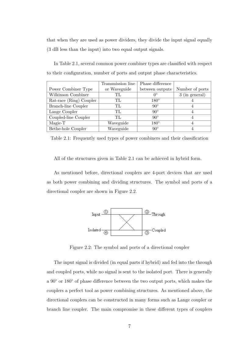
In Table 2.1, several common power combiner types are classified with respect
to their configuration, number of ports and output phase characteristics.
Transmission line Phase differencePower Combiner Type or Waveguide between outputs Number of ports
Wilkinson Combiner TL 0 3 (in general)
Rat-race (Ring) Coupler TL 180 4
Branch-line Coupler TL 90 4
Lange Coupler TL 90 4
Coupled-line Coupler TL 90 4
Magic-T Waveguide 180 4
Bethe-hole Coupler Waveguide 90 4
Table 2.1: Frequently used types of power combiners and their classification
All of the structures given in Table 2.1 can be achieved in hybrid form.
As mentioned before, directional couplers are 4-port devices that are used
as both power combining and dividing structures. The symbol and ports of a
directional coupler are shown in Figure 2.2.
Figure 2.2: The symbol and ports of a directional coupler
The input signal is divided (in equal parts if hybrid) and fed into the through
and coupled ports, while no signal is sent to the isolated port. There is generally
a 90 or 180 of phase difference between the two output ports, which makes the
couplers a perfect tool as power combining structures. As mentioned above, the
directional couplers can be constructed in many forms such as Lange coupler or
branch line coupler. The main compromise in these different types of couplers
7

is the ease of fabrication versus the bandwidth. For example, Lange couplers
are more difficult to design and build but have a higher bandwidth than the
branch line couplers. In addition to the corporate and spatial combiners, radial
combiners can also be used to combine power. These structures offer a high
bandwidth but they are harder to build.
Other than the power combiners just mentioned, structures which are used to
increase the gain can also be discussed. Among these configurations, cascading
several devices or using structrues like a traveling-wave (distributed) amplifier
are notable options. Traveling-wave structures employ active devices (transistors
or vacuum tubes) which are placed between two branches of gate (input) and
drain (output) transmission lines whose lengths are set such that the delays at
each device at the input and output lines are equal. The input signal propagates
through the input line and gets amplificated by each active device, resulting in a
signal traveling through the output line. The use of transmission line theory in
amplification leads to a gain which shows additive property (overall gain is the
sum of the gains from each active device) unlike the cascading of amplifiers where
the overall gain is the multiplication of the gains of separate devices. This may
seem as a compromise, but in return, the bandwidth can be increased without
limits in theory. In reality, what limit the bandwidth are the device parasitics.
A power combining structure where the quadrature directional couplers are
used is the balanced amplifier. The balanced amplifiers have two transmission
line branches employing power amplifiers in between. Hybrid couplers are placed
in the input and the output; where the input coupler divides the signal in two
equal parts and the output coupler is used to combine the amplified signals.
One advantage of using quadrature hybrid couplers is that the possible reflected
signals from the amplifiers combine destructively at the input port of the coupler
since there is a 90 of phase difference between two output ports and the reflected
signals which make a round-trip create a 180 of phase shift. The isolated port
8

of the coupler is terminated via a resistor, and the reflected signals which add in
phase are dissipated there. A similar task is also achieved by the output coupler,
and the amplified signals which are added in phase to make up the combined
signal are collected at the output.
2.2 Some Considerations in Power Combiners
While designing a power combiner, one has to consider the phase delay differences
that occur due to both the power combiner/divider structure and to the power
amplifiers used in the design. Many designs assume that the phase shifts in
each unit amplifier are equal. In practice, unit amplifiers cannot avoid having
variations in their output power and transmission phase even if the amplifiers
have the same design and are produced in the same lot [9, 10]. This problem
makes the phase balance in power combiners a key issue for high power combining
efficiencies.
In Figure 2.3, a typical N-way power combiner structure is shown. Li and Lo
are the power transmission factors. For example, for a 3-dB input loss, Li=0.5.
Figure 2.3: A typical power combiner structure
9

Assuming that all of the power amplifier outputs are in-phase and each of
them is equal to Poa, and the combiner is well-matched and balanced, the com-
bining efficiency ηc is given as [11]
ηc =PoNPoa
. (2.2)
Note that this ratio is equal to Lo, which implies that the combining efficiency
is only dependent on the output power transmission factor under the assumptions
made above.
DC power consumption is another important concept in power amplifiers.
Although it can be expressed in many ways, the most commonly used is the
power-added efficiency (PAE). It is given as [3]
PAE =Poa − PiaPdca
. (2.3)
The relationships between important design parameters like power, efficiency,
noise or graceful degradation in large power combiner systems are discussed in
detail by R.A.York in [11]. This work emphasizes that the ratio of overall PAE
of the general combiner system to the PAE of a single combiner is an impor-
tant indicator of how well several power amplifier outputs are combined without
degradation in a power combiner. If we call the PAE of an individual amplifier
as ηa, then PAE of the overall system, ηsys, can be written as
ηsys =Po − PiPdc
=Pi(LiGLo − 1)
NPdca=
(LiGLo − 1)
Li(G− 1)ηa. (2.4)
It is thus seen that in the limit of high gain, ηsys → ηaηc. Therefore, it can be
deduced that high gain can compensate for the effect of input losses in a power
combiner. Since the combining efficiency is defined solely by the output loss, ηsys
is limited only by the output loss in the condition of high gain.
The question of which power combining scheme is better to use is also another
important consideration. Unlike corporate combiners, the combining efficiency
10

of parallel combining schemes such as spatial combiners or radial combiners does
not change much with the number of devices combined. On the other hand, they
offer poorer combining efficiency than classical corporate combiners when small
numbers of power amplifiers are combined. Therefore, it is more advantageous to
use these schemes at large combining arrays. An ideal binary corporate network
has a total output loss of Lo = αS where α is the loss per stage and S is the
number of stages. If we call the constant output loss of a spatial combiner as So,
it is seen that after a specific number of amplifiers combined, the combining effi-
ciency of the spatial combiners start to surpass that of the corporate combiners.
This critical number of devices is given as [11]
Nc = 2So[dB]/α[dB]. (2.5)
A typical value of α for a Wilkinson divider at X-band is about 0.15 dB, while
So of a spatial power combiner is about 0.5 dB [11]. Using these numbers, it is
seen that at X-band, spatial power combiners are preferable to corporate power
combiners for N ≥ 10 number of devices combined. For N < 10, corporate
binary networks are favorable.
This analysis assumes that the unit amplifiers used in the combiner are iden-
tical and hence the amplifier outputs are in-phase and equal in magnitude. As
mentioned before, other than the output losses of the combiner, the phase imbal-
ances also play an important role in determining the combining efficiency. Thus
it is essential to take these imbalances into account for accurate results. In the
literature, this has been evaluated in several works in terms of its effects on the
graceful degradation or power combining efficiency characteristics of the power
combiner systems [12, 10, 13].
A simplified approach to power combiners in terms of current and voltage
is given by Tokumitsu et. al. in [9]. If Vkejθk voltage signals are added in a
combiner, where k = 1, 2, ..., N and at each branch a current of i1, i2, ..., iN flows
11

over a generator impedance of Zo, then at the output of the combiner, a total
current of i1 + i2 + ...+ iN flows through a load of Zo/N under the condition of
impedance matching. Then, at the kth branch, the relationship between voltage
and current can be written as:
Vkejθk = Zoik +
ZoN
(i1 + ...+ iN). (2.6)
The power dissipated in the load is obtained as
Po = |i1 + ...+ iN |2ZoN
(2.7)
=1
4NZo
∣∣∣∣∣N∑k=1
Vkejθk
∣∣∣∣∣2
(2.8)
The transition from Equation 2.7 to Equation 2.8 is given in Appendix A.
The total generated power is given as
PT =1
4Zo
N∑k=1
|Vkejθk |2. (2.9)
The combining efficency ηc is the ratio of the power dissipated in the load to
the total generated power and is equal to:
ηc =PoPT
x100(%) (2.10)
=
∣∣∣∑Nk=1 Vke
jθk
∣∣∣2N∑N
k=1 V2k
x100(%) (2.11)
This formula derived in [9] is useful to plot the combining efficiency versus
the variations at the phases or the power levels of the combined input signals.
This plot is seen below in Figure 2.4.
In order to produce the plot in Figure 2.4, it was assumed that the variations
in phase and power were uniformly distributed. For example, a phase variation of
20 means that each combined signal has a uniformly distributed random phase
ranging from -10 to 10 with respect to some arbitrary reference. The same is
12

Figure 2.4: Change of combining efficiency with input phase and power variations
also valid for the power plot. For example, for 4 dB variation, the amplitude
of each of the combined signals uniformly changes between 10(−4/20) = 0.631
and 1. The amplitudes of the combined signals were taken as equal for the plot
of phase variations, and the phases were taken as equal for the plot of power
variations. In order to get smooth-shaped curves, a combined signal number
N=10000 was assumed. As visible in the figure, in order to achieve a combining
efficiency better than 99%, a maximum phase variation of 15 or a maximum
power variation of 2.6 dB is necessary [9]. These numbers are also comparable
with the rated phase and amplitude imbalances of power combining structures,
which will cause extra variations in both the phases and the amplitudes. For
example, a typical specification of a 1 to 12.4 GHz 180 3 dB hybrid splitter
is given as ±0.8 dB amplitude imbalance and ±10 phase imbalance [5]. But
since these imbalances are inherent and cannot be improved unless the combiner
13

structure is changed, a high power combining efficiency can only be obtained by
setting the combined phases and amplitudes as close as possible. But as seen
in Figure 2.4, an 8 dB of maximum power difference which is a relatively high
value only leads to a 6% loss in combining efficiency, while an 80 of maximum
phase variation reduces the combining efficiency by 15%. This makes the phase
imbalance a much more important issue than the power imbalance in terms of
combining efficiency.
As mentioned above, the imbalance characteristics of the combining struc-
tures like splitters or couplers are also effective in determining the combining
efficiency. In the calculations above, these effects were not taken into considera-
tion and a perfect matching between the generators and the combining structure
was assumed. Another way of defining the combining efficiency is to write the ra-
tio of ηc to ηmax, where ηmax is the combining efficiency obtained when the added
signals are completely equal in magnitude and are in-phase. This way, the effect
of the combining structure losses is included in ηmax. Since ηc has information
about the phase and power mismatches, this ratio not only gives information
about the combiner losses, but also about the phase and amplitude mismatches
of the added signals. In order to obtain this ratio, a general expression for ηc can
be written in general form as [10]
Po = ηc
N∑k=1
Pav,k (2.12)
where Po is again the power at the output of the combiner and Pav,k is the
available power from each of the k combined signals. In order to relate ηc to ηmax,
another expression for Po in terms of ηmax is necessary. When the signals are not
equal in amplitude and phase, they are added vectorially so the summation in
Equation 2.12 can be written as [10, 14]
Po = ηmax1
N
( N∑k=1
√Pav,k cos θk
)2
+
(N∑k=1
√Pav,k sin θk
)2 . (2.13)
14
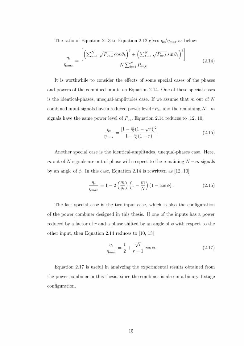
The ratio of Equation 2.13 to Equation 2.12 gives ηc/ηmax as below:
ηcηmax
=
[(∑Nk=1
√Pav,k cos θk
)2+(∑N
k=1
√Pav,k sin θk
)2]N∑N
k=1 Pav,k(2.14)
It is worthwhile to consider the effects of some special cases of the phases
and powers of the combined inputs on Equation 2.14. One of these special cases
is the identical-phases, unequal-amplitudes case. If we assume that m out of N
combined input signals have a reduced power level rPav and the remaining N−m
signals have the same power level of Pav, Equation 2.14 reduces to [12, 10]
ηcηmax
=[1− m
N(1−
√r)]2
1− mN
(1− r). (2.15)
Another special case is the identical-amplitudes, unequal-phases case. Here,
m out of N signals are out of phase with respect to the remaining N −m signals
by an angle of φ. In this case, Equation 2.14 is rewritten as [12, 10]
ηcηmax
= 1− 2(mN
)(1− m
N
)(1− cosφ) . (2.16)
The last special case is the two-input case, which is also the configuration
of the power combiner designed in this thesis. If one of the inputs has a power
reduced by a factor of r and a phase shifted by an angle of φ with respect to the
other input, then Equation 2.14 reduces to [10, 13]
ηcηmax
=1
2+
√r
r + 1cosφ. (2.17)
Equation 2.17 is useful in analyzing the experimental results obtained from
the power combiner in this thesis, since the combiner is also in a binary 1-stage
configuration.
15

Chapter 3
Design of Power Amplifiers
3.1 Project with Meteksan Savunma A.S.
The power amplifers were first designed as a part of a joint project with Metek-
san Savunma A.S. based on the idea that they could be used in the ongoing
projects of the company. The overall specifications set as the goals of the project
were outlined as follows: Two different designs would be made, the first of which
contained a fully distributed matching network, and the second of which con-
tained a matching network with lumped elements. The amplifiers would have a
frequency range of 2.8-3.2 GHz and produce a saturated output power of about
10 W (40 dBm) out of a 8-12 V DC supply, benefiting a GaAs device as the active
element. The amplifiers would have a gain of about 9-13 dB with a maximum
of 2 dB peak-to-peak flatness in the given bandwidth. The desired input return
loss, S11, was required to be below -10 dB. Both the lumped and the distributed
designs would be fabricated on 20-mil-thick Rogers 4003 substrate.
TGA2923-SG from Triquint was chosen as the active element. It is a par-
tially matched packaged amplifier with a center frequency of 3.5 GHz, providing
a saturated output power of 10 W at that frequency [15]. Although the device
16

is rated as partially matched for 3.5 GHz, the center frequency of our design is
3 GHz; therefore matching networks at the input and output along with DC-
biasing networks for the gate and the drain are necessary. The device technology
used in TGA2923-SG is Heterojunction Field Effect Transistor (HFET), or High
Electron Mobility Transistor (HEMT) which is a technology that has been sub-
ject to attention in recent years due to its good high-frequency and high-power
performance [1].
For the simulations, a new Touchstone file (.s2p format) was formed for
TGA2923-SG based on the measurements taken with the actual device, rather
than using the one provided by the company since the first design trials yielded
inaccurate results. The new Touchstone file was created for the bias conditions
of VD=8 V, VG=-1.4 V and ID=1200 mA and this file was used at all designs
with TGA2923-SG.
3.1.1 Agilent ADS and Momentum
While making the designs, Agilent ADS (Advanced Design System) was benefited
as a CAD tool. ADS has both a schematic simulator and an EM simulator called
Momentum. The schematic simulator makes use of the ADS or SPICE models of
the electrical components in the design while Momentum benefits the method of
moments technique to solve Maxwell’s electromagnetic equations. The microwave
mode or full-wave mode of Momentum uses full-wave Green functions which are
general frequency dependent Green functions that fully characterize the planar
structures embedded in a multilayered dielectric substrate without making any
simplification to the Maxwell equations [16].
Momentum also has an RF-mode or quasi-static mode that makes an ap-
proximation by assuming the Green functions frequency-independent in order
to reduce the simulation time, but in all the simulations performed during the
17

preparation of this thesis, microwave mode of Momentum was utilized. The
designs were made and optimized at the schematic simulator and were checked
by Momentum, and recursive changes were made between schematic and EM
simulators when necessary.
3.1.2 Distributed Design
Design of the amplifier with distributed components was based on a Touchstone
file which gives the s-parameters of the device for different frequencies at a par-
ticular bias point. By looking at S11 and S22, without any matching networks,
TGA2923-SG is observed to have an inductive reactance at both the input and
the output throughout the 2.8-3.2 GHz bandwidth. This is shown in Figure 3.1.
Figure 3.1: Input and output impedances of TGA2923-SG between 2-4 GHz
In order to match the device to 50 Ω which is the characteristic impedance
of the input line and also of all the measurement tools that are used, it is clear
that a negative reactance has to be introduced to the input. For the output,
the impedance seen by the transistor should be Ropt, which is the optimum
impedance that yields the maximum output power of a power amplifier. Hence,
the output matching network should transform the 50 Ω to Ropt. For the ideal
18

case, at the input, starting from the active device, matching can be achieved
most easily first by a relatively large series capacitor and then a relatively small
shunt capacitor. For a distributed matching network, these capacitances have
to be created with transmission lines. On the other hand, it is also important
to keep the bandwidth requirement in mind while doing the design. Therefore,
the matching networks get relatively complex to achieve the high bandwidth.
But ultimately, the main goal is to converge to 50 Ω by a group of distributed
elements that show capacitive characteristics.
Lumped elements can be realized by distributed components in a number of
ways. One of them is to change the thickness of the microstrip line. In 20-mil
thick Rogers 4003 substrate, 50 Ω corresponds to a line thickness of about 46
mils in microstip configuration. Lines that are thicker and thinner correspond to
lower and higher impedance lines respectively. A series high impedance trans-
mission line of a specific value roughly corresponds to a series inductor while a
series low impedance line corresponds to a shunt capacitor. Shunt transmission
lines can also be used. A short shunt transmission line with an open-circuit
termination means a shunt capacitor while a short shunt transmission line with
a short-circuit termination implies a shunt inductor. In the distributed design
matching network, only varying thicknesses and lengths of transmission lines
were benefited.
In Figures 3.2-3.7, the final form of the distributed design is shown. These
are screenshots from the ADS schematic window. In Figures 3.2 and 3.3, the
input and output matching networks can be seen respectively. The networks are
fully composed of microstrip transmission lines of different widths and lengths
which are optimized for the best S-parameters. The widths of the transmission
lines used in the distributed design are parametrized and their values can be seen
in the list named ‘VAR’ in Figure 3.2. It can be deduced from Figure 3.1 that
in the input matching, the most important component is the shunt capacitor
19

since it directly carries the input impedance of the device to the proximity of 50
Ω. Thus, as shown in Figures 3.2, several low impedance lines were used at the
input matching network.
Figure 3.2: Input matching network of the distributed design with TGA2923-SG
Figure 3.3: Output matching network of the distributed design with TGA2923-SG
The path that the input matching network transmission lines form on the
Smith chart at 3 GHz is shown in Figure 3.4. Starting from 0.194 + j0.5 point
which is the normalized input impedance of TGA2923-SG, the impedance of the
network converges to the vicinity of 50 Ω. This is also shown at the right of the
figure for the whole bandwidth. With this result, the input return loss can be
expected to be satisfying the asked conditions.
20

Figure 3.4: a) Input matching network displayed in the Smith chart for 3 GHz; b)The termination point of the input matching network for all frequencies withinthe bandwidth
For Class A operation, Ropt, the optimum impedance that allows the maxi-
mum output power is given by
Ropt =Vmax
Imax
=VDD
IRF
. (3.1)
The bias conditions of TGA2923-SG are VD=8 V and ID=1200 mA. For a
more realistic approach, the efffect of the knee voltage on the voltage swing
should also be considered, resulting in Ropt = 7 V / 1.2 A = 5.83 Ω. In Figure
3.5, it can be observed that the designed output matching network transforms
50 Ω to an impedance whose real part is about 25 Ω. This value is higher than
the Ropt value of Class A operation. Although the designed matching network
provides a good return loss, this variation from the optimum value means that
the maximum power performance of near 40 dBm may not be achieved. Actually,
the input and output matching networks function to shift the center frequency
of the TGA2923-SG to 3 GHz. As mentioned before, the transistor is normally
21

matched to 50 Ω with a bandwidth of 200 MHz at a center frequency which is
about 3.5 GHz [15]. This also creates a partial matching effect at 3 GHz, which is
the main reason why the distributed power amplifier design made in this thesis is
able to work with an impedance presented to its output higher than Ropt, at high
input levels, delivering a saturated power of about 38 dBm, as will be mentioned
later on.
Figure 3.5: a) Output matching network displayed in the Smith chart for 3 GHz;b) The impedance of the output matching network seen from the transistor side
The DC-bias networks for the input and output are shown in Figures 3.6 and
3.7 respectively. The bias networks also include distributed elements along with
surface-mount by-pass capacitors of 1 µF, 120 nF and 100 pF. The networks
were designed to present an open-circuit to the matching networks at 3 GHz,
thus not to disturb the RF characteristics. Shunt radial stubs were benefited to
increase the bandwidth of the DC-bias network, observable in Figures 3.6 and 3.7.
The radii and the angle of the shunt radial stubs were among the optimization
parameters. The width of the drain bias line was chosen thicker than that of
the gate bias line in order to have the lines withstand higher currents since the
22

Figure 3.6: Gate DC-bias network of the distributed design with TGA2923-SG
rated quiescent drain current is 1200 mA for TGA2923-SG. A resistor of 10 Ω
was included in the gate bias network to make the circuit stable at 3 GHz.
The S-parameter magnitude simulation results for the distributed design are
shown in Figure 3.8. As already mentioned, the simulations were performed in
both ADS Schematic Simulator and EM Simulator; and a comparison between
these two results is provided in Figure 3.8.
It is observed that S11 is less than -10 dB in the 2.8-3.2 GHz range in both
simulations. The gain, S21 is around 10 dB. The differences between EM and
schematic simulation results are due to different approaches to the same problem,
23

Figure 3.7: Drain DC-bias network of the distributed design with TGA2923-SG
24

Figure 3.8: S-parameters of the distributed design obtained via ADS Schematicand ADS Momentum (EM) simulations plotted together
but in terms of the reliability, EM simulation is preferable since it is the direct
simulation of the physical layout rather than the model. The simulation results
were satisfying in terms of attaining the goals set for the S-parameters, therefore
the development process went on with the fabrication of the amplifier. The
fabrication layout formed in Momentum and the fabricated amplifier with all the
components soldered are shown in Figure 3.9 and 3.10 respectively. As visible in
Figure 3.9, there are several vias in the ground plane pad on which the transistor
is placed. Thin wires are used to short this pad to the bottom ground plane of
the microstrip. The vias are also important in the process of transferring the
heat from the transistor to the bottom ground and the heat sink.
3.1.3 Measurement Results for the Distributed Design
The S-parameters and input-output power, efficiency, gain and intermodulation
characteristics of the distributed design with TGA2923-SG were measured by
25

Figure 3.9: Fabrication layout of the distributed PA design
Figure 3.10: The photograph of the fabricated distributed PA design
using the measurement tools in Meteksan Savunma. Measured S-parameters of
the design with a comparison with the EM simulation results are shown in Figure
3.11.
26

Figure 3.11: S-Parameters of the distributed PA: Measured vs. simulated
As mentioned before, the S-parameter measurements were taken at the bias
conditions of VD=8 V, VG=-1.4 V and ID=1200 mA. S11 satisfies the require-
ments in most of the bandwidth except after 3.15 GHz where it drops down to
about -5 dB; but S22 seems to be the limiting factor though not worse than a
rather acceptable level, which is better than -8 dB in the whole bandwidth. The
gain, S21 varies between 8.8 dB to 9.9 dB in 2.8 GHz-3.15 GHz range. After
3.15 GHz, it drops to about 8.2 dB. This value for gain is in agreement with the
rated gain values of TGA2923-SG, whose nominal gain is stated as 9 dB in the
datasheet. Measured S-parameters of the amplifier show a degree of consistency
with the simulations since the center frequency and the bandwidth goals are ob-
served as attained despite the differences in the magnitudes of the S-parameters.
The diagram of the experimental setup used for the power measurements is
given below in Figure 3.12 and the setup is shown in Figure 3.13.
27

Figure 3.12: Diagram of the experimental setup for power measurements
As can be seen in Figure 3.12, the input signal is produced by an RF signal
generator. Since the power levels provided by the signal generator is generally
rather low, in order to test the power amplifier at high power levels, it is necessary
to amplify this input signal to above 30 dBm. Therefore a driver amplifier by Cree
was benefited before the DUT. The driver amplifier consisted of a demonstration
board for CMPA2560025F, a Cree high-power GaN HEMT. This driver amplifier
could provide up to 44 dBm saturated power and 27 dB power gain at 3 GHz
[17]. Thus it is more than enough for the measurements as a driver amplifier.
SMA plug DC block capacitors were placed both before and after the driver
amplifier and the DUT for proper operation. SMA cables were used for making
the connections. Two 20 dB atteunators from Aeroflex/Weinschel were connected
after the DUT and the power levels were observed at the spectrum analyzer
from Rohde&Schwarz. Since the cables and DC blocks are not ideal, it is also
important to find their loss in order to correctly calculate the saturated power of
the DUT. For this reason, the whole system was tested bypassing the amplifiers
and was found to create a loss of 41.9 dB including the attenuators, meaning a loss
of 1.9 dB. Hence, all of the data that have resulted from the power measurements
were added 41.9 dB.
28

Figure 3.13: Photograph of the experimental setup for power measurements
Heatsinks were used at both the driver amplifier and the DUT. Heating is
an important issue for power transistors, degrading the performance seriously in
a rapid way when caution is not taken. Since the back side of the TGA2923-
SG, which is also the source terminal, has to be grounded and in the microstip
configuration only the lower conductor serves as ground (unlike some of the other
transmission types like coplanar waveguide), many vias of 0.4 mm diameter were
drilled on the top conductor where the transistor would be soldered, and thin
conducting wires were used to short the source of the transistor to the ground.
Same technique was also used to make the ground connections of the surface
mount (SMT) parts. Then the amplifier was located on a heat sink after putting
some thermal grease between the heatsink and the location where the transistor
would be placed. Thermal grease is a frequently used fluidic substance with high
thermal conductivity but also electrical nonconductivity that transfers the heat
directly from the active device to the sink.
As mentioned, it is important that the active devices stay below a certain tem-
perature limit for safe operation. TGA2923-SG datasheet gives the maximum
29

operating channel temperature and channel-to-backside of package thermal re-
sistance as 200C and 8C/W respectively under the bias conditions of VD=8 V
and ID=1.20 A [15]. For an ambient temperature of 25C and total DC power
consumption of about 10 W, the case-to-ambient thermal resistance is found as
(200− 25)C
10W− 8C/W = 9.5C/W. (3.2)
This is the maximum value of thermal resistance for the heat sink to be se-
lected. It should be noted that in this analysis, the case-to-heatsink and heatsink-
to-ambient transfer characteristics were not considered separately. This is be-
cause that the thermal resistance of the thermal grease which grants the heat
transfer between the case and the heatsink is very small (about 0.03 C/W) [18],
and can be neglected. One of the most frequently used heatsinks for cooling
of such a system is an aluminium flatback profile heatsink. One such example
is Aavid Thermalloy 60630, which is a flatback with gap profile heatsink with
dimensions of 99.1 x 32.5 mm. The rated thermal resistance for this model is
2.29 C/W [19], which is a much lower value than the number calculated above.
In the power measurements, a heatsink which is about twice the size of the given
example was used. In order to be completely safe, fans were also benefited for
cooling the driver amplifier and the DUT.
The change of output power with respect to the input power is plotted in
Figure 3.14. Nonlinear effects start to be observed after an input power level of
about 26 dBm, which corresponds to an output power level of 34.3 dBm. The
1-dB compression (P1dB) point is an important parameter for determining the
nonlinear characteristics of a power amplifier. The ideal behavior of the amplifier
which is characterized by a line is also plotted in Figure 3.14. By utilizing the
input-output power curve and this line, input and output 1-dB compression
points, which are named as P1dBin and P1dBout respectively can be determined.
P1dBin and P1dBout of the amplifier are found to be 28.9 dBm and 36.4 dBm
respectively from Figure 3.14.
30

Figure 3.14: Output power vs. the input power in distributed PA design
The nonlinear characteristics of the amplifier is also visible in the power gain
curve, which is plotted in Figure 3.15. Gain in the linear region seems to be
around 8.6 dB, and starts to deteriorate after a point, dropping down to around
5 dB at 33 dBm of input power in a nonlinear fashion.
Another important parameter in power amplifier design is efficiency.
Efficiency-linearity trade-off constitutes one of the main challenges in power am-
plifier design. Class A power amplifiers are the most linear but the least efficient
class of PA’s with a maximum 25% PAE since they conduct all the time. If an
inductor or a transformer is used to couple the load from the amplifier, theoret-
ical maximum efficiency can be increased up to 50% by making use of the back
(counter) electromotive force of the inductor. Class B type power amplifiers are
more efficient offering a maximum theoretical efficiency of 78.5% but less linear
since they conduct only at half of the cycle. This means that Class B power
amplifiers have a conduction angle of 180, where conduction angle is the angle
over one period for which the device remains conducting. Classes C, D, E and F
31

Figure 3.15: Power gain vs. the input power in distributed PA design
provide much increased efficiency (up to theoretical 100%) but they are highly
nonlinear. In order to achieve an amplifier with a good compromise between
efficiency, power and gain, generally class AB is used. As their name implies,
Class AB type amplifiers are a mixture of the Classes A and B, meaning that
their quiescent points are set such that they conduct between a half and a full
cycle, i.e., they have a conduction angle of between 180 and 360 degrees.
The distributed design was also based on Class AB configuration. In the
literature, Class AB amplifiers have been shown to produce the same amount
of fundamental RF output power (in fact a few tenths dB better) with Class A
PA’s with increased efficiency and relatively low harmonic content [20]. In the
ideal case, throughout the Class AB range, the largest harmonic other than the
fundamental is observed as the second. The third harmonic is less dominant while
the effect of the fourth and the fifth harmonics are nearly negligible. The effect
of the second harmonic is to reduce the dips of the fundamental sinewave and
32

sharpen the peaks. The main purpose of the reduction of the conduction angle is
to increase efficiency, and effects of this sort are tolerable in case the fundamental
power level does not decrease very much. It is understood from the proposed
use of the active device TGA2923-SG that it has been optimized for Class AB
operation. The quiescent drain current recommended in the datasheet is 1.20 A,
while the device can withstand currents up to 4 A. It is clear that the device
gives the best performance in the AB range. Therefore, the distributed design
has been based on the recommended bias points of VD=8 V and ID=1200 mA,
which corresponds to a gate voltage of VG=-1.4 V for the particular device used.
The value of the gate voltage that yields the given drain current level for the
given drain voltage value varies from device to device. The suitable gate voltage
values have been found to be ranging from -1.56 V to -0.93 V experimentally for
several devices.
The power added efficiency versus the input power plot is shown in Fig-
ure 3.16. This curve was obtained by applying Formula 3.1 and taking PDC as
1.2x8=9.6 W for all input drive levels. The maximum PAE level is found to be
close to 45% for an input power of about 32 dBm. Small signal efficiency is low
as expected. Because the quiescent point does not change with the variation of
the RF input power, for small AC signals, efficiency is expected to be low. Then
for increasing RF drive level, the efficiency is expected to exponentially increase
and when the gain starts to drop, it is expected to decrease after reaching a
maximum. The datasheet of TGA2923-SG also gives similar curves for efficiency
and again a maximum level of about 45% for several application circuits from
3.5 GHz to 3.7 GHz [15].
Stability is also another important concept for power amplifiers. When un-
stability starts to be observed, the amplifier starts to act as an oscillator. In
order to check whether a 2-port network is stable, a commonly used test is called
33

Figure 3.16: Power-added efficiency vs. the input power in distributed PA design
the K-B1 test. K and B1 factors of a 2-port network are defined as [6];
∆ = S11S22 − S12S21 (3.3)
K =1− |S11|2 − |S22|2 + |∆|2
2|S12S21|(3.4)
B1 = 1 + |S11|2 − |S22|2 − |∆|2 (3.5)
With these definitions, a 2-port network is unconditionally stable if and only
if the criteria below are satisfied:
K > 1 (3.6)
B1 > 0 (3.7)
K andB1 factors extracted from the measured S-parameters of the distributed
design are shown in Figures 3.17 and 3.18 respectively.
As can be seen in the plots, the conditions of 3.6 and 3.7 are satisfied for
the distributed PA design. In the given bandwidth, the K-factor does not drop
34

Figure 3.17: K-factor stability of the distributed PA
below 1 while the B1 factor also stays above 0. This ensures the stability of the
design. As mentioned before, a 10 Ω resistor was placed in the gate bias network
in order to get rid of possible oscillations. This was an experimentally determined
value. The detractive effect of this resistor on the gain is observed not to be very
significant since the gain values specified in the datasheet of TGA2923-SG were
achieved.
The third order intermodulation products of the amplifier were also measured
by another setup using two-tone measurement technique. Instead of one signal,
two sinusoidal signals of the same power level (-9 dBm) but of slightly different
frequencies (3 GHz and 2.998 GHz) produced by two different RF signal gen-
erators were combined via a Wilkinson power combiner and were fed into the
setup shown in Figure 3.12. Since the most dominant intermodulation products
are 2f1-f2 and 2f2-f1, two signals at frequencies 2.996 GHz and 3.002 GHz are ex-
pected to be observed most closely to the fundamentals f1 and f2 at the spectrum
35

Figure 3.18: B1-factor stability of the distributed PA
analyzer. The experimental results verify this expectation. Third order inter-
modulation products observed at the spectrum analyzer (whose power levels are
added by 41.9 dB of loss) are given in Table 3.1 below.
Frequency (GHz) Power (dBm)
2.996 -39.542.998 19.053.000 18.983.002 -39.69
Table 3.1: Power Levels of Fundamentals and Intermodulation Products Ob-served at the Output
Third-order intercept point, which is shown as IIP3 for input and OIP3 for
the output, is an important indicator of how well the undesired intermodulation
products are suppressed and how linear the amplifier is. The intercept point
due to second-order intermodulation products, OIP2, is not as much dominant
because its level is above OIP3 and it and can be much easier to filter the
second-order products since they are not as close as the third-order products to
the fundamentals. By drawing a linear input-output power plot as the one in
36

Figure 3.14, and also another plot with a slope which is three times the slope of
this line and intersecting these two lines at the IP3, one can calculate the OIP3.
After simple analytical geometry calculations, following equation gives OIP3 [6]
OIP3 = Pf1 +∆P
2(dBm) (3.8)
where Pf1 is the fundamental power at the output and ∆P is the difference be-
tween the fundamental power and the intermodulation product power in dB,
P2f1−f2 . By observing Table 3.1, we can take Pf1 as 19 dBm and P2f1−f2
as -39.6 dBm. Thus, ∆P=58.6 dB. By applying 3.8, OIP3 is calculated as
19+58.6/2=48.3 dBm. Generally, OIP3 is found to be about 10 dB higher than
the output 1-dB compression point, P1dBout for amplifiers. P1dBout of the dis-
tributed design had already been calculated as 36.4 dBm, which implies about
12 dB of difference between two points.
3.1.4 Lumped Design
Another design was also developed based on the specifications set by the project
with Meteksan Savunma which was a power amplifier containing lumped ele-
ments in the matching networks. The specifications were the same with the
distributed design. As pointed out before, the matching network has to include
a dominant shunt capacitor along with other elements. This time, in order to
realize those elements, surface mount capacitors along with shunt stubs with
short and open terminations were used instead of transmission lines with vary-
ing thicknesses. Using ideal lumped elements, the input matching network can
be constructed as shown in Figure 3.19.
In a realistic design, the connections are made with transmission lines. There-
fore, the lengths of the transmission lines should be optimized, too. In order to
obtain a high bandwidth with a realistic matching network, along with the two
series capacitors, a shunt short-circuited stub and several 50 Ω lines were also
37

Figure 3.19: a) An ideal 2-element input matching network; b) The S-parameterperformance of this network; c) The matching displayed on Smith Chart
benefited at the input and output. The ADS screenshots of the final form of the
matching networks are shown in Figures 3.20 and 3.21.
Figure 3.20: Input matching network of the lumped-element design withTGA2923-SG
In Figure 3.22, the input matching network of the lumped design is displayed
on the Smith chart. It can be observed that for the most of the bandwidth, the
impedance seen at the input side of the matching network approaches 50 Ω.
38

Figure 3.21: Output matching network of the lumped-element design withTGA2923-SG
Figure 3.22: a) Input matching network displayed in the Smith chart for 3 GHz;b) The termination point of the input matching network for all frequencies withinthe bandwidth
For the output matching network, the impedance seen from the transistor
side should again be close to Ropt for maximum output power. The designed
network carries the 50 Ω to an impedance whose real part is about 15 Ω, which
is a value higher than Ropt. Again it can be expected that the deviation from
Ropt at the output may reduce the saturation power of the amplifier. On the
other hand, the return loss and gain characteristics of the simulated design show
39

good characteristics. The output matching network elements displayed on Smith
Chart are shown in Figure 3.23.
Figure 3.23: a) Output matching network displayed in the Smith chart for 3 GHz;b) b) The impedance of the output matching network seen from the transistorside
Matching network designs using lumped elements are generally more com-
pact than the distributed designs and are easier to optimize after fabrication.
But it is more difficult to obtain an agreement between the simulation and ex-
perimental results. This is because the simulation models of the surface mount
lumped elements do not exactly mimic the real behavior of the components. It
is necessary to experimentally obtain the high frequency models of each lumped
component that would be used in the design, but since a discrete optimization
that changes the values of the components in a discrete way (unlike the one
for the distributed case which is continuous) is needed, it is difficult to obtain
models for a wide range of numerous surface mount components. The measured
S-parameters of the amplifier are plotted along with the Momentum simulation
results in Figure 3.24. This is in fact a post-fabrication optimized version of the
lumped design. The original design was found to have worse S-parameters, and
40

the surface mount capacitors were replaced with different values which finally
resulted in the S-parameter behavior shown in Figure 3.24. The final capacitor
values from left to right are 20 pF, 1 pF, 2.2 pF and 0.4 pF.
Figure 3.24: S-Parameters of the PA with lumped components: Measured vs.simulated
The s-parameters shown in Figure 3.24 are the best results among a set of
different combinations of surface mount capacitor values. Nevertheless, this best
combination still cannot satisfy the bandwidth requirement and S11 and S21 are
found to be several dB’s worse from the levels achieved by the distributed design.
On the other hand, the design displays a good symmetrical behavior, with the
s-parameters centered around 3 GHz. But S11 and S21 are only good at the center
frequency, and this is the best result among a several number of trials. It can be
deduced from these results that the difference between the ideal and non-ideal
performance of a matching network employing lumped elements is far greater
than that of a distributed matching network, which is closely related with the
imperfect modeling of the components, as mentioned before.
41

3.1.5 A Design with NPT1004
As an extra part of the project, an amplifier capable of producing a high output
power (which is about pulsed 30 W or higher) was also asked to be designed. In
order to supply such a high power, a GaN transistor, NPT1004 from Nitronex was
used. The frequency range was this time chosen as 3-3.5 GHz. The S-parameter
requirements were still valid. The amplifiers would be designed with respect to
8-mil Rogers 4003 substrate. A design was made based on these specifications,
but the measurements revealed that the center frequency of the design was about
2.95 GHz. This frequency shift can again be attributed to the inaccuracy of the
Touchstone files provided by the company. The design parameters and the layout
obtained in ADS are given in Figures 3.25 and 3.26 respectively.
Figure 3.25: Input & output matching and bias networks of the amplifier designwith NPT1004
A fully distributed network was designed for matching. To ensure stability,
3.9 Ω was placed in the input matching network. 100 pF surface-mount ca-
pacitors were placed at the input and output for DC blocking. This time for
AC-DC separation, RF choke inductors were employed at the gate and drain
bias networks. For the gate bias network, an inductor with model number of
42

Figure 3.26: Fabrication layout of the NPT1004
0603CS-15-NX-L was selected. This inductor is rated as having a 4 GHz self-
resonance frequency. Its DC resistance at 3 GHz is rated as 0.170 Ω. For the
drain bias network, an inductor that could stand high currents was necessary,
and for that reason a conical inductor from Coilcraft with high current specifica-
tions was used. The simulations and the measured S-parameters for the device
are shown in Figures 3.27 and 3.28 respectively. The bias conditions for the
measurements were VD=28 V and ID=350 mA.
As can be observed in Figure 3.27, both the schematic and Momentum simu-
lations yield similar s-parameter results, which are satisfying for the whole band-
width. But the measurement results show that the center frequency of the design
has shifted to 2.95 GHz. Due to the lack of a GHz pulsed driver system at that
time, the pulsed power measurements were skipped but a good pulsed power
performance can be expected from the amplifier at that shifted frequency range.
On the other hand, the amplifier was tested with very brief continuous RF drives
at 3 GHz, and it was observed to perform decently up to about 43.05 dBm (20.18
W) of output power. Since the device is optimized for pulsed performance, the
device was not tested with further drive levels. The measurement results are
shown in Table 3.2.
43

Figure 3.27: Schematic and EM simulation results of the amplifier design withNPT1004
Figure 3.28: S-parameter measurement results for the amplifier design withNPT1004 for VD=28 V and ID=350 mA
44

PIN (dBm) POUT (dBm)
7.8 15.617.8 25.622.8 30.527.8 35.432.6 40.336.0 43.05
Table 3.2: Output Power vs. Input Power for the design with NPT1004
3.2 Final Form of the Amplifiers
For the amplifiers that would be used in the power combiner, the distributed
design with TGA2923-SG was chosen and two new power amplifiers with the
same design were fabricated. This time the DC block capacitors were integrated
with the circuit and two 100 pF capacitors were placed at the proper places within
the input and output matching networks so that they could have minimum effect
on the s-parameters. An extra amplifier was also fabricated in case one of the
two available ones failed. These power amplifiers were named as ‘I’, ‘II’, and ‘III’
respectively. The photograph of these amplifiers placed on heatsinks is given in
Figure 3.29, while the magnitudes and phases of the S21’s of the amplifiers I and
II are plotted in Figure 3.30.
Figure 3.30 shows that the phases experienced through PA I and PA II are
not exactly the same, although these two amplifiers are basically the same design
formed by the same elements. The main source of difference between the gains
and the phases of these amplifiers can be assumed to be the the transistors.
Although they are of the same model number, they are not the same. It had
already been noted that the value of the gate voltage that yields the given drain
current level for a given drain voltage value varies from device to device. For the
bias conditions of VD=8 V and ID=1200 mA, VG corresponds to about -1.4 V
and -1.0 V respectively for the PA I and PA II, which is also a proof of difference
between the transistors. In Figure 3.30, it is visible that there is more than 40
45

Figure 3.29: Final form of the amplifiers available for use in power combiner
Figure 3.30: a) Magnitudes and b) Phases of the S21’s of PA I and PA II
of phase difference between the amplifiers. It shows that the phase shifters will
indeed be important to compensate for the phase imbalance between the arms
since these amplifiers would be used in a power combiner. The center frequency
46

of the new amplifiers also shows a shift, the best s-parameter characteristics are
observed at about 3.07 GHz. Since this frequency is within the predetermined
range of 2.8-3.2 GHz for many elements like Wilkinson power combiners or the
couplers of the phase shifters which are used in the power combiner system, it is
possible to test the power combiner at this frequency.
47

Chapter 4
Phase Shifters
4.1 Information on Phase Shifters
Phase shifters are blocks that can be used to change the phase characteristics of
an input voltage or current by using a control signal. There are several applica-
tions where the phase shifters are frequently used. An important example is the
phased-array antennas, where beam scanning is controlled by shifting the phase
[6]. The change of phase in a phase shifter can either be continuous or in discrete
steps. Both analog and digital phase shifters are available. Analog phase shifters
make use of either passive microwave elements like transmission lines or active
components like transistors. Digital phase shifters offer discrete phase steps with
respect to the state of the phase bits which also determine the resolution of the
shifter structure.
The working principles of analog phase shifters are diverse. An analog phase
shifter can be transmission or reflection type. As the name implies, the output
of a transmission type phase shifter is the signal that transmits through the 2-
port network, while the output of a reflection type phase shifter is the signal
that reflects back from the 2-port. Each group may have various configurations.
48
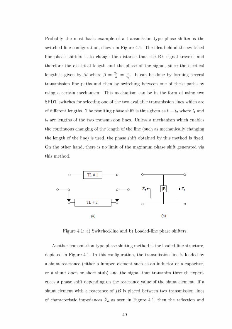
Probably the most basic example of a transmission type phase shifter is the
switched line configuration, shown in Figure 4.1. The idea behind the switched
line phase shifters is to change the distance that the RF signal travels, and
therefore the electrical length and the phase of the signal, since the electical
length is given by βl where β = 2πλ
= ωvp
. It can be done by forming several
transmission line paths and then by switching between one of these paths by
using a certain mechanism. This mechanism can be in the form of using two
SPDT switches for selecting one of the two available transmission lines which are
of different lengths. The resulting phase shift is thus given as l1− l2 where l1 and
l2 are lengths of the two transmission lines. Unless a mechanism which enables
the continuous changing of the length of the line (such as mechanically changing
the length of the line) is used, the phase shift obtained by this method is fixed.
On the other hand, there is no limit of the maximum phase shift generated via
this method.
Figure 4.1: a) Switched-line and b) Loaded-line phase shifters
Another transmission type phase shifting method is the loaded-line structure,
depicted in Figure 4.1. In this configuration, the transmission line is loaded by
a shunt reactance (either a lumped element such as an inductor or a capacitor,
or a shunt open or short stub) and the signal that transmits through experi-
ences a phase shift depending on the reactance value of the shunt element. If a
shunt element with a reactance of jB is placed between two transmission lines
of characteristic impedances Zo as seen in Figure 4.1, then the reflection and
49

transmission coefficients are given by
Γ =ZIN − ZoZIN + Zo
=1− yin1 + yin
(4.1)
T = 1 + Γ (4.2)
where yin is the normalized input admittance of the phase shifter and given by
(Yo + jB)/Yo = 1 + jb. Then, the reflection and transmission coefficients are
found as
Γ =−jb
2 + jb(4.3)
T =2
2 + jb. (4.4)
Here, the phase shift generated is equal to the phase of T, which is equal to
−tan−1(b/2) and the insertion loss of the phase shifter is equal to −10log10|T|2 =
10log10(1 + b2
4) in dB. Insertion loss is an important parameter that can be de-
fined as the attenuation ratio in a 2-port device. Although they can be used
as a variable continuous phase shifter by employing an element like a variable
capacitor, loaded-line phase shifters have important drawbacks. One of these
drawbacks is that the maximum phase shift obtained from these structures is
limited to 45. Also, in order to get a higher phase shift, one has to increase
b; which in turn results in an increase in the insertion loss [6]. A method that
can be used to overcome these drawbacks is to use two identical shunt elements
with a quarter wave transformer in between instead of only one shunt element.
This leads to better return loss characteristics by having the two reflected waves
cancel out by making them 180 out of phase.
The other phase shifter category is the reflection type phase shifters. Here,
the load that is placed at the end of the shifter is made switchable or continuously
variable so the reflection coefficient is modified in phase. Again there are several
implementation methods for reflection type phase shifters. One of them is to
change the length of the transmission line at the output by a switch. Another
one is to put a variable reactance at the output and change it by a control signal.
50

The latter method was benefited for the phase shifter used in our power
combiner. A 3-dB quadrature hybrid coupler (a branch line coupler) was used at
the input of the phase shifter, and the 2nd and 3rd ports, which are the through
and coupled ports, were terminated with varactors that can offer changeable
capacitance with changing DC bias. Since all arms of the branch line coupler
have a length of λ/4, the input signal fed from Port 1 splits into two 90 out
of phase but equal amplitude signals to Port 2 and Port 3. These two signals
reflect back from the terminations with a phase that is altered depending on the
value of the capacitance of the varactor. Since the same DC bias is used for
the identical varactors, it can be assumed that the additional phases that are
presented to these two signals are the same. Afterwards, as described in Chapter
2, the reflected signals combine destructively at the input port because now they
have 180 of phase difference due to the round trip, and they add up in Port 4
which is the output port since they are in-phase. The varactors used here should
be able to completely reflect the signals back without dissipating any power. In
order to achieve this, the varactors must have a reasonably high Q and thus, low
loss. The schematic of this phase shifter is given in Figure 4.2.
Figure 4.2: Reflection type phase shifter with hybrid coupler and varactors
4.2 The Phase Shifter with Varactors
As mentioned above, in order to be able to equal the phases of the signals at each
arm of the power combiner, a reflection type phase shifter employing varactors
51
at the output of a hybrid coupler was used in our work. In literature, this phase
shifting method has been shown to work well at different frequency bands with
high bandwidths [21, 22]. In this work, we have benefited two phase shifters at
the two branches of the power combiner. Here, the bandwidth is not critical
so a branch line coupler topology operating at the center frequency of 3 GHz
was preferred as a coupler. The coupler was designed by using Agilent ADS and
again tested with Momentum. The measured S-parameters of the branch line
coupler are given in Figure 4.3.
Figure 4.3: Measured s-parameters of the branch line coupler used in the phaseshifter
The S21 and S31 should be the same for the center frequency since they stand
for the amount of signal transmitting through the ports 2 and 3 respectively.
Here, at 3GHz, they are both close to -3 dB showing that the input signal is
divided into two equal parts at ports 2 and 3. The 4th port is the isolated port,
therefore ideally no signal is expected to go there. This is visible in Figure 4.3
since S41 is below -10 dB at the center frequency. The return losses are good and
52

they are below -10 dB for the whole band of 1 GHz and are below -20 dB at the
center frequency.
The varactors were chosen as MA46483 from MA-COM. These GaAs varac-
tors are able to offer high Q, which is critical in completely reflecting the incident
signals and thus decreasing the insertion loss of the phase shifter. The junction
capacitance of MA46483 changes between 1.3 pF and 12 pF for reverse tuning
voltages of 20 V and 2 V respectively. Since it is also important that the same
amount of phase should be added to the signals at ports 2 and 3 by the var-
actors, the reverse voltage-capacitance characteristics of the two varactors used
at a coupler should ideally be the same. In reality they should be as close as
possible to each other. For each MA46483 purchased, the measured junction
capacitance values versus a set of voltage levels are given. For example, for one
phase shifter, the two varactors used had the following capacitance values: The
first varactor is measured to have a Cj of 11.817 pF, 6.743 pF and 1.386 pF and
the second varactor is measured to have a Cj of 11.847 pF, 6.750 pF and 1.379
pF for voltage levels of 2 V, 4 V and 20 V respectively. These values are close
enough for the varactors to be used in the output of the same coupler. The Q’s
are given as greater than 1500 for both varactors. As given in Figure 4.2, DC
block capacitors and DC bias networks are necessary in order to separate the DC
and RF signal paths. Instead of using quarter-wave transformers, again the DC
bias networks which are used to present an open circuit for RF were optimized
with Agilent ADS for a better bandwidth as was done for the power amplifier
design. The photograph of the fabricated phase shifters along with the measured
s-parameters at a reverse voltage of 10 V are given in Figure 4.4.
As emphasized before, the insertion loss of a phase shifter is an important
parameter that shows how much signal is lost from the input to the output
port. From Figure 4.4, it is clear that the insertion loss is less than 1 dB. When
compared to the commercially available phase shifters and other phase shifters
53

Figure 4.4: a) The photograph of the phase shifters, b) S-parameters of one ofthe phase shifters
in the literature, it can be concluded that this value is quite satisfactory. For
example, the insertion loss of HMC928LP5E, a 2-4 GHz analog phase shifter
from Hittite Microwave Corporation, is given as 3.5 dB at the center frequency
while the insertion loss of P8P-48N-5, a digitally controlled 2-6 GHz phase shifter
from GT Microwave Inc., is given as 11 dB at maximum. The return losses are
also low, S11 and S22 are below -10 dB in the bandwidth of 400 MHz.
The phase shift generated by a varactor-based reflection type phase shifter
can be calculated by using the relationship between the capacitance and elec-
trical length, i.e., the phase. The input impedance of an open-circuited lossless
transmission line is given as [23]
Zi = − jZ0
tanβl. (4.5)
This is the reactance of a capacitance of tanβl/(ωZ0) farads. From this for-
mula, one can find out how many degrees of phase a capacitance value corre-
sponds to. If we replace βl with θ, then the phase corresponding to a capacitance
54

value can be calculated as
θ = 2tan−1(ωCZ0) (4.6)
where C is the capacitance. The factor 2 comes because the signal travels the
same distance twice. At another capacitance value, a different phase value will
be obtained. Therefore, the phase shift generated by this phase shifter is the
difference between these phase values corresponding to different capacitances.
By this method, a theoretical assumption of the phase shift that our phase shifter
can produce can be calculated by placing the values of 1.386 pF and 11.817 pF
for minimum and maximum capacitances. At 3 GHz, the theoretical maximum
phase shift ∆θ is thus found as 170 − 105 = 65. The actual measured phase
characteristics of the two phase shifters versus the reverse voltage are plotted
in Figure 4.5. Since the normally isolated 4th port acts as the output port in
reflection type phase shifters, the phase shown in Figure 4.5 is denoted as the
phase of S41.
Figure 4.5: Measured phase versus reverse voltage for the phase shifters
55

As seen in the plot, the maximum phase shifts obtained by the phase shifters
1 and 2 are equal to 5.50 − (−43.4) = 48.9 and −3.10 − (−53.0) = 49.9
respectively. These results are close to the theoretically predicted value of 65.
An offset of about 10 is observed between the phase shifters, which is related
with the differences in varactor capacitances. As mentioned before, these phase
shifters are placed at each branch of the power combiner. This means that a vari-
able phase shift of about 5.50− (−53.0) = 58.5 and −3.10− (−43.4) = 40.3
can be achieved for the 1st and 2nd arms of the power combiner respectively.
Therefore, the phase shifters are able to maintain a phase balance when an im-
balance within this range is in question. As plotted in Figure 3.30, the difference
between the phases of the two fabricated power amplifiers is close to 50, which
is a value that can be overcome by this system.
4.3 An Alternative Phase Shifter Design
During the studies of this thesis, an alternative microwave phase shifter has been
designed and the results were published in a letter at Microwave and Optical
Technology Letters [24]. A reflection-type shifter in nature, the structure makes
use of the flow of a conducting fluidic substance (in this case, mercury) in order
to change the length of the transmission lines placed at the end of a coupler.
The through and coupled ports of a wideband quadrature hybrid coupler are
connected to two transmission lines in coplanar waveguide configuration, which
are terminated in open circuit at first. On top of these two separate transmission
lines, microfluidic channels are formed as two slots in a layer of polydimethyl-
siloxane (PDMS). The same level of mercury is injected into the two containers
(in the form of two circular cavities in PDMS layer), and the position of the
mercury is changed by varying the pressure exerted on the containers by two
micropositioners. This way, these two channels can be short-circuited at any
desired point, and every position of mercury corresponds to a specific degree of
56

phase shift. The phase shift obtained by this microfluidic phase shifter is nearly
continuous and can be changed between 0 to 360 in a bandwidth of 2-6 GHz.
The phase shift characteristics obtained at 3 different frequencies are plotted ver-
sus the distance traveled by mercury in Figure 4.6. The main drawback of such
a system is the difficulty of its fabrication and setup. Also a high level of loss
was observed, but much of this can be attributed to the imperfect characteristics
of the wideband coupler that was built. Due to the level of insertion loss and
the difficulty of operation of this phase shifter, it has not been employed in the
power combiner system. The fabrication process and more details on the design
and the experimental results can be found in [24].
Figure 4.6: Measured phase shift versus the distance traveled by mercury
57

Chapter 5
Measurements on the Power
Combiner
5.1 Integration of the System Setup
The final step in the power combiner design was to put together all the compo-
nents and measure the effect of phase changes at the output power. The overall
power combiner testing setup diagram is given in Figure 5.1.
Figure 5.1: The overall power combiner test diagram
58

In order to obtain a sinusoidal RF signal, a voltage controlled oscillator was
benefited. ZX95-3100+, a linearly tuned, low phase-noise voltage controlled
oscillator from Mini Circuits was chosen. The frequency range provided is 2300-
3100 MHz and the DC voltage value corresponding to 3.07 GHz is about 8.9
V, with a power level of 8.8 dBm. This power level was increased by using an
RF driver amplifier, HP 8347A, which offered a leveled output power as high
as 22 dBm. As mentioned before, in order to separate the input into two equal
parts, a Wilkinson power divider was used. The same design was also employed
as a combiner at the output. In order to design the Wilkinson power divider,
again Agilent ADS and Momentum were utilized. The photograph and measured
s-parameters of the fabricated Wilkinson power divider is shown in Figure 5.2.
Figure 5.2: a) The photograph of Wilkinson power dividers, b) S-parameters ofWilkinson power divider #1
It can be observed that the Wilkinson divider operates at a wide frequency
range, offering an S21 and S31 which is around -3 dB throughout the whole
bandwidth. This means that the input signal is divided into two equal parts
and is sent through the ports 2 and 3 without much loss or imbalance of signal
divison. The return losses are also good, below -10 dB for nearly the whole
59

bandwidth. After the signal is splitted into two arms, it is fed through the phase
shifters and the power amplifiers at each arm. The power amplifiers are PA I and
II explained in Chapter 3 and the phase shifters are the reflection type shifters
using couplers terminated with varactors, as described in Chapter 4. The DC
control voltages which are in the 2-20V range are used to set the phase shift level
of each arm. As stated before, with this system, it is possible to obtain about
±50 phase shift.
The two amplified signals are then combined with a Wilkinson power com-
biner. They are then sent to a power detector after passing through a 40 dB
attenuator. The power detector is ZX47-40+ from Mini Circuits, a device that
can detect a 10-8000 MHz signal power level in the power range of -40 dBm to
20dBm. The detected power levels are converted to DC voltage values between
the terminals of a 1000 Ω resistor connected as a load to the output of ZX47-40+
and can easily be read with a multimeter. Although not as perfectly precise and
reliable as a spectrum analyzer, this power detector is much more practical to use
integrated in a system and is able to detect a wide range of power with quite good
accuracy. Of course, the detected power should be as harmonic-free as possible;
but, since the VCO has a very good harmonic performance (about -20 dBc), the
only possibly serious harmonic level is produced at the power amplifiers in the
system. But since the power amplifiers are operated in the linear region (leveled
output power from the driver amplifier was set as 20 dBm at maximum), and
P1dBin of the power amplifiers are about 29 dBm, a serious harmonic generation
should not be expected. Although the main function of a power combiner is to
provide a power level that each amplifier alone cannot offer, here the experiments
are made at a reduced power level. But the results obtained by these experi-
ments are also valid for the PA’s that are operated at their saturated output
power levels.
60

The experiment setup photograph is shown in Figure 5.3. Male-to-male and
male-to-female SMA cables from Emerson along with male-to-male adapters were
used for making the connections between the components. Several different volt-
ages are necessary for DC feed of power amplifiers, phase shifter control, VCO
tuning, power detector and fans that are used for cooling the amplifiers.
Figure 5.3: The photograph of the overall system setup
5.2 Measurement Results and Discussions
The power combiner system with a phase shifter was implemented as shown in
Figure 5.1. On this system, the effect of changing the phase of each arm of the
power combiner on the output power and combining efficiency can be observed.
The output power was measured for several phase combinations of the two phase
shifters, which are determined by DC voltages of values between 2 and 20 V. For
each combination, the phase difference between the arms and the corresponding
combining efficiency is calculated and plotted in Figures 5.4 and 5.5 for the
respective driving power levels of 4 dBm and 20 dBm obtained from HP 8347A.
It should be noted that the output power values in the figures are obtained when
the measured total loss due to the cables is added to the output power.
61

Figure 5.4: Change of the output power and combining efficiency versus thephase for 4 dBm drive level
Figure 5.5: Change of the output power and combining efficiency versus thephase for 20 dBm drive level
62

In the plots, the phase axis varies from -40 to 60. The adoption here is as
the following: Positive phases mean that the first arm is leading in phase and
negative phases mean that the second arm is leading in phase. For example, for
the obtained phases of -43 and -33 from the phase shifters, the phase of the
overall combiner is denoted as -10. These plots verify that the output power and
the efficiency of a power combiner indeed depend very much on the variations
in phase of each branch. A 3 and 4 dB variation in the output power is visible
in Figures 5.4 and 5.5 with changing the phase. It is clear that the maximum
output power and efficiency are obtained when the system has a phase of 60,
i.e. when the first phase shifter is set such that it gives an additional 60 of
phase to the first branch of the power combiner. This can be predicted from
the previously obtained Figure 3.30. In that plot, it is clear that phase of PA II
is about 45 ahead of PA I. Therefore, by setting the phase shifter before PA I
to give an additional amount close to this value, the phase balance between the
arms is achieved, leading to an increased output power and combining efficiency.
It is seen in Figures 5.4 and 5.5 that the maximum combining efficiency is
73% for an input power of 4 dBm and 76% for an input power of 20 dBm. The
results are about the same as expected since the output power in this situation is
about 7.5 dB above the drive levels for both 4 dBm and 20 dBm inputs from HP
8347A. This implies the gains of the power combiner are approximately equal
for both power levels since the measurements were made at the linear region
as emphasized before. These plots can also be compared to that in Figure 2.4.
Although the graph in Figure 2.4 is plotted for a combiner with N = 10000
amplifiers and although it shows the effects of phase and gain variation on the
combining efficiency separately, the general form of the curve is quite similar to
those in Figures 5.4 and 5.5. The rate of change of efficiency starts to slow with
gradually decreasing phase variation between the added signals in both figures.
If the additional phase for the first branch of the combiner was increased even
more, then the efficiency and the output power would naturally start to drop
63

again. It can be deduced that the maximum levels reached at these plots are the
maximum values for the efficiency and output power. Certainly, the difference
between the power levels of the added signals is also one of the factors that plays
an important role in diminishing the combining efficiency in our power combiner.
It is clear from Figure 3.30 that the gains of the two amplifiers are not exactly
the same at 3.07 GHz. A difference of more than 1 dB was also measured in the
power levels at the outputs of PA I and PA II for both the 4 dBm and 20 dBm
drive levels. This fact has also contributed to a lower combining efficiency.
It has been stated in Chapter 2 that ηc/ηmax formula gives important insight
about the effect of phase and power mismatches. For a binary power combiner
case, this formula is given in Equation 2.17. As mentioned before, without the
phase shifters, the phase difference between the two power amplifiers is about
45 while the difference between their gains, hence their output powers is about
1 dB. -1 dB corresponds to 0.794 in linear scale. Therefore, by putting 0.794 for
r and 45 for φ, we obtain
ηcηmax
=1
2+
√0.794
1 + 0.794cos 45 = 0.85. (5.1)
If we neglect the combining structure losses and impedance mismatches and
take ηmax as 1, then ηc is found as 85%. This means a 15% decline in ηc from the
maximum. If we inspect Figures 5.4 and 5.5, it is seen that the difference between
the ηc when the offset phases are not provided by the phase shifters (when the
system phase is equal to 0) and the maximum ηc is also close to this value. It
is equal to 73% − 56% = 17% in Figure 5.4 and 76% − 58% = 18% in Figure
5.5. As mentioned before, the maximum value of the efficiency is determined by
ηmax.
As mentioned previously, the measurements were taken at 4 dBm and 20 dBm
input levels. These points are within the linear region of the power amplifiers.
The phases of the amplifiers may deviate even further if the drive level approaches
64

the saturation point, especially because the transistors are not identical. In such
a case, the phase and power combining efficiency may not have a quasi-linear
fashion as in the curves of Figures 5.4 and combeff2. Even still, the phase shifters
are able to establish the phase balance between the arms by looking at the effect
of the phases on output power.
To sum up, controlling the phases in the fabricated binary power combiner
enables the combining efficiency to be increased about 15%, and the output power
is increased by more than 1 dB. The power amplifiers are normally expected to
have identical phase and gain characteristics since they are fabricated from the
same design by using the same transistor, but as shown, in practice they do not.
In real life applications, power combiners generally have higher number of stages.
Thus, if the phases are not correctly set at each binary branch and at each stage,
the combining losses can reach to significant levels.
65

Chapter 6
Conclusions
In this study, an S-band corporate binary power combiner comprising two power
amplifiers was designed and fabricated. In order to maintain a phase balance
between the two arms, two phase shifters were placed before the amplifiers. Since
the amplifiers used may have different phase characteristics in a power combiner,
phase shifters are necessary for a lower combining loss.
The power amplifiers were designed in a project with Meteksan Savunma.
CAD tools ADS and Momentum from Agilent were utilized while making the
designs. Both the frequency domain and time domain measurements of the
amplifiers were made and the distributed design was found to produce a saturated
output power of 38 dBm along with a PAE up to more than 40% at saturated
output power levels and a power gain close to 9 dB at linear power levels. Other
designs were also created with lumped elements, but the distributed design was
found to be superior in terms of bandwidth and s-parameters and it was chosen
to be used in the power combiner.
The phase shifters were designed based on reflection type phase shifting
method. For this purpose, a branch line coupler was used to have an input
and output signal. Two varactors were placed at the through and coupled ports
66

and they reflected back the incident signal with a phase changing with the reverse
DC bias applied on them. In order to have a very small insertion loss, it was es-
sential that the varactors could reflect back all of the signal without dissipating
any power. For this purpose, two high-Q varactors whose voltage-capacitance
characteristics were very similar were chosen for each phase shifter. The fabri-
cated phase shifters were found to be able to create a phase that could vary in
a range of 50. This value for each phase shifter is sufficient to compensate for
the phase imbalance created by the power amplifiers.
Finally, the power combiner system was formed by integrating all of the
separate components. Two Wilkinson couplers were fabricated to divide and
combine the signals at the input and output. The change of the output power and
combining efficiency were examined with changing the phases of each branch of
power combiner. In the 60+40 = 100 phase shifting range, it was observed that
ηc and the output power were indeed affected negatively by the phase difference
at each arm. A maximum ηc of 76% was obtained for 20 dBm of input power
to the combiner. This value was found as 58% in case the phases were not
controlled. The power loss and hence the reduction in the combining efficiency
would be even more alarming at higher stage power combiners.
Although this power combiner has been designed and fabricated comprising
of several discrete elements, all of these elements can be integrated into one single
structure, which may make the system more compact and convenient. The sys-
tem can also be operated at the saturated output power or at a higher frequency.
The combining scheme can also be changed into e.g. a spatial configuration. But
the phase and gain dependency of the combiner will not change and will bear the
characteristics shown by the system in this thesis. As mentioned in Chapter 2,
corporate power combiners are easier to design and they have a higher combining
efficiency for relatively small number of combined amplifiers. Hence, they stand
as an almost inevitable solution at microwave power systems.
67

A future enhancement in such a combiner system may be to automatically
control the additional phases produced by the phase shifter. This can be achieved
by processing the DC voltages produced by the power combiner and selecting the
phase levels for both phase shifters where the maximum power is observed. The
settling time of the whole system which is strongly dependent on the heating
of power amplifiers and the power detector should also be taken into account
for a better result. By automating the power combiner, it will be possible to
obtain the highest combining efficiency without controlling the phase shifters
manually. This automation process is especially important for higher stage power
combiners, where it would be much more difficult to manually control a high
number of phase shifting structures.
68

APPENDIX A
Derivation of Equation 2.8 from
Equation 2.7
If we write the generator voltages at each branch seperately we get;
V1ejθ1 = Zoi1 +
ZoN
(i1 + ...+ iN)
...
VNejθN = ZoiN +
ZoN
(i1 + ...+ iN)
When these terms are summed at both sides, we get:
N∑k=1
Vkejθk = Zo
N∑k=1
ik +ZoNN
N∑k=1
ik
Then,
i1 + ...+ iN =
∑Nk=1 Vke
jθk
2Zo
Therefore, Po of Equation 2.7 can be rewritten as
Po = |i1 + ...+ iN |2ZoN
=1
4NZo
∣∣∣∣∣N∑k=1
Vkejθk
∣∣∣∣∣2
which is Equation 2.8.
69

Bibliography
[1] Y.-F. Wu, “30-w/mm gan hemts by field plate optimization,” IEEE
ELECTR DEVICE L, vol. 25, no. 3, pp. 117–119, 2004.
[2] K. Chu, P. Chao, M. Pizzella, R. Actis, D. Meharry, K. Nichols, R. Vaudo,
X. Xu, J. Flynn, J. Dion, and G. Brandes, “9.4-w/mm power density algan-
gan hemts on free-standing gan substrates,” IEEE ELECTR DEVICE L,
vol. 25, no. 9, pp. 596–598, 2004.
[3] R. Gilmore and L. Besser, Practical RF Circuit Design for Modern Wireless
Systems, Volume II. Norwood, MA, USA: Artech House, 2003.
[4] N. Cheng, A.Alexanian, M.G.Case, D.B.Rensch, and R. York, “40-w cw
broad-band spatial power combiner using dense finline arrays,” IEEE T
MICROW THEORY, vol. 47, no. 7, pp. 1070–1076, 1999.
[5] D. Bockelman and W. Eisenstadt, “Combined differential and common-
mode analysis of power splitter and combiners,” IEEE T MICROW THE-
ORY, vol. 47, no. 7, pp. 1077–1082, 1999.
[6] M. M. Radmanesh, Radio Frequency and Microwave Electronics. Upper
Saddle River, NJ 07458, USA: Prentice Hall, 2001.
[7] N. Cheng, P. Jia, D. Rensch, and R. York, “A 120-w x-band spatially com-
bined solid-state amplifier,” IEEE T MICROW THEORY, vol. 47, no. 12,
pp. 2557–2561, 1999.
70

[8] J. Jeong, Y. Kwon, S. Lee, C. Cheon, and E. Sovero, “1.6- and 3.3-w power-
amplifier modules at 24 ghz using waveguide-based power-combining struc-
tures,” IEEE T MICROW THEORY, vol. 48, no. 12, pp. 2700–2708, 2000.
[9] Y. Tokumitsu and T. Saito and N. Okubo and Y. Kaneko, “A 6-GHz 80-W
GaAs FET Amplifier with a TM-Mode Cavity Power Combiner,” IEEE T
MICROW THEORY, vol. 32, no. 3, pp. 301–308, 1984.
[10] M. Gupta, “Degradation of power combining efficiency due to variabil-
ity among signal sources,” IEEE T MICROW THEORY, vol. 40, no. 5,
pp. 1031–1034, 1992.
[11] R. York, “Some considerations for optimal efficiency and low noise in large
power combiners,” IEEE T MICROW THEORY, vol. 49, no. 8, pp. 1477–
1482, 2001.
[12] R. Ernst, R. Camisa, and A. Presser, “Graceful degradation properties
of matched n-port power amplifier combiners,” in IEEE MTT-S Int. Mi-
crowave Symp. Dig., June 1977.
[13] J. Nevarez and G. Herskowitz, “Output power and loss analysis of 2n
injection-locked oscillators combined through an ideal and symmetric hybrid
combiner,” IEEE T MICROW THEORY, vol. 17, no. 1, pp. 2–10, 1969.
[14] K. Lee, “A 25 kw solid state transmitter for l-band radars,” in IEEE MTT-S
Int. Microwave Symp. Dig., May 1979.
[15] TGA2923-SG Datasheet. 2009. URL: http://www.triquint.
com/prodserv/more_info/download.aspx?file=/docs/t/TGA2923/
TGA2923-SG.pdf.
[16] Theory of Operation for Momentum. 2008. URL: http://cp.
literature.agilent.com/litweb/pdf/ads2008/mom/ads2008/Theory_
of_Operation_for_Momentum.html.
71

[17] CMPA2560025F Datasheet. 2011. URL: http://www.cree.com/products/
pdf/CMPA2560025F.pdf.
[18] Scythe Thermal Grease Datasheet. 2011. URL: http://www.scythe-eu.
com/en/products/pc-accessory/thermal-grease.html.
[19] Aavid Thermalloy Heatsink 60630 Datasheet. 2011. URL:
http://www.aavidthermalloy.com/cgi-bin/exdisp.pl?Pnum=
60630&LengthUnits=in&ExLength=3&airflow=57.2.
[20] S. C. Cripps, RF Power Amplifiers for Wireless Communications. Norwood,
MA, USA: Artech House, 2006.
[21] T. Morawski, J. Zborowska, and P. Miazga, “Multi-octave phase modula-
tors,” in IEEE MTT-S Int. Microwave Symp. Dig., 1984.
[22] D.M. Krafcsik and S.A. Imhoff and D.E. Dawson and A.L. Conti, “A Dual-
Varactor Analog Phase Shifter Operating at 6 to 18 GHz,” IEEE T MI-
CROW THEORY, vol. 36, no. 12, pp. 1938–1941, 1988.
[23] D. K. Cheng, Field and Wave Electromagnetics. Boston, MA, USA: Addison
Wesley, 1989.
[24] B. Ozbey, S. Ozturk, and O. Aktas, “Design of a high-resolution microfluidic
microwave mems phase shifter,” MICROW OPT TECHN LET, vol. 53,
no. 8, pp. 1902–1905, 2011.
72