design of an 8192-point sequential i/o fft chip - iaeng · design of an 8192-point sequential i/o...
TRANSCRIPT

Design of an 8192-point Sequential I/O FFT ChipYun-Nan Chang, Member, IEEE
Abstract—This paper presents an efficient VLSI design of 8k-point pipeline fast Fourier transform (FFT) processor capableof producing the sequential order output. The proposed FFTarchitecture is derived based on the modified delay feed-forwarddata commutator, and processes the internal dual data streamsin the real and imaginary alternate approach. Compared withthe general pipeline FFT designs, ours can achieve full butterflyhardware efficiency such that the required number of adderscan be reduced by a half. In order to generate the sequentialoutput order sequence, this paper also proposes an efficientreorder buffer design which can be used to replace the laststage’s commutator module for the saving of internal buffer. TheFFT decomposition method for the proposed design is based ona new radix-22 × 22 FFT algorithm such that only two and ahalf general complex-number multipliers are used. Finally, byproper data partition and allocation, the data storage requiredfor data commutators and the output reorder buffer canboth be efficiently realized by multi-bank single-port memorymodules. The proposed FFT processor has been implementedand fabricated by 0.18µm CMOS process technology. Thecore size is about 8.74mm2. This chip is suitable for digitalvideo broadcasting (DVB) applications not only because itcan perform the sequential input/output order 8k FFT, butit also consumes low power. To satisfy the DVB throughputrequirement, this chip can run under the clock rate of 8MHzand the supply voltage of 1.33V, and only dissipates 20.6 mW.
Index Terms—FFT, DVB.
I. INTRODUCTION
IN recent years, due to the widespread use of the orthog-onal frequency division multiplexing (OFDM) commu-
nication systems, how to design an efficient dedicated FFTcircuit especially for the emerging OFDM applications is avery important issue. Many FFT designs have been proposedin the last decade [1]-[14], which can be categorized intonon-pipeline and pipeline architectures. The non-pipelineFFT designs [1]-[3] utilize some centralized multiplier andbutterfly arithmetic units to iteratively perform one stage ofthe computation after the other, and the intermediate resultsare stored in the central memory unit. This approach canachieve compact design but since the level of parallelismof this approach is restricted such that it is not suitablefor high-throughput applications. On the other hand, thepipeline FFT processors [4]-[14] allocate dedicated data-pathfor each FFT stage such that it can achieve better throughput,and particularly suitable for the processing of continuousstreaming input data.
The pipeline FFT designs can be further divided into twodifferent classes. The first class is based on the so-calledmulti-path delay feed-forward (MDF) data commutator [4]-[8] which suffers both low hardware utilization and highstorage space unless parallel input data streams are available.The other class of FFT designs is called single-delay feed-back (SDF) FFT [9]-[14] which requires less internal buffer
Manuscript received July 23, 2012; revised August 15, 2012.Y.-N. Chang is with the Department of Computer Science and Engineer-
ing, National Sun Yat-sen University, Kaohsiung, 80424, Taiwan.
by circulating partial computed results back to the originalstage to reuse the buffer space. They can also fully utilizethe multiplier units although the utilization of their adderunits that can be achieved is at most 50%. In addition tothe data commutator style, the FFT algorithm which mostof the early FFT designs adopt is based on the conventionalradix-2 FFT algorithm. In order to reduce the silicon costfor the realization of the twiddle factor multiplication in FFTalgorithm, several modified FFT algorithms including radix-4[6],[9], radix-8, radix-22[10], and radix-23 [11] are proposed.These modified algorithms explore those trivial factors in theFFT algorithm such that their multiplications can be realizedby dedicated constant multipliers instead of the generalones. In [15], a decimated dual-path delay fed-forward datacommutator unit has been proposed. Combined with the newre-order buffer design, the resulted FFT architecture cannotonly achieve fully butterfly unit utilization, but also supportthe normal input-output data order.
This paper presents an efficient implementation of a 8k-point FFT processor based on [15]. In addition, a newradix-22 × 22 FFT algorithm is also proposed to reduce thenumber of general multipliers required. The remainder of thispaper is organized as follows. Section II first presents theoverall architecture of the proposed FFT design. In SectionIII, the detailed implementation of each FFT sub-moduleis addressed. Section IV presents the implementation andcomparison results. Finally, some conclusion is given inSection V.
II. THE PROPOSED 8K-POINT FFT ARCHITECTURE
One of the main drawbacks of pipeline FFT designs com-pared with the non-pipeline is the low hardware utilizationof the butterfly units. For the 8k-point pipeline FFT design,it will require 13 butterfly stages based on any radix-2n
decomposition. Therefore, it will require 52 real-numberadders which represent a big portion of the entire FFT circuit.In order to reduce the adder cost, a new MDF design shownin Fig. 1 has been proposed [15]. Here the incoming data(dj) are first divided into real (drj ) and imaginary (dij) parts.Then they pass through two data commutator (DC) stagesto form dual data streams which consist of even-index datafollowed by odd-index data. The real and imaginary partsof data are present in the stream in the alternate order. Theremaining part of the FFT circuit is similar to the MDCFFT design with the exception that the data commutator andthe arithmetic units will operate the real and imaginary dataalternately. The function of data commutator, as shown inFig. 2 is used to permute the data sequence in order to befit for different stages of butterfly operation.
In Fig. 1, two twiddle factor multipliers are insertedbetween every two radix-2 stages; however, the actual imple-mentation of these multipliers may be able to be simplifieddepending on what factors they involve. Furthermore, what
Proceedings of the World Congress on Engineering and Computer Science 2012 Vol II WCECS 2012, October 24-26, 2012, San Francisco, USA
ISBN: 978-988-19252-4-4 ISSN: 2078-0958 (Print); ISSN: 2078-0966 (Online)
WCECS 2012

DC
L=N/4
1st stage logN stagelogN-1 stage
BFU
DC
L=1
BFUoutput
reorder
buffer
BFU↓2D
↓2
Fig. 1. The block diagram of the proposed pipeline FFT design whichgenerates the normal order output sequence.
Dual-port
Feedforward
Data
Commutator
Length (L) = D
01112 aaaaa DDD LL −−
01112 bbbbb DDD LL −−
012101 aaaabb DD LL −−
DDDDD aaabb 11212 +−− LL
Fig. 2. The function of the data commutator (DC) with a depth of L.
twiddle factors are involved for each stage depends on thedecomposition order applied to the DFT computation. Forexample, if the traditional decimation-in-frequency radix-2FFT decomposition is applied for the 8k-point FFT, almostevery stage requires general factor multipliers. The onlyexception will be the last several radix-2 stages which involvethe multiplication of only few simple factors which can berealized by some dedicated constant multipliers. In order toreduce the multiplication strength, the trivial factors shouldbe gathered to the same stages such that they can be realizedby some dedicated constant multipliers. In the past, the ideaof so-called radix-2n FFT has been widely adopted in thepast. In this paper, an extended method called radix-22 × 22
FFT is proposed for the implementation of 8k-point FFT.Fig. 3 shows the data flow diagram of the simplified DFTafter one stage of decomposition assuming N equals N1×N2.
N1
DFT
0NW
2Nx0x
0NW
22Nx
21 )1( NNx −
0NW
0NW
N1
DFT
1NW
12 +Nx1x
0NW
12 2 +Nx
1)1( 21 +− NNx11−N
NW
2NW
N1
DFT
)1( 2 −NNW
12 2 −Nx12 −Nx
0NW
13 2 +Nx
121 −NNx)1)(1( 21 −− NN
NW
)1(2 2 −NNW
N2
DFT
N2
DFT
N2
DFT
N1-point DFT N2-point DFTtranspositionfactor
multiplication
Fig. 3. The flow diagram of N-point DFT transformation after one-stageof decomposition asssuming N equals N1 ×N2.
A 8k pipeline FFT architecture can be divided into 13stages. The detailed decomposition order for 8k-point FFTbased on the proposed radix-22×22 FFT approach is shownin Table I where each decomposition step is represented by
three parameter N , N1 and N2 according to Fig. 3. Thefirst level of decomposition is to recursively decompose theoriginal DFT algorithm based on the function of 16-pointDFT. After the first level, the function of each 16-pointDFT will be further decomposed based on the 4-point DFT.Finally each of 4-point DFT computation is decomposedinto two 2-point DFT operations which is equal to the basicbutterfly function. Fig. 4 shows the block diagram of theresulted 8k-point pipeline FFT architecture. There are fourtypes of multipliers being used in Fig. 4. The blocks labeledm-I and m-II denote two different general complex-numbermultipliers. The multiplier type m-IV involves the factors 1,−1, j and −j such that it can be efficiently realized by simplemultiplexer circuits. The multiplier type m-III involves thefactors Wn
16, and can be realized by dedicated constantmultipliers built by about 16 adders. The proposed radix-22 × 22 FFT is superior to the radix-24 FFT [12] becausethe number of the constant multipliers can be reduced. Forexample, for 8k-point DFT, the radix-24 FFT requires sixdedicated W 2
16 multipliers while the radix-22 × 22 FFT onlyneeds three.
TABLE IPROPOSED DECOMPOSITION ORDER FOR 8K-POINT FFT.
Level Level-1 Level-2 Level-3Step N N1 N2 N N1 N2 N N1 N2
Step 1 8k 2 4k 16 4 4 4 2 2Step 2 4k 16 512Step 3 512 16 16
DC
L=4k
BFU m
II
1st stage
DC
L=2k
BFU
2nd stage
m
IVDC
L=1k
BFU
3rd stage
m
IIIDC
L=512
BFU
4th stage
m
IVDC
L=256
BFU m
I
5th stage
DC
L=128
BFU
6th stage
m
IVDC
L=64
BFU
7th stage
m
IIIDC
L=32
BFU
8th stage
m
IVDC
L=16
BFU m
I
9th stage
DC
L=8
BFU
10th stage
m
IVDC
L=4
BFU
11th stage
m
IIIDC
L=2
BFU
12th stage
m
IV
13th stage
output
reorder
buffer
BFU
iiiddd 012L
rrrddd 012L
012 dddL
riridddd 0022L
DC
L=1
riridddd 1133L
rirririrdddddddd 00240944094113 LL
rirririrdddddddd 40964096409881908190113 LL
Fig. 4. The overall block diagram of the proposed 8k-point FFT architec-ture.
In the first level decomposition of 8k-point DFT, since thevalue of 8k is not the power of 16, we have to decomposeit to the 4k-point DFT first by choosing either N1 or N2 to2. Here we prefer the former choice due to the followingreasons. First, the location of the general multipliers (stage1, 5, and 9 for 8k-point FFT) will be closer to the inputside compared with the other approach (stage 4, 8 and 12).Therefore, the cost of multipliers can be reduced since theword-length requirement for the stages closer to the inputside will be generally shorter. The other reason is that for theresulted FFT flow chart, half of the first stage of butterfly unitoutputs are multiplied by trivial factor W 0
16 which is equal
Proceedings of the World Congress on Engineering and Computer Science 2012 Vol II WCECS 2012, October 24-26, 2012, San Francisco, USA
ISBN: 978-988-19252-4-4 ISSN: 2078-0958 (Print); ISSN: 2078-0966 (Online)
WCECS 2012
to one. Based on this feature, the first stage multiplier can befurther simplified as discussed in the following subsections.
III. DETAILED FFT IMPLEMENTATION
In the following, the implementation of each moduleshown in Fig. 4 is discussed in details.
A. The arithmetic units
There are three general complex-number multipliers re-quired for 8k-point FFT architecture shown in Fig. 4. Thesecond and third multipliers are used to multiply two butterflyoperation results with associated twiddle factors in twocycles. Therefore, these type m-I multipliers blocks can berealized by one single complex-number multiplier to provideone factor multiplication each cycle. The details circuit isshown in Fig. 5(a) where the complex-number multiplieris implemented by three real-number multipliers with someextra adders based on
(Wr + jWi)× (ir + jii)= (Wrir −Wiii) + j(Wrii +Wiir)= [(Wr −Wi)× ir + (ir − ii)×Wi]
+j[(Wr +Wi)× ii + (ir − ii)×Wi]
. (1)
The other type of multiplier m-II shown in Fig. 4 can berealized even more simplified since one of the two outputsof the first stage butterfly unit is multiplied by the unity.Therefore, the multiplication of the other output can berealized by two real-number multipliers in time-multiplexingway as shown in Fig. 5(b).
Twiddle
Factor
ROM
rW
iW
ra
rb
ia
ib
ro
io
ri
ii
(a)
Twiddle
Factor
ROM
+/-
rW
iW
rb
ib
(b)
Fig. 5. The detailed circuit diagram of the multiplication unit used in theproposed FFT design: (a) type m-I multiplier, and (b) type m-II multiplier.
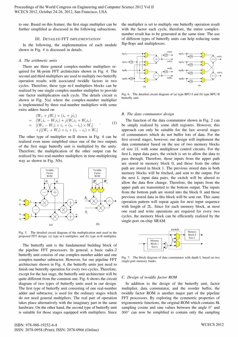
The butterfly unit is the fundamental building block ofthe pipeline FFT processors. In general, a basic radix-2butterfly unit consists of one complex-number adder and onecomplex-number subtractor. However, for our pipeline FFTarchitecture shown in Fig. 4, the butterfly units just need tofinish one butterfly operation for every two cycles. Therefore,except for the last stage, the butterfly unit architecture will bequite different from the common one. Fig. 6 shows the circuitdiagram of two types of butterfly units used in our design.The first type of butterfly unit consisting of one real-numberadder and subtractor, is used for the ordinary stages whichdo not need general multipliers. The real part of operationtakes place alternatively with the imaginary part in the samehardware. On the other hand, the second type of butterfly unitis suitable for those stages equipped with multipliers. Since
the multiplier is set to multiply one butterfly operation resultwith the factor each cycle, therefore, the entire complex-number result has to be generated at the same time. The useof different types of butterfly units can help reducing someflip-flops and multiplexors.
D
inpAr
inpAi
inpBr
DinpBi
D
D
outAr
outAi
outBr
outBi
(a)
inpAr
inpAi
inpBr
D
inpBi
outAr
outAi
D
+/-
+/-
D
D
(b)
Fig. 6. The detailed circuit diagram of (a) type BFU-I and (b) type BFU-IIbutterfly unit.
B. The data commutator design
The function of the data commutator shown in Fig. 2 canbe simply realized by some shift registers. However, thisapproach can only be suitable for the last several stagesof commutators which do not buffer lots of data. For thefirst several stages, however, our design will implement thedata commutator based on the use of two memory blocksof size 2L with some multiplexor control circuits. For thefirst L input data pairs, the switch is set to allow the data topass through. Therefore, those inputs from the upper pathare stored in memory block 0, and those from the otherpath are stored in block 1. The previous stored data in bothmemory blocks will be fetched, and sent to the output. Forthe next L input data pairs, the switch will be altered toallow the data flow change. Therefore, the inputs from theupper path are transmitted to the bottom output. The inputsfrom the bottom path are stored into the block 0. and thoseprevious stored data in this block will be sent out. This sameoperation pattern will repeat again for next input sequencewith length of 2L. Since for each memory block, at mostone read and write operations are required for every twocycles, the memory block can be efficiently realized by thesingle-port on-chip SRAM.
Memory
Block 1
Size L
switchMemory
Block 0
Size L
Fig. 7. The block diagram of data commutator with depth L based on twosingle-port memory banks.
C. Design of twiddle factor ROM
In addition to the design of the butterfly unit, factormultiplier, data commutator, and the reorder buffer, thetwiddle factor ROM is another major part of the pipelineFFT processors. By exploring the symmetric properties oftrigonometric functions, the original ROM which contains 8ksampling cosine and sine values between the angle 0◦ and360◦ can now be simplified to contain only the sampling
Proceedings of the World Congress on Engineering and Computer Science 2012 Vol II WCECS 2012, October 24-26, 2012, San Francisco, USA
ISBN: 978-988-19252-4-4 ISSN: 2078-0958 (Print); ISSN: 2078-0966 (Online)
WCECS 2012

values between 0◦ and 45◦. This reduction ratio of ROM isup to 1
8 with only slight overhead of three adders and severalmultiplexors [16].
D. Design of the last radix-2 stage
The output order of transformed data produced by thepipeline FFT designs follows a special order called bit-reversed order. To reverse the output sequence back to thesequential order, the extra output reorder buffer that can holdall the entire 8192-point outputs has to be included. In orderto reduce the buffer overhead, this paper proposes a newreordering approach by relocating the reorder buffer back tothe input of the last radix-2 unit as shown in Fig. 4 such thatthe function of the reorder buffer can be integrated with theDC of the last stage. The detailed operation of the reorderbuffer is described as follows. First, it will first store theentire set of 8k-point data generated by 12th stage. Next,when it continues receiving the next 8k-point data set at thesample rate of two complex-number data every two cycles,simultaneously, it also fetches the previous set of data at therate of two data per cycle and sends them to the butterfly unit.The data should be fetched in such an order that the butterflyunit can produce the sequential order of outputs. For the first4096 cycles, the last-stage butterfly unit will generate a pairof outputs per cycle. One of the outputs belongs to the lasthalf 4096-point results. Therefore, it has to be stored backto the reorder buffer in order to be output later. In summary,there will be at most eight buffer accesses including twoinput data write, four buffer data read (to provide the dataoperands for the butterfly unit), and two output data write-back operations for every two cycles.
TABLE IITHE DATA STORED AT THE ADDRESS j FOR EACH MEMORY BANK.
Bank Data setnumber even symbol odd symbol
A0 e4×j+0 obr(2×j)
A1 e4×j+1 obr(2×j)+1
B0 e4×j+2 obr(2×j+1)
B1 e4×j+3 obr(2×j+1)+1
C0 e4×j+N
2obr(2×j+N
4)
C1 e4×j+1+N
2obr(2×j+N
4)+1
D0 e4×j+2+N
2obr(2×j+1+N
4)
D1 e4×j+3+N
2obr(2×j+1+N
4)+1
Therefore, direct implementation of this last stage mayrequire double buffers, and each buffer requires multi-porton-chip SRAM with size of 8k words. To prevent the useof double buffer with large port count, multi-bank mem-ory organization plus a minimum-conflict data distributionscheme is a very popular circuit design approach used tooptimize the buffer implementation. Since the number ofmemory operations taking place in this buffer for eachcycle is four, theoretically at least four banks of single-portmemory modules will be required. This paper proposes oneof a high efficient reorder buffer circuit based on eight banksof single-port memory. The size of each memory bank is 1K-word, and each bank will store the input data according to theallocation scheme shown in Table II. For the even symbol andodd symbol data set, the input samples are represented by ejand oj respectively. They have to be distinguished because
they are written into the memory by different strategies. Theeven data sets are written sequentially while the odd datasets are written in an order similar to bit-reverse. In Table II,the function br(j) is defined as the binary value of the bit-reverse representation of the 13-bit j. Since the even symboland odd symbol enter the system alternately, a single buffercan be used and the input data will not overwrite the previousstored data that have yet to be processed.
The data placement scheme shown in Table II can not onlyavoid the use of double buffer, but also help distributingthe memory operations equally into different banks. Thememory read-write operations of the buffer can be illustratedin Table III. Here the symbol yj represents the jth output ofthe transformed sequence. It can be found that the all the readand write operations of each cycles take place in differentbanks such that the single port of memory is sufficient. Fig. 8shows the overall architecture for the last radix-2 stage.
Bank A0
Read address generator
(normal/bit-reverse mode)
BFUoutinput
Write address generator
(normal/bit-reverse mode)
Bank B0
Bank C0
Bank D0
Bank A1
Bank B1
Bank C1
Bank D1
DC
L=1 012 yyyL
rir ddd 004L
rir ddd 226L
Fig. 8. The block diagram of the last stage of radix-2 unit.
IV. EXPERIMENTAL RESULTS
Based on the proposed design methodology presented inthe previous section, a pipeline 8k FFT processor has beenimplemented using 0.18µm CMOS technology. Fig. 9 showsthe microphotography of the complete FFT chip. The gatecount of this design excluding the memory blocks is about124k and the core size of the layout is equal to 7.48mm2.Taking the finite word-length effect into account, our designcan achieve the signal-to-quantization-noise ratio (SQNR)over 96dB. The synthesis result shows the speed of ourinitial design can run up to 80MHz which is sufficient forthe requirement of our target DVB applications. Therefore,no aggressive timing optimization techniques are furtherapplied. As shown in this layout, since the required arith-metic units have been greatly reduced based the proposedmethodology, the memory blocks has now become the majorpart of the entire chip. Especially, the reorder buffer of thelast radix-2 stage occupied more than 35% of the silicon areanot only because it has stored the entire 8k-point of data butits required word-length compared with other stages is alsothe largest. Fig. 10 shows the shmoo plot of this chip. Thischip can run up to 33MHz. To meet the DVB specification,our chip can run at 8MHz under the supply voltage of 1.33V,and only dissipate 20.6 mW.
Table IV compares the proposed fabrication results withother published designs. The gate count number may varya lot because many designs do not take their use of on-chip SRAM blocks into account. The frequency shown in
Proceedings of the World Congress on Engineering and Computer Science 2012 Vol II WCECS 2012, October 24-26, 2012, San Francisco, USA
ISBN: 978-988-19252-4-4 ISSN: 2078-0958 (Print); ISSN: 2078-0966 (Online)
WCECS 2012

TABLE IIIILLUSTRATION OF THE MEMORY OPERATIONS IN DIFFERENT MEMORY BANKS.
IN: odd symbol, OUT: even symbolCycle 0 1 2 3 · · · 2047 2048 2049 · · · 8191RD1 e0 e4096 e2048 e6144 · · · e8188 e2 e4098 · · · y8190bank A0 C0 A0 C0 · · · C0 B0 D0 · · · B1RD2 e1 e4097 e2049 e6145 · · · e8189 e3 e4099 · · ·bank A1 C1 A1 C1 · · · C1 B1 D1 · · ·WT1 o0 o2 o4 · · · o8188 o8190 o1 · · · o8189bank A0 C0 A0 · · · A0 C0 B0 · · · B0WT2 y4096 y4097 y4098 · · · y6142 y6143 y6144 · · ·bank A1 C1 A1 · · · A1 C1 B1 · · ·out y0 y1 y2 · · · y2046 y2047 y2048 · · · y8190
IN: even symbol, OUT: odd symbolCycle 0 1 2 3 · · · 2047 2048 2049 · · · 8191RD1 o0 o4096 o2048 o6144 · · · o8188 o2 o4098 · · · y8190bank A0 B0 A0 B0 · · · B0 C0 D0 · · · C1RD2 o1 o4097 o2049 o6145 · · · o8189 o3 o4099 · · ·bank A1 B1 A1 B1 · · · B1 C1 D1 · · ·WT1 e0 e2 e4 · · · e8189 e8190 e1 · · · e8189bank A0 B0 A0 · · · A0 B0 C0 · · · C0WT2 y4096 y4097 y4098 · · · y6142 y6143 y6144 · · ·bank A1 B1 A1 · · · A1 B1 C1 · · ·out y0 y1 y2 · · · y2046 y2047 y2048 · · · y8190
TABLE IVCOMPARISON RESULTS OF DIFFERENT 8K-POINT FFT DESIGNS. (*: THE REDUCED CORE SIZE BY OMITTING THE REORDER BUFFER.)
Proposed [2] [5] [9] [11] [8] [13] [14]Gate count 124k NA 1.5M 139k 1.3M 700k 988k 600kTechnology 0.18 0.18 0.5 0.35 0.6 NA NA NAFFT method radix-22 × 22 radix-8 radix-4 radix-4 split-radix radix-4 radix-2/4/8 NAArchitecture MDC non-pipeline MDC SDF SDF MDC SDF pipelineArea (mm2) 8.74 (4.5∗) 4.84 100 33.75 107 NA NA NA
Normalized area 8.74 4.84 11.57 8.92 12.54 NA NA NAPower(mW) 20.6 25.2 600 535 650 NA NA NA
Frequency for DVB 8MHz 20MHz 20MHz 16MHz 20MHz NA NA NAOutput order natural either reverse reverse reverse reverse reverse reverse
Additional buffer (word) 0 8k ×2 8k 8k 8k 8k 8k reverse
the table represents the operating clock rate suited for DVBapplications. As shown in Table IV, our proposed design isthe smallest with the exception of some non-pipeline FFTdesigns. It should be noted that all pipeline FFT designsin the literature generate the transformation sequence withthe bit-reverse order. To obtain the normal sequential output-order sequence, they will require an additional buffer withsize of 8k words. As for those non-pipeline designs, sincethey store all the transformation results on the memoryblock, the output order can be set for any form. However,for continuous streaming data input, they will require twoadditional buffers with 8k words as mentioned before. Theissue of additional buffer requirement is often neglected inthe past. Since these buffers are used to store the finaltransformation outputs which usually have larger word-lengthcompared with the input data, the actual silicon size of thesebuffers can be very huge. Therefore, by considering the extraoverhead, the cost of the proposed design can outperform allthe past FFT designs. The reorder buffer of the last radix-2stage occupied more than 35% of the silicon area, and thecore size of our chip can be reduced to 4.5mm2 by excludingthe last-stage reorder buffer.
V. CONCLUSION
This paper proposed an efficient 8k-point pipeline FFTdesign which can generate the sequential order output se-
S1
S2S3
S4S5 S6
S7
S8
S9
S10S11S12
S13
Fig. 9. The microphotograph of the complete FFT chip.
quence. The design uses only about half number of adderscompared with the other pipeline circuits. In order to providea transformed output sequence with normal order, a noveloutput reorder buffer mechanism is also proposed whichcan be efficiently integrated with the function of the datacommutator and realized with a single buffer which consists
Proceedings of the World Congress on Engineering and Computer Science 2012 Vol II WCECS 2012, October 24-26, 2012, San Francisco, USA
ISBN: 978-988-19252-4-4 ISSN: 2078-0958 (Print); ISSN: 2078-0966 (Online)
WCECS 2012

Fig. 10. The shmoo plot of the proposed fabricated FFT chip.
of eight single-port on-chip SRAM memory banks. By usingthe proposed radix-22 × 22 FFT decomposition method, the8k-point FFT processor will only require two and a halfgeneral complex-number multipliers. The final fabricationresults show that our 8k-point FFT architecture is not onlypower-efficient, but also represents the most compact design.
According to our fabrication result, the reorder bufferoccupies the most portion of the entire chip. Since at mosttwo memory read and two write operations are required percycle, in future, the reduction of the bank numbers of thereorder buffer from eight to four will be pursued.
ACKNOWLEDGMENT
The authors would like to thank National Chip Implemen-tation Center (CIC) in Taiwan for chip fabrication.
REFERENCES
[1] B. M. Baas, “A low power, high performance, 1024-point FFT proces-sor,” IEEE Journal of Solid-State Circuits, vol. 34, no. 3, pp. 380–387,Mar 1999.
[2] Y.-W. Lin, H.-Y. Liu, and C.-Y. Lee, “A dynamic scaling FFT processorfor DVB-T applications,” IEEE Journal of Solid-State Circuits, vol. 39,no. 11, pp. 2005–2013, Nov 2004.
[3] C.-L. Wey, W.-C. Tang, and S.-Y. Lin, “Efficient VLSI implementationof memory-based FFT processors for DVB-T application,” in IEEEComputer Society Annual Symposium on VLSI, Porto Alegre, Brazil,2007, pp. 98–106.
[4] G. Bi and E. Jones, “A pipelined FFT processor for word-sequentialdata,” IEEE Transactions on Acoustics, Speech, and Signal Processing,vol. 37, pp. 1982–1985, Dec. 1989.
[5] E. Bidet, D. Castelain, C. Joanblanq, and P. Senn, “A fast single-chipimplementation of 8192 complex point FFT,” IEEE Journal of Solid-State Circuits, vol. 30, no. 3, pp. 300–305, Mar 1995.
[6] E. E. Swartzlander, W. K. W. Young, and S. J. Joseph, “A radix-4 delaycommutator for fast Fourier transform processor implementation,”IEEE Journal of Solid-State Circuits, vol. SC-19, no. 5, pp. 702–709,Oct. 1984.
[7] M. Ayinala, M. Brown, and K. K. Parhi, “Pipelined parallel FFTarchitectures via folding transformation,” IEEE Transactions on VeryLarge Scale Integration (VLSI) Systems, vol. 20, no. 6, pp. 1068–1081,2012.
[8] S. H. Park, D. H. Kim, D. S. Han, K. S. Lee, S. J. Park, and J. R. Choi,“Sequential design of a 8192 complex point FFT in OFDM receiver,”in Proc. IEEE Asia-Pacific Conference on Advanced System IntegratedCircuits, Seoul, Korea, Aug. 1999, pp. 262–265.
[9] C.-C. Wang, J.-M. Huang, and H.-C. Cheng, “A 2k/8k mode small-area FFT processor for OFDM demodulation of DVB-T receivers,”IEEE Trans. on Consumer Electronics, vol. 51, no. 1, pp. 28–32, Feb2005.
[10] S. He and M. Torkelson, “Designing pipeline FFT processor forOFDM (de)modulation,” in URSI International Symposium on Signals,Systems, and Electronics, Sep. 1998, pp. 257 – 262.
[11] L. Jia, Y. Gao, J. Isoaho, and H. Tenhunen, “A new VLSI-orientedFFT algorithm and implementation,” in Proc. Eleven Annual IEEEInternational Conference on Advanced System Integrated Circuits,Rochester, New York, Sep. 1998, pp. 337–341.
[12] J.-Y. Oh and M.-S. Lim, “Fast Fourier transform processor based onlow-power and area-efficient algorithm,” in Proc. IEEE Asia-PacificConference on Advanced System Integrated Circuits, Fukuoka, Japan,Aug. 2004, pp. 198 – 201.
[13] T.-H. Tsai and C.-C. Peng, “Design and implementation of a FFT/IFFTsoft IP generator for OFDM system,” in International Conference onConsumer Electronics, Las Vegas, NV, Jan. 2005, pp. 385–386.
[14] S. Y. Park, N. I. Cho, S. U. Lee, K. Kim, and J. Oh, “Designof 2k/4k/8k-point FFT processor based on CORDIC algorithm inOFDM receiver,” in IEEE Pacific Rim Conference on Communications,Computers and signal processing, vol. 2, Victoria, Canada, Aug. 2001,pp. 457–460.
[15] Y.-N. Chang, “An efficient VLSI architecture for normal I/O orderpipeline FFT design,” IEEE Transactions on Circuits and Systems-II,vol. 55, no. 12, pp. 1234–1238, Dec 2008.
[16] S.-Y. Lee, C.-C. Chen, C.-C. Lee, and C.-J. Cheng, “A low-powerVLSI architecture for a shared-memory FFT processor with a mixed-radix algorithm and a simple memory control scheme,” in Proc. of2006 IEEE ISCAS, Island of Kos, Greece, May 2006, pp. 157–160.
Proceedings of the World Congress on Engineering and Computer Science 2012 Vol II WCECS 2012, October 24-26, 2012, San Francisco, USA
ISBN: 978-988-19252-4-4 ISSN: 2078-0958 (Print); ISSN: 2078-0966 (Online)
WCECS 2012