design of a very high frequency dc-dc boost · pdf filedesign of a very high frequency dc-dc...
TRANSCRIPT

Design of a Very High Frequency dc-dc
Boost Converterby
Anthony Sagneri
B.S., Rensselaer Polytechnic Institute (1999)
Submitted to the Department of Electrical Engineering and ComputerScience
in partial fulfillment of the requirements for the degree of
Master of Science
at the
Massachusetts Institute of Technology
February 2007
c© Massachusetts Institute of Technology, MMVII. All rights reserved.
AuthorDepartment of Electrical Engineering and Computer Science
February 2, 2007
Certified byDavid J. Perreault
Associate Professor of Electrical EngineeringThesis Supervisor
Accepted byArthur C. Smith
Chairman, Department Committee on Graduate Students


Design of a Very High Frequency dc-dc Boost Converterby
Anthony Sagneri
Submitted to the Department of Electrical Engineering and Computer Scienceon February 2, 2007, in partial fulfillment of the
requirements for the degree ofMaster of Science
Abstract
Passive component volume is a perennial concern in power conversion. With newcircuit architectures operating at extreme high frequencies it becomes possible tominiaturize the passive components needed for a power converter, and to achievedramatic improvements in converter transient performance. This thesis focuses on thedevelopment of a Very High Frequency (VHF, 30 - 300 MHz) dc-dc boost converterusing a MOSFET fabricated from a typical power process.
Modeling and design studies reveal the possibility of building VHF dc-dc convertersoperable over the full automotive input voltage range (8 - 18 V) with transistors ina 50 V power process, through use of newly-developed resonant circuit topologiesdesigned to minimize transistor voltage stress. Based on this, a study of the designof automotive boost converters was undertaken (e.g., for LED headlamp drivers atoutput voltages in the range of 22 - 33 V.)
Two VHF boost converter prototypes using a Φ2 resonant boost topology were de-veloped. The first design used an off the shelf RF power MOSFET, while the seconduses a MOSFET fabricated in a BCD process with no special modifications. Softswitching and soft gating of the devices are employed to achieve efficient operationat a switching frequencies of 75 MHz in the first case and 50 MHz in the latter.
In the 75 MHz case, efficiency ranges to 82%. The 50 MHz converter, has efficienciesin the high 70% range. Of note is low energy storage requirement of this topology. Inthe case of the 50 MHz converter, in particular, the largest inductor is 56 nH. Finally,closed-loop control is implemented and an evaluation of the transient characteristicsreveals excellent performance.
Thesis Supervisor: David J. PerreaultTitle: Associate Professor of Electrical Engineering


Acknowledgements
My thanks are due to the National Science Foundation, National Semiconductor, andthe MIT EECS department for sponsorship. To Prof. Dave Perreault, my researchadvisor, and tacit instructor in all things power electronics, who somehow alwaysseems to stay grounded. To Juan Rivas, also a tremendous source of knowledge, andemissary of laboratory shenanigans along with Jackie Hu and Grace who help to keepthe atmosphere light. To Draper Dave, whose ability to warp space-time with hismere presence very nearly caused me to miss yet another degree cycle. To Olivia,Yehui, and Robert who have been helpful at various times over the course of things(and John Ranson who measured some stuff for me), and Brandon Pierquet, withoutwhom I probably never would have found LEES. The rest of LEES also has mythanks, including the giant cockroaches and sewer rats in 10-082, for making thingswhat they are.
I can’t help but acknowledge the USAF (United States Air Force or you non-separatedmilitary folk), as I probably wouldn’t be here if it weren’t for the collusion of awhole lot of things that happened there. My fellow MSI cadre: Jeff Painter (also agroomsman, thanks!), Lupe Sabala, Gary Ayers, Dee Melendez, and even Dean, whoshared many thrashings, triumphs, and curse words (like, ”those !bleeps! at INYR”).It’s doubtful I would be here if I didn’t have you guys as a team to make me look goodto the admissions folks. I still think that Hanscom SRGH should report to MGH fora cleaning. Is 10.2 up and running yet?
Of course, all my friends from other places who have helped me over the years deserveexplicit thanks: Lester Pangilinan, my best man, Abe Chayya (charlie india), Manger,Christie, Deano Busch, George, Monica, Matt, Bill, Jess, Jerry Wilson, everyone whois married to one of these people, unless I don’t know you, and everybody I forgot...youknow who you are.
To Wendy, my wife, who has been a great help when I need distraction, I love you.Thanks!
To Mom and Dad who managed (by dumb luck!) to bring me into the world, andthen (not by dumb luck) helped me find my way all the way here (which is about 4.5hours from where I started). Thanks! Oh, and to my brothers and sisters, who havebeen useful at times.
– 5 –


Contents
1 Introduction 17
1.1 Losses in hard switched converters . . . . . . . . . . . . . . . . . . . . 18
1.2 Resonant Power Conversion . . . . . . . . . . . . . . . . . . . . . . . 24
1.3 Contributions and Organization of the Thesis . . . . . . . . . . . . . 27
2 The Φ2 Inverter 31
2.1 The class Φ Inverter . . . . . . . . . . . . . . . . . . . . . . . . . . . 31
2.2 The class Φ2 Inverter . . . . . . . . . . . . . . . . . . . . . . . . . . . 35
2.2.1 Basic Operating Principles . . . . . . . . . . . . . . . . . . . . 37
2.2.2 Tuning the Φ2 Inverter . . . . . . . . . . . . . . . . . . . . . . 43
2.2.3 Nonlinear Capacitance Effects on the Φ2 Inverter . . . . . . . 57
3 The Φ2 dc-dc Converter 59
3.1 A Resonant Rectifier . . . . . . . . . . . . . . . . . . . . . . . . . . . 60
3.2 The Power Stage . . . . . . . . . . . . . . . . . . . . . . . . . . . . . 67
3.2.1 Important Device Characteristics . . . . . . . . . . . . . . . . 68
3.2.2 Linking the Inverter and Rectifier . . . . . . . . . . . . . . . . 72
4 Converter Prototypes 79
4.1 The First Prototype . . . . . . . . . . . . . . . . . . . . . . . . . . . 79
4.2 A Second Prototype . . . . . . . . . . . . . . . . . . . . . . . . . . . 89
– 7 –

Contents
5 Closed-Loop Operation 99
5.1 Control Scheme . . . . . . . . . . . . . . . . . . . . . . . . . . . . . . 99
5.2 A Resonant Gate Drive . . . . . . . . . . . . . . . . . . . . . . . . . . 101
5.3 The Controller . . . . . . . . . . . . . . . . . . . . . . . . . . . . . . 106
5.4 Closing the Loop . . . . . . . . . . . . . . . . . . . . . . . . . . . . . 108
6 Conclusion 115
6.1 Thesis Summary . . . . . . . . . . . . . . . . . . . . . . . . . . . . . 115
6.2 Thesis Conclusions . . . . . . . . . . . . . . . . . . . . . . . . . . . . 116
6.3 Future Work . . . . . . . . . . . . . . . . . . . . . . . . . . . . . . . . 117
A SPICE DECKS AND COMPONENT VALUES 119
A.1 Chapter 1 Data . . . . . . . . . . . . . . . . . . . . . . . . . . . . . . 119
A.1.1 Fig. 1.4 data: . . . . . . . . . . . . . . . . . . . . . . . . . . . 119
A.2 Chapter 2 Data . . . . . . . . . . . . . . . . . . . . . . . . . . . . . . 121
A.2.1 Fig. 2.3 data: . . . . . . . . . . . . . . . . . . . . . . . . . . . 121
A.2.2 Fig. 2.4 data: . . . . . . . . . . . . . . . . . . . . . . . . . . . 122
A.2.3 Fig. 2.7 data: . . . . . . . . . . . . . . . . . . . . . . . . . . . 123
A.2.4 Fig. 2.11 data: . . . . . . . . . . . . . . . . . . . . . . . . . . . 124
A.2.5 Fig. 2.13 data: . . . . . . . . . . . . . . . . . . . . . . . . . . . 126
A.2.6 Fig. 2.14 data: . . . . . . . . . . . . . . . . . . . . . . . . . . . 128
A.2.7 Fig. 2.15 data: . . . . . . . . . . . . . . . . . . . . . . . . . . . 129
A.2.8 Fig. 2.17 data: . . . . . . . . . . . . . . . . . . . . . . . . . . . 132
A.2.9 Fig. 2.19 data: . . . . . . . . . . . . . . . . . . . . . . . . . . . 134
A.3 Chapter 3 Data . . . . . . . . . . . . . . . . . . . . . . . . . . . . . . 136
A.3.1 Fig. 3.4 data: . . . . . . . . . . . . . . . . . . . . . . . . . . . 136
A.3.2 Fig. 3.5 data: . . . . . . . . . . . . . . . . . . . . . . . . . . . 137
A.3.3 Fig. 3.6 data: . . . . . . . . . . . . . . . . . . . . . . . . . . . 138
– 8 –

Contents
A.4 Chapter 4 Data . . . . . . . . . . . . . . . . . . . . . . . . . . . . . . 139
A.4.1 ST Converter Final Spice Deck . . . . . . . . . . . . . . . . . 139
A.4.2 50MHz Converter Final Spice Deck . . . . . . . . . . . . . . . 145
A.4.3 SPICE Model Libraries . . . . . . . . . . . . . . . . . . . . . . 151
B PCB Layout Masks and Schematics 159
Bibliography 167
– 9 –

List of Figures
1.1 Synchronous Buck Converter Active vs. Passive Volume . . . . . . . . 19
1.2 Buck-Boost Converter Illustrating Energy Storage Requirements . . . 20
1.3 MOSFET Model . . . . . . . . . . . . . . . . . . . . . . . . . . . . . . 22
1.4 Class E Inverter Performance vs. Load Resistance . . . . . . . . . . . 25
1.5 VHF Converter Under On-Off Modulation . . . . . . . . . . . . . . . 26
2.1 Shorted quarter-wave line . . . . . . . . . . . . . . . . . . . . . . . . 32
2.2 Half-wave symmetry/repetition . . . . . . . . . . . . . . . . . . . . . 33
2.3 Class-Φ Inverter and waveforms . . . . . . . . . . . . . . . . . . . . . 34
2.4 Φ Waveforms when inverter is purposefully detuned . . . . . . . . . . 35
2.5 The Φ2 Input network and its bode plot . . . . . . . . . . . . . . . . 36
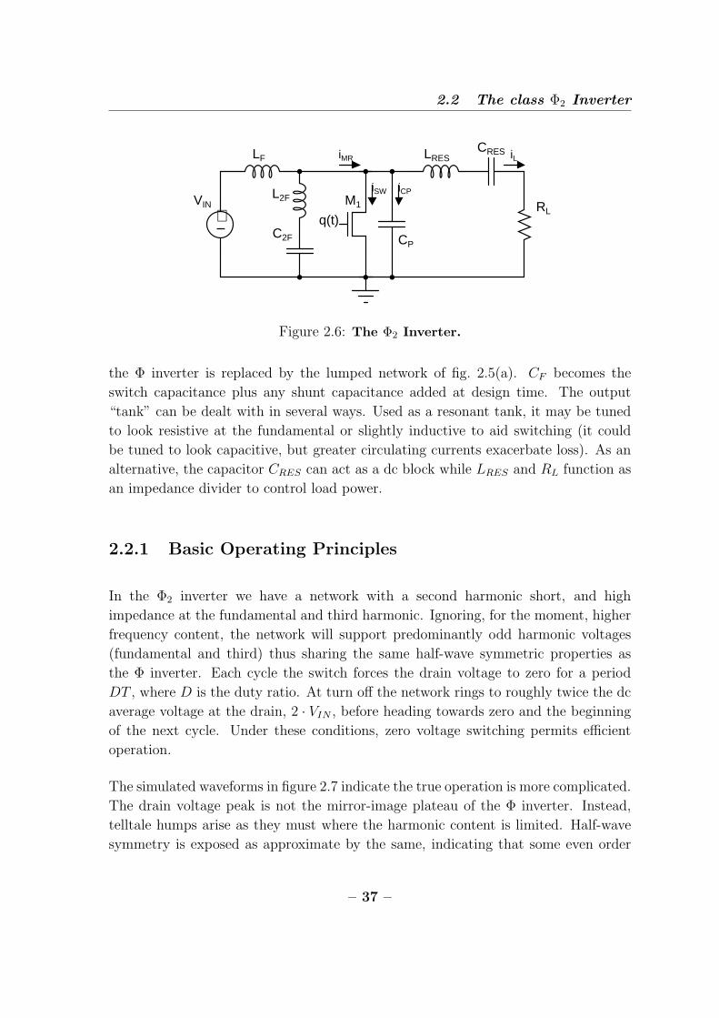
2.6 The Φ2 Inverter . . . . . . . . . . . . . . . . . . . . . . . . . . . . . . 37
2.7 Φ2 Inverter waveforms . . . . . . . . . . . . . . . . . . . . . . . . . . 38
2.8 Φ2 and transmission line responses . . . . . . . . . . . . . . . . . . . 39
2.9 Block diagram of source substitution method . . . . . . . . . . . . . . 40
2.10 Φ2 inverter split for harmonic balance analysis . . . . . . . . . . . . . 40
2.11 Φ2 network response to initial conditions . . . . . . . . . . . . . . . . 42
2.12 Duty ratio vs. harmonic composition . . . . . . . . . . . . . . . . . . 44
2.13 Φ2 drain-source impedance effects on drain voltage . . . . . . . . . . 47
2.14 Tuning sequence to increase peakiness . . . . . . . . . . . . . . . . . . 48
2.15 Tuning characteristic impedance . . . . . . . . . . . . . . . . . . . . . 49
2.16 Controlling power in Φ2 inverter . . . . . . . . . . . . . . . . . . . . . 50
2.17 Loss vs. tuning in Φ2 . . . . . . . . . . . . . . . . . . . . . . . . . . . 52
– 10 –

List of Figures
2.18 Efficiency vs. tuning in Φ2 . . . . . . . . . . . . . . . . . . . . . . . . 53
2.19 Tuning vs. transient response . . . . . . . . . . . . . . . . . . . . . . 54
2.20 Efficiency vs. characteristic impedance . . . . . . . . . . . . . . . . . 56
2.21 Φ2 inverter with nonlinear capacitance . . . . . . . . . . . . . . . . . 58
3.1 Series-loaded resonant rectifier . . . . . . . . . . . . . . . . . . . . . . 60
3.2 Φ2 boost converter . . . . . . . . . . . . . . . . . . . . . . . . . . . . 61
3.3 Series-loaded resonant rectifier in SPICE . . . . . . . . . . . . . . . . 62
3.4 Rectifier waveforms . . . . . . . . . . . . . . . . . . . . . . . . . . . . 63
3.5 AC-DC power split in rectifier . . . . . . . . . . . . . . . . . . . . . . 64
3.6 Tuning rectifier by controlling FC and ZO . . . . . . . . . . . . . . . . 66
3.7 MOSFET parasitic mechanisms . . . . . . . . . . . . . . . . . . . . . 68
3.8 Measurement Setup for RDS−ON vs. VGS and Temperature . . . . . . 70
3.9 Temperature dependence of MOSFET channel resistance . . . . . . . 71
3.10 Capacitance Measurement Setup . . . . . . . . . . . . . . . . . . . . 72
3.11 Device capacitance models compared to measurement . . . . . . . . . 73
3.12 Rectifier waveforms . . . . . . . . . . . . . . . . . . . . . . . . . . . . 74
3.13 Inverter and Converter Waveform Overlay . . . . . . . . . . . . . . . 75
3.14 Inverter and Converter Waveform Overlay . . . . . . . . . . . . . . . 77
4.1 Ranking of devices based on class-E performance . . . . . . . . . . . 80
4.2 Φ2 converter schematic . . . . . . . . . . . . . . . . . . . . . . . . . . 82
4.3 Diode current ringing around CREC-diode loop . . . . . . . . . . . . . 83
4.4 ST PD57060 Φ2 converter simulation results . . . . . . . . . . . . . . 85
4.5 Simulated and measured impedance match . . . . . . . . . . . . . . . 86
4.6 ST PD57060 Φ2 converter measurements . . . . . . . . . . . . . . . . 87
4.7 ST PD57060 Φ2 converter experimental waveforms compared to simu-lation . . . . . . . . . . . . . . . . . . . . . . . . . . . . . . . . . . . . 88
4.8 50MHz Φ2 converter simulation results . . . . . . . . . . . . . . . . . 90
– 11 –

List of Figures
4.9 Φ2 schematic with component values for BCD process . . . . . . . . . 91
4.10 Breakdown of important loss mechanisms for each prototype (simulated) 92
4.11 Experimental waveforms for the 50MHz converter . . . . . . . . . . . 94
4.12 Experimental output power and efficiency . . . . . . . . . . . . . . . 95
4.13 Converter photographs . . . . . . . . . . . . . . . . . . . . . . . . . . 96
5.1 VHF Converter Under On-Off Modulation . . . . . . . . . . . . . . . 100
5.2 Basic resonant gate drive . . . . . . . . . . . . . . . . . . . . . . . . . 102
5.3 Gate drive with shunt leg . . . . . . . . . . . . . . . . . . . . . . . . . 103
5.4 Final gate drive circuit . . . . . . . . . . . . . . . . . . . . . . . . . . 104
5.5 Converter start-up transient . . . . . . . . . . . . . . . . . . . . . . . 105
5.6 Converter shut-down transient . . . . . . . . . . . . . . . . . . . . . . 106
5.7 Converter efficiency vs. on-off modulation . . . . . . . . . . . . . . . 107
5.8 Gate drive power vs. output power . . . . . . . . . . . . . . . . . . . 108
5.9 Controller Schematic Diagram . . . . . . . . . . . . . . . . . . . . . . 109
5.10 Closed Loop Operation . . . . . . . . . . . . . . . . . . . . . . . . . . 110
5.11 Modulation frequency dependence on load and VIN . . . . . . . . . . 111
5.12 Schematic of load for load-step test . . . . . . . . . . . . . . . . . . . 111
5.13 Transient response to a load step . . . . . . . . . . . . . . . . . . . . 112
5.14 Closed-loop efficiency measurements . . . . . . . . . . . . . . . . . . . 113
B.1 Schematic of Φ2 converter with ST part . . . . . . . . . . . . . . . . . 159
B.2 Φ2 schematic with component values for BCD process . . . . . . . . . 160
B.3 Complete gate drive schematic . . . . . . . . . . . . . . . . . . . . . . 161
B.4 Complete controller schematic . . . . . . . . . . . . . . . . . . . . . . 162
B.5 ST board layout masks . . . . . . . . . . . . . . . . . . . . . . . . . . 163
B.6 ST board layout masks . . . . . . . . . . . . . . . . . . . . . . . . . . 164
B.7 BCD board layout masks . . . . . . . . . . . . . . . . . . . . . . . . . 165
B.8 BCD board layout masks . . . . . . . . . . . . . . . . . . . . . . . . . 166
– 12 –


List of Tables
3.1 Phase Shift differs for the ideal and non-ideal rectifiers when inputbias voltage and amplitude are adjusted separately. Opposingeffects of the junction capacitance cancel for the case when bothbias voltage and amplitude are adjusted simultaneously. . . . . . 67
3.2 The components of the dc-dc converter examples are listed in thistable. More detailed information including the full spice modelsand values of parasitic inductances may be found in appendix A 76
4.1 MOSFET parameters . . . . . . . . . . . . . . . . . . . . . . . . . . 81
4.2 Faichild S310, 100V, 3A Schottky diode parameters . . . . . . . . 81
5.1 Hard gating requires more than twice as much power for the cus-tom MOSFET even when the larger gate drive amplitude is ac-counted for. . . . . . . . . . . . . . . . . . . . . . . . . . . . . . . . . 102
B.1 Component values and part numbers for ST-based Φ2 boost con-verter . . . . . . . . . . . . . . . . . . . . . . . . . . . . . . . . . . . 160
B.2 Component values and part numbers for Custom-MOSFET-basedΦ2 boost converter . . . . . . . . . . . . . . . . . . . . . . . . . . . . 160
B.3 Component values and part numbers for gate drive circuit . . . . 161
B.4 Component values and part numbers for controller circuit . . . . 162
– 14 –


Chapter 1
Introduction
MINIATURIZATION has become the pursuit of modern technology. Ubiquitous
use of the term “nano-”, while often cloying, underscores the importance at-
tached to the search for the smaller. The integrated circuit stands as the benchmark
to the nano-world, a stark example of how economic power can be harnessed through
control of the tiny. While seedling ICs were analog circuits, the shrinking of digital
systems occurred much more rapidly as a relentless march on Moore’s law 1. Today,
a common theme in analog circuit design is the development of circuit topologies and
techniques that allow the realization of traditional analog building blocks—op-amps,
comparators, and the like—on the ever-shrinking CMOS processes. To the extent that
more functionality can be realized by adding analog systems to a digital substrate or
shrinking analog systems in general, there is money to be made. Take as an example
the cellular telephone. The integration of the RF power amplifier along with a host of
digital front-end signal processing has fueled the explosion of cell phone usage. While
the goal is to have everything on a single chip realizing cost, reliability, performance,
and functionality enhancements, some systems are challenging to integrate.
One particular area where integration remains largely a stymied endeavor is power
conversion. Here, the issue centers around energy storage. Most switched mode power
converters will use inductors and capacitors to fulfill the requirement. The amount of
energy storage, and therefore the numerical values of the inductors and capacitors, is a
function of the power processed, the switching frequency, and the details of the power
processing scheme [1]. Typical converters like the boost or buck converter operating
at a few tens of watts require too much energy storage to be integrated given current
process constraints. While the statement may seem cavalier, consider that typical
inductor and capacitor values for dc-dc converters on the scale of a few tens of watts
1Moore’s law is mentioned only casually here. The fact is that analog circuits require fewer devicesand benefit more from larger feature sizes and the better transistor parameters they engender. Digitalcircuits, however, rely on massive numbers of iterated structures that switch as rapidly as possible.The result has been an emphasis on shrinking the digital transistor to improve density.
– 17 –

Introduction
are measured in microhenries and microfarads, whereas integrated inductances and
capacitances are more likely to be measured in nanohenries and picofarads. Assuming
that three orders of magnitude in energy storage cannot be absorbed in an arbitrarily
small volume, and that the techniques that are the subject matter of this thesis are
not operating, the assertion is safe.
Typical inductors that might be realized on chip are in the range of a few 10s of
nanohenries and capacitors in the 10s of picofarads. The main roadblock to achieving
such small values with a conventional converter is loss. The balance of this thesis
will explore converter designs intended to circumvent typical loss mechanisms in a
manner compatible with integration and co-packaging.
1.1 Losses in hard switched converters
A switched mode power converter constructed of ideal elements has no intrinsic loss
mechanism. Rather, they arise inevitably from the use of real components. These
losses, distributed among the active and passive components constrain not only the
efficiency of the SMPS (switched mode power supply), but the size, cost, form-factor,
and even converter responsiveness. Finding ways to beat these losses is, in a sense,
tantamount to miniaturization.
On considering a typical dc-dc converter, one fact that becomes obvious is that the
bulk of the system, that is its weight and volume, comprises the passive energy storage
elements. Semiconductor devices, having benefited from tremendous improvement
since their inception, occupy only a small fraction of a typical converter footprint.
This is made clear in figure 1.1 showing a common implementation of a synchronous
buck converter where switches, gate drives, controller, startup and protection circuits,
and the housekeeping power systems are integrated onto a die and placed in a QFN
(quad flat-pack, no-lead) package. The remainder of the components are the energy
storage devices which require roughly an additional four times the board area (not
accounting for interconnect) and nearly six times the volume. It is not surprising,
then, that techniques to reduce converter footprint might be aimed at minimizing or
eliminating passive energy storage.
Where the goal is to reduce the size of the energy storage components, there are two
primary ways to proceed. Either energy density may be increased or total converter
– 18 –

1.1 Losses in hard switched converters
Figure 1.1: The synchronous buck converter components pictured will supply7.5 W into 5 V. The QFN on the left encompasses the active switches, gatedrive, control, and housekeeping functions. The remaining passive elementsrequire 4 times the board area and 6 times the volume, not accounting forboard interconnect.
energy storage reduced. Increasing the energy density implies shrinking a device for
a constant amount of storage. Even if this can be accomplished, given the physi-
cal constraints imposed by power dissipation, the increased losses that result often
cannot be reconciled with good converter performance. Considering a solenoidal in-
ductor, it is demonstrated in [2] that fundamental scaling between linear dimensions
and flux- or current-carrying area causes inductor Q to decrease as α2 where α < 1
is a constant scaling each linear dimension. Similar relationships are enumerated in
[3] for other geometries. In the case of capacitors, analogous problems arise. Where
a given dielectric material is available, a lower bound exists on the capacitor plate
separation for a set working voltage. Further, plate resistance also increases as plate
thickness is decreased or plate area is increased, both are necessary to improve en-
ergy density. These conditions imply that the capacitor Q will become unacceptably
low with continued scaling at a constant capacitance. Thus a host of factors — Q,
dielectric breakdown, and dissipation — impose a maximum energy density on pas-
sive components. Unfortunately, practical densities leave something to be desired for
converter size.
With very limited leeway to increase energy density, we turn our attention to reducing
the required energy storage. The classic solution is to raise the switching frequency
[1], thereby reducing the amount of energy processed per cycle, a condition that
leads directly to smaller numerical values of inductance and capacitance. The buck-
– 19 –

Introduction
+− LF
D1
RLVIN
COUTCINq(t)
M1
(a) Buck-boost converter
+− LF RL
VINCIN
q(t)
M1
COUT
ICH
ILD
IDCH
(b) First part of cycle
+− LF RL
VINCIN COUT
IDCH
ILD
D1
ICH
(c) Second part of cycle
Figure 1.2: In the buck-boost converter, LF acts as temporary storage. In thefirst part of the cycle LF is charged by current ICH while COUT holds up theoutput. In the second portion of the cycle LF discharges into the load whilereplenishing COUT .
boost converter in figure 1.2 is a convenient means to an explanation. The buck-
boost converter is an indirect converter. This type of converter transfers energy
from the source to intermediate storage in the first portion of a cycle and then from
intermediate storage to the load in the second portion of the cycle. The intermediate
storage in the buck-boost converter is the inductor, LF . As the switching frequency is
increased and the amount of energy processed each cycle gets smaller, the numerical
value of LF can be reduced and the inductor made physically smaller for constant
energy density. The same applies to the capacitors CIN and COUT . For instance, COUT
must hold up the output voltage during the half of the cycle when LF is charging.
The holdup time is inversely proportional to frequency as is the associated RC time
constant for a constant droop in output voltage. Another way to see that COUT can be
reduced is to consider that RL and COUT form a low-pass filter which attenuates the
switching ripple. As the switching frequency increases the low-pass corner frequency
moves up for a given attenuation, relaxing the capacitance requirement.
Though increased switching frequency attends less energy storage, it is not a tech-
– 20 –

1.1 Losses in hard switched converters
nique that may be used haphazardly: A cohort of loss mechanisms arise rapidly to
place limits on the operating frequency. While not necessarily the largest of these,
important frequency dependent losses in passive elements are limited almost exclu-
sively to inductors and their magnetic materials. Most magnetic materials, used to
increase inductance per unit volume, operate well at low frequency but have losses
that rise rapidly otherwise. The basic trend is captured by the Steinmetz equation:
Pv(t) = kfαBβ (1.1)
where Pv(t) is the time-average loss per unit volume [kW/m2], B is the peak ac flux
amplitude [Gauss], f is the frequency of sinusoidal excitation [Hz], and the constants
k, α, and β are found by curve fitting. Examining 1.1 it is clear that for α greater
than one (it’s often in the range of 1-3) that the loss will rise briskly with frequency.
Another important implication is that the core volume may be increased to reduce the
flux density, trading increased size for higher frequency—the opposite of the desired
effect2. In truth, the Steinmetz equation is only valid in a narrow range of situations,
primarily where the excitation is sinusoidal and relatively low frequency. At high
frequencies and under the non-sinusoidal excitation typical of power converters, the
losses tend to be greater than predicted in the Steinmetz model and many different
modeling approaches have been undertaken to get a more accurate prediction (for
instance, [4]). The upshot, however, is that most bulk magnetic materials are not
suitable for operation at frequencies much higher than a few megahertz.
One way of avoiding magnetic core losses is to do away with the magnetic core. The
lower energy density demands even higher operating frequencies, but to the extent
that the frequency can be increased, the magnetic loss picture looks much better. For
a simple air core inductor, the inductance and resistance are determined primarily by
geometry and the choice of conductor. Inductor quality factor Q is:
Q =ωL
R(1.2)
In this simple relationship, expressing the ratio of energy stored to energy lost per
2Often loss becomes the limiting factor at high frequency and flux derating is necessary to avoidexcessive heat build up. Thus at high frequency cored inductors can actually get larger.
– 21 –

Introduction
DBCDS
RDS
LD
LS
RG
CGD
CGS
ID
D
S
G
Figure 1.3: A MOSFET including parasitic elements usually important in hardswitched dc-dc converter design
cycle, Q increases with reactance and decreases with resistance. The frequency depen-
dence of R and L are very difficult to calculate for any geometry other than isolated
straight wires. In general, skin effect, proximity effect, and interwinding capacitance
affect both L and R [3]. If the proximity effect and the interwinding capacitance are
ignored, the skin effect results in approximately a square-root increase in resistance
with frequency. Since reactance rises linearly under these assumptions, then Q will
increase ∝ √f . Measurements of inductor Q and information available from manu-
facturers of air-core RF inductors indeed show that Q increases with frequency as a
general trend.
The seemingly synergistic effect of increasing Q with frequency for air-core inductors is
only advantageous provided that the other frequency dependent loss factors are dealt
with. These losses are associated with active semiconductor devices. Semiconductor
losses can be divided into three main mechanisms for MOSFETs: conduction loss,
switching loss, and gating loss. A MOSFET model including the parasitic elements
usually considered in dc-dc converter design is shown in fig. 1.3.
Conduction loss, due to the effective resistance of the channel, the lightly doped
drain region (LDD), and metal/bondwire resistance, is only slightly frequency de-
pendent3. Switching loss, however, depends significantly on frequency. It is helpful
3At typical operating frequencies the quasistatic assumptions for MOSFETs are valid, so the
– 22 –

1.1 Losses in hard switched converters
to further divide switching loss into overlap loss and losses resulting from discharge
of the drain-source capacitance, CDS. Overlap loss refers to the condition where
the MOSFET supports simultaneous voltage and current at its drain-source port and
thereby dissipates power. This condition arises from the need to charge or discharge
the device channel through finite source impedance (whether this impedance arises
externally or as a result of device parasitic resistance and inductance) which imposes
a minimum on switch transition times. Simplified models of overlap loss parameter-
ized in converter nominal voltage (VO) and current (IO), and MOSFET rise (τr) and
fall (τf ) times are readily available [5, 1]:
Er + Ef = kVOIO(τr + τf ) (1.3)
The constant k reflects the circuit in which the device is used and varies between
1/6 and 1/2 depending on whether the load is purely resistive or clamped inductive.
Since this result is basically fixed once the device and circuit are chosen, the energy
per transition (Er +Ef ) is also fixed. Therefore, as switching frequency rises, so does
overlap loss.
The loss due to CDS occurs at device turn on, when the energy stored on the output
capacitance is dumped into the switch yielding a loss than can be roughly approx-
imated as: 12CDSV 2
DS−PKf . This effect can be significant even at frequencies well
below a megahertz—CDS is usually fully charged just before turn-off.
Gating loss results from charging and discharging the input capacitance, CISS =
CGS + CGD. Calculating the gating loss is somewhat complicated by the presence of
CGD which is multiplied according to the Miller effect during transitions. In lateral
MOSFETs where CGD tends to be very small and its effects can be ignored, the gating
loss is approximately expressed as:
PGATE = CGSV 2GATEPK
f (1.4)
This reflects that the loss is associated with the loss of charging a capacitor from a dc
voltage through a resistor, 12CV 2, and the subsequent dumping of the stored energy
channel and LDD components of RDS−ON are constant. Bondwire resistance is usually a smallenough component that skin effect only accounts for a small change in the total RDS−ON .
– 23 –

Introduction
once per cycle. In other types of MOSFETs, such as vertical DMOS and even some
lateral devices, CGD is a significant portion of CISS and the effects can’t be ignored.
Then the gate power is usually expressed in terms of the total charge required per
cycle to enhance the device:
PGATE = QGVGATEPKf (1.5)
In both cases the frequency dependence is clearly linear. This mechanism becomes
important at switching frequencies of a few megahertz and beyond where gating loss
for typical devices can range from hundreds of milliwatts to several watts.
Diodes also account for a fraction of the converter loss budget. All diodes have an
associated forward voltage drop, VF , that combines with the forward current, IF , and
resistive losses in the bulk regions to result in diode conduction loss. This mechanism
is not explicitly frequency dependent. PN-junction diodes and PIN diodes, however,
do have a frequency dependent loss mechanism - reverse recovery. Reverse recovery
names the process in which stored minority carriers are removed during commutation.
During the reverse recovery time, τRR, the carriers are extracted across a constant
voltage. Since this time is related to the amount of stored charge and the impedance
of the external circuit, τRR is fixed for a given configuration. Therefore, the en-
ergy wasted per cycle to reverse recovery is constant implying frequency dependence.
Schottky diodes, which are formed as metal-semiconductor junctions are majority
carrier devices. They do not suffer heavily from reverse recovery losses, but are only
available with breakdown voltages below about 120 volts.
1.2 Resonant Power Conversion
Resonance, usually ascribed to systems with complex poles displaying oscillatory
behavior, is of some significance in power conversion. In filtering, for example, it
plays a role to develop large immitance in comparatively little volume4. Here we look
at resonance as a means to push back converter loss mechanisms and realize operation
4Series and parallel resonant filters can be used to shunt or block ripple in power converters. Itwas demonstrated in [6] that by using resonance, filter element volume could be reduced by betterthan a factor of three.
– 24 –

1.2 Resonant Power Conversion
+−
RL
CRESLRESLCHOKE
CPM1
q(t)
VIN
(a) Class E inverter
0 5 10 15 20 25 30 35
0
20
40
60
Time [ns]
Dra
in A
mpl
itude
[V]
Effect of Load Change on Class−E Converter Waveforms and Efficiency
2 3 4 5 6 7 8 9 1060
70
80
90
100
Load Resistance [Ω]
Effi
cien
cy [%
]
(b) 50 MHz Class E drain voltage waveforms
Figure 1.4: Resonant topologies often suffer from limited load range in powerconversion applications. Here, the Class E inverter waveforms are pictured asthe load is varied from 1
2R to 2R. The properly tuned waveform is displayed inheavy black. The loss of ZVS and negative impact on efficiency are evident.
in the very high frequency regime (VHF, 30 MHz - 300 MHz).
A number of converter topologies exist that draw from RF amplifier techniques to
achieve efficient energy conversion [7, 8, 9, 10, 11, 12, 13, 14, 15] at high frequencies.
These designs rely on reactive networks to shape the switch voltage and current and
reduce switching loss. The class E converter, fig. 1.4(a), is a widely practiced topology
whose network enforces a zero-voltage switching (ZVS) opportunity at turn-on. Its
basic operation can be classified as indirect. The inductor LCHOKE is an open at the
switching frequency, ensuring that only dc current flows from the source. With no
dc path to the load, energy from the source must first be stored on the switch shunt
– 25 –

Introduction
−
+
+−
VHFdc-dc
converter
gatedrivecomp
RH
RR
RLCBULK
VREF
Figure 1.5: Schematic depiction of VHF converter under on-off modulation.The closed-loop system keeps output voltage constant allowing the converterto deliver a constant power (effectively it sees a constant load) at it’s mostefficient point. Actual power delivered to the load depends on the duty ratio ofthe control signal.
capacitor CP . The energy stored in CP then rings towards the load in a cycle that
is determined by the switching function, q(t), and the resonant tank formed by the
load, LRES, and CRES. It functions by ringing the energy on CDS to the load once per
cycle. When these components are tuned according to [7, 8], the drain voltage will
naturally return to zero as the energy in CP rings toward the load. At this point, the
switch may be turned on with minimal loss. This mode of operation avoids the losses
usually ascribed to the switch drain-source capacitance and largely avoids overlap
loss, as well.
In practice, the drawbacks of such resonant topologies have prevented them from
seeing widespread use. To begin with, the load range is severely restricted when
compared with the 100:1 or better range achievable with conventional converters.
Resonating losses from circulating reactive currents become significant as the load
is reduced, hurting efficiency. The situation is made worse in the many cases where
the load is an integral part of the resonance. Then, any change in load disrupts
the ZVS condition and switching loss inevitably arises. This situation is depicted in
fig. 1.4(b). Further difficulty arises because duty ratio control is often not possible.
Instead, control is achieved by varying the switching frequency. The resulting poor
dynamics worsen with frequency and place an artificial upper bound on practically
achievable switching speed. Many resonant converters also suffer from high peak
switch stresses. The class E converter, in particular, has peak drain voltages rising
as high as 4.4 times the dc input voltage [16]. This is particularly troublesome where
integration is concerned because integrated devices tend to have lower breakdown
– 26 –

1.3 Contributions and Organization of the Thesis
voltages.
Several of these issues can be resolved by partitioning the energy storage and control
functions [17, 18, 19]. Instead of controlling the output by varying the switching
frequency, on-off modulation of the converter determines the fraction of output power
delivered (see fig. 1.5). When the converter is on, it delivers a fixed power maintaining
ZVS and maximum efficiency. When off, no power is delivered and there are no
associated resonating losses. Under these conditions the load range is a function of
the minimum achievable modulation index. Such operation allows the network to
be tuned to enforce ZVS at one particular operating point. The result is maximum
efficiency, better dynamics, and higher achievable operating frequency. The fact that
this mode of operation allows much higher switching frequency is self-reinforcing—
high frequency means less energy storage so the converter can be started and stopped
more rapidly and achieve a wider load range.
1.3 Contributions and Organization of the Thesis
Raising the switching frequency is a well known means of reducing required energy
storage in power converters. It is precisely this reduction that can put inductor and
capacitor values into the range that they might be considered for integration. For
inductors, in particular, VHF operation allows magnetic materials to be set aside,
avoiding the difficulty and expense of incorporating them on chip. Even so, it is not
clear that current techniques, like the planar spiral inductor, can offer high enough Q
or reasonable area. Generally, integrated inductors achieve Q’s of ten or below with
inductance in the neighborhood of 10-20 nH [20, 21]. While the techniques discussed
in this thesis result in small value inductors, the Q needs to be at least 50 or better.
Capacitors are also a challenge. Typical CMOS processes achieve about 1 fF/µm2
metal to metal capacitance. Higher density requires the use of inherently non-linear
(and potentially lossy) gate capacitance. Yet these considerations are secondary to
the question of whether or not devices available on the existing power processes are
suitable to high frequency operation. The exploration and development of techniques
that permit this answer to be “yes” is the primary contribution of this thesis.
Breakdown voltage is a key aspect in determining integrated process suitability. While
adopting resonant circuit techniques permits low loss and high frequency, it also poses
very high switch stresses. The class E converter, for instance, has an idealized peak
– 27 –

Introduction
voltage stress of 3.6 ranging up to 4.4 in practice. Since integrated processes do not
enjoy the luxury of high breakdown voltage, attempting to implement a topology like
the class E would significantly limit the input voltage range. Some RF amplifiers like
the class F are able to reduce the peak stress by waveshaping [22, 23, 24], but at the
expense of relatively high component count. In chapter 2 a new inverter we call class
Φ2 is introduced along with a tuning method that permits low peak voltage stress.
The low voltage stress achieved (2 in simulation, 2.4 in experiment) is critical to
implementing a converter with an input voltage up to 18 V on a 50 V power process,
which for instance is not possible with a class E topology. The Φ2 also has a low
component count and eliminates the need for an RF choke. With the few inductors
resonant and small, the Φ2 has excellent dynamics and makes a good candidate for
integration.
Efficient rectification compatible with integration is introduced alongside the Φ2 dc-
dc converter in chapter 3. Many resonant rectifier topologies exist for RF inverters
[13, 25, 26, 27, 28]. The particular topology set forth here offers a low component
count. When mated with the inverter the result is a resonant boost converter that
transfers power at ac and dc. The dc portion varies with the boost ratio and is advan-
tageous because it does not suffer resonating losses. Almost all the power delivered
at ac is delivered at the fundamental, where the rectifier is tuned to appear resistive.
Significantly, the rectifier tuning changes with the dc input voltage causing the output
power to vary nearly linearly with input voltage. Though this complicates design, it
offers an additional degree of freedom to tailor the desired converter behavior.
Device characterization and selection are critical. At VHF frequencies, the parasitic
components must be embraced rather than avoided. This is a key strength of the Φ2,
which can absorb the switch output capacitance as part of the wave shaping network.
Both the magnitudes and distribution of the parasitic capacitance, inductance, and
resistance are important considerations. Chapter 3 also discusses these particular
aspects, and lays out the techniques used in measuring and modeling them.
Chapter 4 presents the design and experimental results of two dc-dc converter power
stages. The first converter uses an off-the-shelf power LDMOS normally used in
RF power amplifiers. The other converter uses an LDMOS device fabricated in a
conventional silicon power process. Comparisons between the converters are drawn
that help illustrate the effects of different tuning choices at design time.
The gate drive and closed-loop performance are discussed in chapter 5. In the VHF
– 28 –

1.3 Contributions and Organization of the Thesis
regime the gate drive is not a trivial ancillary issue. Hard gating with a totem-pole
driver is out of the question. Even ignoring direct path losses in such a circuit, hard
gating loss is too high. For that reason a resonant design was employed. The two key
factors for a gate drive in this architecture are efficiency and startup time. Resonant
schemes will naturally benefit over hard gating where efficiency is considered because
some portion of the gate energy is recovered each cycle. On the other hand, direct
control of duty ratio and dynamic response are compromised. A topology and specific
tuning techniques are discussed that attempt to find the best trade offs.
Closed-loop performance is a prerequisite for having a converter, per se. In chapter 5
a voltage-mode hysteretic controller closes the loop. The hysteresis band determines
the converter peak to peak voltage ripple. A bulk capacitance in conjunction with the
load sets the modulation frequency limits. Dynamic performance is excellent as the
bandwidth is determined not by the modulation frequency, but by the delay through
the controller and the power stage dynamics, both of which are much faster.
Resonant power conversion with the Φ2 resonant boost converter can be accomplished
with transistors built from a standard power process. VHF frequencies keep energy
storage at a minimum yielding small component values and excellent dynamic per-
formance. This and a discussion of future directions for related work are presented
in chapter 6, the conclusion.
– 29 –


Chapter 2
The Φ2 Inverter
CHAPTER 1 laid out the basic considerations for conversion at VHF switch-
ing frequencies and the attendant miniaturization advantages. While resonant
conversion techniques are compelling in this regard, several key aspects make them
difficult to integrate. At the top of the list is peak switch voltage stress. In practical
implementations of the class E converter, for instance, the main switch must endure
peak voltages up to 4.4 times the input voltage. This alone is enough to break an
integrated implementation. Designs like the class F converter use wave shaping tech-
niques to reduce the switch stress, but the result is a large component count. Many
such converters also suffer from the need for a bulk inductor to function as an rf
choke at the input. This limits dynamic performance and poses yet another challenge
to integration. While variants like the second harmonic class E converter avoid this
problem, no topology yet presented offers the combination of low switch stress, low
component count, and minimal energy storage. Such a converter does exist and it is
called the Φ2 converter.
2.1 The class Φ Inverter
As an aid to our understanding of the Φ2 inverter’s operation, we briefly digress to
examine its progenitor, the class Φ inverter [2, 24]. This inverter exploits the sym-
metrizing properties of a shorted quarter-wave transmission line in order to realize
efficient high frequency conversion. The impedance characteristic of such a line is plot-
ted in fig. 2.1 where the poles appear at the odd integral multiples of the fundamental
and zeros obtain at the even integral multiples. The symmetrizing properties are ex-
posed naturally on considering the effect of driving the line with a finite-impedance
voltage source periodic in the fundamental. High impedance at the odd harmonics
blocks current, permitting the source to impress odd harmonic voltages without ef-
– 31 –

The Φ2 Inverter
50 100 150 200 250 300 350 400 450 500 550 600
−10
0
10
20
30
40
50
60
70M
agni
tude
[dB
]
Shorted Quarter−wave Transmission Line Impedance, fo=50MHz
50 100 150 200 250 300 350 400 450 500 550 600−90
−60
−30
0
30
60
90
Frequency [MHz]
Pha
se [d
eg]
Figure 2.1: Impedance characteristic of a shorted quarter-wave transmissionline.
fort. The situation is reversed for even harmonics—the line demands large currents,
nulling the source voltage. Under these conditions the periodic steady state voltage
at the driven port of the line will consist exclusively of odd harmonic components
and the current even harmonic components. The signals will then be half-wave sym-
metric and half-wave repeating respectively, a fundamental result of Fourier analysis.
By way of illustration, two signals are constructed with arbitrary combinations of
even and odd components in fig. 2.2. In each plot the sum is depicted by the heavy
line. The sum in the top plot, composed exclusively of odd components is half-wave
symmetric. In the bottom plot, the even components result in a half-wave repeating
sum.
The Φ inverter, fig. 2.3(a), consists of a shorted quarter-wave transmission line ter-
minating at the drain-source port of its switch and a resonant output tank. While
the quarter-wave line enforces drain voltage symmetry in periodic steady state, it is
the interaction of the tank with the shunt capacitance, CP (usually device parasitic
capacitance, although external shunt capacitance may be added), that ultimately
– 32 –

2.1 The class Φ Inverter
0 pi/2 pi 3pi/2 2pi
−1
−0.5
0
0.5
1
period
ampl
itude
Half−wave Symmetry
0 pi/2 pi 3pi/2 2pi
−1
−0.5
0
0.5
1
period
ampl
itude
Half−wave Repetition
Figure 2.2: Half-wave symmetric and half-wave repeating waveforms.
creates ZVS and high efficiency. Considering the waveforms in fig. 2.3(b) the drain
voltage is clearly half-wave symmetric. It has a dc average component equal to the
source voltage, a condition of achieving periodic steady state, which also serves as
the axis of symmetry. The switch holds the drain node at ground for a portion of the
cycle defined by q(t). When the switch turns off, the line current falls abruptly to
zero and the load current charges CP to the peak drain voltage, 2VIN , a value that
results from reflection about the DC average1. Once CP has charged to 2VIN , the
line current again equals the load current, and the drain voltage remains constant.
After a period equal to the switch on-time, the line current falls to zero and the load
current discharges CP , ringing the drain to zero and creating an opportunity for the
switch to turn on without loss.
It is important to note that the symmetry in drain voltage does not guarantee ZVS.
For instance the waveforms in fig. 2.4 show what would happen if the value of CP
is halved. The load network draws too much charge out of the capacitor and the
1One can also consider that the switch effectively launches a voltage wave of −VIN down theline which must return a half cycle later inverted to satisfy the boundary conditions established bythe short. With a dc average of VIN the additional VIN from the returning wave adds to the peakvoltage, 2VIN .
– 33 –

The Φ2 Inverter
+−
LRESCRES
RL
CP
quarter-wave
iLINE
iSW iCp
iL
q(t)VIN
(a) Class Φ Inverter
0 5 10 15 20 25 30 35 40 45 500
10
20
30
Time [ns]
Am
plitu
de [V
]
Φ Converter Waveforms
0 5 10 15 20 25 30 35 40 45 50
−1
0
1
Time [ns]
Am
plitu
de [A
]
0 5 10 15 20 25 30 35 40 45 50−2
−1
0
1
2
3
Time [ns]
Am
plitu
de [A
]
Vdrain
q(t)
iloadiline
iswiCp
(b) 50 MHz Class Φ Inverter Waveforms
Figure 2.3: The class Φ inverter tuned for soft switching at 50 MHz. The shortedquarter-wave line ensures the drain voltage is half-wave symmetric. The risingand falling edges of the drain voltage are due to the charging and dischargingof Cp each cycle by the difference between iline and iload. Important to note isthat the ZVS condition is not guaranteed by half-wave symmetric voltage alone.The load network and switch capacitance must interact so that the drain voltagereaches zero at the appropriate moment. See appendix A for component valuesand simulation files.
– 34 –

2.2 The class Φ2 Inverter
0 10 20 30 40 50
−10
0
10
20
30
40
50
Time [ns]
Am
plitu
de [V
]
Detuned Φ Inverter Drain Wavform for CP = C
P/2
Figure 2.4: In the Φ inverter, the transmission line enforces half-wave symmetry.When the load network and shunt capacitance CP are unmatched, loss resultsat both transitions. Component values and simulation files can be found inappendix A
drain voltage undershoots zero. The symmetry enforced by the line then causes a
corresponding overshoot one half-cycle later. This operating condition forces the
switch to dissipate energy from the capacitor each half-cycle, a lossy proposition.
Limits on power delivered to the load at a given CP , frequency, and input voltage
naturally arise where all the energy stored on CP must come from the load side. In
steady state, the load current must be exactly the right value to ring the drain to
zero. Once the duty ratio has been constrained, the tank current is fixed, and so is
the output power because the load resistance necessarily plays a role in determining
the tank current. Since CP is smallest when composed exclusively of device parasitic
capacitance, there is a minimum power delivered to the load for a given switch,
switching frequency, and input voltage. The Φ2 inverter, having the ability to absorb
device capacitance into either the load network or its source network has greater
freedom in this regard.
2.2 The class Φ2 Inverter
The class Φ2 inverter, like the Φ inverter, exploits waveshaping techniques to realize
approximate half-wave symmetry and the related benefits. It diverges on the point of
how many harmonic-coincident resonances are employed to achieve the effect. Where
the ideal Φ inverter relies on an infinite number of harmonics, the Φ2 network seeks
to control only the first three. The resulting approximate half-wave symmetry reaps
– 35 –

The Φ2 Inverter
LF
C2F
L2F
CP
ZIN
(a) Φ2 Input network
10 100 500−40
−20
0
20
40
60
80
Frequency [MHz]
Mag
nitu
de [d
B]
Input Network Impedance
(b) Bode Plot of ZIN
Figure 2.5: The impedance of the Φ2 input network can approximate a shortedquarter-wave transmission line.
the rewards of ZVS yet allows greater flexibility in establishing the details of the
waveform shape while avoiding need for many resonant elements. Key to meeting
the requirements of integration, this flexibility also comes with reduced design com-
plexity. Practical implementations of the class Φ inverter control perhaps a dozen
harmonics [2, 24]. The associated multi-resonant structures require significant design
effort, are sensitive to process variation, and difficult to change. In contrast, the
Φ2 inverter’s low-order lumped network can be readily tuned to establish a desired
impedance, reducing the design effort.
For instance, the lumped network depicted in fig. 2.5 has an impedance characteristic
that is identical to that of the shorted quarter-wave transmission line for the first
three harmonics. When the component values are selected according to eqns. 2.1 the
poles occur at the fundamental and third harmonic with a second harmonic zero.
LF =1
9π2f 2SW CF
L2F =1
15π2f 2SW CF
C2F =15
16CF (2.1)
This network can be viewed as a parallel combination of series- and parallel-resonant
tanks. The series tank, L2F and C2F , is tuned to the second harmonic, creating the
zero. The inductor LF in the parallel tank provides the low-frequency asymptote
and resonates with the other elements to create the peak at the fundamental, and
the capacitor CF provides the high-frequency asymptote resonating with the other
elements to create the peak at the third harmonic.
The addition of a parallel switch and an output tank comprised of RL, CRES, and
LRES in fig. 2.6 establishes the complete Φ2 inverter. Here the transmission line of
– 36 –
2.2 The class Φ2 Inverter
LRES
+−
M1
CRESLF
C2F
L2FVIN
CP
RLq(t)
iL
iCPiSW
iMR
Figure 2.6: The Φ2 Inverter.
the Φ inverter is replaced by the lumped network of fig. 2.5(a). CF becomes the
switch capacitance plus any shunt capacitance added at design time. The output
“tank” can be dealt with in several ways. Used as a resonant tank, it may be tuned
to look resistive at the fundamental or slightly inductive to aid switching (it could
be tuned to look capacitive, but greater circulating currents exacerbate loss). As an
alternative, the capacitor CRES can act as a dc block while LRES and RL function as
an impedance divider to control load power.
2.2.1 Basic Operating Principles
In the Φ2 inverter we have a network with a second harmonic short, and high
impedance at the fundamental and third harmonic. Ignoring, for the moment, higher
frequency content, the network will support predominantly odd harmonic voltages
(fundamental and third) thus sharing the same half-wave symmetric properties as
the Φ inverter. Each cycle the switch forces the drain voltage to zero for a period
DT , where D is the duty ratio. At turn off the network rings to roughly twice the dc
average voltage at the drain, 2 · VIN , before heading towards zero and the beginning
of the next cycle. Under these conditions, zero voltage switching permits efficient
operation.
The simulated waveforms in figure 2.7 indicate the true operation is more complicated.
The drain voltage peak is not the mirror-image plateau of the Φ inverter. Instead,
telltale humps arise as they must where the harmonic content is limited. Half-wave
symmetry is exposed as approximate by the same, indicating that some even order
– 37 –

The Φ2 Inverter
0 5 10 15 20 25 30 35 40 45 500
10
20
30
Time [ns]
Am
plitu
de [V
]
Φ2 Inverter Wavforms
0 5 10 15 20 25 30 35 40 45 50−2
0
2
4
Time [ns]
Am
plitu
de [V
]
0 5 10 15 20 25 30 35 40 45 50−2
−1
0
1
2
Time [ns]
Am
plitu
de [V
]
Vdrain
q(t)
isw
iC
p
iload
iMR
Figure 2.7: The Φ2 inverter tuned for operation at 50MHz. The drain voltagedisplays only approximate half-wave symmetry because the network only con-trols the first few harmonics. Notice that the switch current is substantiallysimilar to that of the Φ inverter (fig. 2.3(b)), but the other currents departcreating the telltale Φ2 humps. Component values and simulation files are inappendix A
– 38 –

2.2 The class Φ2 Inverter
0 10 20 30 40 50−2
−1
0
1
2
Am
plitu
de [V
]
First Three Harmonics
0 10 20 30 40 50−4
−2
0
2
4
Time [ns]
Am
plitu
de [V
]
First Six Harmonics
Vlump
Vtline
Vlump
Vtline
Figure 2.8: In the top plot both an ideal quarter-wave transmission line andthe lumped network process the first three harmonics identically. When higherfrequency content is added at equal power, the behaviors diverge. The trans-mission line still enforces half-wave symmetry, but the lumped circuit does not.
harmonics play a role in determining the drain waveform. Nevertheless, the system’s
behavior is within a stone’s throw of what might be expected: there is approximate
half-wave symmetry.
Figure 2.8 shows how the Φ2 input network and a shorted quarter-wave transmission
line compare in handling signals of differing harmonic content. When the drive current
is composed solely of the first three harmonics, all equal in amplitude, the resulting
voltage is exactly half-wave symmetric just as the shorted quarter-wave transmission
line case. When equal amplitude components of the first six harmonics are applied,
the response differs substantially from the ideal line. If the assumption of approximate
half-wave symmetry is to be valid, most of the energy in the drive signal must be in
the first few harmonics.
A useful way to define a drive signal in the Φ2 inverter is found in methods commonly
associated with the harmonic balance technique [29]. The harmonic balance tech-
nique, used as a computationally-lightweight means of solving for the steady state
response, relies on separating a circuit into a minimum set of linear and nonlinear
subcircuits. By then splitting the subcircuits at their common terminals and aug-
menting them with independent sources, each source can made to produce a drive
signal where all the terminal variables are consistent (by means of an optimization
– 39 –

The Φ2 Inverter
V(t)
+
-
I(t)
S1 S2
S2S1+−
I1(t)
V2(t)
I2(t)
V1(t)
+
-
Figure 2.9: Splitting a circuit into two subcircuits.
+−
LF
L2F
C2F
LR
CR
RL
CPVIN
q(t) V(t)
I(t)+
-
(a) Φ2 inverter
+−
LF
L2F
C2F
M1
LR
CR
RL
CPVIN +
−
V(t)
V(t)
I(t)
I(t)
+
-
SL1 SN1
A
B
A’
B’
(b) Φ2 inverter split into subcircuits
Figure 2.10: Φ2 inverter broken down into subnetworks. The network on the lefthand side of figure (b) is the complete drain-source network with drain-sourceimpedance ZAB. The MOSFET is replaced by a linear independent currentsource, I(t).
algorithm, for instance), at which point the solution is known. For example, figure
2.9 depicts a circuit consisting of two sub-circuits, S1 and S2 that share the variables
V (t) and I(t) at their terminals. The network is split as illustrated, where S1 now has
a drive current I1(t) and S2 a drive voltage V2(t). If a unique solution exists among
the branch variables of the sub-circuits, when I1(t) = I(t) and V2(t) = V (t), then
I1(t) = I2(t) = I(t) and V1(t) = V2(t) = V (t). This amounts to the substitution of
sources for subcircuits. In the case where a complete circuit is nonlinear, that portion
can be replaced with a linear source and the resulting subcircuit is linear.
When this technique is applied to the Φ2 inverter in fig. 2.10, the obvious choice
for the nonlinear sub-circuit is the only non-linear element, the MOSFET, outlined in
fig 2.10(a). The balance of the circuit forms a completely linear sub-network shown as
– 40 –

2.2 The class Φ2 Inverter
SL1 in fig. 2.10(b). With the drain voltage as the dependent variable, an independent
source I(t) is chosen to augment SL1. It is evident that this I(t) is the switch current,
what remains is to determine its harmonic content.
The harmonic balance technique does not require that the switch is substituted with
a current source. A voltage source is equally valid and a convenient means of es-
tablishing what I(t) might look like in the frequency domain. Three of the circuit
branches contain series inductors and naturally shape a current signal with tapering
high-frequency content. Even for a square-wave voltage source equal to the duty ra-
tio (the worst case physically significant source in terms of frequency content) these
branches will shape a current with diminishing signal energy above the third har-
monic. The capacitor CF has an impedance that falls with frequency and will tend to
contribute to higher order harmonic currents. However, in any real system the switch
will have a finite commutation time, limiting the frequency content. Further, while
CF may have significant current at higher frequencies, the voltage will be small due to
low impedance. The current I(t) is then the sum of the frequency components of the
four branch currents. With a network impedance as described above, having a zero
at the second harmonic and falling monotonically above the third, the drain voltage
bears out the desired characteristics—dominantly fundamental and third harmonic
content and approximate half-wave symmetry.
A time-domain view of the Φ2 inverter can also be useful. When the switch is opened,
the network is identical to SL1 (minus the current source I(t)). Upon switch closure,
CP is replaced by a short circuit. In each case, the final state of the circuit at the
switch transition is passed on as the initial conditions for the next portion of the
switching cycle. In periodic steady-state, the switch cycles on to conduct a ramping
current through LF , the returning load current through LRES, and current from the
second harmonic tank. As the switch opens, the initial conditions established by
these currents, along with energy from VIN causes the network to ring at its modal
frequencies, charging and then discharging CP . The result is the Φ2 drain voltage
waveform. In figure 2.11 the complete response of this ringing is identical to the
simulated drain voltage waveform for a period (1−D)T , at which point the switch is
cycled on to reestablish the initial conditions. The zero-state and zero-input responses
in the plot show how stored energy and energy from the source, VIN contribute to
the ringing.
At present, determining the exact component values (whether from time or frequency
domain considerations) resulting in zero-voltage, zero dv/dt switching requires nu-
– 41 –

The Φ2 Inverter
0 5 10 15 20 25 30 35 40
−10
0
10
20
30
Time [ns]
Am
plitu
de [V
]
Φ2 Drain Waveform and Response with Initial Conditions
0 5 10 15 20 25 30 35 40
−10
0
10
20
30
Time [ns]
Am
plitu
de [V
]
complete responsezero−inputzero−state
Figure 2.11: Φ2 network complete response generated by capturing the initialconditions of each state variable in the circuit of fig 2.6 just before the switchopens. The waveforms are identical over the period the switch is off. Justbefore departure, the switch closes, reestablishing the initial conditions for thenext cycle. Component values and simulation files can be found in appendix A
merical simulation. Great flexibility results from the many tuning solutions given a
desired output power, switching frequency, and duty ratio. For instance, selecting
the appropriate impedance curve and duty ratio adjusts peak voltage. Aside from
allowing the use of lower-voltage processes, the RMS values of switch conduction and
displacement currents change. Depending on the particular switch process, geometry,
and switching frequency this is a significant tradeoff. Likewise, where inductor values
are concerned, a range of characteristic impedances are achievable, and for a given
load selection of these components influences efficiency. In fact, assuming a fixed in-
ductor Q, load, and switch, an optimum characteristic impedance exists. Yet another
factor, transient performance, is related to total energy storage.
In a real inverter, the switch non-linearities complicate tuning, pushing an exact so-
lution ever further from reach. While a blind parameter sweep in SPICE will arrive
at a working design, a more informed method is desirable. The approach taken here
is to tune the inverter to a rough operating point using its impedance characteristics.
The final design, when nonlinear elements are included, is achieved by tweaking com-
ponent values based on a knowledge of the their specific impact on inverter behavior.
– 42 –

2.2 The class Φ2 Inverter
2.2.2 Tuning the Φ2 Inverter
Inverter tuning begins with the notion of approximate half-wave symmetry. While
the Φ2 input network of fig. 2.5(a) can be tuned to have peak immitances at the first
three harmonics, this does not result in zero voltage switching. The presence of higher
frequency harmonics, both even and odd, requires adjustment to the network in order
to achieve ZVS. The load also affects tuning making the total drain-source impedance,
ZAB, from fig. 2.10(b) the parameter of interest. By controlling this impedance it is
possible to tune the inverter over a wide range of operating points.
With a drain voltage signal that is necessarily periodic, the continuum of ZAB can
be largely ignored for tuning purposes. Rather, in as much as the drain voltage and
switch current can be represented as Fourier series, the discrete points at each har-
monic determine inverter operation. Thus the network need not have modal frequen-
cies at the harmonics. Instead, the magnitude and phase of the network impedance
at each harmonic, and more specifically at the fundamental and third harmonics,
determine the operational characteristics. This assumes that there is a zero at the
second harmonic. While it is possible to achieve ZVS and zero dv/dt when the zero
is only near the second harmonic, it is not necessarily desired. Over the range of
tuning points explored, pinning the second harmonic with a zero obtains the lowest
peak voltages for a given RMS conduction current proving beneficial to efficiency.
It is useful to think of the drain waveform as its Fourier series. Temporarily ignoring
higher frequencies, and remembering that the drain voltage should have no second
harmonic component, the signal is composed of a fundamental and its third harmonic
along with a dc offset equal to VIN . The shape is strictly related to the magnitudes
and phases of just these two components. In the top plot of fig. 2.12 a simulated Φ2
drain waveform is compared with the sum of its fundamental and third harmonics. It
is evident that while not exact, the approximation is reasonable. Immediately below,
a series of signals constructed with the fundamental and its third harmonic component
with zero phase offset is plotted. For each curve, the magnitude of the third harmonic
has been varied resulting in larger peaks as the ratio of the third harmonic component
increases. If these curves were to represent Φ2 drain waveforms, the switch should be
on between the close trough-pairs and off between the more distant pairs, as depicted
by the notional gate waveforms. This implies that the required duty ratio (for ZVS)
and the ratio between the fundamental and its third harmonic is related, a reasonable
result. If the drain waveform was purely fundamental the required duty ratio would
– 43 –

The Φ2 Inverter
0 5 10 15 20 25 30 35 40 45 50
0
5
10
15
20
25
Time [ns]
Am
plitu
de [V
]
Comparison of Φ2 Drain Wavform and Sum of its Fundamental and Third Harmonic Components
0 5 10 15 20 25 30 35 40 45 50
0
5
10
15
20
25
Time [ns]
Am
plitu
de [V
]
Varying Ratio of Fundamental and Third Harmonic and Required Duty Ratio for ZVS
Vdrain
V1−3
Figure 2.12: The Φ2 inverter drain waveform is primarily composed of a fun-damental and its third harmonic component as evidenced by the close matchin the top plot. The ratio of these components partially determines the dutyratio necessary to achieve ZVS; waveforms with less third harmonic require alower duty ratio. The pulse trains represent the necessary switching function,the actual value is affected by the presence of higher frequency components,but still follows the general trend.
be zero. For a drain waveform of purely third harmonic the duty ratio is close to 66%.
These extremes are not desirable. Achievable duty ratios range perhaps from 0.2 -
0.5. Within this range we find acceptable ZVS operation and gate drive requirements
that are not too severe.
The duty ratio is not solely related to the magnitudes of the harmonics, phase offset
(primarily between the fundamental and third harmonics) plays a role. Though it
adds another degree of freedom, keeping the phase offset near zero results in the
lowest peak voltage and more symmetrical waveforms. Higher frequency components
in the drain waveform also complicate matters. Clearly the construction of fig. 2.12
does not have ZVS when just the first three harmonics are considered. It is possible,
however, to achieve ZVS by an appropriate adjustment to the network impedance.
– 44 –

2.2 The class Φ2 Inverter
The resulting magnitude, phase offset, and duty ratio attain slightly different values
than otherwise predicted. These values may be divined in a numerical simulator like
SPICE and remain valid at various values of characteristic impedance2, a fact useful
when optimizing efficiency, for instance.
Tuning the Φ2 inverter brings to light an array of possible tuning points. Here we
consider two main aspects related to the shape of the drain voltage waveform and the
drain-source impedance. First, depending on the component values selected, the peak
drain voltage can range from just under 2 · VIN to greater than 4 · VIN . The “peaki-
ness” is a very important factor where device breakdown is concerned. In particular,
integrated devices tend to have lower breakdown voltages than discrete components,
and a factor of two in peak voltage can determine whether or not a design is achiev-
able in a given process. The other issue of primary importance is the characteristic
impedance of the network. This can be adjusted up or down within a range while
the peak voltage remains constant. The effect is to change the damping of the net-
work. In so doing the resonating losses change, typically reaching a minimum and
then increasing as characteristic impedance is further decreased. Component values
also change significantly, inductors shrink and capacitors get larger as impedance is
lowered. This can be exploited in co-packaging or integrated environments where
volume is at a premium. Since capacitors scale better than inductors in terms of
Q, trading higher Q capacitance for lower Q inductance is often advantageous where
very small size is desired.
Turning first to the question of peakiness highlights a useful relationship mentioned
earlier. That is, the peak drain voltage is largely determined by the ratio of the
fundamental and third harmonic magnitudes. The more third harmonic present in
the drain voltage waveform, the higher the peak voltage for a given VIN . In turn,
the voltage magnitude ratio is roughly dependent on the drain-source impedance
magnitude ratio, ZAB, at the respective harmonics. Lowering the impedance at the
third harmonic relative to the fundamental decreases the peak drain voltage because
the impedance decreases faster than the rising drive currents. Further, the impedance
relationships among the harmonics are deterministic. If the phase at the fundamental
and the magnitude ratio between the fundamental and its third harmonic are held
2The term characteristic impedance is used somewhat loosely here, being only strictly definedfor a second order system. In general, in this section it refers to shifting the impedance magnitudeup or down, usually by picking the characteristic impedance of the second harmonic leg—where itis well defined—and then reestablishing the magnitude-phase relationships at the fundamental andthird harmonics necessary for ZVS.
– 45 –

The Φ2 Inverter
constant, the converter will exhibit the same drain waveform characteristics (i.e. peak
voltage and overall shape) for a given duty ratio. It is here that a potential design
algorithm begins to emerge. If a set of magnitudes and phases are known that yield
acceptable ZVS operation, an impedance curve can be fit that produces a functional
converter. While numerical simulation is still required to derive a given set of values, it
is rather straight forward to subsequently walk along the locus of solutions and achieve
flatter and flatter waveforms. This is precisely the result presented in figure 2.13.
After a favorable tuning point is found the converter can be re-tuned by varying only
two components, LF and CF . This does not imply that the other components cannot
be varied, rather varying LF and CF is an effective means of tracing out solutions
that achieve different ratios of fundamental and third harmonic.
The procedure is demonstrated in fig. 2.14 starting with a tuned inverter at the
top left and proceeding clockwise. The waveform in the first plot exhibits ZVS and
zero dv/dt characteristics. In the second plot, the capacitor, CF has been decreased
significantly to increase the level of third harmonic. LF is then subsequently increased
until the drain waveform just reaches zero dv/dt at zero voltage. In the final plot,
the duty ratio has been adjusted (and some slight iteration performed) to get ZVS,
zero dv/dt waveforms. The component values and impedance curve that realize the
resulting drain waveform are by no means unique. However, the impedance phase at
the fundamental and magnitude ratio between the fundamental and third harmonic
along with the duty ratio constitute a set of values that when reproduced result in a
properly tuned Φ2 inverter. This remains true even as the balance of the impedance
curve varies over a wide range. As much is shown in the plots of fig. 2.15. Starting
with a tuned inverter, the characteristic impedance of the second harmonic tank is
varied. Adjusting CF and LF reestablishes the desired impedance conditions. The
result is a set of identical drain waveforms delivering constant power to the load, yet
with a circuit that has widely differing component values.
That constant load power is achieved should come as no surprise. For a given drain
voltage the current in the load leg (formed by LR, RL, and CR) is fixed. It was demon-
strated in [19] that when the drain waveform is known, the power may be estimated
by assuming most is delivered at the fundamental. Further approximating the drain
as a square wave gives a reasonable estimate of the fundamental amplitude. The
load power may then be directly calculated. Changing the load to modulate power,
however, necessarily affects ZAB, ruining ZVS. Retuning then affects the desired load
power and iteration is necessary. This dependency can be unwound by using the
impedance transfer function (eqn. 2.2) to calculate the required component changes.
– 46 –

2.2 The class Φ2 Inverter
0 5 10 15 20 25 30 35 40 45 50
0
5
10
15
20
25
30
35
Time [ns]
Am
plitu
de [V
]
Φ2 Drain Wavforms for Various Z
AB(150MEG)/Z
AB(50MEG)
(a) Φ2 drain waveforms obtained at different impedances
50 100 150 350−10
0
10
20
30
Frequency [MHz]
Mag
nitu
de [d
BV
]
Magnitude ZAB
50 100 150 350−100
−50
0
50
100
Phase ZAB
Frequency [MHz]
Pha
se [d
eg]
(b) Φ2 drain source impedance, ZAB , realizing waveforms of fig. (a)
Figure 2.13: The drain-source impedance controls the magnitude of fundamentaland third harmonic that appears in the drain voltage waveform. Lower drain-source impedance, ZAB at the third harmonic relative to the fundamental resultsin flatter waveforms. This is useful in meeting peak voltage stress requirementsand minimizing loss. Component values and simulation files may be found inappendix A – 47 –

The Φ2 Inverter
0 10 20 30 40 50
0
5
10
15
20
25
Time [ns]
Am
plitu
de [V
]
Tuned, LF = 28.8n, C
F = 354.5p
0 10 20 30 40 50
−10
0
10
20
30
40
Time [ns]
Am
plitu
de [V
]
CF reduced to 134.5p
0 10 20 30 40 50
0
5
10
15
20
25
30
Time [ns]
Am
plitu
de [V
]
Tuned, duty ratio adjusted from 0.3 to 0.38
0 10 20 30 40 50
0
5
10
15
20
25
30
Time [ns]
Am
plitu
de [V
]
LF increased to 71n
Figure 2.14: Tuning sequence to increase drain waveform third harmonic compo-nent and reduce overall circulating currents. Component values and simulationfiles may be found in appendix A
Here a brute-force MATLAB script was used to solve for new component values. By
holding the phase angle at the fundamental constant, along with the magnitude ratio
between the fundamental and third harmonic, the drain voltage does not change. This
leads to a quick method to change the output power of an existing inverter design
that avoids iteration. For example, for an existing design, the inductor LR was first
decreased from 14.1nH to 10nH to increase output power from 9.5W to 10.8W . This
change can be calculated a priori given the identical drain voltage. When the new
values for CF and LF (440pF to 497.7pF and 21.5nH to 17.343nH respectively) are
inserted in the circuit, the impedance and drain waveforms are as in fig. 2.16. In the
event that a large increase in power is required, the characteristic impedance must be
lowered. This adds an additional step to the process, but iteration can be avoided if
the load impedance is first compared to the drain-source transfer function. As long
as the impedance at the second harmonic is significantly lower than the impedance
of the load branch (at least 20dB), retuning can be accomplished as described above.
– 48 –

2.2 The class Φ2 Inverter
0 5 10 15 20 25 30 35 40 45 500
10
20
30
Time [ns]
Am
plitu
de [V
]
Φ2 Drain Waveforms as Characteristic Impedance is Changed
50 100 150 350
−20
0
20
Frequency [MHz]
Mag
nitu
de [d
BV
]
Magnitude of Drain−Source Impedance, ZAB
50 100 150 350−100
−50
0
50
100
Phase of Drain−Source Impedance, ZAB
Frequency [MHz]
Pha
se [d
eg]
Figure 2.15: Holding the constant the phase at the fundamental and the magni-tude ratio between the fundamental and its third harmonic allows characteristicimpedance to be changed without changing output power. In this case it variesfrom 5Ω to 50Ω. The component values and simulation files may be found inappendix A
ZAB =num
den(2.2)
num = LF L2F LRC2F s4 + LF L2F C2F RLs3 + LF LRs2 + LF RLs
den = LF L2F LRCF C2F s5 + LF LRCF C2F RLs4 +
(LF L2F C2F + LR(LF CF + LF C2F + L2F C2F ))s3 +
RL(LF CF + LF C2F + L2F C2F )s2 + (LF LR)s + RL
Directly calculating component values to achieve certain impedance goals extends
– 49 –

The Φ2 Inverter
0 5 10 15 20 25 30 35 40 45 500
10
20
30
Time [ns]
Am
plitu
de [V
]
Φ2 Drain Waveforms after Retune to Adjust Power
50 100 150 350−10
0
10
20
30
Frequency [MHz]
Mag
nitu
de [d
BV
]
Magnitude ZAB
50 100 150 350−100
−50
0
50
100
Phase ZAB
Frequency [MHz]
Pha
se [d
eg]
Figure 2.16: Once an operating point is established, power may be controlledby adjusting LR using the established drain voltage, Vdrain. New values of LF
and CF that are calculated using the open-switch drain source transfer function,ZAB. The calculation in this case was performed with a MATLAB script thatholds constant the phase angle at the fundamental and the magnitude ratiobetween the fundamental and third harmonics. The resulting identical drainwaveform decouples power adjustment and tuning. Here power was increasedfrom 9.5W to 10.8W . For large power increases, the characteristic impedancewill need to be lowered.
– 50 –

2.2 The class Φ2 Inverter
to other tuning aspects, as well. For instance, the characteristic impedance as was
changed in fig. 2.15 this way. First, the characteristic impedance of the second har-
monic tank, formed by L2F and C2F is raised or lowered, then values of LF and CF
are directly calculated. Since the salient impedance relationships are maintained,
the drain waveform stays constant. The utility of such a method is evident—once a
working tuning point is known an entire range may be quickly achieved. This gives
the Φ2 converter a great deal of flexibility in meeting the requirements of a particular
design.
The ability to move about the Φ2 design space with relative ease, surfaces the ques-
tion, “Where to go?” In power conversion, in general, and the co-packaged/integrated
space, in particular, there are ready compasses. As mentioned earlier, device break-
down voltage is a significant consideration with a resonant topology. Discrete transis-
tors in silicon are available with breakdown voltages of many hundreds of volts3. For
integrated power processes breakdown voltages above 100V are available, but 50V is
closer to the norm. This can be a problem with resonant converters depending on
the application. For instance, the “automotive” voltage range is generally considered
to be 8-18V . An ideal class E inverter operating over this range will have a peak
drain voltage ranging up to 65V , well beyond the typical 50V headroom in a com-
mon power process. In contrast, an ideal Φ2 inverter tuned to minimize voltage stress
has a peak voltage of roughly 2 ·VIN , in this case 36V . The practical implementations
presented in chap. 3 have realized a factor of 2.5, for a peak voltage of about 45V in
the automotive range, still comfortably within the breakdown limits.
The tradeoff associated with varying the peakiness of the drain waveform is compli-
cated by the various converter loss mechanisms. Inductor and capacitor Q determines
an effective resistance which is used to compute loss. That Q varies with frequency
is significant, but the inductors in the Φ2 inverter tend to have a dominant frequency
component. In the case of LF and LR the Q is computed at the fundamental and
L2F is evaluated at the second harmonic. Generally passive losses of significance are
constrained to inductors, capacitor Q being typically more than an order of magni-
tude better. Yet, the device capacitance, COSS, retains significance to inverter loss.
A relatively high equivalent series resistance, ROSS, confers a Q on par with the
inductors.
3Generally the device on-state resistance goes up as some power factor of the blocking voltage,so in terms of conduction loss it can be advantageous to have lower peak voltage stress
– 51 –

The Φ2 Inverter
0 100 200 300 400 5000
0.2
0.4
0.6
0.8
1
1.2
1.4
1.6
Peakiness [LF]
RMS Currents in Various Elements iSW
d
iSW
c
iL
F
iL
2F
iL
R
iC
FEX
0 100 200 300 400 5000
0.1
0.2
0.3
0.4
0.5
0.6
0.7
0.8
Peakiness [LF]
Pow
er [W
]
Power loss in various elementsp
SWD
pSW
c
pL
F
pL
2F
pL
R
pC
FEX
Figure 2.17: Sharply rising RMS currents as Zo is decreased increase overall loss.Switch displacement current, iSWd
increases for peakier waveforms, but this isoutstripped by falling conduction current loss. Component values may be foundin appendix A
Since COSS sees the drain voltage during operation, its current is therein uniquely
determined. A peakier drain voltage will have a higher RMS current both because of
its additional excursion and higher dv/dt. This becomes an important consideration in
light of ROSS. While this loss is minimized by favoring the flatter curves of fig. 2.13, it
may not be the best choice to optimize overall inverter efficiency. The plots of fig. 2.17
suggest as much. The currents and losses are plotted vs. the value of LF , of which
large values result in more peaky waveforms (for a given characteristic impedance
at the second harmonic). We see that the RMS currents in the inverter increase for
flatter drain voltage waveforms. This is not surprising when one considers how flatter
waveforms are obtained. With output power held constant, the shunt capacitance CF
must increase while LF and the duty ratio decrease to maintain ZVS. Both increasing
the capacitance and reducing the inductance lower impedance in their respective
branches and contribute to larger circulating currents. Since the load power is held
constant roughly by constraining the RMS current there, the additional circulating
currents have only two places to go: the second harmonic tank and the switch. The
increasing circulating current in the switch necessarily means that as the waveforms
are flattened, switch conduction loss increases even as displacement loss diminishes.
Though this suggests an optimum where the conduction and displacement losses cross,
it may not occur in practice. If the displacement loss is significantly smaller than the
conduction loss, often the case in practical devices when used in the Φ2 inverter, then
they may never overlap. In such a case, efficiency will continue to increase for ever
peakier waveforms (see fig. 2.18) because the drop in switch conduction and passive
– 52 –

2.2 The class Φ2 Inverter
0 100 200 300 400 50087
88
89
90
91
92
93
94Efficiency and Output Power
Peakiness [LF]
Effi
cien
cy [%
]
0 100 200 300 400 500
2
4
6
8
10
Out
put P
ower
[W]
Figure 2.18: With a fixed switch and constant output power, as the drain wave-forms get peakier, the RMS conduction current and associated losses decrease.This contributes to a rising efficiency. If a switch is used at a high enoughfrequency, or has an unusually high ROSS an optimum could occur.
component losses outweigh the increasing displacement loss.
The above discussion leaves out a number of factors that influence the optimum
tuning point. To begin with, since peakier waveforms go along with increasing LF ,
operating the inverter in that regime degrades its transient response (see fig. 2.19.
This is of particular concern in light of the intended control strategy. Modulating
the entire power stage relies on fast transient response to hold modulation losses
and bulk energy storage requirements at bay(this will be discussed in some detail in
chap. 5). Another important factor is switching frequency. As the frequency increases
a given switch will have greater displacement loss, reflecting the fact that a growing
portion of CF is being substituted with low-Q device capacitance. Under either
of these considerations, and depending on the relative magnitude of RDS−ON and
ROSS ·C2OSS, the optimum point may be different. Further, flatter waveforms require
smaller duty ratios, a concern for gate drive design (chap. 5). At VHF frequencies
resonant gate drives tend to provide the lowest loss, but most sinusoidal schemes
suffer a performance hit for non-50% duty ratios. Other schemes have limited ability
– 53 –

The Φ2 Inverter
0 50 100 150 200 250 300 350−5
0
5
10
15
20
25
30
35
Time [ns]
Am
plitu
de [V
]Effect of Tuning Point on Start−Up Transient
L
F = 41n
LF=168n
Figure 2.19: Achieving peaky drain waveforms tends to require a large inductorLF , slowing the start-up transient. Here LF is changed from 168nH to 41nH
resulting in a faster response. Component values and simulation files may befound in appendix A
to realize a wide range of duty ratios.
Monolithic devices available in an integrated implementation add another degree of
freedom. Device geometry influences the distribution of parasitic elements important
to loss, but a more direct tradeoff comes from scaling device area. As area is scaled up,
RDS−ON and ROSS decrease as COSS increases. Different than scaling frequency for a
fixed device, substituting device capacitance for CF now purchases a lower RDS−ON .
If ROSS drops linearly with area, then as area doubles displacement loss will double.
This applies so long as COSS is being substituted for discrete capacitance. Conduction
loss halves, on the other hand, and total switch loss will arrive at a minimum when
both losses are equal. The minimum device loss in this case is for a given peakiness.
The lowest total loss will still lie where the circulating currents are least, which occurs
as the drain waveform becomes more peaky.
– 54 –

2.2 The class Φ2 Inverter
In the situation where device capacitance is not replacing external shunt capacitance,
the ratio of third harmonic to fundamental will decrease (assuming, as above, that the
characteristic impedance of the second harmonic tank is held constant). Therefore
displacement loss increases even more slowly, but conduction loss may rise or fall.
This depends on whether the incremental reduction in RDS−ON outweighs the square
of the increase in conduction current that resulted from the flatter waveforms. If
conduction loss does fall, higher efficiency is obtained for less peaky waveforms (i.e.
with lower peak voltage than the device breakdown voltage, for instance). For the
very peaky tuning points, increasing the device area results in both lower peaks and
less total loss. However, the rise in RMS conduction current eventually outstrips the
increase in area, and efficiency will fall.
Characteristic impedance provides another means of optimization. For a given output
power, changing the characteristic impedance affects the stored energy. This in turn
reflects how much loss can be expected from passive components of a given Q. Using
the techniques described above on a Φ2 inverter allowed the characteristic impedance
to be adjusted from 5Ω to 50Ω. In the left-hand plot of figure 2.20 the loss breakdown
vs. characteristic impedance is presented. As characteristic impedance increases, the
loss in inductor LF falls sharply. It then settles into a gradual taper contrasting the
behavior of L2F ’s loss. This rise results as L2F increases in value and its parasitic
resistance follows suit. The increase is enough to offset the falling current and results
in an optimum efficiency (this would not necessarily be the case if an inductor of
sufficiently high Q was available, but in the VHF regime typical air-core inductor
Qs are around 100). Notice that with nearly identical drain waveforms the switch
displacement losses do not change. Similarly, the power dissipated in LR also remains
constant as its value, 16.1nH, and the load current are identical at each tuning point.
The right-hand graph in fig 2.20 offers another view of the system. The right hand
axis plots the circulating energy and the left hand axis efficiency. We see that the
efficiency peaks close to the point where the circulating energy is a minimum as a
result of falling passive losses and lower RMS conduction currents.
The flexibility of the Φ2 inverter leads to a bewildering array of design tradeoffs.
Arriving at a cut and dried procedure that always hits the best efficiency or any
other design metric is unlikely. There are, however, some basic procedures that can
help along the way, and these are enumerated below.
1. Constrain input voltage and output power
– 55 –

The Φ2 Inverter
0 50 100 1500
500
1000
1500
Characeteristic Impedance [Ω]
Pow
er lo
ss [W
]
PLF
PL2F
PLR
PSWC
PSWD
0 50 100 15072
74
76
78
80
82Efficiency and Energy Stored Per Cycle
Peakiness [LF]
Effi
cien
cy [%
]
0 50 100 15050
100
150
200
250
300
Per
Cyc
le S
tore
d E
nerg
y [n
J]
Figure 2.20: The left plot shows the most significant losses in the Φ2 inverter.Assumed inductor Q is 80, RDS−ON = 0.4, and ROSS = 0.8. Losses in L2F dom-inate for high characteristic impedance, LF losses at low Zo. The result is themaximum in efficiency shown at the right, which corresponds to the least storedenergy.
2. Assume the drain voltage may be modeled as a square wave of amplitude 4π2VIN
3. Determine the equivalent load resistance (finding an equivalent load resistance for
a resonant rectifier is discussed in chap. 3)
4. Calculate the necessary value of LR to arrive at the desired output power
5. Select a characteristic impedance of the second harmonic tank that ensures the zero
is much lower than the load impedance and the impedances at the fundamental
and third harmonic (at least 20dB)
6. Starting with the switch capacitance, tune LF to achieve a desired fundamental
and third harmonic phase and magnitude, or calculate a value with the transfer
function using predetermined phase and magnitude relationships
7. Adjust LF and CF (i.e. extra shunt capacitance) to find optimum efficiency, tran-
sient performance, or physical size. Note CF may be adjusted by increasing device
area when possible.
8. Output power may be readjusted by appropriately changing LR and calculating
new values of LF and CF using the transfer function
– 56 –

2.2 The class Φ2 Inverter
9. Adjust the characteristic impedance of the network for efficiency and component
size
10. Iterate as necessary
2.2.3 Nonlinear Capacitance Effects on the Φ2 Inverter
The device capacitance COSS is inherently nonlinear. It is primarily composed of a
reverse biased PN-junction capacitance that can be roughly modeled as eqn. 2.3
COSS(V ) =CJO
(1 + VΦbi
)M(2.3)
where CJO is the zero bias capacitance, Φbi is the built in voltage, V is the reverse bias
voltage, and M is the grading coefficient. Since COSS is a function of the reverse bias,
the behavior of the Φ2 inverter now depends on input voltage. As the input voltage
increases, the switch capacitance drops. This changes the inverter tuning. However,
the effect is not necessarily severe and COSS can be approximated for design purposes
as its value at VIN . Adjusting component values (usually just LF and CF ) is enough
to achieve ZVS. Since the inverter will only have perfect ZVS at one input voltage, the
tradeoff for maximum efficiency becomes more complicated. The specific effects of the
nonlinear capacitance in this regard are difficult to predict, and simulation is necessary
to determine the best operating point for a particular application. Figure 2.21 shows
drain waveforms for a Φ2 inverter that includes a full nonlinear capacitance model.
As the input voltage is varied, ZVS is not perfectly maintained, but the effect on
efficiency is only moderate. The effects of non-linear capacitance are dealt with more
extensively in the dc-dc converter discussions in a later chapter.
– 57 –

The Φ2 Inverter
0 5 10 15 20 25 30 35 40 45
0
5
10
15
20
25
30
35
40
Time [ns]
Am
plitu
de [V
]
Φ2 Drain Waveforms Including Non−Linear Capacitance
Figure 2.21: The Φ2 inverter waveforms shown here were generated with a modelincluding a non-linear drain capacitance. As VIN is varied, ZVS is not perfectlymaintained, but overall efficiency remains roughly constant.
– 58 –

Chapter 3
The Φ2 dc-dc Converter
WHILE there are many possible applications for the Φ2 inverter, dc-dc conver-
sion is of interest here. Such a scheme requires a suitable means of trans-
formation and rectification as well as regulation of the output. Rectification may
take a number of forms, but a practical scheme demands efficiency, low component
count, and small size, particularly where the potential for integration is desired. To
this end, a resonant rectifier is employed composed of just three components which
replace the output tank of the inverter. The resulting resonant dc-dc power stage,
under appropriate control, yields efficient operation into the VHF regime. This par-
ticular architecture of RF inverter, transformation stage, resonant rectifier was first
proposed in [11].
Appropriate control at VHF does not usually include a classic PWM scheme that
modulates the switches directly. To begin with, the operation of the Φ2 inverter
is intimately bound with the duty ratio. As discussed in chapter 2, high efficiency
operation occurs only over a very narrow range of duty ratios. Similarly, methods of
frequency control often practiced for resonant RF schemes spoil the dynamics as well
as the efficiency when control over a wide range is desired. Instead, on/off modulation
is relied upon to regulate the output [30, 18, 17]. This technique takes advantage of
the excellent transient response of the Φ2 converter, a trait gained through VHF
operation and minimalist energy storage. Not to be ignored, a classic hard-gating
scheme at VHF could be expected to dissipate energy at power levels measured in
watts. Where the desired output power is in the range of 10-20W , a more efficient
gate drive is in order. It must also include fast start-up and shut-down to fully exploit
the benefits of on/off modulation. Such a design is presented in the pages to follow
along with a host of ancillary considerations necessary to realize a Φ2 dc-dc converter.
– 59 –

The Φ2 dc-dc Converter
D1LREC
CREC COUT
VOUTVIN
+
-
+
-
Figure 3.1: The “series-loaded” resonant rectifier.
3.1 A Resonant Rectifier
Classic hard-switched (square wave) rectifiers do not scale well in frequency. Finite
commutation time and reverse recovery (when diodes are the rectifying element)
amount to untenable switching loss. In addition, resonances among parasitic junction
capacitance and package inductances are easily excited by the harmonic rich content
of a square wave rectifier voltage. Since the parasitic elements are lossy in nature,
particularly with rising frequency, the energy dumped into the oscillations counts
against rectifier efficiency [28]. Damping legs that work well at lower frequencies to
suppress these oscillations are even worse for loss as frequency increases.
A number of resonant rectification schemes have been proposed over the years [28, 11].
For instance, the class-e inverter can be used as a rectifier by replacing the switch
with a diode and interchanging the load resistance and source voltage. The result
is the time-reversed dual circuit in which power flows in the opposite direction, i.e.
from the ac-port to the dc-port, a rectifier. Many variations exist on this theme in-
cluding full-wave resonant rectifiers and dual output schemes. The particular scheme
of interest here was introduced as the “series-loaded” resonant rectifier in [28]. In
that presentation a parallel resonant tank was used across the input as a harmonic
trap. Here, the tank is dispensed with as the filtering from the combination of the
series inductor LREC and the shunt capacitance CF prove adequate. The result is the
simple rectifier appearing in figure 3.1.
In chapter 2 the point was made that in the Φ2 inverter the lion’s share of the power
delivered to the load is at the fundamental. The expected load power is then found
by approximating the drain voltage as a square wave and calculating the fundamental
amplitude. This method sized the inductor, LR, in light of the load resistance, RL.
Here, we can approximate an appropriately tuned rectifier as the load resistance RL
and use the same technique. To this end, it is useful to consider the relationship
– 60 –

3.1 A Resonant Rectifier
Lrec
Crec Cshort
D1
Cd
+−
M1Cf
Lf
C2f
L2f
Vin
Vout+
-
Ldiv
Figure 3.2: The Φ2 resonant boost converter.
between the fundamental of the drain voltage and the fundamental of the rectifier
current, as these determine the equivalent resistance in a describing function sense.
There is, however, a notable exception to this approach. Figure 3.2 shows the in-
terconnection of the Φ2 inverter and the series-loaded rectifier. The output tank of
the inverter is replaced by the rectifier which is connected across the drain-source
terminals of the switch. It should be apparent that this interconnection provides a
dc path from the source to the load in addition to carrying ac power from the in-
verter. Two important results arise from the existence of the dc path. First, the dc-dc
converter as shown is a resonant dc-dc boost converter. The output voltage cannot
drop below VIN less a diode drop. Second, the portion of the power delivered at dc
avoids the loss mechanisms associated with resonant transfer. Instead, it is subject
to parasitic dc resistance, often much lower than the ac loss mechanisms. In terms of
establishing converter output power, the dc and ac portions my be treated as roughly
orthogonal for design purposes. Equation 3.1 arises from basic conservation of energy
considerations and is useful in this regard.
PAC
PDC
=VOUT
VIN
− 1 (3.1)
It allows the determination of ac power when the total power and the conversion ratio
are known (it also shows that the fraction of ac power increases with the boost ratio,
as one would expect). Thus as a basic design procedure for the converter, one would
first determine the conversion ratio and the output power. Then having computed the
ac power from eqn. 3.1 the design proceeds by determining the equivalent resistance
of the rectifier at the fundamental. When the inverter components are sized based
on the equivalent resistance, connecting the two halves sees dc and ac power delivery
– 61 –

The Φ2 dc-dc Converter
D1LREC
CREC COUT
VOUT
VF
+−
+−
VDC
ILVREC
+
-
Figure 3.3: The SPICE scheme for tuning the resonant rectifier
roughly commensurate to the requirements of the designed total output power. Any
deviation can be easily corrected in a final design iteration.
While dc and ac power can be treated separately for purposes of designing the con-
verter as a whole, rectifier design is necessarily coupled to the dc level. The equivalent
ac resistance is a function of the dc bias (i.e VOUT −VIN) and the ac amplitude. Con-
sider the rectifier in fig. 3.3, the ac input voltage is the fundamental of the drain
voltage plus a dc bias as is produced by a Φ2 inverter. The output is tied to a fixed
voltage source of value VOUT , accurately representing the situation when the output
voltage is controlled via feedback. The time-domain results of a simulation in SPICEare presented in fig. 3.4. The top plot is the voltage at the inductor, capacitor, diode
junction under periodic steady state. When the diode is on, VREC is equal to the
output voltage, when the diode is off, CREC and LREC ring until D1 again clamps
VREC . At turn-off there are two established initial conditions, the voltage across the
capacitor equals VOUT and the current in LREC is zero (see the second plot). Thus,
after switch turn-off, iL is initially negative, reversing when the voltage on CREC has
reached its minimum. iL then increases as LREC absorbs the energy stored on the
capacitor and additional energy from the source. Once VREC rings up to VOUT the
diode again turns on and iL is shunted to the load until it reaches zero and the cycle
repeats. DC bias comes into play as it affects the magnitude of applied volt-seconds
across LREC when the diode is on. In general, when the bias is high, it will take
longer for the inductor current to reach zero. The opposite is true of a low bias. The
relationship however, is a complex one. The dc bias affects duty ratio and how much
energy is stored in the tank each cycle. In turn, the shape of the load current changes
affecting the amount of power delivered.
As it is difficult to establish a relationship among the many variables with an explicit
solution, a more pragmatic approach to tuning is favored. By comparing the voltage
and current fundamentals at the rectifier input port in SPICE, the ac power delivered
– 62 –

3.1 A Resonant Rectifier
0 5 10 15 20 25 30 35 40 45 50−40
−20
0
20
40
Time [ns]
Am
plitu
de [V
]
Rectifier Voltage and Current Waveforms
0 5 10 15 20 25 30 35 40 45 50−2
−1
0
1
2
3
Time [ns]
Am
plitu
de
iL
RECiC
REC
iLOAD
Note: iL
REC
= iC
REC
+ iLOAD
Figure 3.4: Rectifier waveforms
can be determined. The total power can be easily computed at the output port
which also gives the dc power as the difference between the two. If the fundamental
of the inverter voltage driving the rectifier can be assumed (i.e. the rectifier loads the
inverter in the same manner as the output tank), the output power is determined on
connection of the inverter and rectifier.
In order to make the assumption that the inverter voltage is a given, the rectifier
equivalent resistance needs to be determined. As mentioned above, this is readily
done by comparing the voltage and current at their fundamentals. If the rectifier in
fig. 3.3 is driven with a sinusoid of the appropriate amplitude and dc bias, the voltage
and current are in phase and the rectifier appears resistive. However, nonlinear circuit
operation means that the relationship is not true everywhere. As the dc bias or
the amplitude of the fundamental is increased the phase between the voltage and
current fundamentals, Θf , increases and the rectifier looks increasingly inductive.
When VIN = VOUT , Θf = 90 and all power is delivered at dc. This progression
is illustrated in the plots of figure 3.5. The phase can also become capacitive if
the bias or amplitude is reduced, but the voltage range over which this occurs is
narrow. Further, capacitive operation is undesirable because the circulating currents
for a given output power tend to be higher than inductive for phase, contributing to
– 63 –

The Φ2 dc-dc Converter
12 14 16 18 20 22 24 26 28 30 320
10
20
30
40
50
Input Voltage [V]
Pow
er [W
]
Power and Power Split vs. VIN
, VOUT
=33V
0 5 10 15 20 25 30 35 40 45 50
−20
0
20
40
Time [ns]
Am
plitu
de [V
]
0 5 10 15 20 25 30 35 40 45 50
−20
0
20
Time [ns]
Am
plitu
de [V
]P
TOTP
ACP
DC
VREC
Vfund
5 x Ifund
Increasing VIN
Increasing VIN
Figure 3.5: Both the total power and the split between ac and dc power deliverydepend on the dc bias and ac amplitude at the rectifier input. Componentvalues and simulation files can be found in appendix A
greater loss.
There are several important points to be made about the rectifier behavior as the dc
bias and amplitude is swept. To begin with, over a reasonable range of input voltage
bias, the output power rises sub-linearly. While the dc power is increasing, ac power
falls to zero as the duty ratio limits toward one. This can be advantageous to converter
operation because a more gradual change in power with voltage (as opposed to the
square-law resulting from a purely resistive load) relaxes the duty ratio requirements
for on/off modulation. The effect of dropping ac power delivery on rectifier efficiency
is another story. When the rectifier input appears resistive, the total power delivered
to the load for a given input voltage amplitude and bias is greatest. As the rectifier
becomes more inductive with increasing bias, circulating currents that contribute to
loss are not contributing to output power, therefore efficiency drops. One further
effect related to the changing rectifier impedance is the loss of perfect ZVS in the
dc-dc converter. While a properly tuned inverter will ordinarily maintain ZVS across
the input voltage range (assuming an ideal switch capacitance), in the dc-dc converter
the rectifier is effectively changing the output tank as dc bias and ac amplitude vary.
– 64 –

3.1 A Resonant Rectifier
Thus, an inverter coupled with a rectifier will not have ZVS over the input voltage
range. Operation without ZVS is detrimental to converter efficiency and interference
characteristics. Fortunately, proper tuning can help minimize the effect.
A useful way of tuning a rectifier for a specific resistance at a given dc bias is to choose
LREC and CREC based on their center frequency and characteristic impedance. Just
as in the case of the inverter, the characteristic impedance of the rectifier may be
varied while the overall switching behavior remains the same. The larger circulating
currents associated with lowering the characteristic impedance delivers more power
to the load for a given input voltage, changing the equivalent input resistance. On
the other hand, by changing the center frequency the rectifier input can be made to
look inductive or capacitive. Since dc bias has the same effect, this handle allows the
rectifier to look resistive at a chosen dc bias, a factor that will affect both the peak
efficiency and the efficiency vs. VIN curve of a given dc-dc converter. The plots of
fig. 3.6 bear out these dependencies. In the top plot, the center frequency is swept.
The rectifier appears resistive at the fundamental when FC is 72MHz. This value is
then used in the bottom plot where the characteristic impedance is varied from 10Ω
to 25Ω. Across the range of characteristic impedance, the result is identical switching
behavior, but higher circulating currents and therefore lower equivalent resistance.
As another consideration for tuning, the aforementioned variation of rectifier impedance
with input voltage is reduced as the rectifier is tuned to look more inductive. Since
tuning the rectifier further away from resistive operation decreases efficiency there is
potentially a tradeoff between maintaining good ZVS and high efficiency. However, in
practical designs high efficiency has tended to outweigh ZVS. Nonlinear device capac-
itance also has a role to play. One might expect that as VIN increases, the effective
junction capacitance will increase, driving down the resonant frequency of the LREC-
CREC tank. The result should be an even greater shift in the waveforms with bias.
This does happen under some circumstances, but the effect may not be pronounced
depending on the particular device and voltage range. Comparing a rectifier with an
ideal diode and one that uses a diode with a nonlinear junction capacitance (in this
case an S310) is illustrative. First, the non-ideal rectifier was tuned to look resistive
at VIN = VF = 12V . Holding LREC constant, the ideal rectifier was then tuned to
the same conditions (resistive at 12V ) by adjusting CREC . As the bias is swept from
12V to 18V the resulting phase shift between the two rectifiers differs slightly. In the
ideal case, the phase shift is 25.4 whereas the non-ideal rectifier displays a slightly
larger shift of 28.2. The small change in effective capacitance of the diode junction
over this voltage range accounts for this small difference. This could be larger for a
– 65 –

The Φ2 dc-dc Converter
0 5 10 15 20 25 30 35 40 45 50−15
−10
−5
0
5
10
15
Rectifier Waveforms as FC
is swept from 65MHz to 75MHz
Time [ns]
Am
plitu
de [V
]
0 5 10 15 20 25 30 35 40 45 50
−30
−20
−10
0
10
20
30
40
Time [ns]
Am
plitu
de [V
]
VFrec
iFrec
increasing Fc
Vrec
iload
(a) Rectifier waveforms as FC is swept
0 5 10 15 20 25 30 35 40 45 50−15
−10
−5
0
5
10
15
Rectifier Waveforms as ZO
is swept from 10Ω to 25Ω
Time [ns]
Am
plitu
de [V
]
0 5 10 15 20 25 30 35 40 45 50
−30
−20
−10
0
10
20
30
40
Time [ns]
Am
plitu
de [V
]
iload
Vrec
VFrec
iFrec
(b) Rectifier waveforms for ZO sweep
Figure 3.6: The rectifier may be tuned by adjusting FC and ZO. In fig. (a), therectifier becomes progressively more inductive for higher FC . The bold tracesare in phase at FC = 72MHz. Fig. (b) shows that changing ZO only affects thecurrent (and hence equivalent resistance). VREC remains unchanged. Tuningthe rectifier is easily accomplished by selecting FC so the input is resistive atthe fundamental and then tuning ZO to realize the desired resistance value.Component values and simulation files may be found in appendix A
– 66 –

3.2 The Power Stage
Case Ideal Rectifier Rectifier w/ Junction CapacitanceΘf , Bias Only 25.4 28.2
Θf , Amplitude Only 28.2 25.3
Θf , Amp. and Bias 43 43
LREC 59.717nH 59.717nHCREC 98.51pF 50.11pF
Table 3.1: Phase Shift differs for the ideal and non-ideal rectifiers when inputbias voltage and amplitude are adjusted separately. Opposing effects of thejunction capacitance cancel for the case when both bias voltage and amplitudeare adjusted simultaneously.
different junction capacitance or over a different voltage range. Interestingly, if the
dc bias is held fixed and the amplitude of the fundamental is varied, the behavior is
the opposite. The diode effective capacitance decreases with amplitude and this time
the nonlinear diode circuit has less phase shift, 25.3 vs. 28.2 than the linear circuit.
This is important when both the amplitude and dc bias are changed to mimic the
case of an actual inverter as the source. Under these conditions, both rectifiers have
an identical phase shift of 43. The opposing behaviors of the junction capacitance
with dc bias and ac amplitude seem to largely cancel over the test range. The results
are summarized in table 3.1.
3.2 The Power Stage
Having enumerated the salient characteristics of both a Φ2 inverter and a candidate
rectifier, it remains to connect the two together and arrive at a dc-dc converter.
In this case, as discussed in the previous section, when the Φ2 inverter is mated
with the series-loaded rectifier, the result is a Φ2 resonant dc-dc boost converter.
The details of interconnection are no more complicated than the substitution of the
output tank for the rectifier. Important considerations, however, lie in choosing the
appropriate equivalent resistance for the rectifier and at what input voltage it appears
resistive. The characteristic impedance of the network also deserves examination,
though driven by device selection and operating frequency. Device selection is critical,
in the medium power range of 10-20W where prototype converters were constructed,
devices dominate the loss budget. Therefore, before proceeding device characteristics
of particular importance to the Φ2 converter will be examined.
– 67 –

The Φ2 dc-dc Converter
DBCDS
RDS
LD
LS
RG
CGD
CGS
ID
D
S
GROSSLG
Figure 3.7: The MOSFET parasitic elements important to Φ2 converter opera-tion must be accounted for at design time.
3.2.1 Important Device Characteristics
Real semiconductor devices include parasitic elements important to the operation of
the Φ2 converter. Both MOSFETs and diodes used respectively as the active devices
in the inverter and rectifier are important in this regard. Figure 3.7 shows a model of
a MOSFET. The channel resistance RDS−ON is of primary importance, and in most
suitable devices represents the dominant loss mechanism. ROSS and COSS take a close
second. The displacement currents flowing through COSS during the drain excursion
each cycle amount to significant loss in ROSS. The value of COSS sets this current
along with the drain voltage and switching frequency (iCOSS= Cdv/dt). It also
influences the range of characteristic impedance that can be achieved. When COSS
comprises the entirety of CF , the minimum achievable characteristic impedance at
a given frequency is reached. This influences both the conduction and displacement
currents and the corresponding loss from RDS−ON and ROSS. Thus as a figure of merit
(ignoring gate drive concerns and assuming dominantly conduction loss) the product
RDS−ONC2OSS offers a rough indication of device performance in the Φ2 converter. The
gate resistance RG and input capacitance CISS are also important. Under sinusoidal
resonant drive the gating loss is described by eqn. 3.2,
Pgate = (πCISSVacfSW )2RG (3.2)
where Vac is the amplitude of the sinewave and fSW is the fundamental frequency.
– 68 –

3.2 The Power Stage
Other drive methods exist such as resonant trapezoidal gating which offers lower
loss [30], but sinusoidal gating is preferred here for simplicity. From the equation it
is evident that the gate loss rises linearly with RG and as the square of CISS. In the
10-20W power range with typical devices, the gate loss can be several percent of the
total power processed, and care must be taken to minimize this loss.
The gate to drain capacitance CRSS has a significance all its own. Whatever the gate
drive scheme selected, the current conducted through CRSS as the drain transitions
must not unduly influence the gate voltage. In terms of device selection this poten-
tially excludes many vertical devices which have much larger CRSS than the LDMOSdevices used for prototyping. It also implies that the impedance looking back from
the gate (into the gate drive circuit) must be small enough that the voltage is con-
trolled by the gate drive. In the case of the sinusoidal drive, the resulting drain-gate
transfer function was critical in achieving the appropriate operating frequency. This
will be discussed in more detail in the chap. 5
The parasitic inductances arising primarily from packaging constraints can be sig-
nificant to Φ2 converter operation. In many cases it is desirable to augment COSS
with external shunt capacitance (usually to control the peak voltage as discussed in
chap. 2). In this case, the loop inductance resulting primarily from LS and LD can
result in ringing that may affect converter behavior, and ultimately increase loss. In
addition, LG and LS can make gating difficult as ringing at the gate may cause the
switch to commutate several times per cycle and render a converter design infeasible.
Ringing at the gate as well as across the drain source terminals is reduced to an
extent by the smooth transitions characteristic of resonant operation. However, the
non-linear parasitic capacitances and behavior of the rectifier act to upset ZVS intro-
ducing high frequency components that may excite the resonances. As a result the
package inductance is best minimized and packaging is sought that achieves this goal.
In many cases, devices used in RF applications have special packaging that specifically
addresses parasitic inductance and works well in Φ2 converter applications. In this
work the first converter was constructed with such a device (an STMicroelectronics
PD57060 in a POWERSO-10RF package) and follow-on prototypes were built with
a custom die in a 20-pin TSSOP package where all 20-pins were used for the three
device terminals to minimize inductance. In both cases, loop inductance was held to
less than 1nH which was sufficient to prevent interference with converter operation.
Diode parasitics are similarly important. Junction capacitance influences both achiev-
able Zo and the circulating currents in the rectifier. The effective resistance of the
– 69 –

The Φ2 dc-dc Converter
+−
+−
DMM
DMM AGILENT
HOT
VGSDR
AIN
34410A
BIAS
34410AAGILENT
PLATE
Figure 3.8: The MOSFET was biased to ID = 1A and VDS measured to determinechannel resistance. Temperature is controlled by a hot plate.
drift region is significant to loss, as is the forward voltage drop. Reverse recovery
losses characteristic of minority carrier devices like the conventional P-N junction
diode, are largely avoided with Schottky diodes, favoring their use at VHF frequen-
cies. In the prototypes constructed, diode loss was the second biggest loss mechanism
underscoring the importance of finding an appropriate device.
The values of the many parasitic elements were extracted by a variety of measurement
techniques. In the case of the MOSFET, RDS−ON was measured versus VGS by biasing
Id to one amp and measuring VDS. A schematic of the test setup can be found in
fig. 3.8. The further dependence of on-resistance with temperature was measured by
affixing the devices to a hotplate to get VDS vs. junction temperature. A similar
technique to extract forward drop vs temperature was used on the diodes. The
MOSFET data is plotted in fig. 3.9.
Device capacitances were measured using an Agilent 4195A in impedance analyzer
mode. CDS, CGS and, CGD were extracted vs. voltage by taking three sets of two-
terminal measurements under bias. The various measurement setups are shown in
fig. 3.10. The same measurements were used to obtain ROSS by taking the impedance
at the self-resonant frequency (where COSS and the parasitic inductance of the mea-
surement loop are resonant) during measurement A (in fig. 3.10). ROSS was also
measured vs. temperature on a hot plate and it was found to have roughly the same
temperature coefficient as RDS−ON .
The resulting set of small-signal capacitances was used to reconstruct the large signal
capacitance behavior by curve-fitting the measurements to the depletion capacitance
model mentioned in chap. 2. This approach should remain valid for very high frequen-
– 70 –

3.2 The Power Stage
2 4 6 8 10 12 14 16 18 20100
200
300
400
500
600
700
800
VGS
[V]
RD
S−
ON
[mΩ
]
RDS−ON
vs. VGS
, parameterized in temperature for custom MOSFET
T=25.6°T=49.5°T=76°T=98.5°T=117.8°T=135.3°
(a) RDS−ON vs. VGS
20 40 60 80 100 120 140150
200
250
300
350
400
Temperature [° C]
RD
S−
ON
[mΩ
]
RDS−ON
vs. Temperature for Custom MOSFET
VGS
=7.5V
GS=10
VGS
=12.5V
GS=20
(b) RDS−ON vs. Temperature
Figure 3.9: Temperature dependence of the channel resistance of the customMOSFET used in this thesis
– 71 –

The Φ2 dc-dc Converter
+−
+−
+−
ac s
hort
measurementportVbias
Rbi
g
Rbi
g
Rbi
g
Vbias Vbias
measurement
measurement
port
port
COSS=CDS+CGD CISS=CGS+CGD CA=CDS+CGSC)B)A)
Figure 3.10: Since the MOSFET capacitances cannot be measured directly,three measurements are required to extract the values. An Agilent 4195Ain impedance analyzer mode was used to measure the capacitance at 1MHz.
cies as the quasi-static assumption does not break down unless changes take place
on the order of the dielectric relaxation time, which is typically much shorter than
the switching periods of interest. This is supported by the experimental results of
chapter 4. In SPICE both CGS and CGD were modeled as linear capacitors. COSS,
on the other hand, was modeled using a behavioral current source to simulate the
nonlinearity. The plots in fig. 3.11 show the match between the spice model and
measured results for both diode and MOSFET capacitance.
3.2.2 Linking the Inverter and Rectifier
Armed with device models that include parasitic elements, we are now in a position
to assemble a dc-dc converter from a rectifier and inverter. The design begins with a
rectifier. The desired output power is 17.3W . The rectifier will be tuned to appear
resistive at the fundamental when the input voltage is 14V and the output voltage
is 33V . To start the design an ideal diode is used with a capacitance equivalent to
the diode capacitance at the dc bias, 19V . For this diode with CJO = 267.77pF ,
M = 0.42, and VJ = 0.365, the equivalent capacitance is 50.43pF . With the 50MHz
sinusoidal input set to a 14V bias and the fundamental amplitude of 16V 1 the center
frequency FC of the LREC-CREC tank is swept until the fundamental voltage and
current are in phase, which occurs at FC = 68MHz. At this point, the characteristic
impedance can be adjusted until the desired output power is met, this occurs at
ZO = 24Ω. The final values for LREC and CREC are 56nH and 47pF respectively, after
1In this case, the amplitude of the fundamental was determined based on a previous inverterdesign. Since the aim is to reproduce the impedance characteristics of that inverter to get the samedrain voltage waveform, extracting the fundamental beforehand is fine.
– 72 –

3.2 The Power Stage
0 5 10 15 20 25 30 35 400
50
100
150
200
250
300S310 Schottky Diode Measured Capacitance vs. Spice Model
Reverse Bias [V]
Cap
acita
nce
[pF
]
MeasurementModel
(a) Diode Junction Capacitance
0 5 10 15 20 25 30 35100
150
200
250
300
350
400
450Drain−Source Capacitance vs. Bias Voltage, Custom Die
VDS
[V]
Cap
acita
nce
[pF
]
Modeled COSS
Measured COSS
(b) MOSFET COSS
Figure 3.11: Nonlinear device capacitance plots showing measured values vs.the model. The spice model parameters for the diode are as follows: CJO =267.8p, M = 0.420, VJ = .365. The spice model parameters for the MOSFET are:CJO = 425.2p, M = 0.253, VJ = 0.177. Detailed device models can be found inappendix A
– 73 –

The Φ2 dc-dc Converter
0 5 10 15 20 25 30 35 40 45
−10
0
10
Time [ns]
Am
plitu
de [V
]
In−Phase Fundamental Rectifier Voltage and Current
0 5 10 15 20 25 30 35 40 45−40
−20
0
20
Time [ns]
Am
plitu
de
Voltage at Anode of D1
0 5 10 15 20 25 30 35 40 45
0
10
20
30
Time [ns]
Am
plitu
de [V
]
Input Voltage and Current
VF(REC)
5 x IF(REC)
VIN
IIN
Figure 3.12: The nominal waveforms of a tuned rectifier. Note that the funda-mental voltage and current are in phase allowing the rectifier to be representedas a resistor in a describing function sense.
the 50pF equivalent switch capacitance is extracted. When these values are included
in a simulation of the rectifier with the full diode model and all parasitic elements
(inductor Q = 80 and capacitor Q = 5000) the result is an output power quite close
to 17.3W . Figure 3.12 shows the rectifier waveforms and the in-phase fundamental
voltage and current (rectifier input current is multiplied by 5 for visibility). The next
step is to extract the rectifier equivalent resistance, in this case VFREC/IFREC
which
gives Req = 7.63Ω.
Under the assumption that the ac and dc power delivered to the load can be treated
separately, the ac power that the inverter should deliver can be calculated from
eqn. 3.1 as 10W . Using the fundamental of the inverter drain voltage and the equiv-
alent resistance of the rectifier, 7.63Ω, the value for the divider inductor LDIV is
computed as 20nH. The inverter is then tuned to achieve the desired impedance
characteristic. In this case, it is known that ZVS will be achieved for a fundamen-
tal phase, Θf = 35.818 and a drain voltage magnitude ratio fundamental:third
– 74 –

3.2 The Power Stage
0 5 10 15 20 25 30 35 40 45
0
5
10
15
20
25
30
Time [ns]
Am
plitu
de [V
]
Minimal Effect on Inverter Waveforms on Rectifier Connection
0 5 10 15 20 25 30 35 40 45−15
−10
−5
0
5
10
15
Time [ns]
Am
plitu
de
Fundamental of Rectifier Voltage and Current, Nearly in Phase
InverterConverter
VoltageCurrent
Figure 3.13: Nearly identical drain waveforms between the inverter and con-verter show the minimal effect connecting the rectifier has on inverter opera-tion. Similarly, the fundamental voltage and current are nearly in phase as isthe case when the rectifier is driven solely with a fundamental voltage.
harmonic, ∆1−3 = −2.01dB. The dc-dc converter components that realize this
impedance relationship are listed in table 3.2.2. The output power is 10W as de-
sired.
When the inverter and rectifier are connected, the result should be identical drain
waveforms and an output power of 17.3W . While the drain waveforms are almost
identical (see fig. 3.13, the output power is only 15.3W , about 11% low. This arises
because the rectifier equivalent resistance is a function of both the dc bias and the ac
amplitude of its drive voltage. However, correcting the power is relatively straightfor-
ward. The inductor LDIV is adjusted in the dc-dc converter until the desired output
power is achieved. The new value is LDIV = 13nH. ZVS can then be reestablished
by again tuning the inverter to meet the same impedance characteristic. The result is
a higher inverter output power of 12.5W . When the original rectifier and readjusted
inverter are mated, the drain voltage waveforms are almost identical and the output
– 75 –

The Φ2 dc-dc Converter
Component Initial dc-dc Converter Final dc-dc Converter (17.3W )LF 24.23nH 39.06nHCF 54.4pF 121pFL2F 78.32nH 78.32nHC2F 32.34p 32.34pFLDIV 20nH 13nHLREC 56nH 56nHCREC 47pF 47pF
Duty Ratio 0.3 0.3fSW 50MHz 50MHzVIN 14V 14VVOUT 33V 33VPOUT 15.3W 17.3W
Table 3.2: The components of the dc-dc converter examples are listed in thistable. More detailed information including the full spice models and values ofparasitic inductances may be found in appendix A
power is 17.3W as intended. While the procedure requires some iteration, it can be
accomplished quickly. The final components values are listed in the second column
of table 3.2.2. The final dc-dc converter waveforms are presented in fig. 3.14.
– 76 –

3.2 The Power Stage
0 5 10 15 20 25 30 35 40 45
0
5
10
15
20
25
30
Time [ns]
Am
plitu
de [V
]
Minimal Effect on Inverter Waveforms on Rectifier Connection
0 5 10 15 20 25 30 35 40 45−15
−10
−5
0
5
10
15
Time [ns]
Am
plitu
de
Fundamental of Rectifier Voltage and Current, Nearly in Phase
InverterConverter
VoltageCurrent
Figure 3.14: After the output power is corrected, the dc-dc converter behavesjust as in the initial example. Nearly identical drain waveforms between theinverter and converter and in-phase rectifier voltage and current show the min-imal effect connecting the rectifier has on inverter operation.
– 77 –


Chapter 4
Converter Prototypes
THE following pages present a few prototype converters supporting the augury
of the preceding chapters as having some basis in fact. Two designs represent
an initial implementation using an off-the-shelf RF power MOSFET and a follow-on
built with a custom device. The off-the-shelf component served as the main switch
in the first Φ2 converter, a proof of concept. The custom device was made in a
standard BCD power process and mounted in a 20-pin TSSOP package. Converters
constructed with this device are intended to demonstrate the feasibility of using an
standard power process to realize a VHF converter in the Φ2 topology.
4.1 The First Prototype
As a prelude to constructing a prototype, a target application in the automotive
operating range was selected. This includes an input voltage range from 8V -18V with
normal operation in the range of 11V -16V . The output voltage dictated by the specific
application, in this case LED headlamp drivers, is selectable over a range of 22V -
33V . Nominal output power is about 20W . While this application doesn’t require
the fast transient response of the Φ2 converter, it does require a boost converter. It
also makes a good starting point because the input voltage and output power are
well matched to the capabilities of a Φ2 converter based on the available 50V process
device. For instance, a lower input voltage range for the same output power demands
higher circulating currents. Since resonating losses rise as the square of the circulating
current, an application with a lower input voltage or much higher output power would
be an unreasonable target for a first attempt at building the Φ2 converter topology.
Choice of operating frequency is subject to the dual constraints of the semiconduc-
tor parameters and the existing frequency allocations provided by the FCC. Taking
– 79 –
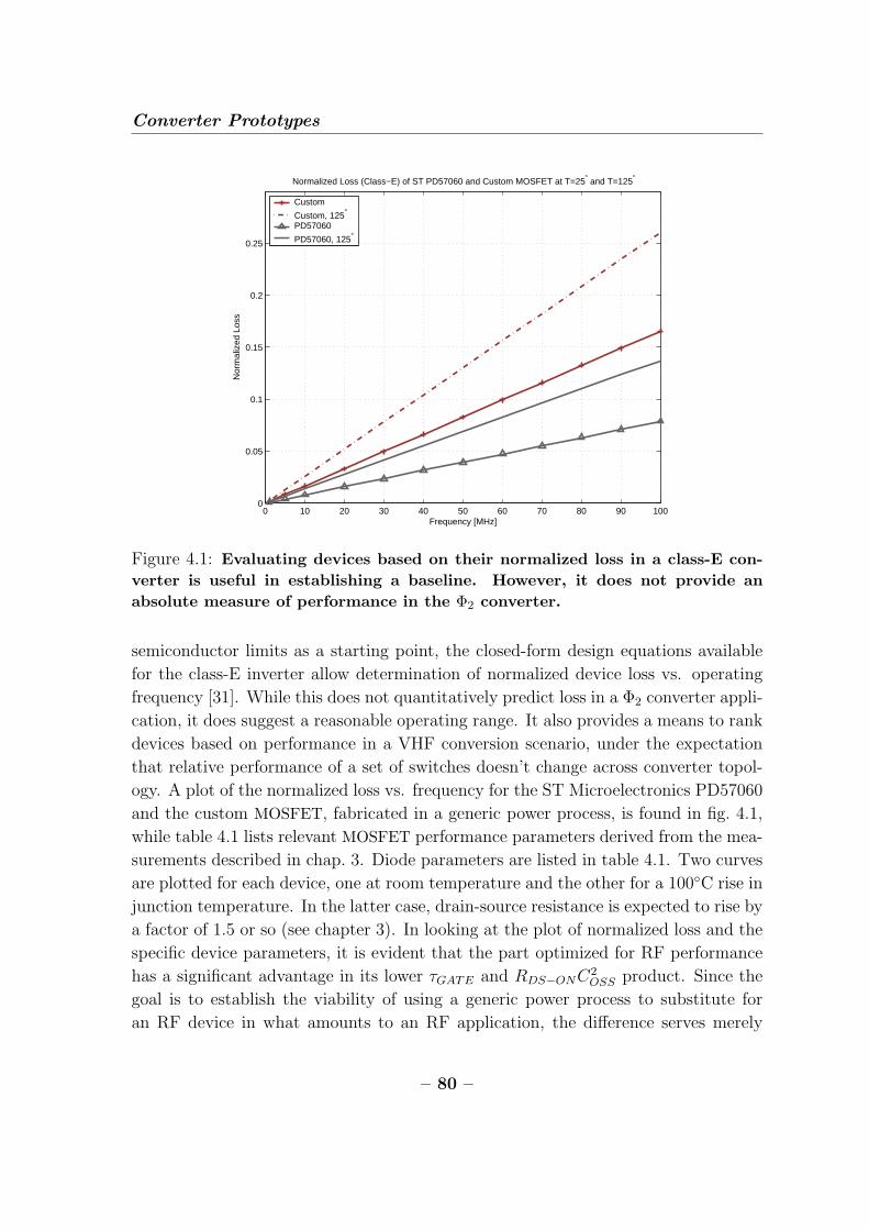
Converter Prototypes
0 10 20 30 40 50 60 70 80 90 1000
0.05
0.1
0.15
0.2
0.25
Frequency [MHz]
Nor
mal
ized
Los
s
Normalized Loss (Class−E) of ST PD57060 and Custom MOSFET at T=25° and T=125°
Custom
Custom, 125°
PD57060
PD57060, 125°
Figure 4.1: Evaluating devices based on their normalized loss in a class-E con-verter is useful in establishing a baseline. However, it does not provide anabsolute measure of performance in the Φ2 converter.
semiconductor limits as a starting point, the closed-form design equations available
for the class-E inverter allow determination of normalized device loss vs. operating
frequency [31]. While this does not quantitatively predict loss in a Φ2 converter appli-
cation, it does suggest a reasonable operating range. It also provides a means to rank
devices based on performance in a VHF conversion scenario, under the expectation
that relative performance of a set of switches doesn’t change across converter topol-
ogy. A plot of the normalized loss vs. frequency for the ST Microelectronics PD57060
and the custom MOSFET, fabricated in a generic power process, is found in fig. 4.1,
while table 4.1 lists relevant MOSFET performance parameters derived from the mea-
surements described in chap. 3. Diode parameters are listed in table 4.1. Two curves
are plotted for each device, one at room temperature and the other for a 100C rise in
junction temperature. In the latter case, drain-source resistance is expected to rise by
a factor of 1.5 or so (see chapter 3). In looking at the plot of normalized loss and the
specific device parameters, it is evident that the part optimized for RF performance
has a significant advantage in its lower τGATE and RDS−ONC2OSS product. Since the
goal is to establish the viability of using a generic power process to substitute for
an RF device in what amounts to an RF application, the difference serves merely
– 80 –

4.1 The First Prototype
Parameter PD57060 Custom MOSFETRDS−ON , TNOM , VGS = 8V 211mΩ 200mΩ
RDS−ON , T + 100C 350mΩ 350mΩCOSS,VDC = 16V 68pF 132pF
RDS−ONC2OSS 924ΩpF 2 3480ΩpF 2
CISS 100pF 276pFRGATE 195mΩ 1.7ΩτGATE 47ps 469.2psROSS 655mΩ 600mΩCJO 185.2pF 416.3pFM 0.221 0.233VJ 0.168 0.117
Ldrain 400pH 400pHLsource 200pH 100pHLgate 400pH 600pH
Table 4.1: MOSFET parameters
VFWD RSER RCJCJO VJ M CJNOM
ESL0.55V 300mΩ 300mΩ 267.8pF 0.365 0.420 50.4pF 1nH
Table 4.2: Faichild S310, 100V, 3A Schottky diode parameters
to illustrate the point. It ultimately manifests as a set of design tradeoffs made to
exploit the different devices.
For the PD57060, assuming a 100C temperature rise, the normalized loss tips over
10% right around 75MHz. This makes a convenient design frequency because it falls
just below the FM band (88MHz - 108MHz) while still high enough to ensure small
passive components. The choice represents a certain amount of judgement as the
device loss in the Φ2 converter will be different than in a class-E converter.
An initial design was simulated in spice based on a 75MHz switching frequency and
the target voltages and power. The resulting component values are indicated on the
schematic in fig. 4.2. Several practical issues were exposed during the course of the
design. First, additional shunt capacitance intended to reduce the peak drain voltage
caused excessive ringing with the package inductance. The 100pF originally added
across the switch and the approximately 1nH loop inductance associated with the
packages and routing form a resonance with a relatively low characteristic impedance
(about 2.5Ω). In this range, damping is out of the question as it would incur too
– 81 –

Converter Prototypes
Lrec
Crec Cshort
D1
Cd
+−
M1Cf
Lf
C2f
L2fVin
Vout
+
-
Cshort
81p 14x100n
35.5n130n
22n
51p
12x100n
S310
PD57060
Figure 4.2: Final component values of Φ2 converter implemented with STPD57060.
much loss. The alternative, removing additional capacitance, had to be compensated
in the design by increasing the value of LF from 28nH to 130nH. This became the
largest inductor in the design, whose volume increases the difficulty of realizing either
a co-packaged or integrated implementation. It also affects the transient response of
the converter as in chapter 3, though this is less of a concern because the resulting
transient response is still quite good. While not a factor here, another issue that
could arise, particularly in an integrated design, is the resulting higher peak voltage
stress. This points to the need to either reduce package parasitic inductance to the
point where it is no longer a concern, or have continuous control over the device area
to control impedance without additional capacitance.
Another design-time choice included tuning the rectifier to look relatively inductive.
In this regime, the change between the voltage and current fundamental components
as the input voltage changes is reduced. This minimizes the effect of rectifier non-
linearity on the ZVS characteristics of the inverter. If this was a critical component
of the design, perhaps for minimizing converter emissions, it may be well justified.
However, it corresponds to a reduction in efficiency because the ac component of
power delivery accompanies larger circulating losses than in the resistive case. Where
efficiency is paramount, tuning the rectifier to appear resistive within the operating
range is a better option. This was the case in the second prototype, as will be
discussed shortly.
Ringing in the loop around the main switch was not the last word in that regard.
The series combination of CREC and the diode junction capacitance also resonate
with the parasitic inductance around the CREC-diode loop. The loop is highlighted
in figure 4.3, along with a simulation of the diode current. In simulation, the ringing
– 82 –

4.1 The First Prototype
Lrec
Crec Cshort
D1
Cd
Vout
+
-81p 14x100n
35.5n S310
Ringing
Lpar
~3n
50.4p (nom)
~520MHz
(a) Diode-CREC loop
0 5 10 15 20 25 30 35−3
−2
−1
0
1
2
3
4
5
Am
plitu
de [A
]
Time [ns]
Simulated Diode Current in ST Converter
(b) Diode current due to ringing
Figure 4.3: Ringing among the diode capacitance, CREC , and the parasitic in-ductance results in increased diode loss due to larger circulating currents.
results near 530MHz, consistent with the 31pF equivalent capacitance in series with
the 3nH loop inductance. The relatively large excursions increase the circulating
currents in the diode to the point that its power dissipation limits would be exceeded
if left unchecked. To circumvent this problem, converter output power was lowered
at the expense of an overall reduction in efficiency.
Similarly to the main switch case, the necessity of an external capacitor CREC is at the
root of the problem. It is essentially in parallel with the diode junction capacitance,
and added to achieve the desired characteristic impedance. Since the impedance
is dictated by the choice of converter operating point, it is a difficult tradeoff to
avoid. Discrete diodes do not offer a continuous range of junction capacitance, and
compensating by changing LREC may not be feasible. On the other hand, when
the diode area can be scaled, as in an integrated process, no external capacitance is
necessary. This eliminates the loop and ringing. The parasitic inductance around the
loop in question as part of LREC , and scarcely noticed except for an offset in output
power provided reasonable care is taken to minimize loop area.
The simulated output power and efficiency vs. input voltage from the resulting de-
sign are presented in fig. 4.4(a) where the output voltage was held constant. The
same variables are plotted vs. VOUT in fig. 4.4(b) while VIN is held at 14V , auto-
motive nominal. In both plots the efficiency rises monotonically as the amount of
dc power delivery increases (dc power delivery increases with decreasing conversion
ratio, therefore it is higher for larger VIN in the first plot and smaller VOUT in the
second). This is an artifact of a rectifier that looks inductive at the fundamental over
– 83 –

Converter Prototypes
the voltage sweep range. Since ac power delivery will be relatively inefficient in this
case, increasing the proportion of dc power improves total efficiency. This has the
overall effect of reducing the peak efficiency because there is never a situation where
ac power delivery is particularly efficient. The situation is different when the rectifier
is tuned resistive within the input voltage range, as in the second prototype.
The converter was constructed on a 4-layer PCB. A photograph of the board is shown
in fig. 4.13(a) and schematics and PCB artwork are provided in appendix B. The
choice of four layers was not due to routing concerns. Rather, the prepreg material
that separates the top and bottom copper from the inner layers is very thin, on the
order of 10 mils in this case. When the inner layers are used as a ground plane (in
fact, three of the four layers were ground in this design), the parasitic inductance is
much reduced over what could be expected with a normal 2-layer FR4 board. This
makes building the converter easier as fewer board parasitics mean fewer component
changes in compensation. It also helps efficiency as trace parasitic inductance tends
to be low Q. In general, parasitic inductance and capacitance must be considered
when laying out the board and during construction. Thus, extensive inter-layer vias
to ground were used where possible to ensure good ground connections and reduce
inductance. Where low inductance was required between components, traces were
kept wide and short. At nodes sensitive to capacitance, narrow traces were placed
above ground plane notches.
As was established in chapters 2 and 3 converter dynamic performance can be pre-
dicted if the desired impedance across the drain-source port of the switch is attained.
Thus, the overarching procedure to realize a working converter involves developing a
time-domain simulation in SPICE with the desired characteristics and then trying to
match its drain-source impedance when building the prototype. Since parasitic com-
ponents can affect this impedance significantly, they must be accounted for. Rather
than explicitly computing board parasitics with a simulator, the design approach in-
volved minimizing the parasitics using the rules of thumb described above, followed by
careful measurement during the construction phase. Measurement was accomplished
with an Agilent 4195A in impedance analyzer mode. A jig was fabricated to connect
the PCB to the analyzer. Besides providing a low-inductance electrical connection,
the jig is a mechanically stable platform so measurement to measurement parasitics
are consistent.
Construction begins by shorting the drain-source node of the circuit board, then
measuring the loop inductance of the jig. The jig is constructed to keep parasitic
– 84 –

4.1 The First Prototype
8 9 10 11 12 13 14 15 16 17 1870
75
80
85
90
Simulated Efficiency and Output Power in ST Converter, LREC
= 35.5n
VIN
[V]
Effi
cien
cy [%
]
8 9 10 11 12 13 14 15 16 17 18
10
15
20
Out
put P
ower
[W]
(a) Efficiency and power vs. VIN at VOUT =32V
22 23 24 25 26 27 28 29 30 31 32 33
80
81
82
83
84
85
86
87
Simulated Efficiency and Output Power in ST Converter
VOUT
[V]
Effi
cien
cy [%
]
22 23 24 25 26 27 28 29 30 31 32 33
10
11
12
13
14
15O
utpu
t Pow
er [W
]
(b) Efficiency and power vs. VOUT at VOUT =32V
Figure 4.4: Simulated Φ2 converter power and efficiency. Note the monotonicbehavior of power with voltage that results from the inductively tuned rectifier.
– 85 –

Converter Prototypes
0 50 100 150 200 250 300
−10
0
10
20
30
40
50
Frequency [MHz]
Mag
nitu
de Im
peda
nce
(dB
Ω)
Magnitude Impedance vs. Frequency
Spice SimulationCompensated
Figure 4.5: The compensated measurement compares well with the simulateddrain-source impedance.
capacitance (and hopefully inductance) to a minimum, but it must be calibrated out.
After mounting a board with shorted drain and source nodes, the loop inductance of
the jig assembly can be measured. Thus, any remaining parasitic inductance can be
subtracted point-by-point from further measurements. The converter is then built up
one branch at a time, starting with the second harmonic short. Parasitic elements are
either compensated with component changes or accounted for in a SPICE simulation
to ensure the effects are minimal. A more detailed discussion of this method can
be found in [19]. The final result is a good match between measured and simulated
drain-source impedance as displayed in fig 4.5.
Fig. 4.6 plots the measured converter output power and efficiency. The general trends
from the simulation of fig. 4.4 are well represented. Specific differences are not easily
accounted for, but probably involve thermal effects, among others. There is a signifi-
cant difference between output power at the upper range of VIN . This may be partly
due to inadequate measurement of parasitic elements, as output power is particularly
sensitive to the value of LREC . On the other hand, the experimental waveforms of
fig. 4.7 match simulation rather well.
This converter did not include a gate drive. Instead, the gate of the PD57060 was
driven directly from an RF power amplifier (an AR-150A100B) with a 50Ω output
impedance. This worked well for the purposes of verifying the viability of the Φ2
– 86 –

4.1 The First Prototype
8 9 10 11 12 13 14 15 16 17 1870
75
80
85
Measured Efficiency and Output Power in ST Converter, LREC
= 35.5n
VIN
[V]
Effi
cien
cy [%
]
8 9 10 11 12 13 14 15 16 17 18
5
10
15
20
Out
put P
ower
[W]
(a) Efficiency and power vs. VIN , VOUT =32V
22 23 24 25 26 27 28 29 30 31 3281
82
83
84
85
86
87
Measured Efficiency and Output Power in ST Converter, LREC
= 35.5n
VOUT
[V]
Effi
cien
cy [%
]
22 23 24 25 26 27 28 29 30 31 32
10
10.5
11
11.5
12
12.5O
utpu
t Pow
er [W
]
(b) Efficiency and power vs. VOUT , VIN=14V
Figure 4.6: The measured output power and efficiency
– 87 –

Converter Prototypes
0 5 10 15 20 25 300
5
10
15
20
25
30
35
40
45
Time (ns)
Am
plitu
de (
V)
Drain Source Voltage for Vin
=8V to Vin
=18V, 2V steps
(a) Drain waveforms plotted over VIN
0 5 10 15 20 25 30 35
−20
0
20
40
Time [ns]
Dra
in a
nd G
ate
Am
plitu
de [V
]
Comparison of Simulated and Measured Waveforms, VIN
=14V
MeasuredSpice
0 5 10 15 20 25 30 35
−20
0
20
40
Time [ns]
Rec
tifer
Vol
tage
[V]
MeasuredSpice
(b) Comparison between measured and simulated converter waveforms
Figure 4.7: The measured and simulated converter waveforms agree closely as aresult of the good impedance match.
– 88 –

4.2 A Second Prototype
converter as a power stage in this operating regime. However, it also obscured gate
losses. These were calculated based on the assumption of sinusoidal resonant gating
and accounted for in the experimental efficiency data, a relatively minor effect for the
PD57060.
Gating loss is not so easily dismissed in the case of the custom MOSFET. That
device has a significantly larger gate time constant (table 4.1). Thus, a converter
constructed at 75MHz is not viable with this device. While the power stage works
well, the gating loss is two orders of magnitude larger than the PD57060 at the same
frequency, about 460mW . Coupled with a practical gate drive, this could easily
amount to a 5% reduction in efficiency. A significant improvement may be had by
scaling the switching frequency to 50MHz. Then the ideal sinusoidal gating loss is
204mW and can be expected to cost only 1-2% in efficiency.
4.2 A Second Prototype
The purpose of this prototype is to demonstrate the feasibility of using a conventional
power process at VHF frequencies as opposed to a discrete device optimized for RF.
Using such a device opens the possibility of a future, completely integrated converter.
Besides offering the benefits of low cost and small size, integration can also allow
the optimization of a device to a particular converter. Unfortunately, there was no
opportunity to optimize or even design the device in question for this implementation.
It was a sample provided for the purpose of evaluating the feasibility of using the
process. Thus the converter had to be designed around the switch taking into account
its various strengths and shortcomings, a process which provides useful contrast with
the first prototype. It also establishes the viability of using a power-process device in
a VHF converter.
A larger gate time constant is not the only efficiency related consideration for the
custom MOSFET. The RDS−ONC2OSS product is 3.8 times larger than that of the
PD57060. This implies larger device loss for a given output power. Fortunately, in
the Φ2 converter, the loss and output power is not fixed directly. Rather, a change
in tuning point can alter the loss picture. In the first prototype, maintaining ZVS
was favored over ultimate efficiency. Here, by tuning the rectifier to be resistive over
some portion of the input voltage range, device shortcomings can be overcome to a
degree.
– 89 –

Converter Prototypes
10 11 12 13 14 15 16 17 1870
71
72
73
74
75
76
77
78
79
80Simulated Efficiency and Output Power in 50MHz Converter
VIN
[V]
Effi
cien
cy [%
]
10 11 12 13 14 15 16 17 18
8
10
12
14
16
18
20
22
24
26
Out
put P
ower
[W]
(a) Efficiency and power vs. VIN , VOUT =32V
22 23 24 25 26 27 28 29 30 31 32 3371
72
73
74
75
76
77
78Simulated Efficiency and Output Power in 50MHz Converter
VOUT
[V]
Effi
cien
cy [%
]
22 23 24 25 26 27 28 29 30 31 32 3312
13
14
15
16
17
18
19
Out
put P
ower
[W]
(b) Efficiency and power vs. VOUT , VIN=14V
Figure 4.8: Simulated power and efficiency.
– 90 –

4.2 A Second Prototype
Lrec
Crec Cshort
D1
Cd
+−
M1Cf
Lf
C2f
L2fVin
Vout
+
-
Cshort
47p 8x100n
56n22n
22n
115p
8x100n
S310
BCD PROC.
Cextra
56p
Figure 4.9: Final component values of Φ2 inverter implemented with the inte-grated power process device.
Rather than pursue a different operating point altogether, the converter was designed
for the same application, an automotive LED headlamp driver. The input and output
voltage ranges are the same, 8V -18V and 22V -33V , respectively and the output power
remains in the 20W range. In this particular converter, achieving reasonable efficiency
in light of the poorer switch parameters demanded that the rectifier be tuned to look
resistive. In this scenario the phase between the voltage and current fundamentals
changes rapidly as the input voltage moves around the center voltage1. For instance,
decreasing the voltage causes rectifier current to lead voltage (at the fundamental) and
the rectifier to appear capacitive. This has two important effects. First, as mentioned
in chapter 3, operating a rectifier with capacitive phase increases circulating current
for a given output power, thus hurting efficiency. Secondly, the rectifier begins to
look capacitive because the drive voltage falls off, but only over a narrow range, less
than two volts in this case. Dropping the input voltage further actually causes the
rectifier to stop functioning. The diode never turns on and converter output power
and efficiency collapse.
While it is desirable to pick the nominal input voltage as the center voltage to max-
imize efficiency there, this will limit the low end of the input range. On the other
hand, moving the center voltage too low means that efficiency at the nominal op-
erating point will suffer. Here, with difficult switch parameters, the center voltage
was chosen as 12V . This causes a steep drop-off in efficiency at low input voltage
and trims one volt off the usable operating range (i.e., input voltage must be greater
than 9V ). However, efficiency at the nominal operating point is 2% greater than if
1For the purposes of this discussion the term, “center voltage,” refers to the input voltage atwhich the rectifier fundamental voltage and current are in phase, assuming the nominal outputvoltage of 32V .
– 91 –

Converter Prototypes
8 9 10 11 12 13 14 15 16 17 180
200
400
600
800
1000
1200
1400
Pow
er [m
W]
VIN
[V]
Simulated Loss Breakdown in ST Converter, LREC
= 35.5n
PSW
PDIODE
PL
RECP
LF
PL
2F
(a) Loss breakdown with PD57060
10 11 12 13 14 15 16 17 180
500
1000
1500
2000
2500
3000
3500
Pow
er [m
W]
VIN
[V]
Simulated Loss Breakdown in 50MHz Converter
PSW
PDIODE
PL
RECP
LF
PL
2F
(b) Loss breakdown with custom MOSFET
Figure 4.10: Breakdown of important loss mechanisms for each prototype (sim-ulated)
– 92 –

4.2 A Second Prototype
the full input voltage range was maintained. Since 8V is an unusually low bus in an
automobile, such a scenario could be dealt with in a contingency fashion.
A design undertaken with the above considerations in mind produced the simulated
power and efficiency results in fig 4.8. The plot in fig. 4.8(a) is interesting. The
efficiency peaks around VIN = 12V as intended, the point where the rectifier appears
resistive. Higher voltage sees a drop in efficiency as the rectifier starts to look inductive
and lower voltage sees a steeper drop while the rectifier heads to the capacitive regime.
The final design component values are listed on the schematic in figure 4.9. In this
design, the largest inductor is 56nH, a significant reduction over the 130nH inductor
of the previous design. Also notable, is the much smaller LF = 22nH, which is
beneficial to transient performance.
A comparison between the loss breakdown of each prototype helps to clarify why the
tradeoff between input voltage range and efficiency was necessary in this prototype
as compared to the first design. In figure 4.10 one can see just how different the
switches are. In the case of the custom small MOSFET, its losses greatly outstrip
the others, even at the lower frequency where switch displacement losses should fall
and inductor Qs are relatively poorer. This is in contrast to the converter that uses
the PD57060, where the diode loss exceeds the switch loss at high input voltage. The
latter is partially due to the larger ringing in the 75MHz converter. In the second
prototype, the diode losses are roughly 20% lower despite higher output power. It
should be noted that since COSS and circulating currents are proportional, the device
output capacitance figures into device loss as a square term. The ability to control
the device area, which is ordinarily available to an integrated process could improve
the picture significantly if the converter operating point is assumed fixed.
The construction technique was the same as the first prototype, a 4-layer board min-
imizes parasitic inductance. A photograph of this prototype is shown in fig. 4.13(b)
and a detailed schematic and PCB artwork are shown in appendix B In this case,
the gate drive and control circuits are located on the board. Their presence does
not affect the power stage operation because of extensive use of the ground planes.
Detailed information on the gate drive and control circuits is covered in chapter 5.
Tuning is performed in identical fashion, with an impedance analyzer to verify the
drain-source port impedance match to simulation. The result, when the converter
waveforms are plotted next to their SPICE compatriots, is consistent with the good
match observed with the previous prototype (see fig. 4.11(a)).
– 93 –

Converter Prototypes
0 5 10 15 20 25 30 35 40 45 50−10
−5
0
5
10
15
20
25
30
35
Time [ns]
Am
plitu
de [V
]
Comparison of Measured and Simulated Converter Waveforms, VIN
=14V
MeasuredSpice
(a) Comparison of measured and simulated waveforms
0 5 10 15 20 25 30 35 40 45 50
0
5
10
15
20
25
30
35
40
45
Time (ns)
Am
plitu
de (
V)
Drain Source Voltage for VIN
=10V to VIN
=18V, 2V steps
(b) Drain waveform progression with input voltage
Figure 4.11: Experimental waveforms in the 50MHz converter
– 94 –

4.2 A Second Prototype
8 9 10 11 12 13 14 15 16 17 18
68
69
70
71
72
73
74
75
76
77
78
Measured Efficiency and Output Power in 50MHz Converter
VIN
[V]
Effi
cien
cy [%
]
8 9 10 11 12 13 14 15 16 17 18
8
10
12
14
16
18
20
22
Out
put P
ower
[W]
(a) Measured power and efficiency vs. VIN
22 23 24 25 26 27 28 29 30 31 3272
72.5
73
73.5
74
74.5
75
75.5
76Measured Efficiency and Output Power in 50MHz Converter
VOUT
[V]
Effi
cien
cy [%
]
22 23 24 25 26 27 28 29 30 31 3210
11
12
13
14
15
16
17
18
19
20
Out
put P
ower
[W]
(b) Measured power and efficiency vs. VOUT
Figure 4.12: Experimental output power and efficiency
– 95 –

Converter Prototypes
(a) 75MHz converter with ST PD57060 switch
(b) 50MHz converter with custom MOSFET
Figure 4.13: Converter pictures. Note the calibration marks indicating a dimen-sion of 1”. While the images remain rectified, they are scaled relative to oneanother. The top converter is actually larger, each side corresponding roughlyto the long dimension of the converter in fig(b).
– 96 –

4.2 A Second Prototype
The experimental drain waveforms for various input voltages are plotted in fig 4.11(b)
followed by the measured output power and efficiency in fig. 4.12. The same charac-
teristic peak in efficiency vs. input voltage is observed. The efficiency at the peak
is within 1% of the simulated value, but it occurs at a slightly lower voltage. This
means that the actual converter can be operated down to 8V , but the efficiency leaves
something to be desired. It also contributes to a 3% lower efficiency at 18V , rather
than the 1% observed at the peak. Finally, pictures of both converters are included
for requisite ogling.
It’s worth noting that both converters using the Φ2 topology have peak voltage stresses
significantly less than an equivalent class-e design. Stresses below 45V , rather than
the 65V + expected in a class-e, are advantageous where the use of integrated devices
is desired. This matches well with the elimination of bulk inductance characteristic
of other resonant designs. This again makes the case for realizing an integrated
implementation, particularly in light of the reasonable efficiency obtained with an
un-optimized power process device.
– 97 –


Chapter 5
Closed-Loop Operation
POWER conversion, in the dc-dc arena at least, almost exclusively demands some
form of closed-loop control. The need to impose an output voltage or current
under changing load and input conditions assures it. In RF converter topologies
including the Φ2 converter, this can be a somewhat thorny issue. The requirements
for fixed duty ratio and load run counter to the notion of regulation, often a change
there is tantamount to poor efficiency. As outlined in chap. 1, separation of the
energy storage and regulation functions by choice of control strategy is VHF converter
catharsis. In much the same way that soft-switching utilizes parasitics rather than
fighting them, control using a “bang-bang” scheme takes advantage of the one thing
that a VHF converter with minimal energy storage has in spades; transient response.
5.1 Control Scheme
The rough-out of the control scheme introduced in the first chapter is redrawn in
fig. 5.1. A Φ2 dc-dc converter supplies the load which is shunted with bulk capacitance.
The output voltage has a sawtooth ripple characteristic, rising while the power stage
is energized and falling otherwise. This, in turn, is subject to the presence of the
sinusoidal waveform produced by the gate drive, itself controlled by a logic signal. The
logic signal originates at the output of a comparator with hysteresis that determines
the output voltage and its excursion (i.e. the ripple).
Under the assumption of small ripple, the converter runs at nearly the same operating
point over a modulation cycle, delivering constant power at its output. Thus, bang-
bang control modulates power delivered to the load via the fraction of the time that
the converter is on, rather than the switch (as in a conventional boost). Further, by
also avoiding frequency control methods, the energy storage elements can be tuned
– 99 –
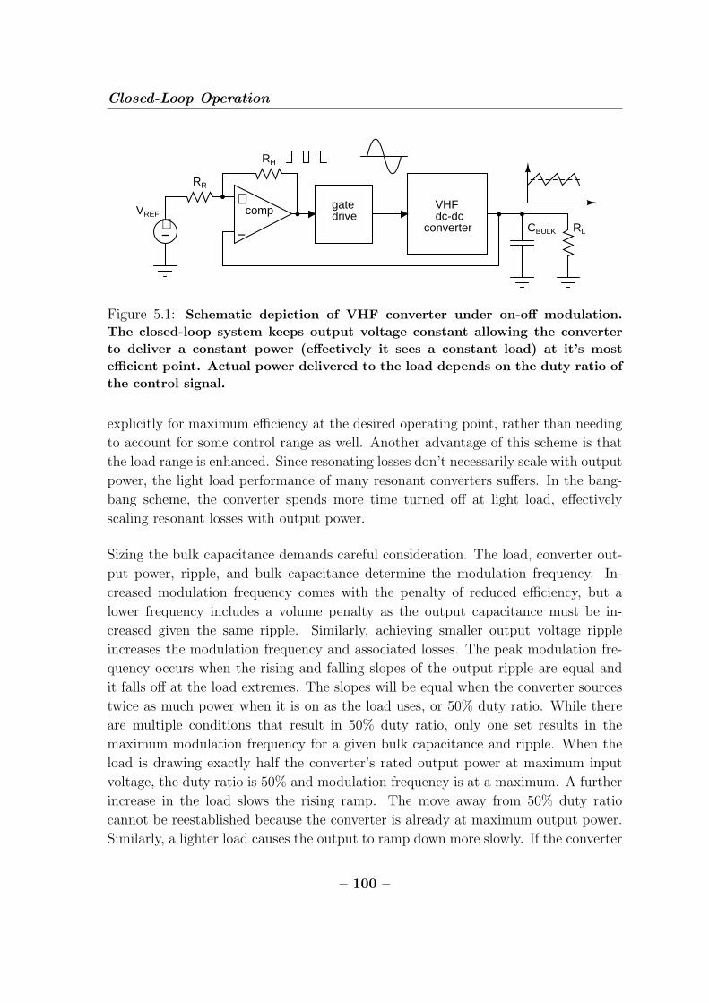
Closed-Loop Operation
−
+
+−
VHFdc-dc
converter
gatedrivecomp
RH
RR
RLCBULK
VREF
Figure 5.1: Schematic depiction of VHF converter under on-off modulation.The closed-loop system keeps output voltage constant allowing the converterto deliver a constant power (effectively it sees a constant load) at it’s mostefficient point. Actual power delivered to the load depends on the duty ratio ofthe control signal.
explicitly for maximum efficiency at the desired operating point, rather than needing
to account for some control range as well. Another advantage of this scheme is that
the load range is enhanced. Since resonating losses don’t necessarily scale with output
power, the light load performance of many resonant converters suffers. In the bang-
bang scheme, the converter spends more time turned off at light load, effectively
scaling resonant losses with output power.
Sizing the bulk capacitance demands careful consideration. The load, converter out-
put power, ripple, and bulk capacitance determine the modulation frequency. In-
creased modulation frequency comes with the penalty of reduced efficiency, but a
lower frequency includes a volume penalty as the output capacitance must be in-
creased given the same ripple. Similarly, achieving smaller output voltage ripple
increases the modulation frequency and associated losses. The peak modulation fre-
quency occurs when the rising and falling slopes of the output ripple are equal and
it falls off at the load extremes. The slopes will be equal when the converter sources
twice as much power when it is on as the load uses, or 50% duty ratio. While there
are multiple conditions that result in 50% duty ratio, only one set results in the
maximum modulation frequency for a given bulk capacitance and ripple. When the
load is drawing exactly half the converter’s rated output power at maximum input
voltage, the duty ratio is 50% and modulation frequency is at a maximum. A further
increase in the load slows the rising ramp. The move away from 50% duty ratio
cannot be reestablished because the converter is already at maximum output power.
Similarly, a lighter load causes the output to ramp down more slowly. If the converter
– 100 –

5.2 A Resonant Gate Drive
input voltage is reduced until the duty ratio is 50% once more, then both the rising
and falling ramps are slower than the half-load case. Thus once the ripple and load
range are known, the maximum modulation frequency can be set by selecting the
bulk capacitance at half-load.
The maximum modulation frequency does not necessarily correspond to the greatest
loss due to modulation. Instead, conditions where the duty ratio is very small or
very large can have higher loss at a given frequency. This arises because over very
short periods the converter is spending less time in steady-state operation where its
efficiency is greatest. Light-load efficiency may suffer in this regime, for instance. The
load range may be extended by ensuring that both the gate driver and the converter
have fast transient response so that steady-state operation is reached as quickly as
possible.
5.2 A Resonant Gate Drive
The constant duty ratio and fixed operating point of the Φ2 converter are a good
match with a resonant gate drive. At VHF, the latter offers much higher efficiency
than the totem pole drivers common at lower frequency. While the power lost to
simple hard gating can be estimated as Pgate = CISSV 2Gf , as in chap. 2, this does
not include losses in the driver itself, such as direct path loss caused by overlap at
device turn-on, which becomes important at VHF. Even so, under sinusoidal resonant
gating, the loss is closer to Pgate = (πCISSVacfSW )2RG as in chap. 3 which can be
much lower than the hard gating case.
CISS vs. bias voltage for the custom MOSFET is plotted in fig. 5.2. Since the gate
needs to swing to at least 6V to ensure the MOSFET is fully enhanced, the effective
CISS is 276pF . The equivalent gate resistance is 1.7Ω for an approximate gate time
constant of 469ps. These values are used in computing the loss for both hard gating
and sinusoidal resonant gating in table 5.2. In evaluating the sinusoidal gating loss,
a higher voltage amplitude was used, 8V , as this is necessary to achieve the proper
duty ratio. Even with the higher drive amplitude, the total loss with resonant gating
is 204mW , about 2/5 of the hard gating loss. At output power levels around 15W,
this amounts to about a 2% improvement in converter efficiency.
Besides high efficiency, there are several other constraints on gate drive operation.
– 101 –

Closed-Loop Operation
−20 −15 −10 −5 0 5 10 15 20140
160
180
200
220
240
260
280
Voltage [V]
Cap
acita
nce
[pF
]
Gate Capacitance (CISS
) vs. Gate Bias, Drain Shorted to Source
Figure 5.2: A basic resonant gate drive.
Component Hard Gating Sinusoidal Resonant GatingfSW 50MHz 50MHzCISS 276pF 276pFVGate 6V 8VRGate N/A 1.7ΩPower 497mW 204mW
Table 5.1: Hard gating requires more than twice as much power for the customMOSFET even when the larger gate drive amplitude is accounted for.
First, it must start rapidly to be compatible with the control scheme. Any additional
delay introduced by the gate drive in start-up or shut-down will narrow the load range
hurting light-load performance. Where integration is the focus, the scheme should use
a minimum number of components or use components that can be readily integrated.
For instance, while inductors will be difficult to integrate, transistors that implement
basic logic functions are readily fit on die.
One potential resonant scheme is shown in fig. 5.3(a). The minimal component count,
a single inductor and a totem pole driver, should offer the least challenge to integra-
tion. However, efficiency is a problem. Since all of the resonating current must pass
through the totem pole driver, the channel resistance of those devices is important. If
the totem pole driver is modeled as a voltage source and equivalent output resistance,
then the gate loss becomes Pgate = (πCISSVacfSW )2(RG + RI). Since the totem pole
devices must be small to avoid their gating loss, RI tends to be several times RG, and
the total loss quickly exceeds that of the hard gating case.
– 102 –

5.2 A Resonant Gate Drive
RG CGD
CGS
VGS
VDS
Vdd
VCLOCK
LRESRI
(a) A basic resonant gate drive
RG CGD
CGS
VGS
VDS
LSRI
LP
CB
+−
VD
(b) Resonant gate drive with shunt leg
Figure 5.3: The affect of RI on gate drive efficiency can be reduced by introducinga shunt leg to conduct some of the resonating current.
The scheme of fig. 5.3(b) first presented in [32] diminishes this problem. Instead of
a single inductor, an additional shunt branch including LP and a blocking capacitor
CP , carries a portion of the resonating current, reducing the loss in RI . RI and the
voltage source VD represent a parallel bank of CMOS inverters. Their much smaller
input capacitance can be hard-gated with minimal loss. The output voltage from
the inverter bank is limited to Vdd, but this is not a problem because the resonant
circuit is tuned to provide gain at the fundamental. In [32] tuning was accomplished
by choosing LP to be resonant with CISS below fs, effectively reducing the equivalent
gate capacitance. The transfer function from the drivers to the gate could then be set
by choice of LS. In this scheme better efficiency is realized for a larger series induc-
tance provided the necessary gain from the driver to the gate could be achieved. One
additional constraint requires that the drain to gate transfer function be minimized
to ensure the circuit can be shut off. If it is too large, drain voltage fed back through
CGD can result in sustained oscillations.
Essentially the same tuning method was applied to the Φ2 converter gate drive. How-
ever, a pull-down switch added in parallel to the main gate ensures the main switch
cannot self-oscillate when a shutdown command is issued. Freedom from this concern
allows a wider exploration of the tuning regime. By tuning the system so the drain
to gate transfer function has a phase close to 180, it was found that efficiency could
be improved. This is because feedback from the drain helps to sustain the oscillation.
It cannot, however, sustain it completely because the gain is not large enough. There
are some important limitations that arise in this scheme. First, while better efficiency
is achieved by increasing the series inductor LS and reducing LP , this slows the gate
drive startup. Since slow startup can reduce the closed-loop efficiency of the overall
system, it must be considered carefully. Another result of straying too far towards a
– 103 –

Closed-Loop Operation
Vdd
RT
CT
LS
LP
RG CGD
CGS
CP
CB
R1
RUNRUN
VGS
VDS
V1
30p
246p
1.7R
100n
56n47n100n
100k
NC7WZ04
NC7WZ04
NC7WZ04
NC7WZ04
D1
U1
Figure 5.4: The final gate drive circuit.
large series inductor is that the CMOS drivers can actually be overwhelmed by feed-
back from the drain. When this happens, the oscillation frequency is not dictated by
the ring oscillator.
The final circuit (fig. 5.4) is driven by a bank of four paralleled Fairchild NC7ZW04
CMOS inverters. Paralleling ensures the component power dissipation limits are not
exceeded and reduces the source resistance. The paralleled inverters are in turn driven
by a single-inverter ring oscillator formed by U1, RT , and CT . The pull-up resistor
R1 ensures that the oscillator does not reach a metastable state at start-up. Diode
D1 allows control of the gate drive as a low signal at its cathode pulls U1s input
low halting oscillation. The additional parallel MOSFET ensures rapid on-demand
collapse of the gate voltage.
The gate drive mated to a Φ2 converter allows effective logic-level control of the
output. The converter start-up is shown in fig. 5.5. After a logic level command
is issued, there an initial delay of approximately 42ns while the gate drive starts.
Once the switch threshold is exceeded, the power stage begins to resonate, reaching
steady state in about 7 cycles. Steady state is achieved in approximately 175ns. At
the shut-down command, the converter takes longer to ring down, but the total time
is still only 400ns which can be seen in fig. 5.6. The total start-up and shut-down
time of 575ns suggests that the converter can be modulated above 1MHz. This was
tested open-loop by modulating the converter at three different duty ratios and across
frequency from 50kHz to 5MHz. The results are plotted in fig. 5.7. The impact of
modulation on efficiency is well behaved to about 1.5MHz. The efficiency at each
duty ratio drops in a roughly linear fashion. The steepest drop occurs for the 20%
– 104 –

5.2 A Resonant Gate Drive
0 50 100 150 200 250
0
5
10
15
20
25
30
35
40
Time [ns]
Am
plitu
de [V
]
Converter Start−Up
DrainControl Signal
Figure 5.5: The converter starts rapidly on command. After a 42ns delay thegate drive turns on the main switch and the converter reaches steady state inabout 7 cycles. The total start-up time is 175ns.
modulation duty ratio, which is expected because the converter will be in steady-state
for the shortest period of time and therefore start-up and shut-down “end effects”
are most significant. Likewise, the 80% modulation duty ratio case falls the slowest
because the converter spends relatively more time in steady-state. Beyond about
2.5MHz, the converter never reaches steady-state for any duty ratio, and this gives
way to the apparently erratic efficiency numbers. The main conclusion to be drawn
from fig. 5.7 is that the converter may be modulated on and off at a rate faster than
700kHz for about a 1% drop in efficiency.
The gate drive was supplied by a 5V source for testing and powered from the input
via a small buck regulator in the final converter efficiency measurements. Figure
5.8 plots the gate drive power vs. converter output power and input voltage. The
gate drive power ranges up to 600mW at full load where the duty ratio is close to
one. This power level is roughly a factor of three larger than the ideal calculation of
204mW . A major culprit is U1 the ring oscillator, which uses nearly 200mW . On
closer examination, the output signal of U1 does not swing over the full voltage range,
suggesting that the device spends a significant amount of time in the linear range
– 105 –

Closed-Loop Operation
0 100 200 300 400 500 600 700−5
0
5
10
15
20
25
30
35
40
Time [ns]
Am
plitu
de [V
]
Converter Shut−Down
DrainControl Signal
Figure 5.6: The converter shut-down begins at 0ns when the control signal fallsto zero and requires approximately 400ns.
contributing to direct path loss. Further, because U1 provides the drive signal for the
other inverters, it increases their loss. Running the paralleled inverters directly from
a signal generator improves the situation. The total loss is closer to 260mW including
the estimated power to drive the inverter gates. A different oscillator scheme, not
implemented here, would improve overall gate drive performance significantly. Even
the results obtained, however, are better than hard gating. It starts with 500mW of
loss in the gate of the main switch alone. Accounting for losses in the driver itself
will easily push the total over 600mW .
5.3 The Controller
To achieve closed-loop control the simplest controller that fully exploits the capabil-
ities of the converter is desired. A comparator with hysteresis is such a scheme. The
controller schematic is presented in fig. 5.9. A classic circuit is used to realize a voltage
comparator with hysteresis. The width of the hysteresis band, VH is set by the two
resistors, RH and RF using equation 5.1 which is readily found using superposition.
– 106 –

5.3 The Controller
0 500 1000 1500 2000 2500 3000 3500 4000 4500 500062
64
66
68
70
72
74
76
78
80
Modulation Frequency [kHz]
Effi
cien
cy [%
]
Converter Efficiency vs. Modulation Frequency, VIN
=14V, VOUT
=32V
20% Duty Ratio, POUT
=2.5W50% Duty Ratio, P
OUT=8W
80% Duty Ratio, POUT
=12.6W
Figure 5.7: As the modulation frequency is increased, efficiency declines. Atsmaller duty ratios, this effect is more pronounced. Beyond 1.5MHz, the con-verter never reaches steady-state, the reason for the erratic efficiency numbers.
V+ = VREFRF
RH + RF
+ VOUTRH
RH + RF
(5.1)
V+ is the voltage at the positive input of the comparator. It has a fixed portion due
to the reference voltage, and a changing portion that attains two stable values when
VOUT = Vdd and VOUT = 0. Thus VH = VddRH/(RH + RF ).
The circuit design in fig. 5.9 is straight forward. The ADR394 is a 4.096V precision
reference, selected as purposely close to Vdd. This ensures that the attenuation pro-
vided through the divider network R1 and R2 is not too large. Then the hysteresis
at the controller will be as large as possible for a given ripple voltage, a benefit in
terms of immunity to pickup and noise. With a desired output voltage of 32V , R1
and R2 were selected respectively as 1.5kΩ and 10.5kΩ for a divider ratio of 8. This
keeps the voltage at the input of the comparator within the component ratings. The
capacitor CLP forms a low pass filter with R1 and R2 and was selected to give a
corner frequency of about 10MHz. The TLV3501 has an internal hysteresis of 6mV ,
– 107 –

Closed-Loop Operation
0 5 10 15 20 250
100
200
300
400
500
600
700
Output Power [W]
Gat
e P
ower
[mW
]
Gate Drive Power vs. Output Power
Vin
= 10VV
in=12V
Vin
=14VV
in=16V
Vin
=18V
Figure 5.8: Gate drive power increases with converter output power becauseconverter on-time rises.
an additional 6mV was added with the choice of RH and RF as 300Ω and 220kΩ
respectively. This results in close to the expected hysteresis of 100mV at the con-
verter output. It was necessary to provide generous bypass to the reference and the
comparator to avoid problems during switching.
5.4 Closing the Loop
With all the elements in place, closing the loop is simply a matter of connecting the
various blocks as illustrated in fig. 5.1. A bulk capacitance of 40uF was selected
to set the peak modulation frequency at a conservative 225kHz. Figure 5.10 shows
the converter waveforms during operation. The output voltage is regulated to about
30.9V rather than 32V , but this could be easily fixed by changing either R1 or R2.
The rapid response of the converter drain voltage to the control signal is evident in
the top plot. The resulting output voltage ripple is displayed in the bottom plot. At
VIN = 14V , the modulation frequency at this load is approximately 177kHz. Notice
that the duty ratio is near 50% and this is the peak frequency for this value of VIN .
– 108 –

5.4 Closing the Loop
−
+
SHD
VOS VOF
VIN GND
VddSHD
0.1u 4.7u4.7u
4.7u 4.7u 0.1u
220k
300R
10.5k
1.5k
ADR394
TLV3501
To Gate Drive
From ConverterR1
R2
RF
RH
CLP
12p
OutputVdd
4.7u 0.1uTo TLV3501
C1
C3
C2 C6 C7
C8
C5C4
Figure 5.9: Controller Schematic
Figure 5.11 plots the modulation frequency of the converter over the input voltage
range and load range. As expected, the peak frequency occurs when VIN = 18V and
the converter is operating at about half load. Closed loop efficiency plots with and
without gate drive and control losses are plotted in fig. 5.14. Comparing the two
plots shows that the gate drive and control losses account for about a 2.5% reduction
in efficiency over the load and input voltage ranges. The best overall efficiency is
achieved at a converter input of 12V which is where the rectifier operates closest to
resistive operation. The efficiency at low output power falls off as a result of the small
duty ratio preventing the converter from achieving steady state.
The voltage transient response was tested with a simple load constructed as in
fig. 5.12. The resistors are chosen to provide 2W and 12W loads and the MOS-FET allows rapid transition between the two. When the load is driven with a signal
generator, the converter responds by changing the modulation frequency. The output
voltage never leaves the hysteresis band (figs. 5.13(a) and 5.13(b)). The effect on
output voltage shows up merely as a slope change in the ripple.
– 109 –

Closed-Loop Operation
−30 −25 −20 −15 −10 −5 0 5 10 15−100
−50
0
50
100
Time [us]
Am
plitu
de [m
V]
Output Ripple
−30 −25 −20 −15 −10 −5 0 5 10 15−20
−10
0
10
20
30
40
Time [us]
Am
plitu
de [V
]
Closed − Loop Waveforms, Vin = 14V, Vout = 30.9V, Pout = 12.4W
ControlDrain
Figure 5.10: Converter under closed-loop control. At VIN = 14V and a loadpower of 12.4W , FMOD = 177kHz.
– 110 –

5.4 Closing the Loop
6 8 10 12 14 16 18 200
50
100
150
200
250
Output Power [W]
Mod
ulat
ion
Fre
quen
cy [k
Hz]
Closed−loop modulation frequency vs. output power and input voltage
VIN
=10V
IN=12
VIN
=14V
IN=16
VIN
=18
Figure 5.11: Modulation frequency dependence on load and input voltage
+−
80
400M1
VDC-DC
VCONTROL
Figure 5.12: Load used for transient measurements
– 111 –

Closed-Loop Operation
(a) 2W to 12W load step
(b) 12W to 2W load step
Figure 5.13: In the transient response to a load step under closed-loop control,the only visible change is in ripple slope during the load change.
– 112 –

5.4 Closing the Loop
0 5 10 15 20 2571
72
73
74
75
76
77
78
79
80
Output Power [W]
Effi
cien
cy [%
]
Converter Efficiency in Closed Loop vs. Output Power, Without Gate Drive
Vin
= 10VV
in=12V
Vin
=14VV
in=16V
Vin
=18V
(a) Efficiency without gate drive loss
0 5 10 15 20 2568
69
70
71
72
73
74
75
76
77
78
Output Power [W]
Effi
cien
cy [%
]
Converter Efficiency in Closed Loop vs. Output Power, With Gate Drive
Vin
= 10VV
in=12V
Vin
=14VV
in=16V
Vin
=18V
(b) Efficiency including gated drive loss
Figure 5.14: Closed-loop efficiency with and without gate drive loss. Gate driveand control losses account for approximately a 2.5% reduction in efficiency.
– 113 –

Chapter 6
Conclusion
THIS thesis explores resonant power conversion techniques suitable for VHF res-
onant dc-dc boost operation using a conventional power process as the main
semiconductor switch. At VHF frequencies, energy storage requirements diminish to
the point that it becomes possible to use air-core magnetic components. Combined
with the ability to use an integrated switch, realization of a fully integrated converter
looks ever more tenable.
6.1 Thesis Summary
Chapter 1 introduces the concept of energy storage as a limiting factor in reducing
converter volume. Using conventional techniques to increase frequency can reduce
energy storage requirements at the cost of efficiency. Resonant conversion techniques
offer a way around these problems, but only over a narrow load and input voltage
range. Separating the energy storage and control functions largely overcomes this
limitation and is the bulwark on which the balance of the thesis proceeds.
Chapter 2 discusses a new resonant inverter topology, the class-Φ2 inverter. By ex-
ploiting waveshaping techniques available in resonant systems, the Φ2 inverter can
realize efficient switching at much lower peak stress than existing designs such as the
class-E inverter (in the ideal case a peak voltage stress of less than two is attainable
compared with the class-E inverter’s 3.6). Operating characteristics are delineated
along with design criteria that fit nicely into the discussion that follows in chapter 3.
Chapter 3 treats the Φ2 dc-dc converter. An efficient means of rectification is found
and exploited in the series-loaded resonant rectifier. The behavior of the rectifier with
input voltage and bias is outlined, emphasizing the relationship between dc bias and
– 115 –

Conclusion
ac amplitude. These determine the ratio of ac and dc power delivered to the load.
Ultimately this relationship can be treated as roughly orthogonal for design purposes.
This allows a strategy whereby the ac and dc power are considered in the design of
the rectifier, but only ac power need be considered for inverter design. When the
two are connected, dc power delivered through the rectifier is appropriate to the ac
design power. Any deviation is easily corrected using the techniques of magnitude
and phase matching developed in chapter 2.
Chapter 4 presents experimental Φ2 power stages, one implemented with an off-the-
shelf power MOSFET and the other in a standard BCD power process. The flexibility
of the Φ2 topology is illustrated in the design tradeoffs necessary to accommodate the
different sets of switch parameters. The small size of the energy storage components
and respectable efficiencies achieved make a case for the Φ2 converter as candidate
for integration.
Chapter 5 details some ancillary considerations in gate drive and control and presents
results for a closed-loop converter. The transient performance of the power stage is
more than sufficient to implement a bang-bang architecture with stellar load-step
performance. Modulation frequency vs. efficiency is explored revealing that the Φ2
converter running at a switching frequency of 50MHz can be modulated at nearly
1MHz for only a 1% efficiency penalty. This allows for relatively small bulk capaci-
tance which can be reduced even further if ultimate efficiency is not a mandate.
6.2 Thesis Conclusions
The Φ2 Boost converter topology is a viable means to realize VHF switching frequen-
cies under the constraints imposed by integrated devices. The relatively low peak
voltage stress is a key enabler in this respect, squeezing the voltage to within the
breakdown limits typical of an integrated process. With some flexibility in deter-
mining how the conduction and displacement currents manifest for a given operating
point, a range of switches may be accommodated. For a given tuning point, efficiency
may be improved by adjusting the characteristic impedance of the network until the
total energy stored over a cycle is minimized. Further, component values can be
traded off to realize a number of goals. Characteristic impedance can be lowered to
decrease component value (i.e. for co-packaging or integrated designs) at the expense
of efficiency. Transient performance may be improved by a similar means, though
– 116 –

6.3 Future Work
even a relatively large ZO converter performs greatly in excess of most conventional
hard-switched converters. The minimal component count and ease of control also
count advantageously for the Φ2 converter where reduction in size is concerned.
6.3 Future Work
The VHF Φ2 dc-dc boost converter presented in this thesis represents only the tip of
the iceberg with respect to the potential of the Φ2. For that matter, similar resonant
schemes operating under the premise of separating energy storage and control may
prove ideal under a host of applications.
Where integration is concerned there are many opportunities. To begin with, it
remains unclear what constitutes an optimal switch for a given Φ2 converter. And
as a wider question, given a process rather than a pre-fabricated switch, converging
on an optimum converter and switch design is even less clear. In both of these
cases, one might attack the problem by first establishing the relationships among
conduction and displacement current in a Φ2 converter for various tuning points,
thereby establishing a basis for computing loss. Then by trading off device geometry
and process parameters it may be possible to achieve an optimum. Including gating
loss, as is essential if frequency is to be further increased, adds yet another dimension.
In part, this will depend on the specific on-resistance of the switch, which determines
the device area necessary to achieve a given RDS−ON . However, gate resistance which
is affected by geometry also affects specific on-resistance.
Leaving switch considerations behind, integrating inductors, even at VHF, is no small
matter. The Φ2 depends upon inductors with quality factors in the range of 50, and
above. This is perennially hard to do, with on-die Qs only approaching 20 at 1GHz
or better. However, if co-packaging is opened as an option, achievable operating
frequencies may be high enough in light of an optimal integrated device. Among
the benefits of co-packaging are small form factor and very low parasitic inductance,
which can help in achieving some tuning points. For instance, where gate loss is a
dominant factor, device area could be reduced for the same tuning point by adding
shunt capacitance to the drain. While this is difficult in discrete implementations
due to parasitic lead inductances, the much smaller dimensions associated with co-
packaging may make it feasible.
– 117 –


Appendix A
SPICE DECKS ANDCOMPONENT VALUES
This appendix includes spice files and/or values for the simulations used in eachchapter as a demonstration and for the converter designs.
A.1 Chapter 1 Data
A.1.1 Fig. 1.4 data:
.LIB CLASSE.LIB"
.PARAM
+ PI=3.14159265
+ FS=50MEG ;SWITCHING FREQUENCY
+ VCC=14.4;270 ;INPUT VOLTAGE
+ POUT=18;100
+ VGATE=5 ;DRIVER GATE VOLTAGE
*+ FS=50MEG ;SWITCHING FREQUENCY
*+ VCC=270 ;INPUT VOLTAGE
*+ C1=1.9096P
*+ LRES=4.2778U
*+ CRES=3.7P
*+ RLOAD=358.3764
*+ VGATE=5 ;DRIVER GATE VOLTAGE
.PARAM:
*+RLOAD=0.4916*VCC*VCC/POUT
+RLOAD = 5.663
– 119 –

SPICE DECKS AND COMPONENT VALUES
*+LRES=3.75*RLOAD/(2*PI*FS)
+LRES = 66n;67.59n
+CRES=0.4166/(2*PI*FS*RLOAD)
*+C1=0.2150/(2*PI*FS*RLOAD)
+C1 = 124p;128.6p;120.844p
*INPUT VOLTAGE SOURCE
VIN IN 0 VCC
*CHOKE INDUCTOR
XL1 IN DUL1 LCHOKE
+ PARAMS:
+ L=1u;100u
+ QL=1500
+ FQ=FS
+ RDC=.1M
+ IC=0
VDUL1 DUL1 DRAIN 0
*MOSFET
SMOS1 DRAIN SOURCE GATE 0 SIDEAL
.MODEL SIDEAL VSWITCH(ROFF=100MEG RON=1M VOFF=2.4 VON=2.6)
VDMOS SOURCE 0 0
VGATE GATE 0 PULSE ( VGATE 0 0 1P 1P 10n 1/FS )
XC1 DRAIN SOURCE CQS
+ PARAMS:
+ C=C1
+ QC=10K
+ FQ=FS
+ IC=0
XL2 DRAIN DUL2 LQS
+ PARAMS:
+ L=LRES
– 120 –

A.2 Chapter 2 Data
+ QL=1500
+ FQ=FS
+ IC=0
VDUL2 DUL2 X 0 ;DUMMY VOLTAGE SOURCE
XC2 X Y CQS
+ PARAMS:
+ C=CRES
+ QC=3K
+ FQ=FS
+ IC=0
R2 Y Z 1P
R3 Z DUR3 RLOAD ;LOAD RESISTANCE
VLOAD DUR3 0 0
.STEP PARAM RLOAD LIST 2 3 4 5.663 6 7 8 9 10
.TRAN 8P 7U 6.75u 8P UIC
.PROBE
A.2 Chapter 2 Data
A.2.1 Fig. 2.3 data:
*******************Ideal phi inverter simulation****************
.PARAM
+ RLOAD = 10
+ PI = 3.14159
+ LSER = (Q*Rload)/(2*pi*ft)
+ Cser =1/(2*pi*ft*Rload*Q)
+ FT = 48.77MEG
+ Q = 20
V1 in 0 14.4
– 121 –

SPICE DECKS AND COMPONENT VALUES
Vgate gate 0 pulse (0 5 0 1p 1p 6.25n 20n)
T1 in 0 drain 0 Td=5n Zo=20
S1 drain 0 gate 0 sw
L1 drain N1 LSER
C1 N2 load CSER
R1 load 0 RLOAD
C2 drain 0 43.315
.model SW SW(Ron = 100m Roff=10MEG VT=2)
.tran 0 10u 9.5u 10p UIC
****N.B. This simulation was done using LTSPICE. It
****Will not work in PSPICE or SPICE as is. The switch
****model must be updated appropriately
*****************End Ideal phi inverter simulation****************
A.2.2 Fig. 2.4 data:
*******************Ideal phi detune inverter simulation****************
.PARAM
+ RLOAD = 10
+ PI = 3.14159
+ LSER = (Q*Rload)/(2*pi*ft)
+ Cser =1/(2*pi*ft*Rload*Q)
+ FT = 48.77MEG
+ Q = 20
V1 in 0 14.4
Vgate gate 0 pulse (0 5 0 1p 1p 6.25n 20n)
T1 in 0 drain 0 Td=5n Zo=20
S1 drain 0 gate 0 sw
L1 drain N1 LSER
C1 N2 load CSER
R1 load 0 RLOAD
C2 drain 0 43.315
– 122 –

A.2 Chapter 2 Data
.model SW SW(Ron = 100m Roff=10MEG VT=2)
.tran 0 10u 9.5u 10p UIC
****N.B. This simulation was done using LTSPICE. It
****Will not work in PSPICE or SPICE as is. The switch
****model must be updated appropriately
*****************End Ideal phi detune inverter simulation****************
A.2.3 Fig. 2.7 data:
************* Phi2 inverter waveforms simulation ****************
.PARAM
+ LF =32.2n
+ CFEXTRA =280p
+ DUTY = .3
+ LDIV = 16.1n
+ FS = 50MEG
+ pi = 3.14159
+ CF = 34.5p
+ RLOAD = 7.91579
+ TON = DUTY/FS -0.2p
+ F2S = 100MEG
+ ZO = 49.207;10;49.207
+ L2F = ZO/(2*PI*F2S)
+ C2F = 1/(2*PI*F2S*ZO)
Vin in 0 12
LF IN DRAININ1 LF
VDLF DRAININ1 DRAININ 0
L2F DRAININ V2F L2F
C2F V2F V2Fx C2F
VD2F V2Fx 0 0
VDMR DRAININ DRAIN 0
CF DRAIN S2 CF
VDCF S2 0 0
– 123 –

SPICE DECKS AND COMPONENT VALUES
VDULOAD DRAIN DRAIN2 0
CFEXTRA DRAIN2 S2 CFEXTRA
LDIV DRAIN2 VRES LDIV
CBLOCK VRES LOADx 50n
VDLOADx LOADx LOAD 0
RLOAD LOAD 0 RLOAD
SWITCH DRAIN SOURCE GATE 0 SW1
.model SW1 VSWITCH(RON = 100m ROFF=1MEG VON = 2)
VDSOURCE SOURCE 0 0
VGATE GATE 0 PULSE(0 5 0 .1p .1p TON 20n)
.tran 0 5.4u 0.4u 50p uic
.probe
.end
************* Phi2 inverter waveforms simulation ****************
A.2.4 Fig. 2.11 data:
****************INVERTER DAMPING SIMULATION FILE**********************
Vin in1 0 12
L1 in1 drain1 33.5n
L2 drain1 v2f1 22n
C1 v2f1 0 115p
S1 drain1 0 control 0 switch
C3 drain1 0 195p
L3 drain1 vres1 16.1n
C2 vres1 load1 50n
R1 load1 0 7.91579
.param
+duty = 0.38
+fs = 50MEG
+TON = duty/fs-0.2p
Vcontrol control 0 pulse (0 5 0 .1p .1p TON 20n)
.model switch vswitch(Ron = 100m Roff = 1MEG Von = 2)
– 124 –

A.2 Chapter 2 Data
V1 in 0 12 ac 1
LF in drain 32n
L2F drain V2F 22n
C2F V2F 0 115p
CF DRAIN 0 195p
LDIV DRAIN VRES 16.1n
CBLOCK VRES LOAD 50n
Rload LOAD 0 7.91579
Vtest 0 test pulse (0 5 0 1p 1p 10n 20n)
Rtest test 0 1
.ic V(drain) = 360.329m
.ic V(load) = -11.459
.ic V(V2f) = 1.4033
.ic V(Vres) = 467.699m
.ic I(LF) = 2.4658
.ic I(L2F) = 444.717m
.ic I(LDIV) = -1.44776
V2 inzi 0 0 ac 1
LFzi inzi drainzi 32n
L2Fzi drainzi V2Fzi 22n
C2Fzi V2Fzi 0 115p
CFzi DRAINzi 0 195p
LDIVzi DRAINzi VRESzi 16.1n
CBLOCKzi VRESzi LOADzi 50n
Rloadzi LOADzi 0 7.91579
.ic V(drainzi) = 360.329m
.ic V(loadzi) = -11.459
.ic V(V2fzi) = 1.4033
.ic V(Vreszi) = 467.699m
.ic I(LFzi) = 2.4658
.ic I(L2Fzi) = 444.717m
.ic I(LDIVzi) = -1.44776
– 125 –

SPICE DECKS AND COMPONENT VALUES
V3 inzs 0 12 ac 1
LFzs inzs drainzs 32n
L2Fzs drainzs V2Fzs 22n
C2Fzs V2Fzs 0 115p
CFzs DRAINzs 0 195p
LDIVzs DRAINzs VRESzs 16.1n
CBLOCKzs VRESzs LOADzs 50n
Rloadzs LOADzs 0 7.91579
.ic V(drainzs) = 0
.ic V(loadzs) = 0
.ic V(V2fzs) = 0
.ic V(Vreszs) = 0
.ic I(LFzs) = 0
.ic I(L2Fzs) = 0
.ic I(LDIVzs) = 0
Vt vt 0 12
Rt vt 0 12
.tran 200p 5u 0u 200p UIC
*.ac dec 1000 10MEG 500MEG
.probe
.end
****************INVERTER DAMPING SIMULATION FILE**********************
A.2.5 Fig. 2.13 data:
*******************Variable impedance transient and bode ******************
.PARAM
+ LF =28.5n
*+ CFEXTRA =280p
*+ DUTY = .3
+ LDIV = 16.1n
+ FS = 50MEG
+ pi = 3.14159
+ CF = 34.5p
+ RLOAD = 7.91579
– 126 –

A.2 Chapter 2 Data
+ TON = DUTY/FS -0.2p
+ F2S = 100MEG
+ ZO = 49.207;10;49.207
+ L2F = ZO/(2*PI*F2S)
+ C2F = 1/(2*PI*F2S*ZO)
+ CFEXTRA = table(LF,28.5n,320p,32.2n,280p,35.5n,
+ 250p,38n,230p,41.2n,210p,
+ 44.7n,190p,53.5n,150p,63n,120p,66.7267n,110p,71n,
+ 100p,75.3n,90p,80n,80p,82.6n,70p,87n,60p,88n,50p)
+ DUTY = table(LF,28.5n,.28,32.2n,.30,35.5n,.32,38n,
+.32,41.2n,.32, 44.7n,.33,53.5n,.35,64n,.37,66.7267n,
+.38,71n,.38,75.3n,.40,80n,.40,82.6n,.42,87n,.44,88n,.46)
Vin in 0 12
LF IN DRAININ1 LF
VDLF DRAININ1 DRAININ 0
L2F DRAININ V2F L2F
C2F V2F V2Fx C2F
VD2F V2Fx 0 0
VDMR DRAININ DRAIN 0
CF DRAIN S2 CF
VDCF S2 0 0
VDULOAD DRAIN DRAIN2 0
CFEXTRA DRAIN2 S2 CFEXTRA
LDIV DRAIN2 VRES LDIV
CBLOCK VRES LOADx 50n
VDLOADx LOADx LOAD 0
RLOAD LOAD 0 RLOAD
SWITCH DRAIN SOURCE GATE 0 SW1
.model SW1 VSWITCH(RON = 100m ROFF=1MEG VON = 2)
VDSOURCE SOURCE 0 0
VGATE GATE 0 PULSE(0 5 0 .1p .1p TON 20n)
IBODE 0 DRAIN AC 1
– 127 –

SPICE DECKS AND COMPONENT VALUES
.step param LF list 28.5n 32.2n 35.5n 38n
+ 41.2n 44.7n 53.5n 63n 66.7267n 71n 75.3n 80n 82.6n
**.tran 0 5.4u 5.3u 50p uic
.ac dec 2000 10MEG 500MEG
.probe
.end
*******************Variable impedance transient and bode *******************
A.2.6 Fig. 2.14 data:
********** Phi2 LF CF RETUNE *************************************
*** Note, the values in paratheses are changed in unison from
*** left to right to achieve the plots in the figure
.PARAM
+ LF =28.8n (28.8n 28.8n 71n 71n)
+ CFEXTRA =320p (320p 100p 100p 100p)
+ DUTY = .3 (0.3 0.3 0.3 0.38)
+ LDIV = 16.1n
+ FS = 50MEG
+ pi = 3.14159
+ CF = 34.5p
+ RLOAD = 7.91579
+ TON = DUTY/FS -0.2p
+ F2S = 100MEG
+ ZO = 49.207;10;49.207
+ L2F = ZO/(2*PI*F2S)
+ C2F = 1/(2*PI*F2S*ZO)
Vin in 0 12
LF IN DRAININ1 LF
VDLF DRAININ1 DRAININ 0
L2F DRAININ V2F L2F
C2F V2F V2Fx C2F
VD2F V2Fx 0 0
– 128 –

A.2 Chapter 2 Data
VDMR DRAININ DRAIN 0
CF DRAIN S2 CF
VDCF S2 0 0
VDULOAD DRAIN DRAIN2 0
CFEXTRA DRAIN2 S2 CFEXTRA
LDIV DRAIN2 VRES LDIV
CBLOCK VRES LOADx 50n
VDLOADx LOADx LOAD 0
RLOAD LOAD 0 RLOAD
SWITCH DRAIN SOURCE GATE 0 SW1
.model SW1 VSWITCH(RON = 100m ROFF=1MEG VON = 2)
VDSOURCE SOURCE 0 0
VGATE GATE 0 PULSE(0 5 0 .1p .1p TON 20n)
IBODE 0 DRAIN AC 1
.tran 0 5.4u 5.3u 50p uic
.probe
.end
********** Phi2 LF CF RETUNE *************************************
A.2.7 Fig. 2.15 data:
****************************PHI2 VARIABLE ZO ************************
******* 10 Dec 2006 *******
*********************************************************
**** OPTIONS FOR BETTER CONVERGENCE
*********************************************************
.OPTIONS ABSTOL=1nA
+ GMIN=1p
+ ITL1=6000
+ ITL2=4000
+ ITL4=5000
– 129 –

SPICE DECKS AND COMPONENT VALUES
+ RELTOL=0.001
+ VNTOL=0.001mV
.OPTION STEPGMIN
****** Libraries
.LIB "CLASSE.LIB"
****** Parameters
.PARAM
+ PI = 3.14159
+ FS = 50MEG
+ QI = 80
+ QC = 5000
+ VIN = 12
+ VOUT = 33
+ DUTY = 0.3
+ TON = DUTY/FS - 2p
+ CF = 155p
+ CFEXTRA = 215.9p
+ LDIV = 14.1n
+ RLOAD = 7.91579
+ CS = 50n
+ LEXTRA = 1n
+ F2S = 100MEG
+ L2F = ZO/(2*PI*F2S)
+ C2F = 1/(2*PI*F2S*ZO)
+ ZO = table(CFEXTRA,155.17p,160,166.12p,80,
+ 179.93p,49.137,202.7p,30,
+ 231.96p,20,247.815p,16.94,272.5p,13.68,
+ 319.73p,10,495.41p,5,1022.93p,2)
+ LF = table(CFEXTRA,155.17p,29.965n,166.12p,
+ 27.941n,179.93p,25.75n,202.7p,22.8n,
+ 231.96p,19.875n,247.815p,18.5832n,272.5p,
+ 16.875n,319.73p,
+ 14.352n,495.41p,9.2228n,1022.93p,4.449n)
VIN IN 0 VIN
XLF IN DRAINX LCHOKE
+ PARAMS:
– 130 –

A.2 Chapter 2 Data
+ L = LF
+ QL = QI
+ FQ = FS
+ IC = 0
+ RDC = 10m
XL2F DRAINX V2FX LQS
+ PARAMS:
+ L = L2F
+ QL = QI
+ FQ = 2*FS
+ IC = 0
VD2F V2FX V2F 0
XC2F V2F 0 CQS
+ PARAMS:
+ C = C2F
+ QC = QC
+ FQ = 2*FS
+ IC = 0
VDMR DRAINX DRAIN 0
SWITCH DRAIN SOURCE GATE 0 SW
.model SW VSWITCH (Ron = 0.4 Roff=10MEG VON = 0.2)
RCOUT DRAIN vcout 0.8
COUT vcout 0 CF
*Rb Vn101 0 1
*Rc Igcnl 0 1
*Rd Isw 0 1
VDSOURCE SOURCE 0 0
IBODE 0 DRAIN AC 1
VDLOAD DRAIN DRAINy 0
XCEXTRA DRAINy SOURCE CQS
– 131 –

SPICE DECKS AND COMPONENT VALUES
+ PARAMS:
+ C = CFEXTRA
+ QC = QC
+ FQ = FS
+ IC = 0
XLDIV DRAINy LOAD LQS
+ PARAMS:
+ L = LDIV
+ QL = QI
+ FQ = FS
+ IC = 0
CS LOAD LOAD1 CS
RLOAD LOAD2 0 RLOAD
VDLOAD1 LOAD1 LOAD2 0
********* GATE DRIVE
VDRIVE GATE 0 PULSE (0 10 0 1p 1p TON 1/FS)
*******************************************
******** SIMULATION CONTROL****************
.STEP PARAM CFEXTRA LIST 202.7p 231.96p 247.815p
+ 272.5p 319.73p 495.41p
.TRAN 200p 2U 0U 101p UIC
.ac dec 3000 10MEG 500MEG
*******************************************
*******************************************
.PROBE
.END
****************************PHI2 VARIABLE ZO *******************
A.2.8 Fig. 2.17 data:
********** Vary 1:3, constant power***************************
– 132 –

A.2 Chapter 2 Data
.PARAM
+ fscale = 1
+ LF =94n
+ FS = 50MEG*Fscale
+ pi = 3.14159
+ CF = 34.5p
+ RLOAD = 7.91579
+ TON = DUTY/FS -0.2p
+ F2S = 100MEG
+ ZO = 49.207;10;49.207
+ L2F = ZO/(2*PI*F2S)
+ C2F = 1/(2*PI*F2S*ZO)
+ LDIV = table(LF,28.5n,16.1n,48.1n,18.1n,94n,
+ 20.1n,131.3n,21.1n,168n,22.5n,480n,23.1n)
+ CFEXTRA = table(LF,28.5n,320p,48.1n,193p,
+ 94n,101.5p,131.3n,73p,168n,59.5p,480n,29p)
+ DUTY = table(LF,28.5n,.28,48.1n,.32,
+ 94n,.37,131.3n,.4,168n,.42,480n,0.46)
Vin in 0 12
LF IN DRAININ1 LF/fscale
VDLF DRAININ1 DRAININ 0
L2F DRAININ V2F L2F/fscale
C2F V2F V2Fx C2F/fscale
VD2F V2Fx 0 0
VDMR DRAININ DRAIN 0
CF DRAIN S2 CF/fscale
VDCF S2 0 0
VDULOAD DRAIN DRAIN2 0
CFEXTRA DRAIN2 S2 CFEXTRA/fscale
LDIV DRAIN2 VRES LDIV/fscale
CBLOCK VRES LOADx 50n
VDLOADx LOADx LOAD 0
RLOAD LOAD 0 RLOAD
SWITCH DRAIN SOURCE GATE 0 SW1
– 133 –

SPICE DECKS AND COMPONENT VALUES
.model SW1 VSWITCH(RON = 100m ROFF=1MEG VON = 2)
VDSOURCE SOURCE 0 0
VGATE GATE 0 PULSE(0 5 0 .1p .1p TON 1/fs)
IBODE 0 DRAIN AC 1
.probe
.tran 0 15u 14.9u 50p uic
.step param LF list 28.5n 48.1n 94n 131.3n 168n 480n
.end
This deck varies the ratio of fundamental and third harmonic while
holding the power constant. This shows the effects of making the
waveforms less peaky in terms of rms current and loss....at
a given 2nd harmonic tank characteristic impedance. Once a desired
peakiness is reached, overall Zo as described in chapter 2 can be
changed. Losses were computed with a MATLAB script based
on assumed inductor Q = 80, and switch Rdson = 400mOhm and
Ross = 800mOhm. Dc current was subtracted from LF
when computing that loss as it is significant. The assumed
dc resistance was 10mOhm
********** Vary 1:3, constant power***************************
A.2.9 Fig. 2.19 data:
*************Variable Transient Response************
.PARAM
+ LF =480n
+ FS = 50MEG
+ pi = 3.14159
+ CF = 34.5p
+ RLOAD = 7.91579
+ TON = DUTY/FS -0.2p
+ F2S = 100MEG
+ ZO = 49.207;10;49.207
+ L2F = ZO/(2*PI*F2S)
– 134 –

A.2 Chapter 2 Data
+ C2F = 1/(2*PI*F2S*ZO)
+ LDIV = table(LF,28.5n,16.1n,48.1n,18.1n,
+ 94n,20.1n,131.3n,21.1n,168n,22.5n)
+ CFEXTRA = table(LF,28.5n,320p,48.1n,193p,
+ 94n,101.5p,131.3n,73p,168n,59.5p)
+ DUTY = table(LF,28.5n,.28,48.1n,.32,
+ 94n,.37,131.3n,.4,168n,.42)
Vin in 0 12
LF IN DRAININ1 LF
VDLF DRAININ1 DRAININ 0
L2F DRAININ V2F L2F
C2F V2F V2Fx C2F
VD2F V2Fx 0 0
VDMR DRAININ DRAIN 0
CF DRAIN S2 CF
VDCF S2 0 0
VDULOAD DRAIN DRAIN2 0
CFEXTRA DRAIN2 S2 CFEXTRA
LDIV DRAIN2 VRES LDIV
CBLOCK VRES LOADx 50n
VDLOADx LOADx LOAD 0
RLOAD LOAD 0 RLOAD
SWITCH DRAIN SOURCE GATE 0 SW1
.model SW1 VSWITCH(RON = 100m ROFF=1MEG VON = 2)
VDSOURCE SOURCE 0 0
VGATE GATE 0 PULSE(0 5 0 .1p .1p TON 20n)
IBODE 0 DRAIN AC 1
.probe
.tran 0 400n 0u 50p uic
– 135 –

SPICE DECKS AND COMPONENT VALUES
.step param LF list 48.1n 168n
.end
***This deck runs two steps demonstrating different
***transient response for different peakiness but
***identical output power
*************Variable Transient Response************
A.3 Chapter 3 Data
A.3.1 Fig. 3.4 data:
********IDEAL RECTIFIER SIMULATION*********************************
.LIB RECT21.LIB
.PARAM
+ VDC = 12
+ FS = 50MEG
+ PI = 3.14159
+ VF = VDC
+ Zo = 23.99427;10;17.204
+ LREC = 59.717n
+ CREC = 98.51p
VIN IN 0 SIN(VDC VF 50MEG)
VOUT OUT 0 33
L1 IN VREC LREC
C1 VREC 0 CREC;85P+100P
.MODEL DIODE D(CJO = 267.77p M=0.42044 VJ=0.3654 RS=0.3)
SDIODE VREC OUT VREC OUT SWITCH
.MODEL SWITCH VSWITCH(Ron = 1u Roff = 100MEG Von = 10m Voff = 0)
.TRAN 200P 5U 4.9U 200P UIC
– 136 –

A.3 Chapter 3 Data
.PROBE
.END
********IDEAL RECTIFIER SIMULATION*********************************
A.3.2 Fig. 3.5 data:
**********RECTIFIER AC-DC POWER SIM*********************************
.PARAM
+ VDC = 12
+ FS = 50MEG
+ PI = 3.14159
+ VF = VDC
+ Zo = 23.99427;10;17.204 (diode switch 34.52,23.99427)
+ LREC = 59.717n ;54.76n;28N
+ FCENTER = 67.33MEG
*+ LREC = Zo/(2*pi*FCENTER)
*+ CREC = 1/(Zo*2*pi*FCENTER)
+ CREC = 98.51p
VIN IN 0 SIN(VDC VF 50MEG)
VOUT OUT 0 33
L1 IN VREC LREC
C1 VREC 0 CREC;85P+100P
SDIODE VREC OUT VREC OUT SWITCH
.MODEL SWITCH VSWITCH(Ron = 1u Roff = 100MEG Von = 10m Voff = 0)
.STEP PARAM VDC LIST 8 10 12 14 16 18 20 22 24 26 28 30 32
.TRAN 200P 5U 4.9U 200P UIC
.PROBE
.END
**********RECTIFIER AC-DC POWER SIM*********************************
– 137 –

SPICE DECKS AND COMPONENT VALUES
A.3.3 Fig. 3.6 data:
*************RECT FC and Z0 SWEEP FOR TUNING***********************
.PARAM
+ VDC = 14
+ FS = 50MEG
+ PI = 3.14159
+ VF = VDC
+ Zo = 10;17.204 (diode switch 34.52,23.99427)
+ FCENTER = 72MEG
+ LREC = Zo/(2*pi*FCENTER)
+ CREC = 1/(Zo*2*pi*FCENTER)
VIN IN 0 SIN(VDC VF 50MEG)
*VIN IN 0 SIN(12 VF 50MEG)
VOUT OUT 0 33
L1 IN VREC LREC
C1 VREC 0 CREC;85P+100P
*D1 VREC OUT DIODE
.MODEL DIODE D(CJO = 267.77p M=0.42044 VJ=0.3654 RS=0.3)
SDIODE VREC OUT VREC OUT SWITCH
.MODEL SWITCH VSWITCH(Ron = 1u Roff = 100MEG Von = 10m Voff = 0)
*XDREC VREC OUT DIODENL
*+ PARAMS:
*+ LDS=.000000001p ;SERIES INDUCTANCE
*+ VDON=0.55 ;DIODE FORWARD DROP
*+ RDS=.3;0.1254 ;SERIES RESISTANCE
*+ CJO=267.77p;diodecjo
*+ VJ=0.36521670770030;0.3241
*+ M=0.42044726053532 ;0.4597
*+ RC=.24;.8 ;RESIST. IN SERIES WITH NON-LIN CAPACITOR
*+ FS=FS
– 138 –

A.4 Chapter 4 Data
.STEP PARAM ZO LIST 10 15 20 25
*.STEP PARAM FCENTER LIST 65MEG 70MEG 71MEG
+ 72MEG 73MEG 74MEG 75MEG 80MEG
.TRAN 200P 5U 4.9U 200P UIC
.PROBE
.END
* First pick a center frequency then sweep Zo to change power
*************RECT FC and Z0 SWEEP FOR TUNING**********************
A.4 Chapter 4 Data
A.4.1 ST Converter Final Spice Deck
***********************************************************************
***
*** STdcdc_plus_gatedr.cir
***
*** This simulation includes a basic gate driver along
*** With the dc-dc converter
***
*** 20Jan06
***
***
**********************************************************************
***************************
*** LIST OF LIBRARIES ***
***************************
.LIB CLASSE.LIB
.LIB "MOSNL1.LIB"
.LIB "RECT21.LIB"
*********************************************************
**** OPTIONS FOR BETTER CONVERGENCE ***
*********************************************************
.OPTIONS ABSTOL=1nA
– 139 –

SPICE DECKS AND COMPONENT VALUES
+ GMIN=1p
+ ITL1=6000
+ ITL2=4000
+ ITL4=5000
+ RELTOL=0.001
+ VNTOL=0.001mV
.OPTION STEPGMIN
*******************************************
*** OPTIONS TO KEEP A SMALL OUTPUT FILE ***
*******************************************
.OPTIONS
+ NOPAGE
+ NOBIAS
+ NOECHO
+ NOMOD
+ NUMDGT=8
.WIDTH OUT=132 ;TO PRINT MORE COLUMNS
*******************************************
*** SPECIAL PARAMETERS AND CONSTANTS ***
*******************************************
.PARAM
+ PI=3.14159
**************************
* CIRCUIT PARAMETERS *
**************************
*---DESIGN PARAMETERS
.PARAM:
+FS=75MEG ;SWITCHING FREQUENCY
+VIN=14 ;INPUT VOLTAGE
+VOUT=33 ;OUTPUT VOLTAGE
+DUTY=.4;.3 ;DUTY CYCLE
+QC=2k ;Q CAPACITORS
+QI=100 ;Q INDUCTORS
+TRMULT = 200 ;GATE DRIVE RISE-TIME MULTIPLIER (1/(TRMULT*FS))
– 140 –

A.4 Chapter 4 Data
*---L2F AND C2F PARAMETRIZED BY ZO AND F2S
.PARAM:
+ F2S = 150MEG
+ ZO = 20;10
*+ L2F = ZO/(2*PI*F2S)
*+ C2F = 1/(2*PI*F2S*ZO)
+ L2F = 22n
+ C2F = 51p
*---COUT, CEXTRA, LF, LREC, CREC
+ COUTNOM = 50P
+ CEXTRA = 1p
+ LF = 130n;169n
+ LREC = 35.5n;37n;28n;38n
+ CREC = 81p;85p
+ RGATE = 195M
+ CGATE = 106P
+ LGATE = 21N
+ CGATESW = 24P
+ RCGATESW = 3
+ RGATESW = 0.6
+ VGBIAS = 5
+ CJO = 185.52p
+ LRECP = 2n
+ LCRECP = 1n
+ DIODECJO = 3.072E-10
**************************
***CIRCUIT DESCRIPTION ***
**************************
*---DC source
– 141 –

SPICE DECKS AND COMPONENT VALUES
VIN IN 0 VIN
Rbig IN 0 10g
*---LUMPED MR NETWORK
XLF IN DRAIN LCHOKE ;MULTIRESONANT ELEMENT
+ PARAMS:
+ L=LF
+ QL = 80
*+ QL=QI
+ FQ=FS
+ IC=0
+ RDC=10m
*+RDC=1.45
XL2F DRAIN V2FX LQS ;MULTIRESONANT ELEMENT
+ PARAMS:
+ L=L2F
+ QL=40
+ FQ=FS
+ IC=0
VD2F V2FX V2F 0 ;DUMMY TO MEASURE CURRENT LMR
XC2F V2F 0 CQS ;MULTIRESONANT ELEMENT
+ PARAMS:
+ C=C2F
+ QC=QC
+ FQ=FS
+ IC=0
*---NON LINEAR MOSFET MODEL
XSWITCH GATEX DRAIN SOURCE MOSFETNLC
*XSWITCH GATEX DRAIN SOURCE MOSFETNLCRES
+ PARAMS:
+ RDSON = 0.373
+ RG = RGATE
+ CGS = CGATE
+ RCOUT = 0.655
+ RSHUNT = 12MEG
+ CJO = CJO
– 142 –

A.4 Chapter 4 Data
+ VJ = 0.168
+ M = 0.2205
+ LDRAIN = 400p
+ LSOURCE = 200p
+ LGATE = 400p
+ CRSS = 10p
VDMOS SOURCE 0 0
VDGATE GATE GATEX 0
XCEXTRA DRAIN SOURCEX CQS
+ PARAMS:
+ C=CEXTRA
+ QC=QC
+ FQ=FS
+ IC=0
XLCEXTRAP SOURCEX SOURCE LQS
+ PARAMS:
+ L=1.1n
+ QL=80
+ FQ=FS
+ IC=0
ibode 0 drain ac 1
************* RECTIFIER ********************
VDREC DRAIN DRAINX 0
XLREC DRAINX VREC LQS ; RECTIFIER INDUCTOR
+ PARAMS:
+ L=LREC
+ QL = 80
+ FQ=FS
+ IC=0
XCREC VRECC 0 CQS ; RECTIFIER CAPACITOR
+ PARAMS:
+ C=CREC
+ QC=QC
+ FQ=FS
+ IC=0
– 143 –

SPICE DECKS AND COMPONENT VALUES
XLCRECP VREC VRECC LQS ; PARASITIC INDUCTOR FOR SHUNT CAPACITOR
+ PARAMS:
+ L=LCRECP
+ QL=QI
+ FQ=FS
+ IC=0
VDIODE VREC VREC1 0
XDREC VREC1 OUT DIODENL
+ PARAMS:
+ LDS=LRECP ;SERIES INDUCTANCE
+ VDON=0.55 ;DIODE FORWARD DROP
+ RDS=.3;0.1254 ;SERIES RESISTANCE
+ CJO=267.77p;diodecjo
+ VJ=0.36521670770030;0.3241
+ M=0.42044726053532 ;0.4597
+ RC=.24;.8 ;RESIST. IN SERIES WITH NON-LIN CAPACITOR
+ FS=FS
VLOAD OUT 0 VOUT
************************ GATE DRIVER ******************************
.PARAM
+ LGATEDRIVE = 42n
+ GATEBIAS = 0
+ CBLOCK = 0.1u
VBIAS BIAS 0 GATEBIAS
RBIAS BIAS GATE 620
VDRIVE VDRIVE 0 SIN (0 30 FS)
RDRIVE VDRIVE PREGATE 50
CBLCOCK PREGATE GATE .1u
.PARAM
+ TR = 1/(20*FS)
+ PWIDTH = DUTY/FS - 2*TR
*---PARAMETER EXTRACTION
VPLF PLF 0 LF
– 144 –

A.4 Chapter 4 Data
VPL2F PL2F 0 L2F
VPC2F PC2F 0 C2F
VPLREC PLREC 0 LREC
VPCREC PCREC 0 CREC
VPLGATE PLGATE 0 LGATE
VPRGATE PRGATE 0 RGATE
VPCGATE PCGATE 0 CGATE
**************************
*** SIMULATION CONTROL ***
**************************
.TRAN 10p 4.8U 4.7U 50p UIC
* .ac dec 2000 10MEg 500MEG
*.STEP PARAM VIN 8 18 1
.STEP PARAM VOUT 22 33 1
.PROBE
.END
A.4.2 50MHz Converter Final Spice Deck
***************************
*** LIST OF LIBRARIES ***
***************************
.LIB CLASSE.LIB
.LIB RECT21.LIB
.LIB "MOSNL3_nat2.LIB"
*********************************************************
**** OPTIONS FOR BETTER CONVERGENCE
*********************************************************
.OPTIONS ABSTOL=1nA
+ GMIN=1p
+ ITL1=6000
+ ITL2=4000
+ ITL4=5000
– 145 –

SPICE DECKS AND COMPONENT VALUES
+ RELTOL=0.001
+ VNTOL=0.001mV
.OPTION STEPGMIN
*******************************************
*** OPTIONS TO KEEP A SMALL OUTPUT FILE ***
*******************************************
.OPTIONS
+ NOPAGE
+ NOBIAS
+ NOECHO
+ NOMOD
+ NUMDGT=8
.WIDTH OUT=132 ;TO PRINT MORE COLUMNS
*******************************************
*** SPECIAL PARAMETERS AND CONSTANTS ***
*******************************************
.PARAM
+ PI=3.14159 ;GUESS WHAT
**************************
* CIRCUIT PARAMETERS *
**************************
*---DESIGN PARAMETERS
.PARAM:
+FS=50MEG ;SWITCHING FREQUENCY
+VIN=14 ;INPUT VOLTAGE
+VOUT=32 ;OUTPUT VOLTAGE
+DUTY=.4 ;DUTY CYCLE
+QC=5k ;Q CAPACITORS
+QI=80 ;Q INDUCTORS
+TRMULT = 200 ;GATE DRIVE RISE-TIME MULTIPLIER (1/(TRMULT*FS))
*---L2F AND C2F PARAMETRIZED BY ZO AND F2S
.PARAM:
– 146 –

A.4 Chapter 4 Data
+ F2S = 100MEG
+ ZO = 16.9646
*+ L2F = ZO/(2*PI*F2S)
*+ C2F = 1/(2*PI*F2S*ZO)
+ L2F = 22n
+ C2F = 115p
*---COUT, CEXTRA, LF, LREC, CREC
+ COUTNOM = 50P
+ CEXTRA = 56p
+ LF = 22n
+ LREC = 63n;56n;58n
+ CREC = 47p;53p
+ RGATE = 800M
+ CGATE = 276P
+ LGATE = 1N
+ CGATESW = 24P
+ RCGATESW = 3
+ RGATESW = 0.6
+ VGBIAS = 0
+ LRECP = 1n
+ LCRECP = 1n
**************************
***CIRCUIT DESCRIPTION ***
**************************
*---DC source
VIN IN 0 VIN
Rbig IN 0 10g
*---LUMPED MR NETWORK
XLF IN DRAIN LCHOKE ;MULTIRESONANT ELEMENT
+ PARAMS:
– 147 –

SPICE DECKS AND COMPONENT VALUES
+ L=LF
+ QL = 80
+ FQ=FS
+ IC=0
+ RDC=10m
XL2F DRAIN V2FX LQS ;MULTIRESONANT ELEMENT
+ PARAMS:
+ L=L2F
+ QL=80
+ FQ=2*FS
+ IC=0
VD2F V2FX V2F 0 ;DUMMY TO MEASURE CURRENT L2F
XC2F V2F 0 CQS ;MULTIRESONANT ELEMENT
+ PARAMS:
+ C=C2F
+ QC=QC
+ FQ=FS
+ IC=0
*---NON LINEAR MOSFET MODEL
XSWITCH GATEX DRAIN SOURCE MOSFETNLC
+ PARAMS:
+ LDRAIN = 400p
+ LSOURCE = 100p
+ LGATE = 400p
+ KRES = 2
+ KROSS = 2
VDMOS SOURCE 0 0
VDGATE GATE GATEX 0
XCEXTRA DRAIN SOURCEX CQS
+ PARAMS:
+ C=CEXTRA
+ QC=QC
– 148 –

A.4 Chapter 4 Data
+ FQ=FS
+ IC=0
XLCEXTRAP SOURCEX SOURCE LQS
+ PARAMS:
+ L=1n
+ QL=QI
+ FQ=FS
+ IC=0
ibode 0 drain ac 1
************* RECTIFIER ********************
VDREC DRAIN DRAINX 0
XLREC DRAINX VREC LQS ; RECTIFIER INDUCTOR
+ PARAMS:
+ L=LREC
+ QL = QI;109
+ FQ=FS
+ IC=0
XCREC VRECC 0 CQS ; RECTIFIER CAPACITOR
+ PARAMS:
+ C=CREC
+ QC=QC
+ FQ=FS
+ IC=0
VVREC VREC VRECD 0 ;current dummy
XLCRECP VRECD VRECC LQS ; PARASITIC INDUCTOR FOR SHUNT CAPACITOR
+ PARAMS:
+ L=LCRECP
+ QL=QI
+ FQ=FS
+ IC=0
VDIODE VREC VREC1 0
XDREC VREC1 OUT DIODENL
– 149 –

SPICE DECKS AND COMPONENT VALUES
+ PARAMS:
+ LDS=LRECP ;SERIES INDUCTANCE
+ VDON=0.55 ;DIODE FORWARD DROP
+ RDS=.3;0.1254 ;SERIES RESISTANCE
+ CJO=267.77p;diodecjo
+ VJ=0.36521670770030;0.3241
+ M=0.42044726053532 ;0.4597
+ RC=.3;.8 ;RESIST. IN SERIES WITH NON-LIN CAPACITOR
+ FS=FS
VLOAD OUT 0 VOUT
************************ GATE DRIVER ******************************
.PARAM
+ LGATEDRIVE = 42n
+ GATEBIAS = 0
+ CBLOCK = 0.1u
VBIAS BIAS 0 GATEBIAS
RBIAS BIAS GATE 620
RDRIVE VDRIVE PREGATE 10;0.5
CBLCOCK PREGATE GATE .1u
VDRIVE VDRIVE 0 SIN (-1 25 14 FS)
.PARAM
+ TR = 1/(20*FS)
+ PWIDTH = DUTY/FS - 2*TR
*---PARAMETER EXTRACTION
VPLF PLF 0 LF
VPL2F PL2F 0 L2F
VPC2F PC2F 0 C2F
– 150 –

A.4 Chapter 4 Data
VPLREC PLREC 0 LREC
VPCREC PCREC 0 CREC
VPLGATE PLGATE 0 LGATE
VPRGATE PRGATE 0 RGATE
VPCGATE PCGATE 0 CGATE
**************************
*** SIMULATION CONTROL ***
**************************
.TRAN 200p 5U 4.8U 200p UIC
.STEP PARAM VIN 8 18 1
*.STEP PARAM VOUT 22 33 1
*.ac dec 2000 1MEG 15000MEG
.PROBE
.END
A.4.3 SPICE Model Libraries
NOTE: THE DEFAULT MODEL PARAMETERS ARE NOT CORRECT. THEYARE ONLY PLACEHOLDERS. WHEN THE MODEL IS PAIRED WITH THE AP-PROPRIATE SPICE DECK, THE PARAMETERS WILL BE POPULATED COR-RECTLY.
**************************RECT21.LIB*************************************
.SUBCKT DIODENL A K
+ PARAMS:
+ LDS=3N ;SERIES INDUCTANCE
+ VDON=0.8 ;DIODE FORWARD DROP
+ RDS=0.12 ;SERIES RESISTANCE
+ CJO=550P
+ VJ=1.80372824438359
+ M=0.44880310087245
+ RC=.05 ;RESIST. IN SERIES WITH NON-LIN CAPACITOR
+ FS=30MEG
– 151 –

SPICE DECKS AND COMPONENT VALUES
*PARASITIC LEAD INDUCTANCE
LDS A 101 LDS IC=0
*IDEAL DIODE MODEL
DIDEAL 101 102 IDEAL
.MODEL IDEAL D(N=0.001)
*FORWARD VOLTAGE DROP MODEL
VDON 102 103 VDON
RDS 103 K RDS
*NONLINEAR CAPACITANCE EVALUATED AS A CONTROLLED CURRENT
*SOURCE
GCNL K 104 VALUE=IF((V(K)-V(104))<0,CJO*V(201)*
+ (1/LDER),V(201)*(1/LDER)*(CJO/((1+((V(K)-V(104))/VJ))**M)))
RC 101 104 RC
****SUBCIRCUIT TO EVALUATE THE DERIVATIVE***
*PARAMETERS AND DEFINITION FOR THIS SUBCIRCUIT
.PARAM:
+ LDER=1U ;INDUCT FOR THE DERIVATIVE SUBCIRCUIT
+ PI=3.14159265
*FUNC. FOR R OF THE DERIVATIVE SUBCIRCUIT
.FUNC RDER(LDER,FS) 3000*2*PI*FS*LDER
GY 0 201 VALUE=V(K)-V(104)
L1 201 0 LDER
R1 201 0 RDER(LDER,FS)
.ENDS DIODENL ; CSD10060
**************************RECT21.LIB*************************************
************MOSNL3_nat2.LIB**************************************
– 152 –

A.4 Chapter 4 Data
.SUBCKT MOSFETNLC GATE DRAIN SOURCE
+ PARAMS:
+ KRES=1
+ KROSS=1
+ RDSON=0.2
+ RG=1.7
+ CGS=276P
+ RCOUT=0.6
+ RSHUNT=12MEG
+ CJO=425.2P
+ VJ=0.17668879186097
+ M=0.25261528053076
+ LDRAIN = 1p
+ LSOURCE = 1p
+ LGATE = 1p
+ CRSS = 30p
LDRAIN DRAIN DRAINL LDRAIN
RSHUNT DRAINL SOURCEL RSHUNT
LSOURCE SOURCEL SOURCE LSOURCE
.PARAM:
+ R1 = 25.917
+ VRD1 = 1
+ R2 = 0.657255
+ VRD2 = 2
+ R3 = 1.5336
+ VRD3 = 3
+ R4 = 2.4671
+ VRD4 = 4
+ R5 = 3.463
+ VRD5 = 5
+ R6 = 4.6861
+ VRD6 = 6
+ R7 = 3.7909
+ VRD7 = 9
+ R8 = 2.1371
+ VRD8 = 18
– 153 –

SPICE DECKS AND COMPONENT VALUES
*************************************************************************
SW1 DRAINL SOURCEL GMAIN SOURCE SRD1
.MODEL SRD1 VSWITCH (RON=R1*Kres ROFF=1MEG VON=VRD1 VOFF=VRD1-1)
SW2 DRAINL SOURCEL GMAIN SOURCE SRD2
.MODEL SRD2 VSWITCH (RON=R2*Kres ROFF=1MEG VON=VRD2 VOFF=VRD1)
SW3 DRAINL SOURCEL GMAIN SOURCE SRD3
.MODEL SRD3 VSWITCH (RON=R3*Kres ROFF=1MEG VON=VRD3 VOFF=VRD2)
SW4 DRAINL SOURCEL GMAIN SOURCE SRD4
.MODEL SRD4 VSWITCH (RON=R4*Kres ROFF=1MEG VON=VRD4 VOFF=VRD3)
SW5 DRAINL SOURCEL GMAIN SOURCE SRD5
.MODEL SRD5 VSWITCH (RON=R5*Kres ROFF=1MEG VON=VRD5 VOFF=VRD4)
SW6 DRAINL SOURCEL GMAIN SOURCE SRD6
.MODEL SRD6 VSWITCH (RON=R6*Kres ROFF=1MEG VON=VRD6 VOFF=VRD5)
SW7 DRAINL SOURCEL GMAIN SOURCE SRD7
.MODEL SRD7 VSWITCH (RON=R7*Kres ROFF=1MEG VON=VRD7 VOFF=VRD6)
SW8 DRAINL SOURCEL GMAIN SOURCE SRD8
.MODEL SRD8 VSWITCH (RON=R8*Kres ROFF=1MEG VON=VRD8 VOFF=VRD7)
************************************************************************
*NONLINEAR CAPACITANCE EVALUATED AS A CONTROLLED CURRENT SOURCE
GCNL N101 DRAINL VALUE=IF((V(DRAINL)-V(N101))<0,CJO*V(201)*(1/LDER)
+,V(201)*(1/LDER)*(CJO/((1+((V(DRAINL)-V(N101))/VJ))**M)))
DIDEAL SOURCEL DRAINL DIODE
*.model DIODE D(N=.0001)
.model DIODE D(N=0.5 RS=0.2 TT=5n)
RCOUT N101 SOURCEL RCOUT*KROSS
– 154 –

A.4 Chapter 4 Data
LGATE GATE GATEL LGATE ;RSER=10m RPAR=1MEG
RG GATEL GMAIN RG
CGS GMAIN SOURCEL CGS ;RSER=10m RPAR=1MEG
*RRSS DRAINL DRAINR 10
CRSS DRAINL GMAIN CRSS ;RSER=30 RPAR=1MEG
****SUBCIRCUIT TO EVALUATE THE DERIVATIVE***
*PARAMETERS AND DEFINITION FOR THIS SUBCIRCUIT
.PARAM:
+ LDER=.01U ;INDUCT FOR THE DERIVATIVE SUBCIRCUIT
+ PI=3.1416
*FUNC. FOR R OF THE DERIVATIVE SUBCIRCUIT
.FUNC RDER(LDER,FS) 1000*2*PI*FS*LDER
GY 0 201 VALUE=V(N101)-V(DRAINL)
L1 201 0 LDER
R1 201 0 RDER(LDER,FS)
.ENDS MOSFETNLC
************MOSNL3_nat2.LIB**************************************
************************CLASSE.LIB****************************
.SUBCKT LQS LSI LSO
+ PARAMS:
+ L=1U
+ QL=300
+ FQ=60MEG
+ IC=0
.PARAM: PI=3.1416
.FUNC ESR(L,QL,FQ) 2*PI*FQ*L/QL
– 155 –

SPICE DECKS AND COMPONENT VALUES
R1 LSI 101 ESR(L,QL,FQ) ;SERIES RESISTANCE
L1 101 LSO L IC=IC ;SERIES INDUCTANCE
.ENDS LQS
.SUBCKT LCHOKE LSI LSO
+ PARAMS:
+ L=1U
+ QL=300
+ FQ=60MEG
+ RDC=1M
+ IC=0
.PARAM:
+ PI=3.1416
+ OMEGA_0=2*PI*FQ/100
.FUNC ESR(L,QL,FQ) 2*PI*FQ*L/QL
*DC RESISTANCE AND BYPASS CAPACITOR
RDC LSI 101 RDC ;DC RESISTANCE
CBP LSI 101 1/(RDC*OMEGA_0) IC=IC;BYPASS CAP
*AC RESISTANCE AND BYPASS INDUCTOR
RAC 101 102 ESR(L,QL,FQ) ;AC RESISTANCE
LBP 101 102 ESR(L,QL,FQ)/OMEGA_0 IC=IC
L1 102 LSO L IC=IC ;CHOKE INDUCTANCE
.ENDS LCHOKE
.SUBCKT CQS CSP CSN
+ PARAMS:
+ C=1U
+ QC=10K
+ FQ=60MEG
– 156 –

A.4 Chapter 4 Data
+ IC=0
.PARAM PI=3.1416
.FUNC ESR(C,QC,FQ) 1/(2*PI*FQ*C*QC)
C1 CSP 101 C IC=IC ;SERIES RESISTANCE
R1 101 CSN ESR(C,QC,FQ) ;SERIES CAPACITANCE
.ENDS CQS
************************CLASSE.LIB****************************
*******************MOSNL1.LIB*****************************************
.SUBCKT MOSFETNLC GATE DRAIN SOURCE
+ PARAMS:
+ RDSON=0.04
+ RG=0.3
+ CGS=1750P
+ RCOUT=0.08
+ RSHUNT=12MEG
+ CJO=1450P
+ VJ=0.818366
+ M=0.5049
+ LDRAIN = 1p
+ LSOURCE = 1p
+ LGATE = 1p
+ CRSS = 10p
LDRAIN DRAIN DRAINL LDRAIN
RSHUNT DRAINL SOURCEL RSHUNT
LSOURCE SOURCEL SOURCE LSOURCE
SW DRAINL SOURCEL GMAIN SOURCE SWIDEAL
.MODEL SWIDEAL VSWITCH (RON=RDSON ROFF=1MEG VON=2.5 VOFF=1.5); ILIMIT=50)
– 157 –

SPICE DECKS AND COMPONENT VALUES
DSWITCH N101 DRAINL DIODE
.model DIODE D (CJO = 185.52p, VJ = 0.16803565837623,
+ M = 0.22055813533587, TT = 0)
RCOUT N101 SOURCEL RCOUT
LGATE GATE GATEL LGATE ;RSER=10m RPAR=1MEG
RG GATEL GMAIN RG
CGS GMAIN SOURCEL CGS ;RSER=10m RPAR=1MEG
*RRSS DRAINL DRAINR 10
CRSS DRAINL GMAIN CRSS ;RSER=10m RPAR=1MEG
.ENDS
*******************MOSNL1.LIB*****************************************
– 158 –

Appendix B
PCB Layout Masks andSchematics
Lrec
Crec Cshort
D1
Cd
+−
M1Cf
Lf
C2f
L2fVin
Vout
+
-
Cshort
81p 14x100n
35.5n130n
22n
51p
12x100n
S310
PD57060
Figure B.1: Final schematic of Φ2 converter implemented with ST PD57060.
– 159 –

PCB Layout Masks and Schematics
Component Value Package Part No. ManufacturerLF 130nH Coilcraft 132-11SM L CoilcraftCF junction cap N/A N/A ST MicroelectronicsL2F 22nH Coilcraft B07T L CoilcraftC2F 51pF 0805 MC08FA510J Cornell Dubilier
LREC 35.5nH Coilcraft B09T L CoilcraftCREC 81pF 0805 MC08FA820J Cornell Dubilier
CSHORT 100nF 0805 C0805C104M5RACTU KemetD1 100V, 3A SMC S310 FairchildM1 70V V(BR)DSS POWERSO-10RF ST PD57060 ST Microelectronics
Table B.1: Component values and part numbers for ST-based Φ2 boost converter
Lrec
Crec Cshort
D1
Cd
+−
M1Cf
Lf
C2f
L2fVin
Vout
+
-
Cshort
47p 8x100n
56n22n
22n
115p
8x100n
S310
BCD PROC.
Cextra
56p
Figure B.2: Final schematic of Φ2 inverter implemented with the integratedpower process device.
Component Value Package Part No. ManufacturerLF 22nH Coilcraft B07T L CoilcraftCF 56pF , 150V 0505 ATC100A560G ATCL2F 22nH Coilcraft B07T L CoilcraftC2F 115pF 2x 0505 ATC100A(101G/150G) ATC
LREC 56nH Coilcraft 1812SMS-56N L CoilcraftCREC 47pF 0505 ATC100A470G ATC
CSHORT 100nF 0805 C0805C104M5RACTU KemetD1 100V, 3A SMC S310 FairchildM1 50V V(BR)DSS TSSOP-20 2 N/A
Table B.2: Component values and part numbers for Custom-MOSFET-based Φ2
boost converter
– 160 –

Vdd
RT
CT
LS
LP
RG CGD
CGS
CP
CB
R1
RUN VGS
VDS
V1
30p
246p
1.7R
100n
56n47n
100n
100k
NC7WZ04
NC7WZ04
NC7WZ04
NC7WZ04
D1
1/2U1
FDV303N
D2
1/2U1
1/2U2
1/2U2
1/2U3
1/2U3
1/2U4
1 6
3 4
61
3 4
61
43
1 6
NC7WZ04
1/2U4
3 4
Vdd
5
2
5
2 2 2
5 5
U4U3U2U1
C2 C1
100n 100n
2.5k
15p
Figure B.3: Complete gate drive schematic.
Component Value Package Part No. ManufacturerU1-U − 4 CMOS inverter SC70-6 NC7WZ04 FairchildD1, D2 20V , 100mA SSSMINI2 MA27D27 Panasonic
M1 25V , 680mA SOT-23 FDV303N FairchildC1,2,B,P 100nF 0603 UMK107BJ104KA-T Taiyo Yuden
CT 15p 0402 C1005C0G1H150J TDKLS 56nH 0603 0603CS-56NG L CoilcraftLP 47nH 0603 0603CS-47NG L CoilcraftRT 2.5kΩ 0402 Q230182 PanasonicR1 100kΩ 0402 Q230182 Panasonic
Table B.3: Component values and part numbers for gate drive circuit
– 161 –
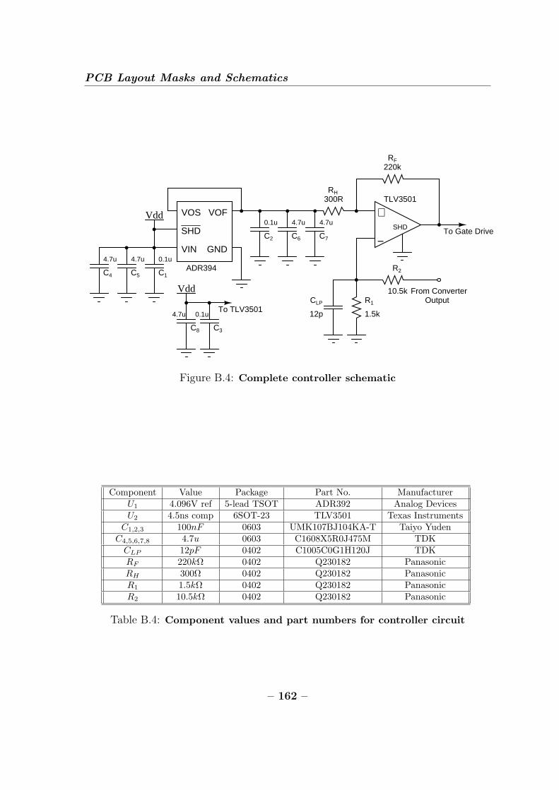
PCB Layout Masks and Schematics
−
+
SHD
VOS VOF
VIN GND
VddSHD
0.1u 4.7u4.7u
4.7u 4.7u 0.1u
220k
300R
10.5k
1.5k
ADR394
TLV3501
To Gate Drive
From ConverterR1
R2
RF
RH
CLP
12p
OutputVdd
4.7u 0.1uTo TLV3501
C1
C3
C2 C6 C7
C8
C5C4
Figure B.4: Complete controller schematic
Component Value Package Part No. ManufacturerU1 4.096V ref 5-lead TSOT ADR392 Analog DevicesU2 4.5ns comp 6SOT-23 TLV3501 Texas Instruments
C1,2,3 100nF 0603 UMK107BJ104KA-T Taiyo YudenC4,5,6,7,8 4.7u 0603 C1608X5R0J475M TDK
CLP 12pF 0402 C1005C0G1H120J TDKRF 220kΩ 0402 Q230182 PanasonicRH 300Ω 0402 Q230182 PanasonicR1 1.5kΩ 0402 Q230182 PanasonicR2 10.5kΩ 0402 Q230182 Panasonic
Table B.4: Component values and part numbers for controller circuit
– 162 –

(a) ST Top copper
(b) ST Bottom copper
(c) ST Top silkscreen
Figure B.5: ST board layout masks– 163 –

PCB Layout Masks and Schematics
(a) ST bottom silkscreen
(b) ST Route2
(c) ST Route3
Figure B.6: ST board layout masks– 164 –

(a) BCD Top copper
(b) BCD Bottom copper
(c) BCD Top silkscreen
Figure B.7: BCD board layout masks
– 165 –

PCB Layout Masks and Schematics
(a) BCD Bottom silkscreen
(b) BCD Route2
(c) BCD Route3
Figure B.8: BCD board layout masks
– 166 –

Bibliography
[1] J.G. Kassakian, M.F. Schlecht, and G.C. Verghese.Principles of Power Electronics. (Addison-Wesley), NY, 1991.
[2] Joshua W. Phinney. Multi-resonant Passive Components for Power Conver-sion. Ph.D. Thesis, Dept. of Electrical Engineering and Computer Science, Mas-sachusetts Institute of Technology, Cambridge, MA., June 2005.
[3] Francis Grover. Inductance Calculations. New York: Dover, 1946.
[4] Improved Calculation of Core Loss with Nonsinusoidal Waveforms, 4 Oct 2001.
[5] Duncan A. Grant and John Gowar. Power Mosfets: Theory and Applications.John Wiley & Sons, 1989.
[6] Joshua W. Phinney. Filters with active tuning for power applications. Master’sthesis, Massachusetts Institute of Technology, 2001.
[7] N.O. Sokal and A.D. Sokal. Class E—a new class of high-efficiency tuned single-ended switching power amplifiers. IEEE Journal of Solid-State Circuits, SC-10(3):168–176, June 1975.
[8] Nathan O. Sokal. Class-E RF Power Amplifiers. QEX, pages 9–20, Jan/Feb2001.
[9] R. Redl and N.O. Sokal. A new class-e dc/dc converter family with reduced partscount: Derivation, topologies, and design considerations. In Technical Papers ofthe Fourth International High Frequency Power Conversion Conference, pages395–415, 1989.
[10] R. Redl and N.O. Sokal. A 14 MHz 100 Watt class E resonant converter: Prin-ciples, design considerations, and measured performance. In 17th Annual IEEEPower Electronics Specialists Conference Proceedings, pages 68–77, June 1986.
[11] R.J. Gutmann. Application of RF circuit design principles to distributed powerconverters. IEEE Transactions on Industrial Electronics and Control Instrumen-tation, IEC127(3):156–164, 1980.
– 167 –

BIBLIOGRAPHY
[12] M. Iwadare, S. Mori, and K. Ikeda. Even harmonic resonant class e tuned poweramplifier without rf choke. In Electronics and Communications in Japan, vol-ume 79, pages 23–30, Jan. 1996.
[13] J.J. Jozwik and M.K. Kazimierczuk. Analysis and design of class-edc/dc con-verter. Industrial Electronics, IEEE Transactions on, 37(2):173–183, April 1990.
[14] H. Koizumi, Iwadare M., and Mori S. Class e2 dc/dc converter with secondharmonic resonant class e inverter and class e rectifier. In Thirs Annual AppliedPower Electronics Conference Proceedings, pages 1012–1018, 1994.
[15] H. Koizumi, H. Sekiya, M. Matsuo, S. Mori, and I. Sasae. Resonant dc/dcconverter with class de inverter and class e rectifier using thinned-out method(deleting some of the pulses to the rectifier). Circuits and Systems I: FundamentalTheory and Applications, IEEE Transactions on [see also Circuits and SystemsI: Regular Papers, IEEE Transactions on], 48(1):123–126, Jan. 2001.
[16] Michael J. Chudobiak. The use or parasitic nonlinear capacitors in class e am-plifiers. IEEE Transactions on Circuits and Systems I: Fundamental Theory andApplications, 41(12):941–944, December 1994.
[17] J.M. Rivas, J. Shafran, R.S. Wahby, and D.J. Perreault. New architectures forradio-frequency dc/dc power conversion. In 35th Annual IEEE Power ElectronicsSpecialists Conference Proceedings, pages 4074–4084, June 2004.
[18] J.M. Rivas, R.S. Wahby, J.S. Shafran, and D.J. Perreault. New architecturesfor radio-frequency dc/dc power conversion. In Power Electronics SpecialistsConference, 2004. PESC 04. 2004 IEEE 35th Annual, volume 5, pages 4074–4084Vol.5, 20-25 June 2004.
[19] Juan M. Rivas. Radio Frequency dc-dc Power Conversion. PhD thesis, Mas-sachusetts Institute of Technology, September 2006.
[20] Thomas H. Lee. The Design of CMOS Radio-Frequency Integrated Circuits.(Cambridge University Press), Cambridge, UK, second edition edition, 2004.
[21] T.H. Lee. Planar Microwave Engineering. (Cambridge University Press), 2004.
[22] F.H. Raab. Maximum efficiency and output of class-f power amplifiers. Mi-crowave Theory and Techniques, IEEE Transactions on, 49(6):1162–1166, June2001.
[23] F.H. Raab. Class-f power amplifiers with maximally flat waveforms. MicrowaveTheory and Techniques, IEEE Transactions on, 45(11):2007–2012, Nov. 1997.
– 168 –

BIBLIOGRAPHY
[24] J.W. Phinney, D.J. Perreault, and J.H. Lang. Radio-frequency inverters withtransmission-line input networks. In Power Electronics Specialists Conference,2006. PESC ’06. 37th IEEE, pages 1–9, 18-22 June 2006.
[25] David C. Hamill. Class DE inverters and rectifiers for DC-DC conversion. In27th Annual IEEE Power Electronics Specialists Conference Proceedings, pages854–860, June 1996.
[26] David A. Jackson. Design and characterization of a radio-frequency dc/dc powerconverter. M. Eng., Dept. of Electrical Engineering and Computer Science, Mas-sachusetts Institute of Technology, Cambridge, MA., June 2005.
[27] M.K. Kazimierczuk, B. Tomescu, and A. Ivascu. Class e resonant rectifier with aseries capacitor. Circuits and Systems I: Fundamental Theory and Applications,IEEE Transactions on [see also Circuits and Systems I: Regular Papers, IEEETransactions on], 41(12):885–890, Dec. 1994.
[28] W.A. Nitz, W.C. Bowman, F.T. Dickens, F.M. Magalhaes, W. Strauss, W.B.Suiter, and N.G. Zeisse. A new family of resonant rectifier circuits for highfrequency DC-DC converter applications. In Third Annual Applied Power Elec-tronics Conference Proceedings, pages 12–22, 1988.
[29] M.S. Nakhla and J. Vlach. A piecewise harmonic balance technique for determi-nation of periodic response of nonlinear systems. IEEE Transactions on PowerElectronics, CAS-23, No.2:85–91, 1976.
[30] J.M. Rivas, D. Jackson, O. Leitermann, A.D. Sagneri, Yehui Han, and D.J.Perreault. Design considerations for very high frequency dc-dc converters. InPower Electronics Specialists Conference, 2006. PESC ’06. 37th IEEE, pages1–11, 18-22 June 2006.
[31] D. J. Perreault. Evaluation of MOS Transistors for Very High Frequency PowerConversion. Internal Memorandum, Laboratory for Electromagnetic and Elec-tronic Systems, Massachusetts Institute of Technology, June 2005.
[32] James Warren, III. Cell-modulated resonant dc/dc power converter. M. Eng.Thesis, Dept. of Electrical Engineering and Computer Science, MassachusettsInstitute of Technology, Cambridge, MA., August 2005.
– 169 –