design of a smart push pull inverter coupled with
TRANSCRIPT

MANSOURA ENGINEERING JOURNAL, (MEJ), VOL. 41, ISSUE 2, JUNE 2016 E: 11
Mansoura University
Faculty of Engineering
Mansoura Engineering Journal
Abstract—Although the photovoltaic (PV) system plays an
important role to meet our needs of an electrical energy, it
represents a direct current (DC) source. So, it is not suitable for
alternating current (AC) residential loads. This paper proposes a
design and practical implementation for a smart single phase low
cost inverter, which could be an effective solution to reduce the
overall cost of the PV system and supply AC loads. The low cost
inverter is achieved by designing low cost control and power
circuits. In the power circuit, PV modules operate near the
maximum power point (MPP) and supply AC load requirements
through the inverter switches. The control circuit uses a
microcontroller which provides a smart system for interaction
with the user and remote control and monitoring, in addition to
use a digital control to maintain the AC output voltage at the
required value.
1. INTRODUCTION
here are two general types of inverters: current
source inverter and voltage source inverter. The
voltage source inverter has a fixed input voltage
and is more popular and widely applied in photovoltaic, wind
power generation, and other forms of renewable power
Received: 31 March, 2016 - revised: 13 April, 2016 – accepted: 23 May,
2016
Eid Gouda, Electrical engineering department, Mansoura University. (E-mail: [email protected])
Ahmed Abdelhaleim, Electrical engineering department, Mansoura
University. (E-mail: [email protected]) S. S. Eskander, Electrical engineering department, Mansoura University
generation. For the voltage-source inverter whose input
voltage is fixed, its output voltage level can be controlled [1]-[4].
Single-phase voltage-source inverters can be built in the
following three topologies. Firstly, the half bridge inverters
consists of two large capacitors are required to provide a
neutral point, such that each capacitor maintains a constant
voltage which equals to half of input DC voltage. So a set of
large capacitors is required [5]-[7]. Secondly, Full bridge (H-
bridge) inverter is similar to the half-bridge inverter; however,
a second leg provides the neutral point to the load [8] - [10].
Thirdly, a Push-pull inverter consists of only two switches and
three terminal power transformers. The cost of the push pull
inverter depends only on the two power electronics switches,
instead of four switches in single phase full bridge inverter,
where each switch requires driver circuit, and control signal,
and protection circuit. Also, the other main component in the
push pull inverter is its transformer which is similar to the
transformer of full bridge inverter except that the push pull
transformer has two primary windings with half of the rating
of the primary winding in full bridge inverter [11]-[16].
The simplest switching scheme for the push pull converter
produces a square wave output voltage. The periodic
switching of the load voltage between +Vdc and -Vdc
produces a square wave voltage across the load. Although this
alternating output is non-sinusoidal, it may be an adequate AC
waveform for some applications. On other hand, Pulse Width
Design of a Smart Push Pull Inverter Coupled
with Photovoltaic System
عاكس كھربي ذكي موصل لمنظومة ذیو تنف میتصم
ةیفوتوفولت Eid Gouda, Ahmed Abdelhaleim, S. S. Eskander
KEYWORDS:
Inverter,
Microcontroller, MPP
and Smart System
إن منظومة الطاقة الفوتوفولتية هي مصدر من مصادر الطاقة النظيفة المتجدده لتوليد -:الملخص العربي
الطاقة الكهربية في العصر الحالي. في هذه المنظومة يتم إستخدم عاكس كهربي لتحويل التيار المستمر إلي
مة. يقترح هذا البحث من التكلفة الاجمالية للمنظو % 05التيار المتردد. تصل تكلفه هذا العاكس الكهربي إلي
تصميم عاكس كهربي بأقل تكلفة و أعلي إعتمادية و بطريقة مبسطة. تم تصميم هذا العاكس الكهربي من النوع
Push Pull بإستخدام المتحكمات الدقيقة و القابلة للبرمجة مما يجعله يعطي خرج قابل للتعديل و التغير طبقا
ية. كما تم إستخدام دوائر عزل ضوئي بين دائرة تغذية الحمل من للمتطلبات الحمل و المنظومة الفوتوفولت
البطارية و دائرة التحكم المرتبطة بدوائر المتحكمات الدقيقة مما يعطي أداء أكثر إستقرارا و تحكم أفضل
لوبة لدائرة التغذية. بالاضافة لقدرة هذا العاكس الكهربي علي المحافظة علي قيمة جهد الخرج عند القيمة المط
بواسطة المستخدم. يحتوي هذا العاكس الكهربي علي دوائر حماية للعاكس الكهربي نفسة و للحمل بالإضافة
لإمكانية المراقبة و التحكم في العاكس عن بعد في الانظمة الكهربية الذكية.
T

E: 12 EID GOUDA, AHMED ABDELHALEIM AND S. S. ESKANDER
Modulation (PWM) control scheme is complex, but its output
can become sinusoidal with small filters [17] – [21].
The main goal of this paper is to design and implement a
smart push pull inverter for PV supplied homes. It’s known
that the lighting loads, fans, refrigerator and water pump
represent the main different types of domestic loads. Table 1
contains the active power rating and the power factor for each
load. These loads operate on 220V, 50Hz AC power system.
Also the total apparent power is calculated for all the loads to
calculate rating of different components in PV power system.
This table shows that the total load on the system is 2356 VA.
Therefore, this paper discusses the design of a system with
rating 2500 VA.
This paper is divided into 5 main sections. An introduction
was represented in section 1.The design steps of each
component of the proposed inverter such as the used batteries,
switches, transformer, power supply circuit, gate driver circuit,
protection circuits will be shown in section 2 in detail. The
inverter control system, microcontroller coding and remote
interactive control system will be located in section 3.The
most important section of this paper will be found in sections
4, 5 and 6 where the implementation of the inverter, result
discussion and remote monitoring of the control system will
be analyzed. Finally a conclusion will be presented in section
7. TABLE 1
THE LOADS TO BE SUPPLIED BY THE DESIGNED PV SYSTEM [22]
Load Type Active
Power
Rating (W)
Power factor
𝐜𝐨𝐬 𝝋
Apparent
Power (VA)
Refrigerator 800 0.65 1231
Fan 65 0.7 93
Tube Light 50 0.5 100
Water Pump 745 0.8 932
Total Load 1660 2356
2. INVERTER DESIGN
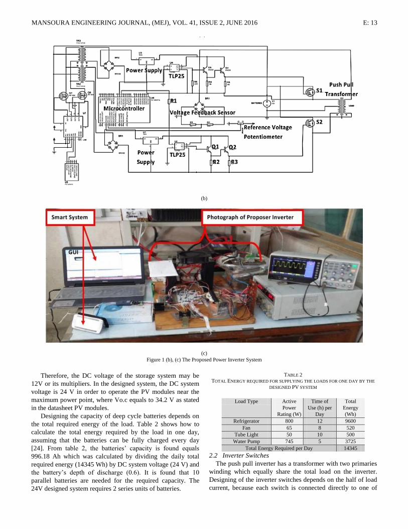
Figure 1(a) shows the block diagram of the proposed power
inverter within the PV system. The design of the inverter
circuits will include sizing the DC batteries or the DC voltage
system. Then, the choosing of suitable semiconductor switches
for the inverter will be discussed. And, the power transformer
will be designed. Also, the design of a gate driver circuits for
the inverter switches and their power supply circuits are
discussed. Moreover, the design of protection devices for the
inverter system is included. The schematic diagram of this
inverter system is shown in figure 1(b). And, figure 1(c)
shows a photograph for the final connection of the different
components in the designed inverter.
2.1. DC Batteries
A battery is a storage vessel for electricity. Deep cycle
batteries are the key component in various types of renewable
energy systems that require the storage of electricity. A deep
cycle battery is designed to discharge between 45% and 75%
of its capacity, depending on the manufacturer and the
construction of the battery. The mean value
60% depth of discharge can be used in sizing of DC
batteries required for the load. In the market, these batteries
usually have the following specifications: 12V, and 100Ah
[23].
Figure 1 (a) The Proposed Power Inverter System
MANSOURA ENGINEERING JOURNAL, (MEJ), VOL. 41, ISSUE 2, JUNE 2016 E: 13
(b)
(c) Figure 1 (b), (c) The Proposed Power Inverter System
Therefore, the DC voltage of the storage system may be
12V or its multipliers. In the designed system, the DC system
voltage is 24 V in order to operate the PV modules near the
maximum power point, where Vo.c equals to 34.2 V as stated
in the datasheet PV modules.
Designing the capacity of deep cycle batteries depends on
the total required energy of the load. Table 2 shows how to
calculate the total energy required by the load in one day,
assuming that the batteries can be fully charged every day
[24]. From table 2, the batteries’ capacity is found equals
996.18 Ah which was calculated by dividing the daily total
required energy (14345 Wh) by DC system voltage (24 V) and
the battery’s depth of discharge (0.6). It is found that 10
parallel batteries are needed for the required capacity. The
24V designed system requires 2 series units of batteries.
TABLE 2 TOTAL ENERGY REQUIRED FOR SUPPLYING THE LOADS FOR ONE DAY BY THE
DESIGNED PV SYSTEM
Load Type Active
Power
Rating (W)
Time of
Use (h) per
Day
Total
Energy
(Wh)
Refrigerator 800 12 9600
Fan 65 8 520
Tube Light 50 10 500
Water Pump 745 5 3725
Total Energy Required per Day 14345
2.2 Inverter Switches
The push pull inverter has a transformer with two primaries
winding which equally share the total load on the inverter.
Designing of the inverter switches depends on the half of load
current, because each switch is connected directly to one of

E: 14 EID GOUDA, AHMED ABDELHALEIM AND S. S. ESKANDER
the primary windings of the transformer. The load current can
be calculated from equation (1).
I= 0.5 * (load rating/DC System Voltage) =
2500
(2∗24)= 52.1 𝐴 (1)
The IGBT switches are used in this paper, because IGBT
switches have higher power capabilities up to 1700 kVA, 2000
V, 800 A than the power capabilities of MOSFETs. Also, the
heating losses of the IGBT are lower because of its lower
resistance than the MOSFET. Their forward voltage drop is 2-
3 V. Moreover, this type of switches can withstand the
overloading and operates in parallel well due to the negative
temperature coefficient. In addition, they have relatively
simple voltage controlled gate driver and low gate current.
[25], [26].
2.3 Transformer
Figure 1(b) shows the transformer which can be used in
push-pull inverter. The primary winding of transformer has the
following voltage ratings: 24-0-24 volt. And the voltage rating
of the transformer’s secondary terminals are 0-260 volt to
allow accessing 220V at the output of the inverter during the
different loading conditions. The power rating of the
transformer is 2500VA [27]. The open circuit test and short
circuit test for the transformer were carried out experimentally
in order to get the impedances of transformer equivalent
circuit. It is found from tests that 𝑥𝑚 = 4.235 𝛺 Rfe =
15.5 Ω rt = 0. 0143Ω, and xlt = x_lt= 0.007Ω.
2.4 Power supply Circuit
Figure 1(b) displays the schematic diagram of power
supply circuit. This circuit is used to convert the 24 V of the
DC batteries into 5 V for supplying the microcontroller. Also,
it converts the 24 V into 15 V for the gate driver circuit for the
IGBT switches. It consists of voltage regulator, diode, and
smoothing capacitor in the output. Designing of the smoothing
capacitor depends on the maximum voltage ripple which can
occur due to a load on the power supply. The maximum load
current on this power supply circuit is the current of driver
circuit which reaches to 500 mA during the ON time of the
switches. The smoothing capacitor will supply this maximum
current by only 10% of its amount charge (Q = CV) in order to
achieve fast charging and discharging of capacitor and
maintain the output voltage constant. Therefore the
capacitance will equal to 2000 uF . It is found that the total
cost of all components in power circuit of the proposed
inverter is nearly $600 where the exact costs are in the
Appendix.
2.5 Gate Driver circuit
In the proposed inverter, the driver circuit depends mainly
on TLP250 integrated circuit. This integrated circuit is an
optically isolated driver, meaning that the input and output are
optically isolated. The TLP250 has an input stage, an output
stage and a power supply connection. Table 3 shows the status
of the two output transistors depending on the LED in the
input stage.
TABLE 3
TLP250 TRUTH TABLE
TR1 TR2
Input LED ON ON OFF
OFF OFF ON
Figure 1(b) shows the schematic diagram for TLP250
driver circuit which is proposed in this paper. Firstly,
designing the input stage of TLP250, the input stage consists
of LED. LED has an input forward voltage (1.6V) and a peak
forward current (10mA). Therefore, R1 will equal 320Ω.
From datasheet of the optocoupler, the maximum collector
current of output transistors is 7 mA. Therefore, two
transistors Q1, Q2 are required to protect the opotocoupler.
Firstly, from the maximum collector current of
phototransistors and ohm’s law, resistance R2 will equal
2142.86 Ω. The nearest standard value resistance equals
2.2KΩ, and its power rating must be more than (14mA)2 ∗
2.2 ∗ 103 = 0.4312 watt Providing adequate current for the gate of the IGBT
switches entails that the transistor Q2 should be saturated. It is
found R3 equals 270 Ω as standard value. The power rating
for R3 must be greater than (100mA)2 ∗ 270 = 2.7 watt. The TLP250, being an optically isolated driver, has
relatively slow propagation delays. The propagation delay
time will typically lie between 0.15µs and 0.5µs. The
datasheet specifies the maximum operating frequency to be 25
kHz. Therefore, it is suitable for the proposed inverter in this
paper, in which the TLP250 is used for frequencies up to
about 50 Hz in square wave operation.
A 0.1µF bypass capacitor should be connected between pin
8 and pin 5. This capacitor stabilizes the operation of the high
gain linear amplifier in the TLP250. Failure to provide this
capacitor may impair the switching property. The capacitor
should be placed as close to the TLP250 as possible. Added
100µF is for smoothing, as a bulk capacitor.
2.6 Over Current Protection (Fuses and Circuit Breaker)
Over current protection is used in both the power and
control circuits. Firstly, in control circuit, there are 0.1A fuses
to protect the driver circuits of the IGBT and microcontroller
circuits. Also, a power fuse with rating 40A in addition to
circuit breaker 63A are used to protect the power circuit of the
inverters.
2.7 Snubber Protection Circuits
Snubber circuit is a supplementary circuit used in the
converter circuit to reduce stress put on the power
semiconductor device. The ultimate goal of the snubber circuit
is to improve the transient waveform. The snubber circuit
suppresses over-current or over-voltage. The most common
reasons for using a snubber are to limit the peak voltage across
the inverter semiconductor switch and to reduce the switching

MANSOURA ENGINEERING JOURNAL, (MEJ), VOL. 41, ISSUE 2, JUNE 2016 E: 15
loss during turn-off. The snubber circuit has many
configurations. The simplest snubber circuit for IGBT in
inverter applications is RC snubber circuit [28]. Designing of
snubber circuit for IGBT switches can be calculated from the
following approximate method [29].
A. - The resistance value is chosen to allow the flow of load
current without voltage overshoot after the switch opens.
The resistance value calculated from equation (2)
depending on Vo and I. Vo is off voltage across the switch
after it opens and I is on current before the switch opens.
𝑅 ≤ 𝑉𝑜
𝐼 ≤
24
42 ≤ 0.57 (2)
B. - The resistance will dissipate the energy stored in the
snubber capacitor, ½*Cs∗ Vo2, for each voltage
transition regardless of the resistance. The capacitance will
be chosen to cause the 7-watt resistor to dissipate half of
its power rating, 3.5 watts. For two times fs (switching
frequency= 1000 HZ) transitions per second, the resistor
will dissipate 3.5 watt. Then, Cs can be calculated from
equation (3).
𝐶𝑠 =3.5
𝑓𝑠 𝑉𝑜2 = 6 µF (3)
3. INVERTER CONTROL SYSTEM
The control system of the inverter depends mainly on a
microcontroller. Also, there is a connection between the
microcontroller and A Personal Computer (PC) which plays a
great role in smart systems. This connection allows the user to
remote control and monitor for the overall performance of the
system in two ways. Firstly, the user can monitor and control
the inverter by using a simple Graphical User Interface (GUI)
on the PC. Secondly, sending and receiving standard e-mails
between the user and the inverter system. This allows the user
to know and control the status of the system from any PC or
phone. The total cost of control circuit of the proposed inverter
is about $ 20 where the exact costs are in the Appendix.
3. 1. Microcontroller Coding
PIC microcontroller will be programmed to generate the
control signals for inverter switches S_1, and S_2 shown in
figure 1(b). These control signals are responsible for
converting the DC voltage of batteries into 50 HZ AC voltage.
Also, changing the duty cycle of the control signal will change
the RMS value of output AC voltage from the inverter.
Figure 1(b) shows schematic diagram of microcontroller
circuit. Two analogue inputs are used. One of them is used to
measure the reference value of AC output voltage. The
second is used to measure a value of actual AC voltage. Then,
microcontroller compares
Both values of analogue inputs to give proper control
signals.
The program of microcontroller should consider the dead
time for the inverter switches. This dead time depends on the
inductance of the load. The current i of an inductive load
continue after the termination of the load voltage by
conduction angle β this angle (β) will be calculated firstly.
Based on this conduction angle and reference voltage input for
the microcontroller, the output control signals will be
generated by the microcontroller.
Control signal for the square wave inverter consists of two
time periods in each half cycle. In each half cycle, the inverter
switch (S1, or S2) is closed during. Ton milliseconds and is
open during Toff milliseconds. Toff for the inverter switches
must equal to or greater than the dead time for this load. The
dead time is calculated from the conduction angle β. Then, the
calculation of Toff will depend on dead time, reference
voltage, and actual output voltage. Therefore, in
microcontroller code, there is minimum value for Toff This
minimum value equals to the calculated the dead time for the
load. So the flowchart for the microcontroller code should be
as figure 2.
A. Fuzzy Logic Voltage Stabilization Control Loop
The calculation of Toff for the inverter switches depends
on a simple fuzzy logic equation (4).
𝑇𝑜𝑓𝑓 =𝑉𝑜𝑢𝑡−𝑉𝑟𝑒𝑓
𝑉𝑟𝑒𝑓∗ 10𝑚𝑠 + 𝑇𝑜𝑓𝑓 (4)
In equation (4), Toff is calculated based on the initial value
for Toff which equal to the calculated dead time for the
load at the beginning of inverter operation. Then, during
the operation of inverter, Toff increases when the output
voltage becomes larger than the reference voltage. On the
other hand, Toff decreases based on the percentage error
between the output voltage and the reference voltage when
the output voltage becomes less than the reference voltage.
The maximum value for Toff is 10 ms which is the half of a
switching period for 50 Hz output.
B. Calculation of Load Conduction Angle
Calculation of load conduction angle requires knowing
the total impedance seen by the inverter switches. So,
firstly, the total impedance of transformer and the load will
be calculated. Then, from the current equation of the load,
the conduction angle can be calculated. Table 4 shows the
calculation of loads impedances and the total load
impedance and impedance referred to 24 V side of the
transformer. The total impedance (Z⌊φ) on the inverter can
be calculated which is equal to 0.255 ⌊47.2°
The conduction angle angle β is calculated from the
load current (equation 5) and its value equal 3.93 radian.
The dead time equals 2.5 ms which is calculated by
equation (6).
𝑖 = √2∗𝑉∗𝑠𝑖𝑛 (𝑤𝑡−𝜑)
𝑍+
√2∗𝑉∗𝑠𝑖𝑛 𝜑
𝑍𝑒−
𝑅
𝐿𝑡 (5)
Dead time = (𝛽 − 𝜋) ∗10 𝑚𝑠
𝜋= 2.5 𝑚𝑠 (6)

E: 16 EID GOUDA, AHMED ABDELHALEIM AND S. S. ESKANDER
Figure 2 Software Flowchart
3. 2. Remote Interactive Control System
The Universal Asynchronous Receiver Transmitter
(UART) module is the basic serial I/O module available in the
microcontroller.
The UART is a full duplex asynchronous system that can
communicate with peripheral devices, like personal
computers, RS-232, and RS-485 interfaces [29]. The DC
batteries voltages, its state of charge, the inverter’s output
voltage, system state of operation are transmitted from
microcontroller to the PC via the UART module. The
microcontroller sends this information through its UART
module at rate 9600 bps and its logic voltage 0-5 V.
TABLE 4
CALCULATION OF TOTAL LOAD IMPEDANCE
Load Type Rating
(W)
Power factor
(cos 𝜑)
I(A) |𝐼|(A) 𝑍(Ω)
Refrigerator 800 0.65 3.64-j4.25 5.59 25.56+j29.88
Fan 65 0.7 2.05-j2.73 3.41 364.9+j372.2
Tube Light 50 0.5 0.23-j0.394 0.45 242+j419
Water Pump 745 0.8 3.38-j2.5 4.2 41.6+j31.18
Total Impedance of Load in Parallel (𝑍𝐿′) 14.72 +j15.573
ZL = ZL′* (24/220)2 0.1752+j0.18533
Then, the RS232 circuit is used to convert the 0-5 V signal
from the microcontroller into 0-12 V logic signal which can be
read by the PC. By using the serial to USB converter, this
microcontroller system can be connected to any PC. Finaly,
The PC displays all the information for the user though a GUI
which shown in figure 1(c). Also, PC sends an e-mail which
contains this displayed information upon the user’s request.
4. IMPLEMENTATION
The implementation of the proposed inverter includes the
following steps:
A. All designed circuits for the inverter are implemented on
Printed Circuit Board (PCB) by using PROTEUS DESIGN
SUITE program. Figure 3 shows PCB of microcontroller
control circuit.
Start
Modify output control
signals for IGBT
switches
)tage(Output vol
),( Voltage Reference Read
V
V
out
ref
)4.(EqfromCalculate T off
timeDeadT off
NO
YES
NO
YESmsT off
10
timeDeadSet T OFF
If
If
TimeDeadSet T OFF
mSSet T OFF10
TT OFFONmSSet 10

MANSOURA ENGINEERING JOURNAL, (MEJ), VOL. 41, ISSUE 2, JUNE 2016 E: 17
B. 16F877A is used as a microcontroller in the designed
system. Because PIC microcontroller require 4 clock
cycles for each instruction cycle, an external oscillator
circuits for microcontroller can be 4 MHZ. It is adequate to
generate control signal at frequency 50 HZ. This
microcontroller is programmed by using MikroC.
C. In order to avoid the saturation of the power transformer,
polarity test is conducted to find which terminals of the
primary windings will be connected to the same point. And
the other terminals are connected to the inverter switches.
D. Two inverter switches are placed in two separate heat
sinks. Heat sinks are close to each other in order to be
cooled with one fan.
E. In the designed system, 16 mm^2 cables are used in power
circuit. And 0.3 mm^2connecting wires are used in
control circuits.
F. Crocodile clamps prepared to easily connect DC batteries
with inverter.
G. RS232 converter module and USB to (RS-232/RS232)
Serial port (male connector) device are used to connect the
inverter to the PC. And the PC program is implemented
though Microsoft Visual Studio environment by using C#
programming language.
5. RESULTS AND DISCUSSIONS
The operation of the proposed system is discussed in the
following three sections. The first section discusses the
modeling of the inverter. Then, the proposed control system is
achieved in practical implementation through using the square
wave control in the second section and Pulse Width
Modulation (PWM) control for inverter switches is presented
in the last section.
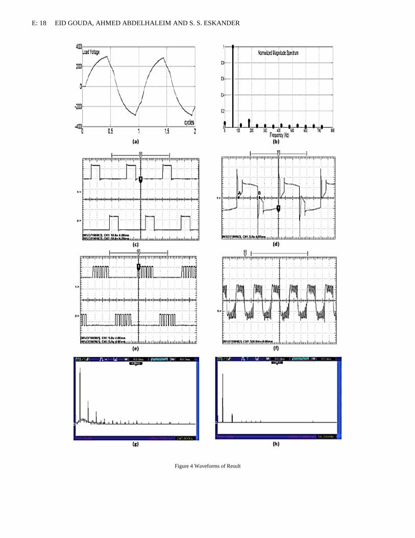
5.1. Results of Inverter State Space Model
The simulation for inverter output under the proposed
control system is investigated by using state space modeling
for the proposed inverter. This modeling is solved by using
MATLAB and gives the output voltage shown in figure 4(a).
The harmonic spectrum for the modeling output voltage is also
calculated and plotted in figure 4(b). This spectrum shows that
there is no requirement for using a filter.
5.2. Results of Square Wave Control for Inverter Switches
For square wave control, the output signals from the driver
circuit is shown in figure 4(c) which takes the same shape of
the control signals from microcontroller. Figure 4(d) shows
the output of the inverter with full load and 220 V on the
output. These outputs waveform is measured by using scale of
38:1. In figure 4(d), points A, B is the limits of one half cycle
of the output voltage waveform. The voltage near to points A
and B falls to zero, because it represents the calculated Toff of
the control signal. Also, it can be noted that the output near
point A and B is not still zero during. Toff . Near to points A
and B, the output voltage is greatly deviate from the sinusoidal
shape and largely increase during Toff due to the fast change
in the state of power circuit of inverter. This fast change in
output voltage can damage the electrical equipment connected
to this system. This output voltage can be investigated also
from analyzing its harmonic spectrum. Figure 4(g) displays
the harmonics magnitude spectrum for output voltage during
220V output voltage with full load. This harmonics magnitude
spectrum shows an increase in harmonics more than the
expected value from the modeling results. Therefore, it is
necessary to use large filters which can eliminate these
harmonics.
5.3. Results of PWM Control for Inverter Switches
The constant square wave control signal for the inverter
switches can be divided into pulses with small width. These
pulses are generated according to a comparison between 1KHz
triangular wave and 50Hz sinusoidal wave (PWM unipolar
switching scheme). The generated control signals for both
switches of inverter are shown in figure 4(e). Moreover, it
should be note that the snubber capacitor in PWM control
should be less than 5 µF. Figure 4(f) shows the resulted AC
output from the inverter. This output is close to sinusoidal
shape more than the square wave control. Therefore, the
harmonic spectrum for this output voltage (as figure 4(h))
contains fewer harmonics which allow all the electrical
equipment in the system, either the inverter itself or the loads
connected to the inverter, to provide better performance.
6. RESULTS OF REMOTE MONITORING AND CONTROL
SYSTEM
The GUI of the remote monitoring and control system
prepared by Microsoft Visual Studio is displayed in figure 1(c)
which also shows the standard e-mail sent from the system to
the user. The implementation of this monitoring and control
system depends mainly on the UART module in
microcontroller. This module sends all system data and
receives control commands to/from the personal computer.
Figure 3 PCB of control circuit
E: 18 EID GOUDA, AHMED ABDELHALEIM AND S. S. ESKANDER
Figure 4 Waveforms of Result

MANSOURA ENGINEERING JOURNAL, (MEJ), VOL. 41, ISSUE 2, JUNE 2016 E: 19
7. CONCLUSION
Design and implementation of economical smart push pull
inverter are presented in details in this paper. The total cost of
2.5 Kw inverters in [31] reaches up to $1800. So the cost of
the proposed inverter reduced by more than 50%. The scheme
implementation at low cost was demonstrated. The paper
provides impressive results based on the comparison between
the practical results and results of the state space modeling of
the system. Moreover, this inverter can be used in smart
systems depending on its capabilities to contact with the user
either by GUI or e-mail. A visual environment is included in
the designed system to facilitate its monitoring and control.
Finally, this system achieves a simple method to operate the
PV modules near its maximum power point
8. REFERENCES [1] Teraya,D., Masukawa, S. and Iida, S. “Inverter for Interchangeable Use
as Current Source Inverter and Voltage Source,” Electrical Engineering in
Japan, Vol. 183, No. 4, 2013.
[2] Lidozzi, A., Solero, L., Bifaretti, S., and Crescimbini, F. "Sinusoidal Voltage Shaping of Inverter-Equipped Stand-Alone Generating Units,"
IEEE Transactions on Industrial Electronics, Vol. 62 , Iss. 6, pp. 3557-
3568, June 2015 [3] Jithesh, M., and Prawin, A. “Design and Analysis of a Single Phase
Unipolar Inverter Using Sliding Mode Control,” International Journal of
Engineering and Advanced Technology (IJEAT), Vol. 2, Issue 2, 2012 [4] Adhikari, N., Singh, B., Vyas, A., Chandra, A., and Al-Haddad, K.
“Analysis and design of isolated solar-PV energy generating system,”
IEEE Annual Meeting on IAS, pp. 1 – 6, 2011. [5] Chan, C. K., Cheng, K. W. E., and Ho, S. L. "Half-bridge converter based
on switched-capacitor resonance without using deadtime control for
automotive applications," IET Power Electronics, Vol.4, Iss 6, pp. 657-662, July 2011
[6] Fazeli, M., Ekanayake, J. B., Holland, P. M., and Igic, P. "Exploiting PV
Inverters to Support Local Voltage—A Small-Signal Model," IEEE Transactions on Energy Conversion, Vol.29, Iss. 2, pp. 453-462, June
2014
[7] Dalci, K., Gulez, K., and Cansever, G. “The design of a push-pull switch mode power supply for AC drives,” IEEE Annual Conference on IECON
of, Vol. 2, pp. 1201 – 1206, 2004
[8] Kapadia, N., Patel, A., and Kapadia, D. “Simulation and Design of Low cost Single Phase Solar Inverter,” International Journal of Emerging
Technology and Advanced Engineering, Vol 2, Issue 1, February 2012
[9] Caixeiro Mattos, F., Lacerda, V. S., Valle, R. L., Ferreira, A.A., Barbosa, P. G., and Braga, H. A. C. "Contribution To The Study Of A Single-
Phase And Single Stage Photovoltaic System," IEEE Latin America
Transactions, Vol. 13, Iss. 5, pp. 1265-1271, May 2015 [10] Skvarenine, T. “The Power Electronics Handbook,” CRC PRESS, 2nd
edition, 2002
[11] Martino, M., Citro, C., Rouzbehi, K., and Rodriguez, P. “Efficiency Analysis of Single-Phase Photovoltaic Transformer-less Inverters,”
International Conference on Renewable Energies and Power Quality
(ICREPQ’12), 2012 [12] Hagiwara, M., and Akagi, H. "Experiment and Simulation of a Modular
Push–Pull PWM Converter for a Battery Energy Storage System," IEEE
Transactions on Industry Applications, Vol. 50, Iss. 2, pp. 1131-1140, April 2014
[13] Shema, S., Daut, I., Irwanto, M., Shatri, C., Syafawati, N., and Ashbahani, N. “Study of inverter design and topologies for photovoltaic
system,” IEEE Int. Conf. on INECCE , PP. 501 – 504, June 2011
[14] Otero-De-Leon, R., and Mohan, N. “A push-pull DC-AC high frequency power electronics transformer for photovoltaic applications,” IEEE
Conference on Industrial Electronics Society, pp. 1131 – 1136, 2014
[15] Jianqiang, W., Jingxin, L. and Weige, Z. “Interleaved push-pull converter with very low input and high output,” IEEE Int. Conf. on PEITS, Vol. 3,
pp. 247 – 249, 2009
[16] Shungang, X. “Design of photovoltaic high frequency link inverter based on push-pull forward converter,” IEEE Int. Conf. on ICCCAS, pp. 593 –
596, 2010
[17] Mukhtar, S. M., Saad, A., and Hanafi, N. “A high efficiency
microcontroller-based step-up push-pull DC-DC converter for PV inverter,” IEEE Int. Conf. on PECon, pp. 141 – 145, 2010
[18] Kushwaha, R., Saha, T. K., Barman, J. C. and Dey, J. "Analysis and
design of 2 DOF control of push-pull converter used for standalone PV system," IEEE Int. Conf. on Renewable Energy Congress (IREC), March
2015
[19] Yin, L., Zhao, Z., Lu, T., Yang, S., and Zou, G. "An Improved DC-Link Voltage Fast Control Scheme for a PWM Rectifier-Inverter System,"
IEEE Transactions on Industry Applications, Vol.50, Iss. 1, pp. 462-473,
Feb. 2014 [20] Wu, T., Wang, S., Kuo, C., and Lee, K. “Design and implementation of a
push-pull phase-shifted bi-directional inverter with a dsPIC controller,” IEEE Int. Conf. on PEDS, pp. 728 – 733, 2009
[21] Kim, Y. C., Jin, L., and Choi, J. “Direct Digital Control of Single-Phase
AC/DC PWM Converter System”, Journal of Power Electronics, Vol. 10, No. 5, September 2010
[22] Ramamurthy, G. “Handbook of Electrical Power Distribution,”
Universities Press, 1st Edition, 2004 [23] Linden, D., Reddy, T., “Handbook of Batteries 3rd Edition,” McGraw-
Hill, 3rd edition, 2002.
[24] Lynn, P. “Electricity from Sunlight: An Introduction to Photovoltaic,”
John Willy, 1st Edition, 2010.
[25] Schwarzer, U., and Doncker, D. “Design and implementation of a driver
board for a high power and high frequency IGBT inverter,” IEEE Int. Conf. on Power Electronics, Vol. 4, pp. 1907 – 1912, 2002
[26] Islam, M., and Mekhilef, S. “High efficiency transformerless MOSFET
inverter for grid-tied photovoltaic system,” IEEE Int. Conf. on APEC, 2014
[27] Hart, D. W. “Power Eelectronics,” McGraw-Hill Companies, 1st edition,
2010 [28] Chokhawala, R., and Sobhani, S. “Switching Voltage Transient
Protection Schemes for High-current IGBT Modules,” IEEE Trans.
Industry applications, vol. 31, no. 2, pp. 256-263, 2011 [29] Chitode, J. “Power Electronics” Technical Publication Pune, 3rd edition,
2008
[30] Lee, J., Chuah, Y., and Chai C. “A Multilevel Home Security System (MHSS),” International Journal of Smart Home, Vol. 7, No. 2, March,
2013.
[31] Mayer, J. N., Philipps S., Hussein, N. S., Schlegl, T., and Senkpiel, C. “Current and Future Cost of Photovoltaics Study,” Agora Energiewende,
February 2015.
APPENDIX: THE EXACT COSTS OF THE PROPOSED
INVERTER’S COMPONENTS
1- The Exact Costs of Power Circuit components
Item Price in US Dollar
Power transformer 250
IGBT switches and Heat Sinks 310
Connectors 7.5
Cables 4
Circuit Breaker and Fuses 10
Fans 4
Total 585.5
2- The Exact Costs of Control and Driver Circuit
Components
Item Price in US Dollar
Control Circuit Board 12
Volt Sensor 4
Control Circuit Board 7
Total 23