design of a highly linear 24-ghz lna - vtechworks.lib.vt.edu · emitter follower architecture, ......
TRANSCRIPT
Design of a Highly Linear 24-GHz LNA
Hedieh Elyasi
Thesis submitted to the faculty of the
Virginia Polytechnic Institute and State University
in partial fulfillment of the requirements for the degree of
Master of Science
In
Electrical Engineering
Dong S. Ha, Chair
Luke Lester
Sanjay Raman
April 26, 2016
Blacksburg, VA
Keywords: Highly linear, low power, wideband, 24-GHz LNA, peaking technique, gain
extension, buffer.
Copyright 2016, Hedieh Elyasi

ii
Design of a Highly Linear 24-GHz LNA
Hedieh Elyasi
(ABSTRACT)
The increasing demand for high data rate devices and many applications in short
range high speed communication, attract many RF IC designers to work on 24-GHz
transceiver design. The Federal Communication Commission (FCC) also dedicates the
unlicensed 24-GHz band for industrial, science, and medical applications to overcome
the interference in overcrowded communications and have higher output signal power.
LNA is the first building of the receiver and is a very critical building block for the
overall receiver performance. The total NF and sensitivity of the receiver mainly
depends on the LNA’s NF that mandates a very low NF LNA design. Depending on its
gain, the noise figure of the next stages can relax. However, the high gain of an LNA
enforces the next stages to be more linear since they suffer from larger signal at their
input stage and can get saturated easily. Apparently, designing high gain, low noise, and
highly linear LNA is very stimulating.
In this thesis, a wideband LNA with low noise figure and high linearity has been
designed in 8XP 0.13-µm SiGe BiCMOS IBM technology. The highlight of this design
is proposing the peaking technique, which results in considerable linearity
improvement. Loading the LNA with class AB amplifier, power gain experiences a
peaking in high input signal swing levels.
The next stager after the LNA is the buffer to provide isolation between the LNA and
mixer, and also avoid loading of the LNA from the mixer. Instead of using popular
emitter follower architecture, another circuit is proposed to have higher gain and
linearity. This buffer has two separate out of phase inputs, coming from the LNA and
are combined constructively at the output of the buffer.

iii
Since the frequency of this design is high, electromagnetic (EM) simulation for pads,
interconnects, transmission lines, inductors, and coplanar transmission lines has been
completed using Sonnet cad tool to consider all the parasitic and coupling effects.
Considering all the EM effects, the LNA has 15 dB gain with 2.9 dB NF and -8.8 dBm
input 1-dB compression point. The designed LNA is wideband, covering the frequency
range of 12-GHz to 31-GHz. However, the designed LNA, has the capability of having
higher gain at the expense of lower linearity and narrower frequency band using
different control voltage. As an example peak gain of 29.3 dB at the 3-dB frequency
range of 23.8 to 25.8-GHz can be achieved, having 2.3 dB noise figure and -17 dBm
linearity.

iv
Design of a Highly Linear 24-GHz LNA
Hedieh Elyasi
(ABSTRACT)
Nowadays, wireless devices like cell phones, remote controls, laptops, and modems
are becoming unavoidable part of human daily life. Increasing demand for having higher
speed and many applications in short distance such as parking and lane change
assistance, collision avoidance, and precise airbag activation attracts many designers to
focus in this area.
To better understand how this wireless devices are working, let’s imagine we want
to make a damp at a region in a distance from the origin of a flowing water. Obviously,
on the way from the origin to the destination, the volume of the water will be reduced
causes by obstacles on the way, deviations from the path, or ground absorptions.
Therefore, not only a lot of water has been wasted in this path but also the amount of
the water reaching to the destination may not be enough for making a damp. As a result,
it is better to reinforce the amount of water at different points on the way to be able to
reach the goal. The same thing is needed when sending the water behind the dam to
multiple other homes or places.
This story is very similar to how wireless devices are working. The information needs
to be received in a high enough level to be able to sensable for the next. Hence, the goal
of this thesis is designing a block which can do the reinforcement role in the receiving
part.
The name of designed block of the receiver is low noise amplifier (LNA). The role
of this block is to keep the sent information in a level that is understandable to the next
blocks. The effort of this theses is on improving the performance of this block better
than most recent presented works.

v
To my parents

vi
Acknowledgement
I would like to thank many people for helping, supporting, encouraging, and advising
me to finish this journey and making my experience at Virginia Tech a unique
memorable one. It is difficult to put my tremendous amount of gratitude towards all my
committee members into words.
First of all, I would like to thank my advisor, Professor Dong S. Ha for his insight,
support and guidance throughout my academic pursuits and teaching me to think outside
of the box. I would like to extend my deepest gratitude to Professor Luke Lester for all
his kind support and guidance to make this happen. I also would like to thank Professor
Sanjay Raman for his technical advices and being in my committee.
I would like to thank Professor Kwang Jin Koh for all his technical and financial
support during this project. His professional attitude and support deserve special
acknowledgement. I also would like to thank the financial help form KETI (Korea
Electronics Technology Institute) for supporting this project.
I would be remiss not to acknowledge the contributions of MICS group students and
friends during these years. My special thanks to Seyed Yahya Mortazavi for his
friendship, guidance, and encouragement during some of the most critical points in this
journey. His deep passion for various scientific problems has taught me a lot.
I wish to express my sincere appreciation for all memories I share with my friends.
Thanks go to: Bahareh, Elham, Zahra, Mohammareza, Shirin, Lisa, Dong Seok,
Shabnam, Mohammad, and so many other friends.
Last but not the least, I would like to thank my parents for being supportive on all
the steps and decisions I have made on this way. And my brother, Alireza, who was
always there for every steps of the way.

vii
Table of Contents
List of Tables ................................................................................................................ xii
Chapter 1. Introduction .............................................................................................. 1
1.1 Motivation .................................................................................................................. 1
1.2 Review of 24-GHz LNAs ........................................................................................... 2
1.3 Research Objective ..................................................................................................... 4
1.4 Contribution and Proposed Research ......................................................................... 4
1.5 Thesis Organization .................................................................................................... 5
Chapter 2. Preliminaries ............................................................................................. 6
2.1 Introduction ................................................................................................................ 6
2.2 Si versus SiGe ............................................................................................................ 6
2.3 CMOS versus Bipolar ................................................................................................ 6
2.4 HBT important parameters ......................................................................................... 7
2.4.1 Series Base Resistance ....................................................................................... 8
2.4.2 fT and fmax ............................................................................................................ 8
2.5 Bipolar Noise Sources .............................................................................................. 10
2.5.1 Shot Noise ........................................................................................................ 10
2.5.2 Thermal Noise .................................................................................................. 10
2.5.3 Bipolar Noise Model ........................................................................................ 11
2.6 Linearity ................................................................................................................... 13
2.6.1 Linearity in bipolar ........................................................................................... 13
2.7 Summary .................................................................................................................. 15
Chapter 3. LNA Prerequisite .................................................................................... 16
3.1 Introduction .............................................................................................................. 16
3.2 LNA Design parameters ........................................................................................... 16
3.2.1 Gain .................................................................................................................. 16
3.2.2 NF ..................................................................................................................... 16
3.2.3 P1dB ................................................................................................................... 19
3.3 LNA topologies ........................................................................................................ 20
3.3.1 Common Emitter Amplifier ............................................................................. 20
3.3.2 Common Base Amplifier .................................................................................. 22

viii
3.3.3 Cascode Amplifier ............................................................................................ 22
3.3.4 Common Collector (Emitter Follower) Amplifier ........................................... 24
3.4 Matching Network .................................................................................................... 25
3.5 Optimal Sizing and Biasing of LNA ........................................................................ 27
3.5.1 Emitter Width Scaling ...................................................................................... 27
3.5.2 Emitter Length Scaling ..................................................................................... 28
3.6 Summary .................................................................................................................. 28
Chapter 4. Proposed LNA ........................................................................................ 29
4.1 Introduction .............................................................................................................. 29
4.1.1 LNA Design Procedure .................................................................................... 30
4.2 Buffer Design ........................................................................................................... 38
4.3 Gain Peaking Technique .......................................................................................... 41
4.4 Gain Peaking Architecture ....................................................................................... 43
4.5 Fabrication and Layout ............................................................................................. 44
4.6 Summary .................................................................................................................. 51
Chapter 5. Simulation Result ................................................................................... 52
5.1 Technology ............................................................................................................... 52
5.2 Small Signal Simulation ........................................................................................... 52
5.3 Large Signal Simulation ........................................................................................... 54
5.4 Stability .................................................................................................................... 57
5.5 Summary .................................................................................................................. 59
Chapter 6. Conclusion .............................................................................................. 60

ix
List of Figures Fig. 1-1 24-GHz applications ......................................................................................... 1
Fig. 1-2 Five-stage LNA for W-band [34] ..................................................................... 3
Fig. 1-3 Shunt peaking technique [35] ........................................................................... 3
Fig. 1-4 K-band LNA [36] .............................................................................................. 4
Fig. 2-1 series base resistance ........................................................................................ 7
Fig. 2-2 Base resistance variation versus collector current ............................................ 7
Fig. 2-3 Conceptual transit frequency (fT) calculation set up ......................................... 9
Fig. 2-4 fT versus Jc ....................................................................................................... 10
Fig. 2-5 Bipolar noise sources model ........................................................................... 11
Fig. 2-6 Equivalent two port noise sources .................................................................. 12
Fig. 2-7 resistive degeneration bipolar transistor ......................................................... 14
Fig. 3-1 equivalent noise sources of two ports circuit .................................................. 17
Fig. 3-2 Finding Pin,1dB .................................................................................................. 19
Fig. 3-3 common emitter amplifier including (a) parasitic collector-base capacitance
(b) miller capacitance ................................................................................................... 21
Fig. 3-4 (a) input impedance of common emitter, (b) small signal model of (a) ......... 21
Fig. 3-5 common base amplifier (a) schematic (b) small signal model. ...................... 23
Fig. 3-6 Cascode amplifier ........................................................................................... 23
Fig. 3-7 Miller effect in cascode amplifier ................................................................... 24
Fig. 3-8 Emitter follower (a) schematic, (b) small signal model .................................. 25
Fig. 3-9 Matching of LNA using two inductors ........................................................... 26
Fig. 3-10 Input impedance of driver transistor (a) pi-model (b) simplified equivalent 26
Fig. 4-1 Cross section of process [43] .......................................................................... 29
Fig. 4-2 Purposed LNA structure ................................................................................. 30
Fig. 4-3 NFmin versus IC for 14 μm emitter length ........................................................ 32
Fig. 4-4 Input-stage transistor lay-out and interconnects ............................................. 33
Fig. 4-5 Smith chart for various LE1 ............................................................................. 33
Fig. 4-6 S11 for different LB values ............................................................................... 34
Fig. 4-7 NFmin for different value of LB ........................................................................ 34

x
Fig. 4-8 NF for different value of LB ............................................................................ 35
Fig. 4-9 Biasing circuit ................................................................................................. 35
Fig. 4-10 Biasing Circuit of input transistor of LNA ................................................... 36
Fig. 4-11 Cascode transistor lay-out and interconnect ................................................. 37
Fig. 4-12 Change of gain with increase of L but fixed Q of 20 ................................... 37
Fig. 4-13 Change of gain and bandwidth with increase of Q ....................................... 38
Fig. 4-14 LNA and source follower buffer ................................................................... 39
Fig. 4-15 LNA and (a) source follower buffer, (b) proposed buffer ............................ 39
Fig. 4-16 Gain comparison of source follower and proposed buffer ........................... 40
Fig. 4-17 NF comparison of source follower and proposed buffer .............................. 40
Fig. 4-18 Linearity comparison of source follower and proposed buffer ..................... 41
Fig. 4-19 Bandwidth compensation circuit .................................................................. 42
Fig. 4-20 Frequency response of bandwidth compensation circuit .............................. 42
Fig. 4-21 Power gain compensation circuit .................................................................. 43
Fig. 4-22 Power response of power gain compensation circuit .................................... 43
Fig. 4-23 Time domain response for different signal swings ....................................... 44
Fig. 4-24 proposed LNA and buffer schematic ............................................................ 44
Fig. 4-25 Current versus control bias voltage .............................................................. 45
Fig. 4-26 IBM 8XP metal stack layers ......................................................................... 45
Fig. 4-27 Chip photo of the LNA in 0.13-μm 8XP BiCMOS technology ................... 46
Fig. 4-28 2D GSG pad .................................................................................................. 46
Fig. 4-29 3D of GSG pad ............................................................................................. 47
Fig. 4-30 Input and output impedance of the GSG pad ................................................ 47
Fig. 4-31 Sonnet lay-out of the input inductor (𝐿𝐵) ..................................................... 48
Fig. 4-32 Q and L of the input inductor 𝐿𝐵 including dc blocking capacitor .............. 48
Fig. 4-33 Emitter inductor (𝐿𝐸1) lay-out in sonnet ...................................................... 49
Fig. 4-34 Q and L of the input inductor 𝐿𝐸1 ................................................................ 49
Fig. 4-35 Sonnet lay-out of the collector inductor (𝐿𝐶) ............................................... 50
Fig. 4-36 Q and L of the input inductor 𝐿𝐶 .................................................................. 50
Fig. 4-37 Sonnet lay-out of the buffer’s degenerated inductor (𝐿𝐸2) .......................... 50
Fig. 4-38 Q and L of the buffer’s degenerated inductor 𝐿𝐸2 ....................................... 51
Fig. 5-1 parallel RLC network ...................................................................................... 52

xi
Fig. 5-2 S-parameter input matching versus frequency ................................................ 53
Fig. 5-3 S-parameter output matching versus frequency .............................................. 53
Fig. 5-4 Small signal gain versus frequency ................................................................ 54
Fig. 5-5 S-parameter isolation versus frequency .......................................................... 55
Fig. 5-6 NF of the LNA over frequency ....................................................................... 55
Fig. 5-7 Output power versus Input power ................................................................... 56
Fig. 5-8 Power gain versus input power ....................................................................... 56
Fig. 5-9 Stability simulation ......................................................................................... 57
Fig. I-1 The cross section of BiCMOS 6HP [43] ......................................................... 66
Fig. I-2 npn transistor [43] ............................................................................................ 67
Fig. I-3 (a) NFET cross section (b) PFET cross section with Nwell Contact [43] ....... 67
Fig. I-4 (a) MIM Capacitor (b) dual MIM capacitor .................................................... 68
Fig. I-5 Spiral Inductor ................................................................................................. 69

xii
List of Tables Table 5-1 Performance Comparison of this work and reported works in literatures ... 58
Table I-1 nFET/pFET parameters [43] ......................................................................... 68

1
Chapter 1. Introduction
1.1 Motivation
The increasing demand of higher data rate wireless communications on one hand,
and essence of low power design in all portable wireless applications on the other hand
[1], attract the attention of RF IC designers. The frequency band of 24-GHz motivates
many well-known RF IC designers to work in this frequency range [2]-[7].
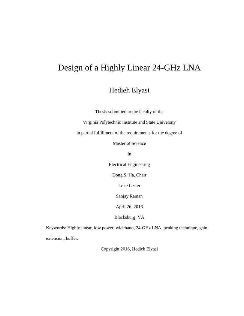
There are many different applications (Fig. 1-1) for around 24-GHz LNA design in
both industry and academia [8]-[13].The Federal Communications Commission (FCC)
has devoted 24-GHz frequency band for unlicensed industrial, scientific, and medical
(ISM) applications to avoid interference in overcrowded areas and wideband signal
transmission [4], [14], [15]. Short range and high data rate wireless communication and
automotive radar are some examples of these applications.
Automotive radar sensors has been widely used during these years [16]. Mounting
several short range sensors around the vehicle leads to achieving short range (0 - 40 m)
driver and security assistance such as collision avoidance, precise airbag activation,
parking and lane change assistance, and many other applications [17]. Local positioning
is another application in museums for guiding purposes.
24-GHz Applications
Human Detection Automotive RadarNoncontact Vital Sign
Detection
Earthquake
Victims
Avalanches
VictimsCollision
Avoidance
Humans Behind
Barriers
Cardiopulmonary
Detection
Apnea
Detection
Respiration
rateBlind Spot Detection
Lane
Change Aid
Airbag Activation
Parking Assistance
Fig. 1-1 24-GHz applications

2
The other use of the Doppler radar is noncontact vital-sign sensing and mechanical
vibration detection [18]–[22]. It has been used for respiration rate and apnea detection
in 1975. In the early 1980s, it has been used for finding victims in earthquakes or
avalanches [23] and finding humans behind barriers [24]. Cardiopulmonary detection is
another example of its use in 2004 [25].
1.2 Review of 24-GHz LNAs
LNA is a very critical building block in receiver design, and depending on the
application, both its NF and linearity performance need to be improved while keeping
the power consumption low. Many techniques have been introduced for noise figure
reduction like noise cancellation presented in [26]-[28]. For linearization also, many
techniques have also been suggested for 𝑔𝑚" cancellation [ 29 ]-[ 33 ]. But in high
frequency LNA design, RF IC designers prefer minimizing extra parasitic and coupling
effects using simple circuit architectures. Since those effects can provides positive
feedback or make the analysis very complicated. However, there are cases that the
coupling effect between inductors is desirable in order to decrease the inductor size or
achieve better performance.
Multi stage transistors are widely used for achieving higher gain or attaining either
minimum NF or maximum linearity in each stage. In other words, the first stage can be
designed for minimum noise generation and higher gain, while the latter stage can focus
on maximum linearity performance. The other application of multi stage LNA is making
wide band LNA by resonating out the load inductors at different frequencies, at the
expense of a slight gain penalty [35]. Some examples of most recent works has been
reviewed here.
As an example, [34] uses five stage LNA to achieve the gain of 15 dB at 90-GHz
frequency. Since the first stage has highest effect on the total NF, according to the Friis
equation, the first two stages are designed for minimum noise figure. In fact, the high
pass L- and п-matching networks are opted for this purpose.
In [35], cascode topology with shunt peaking technique is utilized for better isolation
and higher gain (Fig. 1-3). The peaking inductor resonates out the existing parasitic

3
capacitance and provides image rejection. The equivalent impedance of the peaking
network, surrounded in dashed rectangular is as below;
𝑍𝑖𝑛 =1 + 𝑠2𝐿𝑝𝐶𝑠
𝑠[𝐶𝑝 + 𝐶𝑠 + 𝑠2𝐶𝑠𝐶𝑝𝐿𝑝] (1-1)
Accordingly, there is a zero at (𝐿𝑝𝐶𝑠)−1/2
and a pole at [𝐿𝑝𝐶𝑠𝐶𝑝/(𝐶𝑠 + 𝐶𝑝)]−1/2
which results in RF signal attraction and image signal rejection.
Fig. 1-4 is a two stage LNA that has been used in [36] to have NF optimization in
the first stage and gain boosting in the second stage. Accordingly, the former stage is a
common source amplifier while the latter is cascode for having higher gain and slightly
higher noise.
out
in
Fig. 1-2 Five-stage LNA for W-band [34]
out
inL1
LD
Lp
Cs
Cp Lp
Vb
L2
C2
M1
M2
Cb
Rb
C1
shunt peaking
Fig. 1-3 Shunt peaking technique [35]

4
out
in
Fig. 1-4 K-band LNA [36]
1.3 Research Objective
The objective of the proposed work is to design a highly linear LNA with high gain
and low NF while the power consumption is low. To reduce the NF effect of the
following blocks on overall receiver NF performance, the gain of the LNA needs to be
high. However, linearity has a trade off with gain, and achieving both is very
challenging especially in terms of keeping the power consumption low.
In high frequency LNA design, stability is another concern because of feedthrough
from parasitic capacitances which needs to be taken into account in wide range of
frequency.
1.4 Contribution and Proposed Research
The main contribution of this work can be mentioned as below;
Design, analysis, and implementation of a novel wideband LNA in 24-GHz
frequency range using 8XP 0.13-µm SiGe BiCMOS technology.
Proposing a new linearization technique, called peaking technique. It
enhances 1-dB compression point and expands gain flatness region in overall
system performance. The proposed design has control voltage which makes
it appropriate for different receiver designs.
Suggesting a new buffer to have additive gain from two directions, enhancing
the gain and linearity without consuming higher power.

5
Assigning variable control voltage, different linearity and gain can be
achieved, regarding desired application.
1.5 Thesis Organization
The remainder of this thesis work has been organized as follows. The prerequisites
of this research work, different topologies in LNA design at high frequency, its design
parameters, and optimal sizing and biasing are discussed in chapters 2 and 3. Chapter 4
proposes the new linearization and gain expansion technique, and the effectiveness of
the suggested technique has been illustrated in chapter 5. Finally, in chapter 6
conclusion of this work is summarized.

6
Chapter 2. Preliminaries
2.1 Introduction
This chapter devoted to prerequisite of LNA design. At first, silicon technology
versus SiGe and bipolar technology versus CMOS are compared to show the reason of
choosing SiGe BiCMOS technology for this LNA design. Then important parameters
of bipolar transistor such as its noise and linearity have been studied.
2.2 Si versus SiGe
SiGe has higher 𝛽 in comparison with silicon. Therefore, for the same amount of
collector current, the base current is lower in SiGe technology. SiGe technology also
offers higher 𝑓𝑇 compared to Si technology for having smaller base and emitter transit
time. Hence, for a same amount of gain, SiGe needs smaller collector current than Si
technology.
2.3 CMOS versus Bipolar
CMOS technology has small size and high gain while bipolar devices has large size,
high power, and good frequency response. Bipolar transistor is a choice for high current
applications while CMOS transistors are better opt for high voltage uses.
The collector current of bipolar transistor can be achieved using below equation;
𝑖𝐶 = 𝐼𝑠𝑒𝑣𝐵𝐸
𝑛𝑉𝑇⁄
(2-1)
where
𝐼𝑠 =𝑞𝐴𝐷𝑛 𝑛𝑖
2
𝑄𝐵 (2-2)
and 𝐷𝑛 is the diffusion constant of the electrons, 𝑛𝑖 is the intrinsic carrier concentration,
and 𝑄𝐵 is the total number of impurity atoms per unit area. The current of CMOS
transistor in saturation is;
𝑖𝐷 =1
2µ𝑛𝐶𝑜𝑥
𝑤
𝑙(𝑣𝐺𝑆 − 𝑉𝑡ℎ)
2 (2-3)

7
EB
rb1 rb2
C
Substrate
n
p
n+
Fig. 2-1 series base resistance
Collector Current
Bas
e R
esis
tanc
e
Fig. 2-2 Base resistance variation versus collector current
Bipolar technology is faster than CMOS because it deals with bulk mobility rather
than surface mobility in MOSFET. The speed of MOSFET can be increased by
decreasing 𝑣𝐺𝑆 − 𝑉𝑡ℎ, although it has side effects like transconductance reduction, gain
degradation, and slow increase of carrier velocity because of velocity saturation [44].
The SiGe bipolar technology has a robust model at high frequencies which makes it
a better selection compared to CMOS technology at high frequencies [37]-[40]; in spite
of its higher cost and integration issue.
2.4 HBT important parameters
In bipolar circuit design, some parameters should be considered like fT and fmax of the
transistor, its noise sources, and nonlinearity sources, which is discussed in this section.

8
2.4.1 Series Base Resistance
There is a noticeable series ohmic base resistance in bipolar transistors. It is sited
between the contact and the active base region as the base contact is physically removed
from the active base region [44].
This series base resistance can be separated in two parts;
I. Between base contact and the edge of the emitter diffusion (𝑟𝑏1).
II. Between the edge of the emitter and the site within the base region (𝑟𝑏2).
The first base resistance part is a function of sheet resistance while the second one is
complicated and has different values for different bias conditions. Therefore, at a given
SiGe technology, 𝑟𝑏1 is fixed. At moderate current level, most of the injection happens
near the emitter diffusion edge while at higher current levels, all of it takes place at the
emitter diffusion edge and as a result 𝑟𝑏1 ≅ 𝑟𝑏2 [41].
2.4.2 fT and fmax
There is always a hot debate regarding using whether fT or fmax in circuit design.
Transition frequency or 𝑓𝑇 is the extrapolated frequency in which the small signal
current gain with a shorted output reaches to unity, depicted in Fig. 2-3.
Therefore, both are narrow band small signal parameters depending on biasing
condition. Consequently, they are not good opt for large signal performance prediction
and because of not providing phase information, not suitable for time domain transient
response as well [44].
Transit or cut-off frequency can be defined according to its definition which would
be;
|𝑖𝑜𝑢𝑡𝑖𝑖𝑛
| = |𝑔𝑚𝑣𝑖𝑛𝑣𝑖𝑛 𝑍𝑖𝑛⁄
| = |𝑔𝑚𝑍𝑖𝑛| = |𝑔𝑚 (1
𝑗𝜔𝑇𝐶𝑖𝑛)| = 1 (2-4)
𝑓𝑇 ≅𝑔𝑚2𝜋𝐶𝑖𝑛
(2-5)
Maximum frequency is the extrapolated frequency in which the small signal power
gain with a conjugate matching condition reaches to unity and can be achieved using
below equation;

9
𝑓𝑀𝑎𝑥 = √𝑓𝑇
8𝜋𝐶𝑗𝑐𝑟𝑏 (2-6)
Higher 𝑓𝑀𝑎𝑥 demands lower base resistance while fT is independent of base
resistance.
To put it in a nutshell, depending on the application different requirement is needed
for fT and fmax [42]:
In tuned IC designs fmax determines the gain and maximum operating
frequency. However, a low fT/fmax ratio may limit the tuning range.
In lumped analog IC design high fT/fmax ratio, typically 1.5:1, is needed.
In distributed amplifiers, fmax is more important.
Fig. 2-4 shows the transit frequency of a bipolar transistor as a function of current
density. Simulation is done for 1-µm emitter length 8XP SiGe transistor applying 1.3 V
collector emitter voltage in Cadence cad tool.
SiGe HBT transistors have lower base resistance in comparison with silicon homo-
junction transistors, because the base of the former has heavier base doping compared
to the latter one [43].
iin
Q1
vin
+
-Cin
iout
ac
GND
Fig. 2-3 Conceptual transit frequency (fT) calculation set up

10
100
150
200
250
300
0 5 10 15 20
f T (
GH
z)
JC (mA/µA2)
Fig. 2-4 fT versus Jc
2.5 Bipolar Noise Sources
Bipolar transistors have relatively low noise characteristics. Since the lower limit of
the dynamic range is set through the noise floor, it has a great importance in wireless
circuit design.
2.5.1 Shot Noise
Shot noise refers to the carrier’s fluctuation across a potential barrier like p-n
junction. This fluctuation leads to random currents and its mean square current value
can be achieved using below equation;
𝑖𝑛2 = 2𝑞𝐼𝐷𝐶∆𝑓 (2-7)
In bipolar transistors, assuming negligible delay in the collector-base junction, we
have;
𝑖𝑏2 = 2𝑞𝐼𝐵∆𝑓 (2-8)
𝑖𝑐2 = 2𝑞𝐼𝐶∆𝑓 (2-9)
For the same collector current, SiGe has a lower base current compared to Si bipolar
transistor as a result of higher 𝛽 [44].
2.5.2 Thermal Noise
Connecting a voltmeter across a resistor, a voltage appears, which is independent of
voltage source and will appear even without voltage source. This random number is

11
thermal noise, and has an average of zero. Hence, its mean square voltage can be
considered as its figure of merit, attained using below equation;
𝑣𝑛2 = (𝑣 − )2 = lim
𝑇→∞∫ (𝑣 − )2𝑑𝑡𝑇
0
(2-10)
The Power Spectral Density (PSD) of the voltage noise, 𝑆𝑣(𝑓), can be defined as;
𝑆𝑣 = 4𝐾𝑇𝑅 (2-11)
And
𝑣𝑛2 = 4𝐾𝑇𝑅∆𝑓. (2-12)
Using Thevenin’s equation the mean square current value would be;
𝑖𝑛2 = 4𝐾𝑇
1
𝑅∆𝑓. (2-13)
Assuming no frequency dependency, this noise is known as white noise.
2.5.3 Bipolar Noise Model
The main noise sources of an LNA are thermal noise because of base resistance and
shot noise due to base and collector DC current, depicted in Fig. 2-5.
According to the source termination admittance (𝑌𝑠 = 𝐺𝑠 + 𝑗𝐵𝑠 ), optimal noise
source admittance, noise resistance, and minimum noise figure value, the noise figure
of the circuit can be determined [45].
NF = 𝑁𝐹𝑚𝑖𝑛 +R𝑛𝐺𝑠|𝑌𝑠 − 𝑌𝑠,𝑜𝑝𝑡|
2. (2-14)
in,c2
Vn,rb2
in,b2
Fig. 2-5 Bipolar noise sources model

12
Vn,a2
in,a2
V1
V2
I2
I1
Fig. 2-6 Equivalent two port noise sources
Obviously, minimum noise figure can be achieved when 𝑌𝑠 = 𝑌𝑠,𝑜𝑝𝑡. When 𝑌𝑠 and
𝑌𝑠,𝑜𝑝𝑡 are not equal, 𝑅𝑛 determines how fast NF increases when 𝑌𝑠 deviates from 𝑌𝑠,𝑜𝑝𝑡.
In many cases, admittances different from 𝑌𝑠,𝑜𝑝𝑡 are choosing for achieving higher gain,
since optimum admittance for noise matching is different from gain matching. Finding
the noise sources of 𝑖𝑛𝑎, 𝑣𝑛𝑎, and their correlations, minimum noise figure of a linear
two port system can be achieved using below equation and is explained in details earlier
[45].
𝑁𝐹𝑚𝑖𝑛 = 1 + 2R𝑛(𝐺𝑠,𝑜𝑝𝑡 +𝑅𝑒S𝑖𝑛𝑣𝑛∗
S𝑣𝑛). (2-15)
where 𝐺𝑠,𝑜𝑝𝑡 = √𝑆𝑖𝑛
𝑆𝑣𝑛− (
𝐼𝑚(𝑆𝑖𝑛𝑣𝑛∗ )
S𝑣𝑛)2
and 𝐵𝑠,𝑜𝑝𝑡 = −𝐼𝑚(𝑆𝑖𝑛𝑣𝑛
∗ )
𝑆𝑣𝑛. The parameters of 𝑆𝑖𝑛𝑣𝑛∗ ,
𝑆𝑣𝑛, and 𝑅𝑛 can be obtained using below equations;
𝑆𝑖𝑛𝑣𝑛∗ =1
∆𝑓
𝑖𝑐𝑌21
(𝑌11𝑌21
𝑖𝑐)∗
= 2𝑞𝐼𝑐𝑌11∗
|𝑌21|2. (2-16)
𝑆𝑣𝑛 =
2q𝐼𝑐|𝑌21|
2
(2-17)
𝑅n =
𝑆𝑣𝑛4𝑘𝑇
(2-18)
In bipolar transistor, lower current is preferred for lower power consumption,
minimal fT reduction, and less noise contribution. Largest emitter length of transistor is
desired for having a smaller base resistance; although, it contributes larger power

13
consumption and parasitic junction capacitance. When collector shot noise is the
dominant noise source, increasing the collector current improves the noise performance.
Because in spite of the fact that collector shot noise power increases with current surge,
the signal power gain also rises with current square factor.
2.6 Linearity
In an actual system, the output signal is not linearly related to the input signal. Any
nonlinear memoryless system can be approximated writing a Taylor series;
𝑣𝑜𝑢𝑡 = 𝑘0 + 𝑘1𝑣𝑖𝑛 + 𝑘2𝑣𝑖𝑛2 + 𝑘3𝑣𝑖𝑛
3 +⋯ (2-19)
In most of the cases, the first three terms provide enough accuracy for characterizing
the circuit. However, for systems with memory, Volterra series expansion is
recommended [46].
2.6.1 Linearity in bipolar
Writing a KVL from the base input to the emitter and the ground node;
𝑉 + 𝑣𝑖𝑛 = 𝑉𝐵𝐸 + 𝑣𝑏𝑒 + 𝑅𝐸(𝐼𝐶 + 𝑖𝑐) (2-20)
Therefore;
𝑣𝑖𝑛 = 𝑣𝑏𝑒 + 𝑅𝐸𝑖𝑐 (2-21)
As mentioned earlier, the relation between collectors current and base emitter voltage
can be written as below;
𝐼𝐶 + 𝑖𝑐 = 𝐼𝑠𝑒𝑉𝐵𝐸+𝑣𝑏𝑒
𝑉𝑇 = 𝐼𝑠𝑒𝑉𝐵𝐸𝑉𝑇 × 𝑒
𝑣𝑏𝑒𝑉𝑇 = 𝐼𝐶𝑒
𝑣𝑏𝑒𝑉𝑇 (2-22)
As a result;
𝑣𝑏𝑒 = 𝑉𝑇 ln(1 +𝑖𝑐𝐼𝐶) (2-23)
According to the Taylor series;
ln(1 + 𝑥) = 𝑥 −𝑥2
2+𝑥3
3−⋯ (2-24)
Consequently,

14
RC
vout
V+vin
RE
Fig. 2-7 resistive degeneration bipolar transistor
𝑣𝑖𝑛 = 𝑅𝐸𝑖𝑐 + 𝑉𝑇 [𝑖𝑐𝐼𝐶−1
2(𝑖𝑐𝐼𝐶)2
+1
3(𝑖𝑐𝐼𝐶)3
−⋯] (2-25)
𝑣𝑖𝑛 = (𝑅𝐸 + 𝑟𝑒)𝑖𝑐 −1
2𝑟𝑒𝑖𝑐2
𝐼𝐶+1
3𝑟𝑒𝑖𝑐3
𝐼𝐶2 −⋯ (2-26)
Dividing both sides by 𝑅𝐸 + 𝑟𝑒;
𝑣𝑖𝑛/(𝑅𝐸 + 𝑟𝑒) = 𝑖𝑐 −1
2
𝑟𝑒𝑅𝐸 + 𝑟𝑒
𝑖𝑐2
𝐼𝐶+1
3
𝑟𝑒𝑅𝐸 + 𝑟𝑒
𝑖𝑐3
𝐼𝐶2 −⋯ (2-27)
There is a rule in Taylor series which says; when
𝑦 = 𝑎1 + 𝑎2𝑥2 + 𝑎3𝑥
3 +⋯ (2-28)
x can be written as
𝑥 = 𝑏1 + 𝑏2𝑦2 + 𝑏3𝑦
3 +⋯ (2-29)
if 𝑏1 =1
𝑎1, 𝑏2 =
−𝑎2
𝑎13 , 𝑏3 =
2𝑎22−𝑎1𝑎3
𝑎13 , etc.
Therefore, 𝑖𝑐 can be written as a function of 𝑣𝑖𝑛;
𝑖𝑐 =𝑣𝑖𝑛
𝑅𝐸 + 𝑟𝑒+
1
2𝐼𝐶(
𝑟𝑒𝑅𝐸 + 𝑟𝑒
) (𝑣𝑖𝑛
𝑅𝐸 + 𝑟𝑒)2
+ (1
2𝐼𝐶2 (
𝑟𝑒𝑅𝐸 + 𝑟𝑒
)2 −1
3𝐼𝐶2 (
𝑟𝑒𝑅𝐸 + 𝑟𝑒
)) (𝑣𝑖𝑛
𝑅𝐸 + 𝑟𝑒)3
(2-30)

15
2.7 Summary
In this chapter, a comparison of bipolar and CMOS transistor and the reason bipolar
transistor has been chosen in this research has been studied. Important design
parameters of a bipolar transistor, including transit frequency, maximum frequency,
noise modeling, and linearity analysis of bipolar transistors have been discussed.

16
Chapter 3. LNA Prerequisite
3.1 Introduction
LNA is the first building block in a receiver and its performance is very critical for
overall receiver performance. The NF of an LNA has the most contribution in the overall
receiver’s NF value and its gain determines how much the noise of the next stages can
relax. Therefore, having a high gain and a low NF for the LNA is desirable. However,
the high gain of LNA enforces the next stages to be more linear since they suffer from
larger signal levels at their input stage and can get saturated easily. As a result, there has
always been a tradeoff between gain, NF and linearity.
3.2 LNA Design parameters
The main design parameters of an LNA has been explained in this section.
3.2.1 Gain
The gain of LNA needs to be large enough to attenuate the noise from the next stages,
and its following blocks design be slightly relaxed in terms of noise. However, gain has
trade off with linearity and usually power consumption. Unlike NF, the linearity of the
afterward stages of the LNA would be more challenging when the gain of LNA is high.
Because they have to suffer larger signal levels. The gain of different LNA topologies
has been studied in section 3.3.
3.2.2 NF
NF of LNA can be achieved simply from noise figure equation;
NF =𝑉𝑛,𝑜𝑢𝑡2
4𝐾𝑇𝑅𝑠𝐴𝑣2 (3-1)
where 𝐴𝑣 is the gain of the LNA and √𝑉𝑛,𝑜𝑢𝑡2 is the noise mean square voltage at the
output of the LNA.
Minimum noise figure of two port system needs to be calculated for LNA design.

17
in
vn
Ys
Ai
ins
iin iout
Noiseless Cicuit
Fig. 3-1 equivalent noise sources of two ports circuit
Considering the system shown in Fig. 3-1, the noise of the circuit with gain of Ai can
be modeled, with two input voltage and current noise sources namely vn and in. Each of
the noise sources can be defined as sum of its correlated and uncorrelated part, as below;
𝑖𝑛 = 𝑖𝑐+𝑖𝑢 (3-2)
𝑣𝑛 = 𝑣𝑐+𝑣𝑢 (3-3)
Assuming correlated current and voltage are related by Yc factor (𝑖𝑐 = 𝑌𝑐𝑣𝑐), NF
equation can be found;
𝑁𝐹 =𝑖𝑛𝑠2 + |𝑖𝑛 + 𝑣𝑛𝑌𝑠|
2
𝑖𝑛𝑠2
= 1 +𝑖𝑢2 + |𝑌𝑐 + 𝑌𝑠|
2𝑣𝑐2 + 𝑣𝑢
2|𝑌𝑠|2
𝑖𝑛𝑠2
(3-4)
Accordingly following parameters can be defined;
𝑅𝑐 =𝑣𝑐2
4𝐾𝑇∆𝑓 (3-5)
𝑅𝑢 =𝑣𝑢2
4𝐾𝑇∆𝑓 (3-6)
𝐺𝑢 =𝑖𝑢2
4𝐾𝑇∆𝑓 (3-7)
𝐺𝑠 =
𝑖𝑛𝑠2
4𝐾𝑇∆𝑓
(3-8)
Each Yc and Ys can also be defined as sum of real and imaginary part;
𝑌𝑐 = 𝐺𝑐+j𝐵𝑐 (3-9)
18
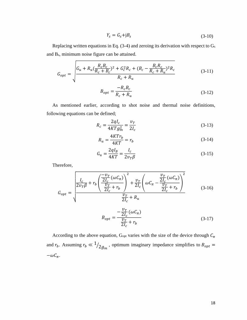
𝑌𝑠 = 𝐺𝑠+j𝐵𝑠 (3-10)
Replacing written equations in Eq. (3-4) and zeroing its derivation with respect to Gs
and Bs, minimum noise figure can be attained.
𝐺𝑜𝑝𝑡 =
√𝐺𝑢 + 𝑅𝑢(
𝑅𝑐𝐵𝑐𝑅𝑐 + 𝐵𝑐
)2 + 𝐺𝑐2𝑅𝑐 + (𝐵𝑐 −
𝐵𝑐𝑅𝑐𝑅𝑐 + 𝑅𝑢
)2𝑅𝑐
𝑅𝑐 + 𝑅𝑢
(3-11)
𝐵𝑜𝑝𝑡 =−𝑅𝑐𝐵𝑐𝑅𝑐 + 𝑅𝑢
(3-12)
As mentioned earlier, according to shot noise and thermal noise definitions,
following equations can be defined;
𝑅𝑐 =2𝑞𝐼𝑐
4𝐾𝑇𝑔𝑚2=𝑣𝑇2𝐼𝑐
(3-13)
𝑅𝑢 =4𝐾𝑇𝑟𝑏4𝐾𝑇
= 𝑟𝑏 (3-14)
𝐺𝑢 =2𝑞𝐼𝐵4𝐾𝑇
=𝐼𝑐
2𝑣𝑇𝛽 (3-15)
Therefore,
𝐺𝑜𝑝𝑡 =
√
𝐼𝑐2𝑣𝑇𝛽
+ 𝑟𝑏 (
−𝑣𝑇2𝐼𝑐
(𝜔𝐶𝜋)
𝑣𝑇2𝐼𝑐
+ 𝑟𝑏)
2
+𝑣𝑇2𝐼𝑐
(𝜔𝐶𝜋 −
𝑣𝑇2𝐼𝑐
(𝜔𝐶𝜋)
𝑣𝑇2𝐼𝑐
+ 𝑟𝑏)
2
𝑣𝑇2𝐼𝑐
+ 𝑅𝑢
(3-16)
𝐵𝑜𝑝𝑡 =−𝑣𝑇2𝐼𝑐
(𝜔𝐶𝜋)
𝑣𝑇2𝐼𝑐
+ 𝑟𝑏 (3-17)
According to the above equation, Gopt varies with the size of the device through 𝐶𝜋
and 𝑟𝑏. Assuming 𝑟𝑏 ≪12𝑔𝑚⁄ , optimum imaginary impedance simplifies to 𝐵𝑜𝑝𝑡 =
−𝜔𝐶𝜋.

19
20log(vin )
20lo
g(v o
ut)
vin,1dB
Fig. 3-2 Finding Pin,1dB
3.2.3 P1dB
One way of measuring the linearity is finding the 1-dB compression point. The
input/output P1dB is the input/output power level in which thgete output power of the
system would be 1 dB less than the expected linear output power. It could be found
using below equation according to Fig. 3-2;
20 log(𝑣𝑜𝑢𝑡𝑘1𝑣𝑖𝑛
) = −1. (3-18)
Applying single frequency at the input, the cube of 𝑣𝑖𝑛 term (𝑣𝑖𝑛3 ) would create a
suppression in gain according to the sin(𝜃)3 =
3
4sin(𝜃) −
1
4sin(3𝜃) because it would
create a term in desired frequency. Therefore,
𝑘1𝑣𝑖𝑛 +
34𝑘3𝑣𝑖𝑛
3
𝑘1𝑣𝑖𝑛= 0.89125 (3-19)
𝑣1𝑑𝐵 = 0.22√𝑘1𝑘3
(3-20)
However, considering more harmonics, this voltage would be lower. Accordingly,
the 1-dB compression point of the resistive degenerated bipolar transistor shown in
Fig. 2-7 can be found using Eq. (2-30).

20
𝑣1𝑑𝐵 = 0.22√
1
𝑅𝐸 + 𝑟𝑒×6𝐼𝐶
2 × (𝑅𝐸 + 𝑟𝑒)5
1 − 2𝑅𝐸𝑟𝑒
(3-21)
Simplifying Eq. (3-21), following equation can be achieved;
𝑣1𝑑𝐵 = 0.22√6𝑟𝑒𝐼𝐶
2 × (𝑅𝐸 + 𝑟𝑒)4
|2𝑅𝐸 − 𝑟𝑒| (3-22)
Therefore, for larger 𝐼𝐶 and 𝐼𝐵, linearity is better. In above equation, if 𝑅𝐸 set in a
way that 𝑅𝐸 =𝑟𝑒
2, the third order term will be cancelled. For lower resistive degeneration
value, the third order nonlinear term would be positive which means the gain expansion
would happen. While for larger values, this term would be negative and gain
compression is expected.
3.3 LNA topologies
There are different topologies in bipolar LNA design like common emitter, common
base, cascode structure, and common collector.
3.3.1 Common Emitter Amplifier
Common emitter has been widely used because of its high gain and simplicity
(Fig. 3-3). However, it suffers from the dependence of the input impedance of the
transistor on the load impedance through the base collector capacitance. In fact,
according to the high gain of the transistor, the miller capacitance of the base collector
would be effective;
𝐶𝑀1 = 𝐶µ(1 − 𝐴𝑣) (3-23)
𝐴𝑣 = −𝐺𝑚𝑍𝐿 (3-24)
The other issue with the common emitter structure is the stability issue in high
frequency designs. Fig. 3-4 shows a common emitter amplifier and its small signal
model considering parasitic capacitances. Accordingly, the input impedance of 𝑍𝑖𝑛
would be;

21
𝑌𝑖𝑛 =1𝑍𝑖𝑛⁄ =
1
𝑟𝜋+ (𝐶𝜋 + 𝐶µ)𝑠 −
𝐶µ𝑠(𝐶µ𝑠 − 𝑔𝑚)
1 𝑍𝐿⁄ + 𝐶µ𝑠 (3-25)
Therefore, the negative impedance can appear in the above equation which causes
instability as a result of positive feedback. Assuming the load is inductive, 1 𝑍𝐿⁄ +
𝐶µ𝑠 = 1 𝐿𝑥𝑠⁄ , and ignoring 𝑟𝑏 the input admittance would be;
𝑌𝑖𝑛 =1
𝑟𝜋+ (𝐶𝜋 + 𝐶µ − 𝐶µ
2𝜔2𝐿𝑋)𝑠 − 𝐶µ2𝐿𝑥𝑔𝑚
(3-26)
Therefore, having 1
𝑟𝜋< 𝐶µ
2𝐿𝑥𝑔𝑚, the input admittance would have negative real part
which can cause instability.
Cµ
ZL
CM1
CM2
ZL
(a) (b)
Fig. 3-3 common emitter amplifier including (a) parasitic collector-base capacitance
(b) miller capacitance
Zin
ZL
vout
vinRs
ZLgmVbe
Cµ
Cπ rπ
Rs+rb voutvin
(a) (b)
Fig. 3-4 (a) input impedance of common emitter, (b) small signal model of (a)
The gain of common emitter amplifier can be attained using below equation;
𝑣𝑜𝑢𝑡𝑣𝑖𝑛
=𝐴𝑣0
1 + 𝑗𝑓𝑓𝑝1
(3-27)
where for the input matched case

22
𝐴𝑣0 =𝑣𝑜𝑢𝑡𝑣𝑖𝑛
=1
2×
𝑟𝜋𝑟𝜋 + 𝑟𝑏
𝑔𝑚𝑍𝐿 (3-28)
𝑓𝑝1 =1
2𝜋(𝑟𝜋‖ (𝑟𝑏 + 𝑅𝑠))(𝐶𝜋 + 𝐶𝜇𝑔𝑚𝑍𝐿) (3-29)
3.3.2 Common Base Amplifier
Common base amplifier attracts attention because of its low input impedance over a
wide range of frequencies. When area and power consumption are matter, common base
amplifier is a good choice since it does not need inductor for matching purpose. Its small
signal model has been shown in Fig. 3-5 which has below current gain;
𝑖𝑜𝑢𝑡𝑖𝑖𝑛
≈1
1 + 𝑗𝜔𝐶𝜋𝑟𝑒≈
1
1 + 𝑗𝜔𝜔𝑇
(3-30)
For the input matched case, the voltage gain would be;
𝑣𝑜𝑢𝑡𝑣𝑖𝑛
≈1
1 + 𝑗𝜔𝜔𝑇
×𝑍𝐿2𝑅𝑠
(3-31)
Common base amplifier is wide band and has superior linearity, stability, and
robustness to PVT variation [47] but unfortunately, it has higher NF compared to the
common emitter amplifier.
3.3.3 Cascode Amplifier
To take the advantage of both common emitter and common base amplifier, cascode
structure has been introduce which has higher gain, better isolation at the expense of
slightly higher noise. The other disadvantage of cascode structure is its additional pole
which causes problem when the load is large. This fact leads to a rapid high frequency
gain roll off and an excess phase lag, which can be problematic when feedback is used.
Additional bias circuit for the second transistor and reduced signal swing at a given
supply voltage are the ultimate challenges in cascode design [48].

23
ZL
vout
vin
Rs
ZLgmVbe
Cµ
Cπ rπ
rb vout
vin
iin iout
(a) (b)
Fig. 3-5 common base amplifier (a) schematic (b) small signal model.
ZL
vin
Bias
vout
Rs
Q2,cascode
Q1,driver
Fig. 3-6 Cascode amplifier
As depicted in Fig. 3-7 (a), the current passing through the 𝑄1 is almost the same as
the current passing through the 𝑄2 , because of mentioned near one current gain.
Therefore, the gain is almost;
𝐴𝑣0 = −𝑔𝑚𝑍𝐿 (3-32)
However, the miller effect has been reduced because of the reduced impedance of
the 𝑍𝐿,𝑐𝑎𝑠𝑐𝑜𝑑𝑒 depicted in Fig. 3-7 (b).
𝑍𝐿,𝑐𝑎𝑠𝑐𝑜𝑑𝑒 ≈1𝑔𝑚⁄ (3-33)
Therefore, the pole will change to;

24
Cµ
ZL
ZL,cascode
Q2,
Q1
CM2
ZL
Q2,
Q1
CM1
(a) (b)
Fig. 3-7 Miller effect in cascode amplifier
𝑓𝑝1 =1
2𝜋(𝑟𝜋1‖(𝑟𝑏1 + 𝑅𝑠))(𝐶𝜋 + 2𝐶µ) (3-34)
3.3.4 Common Collector (Emitter Follower) Amplifier
There is another architecture, common collector or emitter follower, which mainly
uses as buffer for isolation or matching purpose. This architecture is robust against load
and PVT (Process Voltage Temperature) variations. The importance of this architecture
is having a high input impedance while the output impedance is low. This architecture
and its small signal model has been shown in Fig. 3-8. As the collector is grounded,
miller effect is not an issue in this architecture. The voltage gain of this amplifier is
given by;
𝐴𝑣(𝑠) = 𝐴𝑣0 (1 − 𝑠 𝑓𝑧1⁄
1 − 𝑠 𝑓𝑝1⁄) (3-35)
where
𝐴𝑣0 =𝑔𝑚𝑅𝐸 +
𝑅𝐸𝑟𝜋
1 + 𝑔𝑚𝑅𝐸 +𝑅𝑠 + 𝑟𝑏 + 𝑅𝐸
𝑟𝜋
≈𝑔𝑚𝑅𝐸
1 + 𝑔𝑚𝑅𝐸≈ 1
(3-36
)
𝑓𝑧1 ≈𝑔𝑚𝐶𝜋
(3-37
)

25
vout
vin
RE
Rs
gmVbe
Cµ
Cπ rπ
Rs+rb
vout
vin
RE
(a) (b)
Fig. 3-8 Emitter follower (a) schematic, (b) small signal model
𝑓𝑝1 ≈
1
𝐶𝜋(𝑟𝜋 ‖𝑅𝑠 + 𝑟𝑏 + 𝑅𝐸
𝑔𝑚𝑅𝐸)
(3-38)
3.4 Matching Network
Since LNA is the first block of the receiver and may be connected to the off chip
cpomponents, its matching is very important. There are various matching networks with
varying bandwidth and complexity. In wireless systems, usually there is a trade off
between noise and input matching network [49], [50], especially, in cases were the noise
matching has been provided through the passive network for a given transistor size. But
the passive networks are themselves lossy and origin of NF degradation. Therefore, it
is better to first change the size of the transitor to get the minmium noise perfromance
and accordinly design a very simple matching network.
The most popular matching network considering simplicity and having minimum NF
has been discussed in [51] and depicted in Fig. 3-9. It provides a perfect matching
without adding any noise to the system.
Considering the capacitance at the base as a decoupling capacitance, the input
impedance, writing the KVL and KCL equations regarding to the equivalent small
signal model would be (Fig. 3-10).
𝑍𝑖𝑛 = 𝐿𝐸𝑠 + 𝑟𝑏 +
1
𝐶𝜋𝑠+ 𝐿𝐸(1 + 𝛽) = (𝐿𝐵 + 𝐿𝐸)𝑠 +
1
𝐶𝑏𝑒𝑠+ 𝑟𝑏 +
𝑔𝑚𝐿𝐸𝐶𝑏𝑒
= 50 𝛺
(3-39)

26
Zin
Q1
LB
LE
Fig. 3-9 Matching of LNA using two inductors
Zin
LB rb
Cп rп
LE
gm
ioutCjc
Zin
LB rb
Cп
LE(1+β )
(a) (b)
Fig. 3-10 Input impedance of driver transistor (a) pi-model (b) simplified equivalent
Knowing 𝑟𝑏 and 𝐶𝑏𝑒 because of device size, 𝐿𝐸 can be determined.
𝑔𝑚𝐿𝐸𝐶𝜋
+ 𝑟𝑏 = 𝑅𝑠 (3-40)
As a result
𝐿𝐸 =(𝑅𝑠 − 𝑟𝑏)𝐶𝜋
𝑔𝑚=𝑅𝑠 − 𝑟𝑏𝜔𝑇
. (3-41)
The imaginary part also needs to be equal to zero which means,
𝐿𝐵 =1
𝐶𝜋𝜔2−𝑅𝑠𝐶𝜋𝑔𝑚
(3-42)
It should be noted that 𝐿𝐵 can be chosen in a way to have a good matching in spite
of not having thorough parasitic capacitance cancellationn. The achievement of this
inductance opt can be attaining lower NF. For perfect matching purpose the real part of
𝑍𝑖𝑛 needs to be equal to the source resistance, 𝑅𝑠.
This matching technique is simple and relatively broad band. It also can provide
simultaneous noise and power matching. However, this network is not applicable for

27
cases were minimum noise performance requires very high current or desired current
cannot meet the minimum noise condition. The other concern can be requirng higher
degeneration inductor for linearity improvement purpose.
3.5 Optimal Sizing and Biasing of LNA
In LNA design, it is good to know how the minimum NF would change regarding
transistors’ size scaling.
3.5.1 Emitter Width Scaling
Assuming base resistance, 𝑟𝑏, as the dominant noise source, having two transistors
with different emitter width affect the minimum noise figure value.
Considering 𝑊𝐸𝑟 as the reference and 𝑊𝐸𝑠 as the scaled one where 𝑊𝐸𝑠 = 𝑀 ×𝑊𝐸𝑟
and 0 < 𝑀 < 1, and assuming same base emitter voltage of 𝑣𝐵𝐸 for both cases, the
𝑁𝐹𝑚𝑖𝑛 can be compared for these two cases.
Having same 𝑣𝐵𝐸, the current density (𝐽𝑐) would be same. As mentioned earlier, 𝑓𝑇
is a function of 𝐽𝑐 , which means both cases would have an equal 𝑓𝑇 . Therefore, the
𝑁𝐹𝑚𝑖𝑛 value changes as below [44];
𝑁𝐹𝑚𝑖𝑛,𝑠 = 1 +1
𝛽+ √2𝑔𝑚,𝑠𝑟𝑏,𝑠 × √
1
𝛽+ (
𝑓
𝑓𝑇)2
= 1 +1
𝛽+𝑀 ×√2𝑔𝑚,𝑟𝑟𝑏,𝑟 ×√
1
𝛽+ (
𝑓
𝑓𝑇)2
(3-43)
Scaling the emitter width, both of the 𝑔𝑚 and 𝑟𝑏 scale with the same ratio which
means 𝑔𝑚,𝑠 = 𝑀 × 𝑔𝑚,𝑟 and 𝑟𝑏,𝑠 = 𝑀 × 𝑟𝑏,𝑠. Hence, according to the Eq. (3-43), the
smaller emitter width would result in smaller 𝑁𝐹𝑚𝑖𝑛. Consequently, the difference can
be achieved using below equation [44];
∆𝑁𝐹𝑚𝑖𝑛 = (1 −𝑀)√2𝑔𝑚,𝑟𝑟𝑏,𝑟 × √1
𝛽+ (
𝑓
𝑓𝑇)2 (3-44)
Thus, this difference is more dominant at the higher frequencies in comparison with
the lower frequencies because of 𝑓
𝑓𝑇 term in Eq. (3-44).

28
It should be noted that, the situation would be different in CMOS technology.
Because gate resistance mainly increases with lateral scaling due to the flowing of the
current along the channel width direction.
3.5.2 Emitter Length Scaling
Scaling the emitter length with N factor ( 𝐿𝐸,𝑠 = 𝑁 × 𝐿𝐸,𝑟 ), scales the
trasnconductance value with a same ratio which means 𝑔𝑚,𝑠 = 𝑁 × 𝑔𝑚,𝑟. Considering
equal base emitter voltage, the current density and as a result the cut off frequency would
be identical. But base resistance has inverse relationship with emitter length scaling, in
other words 𝑟𝑏,𝑠 = 𝑟𝑏,𝑟/𝑁. The 𝑁𝐹𝑚𝑖𝑛 would be [44];
𝑁𝐹𝑚𝑖𝑛,𝑠 = 1 +1
𝛽+ √2𝑔𝑚,𝑠𝑟𝑏,𝑠 × √
1
𝛽+ (
𝑓
𝑓𝑇)2
= 1 +1
𝛽+ 1 × √2𝑔𝑚,𝑟𝑟𝑏,𝑟 ×√
1
𝛽+ (
𝑓
𝑓𝑇)2
(3-45)
Eq. ( 3-45) demonstrates that 𝑁𝐹𝑚𝑖𝑛 value would not change with emitter length
scaling because 𝑁𝐹𝑚𝑖𝑛 is more of a function of 𝐽𝑐 than 𝑖𝐶 [44].
3.6 Summary
This chapter presented the important design parameters of an LNA like gain, noise
figure, and linearity. Different topologies in LNA has been studied and compared in
detail. At the end, the effect of emitter length and width scaling has been discussed.

29
Chapter 4. Proposed LNA
4.1 Introduction
A new LNA architecture has been proposed in this chapter, which has high gain and
linearity while NF is still low.
This LNA has been designed in 8XP 0.13-μm BiCMOS technology which offers
seven layers. Fig. 4-1 demonstrates the process cross section. N-type and P-type doping
is shown with blue and red colors, respectively. Darker colors presents heavier doping.
This technology consists of 7 layers namely M1, M2, M3, M4, MQ, LY, and AM layer.
M1 to MQ layers are copper while the last two, LY and AM layers, are aluminum. LY
and AM layers are mainly used for RF wiring. Finally, the chip is formed by a series of
oxide, nitride, and polyimide films. Nitride is for ionic barrier protection while
polyimide is for mechanical safety purpose.
The cascode structure has been utilized for the LNA because of its high isolation and
high gain. In this technology, the gain of the transistor is still high at 24-GHz because
of its high 𝑓𝑇 which makes the stability issue a big concern.
Fig. 4-1 Cross section of process [43]

30
in
LE1
Q1
Q2
LC
LB
out
Fig. 4-2 Purposed LNA structure
As mentioned earlier, using the cascode structure, the load impedance from the
collector node of the driver transistor would be small. Hence, the effect of miller
capacitance is reduced significantly and the dependency to the load impedance will be
alleviated, consequently. To get the advantage of the both minimum noise figure and
matching to 50 ohm, the simple matching network with an inductor at the base and an
inductor at the emitter has been utilized.
4.1.1 LNA Design Procedure
The design procedure of the LNA was as below;
1. Finding the current density for minimum NF. Regardless of size, the minimum
NF can be achieved for a certain current density.
2. According to the desired power consumption and considering the possibility of
making 50 Ω, the real part of the source impedance for the lowest NF, the
transistor size has been chosen.
3. Choosing 𝐿𝐸 to make around 50 Ω resistive impedance at the input.
4. Choosing 𝐿𝐵 to cancel out the parasitic capacitance of the transistor together
with 𝐿𝐸 at the desired frequency.
5. Biasing 𝑄1 to provide the desirable current.
6. Sizing of the 𝑄2, which does not affect the performance of LNA significantly. It
mainly has been used for isolation goal.

31
7. Biasing 𝑄2 in a way that all transistors stay in active mode.
8. Designing the load in a way to have oscillation at 24-GHz including the parasitic
capacitance from the next stage (buffer).
In Si and SiGe technologies, the minimum noise factor can be achieved using below
equation [51], [52],
𝐹𝑀𝐼𝑁 ≅ 1 +𝑛
𝛽0+𝑓
𝑓𝑇×√
2𝐼𝐶𝑉𝑇
(𝑟𝑏 + 𝑟𝑒) (1 +𝑓𝑇2
𝛽0𝑓2) +
𝑛2𝑓𝑇2
𝛽0𝑓2 (4-1)
where 𝛽0 is the dc current gain, 𝑟𝑏 is the base resistance, 𝑟𝑒 is the emitter resistance, and
n is the collector ideality factor which is almost 1. However, n can be greater than 1.2
for high current injection bias.
Accordingly, when the length to the width ratio of the emitter stripe 𝑙𝐸 𝑤𝐸⁄ >10, the
effect of the emitter length is negligible and increases linearly with frequency.
In this design, the SiGe transistor including the interconnect metallization to top level
has been optimized first for minimum NF. Fig. 4-2 demonstrates the schematic of the
proposed LNA without showing biasing circuits. The cascode structure, as mentioned
before, has higher gain and better isolation at the expense of slightly higher NF.
Fig. 4-3 depicts 𝑁𝐹𝑚𝑖𝑛, 𝐻21, and 𝐼𝐶 versus base-emitter voltage for 14-μm emitter
length transistor and 1 V collector-emitter voltage. Accordingly, to get 18 dB 𝐻21, 𝑉𝐵𝐸
needs to be 0.845 V which result in 𝑁𝐹𝑚𝑖𝑛 of 1.05 dB. 𝑁𝐹𝑚𝑖𝑛 is a function of collector
current density regardless of the size of the transistor. Therefore, according to desired
power consumption, minimum noise factor, and input matching, the transistor size can
be chosen.
𝑅𝑠,𝑜𝑝𝑡𝑐 =
𝑓𝑇𝑓
1
𝐿𝐸√2(𝑟𝑏 × 𝐿𝐸)
𝐽𝐶 ×𝑊𝐸
𝐾𝑇
𝑞= 𝑅𝑠 = 50 𝛺 (4-2)
Considering 6 to 7 mA current for the LNA branch, the size of 14-μm has been
chosen for the emitter length.
After choosing the size of the transistor, the interconnect effect of the transistor nodes
also needs to be considered. Fig. 4-4 shows the interconnect lay-out of the driving stage.
Since the technology has the maximum 10-μm emitter length limit, two parallel 7-μm
transistor, shown as T1 and T2 in Fig. 4-4, has been utilized in this design. In fact, the

32
noise performance of SiGe transistor highly depends on device lay-out and profile
design which determines 𝛽, 𝑟𝑏, and 𝑓𝑇.
To improve the noise performance of the SiGe transistor, the base resistance needs
to be reduced which means the noise figure assessment should be done at the same
current density or the same 𝑉𝐵𝐸.
The next step is finding the right size for 𝐿𝐸1. As explained earlier, the first role of
this inductor is providing the real part matching of 50 Ω. Knowing the size and current
density of the transistor, 𝐿𝐸1 value can be easily achieved using 𝐿𝐸 =𝑅𝑠−𝑟𝑏
𝜔𝑇 equation.
Fig. 4-5 shows the smit chart plot for the different values of 𝐿𝐸1 from 0 to 80 pH. To
meet the 50 Ω matching at around 24-GHz, the line should cross the bolded unit circle.
Accordingly, 65 pH value has been chosen for this inductor. Because the value is small,
a single wire has been used for this purpose.
0
0.02
0.04
0.06
0.08
-5
0
5
10
15
20
25
0.75 0.8 0.85 0.9 0.95
VBE (V)
I C (
mA
)
H21
NFmin
NF
& C
urre
nt G
ain
(dB
)
Fig. 4-3 NFmin versus IC for 14 μm emitter length

33
Fig. 4-4 Input-stage transistor lay-out and interconnects
24 GHz
increase LE1
Fig. 4-5 Smith chart for various LE1
The next step is choosing 𝐿𝐵 value to cancel out the parasitic capacitance effect with
the aid of 𝐿𝐸1. Base inductor with Q of 15 has been swept from 100 pH to 600 pH. As
shown in Fig. 4-6, to have the notch around 24-GHz frequency, the inductor value needs
to be higher than 500 pH but less than 600 pH.

34
-50
-40
-30
-20
-10
0
20 22 24 26 28 30
Frequency (GHz)
S11
(dB
)400 pH
500 pH
300 pH
600 pH
LB
Fig. 4-6 S11 for different LB values
NF
min (
dB)
Frequency (GHz)
2
2.5
3
3.5
4
20 22 24 26 28 30
400 pH
500 pH
300 pH
600 pH
LB
Fig. 4-7 NFmin for different value of LB
Fig. 4-7 and Fig. 4-8 show a study for the choice of LB around 24-GHz frequency.
As a result, as LB increases from 100 pH to 600 pH, both NFmin and NF value increase
except for 500 pH inductance. Both noise measure parameters reach a minimum at
around 500 pH inductance. Consequently, input matching and NFmin are simultaneously
achieved.

35
2
3
4
5
20 22 24 26 28
300 pH
400 pH
200 pH
500 pH
100 pH
600 pH
NF
(dB
)
Frequency (GHz)
LB
Fig. 4-8 NF for different value of LB
After choosing the transistor size, emitter and base inductor values, and knowing the
desired current passing through the LNA, the biasing circuit is needed to be designed.
Fig. 4-9 shows the bias circuit for the driver stage. To pass the minimum current
through the biasing circuit and better matching, 1-μm emitter length has been considered
for the biasing transistor. According to the below equations, the resistor values have
been chosen.
Writing KCL and KVL for the biasing transistor;
𝑖𝑥 = 𝑖𝑏1 + 𝑖𝑐2 (4-3)
𝑣𝑏𝑒,𝐵 = 𝑅𝑏2𝑖𝑥 + 𝑅𝑏1𝑖𝑏1 + 𝑣𝑏𝑒,𝑀. (4-4)
R b2
R b1
R b3
Bias node
Main input transistorBiasing Circuit
ib1
ic2
ib2
ix
ib2+i x
Q M
Q B
Fig. 4-9 Biasing circuit

36
Therefore;
𝑣𝑏𝑒,𝐵 − 𝑣𝑏𝑒,𝑀 = 𝑅𝑏2𝑖𝑐2 + (𝑅𝑏2 + 𝑅𝑏1)𝑖𝑏1 (4-5)
The base emitter voltage can be achieved as below [53];
𝑣𝑏𝑒 = 𝑉𝑇 ln (𝑖𝑐𝐼𝑠) (4-6)
As a result;
𝑣𝑏𝑒,𝐵 − 𝑣𝑏𝑒,𝑀 = 𝑉𝑇 (ln (𝑖𝑐2𝑖𝑐1) + ln (
𝐼𝑠1𝐼𝑠2)) (4-7)
Using 𝐼𝑠 equation from Eq. (2-1);
ln (𝐼𝑠1𝐼𝑠2) = ln (
𝐿𝐸1𝐿𝐸2
) (4-8)
Equating Eq. (4-7) and Eq. (4-8) and assuming the base emitter difference zero, the
ratio can be achieved. Considering 𝑖𝑐 = 𝛽𝑖𝑏, the relation between bias resistances can
be found and the appropriate values can be chosen (Fig. 4-10).
As declared earlier, the cascode transistor size does not affect the performance
significantly. Typically, the cascode transistor size is the same as that of the driver
transistor the sake of simplicity. Since two parallel transistors have been used in driver
stage, to avoid extra parasitic capacitance, a single transistor with 8-μm emitter length
has been chosen. The interconnect effect of the cascode transistor, depicted in Fig. 4-11,
needs to be considered. To keep minimum coupling effect between the base and
collector, they are routed in a 180 degree out of phase direction. The cascode transistor
bias in a way all transistors stay in active region.
14-μm
1-μmRb2=35 KΩ
Rb1=2.4 KΩ
Rb3=2.4 KΩ
Bias node
Main input transistorBiasing Circuit
Fig. 4-10 Biasing Circuit of input transistor of LNA

37
Fig. 4-11 Cascode transistor lay-out and interconnect
8
10
12
14
16
10 15 20 25 30
Gai
n (d
B)
Frequency (GHz)
Fig. 4-12 Change of gain with increase of L but fixed Q of 20
Having known all the variables, 𝐿𝐶 value can be found from the parasitic capacitance
value to have resonation at around 24-GHz frequency. Fig. 4-12 and Fig. 4-13 show
how the gain and bandwidth change with the change of L and Q.

38
9
11
13
15
10 15 20 25 30 35 40
Gai
n (d
B)
Frequency (GHz)
Fig. 4-13 Change of gain and bandwidth with increase of Q
It should be noted that the additional parasitic capacitance from the next stage, buffer
needs to be taken into consideration. The gain and bandwidth of the LNA depends on
the 𝑄 of the 𝐿𝐶 inductor and loading effect from the buffer section.
4.2 Buffer Design
The next stage is the buffer, which provides isolation between the LNA and mixer.
Because of high loading from the mixer, its driving is an important concern. Emitter
follower topology is the most popular buffer for its simplicity and fair linearity, shown
in Fig. 4-14. However, a better architecture, Fig. 4-15, has been suggested here to get
the advantage of higher gain and linearity as well.
The output of the emitter follower as mentioned earlier can be achieved as 𝑔𝑚𝑅𝐸
1+𝑔𝑚𝑅𝐸𝑣𝑖𝑛
while in this architecture the gain can be attained as below using superposition because
of having two independent signal paths.
𝑣𝑜𝑢𝑡 =𝑔𝑚3𝑅𝑜
1 + 𝑔𝑚3𝑅𝑜𝑣3 −
𝑔𝑚4 × 1 𝑔𝑚3⁄
1 + 𝑔𝑚4𝐿𝑒𝑏𝑠𝑣4
(4-9)
where
𝑣3 =𝑔𝑚1𝐿𝐶𝑠
1 + 𝑔𝑚3𝐿𝐸1𝑠𝑣in
(4-10)

39
𝑣4 =𝑔𝑚1𝐿𝐸1𝑠
1 + 𝑔𝑚3𝐿𝐸1𝑠𝑣in
(4-11)
As shown in Fig. 4-15, 𝑣3 is out of phase of LNA input while 𝑣4 has the same phase.
Therefore, 𝑣3 and 𝑣4 are out of phase which results in higher gain. Fig. 4-16 is a proof
for gain comparison of the source follower and proposed buffers, considering the same
current for both.
out
Q3
RE=250 Ω
Q1
Q2
v3
Emitter Follower
5 mA
LE1
LC
LB
in
Fig. 4-14 LNA and source follower buffer
out
v4
Q3
Q4
LE2
Q1
Q2
v3
Proposed Buffer
5 mA
in
LE1
LC
LB
Fig. 4-15 LNA and (a) source follower buffer, (b) proposed buffer

40
8
10
12
14
16
10 15 20 25 30
Gai
n (d
B)
Frequency (GHz)
Proposed Buffer
Source Follower
Fig. 4-16 Gain comparison of source follower and proposed buffer
2
2.5
3
3.5
4
10 15 20 25 30
NF
(dB
)
Frequency (GHz)
Proposed Buffer
Source Follower
Fig. 4-17 NF comparison of source follower and proposed buffer

41
-40
-30
-20
-10
0
10
-50 -40 -30 -20 -10
Pou
t (dB
m)
Pin (dBm)
Proposed Buffer
Source Follower
Fig. 4-18 Linearity comparison of source follower and proposed buffer
Fig. 4-18 shows the linearity comparison between the two buffers. In the source
follower case, the signal plateaus at a lower input power level.
In the linearity plot, the change of the slope can be observed, and this change is due
to the suggested gain peaking technique and will be discussed further in next section.
4.3 Gain Peaking Technique
The output power versus the input power of an amplifier increases at small signal
levels and reaches a plateau at higher levels, as shown in Fig. 3-2. Hence, the gain versus
the input power is constant at lower input powers and decreases at higher power levels
because of nonlinearity of amplifier or saturation. This shape is very similar to gain
versus frequency plot in which the gain is constant at lower frequencies and decreases
due to parasitic capacitance or pole effect at higher frequencies.
It has been a long time since the frequency peaking technique has been proposed [54]
to increase the bandwidth of an amplifier. In this technique, a zero is being added to a
certain node and as a result, the gain upsurges after reaching this zero frequency.
Assuming the red plot in Fig. 4-20 as initial amplifier frequency response, adding a zero
changes the frequency response to the blue plot. Ultimately, the overall amplifier
response would be represented by the green plot, which has a higher bandwidth.

42
Fig. 4-19 shows a very basic bandwidth expansion technique, having a zero for pole
compensation purpose. The frequency response of pole, zero, and the overall circuit is
shown in Fig. 4-20. Therefore, adding a zero leads to the higher bandwidth of the overall
system.
Using this idea, the same technique has been contemplated to improve the linearity.
In other words, making a peaking in the power gain versus input power response, the
overall linearity will improve (Fig. 4-22). This means that the gain decreases at higher
input power levels or the 1-dB compression point happening at higher input power
levels. As a conclusion, we can say that using gain peaking technique, the 1-dB
compression point postponed to a higher input power level.
Fig. 4-22 shows suggested technique for power gain compensation. Here, the current
passing through the diode connected transistor determines the loading of the LNA and
as a result the gain of the LNA. Having different voltage swings across the diode
connected transistor, the on-off time would be different, which will be discussed further
in the following section.
Input Output
pole
zero
Fig. 4-19 Bandwidth compensation circuit
Fig. 4-20 Frequency response of bandwidth compensation circuit

43
out
in
LE2LE1
Q1
Q2
Q3
Q4
Q5LC
LB
20 Ω
For Matching
Vdd,ctrl
Ivar
Idiode
BufferLNA Peaking
Fig. 4-21 Power gain compensation circuit
0
5
10
15
20
-60 -50 -40 -30 -20 -10
Power / dBm
dB
Fig. 4-22 Power response of power gain compensation circuit
4.4 Gain Peaking Architecture
Using the architecture depicted in Fig. 4-24, we can get the advantage of gain peaking
technique. In fact, the diode connected transistor has the role of changing the gain. It
behaves as a class AB amplifier which means at low input power levels (small signal)
it has a low impedance (~1 𝑔𝑚⁄ ) while at higher input power levels it turns off and has
high impedance. Since the gain of the LNA is directly related to its load impedance, the
gain value changes dynamically according to the diode connected biasing condition.
Fig. 4-23 shows the time domain current waveforms of the diode connected for
various input power levels of the LNA, or the small signal to large signal swing at the
buffer input.

44
-2
0
2
4
6
8
0 10 20 30 40
1.5 V
2 V
1 V
2.5 V
0.5 V
3 V
6 V
I dio
de (
mA
)
Time (ps)
Fig. 4-23 Time domain response for different signal swings
out
in
LE2LE1
Q1
Q2
Q3
Q4
Q5LC
LB
20 Ω
For Matching
Vdd,ctrl
Vbias,ctrl Ivar
Idiode
BufferLNA Peaking
Fig. 4-24 proposed LNA and buffer schematic
To have control on the peaking value, a variable current source has been used
(Fig. 4-24). Hence, the peaking value and the peaking point can be controlled through
variable current and supply collector bias voltage.
4.5 Fabrication and Layout
The proposed LNA has been taped out in 8XP 0.13-μm BiCMOS technology,
offering 7 layers of M1 (bottom layer) to AM (top layer), demonstrated in Fig. 4-26.

45
0
0.4
0.8
1.2
1.6
0 1 2 3 4 5 6
I var
(m
A)
Vbias,ctrl (V)
Fig. 4-25 Current versus control bias voltage
AM
LY
MQ
M4
M2M1
M3
Substrate Silicon
Fig. 4-26 IBM 8XP metal stack layers
It should be noted that to have a fair comparison with other published works, the
output of this LNA has been matched to 50 Ω. Matching to 50 Ω is only for the LNA
test measurement purpose and in real receiver design, this is not necessary since the next
stage may not need matching to 50 Ω. Therefore, 20 Ω resistance has simply been added
between emitter of 𝑄3 and LNA’s output, although it degrades the performance.

46
Fig. 4-27 Chip photo of the LNA in 0.13-μm 8XP BiCMOS technology
Fig. 4-28 2D GSG pad
The variable current has been implemented using current mirror MOSFETs.
According to Fig. 4-25, sweeping the control bias voltage from 0 to 6 V, the current
source generates 0 to 1.3 mA current.
LB
LC
LE1
LE2
INOUT
To
Outdoor Connection
To
Circuit

47
AM
MQ
Fig. 4-29 3D of GSG pad
-0.2
0
0.2
0.4
0.6
49.6
49.8
50
50.2
50.4
50.6
50.8
0 10 20 30 40 50 60
Port2
Port1
Port1
Port2
Frequency (GHz)
Re
Zin
(Ω )
ImZ
in
(Ω )
Fig. 4-30 Input and output impedance of the GSG pad
Fig. 4-27 shows the chip of the LNA as it was taped out in 8XP technology. The chip
size is 780𝜇𝑚 × 460𝜇𝑚 including the pads, while the core size is 630𝜇𝑚 × 390𝜇𝑚.
Since the target frequency of this design is high, electromagnetic simulation has been
done for all the inductors, interconnects, and transmission lines. The parasitic
capacitance due to the input and output RF pads are also considered.

48
Fig. 4-31 Sonnet lay-out of the input inductor (𝐿𝐵)
10
12
14
16
18
400
500
600
700
10 15 20 25 30
L (p
H)
Frequency (GHz)
Q
Fig. 4-32 Q and L of the input inductor 𝐿𝐵 including dc blocking capacitor
Fig. 4-28 and Fig. 4-29 show the 2D and 3D of the GSG pad, which are used in this
design. The pad is designed for 50 Ω impedance, and simulation results depicted in
Fig. 4-30 prove this matter.
The electromagnetic simulation result for the input inductor (Fig. 4-31) including
extra transmission lines shows 560 pH inductance with Q of 14.4. According to the
simulation result, depicted in Fig. 4-32, the maximum Q has happened in 16-GHz.

49
Fig. 4-33 Emitter inductor (𝐿𝐸1) lay-out in sonnet
10
15
20
60
62
64
66
68
70
10 15 20 25 30
L (p
H)
Frequency (GHz)
Q
Fig. 4-34 Q and L of the input inductor 𝐿𝐸1
Electromagnetic simulation of the emitter inductor (𝐿𝐸1), depicted in Fig. 4-33,
shows 66 pH inductor having Q of 15. The same simulation for collector inductor of
Fig. 4-35 proves approximately 370 pH inductance with Q of 27.
The electromagnetic simulation on the last inductor has been used in this LNA
design, namely 𝐿𝐸2, and has approximately 48 pH inductance with Q of around 13. The
full-wave EM simulation (Sonnet) [55] also has been done for the interconnect of all
the transistors.

50
Fig. 4-35 Sonnet lay-out of the collector inductor (𝐿𝐶)
10
15
20
25
30
300
350
400
450
10 15 20 25 30
L (p
H)
Frequency (GHz)
Q
Fig. 4-36 Q and L of the input inductor 𝐿𝐶
Fig. 4-37 Sonnet lay-out of the buffer’s degenerated inductor (𝐿𝐸2)

51
6
8
10
12
14
16
45
46
47
48
49
50
10 15 20 25 30
L (p
H)
Frequency (GHz)
Q
Fig. 4-38 Q and L of the buffer’s degenerated inductor 𝐿𝐸2
4.6 Summary
This chapter devoted to the proposed LNA and buffer architecture design. New
architecture introduced for the buffer to improve the linearity and gain performance and
proved with simulation, as well. Peaking technique for linearization purpose was
explained in details. Having a control bias voltage, different peaking values and as a
result different linearity enhancement was attained. Electromagnetic simulation had
been performed for all critical components and transmission lines.

52
Chapter 5. Simulation Result
5.1 Technology
The proposed 24-GHz LNA and Buffer are designed in 0.13-µm 8XP SiGe BiCMOS
technology with 1.8 V supply voltage for the LNA and 3 V for the buffer. The peak 𝑓𝑇
and 𝑓𝑚𝑎𝑥 of this technology are 270-GHz and 330-GHz, respectively. The spiral
inductors, single wires, transmission lines, and transistor’s interconnects are all
simulated in Sonnet electromagnetic cad tool for the sake of accuracy and considering
all coupling and parasitic capacitance effects at this frequency.
5.2 Small Signal Simulation
The small signal s-parameter simulation has been done for 20 to 30-GHz frequency
range and for different bias voltage that controls the diode connected current or peaking
value.
Both 𝑆11 and 𝑆22 are less than -10 dB across the frequency range from less than 20-
GHz to higher than 30-GHz (Fig. 5-2 and Fig. 5-3). Fig. 5-4 shows the small signal gain
over the frequency.
Changing the diode connected current changes the bandwidth of the proposed LNA
as a result of changing the Q of the utilized inductor. Q of parallel RLC network
(Fig. 5-1) can be achieved as below;
𝑄𝑖𝑛𝑑 =𝑅𝑝
𝐿𝜔⁄
(5-1)
Therefore, by altering 𝑅𝑝 because of changing the diode connected equivalent
impedance, Q would be changed.
LRp C
Fig. 5-1 parallel RLC network

53
-30
-25
-20
-15
-10
20 22 24 26 28 30
S11
(dB
)
Frequency (GHz)
1.5 V2 V
1 V
2.5 V
3 V4 V
Vbias,ctrl
Fig. 5-2 S-parameter input matching versus frequency
-20
-15
-10
20 22 24 26 28 30
S22
(dB
)
Frequency (GHz)
1.5 V2 V
1 V
2.5 V
3 V4 V
Vbias,ctrl
Fig. 5-3 S-parameter output matching versus frequency

54
5
10
15
20
20 22 24 26 28 30
S21
(dB
)
Frequency (GHz)
1.5 V2 V
1 V
2.5 V
3 V4 V
Vbias,ctrl
Fig. 5-4 Small signal gain versus frequency
Fig. 5-5 shows the isolation between input and output for frequency range of 20-GHz
to 30-GHz, changing the control bias voltage from 1 V to 4 V. Accordingly, the input
to output isolation is between -55 to -40 dB and will not change considerably for
different peaking cases.
As mentioned earlier, NF of the LNA has a great importance in receiver design. For
the LNA. Changing the bias control voltage, different values for NF can be attained
because of having different gain. Injecting less bias current to the diode connected
transistor and as a result having larger equivalent impedance, higher NF can be
accomplished. Biasing the variable current source at 1V and 1.5 V, less than 3 dB NF
can be attained.
5.3 Large Signal Simulation
By running large signal PSS simulation, the output power versus input power plot
can be achieved. Based on the results in Fig. 5-7, by changing the bias control from 0.5
V to 6 V, 1-dB compression point would change.

55
-60
-55
-50
-45
-40
20 22 24 26 28 30
S12
(dB
)
Frequency (GHz)
1.5 V2 V
1 V
2.5 V
3 V4 V
Vbias,ctrl
Fig. 5-5 S-parameter isolation versus frequency
2
3
4
5
6
20 22 24 26 28 30
NF
(dB
)
Frequency (GHz)
1.5 V2 V
1 V
2.5 V
3 V4 V
Vbias,ctrl
Fig. 5-6 NF of the LNA over frequency
Fig. 5-8 shows the behavior of the gain versus the input power for variable current
values. As can be seen, when the current is higher, the DC gain is lower as a result of
higher passing current through the diode connected and smaller 1 𝑔𝑚⁄ . In other words,

56
1𝑔𝑚⁄ loads the LNA and has direct effect on the gain value. One aspect that requires
further consideration is the peaking value, which is higher for larger currents.
-50
-40
-30
-20
-10
0
10
-50 -40 -30 -20 -10 0
Pou
t (d
Bm
)
Pin (dBm)
1.5 V2 V
1 V
0.5 V
2.5 V
6 V
Vbias,ctrl
Fig. 5-7 Output power versus Input power
0
5
10
15
20
25
-50 -40 -30 -20 -10 0
Pow
er G
ain
(dB
)
Pin (dBm)
1.5 V2 V
1 V
0.5 V
2.5 V
6 V
Vbias,ctrl
Fig. 5-8 Power gain versus input power

57
0
0.5
1
1.5
2
0
50
100
150
200
250
10 20 30 40 50 60
Kf (
dB)
Frequency (GHz)
Bf (
dB)
Fig. 5-9 Stability simulation
Because for larger currents, the time the transistor is on is longer. In other words, in
this class AB amplifier the operation is closer to the class A amplifier rather than the
class B amplifier.
5.4 Stability
Since LNA is the first block of the receiver and has to deal with off chip components
like filter or antenna, its stability is very crucial at all frequencies. In fact, its stability
should be checked in wider range of frequency since oscillation at any frequency causes
huge amounts of loss in gain. For that reason, two stability factors have been defined.
The first one is “Stern Stability” which can be found using s-parameters [48];
𝐾𝑓 =1 + |𝑆11𝑆22 − 𝑆12𝑆21|
2 − |𝑆11|2 − |𝑆22|
2
2|𝑆21||𝑆12|> 1
(5-2)
Having 𝐾𝑓 > 1 and |𝑆11𝑆22 − 𝑆12𝑆21|2 < 1, the stability is unconditionally obtained.
Table 5-1 summarizes recent works on 24-GHz LNA design in both SiGe BiCMOS
and CMOS technologies. This LNA provides the best linearity among all the other
published works with NF of less than 3 and has the widest bandwidth.

58
Table 5-1 Performance Comparison of this work and reported works in literatures
Tech. Freq.
(GHz)
S21 (dB) NF (dB) P1dB
(dBm)
Power
(mW)
Area
(mm2)
This work I 130 nm
SiGe
12-31.5 15 2.9 -8.8 27 0.36
This work II 130 nm
SiGe
23.8-
25.8
29.3 2.3 -17 27 0.38
MTT 2014 [56] 180 nm
SiGe
16-24 19 2.2 -16 22.5 0.39
SIRF 2009 [57] 180 nm
SiGe
22-26 12 3.51 -8.7 41.6 0.32
JSSCC 2010
[58]
180 nm
SiGe
23-32 12 5.52 -1.8 13 NA
SIRF 2007 [59] 250 nm
SiGe
16-26 11 4.2 NA 20 0.25
Microw.
Letter 2011
[60]
130 nm
CMOS
22.5-26 21 5 -26 13 NA
Letter 2011
[61]
90 nm
CMOS
23.75-
25
15.2 2.9 -15.1 9.1 0.46
The gain is a little bit lower than [60] and [56] but their bandwidth, especially [60]
is much lower. It should also be noted that using the bias control for peaking control,
higher values of gain can be achieved. As an example, second row of this table shows
the performance parameters of the designed work with 0 V bias control voltage of
current source. In this case the high gain of 29.3 dB over the frequency range of 23.8 to
25.8-GHz can be attained. Because of high gain of the LNA, the NF value is as low as
2.3 dB, while the linearity is a reasonable value of -17 dBm. There are many application
in which the LNA needs to have a very low NF while linearity is not a big concern.

59
5.5 Summary
The performance parameters of the proposed LNA and buffer in 0.13-µm 8XP
BiCMOS IBM technology was simulated using Cadence cad tool, considering
electromagnetic effects. Both small signal and large signal simulations were done and
the unconditional stability of the circuit had been proved. Finally, the performance
parameters compared most recent reported designs.

60
Chapter 6. Conclusion
This thesis presents an overview of 24-GHz low noise amplifiers (LNAs) and its
variety of applications in industry, science, and medicine. Different topologies of LNAs
and buffers are studied and compared in details. The challenges of high frequency
designs and important parameters in LNA design have been discussed.
Designing a low noise figure, high linearity LNA while keeping the power
consumption low is a very challenging but a very critical matter. Knowing this fact, the
first goal of this work is proposing a novel idea to overcome some of these challenges
in 0.13-μm 8XP BiCMOS IBM technology.
A novel wide band, low power LNA from 12 to 31-GHz has been suggested.
Electromagnetic simulation for all the passive and interconnects of the active
components has been performed and considered in LNA design. Getting the advantage
of the linearization technique, the 1-dB compression point has been improved
considerably without using extra power consumption. The load of the LNA is class AB
amplifier, which results in peaking in gain. The peaking value depends on the class AB
amplifier operation region. In other words, keeping the load closer to class A mode
rather than class B mode, the peaking would be higher.
Having two separate input paths for the buffer, both of gain and linearity can be
improved. Since there is two separate paths for the input signal, in phase combination
at the output of the buffer results in gain improvement. Overall, the designed LNA
covers a wideband range of frequency with low power consumption and high gain.
Using the suggested peaking technique, the linearity has been improved while the power
consumption is constant.
Biasing the load in class B mode, the gain would be as high as 29 dB while the P1dB
is -16 dBm. Because of high gain of LNA the NF is as small as 2.3 dB. Overall, this
LNA has the capability of being used for different applications.

61
Bibliography
[1] Y. Wei, S. Hsu, and J. Jin, “A low-power low-noise amplifier for K-band applications,”
IEEE Microw. Wireless Compon. Lett., vol. 19, no. 2, pp. 116–118, Feb. 2009
[2] X. Guan and A. Hajimiri, “A 24-GHz CMOS front-end,” IEEE J. Solid State Circuits, vol.
39, no. 2, pp. 368–373, Feb. 2004.
[ 3 ] R. M. Kodkani and L. E. Larson, “A 24-GHz CMOS passive subharmonic
mixer/downconverter for zero-IF applications,” IEEE Trans. Microw. Theory Tech., vol. 56,
no. 5, pp. 1247–1256, May 2008.
[4] Y.-H. Chen, H.-H. Hsieh, and L.-H. Lu, “A 24-GHz receiver frontend with an LO signal
generator in 0.18- µm CMOS,” IEEE Trans. Microw. Theory Tech., vol. 56, no. 5, pp. 1043–
1051, May 2008.
[ 5 ] A. Mazzanti, M. Sosio, M. Repossi, and F. Svelto, “A 24 GHz subharmonic direct
conversion receiver in 65 nm CMOS,” IEEE Trans. Circuits Syst. I., vol. 58, no. 1, pp. 88–
97, Jan. 2011.
[6] S. Y. Mortazavi and K. J. Koh, "14.4 A Class F-1/F 24-to-31GHz power amplifier with
40.7% peak PAE, 15dBm OP1dB, and 50mW Psat in 0.13μm SiGe BiCMOS," 2014 IEEE
International Solid-State Circuits Conference Digest of Technical Papers (ISSCC), San
Francisco, CA, 2014, pp. 254-255.
[7] V. Issakov, D. Siprak, M. Tiebout, A. Thiede, W. Simburger, and L. Maurer, “Comparison
of 24 GHz receiver front-ends using active and passive mixers in CMOS,” IET Circuits
Devices Syst., vol. 3, no. 6, pp. 340–349, Dec. 2009.
[8] J. Jin and S. Hsu, “A 0.18-µm CMOS balanced amplifier for 24-GHz applications,” IEEE
Journal Solid-State Circuits, vol. 43, no. 2, pp. 440–445, Feb. 2008.
[9] S. Shin, M. Tsai, R. Liu, K. Lin, and H. Wang, “A 24-GHz 3.9-dB NF low-noise amplifier
using 0.18 µm CMOS technology,” IEEE Microwave Wireless Component Letter, vol. 15,
no. 7, pp. 448–450, Jul. 2005.
[10] W.-H. Cho and S. S. H. Hsu, An Ultra-Low-Power 24 GHz Low-Noise Amplifier Using
0.13 µm CMOS Technology, IEEE Microwave Wireless Component Letter, vol. 20, no. 12,
pp. 681-684, Dec. 2010.
[11] V. Subramanian, T. Zhang, and G. Boeck, “Low Noise 24 GHz CMOS Receiver for
FMCW Based Wireless Local Positioning,” IEEE Microwave Wireless Component Letter,
vol. 21, no. 10, pp. 553-555, Oct. 2011.
[12] S. Y. Mortazavi and K. J. Koh, "A 28-GHz inverse class-F power amplifier with coupled-
inductor based harmonic impedance modulator," Custom Integrated Circuits Conference
(CICC), 2015 IEEE, San Jose, CA, 2015, pp. 1-4.
[13] A. Sayag et al., “A 25 GHz 3.3 dB NF low noise amplifier based upon slow wave
transmission lines and the 0.18 µm CMOS technology,” in Proc. IEEE RFIC Symp., 2008,
pp. 373–376.
[14] A. W. L. Ng et al., “A 1-V 24-GHz 17.5-mW phase-locked loop in a 0.18-µm CMOS
process,” IEEE J. Solid-State Circuits, vol. 41, no. 6, pp. 1236–1244, Jun. 2006.

62
[15] A. Natarajan, A. Komijani, and A. Hajimiri, “A fully integrated 24-GHz phase-array
transmitter in CMOS,” IEEE J. Solid-State Circuits, vol. 40, no. 12, pp. 2502–2514, Dec.
2005.
[16] I. Gresham, A. Jenkins, R. Egri, C. Exwarappa, N. Kinayman, N. Jain, R. Anderson, F.
Kolak, F. Wohlert, S. P. Bawell, J. Bennet, and J.-P. Lenter, “Ultra-wideband radar sensors
for short-range vehicular applications,” IEEE Trans. Microw. Theory Tech., vol. 52, no. 9,
pp. 2105-2122, Sep. 2014.
[17] V. Jain and P. Heidary, Automotive Radar Sensors in Silicon Technologies, Springer, Sep.
2012.
[18] T. J Kao, Y. Yan, T-M. Shen, A. Y-K. Chen, and J. Lin, “Design and analysis of a 60-GHz
CMOS Doppler Micro-radar system-in-package for vital-sign and vibration detection,” IEEE
Trans. Microw. Theory Tech., vol. 61, no. 4, pp. 1649-1659, Apr. 2013.
[19] C. Li, Y. Xiao, and J. Lin, “Experiment and spectral analysis of a low-power Ka-band
heartbeat detector measuring from four sides of a human body,” IEEE Trans. Microw.
Theory Tech., vol. 54, no. 12, pp. 4465-4471, Dec. 2006.
[20] A. D. Droitcour, O. Boric-Lubecke, V. M. Lubecke, J. Lin, and G. T. A. Kocac, “Range
correlation and I/Q performance benefits in single-chip silicon Doppler radars for noncontact
cardiopulmonary monitoring,” IEEE Trans. Microw. Theory Tech., vol. 52, no. 3, pp. 838-
848, Mar. 2004.
[21] C. Li, X. Yu, C. Lee, L. Ran, and J. Lin, “High-sensitivity software configurable 5.8 GHz
radar sensor receiver chip in 0.13 µ CMOS for noncontact vital sign detection,” IEEE Trans.
Microw. Theory Tech., vol. 58, no. 5, pp. 1410-1419, May 2010.
[22] E. Laskin, M. Khanpour, S. T. Nicolson, A. Tomkins, P. Garcia, A. Cathelin, D. Belot, S.
P. Voinigsecue, “Nanoscale CMOS transceiver design in the 90-170 GHz range,” IEEE
Trans. Microw. Theory Tech., vol. 57, no. 12, pp. 3477-3490, Dec. 2009.
[23] K. M. Chen, Y. Huang, J. Shang, and A. Norman, “Microwave life-detection systems for
searching human subjects under earthquake rubble or behind barrier,” IEEE Trans. Biomed.
Eng., vol. 27, pp. 105–114, Jan. 2000.
[24] J. Seals, S. R. Crowgey, and S. M. Sharpe, “Electromagnetic vital signs monitor,” Georgia
Tech. Res. Inst., Atlanta, GA, Final Rep. Project A-3529-060, 1986.
[25] A. D. Droitcour, O. Boric-Lubecke, V. M. Lubecke, J. Lin, and G. T. A. Kovacs, “Range
Correlation and I/Q Performance Benefits in Single-Chip Silicon Doppler Radars for
Noncontact Cardiopulmonary Monitoring,” IEEE Trans. Microw. Theory Tech., vol. 52, no.
3, March 2004
[26] F. Bruccoleri, E. A.M. Klumperink, and B. Nauta, “Wideband CMOS low-noise amplifier
exploiting thermal noise Canceling,” IEEE J. Solid-State Circuits, vol. 40, pp. 2609-2618,
Dec. 2005.
[27] A. Amer, E. Hegazi, H. F. Ragaie, “A 90-nm wideband merged CMOS LNA and mixer
exploiting noise cancellation,” IEEE J. Solid-State Circuits, vol. 42, no. 2, Feb. 2007.
[28] J. Lee, Y. Chen, and Y. Huang, “A Low-Power Low-Cost Fully-Integrated 60-GHz
Transceiver System with OOK Modulation and On-Board Antenna Assembly,” IEEE
Journal Solid-State Circuits, vol. 45, no. 2, pp. 264-275, Feb 2010.

63
[29] Y. S. Youn, J. H. Chang, K. J. Koh, Y. J. Lee, and H. K. Yu, “A 2 GHz 16 dBm IIP3 low
noise amplifier in 0.25 μm CMOS technology,” in IEEE Int. Solid-State Circuits Conf.
(ISSCC) Dig. Tech. Papers, Feb. 2003, pp. 452–453.
[30]C. Xin and E. Sánchez-Sinencio, “A linearization technique for RF low noise amplifier,” in
Proc. IEEE Int. Circuits Syst. Symp., Vancouver, BC, Canada, May 2004, vol. IV, pp. 313–
316.
[31] H. M. Geddada, J. W. Park, and J. Silva-Martinez, “Robust derivative superposition method
for linearizing broadband LNAs,” IEE Electron. Lett., vol. 45, no. 9, pp. 435–436, Apr. 2009.
[32] T. W. Kim and B. Kim, “A 13-dB IIP3 improved low-power CMOS RF programmable
gain amplifier using differential circuit transconductance linearization for various terrestrial
mobile D-TV applications,” IEEE J. Solid-State Circuits, vol. 41, no. 4, pp. 945–953, Apr.
2006.
[33] D. Im, I. Nam, H. Kim, and K. Lee, “A wideband CMOS low noise amplifier employing
noise and IM2 distortion cancellation for a digital TV tuner,” IEEE J. Solid-State Circuits,
vol. 44, no. 3, pp. 686–698, Mar. 2009.
[34] L. Gilreath, V. Jain, and P. Heydari, “Design and Analysis of a W-Band SiGe Direct-
Detection-Based Passive Imaging Receiver,” IEEE Journal Solid-State Circuits, vol. 46, no.
10, pp. 2240-2252, Oct. 2011
[35] J. Lee, Y. Chen, and Y. Huang, “A Low-Power Low-Cost Fully-Integrated 60-GHz
Transceiver System With OOK Modulation and On-Board Antenna Assembly,” IEEE
Journal Solid-State Circuits, vol. 45, no. 2, pp. 264-275, Feb 2010.
[36] T. Kanar and G. M. Rebeiz, “X- and K-Band SiGe HBT LNAs With 1.2- and 2.2-dB Mean
Noise Figures,” IEEE Trans. Microwave Theory Techniques, vol. 62, no. 10, pp. 2381-2389,
Oct. 2014.
[ 37 ] L. Wang, J. Borngraeber, and W. Winkler, “A single-ended fully integrated SiGe
77/79 GHz receiver for automotive radar,” IEEE J. Solid-State Circuits, vol. 43, no. 9, pp.
388–391, Sep. 2006.
[38] S. T. Nicolson, K. H. K. Yau, S. Pruvost, V. Danelon, P. Chevalier, P. Garcia, A. Chantre,
B. Sautreuil, and S. P. Voinigescu, “Alow-voltage SiGe BiCMOS 77-GHz automotive radar
chipset,” IEEE Trans. Microw. Theory Techn., vol. 56, no. 5, pp. 1092–1104, May 2008
[39] B.-H. Ku, O. Inac, M. Chang, and G.M. Rebeiz, “75–85 GHz flip-chip phased array RFIC
with simultaneous 8-transmit and 8-receive paths for automotive radar applications,” in
IEEE RF Integr. Circuits Symp., Jun. 2013, pp. 371–374.
[40] S. Y. Kim and G. M. Rebeiz, “A low-power BiCMOS 4-element phased array receiver for
76–84 GHz radars and communication systems,” IEEE J. Solid-State Circuits, vol. 47, no.
2, pp. 359–367, Feb. 2012.
[41] Peter Ashburn, SiGe heterojunction bipolar transistors, John Wiley & Sons, Feb. 2004.
[42] S. Long, “Basics of GaAs,InP, and SiGe RFICs,” GaAs IC symp. Short Course Notes, 2001.
[43] IBM BiCMOS8HP 8XP Technology Training File, Revision 3, V1500.
[44] J. D. Cressler and G. Niu, Silicon-Germanium Heterojunction Bipolar Transistors, Artech
House, Dec. 2002.

64
[45] H. A. Haus, W. R. Atkinson, G. M. Branch, W. B. Davenport, W. H. Fonger, W. A. Harris,
S. W. Harrison, W. W. Mcleod, E. K. Stodola, and T. E. Talpey “Representation of noise in
linear two ports,” Proc. IRE, vol. 48, no. 1, pp. 69-74, Jan. 1960.
[46] G. Theodoratos, A. Vasilopoulos, G. Vitzilaios, and Y. Papananons, “Calculation distortion
in active CMOS mixers using Volterra series,” IEEE Int. Symp. ISCAS 2006 Circuits Syst.,
Sep. 2006.
[47] H. Darabi and A. Abid, “A 4.5-mW 900-MHz CMOS receiver for wireless paging,” IEEE
J. Solid-State Circuits, vol. 35, no. 8, pp. 1085–1096, Aug. 2000.
[48] Behzad Razavi, Radio frequency integrated circuit design, Pentice Hall, Sep. 2011.
[49] F. McGrath, K. Jackson, E. Heaney, A. Douglas, W. Gahey, R. G. Pratt, and T. Begnoche,
“A 1.9-GHz GaAs chip set for the personal handyphone system,” IEEE Trans. Microwave
Theory Techol., vol. 43, pp. 1733-1744, July 1995.
[50] A. N. Karancolas, “A 2.7-V 900-MHz CMOS LNA and mixer,” IEEE J. Solid-State
Circuits, vol. 31, pp. 1939-1944, Dec. 1996.
[51] S. P. Voinigescu, et al., “A scalable high-frequency noise model for bipolar transistors with
applications to optimal transistor sizing for low-noise amplifier design,” IEEE J. Solid-State
Circuits, Vol. 32, Sept. 1997, pp. 1430-1439.
[52]S. P. Voinigescu, M. C. Maliepaard, M. Schroter, P. Schvan, and D. L. Harame, “A scalable
high frequency noise model for bipolar transistors with application to optimal transistor
sizing for low-noise amplifier design,” IEEE BCTM 3.3, 1996, pp. 61-64.
[53] Paul R. Gray, Analysis and Design of Analog Integrated Circuits, Johm Wiley & Sons, Jan.
2009.
[54] Rudy G.H. Eschauzier and Johan Huijsing, Frequency Compensation Techniques for Low-
Power Operational Amplifiers, Springer Science & Business Media, Apr. 2013.
[ 55 ] Sonnet. (2004) High frequency electromagnetic software. [Online]. Available:
http://www.sonnetusa.com
[56] T. Kanar, G. M. Rebeiz, “X- and K-Band SiGe HBT LNAs with 1.2- and 2.2-dB mean
noise figures,” IEEE Trans. Microw. Theory Tech, vol. 62, no. 10, pp. 2381-2389, Oct. 2014.
[57] V. Issakov, H. Knapp, M. Wojnowski, A. Thiede, W. Simburger, G. Haider, and L. Maurer,
“ESD-protected 24 GHz LNA for radar applications in SiGe technology,” in IEEE SIRF Top.
Meeting, 2009, pp. 1–4.
[58] M. El-Nozahi, E. Sanchez-Sinencio, and K. Entesari, “A millimeterwave (23–32 GHz)
wideband BiCMOS low-noise amplifier,” IEEE J. Solid-State Circuits, vol. 45, no. 2, pp.
289–299, Feb. 2010.
[59] E. van der Heijden, H. Veenstra, and R. Havens, “16–26 GHz low noise amplifier for short-
range automotive radar in a production SiGe:C technology,” in IEEE SIRF Top. Meeting,
2007, pp. 241–244.
[ 60 ] Beock, “Low Noise 24 GHz CMOS Receiver for FMCW Based Wireless Local
Positioning,” IEEE Microwave and Wireless Components Letters, vol. 21, no. 10, pp. 553-
555, 2011.

65
[61] M-H Tsai and S. S. H. Hsu, “A 24 GHz low-noise amplifier using RF junction varactors
for noise optimization` and CDM ESM protection in 90 nm CMOS”, IEEE Microwave and
Wireless Components Letters, vol. 21, no. 7, pp. 374- 376, July 2011.

66
Appendix A
All the utilized active components including HBT transistor and MOSFET, and
passive components including inductors, MIM, and dual-MIM capacitors have been
studied here.
A.1 HBT transistor
The cross section of the Hetero-Junction Transistor (HBT) has been demonstrated
Fig. A-1. The emitter is self-aligned to the base region. The extrinsic base is doped
heavily to reduce the base resistance and contacted over the shallow trench to reduce
the base to collector parasitic capacitance. Here, both deep trench and shallow trench
isolation has been used [43].
Fig. A-1 The cross section of BiCMOS 6HP [43]
The impressive development of SiGe and CMOS technologies, excited the RF circuit
designer in utilizing them for having high 𝑓𝑇 and 𝑓𝑚𝑎𝑥. Since SiGe technology comes
with a thick dielectric layers and thick copper back-end, it has a high on-chip inductor’s
Q (around 12) at 10 to 20-GHz. These advances makes them to be comparable with
GaAs designs in terms of power consumption and NF [56]

67
Fig. A-2 npn transistor [43]
A.2 FET
BiCMOS8HP and BiCMOS8XP technologies also support FETs which has been
used in some part of the receiver designs and depicted in Fig. A-3. The thin-oxide FET
has 2.2 nm gate oxide thickness and minimum channel length of 0.12 μm. Its
characteristic has been shown in Table A-1.
(a) (b)
Fig. A-3 (a) NFET cross section (b) PFET cross section with Nwell Contact [43]
For RF application, RF FET has been used for having low resistance gate
connections.
A.3 MIM and Dual MIM Capacitor
MIM capacitor or metal-insulator-metal capacitor has been used in this design for
both DC blocking and bypassing signal to ground. As depicted in Fig. A-4 (a), the
capacitor has been formed by two metal layers of QY and LY and a dielectric layer of
Nitride in between. The top plate of the capacitor is QY layer which makes of aluminum
and the bottom plate is LY layer.

68
Table A-1 nFET/pFET parameters [43]
nFET pFET
Vdd (V) 1.2 1.2
Max supply voltage (V) 1.6 1.6
Tox (nm) 2.2 2.2
Ldes,min (μm) 0.12 0.12
Leff1
(μm) 0.092 0.092
Vtsat (mV) 355 -300
Ion (μA/μm) 530 -210
Ioff (pA/μm) 300 -350
The dual MIM capacitor has higher capacitance density because of additional
optional mask (HY layer depicted in Fig. A-4 (b)). The LY and HY layers are wired in
parallel and the capacitance is higher in the overlap area of HY and QY plates.
A.4 inductor
The design and characterization of these devices has been studied for many years to
fabricate them in an acceptable chip areas.
(a) (b)
Fig. A-4 (a) MIM Capacitor (b) dual MIM capacitor
1 Leff=Ldes,min-ΔL

69
Fig. A-5 Spiral Inductor
Utilized technology provides high Q inductors with low parasitic capacitance value.
The outer diameter, inductor coil width and number of turns, underpass width, and
ground plane can be varied to achieve the desired inductance value and Q. There are
two options of M1 and DT (Deep Trench) for ground plane. M1 ground plane has been
used in this design to be able to check the performance of the inductor using
electromagnetic cad tools. Although, DT provides lower parasitic capacitance to
substrate and also higher self-resonant frequency. In this design both spiral inductor and
transmission line has been used (Fig. A-5 and TL FIG).
Increasing the number of turns, the inductor value would be almost same for smaller
area consumption. Therefore, parasitic capacitance will decrease; although, the series
resistance will increase. The Q of one turn inductor is better in comparison with two
turn inductor [18].