design of a 10 mhz transimpedance low-pass...
TRANSCRIPT

DESIGN OF A 10 MHZ TRANSIMPEDANCE LOW-PASS FILTER WITH SHARP
ROLL-OFF FOR A DIRECT CONVERSION WIRELESS RECEIVER
A Thesis
by
JAMES KEITH HODGSON
Submitted to the Office of Graduate Studies of Texas A&M University
in partial fulfillment of the requirements for the degree of
MASTER OF SCIENCE
May 2009
Major Subject: Electrical Engineering

DESIGN OF A 10 MHZ TRANSIMPEDANCE LOW-PASS FILTER WITH SHARP
ROLL-OFF FOR A DIRECT CONVERSION WIRELESS RECEIVER
A Thesis
by
JAMES KEITH HODGSON
Submitted to the Office of Graduate Studies of Texas A&M University
in partial fulfillment of the requirements for the degree of
MASTER OF SCIENCE
Approved by:
Chair of Committee, Aydin Karsilayan Committee Members, Jose Silva-Martinez Frederick Strieter Philip Yasskin Head of Department, Costas Georghiades
May 2009
Major Subject: Electrical Engineering

iii
ABSTRACT
Design of a 10 MHz Transimpedance Low-Pass Filter with Sharp Roll-Off for a Direct
Conversion Wireless Receiver. (May 2009)
James Keith Hodgson, B. S., Texas A&M University
Chair of Advisory Committee: Dr. Aydin Karsilayan
A fully-differential base-band transimpedance low-pass filter is designed for use
in a direct conversion wireless receiver. Existing base-band transimpedance amplifiers
(TIA) often utilize single-pole filters which do not provide good stop-band rejection and
may even allow the filter to saturate in the presence of large interferers near the edge of
the pass-band. The designed filter is placed in parallel with an existing single-pole TIA
filter and diverts stop-band current signals away from the existing filter, providing added
rejection and safeguarding the filter from saturating. The presented filter has a
bandwidth of 10 MHz, achieves 35 dB rejection at 50 MHz (25 dB in post-layout
simulations), and can process interferers as large as 10 mA. The circuit is designed in
Jazz 0.18 �m CMOS technology, and it is shown, using macromodels, that the design is
scalable to smaller, faster technologies.

iv
To my beautiful wife, ma chère, Courtney

v
ACKNOWLEDGEMENTS
I would like to thank the people who made this research project and thesis
possible. First, I would like to express many thanks to my advisor Dr. Aydin Karsilayan,
whose fine marketing skills convinced me during my time in his undergraduate
engineering course to pursue a graduate degree in analog electronics. I would also like
to thank him for all the insight and encouragement he provided in our many discussions
and meetings.
I am also grateful to Dr. Jose Silva-Martinez for serving on my committee as
well as for the technical knowledge he imparted to me in his classes and in our meetings.
Special gratitude goes to Dr. Frederick Strieter and Dr. Philip Yasskin for taking time
out of their busy schedules to serve on my committee. My peers in the Analog and
Mixed Signal program deserve thanks for their helpful advice and encouragement.
Specifically, I would like to thank Alfredo Perez for his ideas and collaboration on this
design and Marvin Onabajo for his advice on the chip layout.
I am deeply indebted to my friends and family for all their support throughout
this project. Great appreciation goes to my parents and my in-laws for all that they did
to support and encourage my wife and me. I would like to thank my grandfather for his
interest and unique insight into my design. Finally, I could not have done any of this
without the never-ending love, support, and sacrifice of my wonderful wife. She has
endured these past couple years with unbelievable patience and grace, and I dedicate this
work to her.

vi
TABLE OF CONTENTS
Page
ABSTRACT .............................................................................................................. iii
DEDICATION .......................................................................................................... iv
ACKNOWLEDGEMENTS ...................................................................................... v
TABLE OF CONTENTS .......................................................................................... vi
LIST OF FIGURES................................................................................................... viii
LIST OF TABLES .................................................................................................... xii
CHAPTER
I INTRODUCTION................................................................................ 1
II THE BASIC TRANSIMPEDANCE FILTER ..................................... 6
2.1 General Specifications ................................................................... 6 2.1.1 Gain ...................................................................................... 6 2.1.2 Frequency Response............................................................. 7 2.1.3 Input Impedance ................................................................... 8 2.2 Existing TIA Filter ......................................................................... 10 2.2.1 Specifications ....................................................................... 10 2.2.2 Advantages ........................................................................... 11 2.2.3 Drawbacks ............................................................................ 14
III THE IMPROVED TRANSIMPEDANCE FILTER ............................ 15
3.1 Desired Response .......................................................................... 15 3.2 Concept: The Impedance Shaper.................................................... 15 3.2.1 Impedance to Be Shaped: R or C ......................................... 20 3.2.2 Stability of Higher Order Filters .......................................... 24 3.2.3 The Twin-T Network ........................................................... 29 3.3 Design of the Improved Transimpedance Filter............................. 37 3.3.1 Design Procedure ................................................................. 39 3.3.1.1 The Minimum Value for Cfb...................................... 39 3.3.1.2 The Ratios Cx to C, Cin to C, and the Product RC ..... 40 3.3.1.3 The Values Cx, Cin, C, and R ..................................... 43 3.3.1.4 The Optimum Value of CTIA ...................................... 43

vii
CHAPTER Page
3.3.2 Macromodel Simulation Results .......................................... 44
IV TRANSISTOR LEVEL DESIGN........................................................ 49
4.1 Higher Order Effects ...................................................................... 49 4.2 Filter Design ................................................................................... 53 4.2.1 Filter Op Amp Folded-Cascode Gain Stage......................... 55 4.2.2 Filter Op Amp Class AB Output Buffer............................... 64 4.2.3 TIA Op Amp ........................................................................ 71 4.3 Layout Considerations.................................................................... 74 4.3.1 Passive Components............................................................. 75 4.3.2 Active Components .............................................................. 76 4.3.3 Chip Layout.......................................................................... 77 V SIMULATION RESULTS................................................................... 79
5.1 Schematic Level Simulation Results ............................................. 79 5.2 Post-Layout Simulation Results ..................................................... 90
VI CONCLUSION .................................................................................... 99
REFERENCES.......................................................................................................... 101
APPENDIX A ........................................................................................................... 103
APPENDIX B ........................................................................................................... 106
APPENDIX C ........................................................................................................... 108
VITA ......................................................................................................................... 120

viii
LIST OF FIGURES
FIGURE Page
1.1 A basic direct-conversion wireless receiver............................................... 2 1.2 Direct-conversion wireless receiver with current-mode passive mixer ..... 3 2.1 The general TIA filter ................................................................................ 7 2.2 A single-pole low-pass TIA filter............................................................... 8 2.3 Fully-differential direct-conversion wireless receiver block diagram ....... 11 2.4 Plot of input impedance Zi,TIA for the TIA filter in [4] ............................... 12
3.1 Zi,TIA for different GBW.............................................................................. 16 3.2 The current divider concept........................................................................ 17 3.3 The high frequency capacitor Chf ............................................................... 18 3.4 The Miller Effect ........................................................................................ 19 3.5 Impedance shaping of a resistor and a capacitor........................................ 21 3.6 Resistor thermal spot noise current power density..................................... 22
3.7 Resistor noise current amplified by the TIA .............................................. 23 3.8 Impedance Zfb in negative feedback with filter transfer function H(s) ...... 25 3.9 Peaking in Zi from equation (3.14) when Zfb is a 20 pF capacitor ............. 28 3.10 Ringing in input voltage for an input current step ..................................... 29 3.11 The parallel LC network ............................................................................ 30 3.12 The twin-T network.................................................................................... 31
3.13 The twin-T network with input voltage and load ....................................... 32

ix
FIGURE Page
3.14 The magnitude transimpedance of the twin-T network.............................. 33 3.15 AC output current magnitude of each branch of the twin-T network ........ 34 3.16 AC output current phase of each branch of the twin-T network ................ 34 3.17 Twin-T transimpedance for a sweep of R and C when RC product is fixed............................................................................................................ 35 3.18 RCR output current phase deviation for mismatch in one resistor ............ 36
3.19 Twin-T AC output current for mismatch in one resistor............................ 37 3.20 Existing transimpedance filter shown on the left hand side....................... 38 3.21 Transimpedance gain.................................................................................. 45 3.22 Total filter input impedance Zi,tot................................................................ 46 3.23 Transient response to 1 mA current step for all three GBW...................... 46 3.24 Transimpedance gain for GBW = 3 GHz................................................... 47
3.25 Total filter input impedance Zi,tot for fRC = 65 MHz, 85 MHz, and 110 MHz............................................................................................................ 48 3.26 Step response for GBW = 3 GHz ............................................................... 48 4.1 Effect of the zero created by Ro, dampened by Rz ...................................... 50 4.2 Sweep of Rz for the circuit in Fig. 4.1 ........................................................ 51 4.3 Transimpedance gain in TSMC 0.18 �m ................................................... 52 4.4 Total filter input impedance, Zi,tot, for sweep of Chf from 20 pF to 50 pF.. 52
4.5 Filter with component values ..................................................................... 55 4.6 Simple NMOS differential pair with fully-differential PMOS load........... 56 4.7 Fully differential cascode op amp .............................................................. 59

x
FIGURE Page
4.8 Fully differential folded-cascode op amp................................................... 60 4.9 Fully differential folded-cascode op amp with compensation ................... 61 4.10 CMFB common-mode detector and error amplifier................................... 63
4.11 Class B source-follower buffer .................................................................. 65 4.12 Crossover distortion in class B buffer ........................................................ 66 4.13 Class AB source-follower buffer................................................................ 67 4.14 Class AB common source buffer ............................................................... 68 4.15 Buffer output resistance reduced by error amplifiers ................................ 69 4.16 Output buffer with single-ended error amplifiers ...................................... 70
4.17 Fully-differential OTA from [4]................................................................. 72 4.18 Capacitors with common centroid.............................................................. 75
4.19 Multi-finger common centroid matched transistors with dummy elements...................................................................................................... 77 4.20 Filter layout in Jazz 0.18 �m...................................................................... 78 5.1 AC response of filter .................................................................................. 80 5.2 Small signal input impedance of filter ....................................................... 81 5.3 Filter transient response to 1 mA current pulse.......................................... 81 5.4 New filter response to 10 MHz 100 �A and 50 MHz 1 mA signals .......... 82
5.5 Original filter response to 10 MHz 100 �A and 50 MHz 1 mA signals .... 83 5.6 New filter response to 10 MHz 100 �A and 50 MHz 10 mA signals ........ 84 5.7 Original filter response to 10 MHz 100 �A and 50 MHz 10 mA signals .. 84 5.8 DFT for new filter 10 MHz 100 �A signal and 50 MHz 10 mA interferer 85

xi
FIGURE Page
5.9 DFT for original filter 10 MHz 100 �A signal and 50 MHz 10 mA interferer ..................................................................................................... 86 5.10 DFT of new filter response for 50 MHz and 90 MHz 5 mA signals.......... 87
5.11 DFT of original filter response for 50 MHz and 90 MHz 5 mA signals.... 87 5.12 New filter DFT for 9 MHz and 10 MHz 500 �A signals ........................... 88 5.13 Original filter DFT for 9 MHz and 10 MHz 500 �A signals ..................... 89 5.14 Input referred spot noise current density.................................................... 90 5.15 Post-layout AC simulation results.............................................................. 91 5.16 Post-layout small signal input impedance .................................................. 91
5.17 Post-layout transient step response ............................................................ 92 5.18 Post-layout transient response of new filter to 10 MHz 100 �A and 50 MHz 1 mA signals...................................................................................... 93 5.19 Post-layout transient response of original filter to 10 MHz 100 �A and 50 MHz 1 mA signals...................................................................................... 93 5.20 Transient input voltage waveform in the presence of 10 MHz 100 �A and 50 MHz 1 mA signals................................................................................. 94 5.21 Post-layout transient response of new filter to 10 MHz 100 �A and 50 MHz 10 mA signals.................................................................................... 95 5.22 Post-layout transient response of original filter to 10 MHz 100 �A and 50 MHz 10 mA signals.................................................................................... 95 5.23 Post-layout DFT of response of new filter to 10 MHz 100 �A signal and 50 MHz 10 mA interferer........................................................................... 96 5.24 Post-layout DFT of response of original filter to 10 MHz 100 �A and 50 MHz 10 mA interferer................................................................................ 97 5.25 Post-layout simulation of input referred spot noise current density........... 98

xii
LIST OF TABLES
TABLE Page 3.1 Summary of Components in Macromodel Simulations ............................. 45 4.1 Folded Cascode Component Operating Points........................................... 62 4.2 Folded Cascode CMFB Transistor Operating Points................................. 64
4.3 Output Buffer Transistor Operating Points ................................................ 71 4.4 TIA Component Operating Points.............................................................. 73 4.5 TIA CMFB Transistor Operating Points .................................................... 74
4.6 Amplifier Specifications ............................................................................ 74 5.1 Noise Summary .......................................................................................... 89
5.2 Post-Layout Noise Summary ..................................................................... 97

1
CHAPTER I
INTRODUCTION
Direct-conversion architectures are becoming much more popular in monolithic
integrated wireless front-ends than are traditional super-heterodyne architectures for a
couple of reasons. First, direct-conversion receivers translate radio frequency (RF)
signals directly down to DC instead of to a non-zero intermediate frequency (IF) as is
done in heterodyne systems. This avoids the heterodyne problem of generating an
interfering image tone which must be filtered out by external circuitry. Second, since
the desired base-band frequency is centered at f = 0 Hz, only low-pass filters are required
in post-mixer blocks instead of other external band-pass elements such as SAW filters
[1].
A basic direct-conversion receiver front-end architecture is shown in Fig. 1.1. In
the first block, the RF signal coming from the antenna is amplified by a low-noise
amplifier (LNA). This signal is then converted down to DC by a mixer with a local
oscillator (LO) frequency equal to the desired RF channel. The DC centered signal from
the mixer passes through a base-band low-pass filter which further amplifies the signal
while rejecting interferers in neighboring channels. After the low-pass filter, the signal
is passed to an analog-to-digital converter (ADC) which processes it in the digital
domain.
____________ This thesis follows the style and format of IEEE Journal of Solid-State Circuits.

2
Fig. 1.1 A basic direct-conversion wireless receiver.
Noise is a critical parameter in analog front-ends because its reduction results in
improved bit-error rate (BER) in the ADC. For direct-conversion systems, flicker noise
is especially critical since the IF signal is located at a very low frequency. Since the
mixer is the first block containing the IF signal, its flicker noise is the most important,
and unfortunately, it is generally quite high. An empirical flicker noise formula is [2]:
erox
afDSf
fn fLC
IKv
12
2/1, ⋅= (1.1)
Kf is the flicker noise coefficient, IDS is the bias drain current, Cox is the gate oxide
capacitance per unit area, L is the transistor gate length, f is the frequency, and af and er
are current and frequency exponents. One method of reducing mixer flicker noise is by
utilizing a current-mode passive switching mixer [3]. Since there is effectively zero bias
current in the switching devices, the flicker noise is substantially reduced. This

3
technique is found in the direct-conversion receiver designed in [4]. For a current-mode
mixer, the LNA must be a transconductance (current-mode output) amplifier, and the
base-band low-pass filter must be a transimpedance (current-mode input) amplifier
(TIA). Fig. 1.2 shows the system described in [4] and displays the signal mode under
each circuit node. The LNA and ADC inputs are still voltage mode, but LNA output and
the low-pass filter input signals are current mode. The focus of the work in this thesis is
on the TIA low-pass filter block.
Fig. 1.2 Direct-conversion wireless receiver with current-mode passive mixer.
The purpose of the TIA filter is to amplify a small in-band current to a large
output voltage, while rejecting (i.e. amplifying less) a large out-of-band current signal.
Ideally, the filter has a “brick wall” response such that signals just outside the bandwidth
are totally filtered while signals just within the bandwidth do not suffer any attenuation.
In addition to large gain and a sharp filter response, the TIA filter should ideally
have zero input impedance; that is, the voltage swing at the input should always equal

4
zero no matter how large the incoming current signal. Having small input impedance is
important to maintaining the linearity of both the TIA filter and the passive mixer. The
input of the TIA is generally composed of a single CMOS differential pair whose input
linear range is only about as large as the transistors’ overdrive voltage. The mixer
contains CMOS transistors operating in the triode region. As long as the drain-source
voltage (VDS) of the mixer transistors is small, the channel resistance is very linear.
However, as VDS increases, the transistors approach the saturation region and the channel
resistance becomes very non-linear. While techniques such as floating-gates and source-
degeneration may be employed to increase the input linear range of the TIA, no such
techniques exist to linearize the mixer. The only way to achieve linear mixer channel
resistance is to have a small voltage swing. This means the input impedance of the TIA
must be small.
The TIA filter in [4] is a single-pole low-pass filter with a -3 dB bandwidth of 10
MHz. It provides 20 dB rejection at 100 MHz and only 14 dB rejection at 50 MHz.
While this may be considered acceptable in some cases, the purpose of filtering in the
analog domain is to relax the specifications of the ADC block. If the interferer level is
reduced, then the required number of bits, and thus the complexity and cost, of the ADC
can be reduced as well. Additionally, for typical supply voltages around 1 V, the
existing filter will saturate if the interferer is greater than a few mA. For example,
suppose the existing filter has a 1 V supply, a rail-to-rail output, and receives a 50 MHz
interferer. The largest the interferer can be without saturating the amplifier is 5 mA. In
practice, interferers up to 10 mA are expected, so additional filtering must be added.

5
The objective of this thesis is to introduce a filter which will increase the stop-
band rejection of the TIA filter block while maintaining very low input impedance and
good linearity. The new filter handles large 10 mA interferers without saturating, while
at the same time minimizing added noise, area, and power consumption. The filter is
designed and laid out in a mature technology (Jazz 0.18 �m CMOS), but it is also
simulated using high-speed macromodel amplifiers to show that the filter concept will
work in more advanced nanometer-scale technologies.

6
CHAPTER II
THE BASIC TRANSIMPEDANCE FILTER
While there are many drawbacks to the existing transimpedance filter in [4], a
number of advantages exist as well. In order to rectify the weaknesses without
sacrificing the benefits, it is necessary to understand the main parameters associated with
TIA filters.
2.1 General Specifications
Transimpedance filters are a class of active filters. Active filters, which are
composed of operational amplifiers and passive components (i.e. resistors and
capacitors) are typically voltage-mode devices. Voltage-mode devices are those which
have voltage-mode input and voltage-mode output signals. The two main specifications
for active filters are pass-band gain and stop-band rejection. While these are also the
basic parameters of TIA filters, they are measured differently because TIA filters receive
current signals at the input instead of voltage signals. Other specifications, such as input
impedance, are more important to TIA filters. The following sections discuss the
specifications of the basic TIA filter.
2.1.1 Gain
The general TIA circuit is shown in Fig. 2.1. The transimpedance gain of the
TIA is defined as the output voltage divided by the input current. Voltage divided by

7
current has units of Ohms (�), so it follows that the gain of the TIA is also in units of �.
The gain of the filter in Fig. 2.1 is always equal to the value of the feedback impedance
ZTIA. For example, if ZTIA is simply a 1000 � resistor, then the transimpedance gain is
equal to 1000 �.
Fig. 2.1 The general TIA filter.
2.1.2 Frequency Response
The feedback impedance ZTIA is generally a frequency dependent impedance, so
the gain of the TIA is different at various frequencies. This implies that the TIA can
operate as a filter. For instance, if the impedance of ZTIA is large at low frequencies but
small at high frequencies, then the overall TIA filter is characterized as a low-pass filter.
An example of a low-pass TIA filter is shown in Fig. 2.2, where ZTIA from Fig.
2.1 is the parallel combination of resistor RTIA and capacitor CTIA. The low frequency
gain is equal to RTIA, but the high frequency gain is reduced because the impedance
magnitude of CTIA at high frequencies is much lower than the resistance of RTIA.

8
Fig. 2.2 A single-pole low-pass TIA filter.
The gain roll-off of the filter is -20 dB/decade after the corner frequency which is
given by the equation:
TIATIA
RC CR1=ω (2.1)
2.1.3 Input Impedance
Ideally the filter’s operational amplifier has infinite gain and infinite bandwidth.
In this case, the voltage difference between the inputs of the op amp is always zero,
meaning the input impedance of the circuit is also equal to zero. In reality, operational
amplifiers have finite gain and bandwidth, so the voltage swing at the input, and likewise
the input impedance, are small non-zero values. For an amplifier with constant voltage

9
gain Av in a negative feedback configuration as in Fig. 2.1, the input impedance Zi,TIA of
the circuit is given by the expression:
v
TIATIAi A
ZZ
+=
1, (2.2)
A simple but fairly accurate model for an op amp open loop transfer function consists of
amplifier DC gain Av and dominant pole �p:
( )
p
v
sA
sH
ω+
=1
(2.3)
If the transfer function H(s) in (2.3) is substituted for the constant gain Av in (2.2), then
the input impedance becomes:
( )( )vp
TIApTIATIAi As
ZZsZ
+++
=1, ωω
(2.4)
Examining (2.4) reveals that the DC input impedance reduces to the expression in (2.2).
At the pole frequency �p, the input impedance is approximately twice the value in (2.2)
if Av is large, and at frequencies much higher than �p, the input impedance becomes
equal to the feedback impedance ZTIA.

10
An important figure of merit for the TIA filter op amp is the gain-bandwidth
product (GBW). GBW is defined as the product of the DC gain and the dominant pole
frequency; thus the GBW of an amplifier with the transfer function given in (2.3) is:
pvAGBW ω= (2.5)
For good phase margin, the first non-dominant pole is generally designed to be located at
frequencies at or beyond the unity gain frequency (UGF), which means the gain
bandwidth product and the unity gain frequency are approximately equal. At the unity
gain frequency, the input impedance Zi,TIA is exactly half the feedback impedance ZTIA.
2.2 Existing TIA Filter
2.2.1 Specifications
The TIA filter op amp in [4] is fabricated in a 90 nm CMOS process. It is a two
stage op amp with a unity gain frequency of 2.8 GHz and a power consumption of 13
mW.
The TIA filter in Fig. 2.2 is the same design as the circuit that is employed as the
base-band filter in the direct-conversion wireless receiver described in [4]. Fig. 2.3
shows the fully-differential direct-conversion receiver block diagram with the filter from
Fig. 2.2.

11
Fig. 2.3 Fully-differential direct-conversion wireless receiver block diagram.
In the receiver from [4], the DC gain of the TIA filter is 1 k� and the bandwidth
of the down-converted signal is 10 MHz. This means the value of CTIA is approximately
15.91 pF.
2.2.2 Advantages
The single most important advantage of the existing TIA filter over other
topologies is its linearity, which is a direct consequence of low input impedance. The
input impedance of the TIA filter is so low - well below 10 � - because the 2.8 GHz
UGF of the amplifier open loop transfer function is far beyond the 10 MHz pole of the
feedback network. The equation for the input impedance of the TIA filter with RC
feedback is:
( )( )( ) ( )vpRCvpRC
TIARCpTIARCTIAi AAss
RRsZ
++++++
=112, ωωωω
ωωω (2.6)

12
In equation (2.6), �RC is the -3 dB bandwidth found in (2.1). The effect of the limited
GBW Av�p is to increase the input impedance, while the effect of the feedback pole �RC
is to reduce the impedance. Since the feedback pole frequency is so much lower than the
amplifier UGF, the low impedance effect of the feedback network occurs first and tends
to cancel out the effect of the increased impedance due to finite bandwidth. Fig. 2.4
shows a plot of the input impedance for the TIA filter along with the impedance of the
filter without CTIA (Zi,TIA,noC) and the stand-alone impedance of the feedback network
ZTIA. It is assumed that the DC gain of the amplifier is 3000 and the dominant pole is 1
MHz, yielding GBW = 3 GHz. This is very close to the value of 2.8 GHz reported in
[4].
Fig. 2.4 Plot of input impedance Zi,TIA for the TIA filter in [4]. Zi,TIA,no C is the input impedance of the TIA filter with RTIA but excluding CTIA. ZTIA is just the parallel
impedance of RTIA and CTIA.

13
Notice in Fig. 2.4 that there is a hump in the input impedance whose center is
located at the crossing of Zi,TIA noC and ZTIA. If the GBW of the amplifier is increased, the
crossing point is moved to higher frequencies and lower impedances. As a result, the
width and height of the hump are also reduced.
The benefit of low input impedance is low voltage swing at the amplifier input.
As previously stated, the linearity of the preceding passive mixer block is completely
dependent on having a small voltage swing across the mixer transistors. As long as the
drain-source voltage of a transistor remains far below the saturation voltage VDSAT, then
the transistor remains in the deep triode region and its on-resistance Ron is very linear. In
Fig. 2.4, the maximum input impedance around 200 MHz is about 4 �. If a large 200
MHz 10 mA signal is received, then the voltage swing at the input is 40 mV. For
transistors in the strong inversion region, VDSAT is generally greater than 100 mV, so then
even for this large signal, the mixer remains linear. The linearity of the TIA op amp is
also improved by low voltage swing at the input. Like the mixer transistors, the linear
range of a simple differential pair is less than VDSAT. Though linearizing techniques such
as source degeneration can increase the input linear range of a differential pair, it is more
efficient in terms of power and complexity to use a simple differential pair.
Good linearity is crucial to the operation of the ADC block following the TIA
filter. As long as the analog front-end is a linear system, incoming signals can be
filtered post-ADC by a digital signal processor (DSP). However, if the analog system is
not linear, harmonic distortions may be introduced that are indistinguishable to the DSP
from true input signals, resulting in a loss of fidelity.

14
2.2.3 Drawbacks
While the linearity of the TIA filter may be acceptable, the filter suffers some
major drawbacks. The main problem is that the filter rejection has only first order roll-
off after the bandwidth �RC, so there is not a lot of attenuation of large interferers falling
just beyond the pass-band. For instance, the DC gain of the filter is 1000 � (60 dB), and
the bandwidth is 10 MHz. An interferer at 40 MHz has a gain of 48 dB or about 240 �.
This is 12 dB rejection from the DC gain and only 9 dB rejection from the gain at 10
MHz. While 9 dB rejection is not large, it may be sufficient if the ADC is good and the
DSP can provide the rest of the filtering in the digital domain. However, this may not be
enough rejection if the interferer is so large that it causes the filter to saturate.
The trend in modern wireless electronics is towards very low power devices
operating with supply voltages around 1 V. If the filter receives a 10 mA signal at 40
MHz, the voltage swing at the output is 2.4 V which will saturate the amplifier. Even
the receiver in [4], which operates at 2.3 V to allow extra headroom for large interferers,
will saturate in the presence of such a large signal. If the signal is saturating in the
analog front-end, there is no way it can be accurately recovered by the succeeding digital
blocks. Thus it is critical for the TIA filter to achieve enough attenuation in the near
stop-band so that interferers cannot saturate the amplifier.

15
CHAPTER III
THE IMPROVED TRANSIMPEDANCE FILTER
The disadvantages of the existing TIA filter are very problematic. Due to the
saturation of large interferers, simply using traditional cascaded filters to increase
rejection cannot be used because they would only serve to filter an already badly
distorted signal. Also, since input impedance must remain very low for the mixer to
remain linear, no additional filtering can be placed in series with the TIA input. The
problem of saturation must be solved by modifying the existing TIA filter block.
3.1 Desired Response
The improved filter must increase the rejection of the existing TIA filter and
protect against saturation without sacrificing input impedance and without increasing the
area or power consumption too much. Ideally, the filter should have a brick wall low-
pass response; that is, constant gain throughout the bandwidth and then an immediate
drop to zero gain at the edge of the stop-band. While a perfect brick wall response is
impossible to achieve in practice, it is possible to realize sharp roll-off and good
attenuation using a limited number of components.
3.2 Concept: The Impedance Shaper
The input impedance of the TIA filter increases as the gain of the filter op amp
decreases. Fig. 3.1 shows the input impedance of the existing TIA filter configuration

16
for various op amp GBW. The first observation is that larger GBW results in lower
input impedance. Second, for all cases, the input impedance starts low and then begins
to rise after the dominant pole, which is located at 1 MHz. Then at 10 MHz, the pole in
the feedback network begins to level off the curve and then eventually reduces the input
impedance.
Fig. 3.1 Zi,TIA for different GBW. The amplifier dominant pole is at 1 MHz, and the
DC gains are 1000, 3000, and 5000. CTIA = 15.91 pF, RTIA = 1 k�.
The basic concept behind the improved filter is a current divider as shown in Fig.
3.2. The current Iin is split into two currents I1 and I2 between impedances Z1 and Z2,
respectively. The current I2 is given by the expression:
21
12 ZZ
ZII in +
= (3.1)

17
Fig. 3.2 The current divider concept.
If Z2 is much smaller than Z1, then almost all the input current Iin passes through Z2. On
the other hand, if Z1 is much smaller than Z2, almost all the current is routed through Z1
and Z2 receives almost none. If the impedance Z2 is replaced with the input impedance
Zi,TIA of the TIA filter, and Z1 is much larger than Zi,TIA at low frequencies and much
smaller at high frequencies, then all current passes through the TIA filter at low
frequencies, but is diverted to Z1 at high frequencies. This concept is actually already
exploited in the filter in [4] where Z1 is a capacitor Chf as shown in Fig. 3.3.

18
Fig. 3.3 The high frequency capacitor Chf.
The size of an on-chip capacitor Chf cannot be very large, with maximum values
being no more than about 100 pF. If Zi,TIA is modeled as a constant 10 � resistance, then
the added corner frequency (i.e. the point at which the impedance of Chf and Zi,TIA are
equal) is around 160 MHz. This is a best case scenario since in reality Zi,TIA will
probably be lower than 10 � as shown in Fig. 3.1, and the capacitor Chf will probably be
smaller than 100 pF. So the additional filtering from Chf will not occur until frequencies
much higher than 160 MHz. This is fine for filtering signals in the GHz range, but it
does not solve the problem of large interferers occurring near the edge of the stop-band.
It has already been stated that small input impedance is necessary for good
linearity, so it would be a bad idea to purposely increase Zi,TIA just so that Chf could filter
lower frequencies. On the other hand, besides the large area consumption, having a very
large capacitor at the input is not detrimental at all. In fact, it is possible using the Miller
Effect to effectively multiply the actual capacitor value [5]. Shown in Fig. 3.4, the

19
Miller Effect, which was first reported by John Miller in 1920 in experiments using
vacuum tube amplifiers, states that the effective capacitance CM seen at the input of an
inverting amplifier of gain Av with a capacitor C in negative feedback configuration is:
( )vM ACC += 1 (3.2)
Fig. 3.4 The Miller Effect.
If Chf is a more reasonable size like 10 pF and the amplifier gain Av is 160, then the
effective capacitance seen at the input is 1.6 nF. Assuming Zi,TIA is still a constant 10 �,
then the corner frequency is around the filter bandwidth 10 MHz. This is the lowest
corner frequency desired since anything lower will attenuate signals within the
bandwidth.
It is important to note that the Miller Effect is not limited to capacitors. Any
impedance in a negative feedback configuration is subject to the Miller Effect. In
general, an impedance Z is transformed to the Miller impedance ZM by the equation:

20
( )vM A
ZZ
+=
1 (3.3)
Equation (3.3) shows that the Miller impedance is equal to the feedback impedance
reduced by the factor 1+Av.
A large Miller capacitor may be useful for additional filtering, but it still only
adds an extra -20 dB/decade roll-off in the stop band, which may not be enough if there
are large interferers below 100 MHz. Additionally, the open loop gain of an operational
amplifier usually features a low-pass response, which means the Miller capacitor appears
larger at low frequencies and smaller at high frequencies. This shaping of the Miller
capacitor has the opposite effect desired, attenuating in-band signals while failing to
reject stop-band interferers. It follows from this problem, then, that instead of using a
simple operational amplifier, a high-pass filter may be used to shape the Miller capacitor
so that the capacitance appears smaller at low frequencies but much larger at high
frequencies.
3.2.1 Impedance to Be Shaped: R or C
If a high-pass filter is used instead of an op amp, then the feedback impedance
does not necessarily have to be a capacitor. For example, assume that instead of a
capacitor, a 100 � resistor is put in feedback with a first order high-pass filter amplifier
with unity gain up to a 1 MHz corner frequency. The impedance of this network at

21
frequencies greater than 1 MHz is the same as that of the 10 pF in feedback with the op
amp with gain of 160. Fig. 3.5 shows the two equivalent filters next to each other.
Fig. 3.5 Impedance shaping of a resistor and a capacitor. Input impedances are similar for frequencies greater than 1 MHz.
There is no reason the capacitor should be confined to use with a constant gain
amplifier, and it could just as easily be placed around a high pass filter like the resistor.
In fact, the capacitor provides more attenuation at high frequencies than the resistor
when the same high-pass filter is used because of its inherent low-pass impedance
characteristic. Thus a capacitor that is shaped by a first-order high pass filter exhibits an
impedance roll-off equal to -40 dB/decade. While this is an advantage of the capacitor,
the resistor is not far behind as it only needs a second-order filter to achieve the same
roll-off. In fact, the resistor also has an advantage over the capacitor because it generally
occupies much less silicon area than the capacitor. It may seem that there is no clear
winner and that the designer has the option of deciding whether a resistor or a capacitor

22
suits the application best. However, the problem of noise in the resistor makes it an
unacceptable choice for the feedback impedance.
The thermal noise current of a resistor is modeled as a current source in parallel
with the noiseless resistor as shown in Fig. 3.6:
Fig. 3.6 Resistor thermal spot noise current power density.
The average thermal spot noise current power density of the resistor shown in Fig. 3.6 is
given by the equation:
RkT
i eqn
42, = (3.4)
The value k is Boltzmann’s constant and T is the absolute temperature. The product kT
is approximately 26 mV at room temperature. The value in (3.4) has units of HzA2
, which
implies that the numerical solution to (3.4) is the squared average noise current in a 1 Hz

23
bandwidth. To find the total noise over a certain bandwidth, equation (3.4) must be
integrated over that bandwidth.
From (3.4) it is observed that the noise current becomes larger as R becomes
smaller. In the application of the TIA filter, the resistor must be larger than the in-band
impedance Zi,TIA, but small enough that an amplifier of modest gain will be able to
reduce it to an impedance much smaller than Zi,TIA as shown in equation (3.3). If Zi,TIA is
less than 10 �, then R should be no smaller than about 50 � but no larger than about 100
�. This situation is bad for two reasons. First, R is much smaller than RTIA which is 1
k�, so the noise current of R is at least 10 times as much as that of RTIA. Second, since R
is much larger than the in-band Zi,TIA, almost all of its in-band noise current will pass into
the transimpedance filter input instead of back through R. As shown in Fig. 3.7, this
causes the noise to be amplified at the filter output.
Fig. 3.7 Resistor noise current amplified by the TIA.

24
While the noisy resistor may increase the overall noise of the filter block by a
factor of 10 (20 dB), the capacitor is ideally a noiseless component. A capacitor may
allow some high frequency noise from the amplifier or high-pass filter components to be
fed back to the TIA filter, but in-band noise is the only concern in this application since
the ADC and DSP will filter out high frequency signals and thus their associated noise
components. The size of the capacitor is important to consider also. A larger capacitor
will allow more low frequency signals to leak back to the filter input, so for noise
considerations, a small capacitor is desirable. In conclusion, it is not possible to use a
resistor as the impedance to be shaped because of its noise characteristics. A capacitor is
the only plausible choice because it is a noiseless device.
3.2.2 Stability of Higher Order Filters
A capacitor whose impedance is shaped by a first-order high pass filter exhibits
an impedance roll-off equal to -40 dB/decade. Likewise a capacitor with a second-order
high pass filter has -60 dB/decade impedance roll-off. It seems then that the problem of
increased rejection can be solved simply by choosing an arbitrarily high ordered filter.
Unfortunately, stability becomes an issue when the filter is of high order. The
first-order filter in Fig. 3.3 is stable, but if the filter order is any higher, effects such as
transient ringing or even oscillations can occur. Fig. 3.8 shows the general configuration
with feedback impedance Zfb and a high-pass filter with transfer function H(s).

25
Fig. 3.8 Impedance Zfb in negative feedback with filter transfer function H(s).
For a high-pass transfer function H(s) of the form:
( ) ( ) ( ) ( )11
2 ...)(
+− ++++
−=nn
nn
n
asasassGain
sH (3.5)
Then the closed loop input impedance is:
( )( ) ( ) ( )( )
( ) ( ) ( ) ( )11
2
11
2
...1
...
1 +−
+−
+++++++++
=−
=nn
nn
nnnn
fbfbi asasasGain
asasasZ
sH
ZZ (3.6)
For stability, the gain must not be too large such that there are positive real roots in the
denominator. To check for stability, the Routh table for the denominator is found to be:

26
X
aaaa
aaaGain
s
s
s
s
n
n
n
n
8642
753
3
2
1
1+
−
−
−
(3.7)
where:
( )( )2
234
2
42
3
1
1
aaaaGain
a
aa
aGain
X−+−
=
+−
= (3.8)
For the system to avoid instability, the first column of the Routh table must not have any
changes of sign. If all values of a are positive, then the inequality ( ) 2341 aaaGain <+
must hold for the system to be stable. Thus a condition for stability is:
14
23 −<aaa
Gain (3.9)
A 3rd order Butterworth 20 MHz high-pass filter with a gain of 100 has the transfer
function:
( )24984.116158.38513.2
10023
3
esesess
sH+++
−= (3.10)

27
If this 3rd order filter is put in feedback with impedance Zfb, then the input impedance is
given by:
( )( )
24984.116158.38513.2101
24984.116158.38513.2
1 23
23
eseses
esesesZ
sH
ZZ fbfb
i ++++++
=−
= (3.11)
Equation (3.11) does not satisfy the criteria of (3.9) and thus is unstable. In fact, (3.9) is
not satisfied unless the gain of the filter in equation (3.10) is less than or equal to 3. This
maximum gain value is not nearly large enough to reduce the impedance Zfb enough for
this filter to be practical.
A similar second order Butterworth filter has the transfer function:
( )16579.18777.1
1002
2
esess
sH++
−= (3.12)
If this 2rd order filter is put in feedback with impedance Zfb, then the input impedance is
given by:
( )( )
16579.18777.1101
16579.18777.1
1 2
2
eses
esesZ
sH
ZZ fbfb
i ++++
=−
= (3.13)
The second order Butterworth filter is stable, but it is susceptible to peaking in the
frequency domain as shown in Fig. 3.9, which translates to ringing in the transient step
response as in Fig. 3.10.

28
Fig. 3.9 Peaking in Zi from equation (3.14) when Zfb is a 20 pF capacitor.
Fig. 3.10 Ringing in input voltage for an input current step.

29
In addition to Butterworth filters, other filter classes such as Chebyshev and
elliptic filters can also be shown to be unstable when they are 3rd order or higher and
possess large gain. In summary, arbitrarily high order filters cannot be used to increase
the impedance roll-off of passive devices in the negative feedback configuration.
Though this limits the overall roll-off in impedance, it can be shown that small regions
of steep roll-off can still be achieved using other filtering techniques.
3.2.3 The Twin-T Network
One way to achieve sharp change in the frequency response of a system is to
introduce a notch. A notch or transmission zero is achieved when the terms in a transfer
function cancel each other out. A famous notch network, shown in Fig. 3.11, is the LC
network.
Fig. 3.11 The parallel LC network.
The impedance of the parallel LC shown in Fig. 3.11 is given by:
( )( ) 12 +
=LCs
LsZ LC (3.14)

30
The impedance ZLC is small at very low and very high frequencies, but increases to
infinity at the frequency:
LCLCnotch
1, =ω (3.15)
At the notch frequency, the impedances of the inductor and capacitor are equal and
opposite, and they produce a real zero in the denominator of (3.14). While this circuit
could be used to create a notch for shaping a feedback impedance, it is advisable to
avoid using inductors in integrated circuits because they can be expensive, consume
large surface area, and can be difficult to properly design.
Another circuit that behaves similarly to the parallel LC is the RC twin-T
network. The twin-T, composed of two RC T-bridges, is shown in Fig. 3.12. Only two
component values, R and C, are required to characterize the twin-T network. The path
with the series capacitors and the shunt resistor is the CRC path, and the path with the
series resistors and shunt capacitor is the RCR path.

31
Fig. 3.12 The twin-T network.
If terminal 2 of the network is connected to a load and an AC voltage input is applied to
terminal 1 as shown in Fig. 3.13, the network transadmittance, that is, the output current
divided by input voltage, is given by:
( )( ) RCRs
CRsvi
Ym 221
2
222
1
2
++== (3.16)
The reciprocal of (3.16) is the network transimpedance:
( )( ) 1
22222
2
2
1
++==
CRsRCRs
iv
Zm (3.17)
32
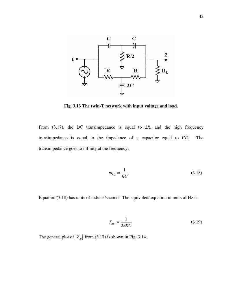
Fig. 3.13 The twin-T network with input voltage and load.
From (3.17), the DC transimpedance is equal to 2R, and the high frequency
transimpedance is equal to the impedance of a capacitor equal to C/2. The
transimpedance goes to infinity at the frequency:
RCRC
1=ω (3.18)
Equation (3.18) has units of radians/second. The equivalent equation in units of Hz is:
RCf RC π2
1= (3.19)
The general plot of mZ from (3.17) is shown in Fig. 3.14.

33
Fig. 3.14 The magnitude transimpedance of the twin-T network.
To gain an intuitive understanding of the twin-T, one must realize that the notch
effect of the twin-T network is based on the principle of phase cancellation. As long as
the values and ratios of R and C are precise, the AC current phase difference through
each path at the output is always equal to 180°. The CRC path behaves as a high-pass
filter and the RCR path as a low-pass. At the frequency in which their magnitudes are
equal, the currents cancel each other out completely and no current flows to the load.
Fig. 3.15 shows the output current magnitude through each branch on a log-scale plot
and the point at which the magnitudes are equal. Fig. 3.16 shows that the AC current
phase difference of the two paths is a constant 180° at all frequencies.

34
Fig. 3.15 AC output current magnitude of each branch of the twin-T network.
Fig. 3.16 AC output current phase of each branch of the twin-T network.

35
The absolute values of R and C in the twin-T network are not highly sensitive
parameters, as they mostly influence the filter in the asymptotic regions as was shown in
Fig. 3.14. In Fig. 3.17, a logarithmic sweep of R and C is shown for a constant RC
product. Notice that the notch frequency is not affected, even as R and C are swept over
2 orders of magnitude.
Fig. 3.17 Twin-T transimpedance for a sweep of R and C when RC product is fixed.
On the other hand, the precision of the component matching is very important to
the notch functionality of the twin-T because of the constant phase difference
requirement. As a consequence of the topology of the twin-T, the phase difference at
frequency extremes always approaches 180°, no matter what the component values are.
Unfortunately, the notch occurs at the midpoint of the phase change, which is also when
the rate of change is the highest. Thus any variation in the phase plot of either branch

36
will result in a large deviation from the constant 180° difference at the intended notch
frequency. Fig. 3.18 shows the deviation in output AC current phase through the RCR
branch when one of the resistors is varied by 10%, 25%, and 50%.
Fig. 3.18 RCR output current phase deviation for mismatch in one resistor.
Fig. 3.19 shows on a log-scale how the phase deviation from Fig. 3.18 affects the
response of the overall network. Notice that the notch depth is severely reduced with
only 10% mismatch in one component. At 50% mismatch, the notch is hardly present,
and the local minimum drifts to higher frequencies.

37
Fig. 3.19 Twin-T AC output current for mismatch in one resistor.
3.3 Design of the Improved Transimpedance Filter
The notch that is created by the twin-T network is useful for creating a locally
sharp change in AC response without the need for high order filters. This characteristic
is utilized in an active network to create an impedance shaper that can improve the
rejection of the existing TIA low-pass filter utilized in [4]. The concept of the current
divider, illustrated earlier in Fig. 3.2, is the basis of the improved filter design.
The proposed baseband transimpedance filter design achieves extra attenuation
of interfering signals near the edge of an existing filter’s bandwidth. The new filter is
placed in parallel with the existing single-pole low-pass transimpedance filter as shown
in Fig. 3.20.

38
Fig. 3.20 Existing transimpedance filter shown on the left hand side. On the right is the proposed additional filter, an impedance scaler for which Zi >> Zi,TIA for in-
band frequencies and Zi << Zi,TIA in the stop-band. The ideal shape of Zi is that of a low-pass notch where the notch is generated by the twin-T RC feedback network
and is designed to give sharp roll-off in the stop-band.
The new filter is designed to have relatively large impedance within the
bandwidth, but quickly change to low impedance in the stop-band; thus it diverts high
frequency current signals away from the main filter. The impedance of the additional
filter is shaped around a real capacitor Cfb. The impedance of the capacitor Cfb should be
significantly larger than the in-band TIA input impedance Zi,TIA to avoid attenuation of
desired signals. Just beyond the edge of the pass-band, Cfb is effectively multiplied to a
value such that it has much lower impedance than the out-of-band Zi,TIA.

39
The additional filter’s amplifier, which does the scaling, must have a large
enough GBW so that it has sufficient gain in the stop-band of interest (i.e. up to a certain
frequency, at which point a real capacitor such as Chf in Fig. 3.20). There is no
maximum requirement on the existing TIA op amp bandwidth, and the minimum
bandwidth is set by requirements for mixer linearity. The TIA gain-bandwidth product,
which determines Zi,TIA,, sets a maximum value on the low-frequency scaled Cfb. The
minimum Cfb is set by the largest anticipated interfering current signal and the available
voltage swing. Once Cfb is chosen, the optimum values of Cin, C, R, and Cx can be
selected.
3.3.1 Design Procedure
3.3.1.1 The Minimum Value for Cfb
Interfering current signals are filtered out by sinking them through Cfb. The
lowest-frequency interferer to be rejected and its largest anticipated value determine the
minimum value for Cfb. For a given voltage swing Vsw and interferer amplitude Iint at
frequency �int, the minimum value for Cfb can be determined by the following equation:
swfb V
IC
int
intmin, ω
= (3.20)
For example, for a 50 MHz 10 mA interferer and a maximum voltage swing of 1 V, the
smallest Cfb is roughly 32 pF. Chip area limitations may force the designer to use Cfb,min

40
for the value for Cfb. However, if area can be spared, it may be helpful to increase Cfb
beyond Cfb,min to relax the required values of other components and the specifications of
the filter amplifier. The maximum value for Cfb to avoid any attenuation of in-band
signals is discussed in the next design step. However, for very fast technologies which
have very low Zi,TIA up to the edge of the pass-band, the maximum value of Cfb can range
anywhere from 100 pF to greater than 1 nF. These values are generally considered too
large to design on-chip anyway.
3.3.1.2 The Ratios Cx to C, Cin to C, and the Product RC
The impedance Zi is shaped by using Cfb to close the loop around a high pass
filter. The closed loop impedance is given by the general equation:
( )sH
sCZ fb
i −≈
1
1
(3.21)
Equation (3.21) is a specific case of the general impedance transformation function
found in equation (3.2). H(s) is the filter’s open loop voltage transfer function when Cfb
is not present. In this design, H(s) has a high pass characteristic with a spike and is
calculated in Appendix B. The high-pass spike causes the shape of Zi to look like a low-
pass notch which is designed to give sharp roll-off of the input impedance just beyond
the edge of the pass-band. The impedance transfer function Zi is:

41
( )( )( )( ) ( )( ) ( )( )1222
12223
22
+++++++=
NCsCCNRCsCCNCCCRsRCs
Zfbxfbxfb
i (3.22)
where the notch frequency is determined by the twin-T RC product and is found in
equations (3.18) and (3.19), and where:
x
in
CC
N = (3.23)
Note that the notch frequency in (3.18) and (3.19) is only accurate if the additional filter
amplifier has high gain over all frequencies. In reality, as the amplifier gain reduces
because of bandwidth limitations, the actual location of the notch (or local minimum)
tends to drift to lower frequencies than fRC. This effect can be compensated for by
preemptively increasing the value of fRC.
Equation (3.23) is the factor by which Cfb is multiplied at low frequencies; that is,
Cfb,eff at low frequencies is equal to (N+1)Cfb. Thus, the impedance Zi for in-band
frequencies is given by the equation:
( ) fblfi CNs
Z1
1, +
= (3.24)
The value of Zi,lf in (3.24) must be at least 10 times larger than the largest in-band value
of Zi,TIA to avoid attenuation of desired signals. The graph in Fig. 3.1 shows Zi,TIA for

42
various TIA GBW. Once the largest in-band value of ZTIA is determined, Cfb and N
should be selected so that Zi,lf is much larger than ZTIA at the edge of the pass-band. For
example, for GBW = 1 GHz from Fig. 3.1, the input impedance around 10 MHz is about
7 �. This means the impedance of Zi,lf should be at least 70 � at 10 MHz. As a result,
the maximum allowable Cfb,eff is about 225 pF. For a minimum Cfb = 32 pF from the
example in the first design step, the maximum value for N is roughly 7.
From (3.22) it can be shown that the high frequency impedance Zi,hf is:
( ) fbhfi CMNs
Z21
1, ++
= (3.25)
where:
CC
M in= (3.26)
Observing (3.25) reveals that the effective capacitance Cfb,eff at high frequencies is equal
to Cfb(1+N+2M). From the standpoint of large rejection and low overall input
impedance Zi,tot, it is desirable to have a large value for (1+N+2M) in (3.25). However,
transient effects like ringing and overshoot, as well as the noise of resistors in the twin-T
network must also be taken into consideration when determining N and M. These effects
are highlighted in the next design step.

43
3.3.1.3 The Values Cx, Cin, C, and R
The absolute values of the components are relevant when considering noise, area
consumption, and power efficiency. The resistors in the twin-T network add noise
which is fed back to the TIA input through the relatively large capacitor Cfb. Minimizing
R can reduce in-band noise contribution, but there are a number of things to consider
when decreasing the value of R. First, small resistor values require the capacitors C, Cx,
and Cin to increase and so consume larger area. Second, as R gets smaller, perhaps in the
range of 100 � to 1 k�, the noise contribution of the new filter block may be dominated
by the noise of the filter amplifier rather than the resistors. Finally, as R gets smaller and
the capacitors get larger, more current must be fed back through the twin-T network and
Cx, causing the filter consume more power and operate less efficiently.
3.3.1.4 The Optimum Value of CTIA
It is observed that the additional filter produces bandwidth extension, with the
new -3 dB frequency occurring as high as twice the original bandwidth. This extended
bandwidth may be undesirable, and the simplest solution is to slightly decrease the pole
frequency in the TIA feedback. In the following macromodel design simulations, the
feedback capacitor CTIA is increased from 15.91 pF to 20 pF. This moves the real pole in
the TIA feedback from 10 MHz down to about 8 MHz, but keeps the actual -3 dB
bandwidth of the overall filter at 10 MHz.

44
3.3.2 Macromodel Simulation Results
The design procedure is now used to design filters for advanced processes, and
then the circuits are simulated using macromodel amplifiers. Macromodels are useful
for approximating the first order response of amplifiers designed in any technology.
Three different macromodel circuits are simulated and the results are shown on the
following pages. The component values used are summarized in Table 3.1.
The first macromodel amplifier has GBW = 1 GHz. In this circuit, the amplifier
specifications are relaxed for a 90 nm process. The gain bandwidth products of both the
TIA and additional filter amplifiers are set to GBW = 1 GHz with a DC gain Av = 1000
and one parasitic pole at fp = 1 MHz.
The second macromodel has GBW = 3 GHz. In this circuit, the amplifier
specifications match approximately what is reported for a 90 nm process [4]. The gain
bandwidth products of both the TIA and additional filter amplifiers are set to GBW = 3
GHz with a DC gain Av = 3000 and one parasitic pole at fp = 1 MHz.
Finally, the last macromodel has GBW = 5 GHz. In this circuit, the amplifier
specifications anticipate what may be achievable in advanced processes beyond 90 nm.
The gain bandwidth products of both the TIA and additional filter amplifiers are set to
GBW = 5 GHz with a DC gain Av = 5000 and one parasitic pole at fp = 1 MHz.

45
Table 3.1 – Summary of Components in Macromodel Simulations.
GBW 1 GHz 3 GHz 5 GHz DC Gain 1000 3000 5000 R 500 � 500 � 500 � C 3.54 pF 3.74 pF 3.74 pF Cin 4 pF 3.5 pF 3 pF Cx 650 fF 200 fF 100 fF Cfb 35 pF 40 pF 45 pF CTIA 20 pF 20 pF 20 pF
Macromodel simulations are of transimpedance gain (Fig. 3.21), total filter input
impedance (Fig. 3.22), and transient step response (Fig. 3.23).
Fig. 3.21 Transimpedance gain. Rejection is slightly improved for larger GBW. Better rejection (but higher noise) could be achieved by increasing Cfb. For the cases where GBW = 3 GHz and GBW = 5 GHz, the value of fRC = 85 MHz. For
GBW = 1 GHz, fRC = 90 MHz.

46
Fig. 3.22 Total filter input impedance Zi,tot. Overall input impedance is reduced for
larger GBW.
Fig. 3.23 Transient response to 1 mA current step for all three GBW. There is
slight ringing in all cases. Settling time for each is around 90 ns.

47
Figs. 3.24 – 3.26 show how fRC and component values are determined for the case where
the amplifier GBW = 3 GHz.
. Fig. 3.24 Transimpedance gain for GBW = 3 GHz. Sweep of fRC with appropriate
values of Cin and Cx to give small transient ringing while still attaining large rejection. Values of fRC are 65 MHz, 85 MHz, and 110 MHz. Sharper roll-off is achieved for smaller fRC but the attenuation at and just after the notch is worse.
Smooth transient response is also more difficult to achieve as fRC is reduced. Notice that the actual position of the notch occurs at lower frequencies than fRC (in this
case at 39 MHz, 50 MHz, and 64 MHz).

48
Fig. 3.25 Total filter input impedance Zi,tot for fRC = 65 MHz, 85 MHz, and 110
MHz. GBW = 3 GHz.
Fig. 3.26 Step response for GBW = 3 GHz. In all three cases, slight ringing is found
in the step response with fRC = 65 MHz showing the most, and fRC = 110 MHz showing the least. For fRC = 85 MHz and fRC = 110 MHz, the settling time is about
90 ns, and for fRC = 65 MHz, the settling time is around 120 ns.

49
CHAPTER IV
TRANSISTOR LEVEL DESIGN
The macromodel simulations presented in the previous chapter approximate how
the filter may operate in advanced technologies. But the single-pole amplifier
macromodels are very simplistic and do not take into account many real effects such as
non-dominant poles, output resistance, and slewing. The only way to accurately
determine the impact of these higher-order effects on the filter is to design and fabricate
the transistor level circuit. The final circuit in this thesis is designed and laid out in Jazz
Semiconductor 0.18 �m CMOS process, but an initial design has been done in TSMC
0.18 �m. Simulation results from both processes are included in this chapter. Both of
these processes are twice the size of the 90 nm process used in [4]. Therefore, it is
naturally expected that the amplifiers in 0.18 �m technology will have lower GBW, and
thus larger TIA input impedance, than what can be achieved in a 90 nm process.
4.1 Higher Order Effects
In the transistor level simulations, zeros in the transimpedance AC response,
which are due to finite bandwidth and output resistance of both the TIA and filter
amplifiers, cause a spike at around 1 GHz. To alleviate this problem without adding
complexity to the amplifiers, a small resistor Rfb is placed in series with the feedback
capacitor Cfb and another small resistor Rz is placed in series with CTIA. The effect of
these components is to smooth out the high frequency AC response. To show how a

50
resistor in series with the capacitor can help the circuit, a sweep of Rz is performed on a
macromodel circuit that includes amplifier output resistance. For simplicity, only the
original 10 MHz TIA filter is present, as shown in Fig. 4.1. The values used in the
simulation are Chf = 1 pF, Ro = 20 �, RTIA = 1 k�, and CTIA = 15.91 pF with Rz swept
from 1 � to 1 k� in one decade steps. Amplifier gain and bandwidth values are shown
in Fig. 4.1. Fig. 4.2 illustrates the effect of the series resistor Rz.
Fig. 4.1 Effect of the zero created by Ro, dampened by Rz.

51
Fig. 4.2 Sweep of Rz for the circuit in Fig. 4.1.
It is observed from Fig. 4.2 that there is a crossover frequency at which point Rz
has no effect on the gain. At frequencies higher than the crossover, Rz increases
attenuation, while at frequencies between the 10 MHz pole and the crossover point, Rz
has the undesirable effect of reducing the filter rejection. As Rz is increased at first, it
greatly improves the high frequency rejection while only slightly reducing the
attenuation at middle frequencies. However, as Rz gets even larger, it severely reduces
the attenuation between the 10 MHz bandwidth and the crossover frequency. Since
there is a trade-off for increasing Rz, it is up to the designer to determine its optimum
value.
In addition to series resistors, another way to help improve attenuation at high
frequencies is to increase the size of the capacitor Chf. Figs. 4.3 and 4.4 show the
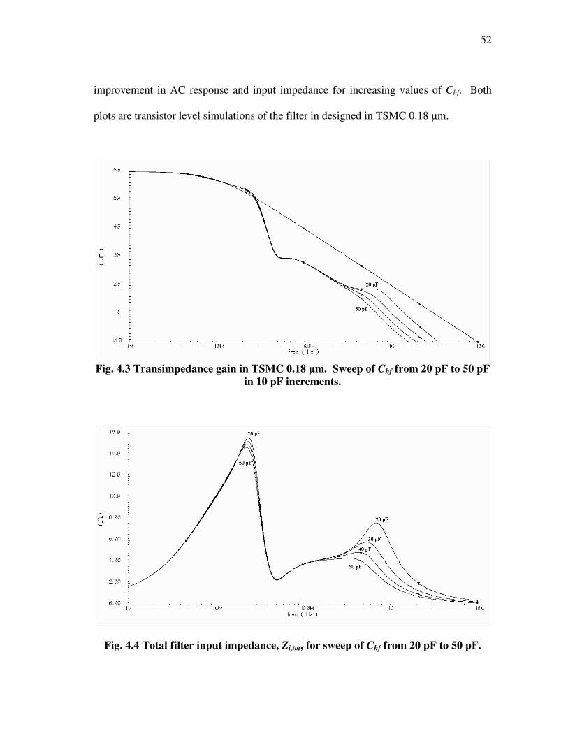
52
improvement in AC response and input impedance for increasing values of Chf. Both
plots are transistor level simulations of the filter in designed in TSMC 0.18 �m.
Fig. 4.3 Transimpedance gain in TSMC 0.18 �m. Sweep of Chf from 20 pF to 50 pF
in 10 pF increments.
Fig. 4.4 Total filter input impedance, Zi,tot, for sweep of Chf from 20 pF to 50 pF.

53
Note that in Fig. 4.3, the response is nearly the same for all values of Chf until
around 300 MHz. At this point the larger capacitor has better attenuation and a flatter
response. In Fig. 4.4, larger capacitor size slightly reduces input impedance around 20
MHz, but a much larger reduction is observed between 400 MHz and 2 GHz. From
these plots, the designer must decide the trade-off between added area consumption and
better high frequency attenuation. These changes in Chf have a negligible effect on filter
linearity or in-band noise.
4.2 Filter Design
The filter topology shown in Fig. 3.20 is designed in the transistor level. The
design procedure previously outlined is used to determine optimum component values.
The first step is determining Cfb. The absolute maximum voltage swing Vsw is equal to
the 1.8 V supply voltage, and the largest expected interferer Iint is about 10 mA. At the
very least, the filter should be able to process Iint at 50 MHz. From equation (3.20), the
smallest feedback capacitor Cfb is 17.7 pF. While selecting this value minimizes the area
consumption of the filter, a linear rail-to-rail filter output stage is necessary to handle the
large voltage swing required on Cfb, and it is not at all possible to filter Iint at any
frequency below 50 MHz. If however, Cfb is chosen so that only half the supply voltage
is used for the output voltage swing (Vsw = 0.9 V), then the minimum Cfb is about 35 pF.
Choosing the larger Cfb value does increase area consumption, but it enables much more
relaxed specifications for the filter amplifier’s output stage. Lower voltage swing
usually increases the linearity of the amplifier as well. Larger Cfb also makes it possible

54
to reject even lower frequency interferers. For example, if Cfb is 35 pF, then the Vsw
required to reject a 10 mA 40 MHz interferer is 1.14 V. For a 10 mA 30 MHz interferer,
Vsw is still only 1.5 V. This means it is possible to filter both of these frequencies, given
the 1.8 V supply.
The second step is to determine the component ratios. The notch frequency fRC
of the twin-T circuit should be higher than the actual desired notch point because the
finite bandwidth of the filter amplifier tends to make the notch or local minimum drift to
lower frequencies. This effect is visible in Fig. 3.24. The best way to determine fRC is to
run a parametric sweep of the twin-T RC product. Similar sweeps should be run to
determine the optimum values of N (3.23) and M (3.26).
To determine the absolute values of the components, it is necessary to balance
the trade-off of added noise as the twin-T resistors increase with the added power
consumption and rising capacitor area as the resistors decrease. Once the circuit is
designed up to this point and the frequency response in the range of 10 MHz to 100 MHz
is acceptable, attention should be paid to the circuit response at high frequencies. Rfb, Rz,
and Chf can be increased to compensate for any peaking or reduction in the roll-off. Fig.
4.5 shows the component values used in the design of the circuit in Jazz 0.18 �m.
Once the passive component values are determined, the last step is to design the
TIA amplifier and the filter amplifier. The following sections outline the design,
topology, and specifications of the transistor amplifiers.

55
Fig. 4.5 Filter with component values.
4.2.1 Filter Op Amp Folded-Cascode Gain Stage
The filter op amp is a two-stage amplifier consisting of a single gain stage and an
output buffer. The buffer will be required to handle the large 10 mA interferers.
Because of the inclusion of the buffer in the filter amplifier, only one gain stage is used
to conserve power. The gain stage does not necessarily need to have an extremely large
DC gain since its only function is to operate at frequencies greater than 10 MHz.

56
Instead, the main requirement of the filter amplifier is to have a large GBW, such that it
has reasonably high gain at very high frequencies.
A simple single gain stage op amp is the NMOS differential pair with active
PMOS load. The fully differential version of this circuit is shown in Fig. 4.6. The
differential pair is symmetrical around the vertical center; that is, M1 = M2 and M3 =
M4 in terms of size and DC bias.
Fig. 4.6 Simple NMOS differential pair with fully-differential PMOS load.
The DC differential voltage gain of the differential pair is:
omvo rgA 1−= (4.1)

57
where the output resistance ro is given by:
31
1
dsdso gg
r+
= (4.2)
The dominant pole in the differential pair is generally located at the output node. The
pole at this node is given by:
eqoutodB Cr ,
3
1=−ω (4.3)
where:
3311, gddbgddbeqout CCCCC +++≈ (4.4)
Equation (4.1) suggests that since the voltage gain of the differential pair is directly
proportional to the output resistance, increasing ro will improve the operation of the
circuit. While increased output resistance improves the DC voltage gain, it does not
increase GBW because the location of the dominant pole is inversely proportional to ro
as shown in (4.3). In fact, GBW is just the product of equations (4.1) and (4.3):
outeq
m
Cg
GBW,
1= (4.5)

58
From (4.5), it is evident that the way to increase GBW is to either reduce the equivalent
output capacitance Cout,eq or increase the input transistor transconductance gm1.
Generally for a simple differential pair, the bandwidth found in equation (4.3) can be
very large because the output resistance and capacitance are both relatively small.
The voltage headroom at the output of the simple differential pair is fairly large.
It is limited only by the overdrive voltages of the three vertical transistors. The voltage
headroom of the differential pair is given by:
( ) ( )9,3,1, DSATDSATDSATSSDDhr VVVVVV ++−−= (4.6)
Though the simple differential pair has a large bandwidth, it may not provide
enough gain for the filter to function properly. As observed from (4.1) and (4.5), higher
output resistance can increase gain without affecting GBW. High gain can be achieved
in one stage by using a cascode topology [6]. Fig. 4.7 shows a telescopic cascode
circuit. The approximate output resistance and capacitance of the cascode circuit are
given by the equations:
���
����
�++��
�
����
�++≈
75
5
7531
3
31,
11||
11
dsds
m
dsdsdsds
m
dsdscaso gg
ggggg
ggg
r (4.7)
3355, gddbgddbeqout CCCCC +++≈ (4.8)

59
Fig. 4.7 Fully differential cascode op amp.
The voltage gain of the cascode amplifier is improved over that of the simple differential
pair because the output resistance from (4.7) is much larger than ro found in (4.2). The
main disadvantage of the telescopic cascode amplifier is its reduced voltage headroom.
The output headroom of the amplifier in Fig. 4.7 is:
( ) ( )9,7,5,3,1,, DSATDSATDSATDSATDSATSSDDcashr VVVVVVVV ++++−−= (4.9)

60
Improved voltage swing can be realized with the folded-cascode topology, shown
in Fig. 4.8. From equation (3.20), large voltage headroom is important for keeping the
size of Cfb reasonably small. The gain, output resistance, and bandwidth of the folded-
cascode amplifier are the same as that of the telescopic cascode. The voltage headroom
of the folded-cascode op amp is increased by one overdrive voltage over the telescopic
cascode:
( ) ( )9,3,5,7,, DSATDSATDSATDSATSSDDfchr VVVVVVV +++−−= (4.10)
Fig. 4.8 Fully differential folded-cascode op amp.

61
Assuming the dominant pole of the filter op amp is located at the folded-cascode
output, the stability of the circuit can be controlled by placing a small capacitor Cc
between the amplifier output nodes as shown in Fig. 4.9. The effect of Cc is to increase
the equivalent capacitance at the output node. The equivalent output capacitance
becomes:
cgddbgddbeqout CCCCCC 23355, ++++≈ (4.11)
Fig. 4.9 Fully differential folded-cascode op amp with compensation.

62
Because of its high gain and reasonable output voltage swing, the folded-cascode
amplifier is utilized as the gain stage of the filter op amp. Bias voltages Vb1, Vb2, Vb4,
and Vb5 are generated by DC current mirrors, while Vb3 is controlled by a common mode
feedback circuit. Table 4.1 lists the capacitor value and the dimensions, overdrive
voltage, and bias current of each transistor in the folded-cascode amplifier.
Table 4.1 – Folded Cascode Component Operating Points.
Transistor/ Capacitor
Width [�m]/ Capacitance [pF]
Length [�m]
VDSAT [mV]
Ibias [mA]
M1 180 0.2 94.7 1.62 M2 180 0.2 94.7 1.62 M3 400 0.2 -149 2.35 M4 400 0.2 -149 2.35 M5 180 0.2 114 2.35 M6 180 0.2 114 2.35 M7 180 0.2 110 2.35 M8 180 0.2 110 2.35 M9 800 0.2 -136 3.98
M10 800 0.2 -136 3.98 M11 360 0.2 99.3 3.25 Cc 0.61 - - -
Because the folded-cascode circuit is fully differential and contains a high
impedance output node, it requires a common mode feedback (CMFB) error amplifier to
maintain a proper bias. Without a CMFB circuit, slight mismatch between the operating
points of the NMOS and PMOS transistors could force either the top or bottom half of
the circuit into the triode region. The basic CMFB circuit is composed of a common
mode detection circuit, reference voltage detection, and feedback to a controlling node in

63
the fully differential amplifier. Fig. 4.10 shows a low distortion CMFB topology used to
bias the folded-cascode stage:
Fig. 4.10 CMFB common-mode detector and error amplifier.
This topology similar to one proposed in [7]. The common mode output voltage is
detected by M1 and M2 and the reference voltage is detected by M3 and M4. The diode
connected load M5 returns the CMFB control signal to the folded cascode at the node
Vb3. The current sources M7 and M8 share the same bias voltage as the M9 and M10
from the folded-cascode amplifier, thus eliminating the need for an extra current mirror.
Table 4.2 shows the CMFB transistor dimensions and operating points.

64
Table 4.2 – Folded Cascode CMFB Transistor Operating Points.
Transistor Width [�m] Length [�m] VDSAT [mV] Ibias [mA] M1 400 0.2 -92.7 0.783 M2 400 0.2 -94.3 0.820 M3 400 0.2 -105 1.09 M4 400 0.2 -104 1.05 M5 160 0.2 111 2.14 M6 160 0.2 100 1.60 M7 400 0.2 -134 1.87 M8 400 0.2 -134 1.87
4.2.2 Filter Op Amp Class AB Output Buffer
The folded-cascode amplifier requires an output buffer for a couple of reasons.
The first is that if the large feedback capacitor Cfb is directly connected to the output
node, it would kill the bandwidth of the amplifier, rendering it useless for this high
frequency application. The second reason the amplifier requires a buffer is that even if it
could tolerate the reduced bandwidth caused by Cfb, it would not be able to supply the
current necessary to sink 10 mA interferers away from the TIA filter because its bias
current is not that large. Finally, even if its bias current were increased enough to
process a 10 mA signal, it would operate extremely inefficiently, requiring well over 10
mA DC bias current for both positive and negative output branches. The requirements
of the buffer then are to efficiently drive the feedback capacitor Cfb, introduce minimal
capacitance and conductance to the folded-cascode output nodes, and be very linear even
for large signals.

65
The selection of the class of amplifier for the buffer stage is very important. The
first thing to consider is the efficiency. The efficiency of an output stage is given as:
%100×=Dissipated
Load
PPη (4.12)
PLoad is the power delivered to the load and PDissipated is the average power consumed by
the buffer. Class A buffers, which operate with continuous current flow, achieve no
more than 25% efficiency. Class B buffers on the other hand, operate with no bias
current under quiescent conditions and only consume current when current is being
delivered to the load. A source-follower Class B buffer is shown in Fig. 4.11.
Fig. 4.11 Class B source-follower buffer.

66
Class B buffers can achieve maximum efficiency of 78.5%. Unfortunately, they
suffer from an effect called crossover distortion. Illustrated in Fig. 4.12, crossover
distortion is a result of both PMOS and NMOS transistors operating in the cutoff region
in the quiescent state. As the input voltage rises slightly, both transistors remain in
cutoff, causing no current to flow to the load. As the input voltage rises further such that
NTHoi Vvv ,>− , then the NMOS transistor turns on and current can flow to the load. The
same thing occurs to the PMOS device as the input voltage falls.
Fig. 4.12 Crossover distortion in class B buffer.
The class AB buffer is similar to the class B except that some bias current flows
in the quiescent state. This reduces the efficiency of the amplifier, but it eliminates the
crossover distortion. A source-follower class AB buffer is shown in Fig. 4.13. The

67
circuit is the same as the class B buffer except that gate voltage of the NMOS is shifted
up by a threshold voltage and the PMOS gate voltage is shifted down a threshold
voltage. This causes both transistors to operate at the edge of the saturation region.
Therefore any small change in input voltage causes current to flow to the load.
Fig. 4.13 Class AB source-follower buffer.
The common source buffer, shown in Fig. 4.14, is an alternative to the source-
follower buffer. The output resistance of the source-follower buffer is:
nmpm
sfo ggr
,,,
1+
= (4.13)
The output resistance of the common source buffer is:

68
ndspdscso gg
r,,
,
1+
= (4.14)
In general, the source-follower circuit has the benefit of lower output resistance than a
similar common source buffer. However, the common source buffer in Fig. 4.14 has a
number of advantages over the source-follower that make it desirable for use in this
application. First, the voltage headroom of the source-follower is reduced by the
threshold voltages of both the NMOS and PMOS, while the common source buffer is
only reduced by the overdrive voltages of its NMOS and PMOS. Second, for an N-well
technology, the source-follower NMOS transistor suffers from distortion due to the body
effect, whereas in the common source configuration, both transistors’ source-bulk
voltages are zero.
Fig. 4.14 Class AB common source buffer.

69
Fig. 4.15 shows a method for reducing the output resistance of the common
source buffer by using negative feedback error amplifiers to control the gate voltages of
the buffer transistors [8]:
Fig. 4.15 Buffer output resistance reduced by error amplifiers.
If each amplifier in Fig. 4.15 has a gain Av, the output resistance of the buffer is:
( )pmnmvndspdscsao ggAgg
r,,,,
,
1+++
= (4.15)
From (4.15) it is evident that large transconductance and amplifier gain significantly
reduce the output resistance of the amplifier. The amplifiers cannot just be designed

70
with high gain in mind. Since they are configured in closed loop with active transistors
which have gain of their own, the error amplifiers must also be carefully designed so as
to maintain loop stability. Therefore, an amplifier with moderate gain and high
bandwidth, such as a single-ended differential pair, is desired. Fig. 4.16 shows the
buffer schematic with error amplifiers.
Fig. 4.16 Output buffer with single-ended error amplifiers.

71
Two buffers, one for each output, are needed for the filter amplifier since it is a fully
differential circuit. This means a total of four error amplifiers are required, which could
consume a large amount of power unless the amplifiers are specifically designed for low
power operation. Table 4.3 shows the operating points of each device in Fig. 4.16.
Table 4.3 – Output Buffer Transistor Operating Points.
Transistor Width [�m] Length [�m] VDSAT [mV] Ibias [mA] M1 80 0.18 94.6 0.811 M2 80 0.18 91.0 0.761 M3 80 0.18 -170 0.811 M4 80 0.18 -167 0.761 M5 160 0.18 96.7 1.57 Mn 100 0.18 274 4.18 Mp 30 0.18 -339 4.12
4.2.3 TIA Op Amp
For a more consistent comparison between the operation of the original TIA filter
and the filter proposed in this thesis, the TIA amplifier is designed with the same
topology as in [4]. The op amp is a two stage fully-differential operational
transconductance amplifier (OTA) as shown in Fig. 4.17. The CMFB network in [4]
senses the common mode voltage at the output nodes and returns the common mode
control signal to node Vb2. The topology of the CMFB is not reported in [4], so the same
topology that was used for the filter amplifier CMFB is utilized for the TIA. The only
difference is that the common mode control voltage is taken from the drain of M6
instead of M5. The reason for this is that since the OTA in Fig. 4.17 has two gain stages,

72
there is one more inversion than in the filter amplifier. In order to keep the loop in
negative feedback, the output has to be taken at the other load transistor.
Fig. 4.17 Fully-differential OTA from [4].
Linearity of the amplifier is improved by making GBW large. Because of the
large GBW, non-dominant poles can cause stability problems. Miller capacitor Cc splits
the dominant and non-dominant poles to maintain good phase margin, and the resistor Rc
is used to cancel the feedforward zero created by Cc. While noise is not a concern in the
filter op amp because it only interacts with the filter in the stop-band, the TIA op amp

73
processes in-band signals and must therefore be a low noise device. In fact, because the
current mode passive mixer has such low flicker noise, the TIA op amp is the main
contributor of this low frequency noise. The input differential pair M1 and M2 is
composed of very large transistors to reduce flicker noise as much as possible [9].
Additionally, PMOS transistors are used because they have a lower flicker noise
coefficient. A summary of TIA op amp components is shown in Table 4.4. Common
mode feedback components are shown in Table 4.5.
Table 4.4 – TIA Component Operating Points.
Transistor/ Capacitor/ Resistor
Width [�m]/ Capacitance [pF]/
Resistance [�]
Length [�m]
VDSAT [mV]
Ibias [mA]
M1 432 0.18 -175 3.90 M2 432 0.18 -175 3.90 M3 432 0.18 -163 3.90 M4 432 0.18 -163 3.90 M5 240 0.18 112 3.90 M6 240 0.18 112 3.90 M7 240 0.18 122 4.41 M8 240 0.18 121 4.31 M9 240 0.18 119 4.41
M10 360 0.18 118 4.31 M11 360 0.18 -184 4.37 M12 360 0.18 -183 4.30 M13 810 0.18 -176 7.81 Cc 4 - - - Rc 50 - - -

74
Table 4.5 – TIA CMFB Transistor Operating Points.
Transistor Width [�m] Length [�m] VDSAT [mV] Ibias [mA] M1 180 0.18 -163 1.67 M2 180 0.18 -189 2.29 M3 180 0.18 -170 1.84 M4 180 0.18 -145 1.28 M5 252 0.18 102 3.12 M6 252 0.18 111 3.96 M7 360 0.18 -176 3.50 M8 360 0.18 -177 3.57
Table 4.6 is a summary of the specifications of the filter amplifier, including
folded-cascode gain stage with output buffer and the TIA amplifier.
Table 4.6 – Amplifier Specifications.
Specification Filter Amplifier TIA Amplifier Current Consumption 56 mA 24.7 mA DC Gain 43.5 dB 53 dB GBW 882 MHz 1.02 GHz Phase Margin 49° 71.5° Buffer Output Resistance 5 � up to 1 GHz N/A Settling Time 110 ns 80 ns
4.3 Layout Considerations
Ideally, the fabricated circuit should show the same response as the schematic
level design. Unfortunately, parasitics such as substrate capacitance and metal trace
resistance can cause significant worsening of the response, especially at high
frequencies. The layout of the circuit must be carefully designed to reduce parasitics and
to ensure good matching of differential components. Interconnecting blocks are placed

75
physically close to each other to minimize metal trace length. Also, metal wires
conducting large currents such as power supply connections are made wide to reduce
current density and resistive voltage drop, whereas wires carrying small bias currents
and high frequency signals are made narrow to reduce the metal-to-substrate
capacitance.
4.3.1 Passive Components
Common centroid techniques are employed on differential components where
possible. Capacitors are broken up into fractions and then interspersed in a checkered
fashion with similar capacitors. For example, there are two 35 pF capacitors Cfb in the
filter. Each Cfb is broken up into 8 different 4.375 pF capacitors and then combined with
the other Cfb as shown in Fig. 4.18. This technique minimizes mismatch due to gradients
on the surface of the wafer. All capacitors in this filter design that have a matching
component utilize the common centroid technique.
Fig. 4.18 Capacitors with common centroid.

76
Resistors generally consume much smaller area than capacitors, which means
surface gradients tend to affect them with less intensity. Instead of using the common
centroid technique, matching resistors are simply placed directly adjacent to each other
and in the same orientation. This provides good matching without increasing the
complexity of the resistor layout.
4.3.2 Active Components
For transistors, multi-finger design is used to reduce polysilicon gate resistance.
However, more fingers mean larger source/drain area and thus larger source-to-substrate
and drain-to-substrate parasitic capacitances. Therefore, a compromise can be reached
between gate resistance and substrate capacitance. Also, like the capacitors, common
centroid technique is used for matching transistors. In addition, dummy transistors are
used to reduce variation at the edges of the transistor blocks. Fig. 4.19 shows an
example of matching transistors. Each transistor M1 and M2 has a gate width of 3.6 �m
× 4 fingers × 2 multiplier = 28.8 �m. Where possible, transistors in the filter that have a
matching component utilize the common centroid technique and dummy transistors. All
transistors with widths larger than 10 �m are split into multi-finger devices.

77
Fig. 4.19 Multi-finger common centroid matched transistors with dummy elements.
To reduce the body effect, all PMOS devices are placed in an N-well biased to
the same potential as the transistor source terminal. This means matching PMOS
devices that do not share the source node cannot be made common centroid since they
must be in separate N-wells. The bulk nodes of all NMOS devices are connected to the
lowest supply potential and not the source nodes, so all NMOS devices utilize the
common centroid technique.
4.3.3 Chip Layout
The overall layout of the chip is shown in Fig. 4.20. The upper portion of the
layout is the original TIA filter combined with the filter proposed in this thesis. Below it
is the original TIA filter without the proposed filter. Both versions of the filter are

78
included on the test chip so that fair testing and analysis can be done on the chip after
fabrication.
Fig. 4.20 Filter layout in Jazz 0.18 �m.

79
CHAPTER V
SIMULATION RESULTS
The results of the designed filter designed in Jazz 0.18 �m are compared with
those of the original TIA filter also designed in Jazz 0.18 �m. Where applicable, these
results are also compared with the ideal single-pole low-pass transfer function.
5.1 Schematic Level Simulation Results
Fig. 5.1 shows the AC response of the designed filter along with the original
filter and the single pole low-pass transfer function. As expected in the new filter, slight
bandwidth extension occurs up to about 20 MHz at which point the filter response
quickly falls to below 30 dB for the rest of the frequency spectrum. In the final
schematic level design, the series feedback resistor Rfb is designed to be 5 � instead of
10 � because it is expected that in the layout of the circuit the wire traces will add extra
series resistance which will degrade the circuit performance in the lower stop-band
frequencies. The trade-off is that the schematic level simulation includes the large bump
in response around 900 MHz. The consequence of this bump is increased input
resistance and lost rejection at high frequencies. It does not significantly affect stability
or transient response.

80
Fig. 5.1 AC response of filter.
Fig. 5.2 shows the small signal input impedance of the filter. The input
impedance remains below 15 � over all frequencies and below 8 � in the high
frequency stop-band. Most importantly, the input impedance between 40 MHz and 400
MHz is kept well below 4 �, which is very low. While the 13 � peak input impedance
of the original filter is lower than that of the new filter, the original filter input
impedance is at this peak throughout the critical 40 MHz to 400 MHz range. It is in the
range that large interferers threaten the linearity of the filter.
Fig. 5.3 is the transient response to a 1 mA input current pulse. Slight ringing in
the new filter is observed due to the additional filter network, while the original filter
shows a first order response. The ringing in the new filter is expected and was observed
in the macromodel simulations.

81
Fig. 5.2 Small signal input impedance of filter.
Fig. 5.3 Filter transient response to 1 mA current pulse.

82
Fig. 5.4 shows the transient response of the new filter to a 10 MHz 100 �A signal
along with a 50 MHz 1 mA interferer, and Fig. 5.5 shows the response of the original
filter to the same 10 MHz signal and 1 mA 50 MHz interferer.
Fig. 5.4 New filter response to 10 MHz 100 �A and 50 MHz 1 mA signals.

83
Fig. 5.5 Original filter response to 10 MHz 100 �A and 50 MHz 1 mA signals.
Fig. 5.6 and Fig. 5.7 show the responses to 10 MHz 100 �A and 50 MHz 10 mA
signals of the new and original filters, respectively. Notice that the 0-to-peak voltage of
the 50 MHz signal for the new filter is around 350 mV, whereas the 0-to-peak voltage of
original filter is 1.6 V. Fortunately, the supply voltage for Jazz 0.18 �m is 1.8 V so this
signal does not saturate the TIA filter, but if the supply was 1 V, then the filter would be
very saturated.

84
Fig. 5.6 New filter response to 10 MHz 100 �A and 50 MHz 10 mA signals.
Fig. 5.7 Original filter response to 10 MHz 100 �A and 50 MHz 10 mA signals.

85
Fig. 5.8 and Fig. 5.9 show the discrete Fourier transform (DFT) of the waveform in Figs.
5.6 and 5.7, respectively. The DFT window is rectangular with a width of 500 ns, and N
= 512 samples. A comparison of Figs. 5.8 and 5.9 shows that the 10 mA 50 MHz signal
response of the new filter is attenuated 12 dB more than the original filter. The new
filter also shows less harmonic distortion than the original filter. Notice on both plots
the intermodulation harmonics at 30 MHz, 70 MHz, 90 MHz, etc. The largest harmonic,
at 150 MHz, is 16 dB lower for the new filter. In any case, the 150 MHz harmonic is not
a big issue because it is far beyond the 10 MHz bandwidth and will be filtered by the
DSP.
Fig. 5.8 DFT for new filter 10 MHz 100 �A signal and 50 MHz 10 mA interferer.

86
Fig. 5.9 DFT for original filter 10 MHz 100 �A signal and 50 MHz 10 mA interferer.
The DFT of the response of the new filter to 50 MHz 5 mA and 90 MHz 5 mA signals is
shown in Fig. 5.10. The DFT window is rectangular with a width of 500 ns, and N =
512 samples. The concern with these two interferers is the intermodulation product 2f1 –
f2. For f1 = 50 MHz and f2 = 90 MHz, the result is 10 MHz. This in-band harmonic is
very problematic because it will not be filtered by the DSP. Comparing Figs. 5.10 and
5.11, the 10 MHz harmonic in the new filter response is nearly 10 dB below the 10 MHz
harmonic in the original filter. This result is due to the fact that the input impedance of
the original filter at these frequencies is much larger than the input impedance of the new
filter, so the voltage level at the amplifier inputs is much larger for the simple TIA filter.

87
Fig. 5.10 DFT of new filter response for 50 MHz and 90 MHz 5 mA signals.
Fig. 5.11 DFT of original filter response for 50 MHz and 90 MHz 5 mA signals.

88
Fig. 5.12 and Fig. 5.13 show the DFT of the new filter and original filter response to 9
MHz and 10 MHz 500 �A input signals. The DFT window is rectangular with a width
of 1 �s, and N = 512 samples. Intermodulation distortion is similar for both filters, and
in-band harmonics are at least 60 dB below the input tones.
Fig. 5.12 New filter DFT for 9 MHz and 10 MHz 500 �A signals.

89
Fig. 5.13 Original filter DFT for 9 MHz and 10 MHz 500 �A signals.
Fig. 5.14 shows the input referred spot noise current density for the new filter
and the original filter. The noise of the new filter is higher than the original, which is
expected since more circuitry has been added to the system. However, only the noise in
the 10 MHz bandwidth is of concern, so the large noise density of the new filter in the
stop-band does not pose a problem. In fact, Fig. 5.14 is only correct up to 10 MHz, since
at higher frequencies most of the input current noise is diverted into the new filter and
does not appear at the real output. The noise summary is shown in Table 5.1.
Table 5.1 – Noise Summary.
Filter Integrated Noise (1 kHz – 10 MHz) [nA] New Filter 211
Original Filter 58.9

90
Fig. 5.14 Input referred spot noise current density.
5.2 Post-Layout Simulation Results
Layout results are somewhat degraded from those of the schematic level
simulations. It is already very difficult to achieve GBW above 1 GHz in 0.18 �m
technology, but the bandwidth is further reduced by metal wire resistance and parasitic
capacitance. The AC plot is shown in Fig. 5.15. Rejection between 30 MHz and 300
MHz is up to 13 dB worse than in the schematic level. The response of the original filter
is also worse because of its limited bandwidth. Fig. 5.16 compares the small signal input
impedance of the new and old filters. The minimum input impedance of the improved
filter is 5.2 � compared to 1 � in pre-layout simulations.

91
Fig. 5.15 Post-layout AC simulation results.
Fig. 5.16 Post-layout small signal input impedance.

92
The transient step response to 1 mA current pulses is shown in Fig. 5.17. The ringing
that appeared in the pre-layout simulations of the improved filter is further dampened by
parasitics.
Fig. 5.17 Post-layout transient step response.
Figs. 5.18 and 5.19 show the transient response of the old and new filters to 10
MHz 100 �A and 50 MHz 1 mA inputs. While post-layout simulations show that the
rejection of the improved filter is not as good as the schematic level simulations in Fig.
5.4, it is still much better than the post-layout simulations of the old filter response in
Fig. 5.19.

93
Fig. 5.18 Post-layout transient response of new filter to 10 MHz 100 �A and 50 MHz 1 mA signals.
Fig. 5.19 Post-layout transient response of original filter to 10 MHz 100 �A and 50 MHz 1 mA signals.

94
To illustrate the impact of reduced input impedance, the input voltage waveforms
associated with Figs. 5.18 and 5.19 are displayed in Fig. 5.20. The larger input voltage
is indicative of larger input impedance. This larger voltage swing not only reduces the
linearity of the filter amplifiers, but it also decreases mixer channel resistance linearity.
Fig. 5.20 Transient input voltage waveform in the presence of 10 MHz 100 �A and 50 MHz 1 mA signals.
Figs. 5.21 and 5.22 show the transient response of the old and new filters to 10 MHz 100
�A and 50 MHz 10 mA inputs.

95
Fig. 5.21 Post-layout transient response of new filter to 10 MHz 100 �A and 50 MHz 10 mA signals.
Fig. 5.22 Post-layout transient response of original filter to 10 MHz 100 �A and 50 MHz 10 mA signals.

96
The frequency components of Figs. 5.21 and 5.22 are displayed in Figs 5.23 and
5.24, respectively. The DFT window is rectangular with a width of 500 ns, and N = 512
samples. The 50 MHz tone of the original filter response is about 7 dB larger than that
of the new filter.
Fig. 5.23 Post-layout DFT of response of new filter to 10 MHz 100 �A signal and 50 MHz 10 mA interferer.

97
Fig. 5.24 Post-layout DFT of response of original filter to 10 MHz 100 �A and 50
MHz 10 mA interferer.
Fig. 5.25 shows the input referred spot noise current density for the new filter
and the original filter. As in the pre-layout simulations, the noise of the new filter is
larger than the original. Also, Fig. 5.25 is only valid from 1 kHz to 10 MHz, since after
10 MHz, most of the input noise current is diverted to the new filter and does not show
up at the original filter output. The noise summary is shown in Table 5.2.
Table 5.2 – Post-Layout Noise Summary.
Filter Integrated Noise (1 kHz – 10 MHz) [nA] New Filter 242
Original Filter 56.3

98
Fig. 5.25 Post-layout simulation of input referred spot noise current density.

99
CHAPTER VI
CONCLUSION
In this thesis, an improved low-pass transimpedance filter is designed in Jazz
0.18 �m process. The original one-pole low pass filter from [4] is also designed in Jazz
0.18 �m, and the simulation results of both are compared. Since the input to a
transimpedance circuit is current, the designed filter utilizes the current divider concept
to attenuate stop-band interferers. The new circuit is placed in parallel with the existing
TIA filter and draws current signals away from the TIA filter by shaping a passive
impedance. The passive impedance is a large capacitor which is multiplied at high
frequencies by way of a sharp high pass filter. Capacitive multiplication is based on
Miller’s well-known theorem [5].
The existing one pole filter with 10 MHz bandwidth has less than 15 dB
attenuation of interferers at 50 MHz, which may not be enough to prevent the filter from
saturating if supply voltage is low and the interferer is very large. The designed filter
sinks the large interfering current away from the TIA filter which prevents saturation and
relaxes requirements on the digital filtering blocks. In schematic level simulations,
interferers at 40 MHz and 50 MHz are rejected by 30 dB and 35 dB, respectively. In
post-layout simulations, 40 MHz and 50 MHz attenuations are greater than 25 dB.
In addition to improved rejection, by sinking the large interferers away from the
filter, the voltage swing at the input, and thus in the input impedance, is significantly
reduced. Reduced input voltage swing increases the linearity of both the transimpedance

100
filter and the preceding mixer block. It has been shown that in-band intermodulation
harmonics can be reduced by 10 dB.
Improvements can be to the made to the filter as technology size is reduced.
Smaller parasitics increase the bandwidth of the new filter amplifier making it better able
to process large currents at higher frequencies. This will increase attenuation of stop-
band tones and reduce the overall filter input impedance.
Even if amplifiers with extremely high GBW are employed, there are still some
issues that arise because of the nature of the passive RC network which defines the filter
response. One disadvantage of the design in this thesis is the small ringing that is
observed in the transient step response. Another disadvantage is the large capacitor sizes
that must be used to meet the low-voltage high-current requirements of the receiver.
Finally, the power consumption of the filter amplifier is around twice that of the original
TIA. Increased power consumption is to be expected since the filter amplifier is
required to process much larger signals at much higher frequencies than the TIA.
However, future research should be devoted to finding improvements and solutions to
these drawbacks.

101
REFERENCES
[1] B. Razavi, RF Microelectronics, Upper Saddle River, NJ: Prentice Hall, 1998.
[2] J. Tsividis, Operation and Modeling of the MOS Transistors, 2nd ed., Boston,
MA: McGraw-Hill, 1999.
[3] S. Zhou and M.-C. F. Chang, “A CMOS passive mixer with low flicker noise for
low-power direct conversion receiver,” IEEE J. Solid-State Circuits, vol. 40, pp.
1084 – 1093, May 2005.
[4] J-H C. Zhan, B. R. Carlton, and S. S. Taylor, “A broadband low-cost direct-
conversion receiver front-end in 90 nm CMOS,” IEEE J. Solid-State Circuits,
vol. 43, pp. 1132 – 1137, May 2008.
[5] J. M. Miller, “Dependence of the input impedance of a three-electrode vacuum
tube upon the load in the plate circuit,” Scientific Papers of the Bureau of
Standards, vol. 15, pp. 367 – 385, 1920.
[6] B. Razavi, Design of Analog CMOS Integrated Circuits, New York: McGraw-
Hill, 2001.

102
[7] J. F. Duque-Carillo, “Control of the common-mode component in CMOS
continuous-time fully differential signal processing,” Analog Integrated Circuits
and Signal Processing, vol. 4, pp. 131 – 140, 1993.
[8] P. E. Allen and D. R. Holberg, CMOS Analog Circuit Design, New York: Oxford
University Press, 2nd ed., 2001.
[9] M. Valla, G. Montagna, R. Castello, R. Tonietto, and I. Bietti, “A 72-mW CMOS
802.11a direct conversion front-end with 3.5-dB NF and 200-kHz 1/f noise
corner,” IEEE J. Solid-State Circuits, vol. 40, pp. 970 – 977, April 2005.

103
APPENDIX A
ADDITIONAL TRANSIMPEDANCE AND INPUT IMPEDANCE EQUATIONS
The input impedance of the TIA block can be expressed by the following
equation:
( )( ) pvTIATIApvTIATIA
pTIATIAi ACRAsCRs
sRZ
ωωω
''2, 1 ++++
= (A.1)
where Av is the gain of the existing TIA op amp, vv AA += 1' , �p is the TIA op amp
dominant pole, and RTIA and CTIA are the feedback impedances. (It is assumed that the
first non-dominant pole is at much higher frequencies than �p and thus does not affect
Zi,TIA very much at frequencies below GBW). Then putting Zi,TIA in parallel with Zi
(3.21) gives the full equation for the total input impedance:
( ) ( )( )( )( )( )( )
( ) ( )( )( )
( ) ( )( )( )( )
pv
TIATIApvfbTIAp
fbTIAxTIApfbpvTIATIA
xfbTIA
xfbTIApTIATIApv
xfbTIATIA
ppTIAtoti
A
CRANCRs
NCRCCNRRCCRACRs
CCNCRR
CCNCCCRRCRACRs
CCNCCCCRRs
sCRsCRsRZ
ω
ωω
ωω
ωω
ωω
'
'
22'2
2'223
224
222223
,
11
122
22
21
2
+
++++
++++++
��
�
�
��
�
�
++
+++++
++++++
= (A.2)

104
Equation (A.2) represents the total input impedance Zi,tot neglecting Chf. The equation
for the overall transfer function is:
( )( ) ( ) ( )( )iTIAvTIAhfTIATIAv
TIAv
i
o
ZRARCCRAsRA
iv
+++++−=
11 (A.3)
where RTIA = 1 k�, CTIA = 15.91 pF and Av is the gain of the existing TIA op amp.
If ∞→vA , then (A.3) reduces to the expected first order equation:
( ) 1+−=
TIATIA
TIA
i
o
CRsR
iv
(A.4)
If the existing TIA’s dominant parasitic pole at �p is included, then equation (A.3)
becomes:
( )
( )
( ) ��
�
�
��
�
����
����
�+++
��
�
�
��
�
����
����
�+++++
��
�
�
��
�
�+
−=
i
TIAv
i
TIA
pTIAhfTIATIAv
TIAhfTIATIAp
TIAv
i
o
ZR
A
ZR
RCCRAs
RCCRs
RAiv
1
11
1
12
ω
ω
(A.5)
Putting (3.21) into (A.3) gives the following transimpedance transfer function:

105
( )( ) ( )( )( )( )
( )( ) ( )( )( )
( ) ( )( )
( )( )( )pv
fbTIATIAhfTIATIAvp
xfbTIAp
vpfbTIAhfTIATIA
xfbTIAp
xfbTIAhfTIATIAvp
xfbhfTIATIA
pTIAvpTIAv
i
o
A
NCRRCCRAs
CCNCRR
CRANCRCCRs
CCNCCCRR
CCNCRRCRCCRACRs
CCNCCCCCCRRs
RARACRs
iv
ω
ω
ωω
ω
ω
ωω
'
'
22'2
2
22'22
3
24
222
11
22
1
2
22
2
+++++
+��
�
�
��
�
�
++
++++
+��
�
�
��
�
�
+++
++++
++++++
−=
(A.6)
where N is found in (3.23) and:
vv AA += 1' (A.7)

106
APPENDIX B
OPEN LOOP TRANSFER FUNCTION OF AUXILIARY FILTER
The open loop transfer function of the circuit shown in Fig. B.1 is:
( ) ( )
( ) 1
22
2
222
22
+
+���
����
�++��
�
����
�+
−=CRs
CC
CCCRC
sCCC
CCRs
vv x
inx
x
inx
x
in
i
o (B.1)
Fig. B.1 Open loop high-pass filter with ideal amplifier.
Substituting N from (3.23) into (B.1), then the reduced equation is:

107
( )( ) ( )( )( ) 1
222222
22
+++++
−=CRs
NCCRNsCCCNRsvv xx
i
o (B.2)

108
APPENDIX C
PARAMETRIC, CORNER, MONTE CARLO, AND PARASITIC SIMULATIONS
All simulations in Appendix C were done on a circuit designed in TSMC 0.18
�m. Results show the impact of process and temperature variations on filter
performance.
Part 1: Parametric Sweeps
Fig. C.1 ±50 % variation in one R in twin-T (same R for both sides of differential
circuit).

109
Fig. C.2 ±50 % variation in one C in twin-T (same C for both sides of differential
circuit).
Fig. C.3 ±50 % variation in Cin (same for both sides of differential circuit).

110
Fig. C.4 ±50 % variation in Cx (same for both sides of differential circuit).
Fig. C.5 Variation in CC,TIA. Larger value reduces TIA bandwidth which increases
rejection.

111
Fig. C.6 Variation in CC,TIA. Larger value reduces TIA bandwidth which increases
circuit input impedance.
Fig. C.7 Variation in CC,FilterAmp. Larger value reduces filter amplifier bandwidth
which decreases rejection.

112
Fig. C.8 Variation in CC,FilterAmp.
In Fig. C.8, larger CC,FilterAmp reduces input impedance before “notch”, but
increases it after “notch”, though high frequency spike in impedance may occur for
small values if Chf is not large enough.

113
Part 2: Corner Simulations
Fig. C.9 AC results of corner simulations. Curves for fast/slow and slow/fast are run with nominal supply voltage and current and at T = 27°C. Fast/fast corner is run with 110% supply voltage and current and at T = -20°C. Slow/slow corner is
run with 90% supply voltage and current and at T = 60°C.
In Fig. C.9, the high frequency bump for the fast/slow corner does not have a
significant effect on transient response, but does reduce rejection and increase input
impedance. It can be improved with larger Chf as shown in Fig. C.10.

114
Fig. C.10 AC result for fast/slow corner and sweep of Chf. The high frequency bump
is reduced for larger Chf.
Fig. C.11 Input impedance corner simulations. Curves for fast/slow and slow/fast
are run with nominal supply voltage and current and at T = 27°C. Fast/fast corner is run with 110% supply voltage and current and at T = -20°C. Slow/slow corner is
run with 90% supply voltage and current and at T = 60°C. The slow/fast corner peaks at 18 �, and the slow/slow corner peaks at 28 �.

115
Part 3: Monte Carlo Simulations
Fig. C.12 Histogram showing filter rejection at 50 MHz. Average rejection (from
60 dB) is 29 dB with a standard deviation of 1.4 dB.
Fig. C.13 Histogram showing filter rejection at 75 MHz. Average rejection (from
60 dB) is 31 dB with a standard deviation of 0.3 dB.
116
Fig. C.14 Histogram showing filter rejection at 100 MHz. Average rejection (from
60 dB) is 32 dB with a standard deviation of 0.2 dB.
Fig. C.15 Histogram showing maximum input impedance. Average maximum
input impedance is 15.4 � with a standard deviation of less than 1 �.

117
Part 4: Parasitic Simulations
Grounded parasitic capacitors at each node are defined in terms of percent of the
total capacitance connected to that particular node. Sweeps are done from 1% to 100%.
From Fig. C.16, more parasitics reduce the rejection from edge of bandwidth up to about
300 MHz, at which point the parasitic capacitors tend to increase rejection.
Fig. C.16 Transimpedance gain for parasitic sweep.

118
Fig. C.17 Input impedance for parasitic sweep.
Fig. C.18 Transient step response for parasitic sweep.
In Fig. C.17, more parasitics reduce Zi from edge of bandwidth up to the notch,
increase Zi from notch to about 300 MHz, then once again reduce Zi. In Fig C.18, more

119
parasitics reduce ringing in the step response. Fig. C.19 shows more parasitics increase
in-band noise levels.
Fig. C.19 Input referred spot noise current for parasitic sweep.

120
VITA
Name: James Keith Hodgson
Address: Department of Electrical and Computer Engineering, Texas A&M University 214 Zachry Engineering Center TAMU 3128 College Station, TX 77843-3128 Email Address: [email protected] Education: B.S., Electrical Engineering, Texas A&M University, 2005 M.S., Electrical Engineering, Texas A&M University, 2009