design of 2.4ghz 5w rf power amplifier … transformation and biasing networks. ... cree transistor...
TRANSCRIPT
International Journal of Scientific & Engineering Research, Volume 5, Issue 4, April-2014 324 ISSN 2229-5518
IJSER © 2014 http://www.ijser.org
DESIGN OF 2.4GHz 5W RF POWER AMPLIFIER USING GaN TECHNOLOGY
A.Banu priya, M.H.Masood, Rajesh Kunnath
Abstract-This paper presents the design of RF Power amplifier for WLAN(Wireless Local Area Network) application is a challenging job as it is required to meet stringent specifications like stable Performance of the system, operate at temperature extremes and other mechanical aspects. For narrowband operation (2.3-2.9GHz), it is necessary to design RF Power Amplifier with optimal gain around 13dB. The RF Power Amplifier using CREE GaN technology designed specifically for high gain, high efficiency and wide bandwidth capabilities for wi-fi and wiMAX applications. It plays a major role in amplifying the required high frequency RF signal without distortions and other impairments which would decrease the usefulness of the signal. To address this, efforts has been made to design an RF power amplifier operating at 2.4GHz of frequency by using GaN technology by using ADS software. Index terms-power amplifier, Gallium Nitride HEMT, WLAN, ADS(Advanced Design System)software.
I.INTRODUCTION
The term power amplifier is a relative term with respect to the amount of power delivered to the load and/or sourced by the supply circuit. In general a power amplifier is designated as the last amplifier in a transmission chain (the output stage) and is the amplifier stage that typically requires most attention to power efficiency. Amplifier designed to attach to a transmission line at input and/or output deal with voltage or current individually, they ideally couple with an input and/or output impedance matched to the transmission line impedance. For a given appropriate source and load impedance, RF amplifier can be characterized as amplifying voltage or current, they are fundamentally amplifying power[3,4,8].
A technical definition for RF PA might be a circuit that is consuming DC power circuit in Order to deliver maximum RF/microwave output power. It consists of the transistor and matching parts for the input and output required for impedance transformation and biasing networks. The need for matching networks arises because, in amplifiers in order to deliver maximum power to a load or to perform in a certain desired way, must be terminated properly at both the input and output ports. Thus the maximum available power is delivered if the input matching network is
impedance matched with the output matching network.
The design of microwave amplifiers depends primarily on the terminal characteristics of the transistor. These are represented by means of the 2 port S-parameter of the device. The transistor is chosen based on the requirements. This active device is used to have an amplified input signal at the output depending on the specific requirements for the amplifier design. The Cree transistor model used in this allows having a broadband solution and operates from a 28 Volt rail with high efficiency[6,7,9].
II.SYSTEM MODEL
A.CREE TRANSISTOR
The active device used is a Gallium nitride based High electron mobility GaN-HEMT transistor from Cree (CGH27030F), a large signal model. It is designed specifically for high efficiency, high gain and wide bandwidth capabilities, which makes the CGH27030F ideal for 2.3- 2.9GHz WiMAX and BWA amplifier applications[10,13]. The transistor is supplied in a ceramic/metal flange package. PCB material assumed to be 32 mil thick Rogers 4003 with dielectric constant of 3.38. Simple design using a few transmission lines and chip components using CGH27030F GaN HEMT transistor in Cree 440166 package[14,15]. Drain voltage set at 32 volts (same
IJSER
International Journal of Scientific & Engineering Research, Volume 5, Issue 4, April-2014 325 ISSN 2229-5518
IJSER © 2014 http://www.ijser.org
as PA output stages). Micro strip used with finite Q capacitors and inductor in Simulation.
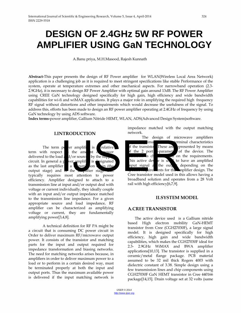
Fig(1): CREE CGH27030F Transistor
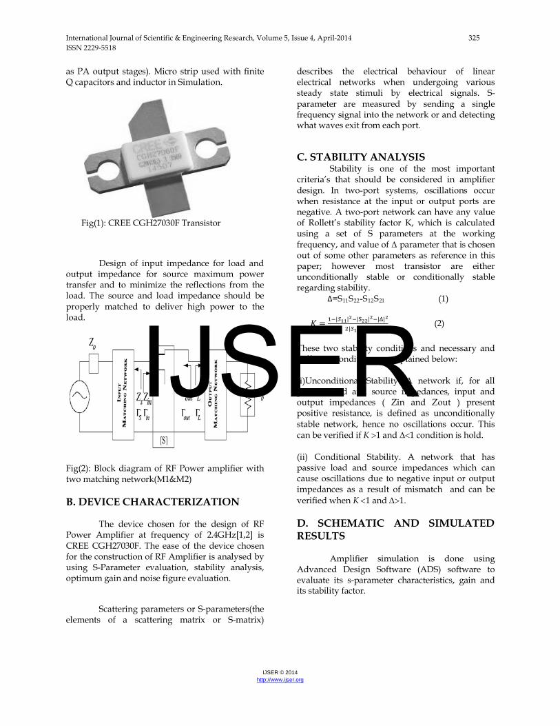
Design of input impedance for load and output impedance for source maximum power transfer and to minimize the reflections from the load. The source and load impedance should be properly matched to deliver high power to the load.
Fig(2): Block diagram of RF Power amplifier with two matching network(M1&M2) B. DEVICE CHARACTERIZATION
The device chosen for the design of RF Power Amplifier at frequency of 2.4GHz[1,2] is CREE CGH27030F. The ease of the device chosen for the construction of RF Amplifier is analysed by using S-Parameter evaluation, stability analysis, optimum gain and noise figure evaluation.
Scattering parameters or S-parameters(the elements of a scattering matrix or S-matrix)
describes the electrical behaviour of linear electrical networks when undergoing various steady state stimuli by electrical signals. S-parameter are measured by sending a single frequency signal into the network or and detecting what waves exit from each port.
C. STABILITY ANALYSIS Stability is one of the most important criteria’s that should be considered in amplifier design. In two-port systems, oscillations occur when resistance at the input or output ports are negative. A two-port network can have any value of Rollett’s stability factor K, which is calculated using a set of S parameters at the working frequency, and value of Δ parameter that is chosen out of some other parameters as reference in this paper; however most transistor are either unconditionally stable or conditionally stable regarding stability. Δ=S11S22-S12S21 (1)
𝐾 = 1−|𝑆11|2−|S22|2−|Δ|2
2|𝑆12𝑆21| (2)
These two stability conditions and necessary and sufficient conditions are explained below: (i)Unconditional Stability. A network if, for all passive load and source impedances, input and output impedances ( Zin and Zout ) present positive resistance, is defined as unconditionally stable network, hence no oscillations occur. This can be verified if K >1 and Δ<1 condition is hold. (ii) Conditional Stability. A network that has passive load and source impedances which can cause oscillations due to negative input or output impedances as a result of mismatch and can be verified when K <1 and Δ>1. D. SCHEMATIC AND SIMULATED RESULTS
Amplifier simulation is done using Advanced Design Software (ADS) software to evaluate its s-parameter characteristics, gain and its stability factor.
IJSER
International Journal of Scientific & Engineering Research, Volume 5, Issue 4, April-2014 326 ISSN 2229-5518
IJSER © 2014 http://www.ijser.org
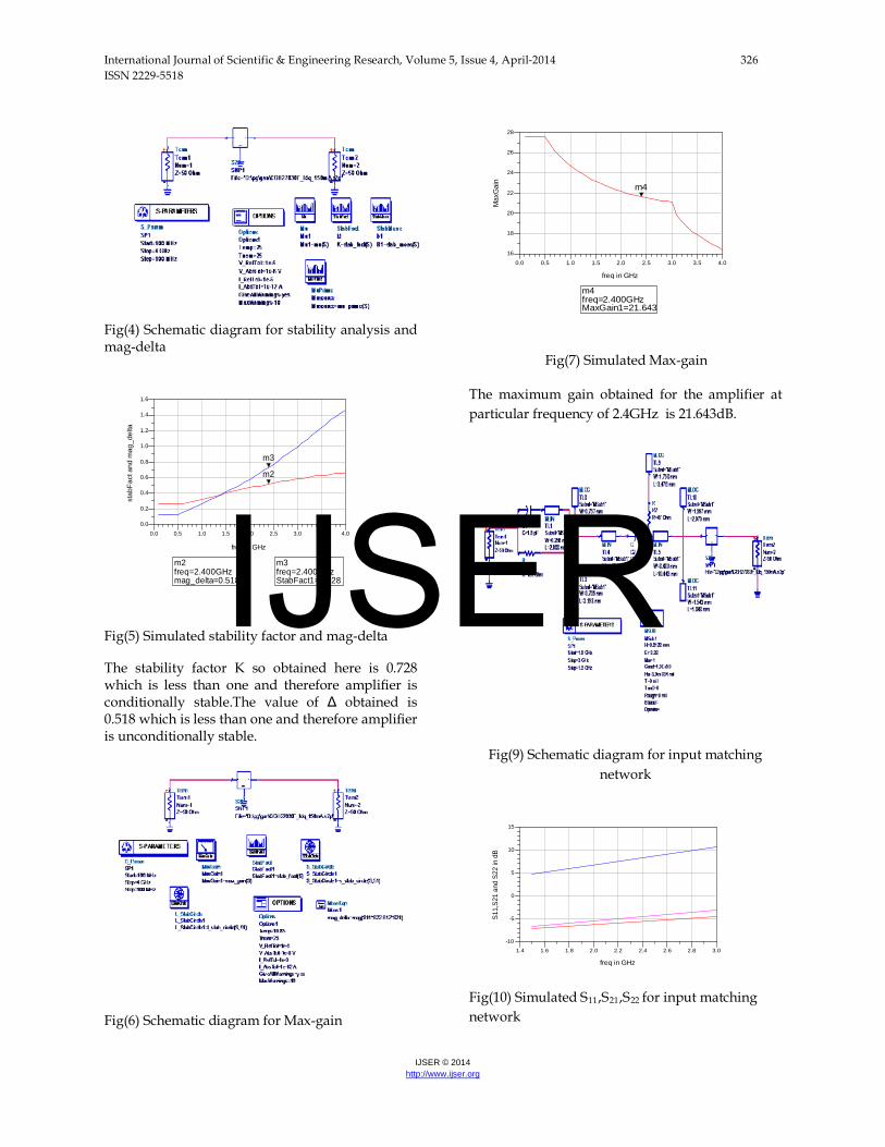
Fig(4) Schematic diagram for stability analysis and mag-delta
Fig(5) Simulated stability factor and mag-delta
The stability factor K so obtained here is 0.728 which is less than one and therefore amplifier is conditionally stable.The value of Δ obtained is 0.518 which is less than one and therefore amplifier is unconditionally stable.
Fig(6) Schematic diagram for Max-gain
Fig(7) Simulated Max-gain
The maximum gain obtained for the amplifier at particular frequency of 2.4GHz is 21.643dB.
Fig(9) Schematic diagram for input matching network
Fig(10) Simulated S11,S21,S22 for input matching network
0.5 1.0 1.5 2.0 2.5 3.0 3.50.0 4.0
0.2
0.4
0.6
0.8
1.0
1.2
1.4
0.0
1.6
freq in GHz
stab
Fact
and
mag
_del
ta
m2
m3
m2freq=mag_delta=0.518
2.400GHzm3freq=StabFact1=0.728
2.400GHz
0.5 1.0 1.5 2.0 2.5 3.0 3.50.0 4.0
18
20
22
24
26
16
28
freq in GHz
Max
Gai
n
m4
m4freq=MaxGain1=21.643
2.400GHz
1.6 1.8 2.0 2.2 2.4 2.6 2.81.4 3.0
-5
0
5
10
-10
15
freq in GHz
S11,
S21
and
S22
in d
B
IJSER
International Journal of Scientific & Engineering Research, Volume 5, Issue 4, April-2014 327 ISSN 2229-5518
IJSER © 2014 http://www.ijser.org
The gain, input and output return loss obtained at particular frequency of 2.4GHz is 8dB,4dB and 6dB.
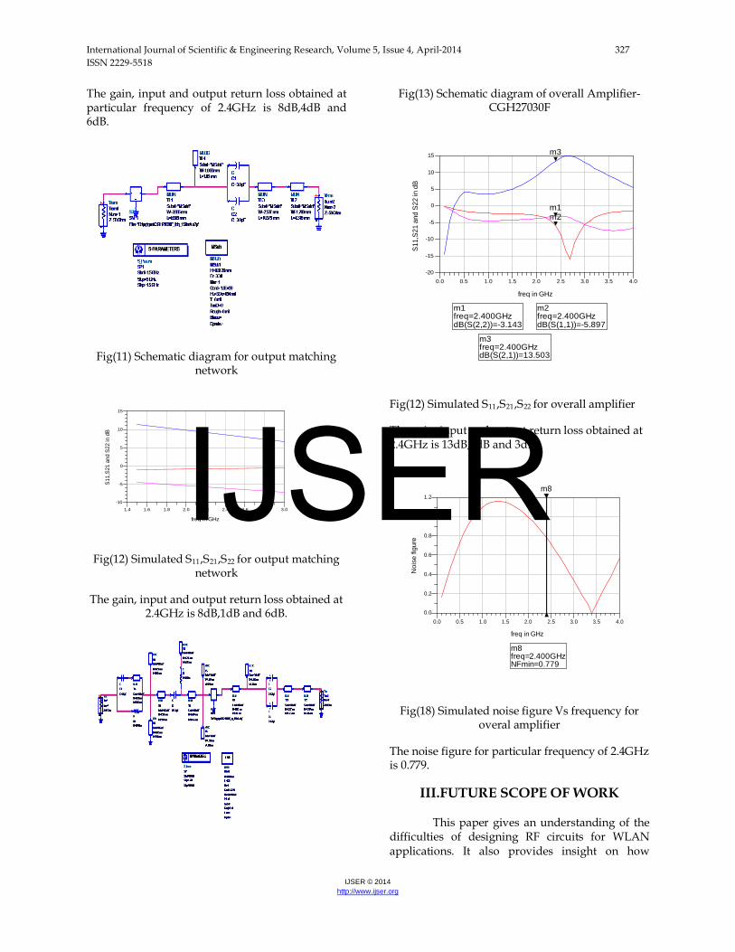
Fig(11) Schematic diagram for output matching network
Fig(12) Simulated S11,S21,S22 for output matching network
The gain, input and output return loss obtained at 2.4GHz is 8dB,1dB and 6dB.
Fig(13) Schematic diagram of overall Amplifier- CGH27030F
Fig(12) Simulated S11,S21,S22 for overall amplifier
The gain, input and output return loss obtained at 2.4GHz is 13dB,5dB and 3dB.
Fig(18) Simulated noise figure Vs frequency for overal amplifier
The noise figure for particular frequency of 2.4GHz is 0.779.
III.FUTURE SCOPE OF WORK
This paper gives an understanding of the difficulties of designing RF circuits for WLAN applications. It also provides insight on how
1.6 1.8 2.0 2.2 2.4 2.6 2.81.4 3.0
-5
0
5
10
-10
15
freq in GHz
S11,
S21
and
S22
in d
B
0.5 1.0 1.5 2.0 2.5 3.0 3.50.0 4.0
-15
-10
-5
0
5
10
-20
15
freq in GHz
S11,
S21
and
S22
in d
B
m2
m3
m1
m2freq=dB(S(1,1))=-5.897
2.400GHz
m3freq=dB(S(2,1))=13.503
2.400GHz
m1freq=dB(S(2,2))=-3.143
2.400GHz
0.5 1.0 1.5 2.0 2.5 3.0 3.50.0 4.0
0.2
0.4
0.6
0.8
1.0
0.0
1.2
freq in GHz
Noi
se fi
gure
m8
m8freq=NFmin=0.779
2.400GHz
IJSER
International Journal of Scientific & Engineering Research, Volume 5, Issue 4, April-2014 328 ISSN 2229-5518
IJSER © 2014 http://www.ijser.org
analysis to be performed before implementing and fabricating the design of RF circuits.
The work to be done is to design of PCB layout for the CREE CGH27030F transistor and has to design the fabrication and testing to obtain the improved efficiency and the measured results are to be analyzed. IV.CONCLUSION
This paper has presented the design of RF Power amplifier operating at 2.4GHz of frequency using CREE CGH27030F(GaN HEMT) transistor with maximum gain of 21.64dB and noise figure obtained as 0.568dB. It is designed mainly for WLAN applications like Bluetooth, Wi-Fi etc REFERENCES
1) Kumar G, Sitaraman S, Sridharan V, Sankaran N, Fuhan L, Kumbhat N, Nair V, Kamgaing T, Juskey F, Sundaram V, and Tummala R 2012. Modeling and design of an ultra-miniaturized WLAN sub-system with chip-last embedded PA and digital dies. IEEE 62nd Electronic Components and Technology Conference, 1015–1022.
2) Yargholi M, and Tarighat A P 2012. Resistive feedback LNA with dual band notch filter for suppressing WLAN signals in UWB receivers. National Conference on Communications, 1–4.
3) Bakkaloglu B and Fontaine P A 2005 Multi-mode, multi-band RF transceiver circuits for mobile terminals in deep-submicron CMOS processes. IEEE Radio Freq. integrated Circuits Symp., 483–486.
4) Nam J, Shin JH, and Kim B. 2005. A handset power amplifier with high efficiency at low level using load modulation technique. IEEE Trans. Microw. Theory Tech., 53, 2639-2644.
5) Raab, FH, Sigmon BE, Myers RG, and Jackson RM. 1998. L-band transmitter using Kahn EER technique. IEEE Trans. Microw. Theory Tech., 46, 2220-2225.
6) Tsai Pi H, Metzger AG, Zampardi PJ, Iwamoto M, and Asbeck PM. 2005. Design of high efficiency current-mode class D amplifier for wireless handsets. IEEE Trans. Microw. Theory Tech., 53,144-151.
7) W. Doherty, “A new high efficiency power amplifier for modulated waves,”
Proc. IRE, vol. 24, no. 9, pp. 1163–1182, Sep. 1936.
8) B. Kim, J. Kim, I. Kim, and J. Cha, “The Doherty power amplifier,” IEEE Microw. Mag., vol. 7, no. 5, pp. 42–50, Oct. 2006.
9) P. Colantonio, F. Giannini, and E. Limiti, High Efficiency RF and Microwave Solid State Power Amplifiers. New York: Wiley, 2009, Microwave and Optical Engineering.
10) [10] S. Cripps, RF Power Amplifiers for Wireless Communications. Norwood,MA: Artech House, 2006.
11) K.-J. Cho, J.-H. Kim, and S. Stapleton, “A highly efficient Doherty feedforward linear power amplifier for W-CDMA base-station applications,” IEEE Trans. Microw. Theory Tech., vol. 53, no. 1, pp. 292–300, Jan. 2005.
12) Y. Yang, J. Cha, B. Shin, and B. Kim, “A fully matched N-way Doherty amplifier with optimized linearity,” IEEE Trans. Microw. Theory Tech., vol. 51, no. 3, pp. 986–993, Mar. 2003.
13) J. Fang, R. Quaglia, J. Rubio, V. Camarchia, M. Pirola, S. Guerrieri, and G. Ghione, “Design and baseband predistortion of a 43.5 dBm GaN Doherty amplifier for 3.5 GHz WiMAX applications,” in Proc. Eur. Microw. Integr. Circuits Conf., Oct. 2011, pp. 256–259.
14) J. Qureshi, N. Li, W. Neo, F. van Rijs, I. Blednov, and L. de Vreede, “A wideband 20 W LMOS Doherty power amplifier,” in IEEE MTT-S Int. Microw. Symp. Dig., May 2010, pp. 1504–1507.
15) K. Bathich, A. Markos, and G. Boeck, “A wideband GaN Doherty amplifier with 35% fractional bandwidth,” in Proc. Eur. Microw. Conf., Sep. 2010, pp. 1006–1009.
IJSER

International Journal of Scientific & Engineering Research, Volume 5, Issue 4, April-2014 329 ISSN 2229-5518
IJSER © 2014 http://www.ijser.org
IJSER