design of 100-900 ghz algaas/gaas planar … of 100-900 ghz algaas/gaas planar heterostructure...
TRANSCRIPT

Design of 100-900 GHz AlGaAs/GaAs PlanarHeterostructure Barrier Varactor Frequency Triplers
1Jan Stake, 'Lars Dillner, 2Stephen H. Jones, 'Chris Mann, and 'Erik Kollberg'Microwave Electronics Laboratory, Chalmers University of Technology, SE412 96 Goteborg,
2University of Virginia, Charlottesville, VA 22903, USA3Rutherford Appleton Laboratory, Chilton, Oxon, UK
Email: [email protected]
Abstract—In this paper we offer a simple setof accurate frequency-domain designequations that can be used to calculateoptimal embedding impedances and triplingefficiency. These equations can be used for awide range of device and circuit parameters.The effects of parasitic resistance andoperating temperature on deviceperformance, and how these parameters varywith device design are exploredComparisons to experiment are made forplanar HBVs demonstrating at least 3%efficiency at 78 GHz input frequency and 50mW of input power.
Index Terms—HBV, varactor frequencytripler.
I. INTRODUCTION
The Heterostructure Barrier Varactor (HBV)diode [1, 2] is ideally suited for frequencytripling in the millimeter wave and sub-millimeter wave regime. The symmetriccapacitance-voltage characteristic of the HBVallows for tripler design without requiringsecond-harmonic idler circuits or DC bias. Inprinciple, this should make HBV triplers easierto design and implement, however, thecomplex device structure and device physicscan make the overall tripler design processmore difficult. In particular, the design andfabrication of the devices are more difficultthan Schottky diode structures used in similarapplications. Subsequently, the output powerand efficiency from Schottky diode varactormultipliers are still somewhat superior to 1-1BV
multipliers [3-5]. In this paper we describe thebasic design concepts, equations, andparameters related to GaAs-AlGaAs-GaAsplanar HBVs.
II. HBV MULTIPLIER ANALYSIS
A. Intrinsic device modelA generic layer structure of an HBV is
shown in table i. For N epitaydally stackedbarriers, the layer sequence 2-5 is repeated Ntimes. The intrinsic part of the HBV consistsof layer 2-6, where a high band-gap material(layer 4) prevents electron transport throughthe structure and the diode capacitance ismodulated due to depletion of carriers in layers2 and 6.
TABLE I: HBV GENERIC LAYER STRUCTURE
Layer ThicknessNo. [A]7 Contact - 30006 Depletion 1- 30005 Spacer s'-504 Barrier b - 2003 Spacer s 502 Depletion 1- 30001 Buffer0 Substrate
In our analysis, we use a two element modelfor the intrinsic part of the HBV: a non-lineardifferential elastance, S(V) = dV/d0 = 1/C00,in series with a non-linear parasitic resistance,R(10. Varactor mode of operation for HBVs is
Doping level[cm'i n.Nd 1017UndopedUndopedUndopedNd 1017
n
n- or SI
359
(4)0R(v(t)) ,S(v(t))
si)KNb 2s w= -xuaa [m2 /9.et, e d d
S(0= S' S'd (t)depletion)
S; (1) 0 N
( Eb),E0)
[1/F]
(3)I(Eh ) = A -aT2Sinh (5)
respectively. The maximum differentialelastance is determined by the maximalextension of the depletion region, wn., as:
preferred and therefore large conductioncurrents should be reduced as much asposssible for optimal performance.
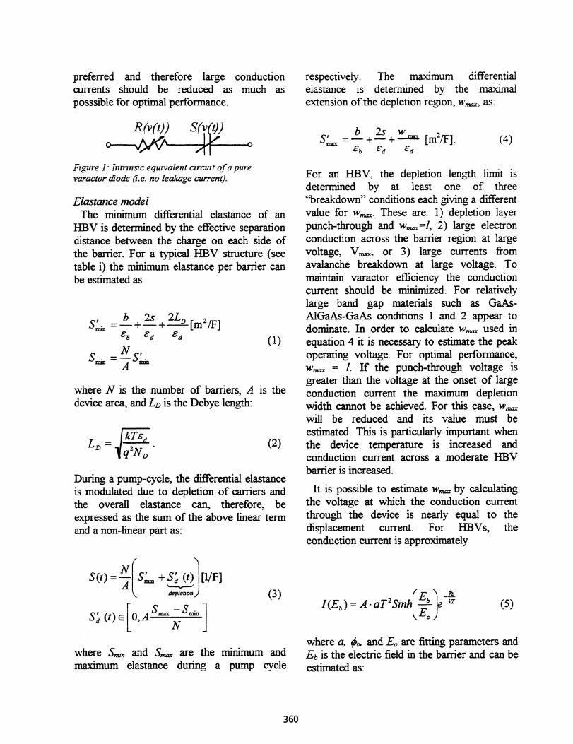
Figure 1: Intrinsic equivalent circuit of a purevaractor diode (i.e. no leakage current).
Elastance modelThe minimum differential elastance of an
HBV is determined by the effective separationdistance between the charge on each side ofthe barrier. For a typical HBV structure (seetable i) the minimum elastance per barrier canbe estimated as
b 2s 21,= — + - ----24111 2 51
eb ed ed
– — S r -A
where N is the number of barriers, A is thedevice area, and Lip is the Debye length:
r) kTeiiq 2ND
During a pump-cycle, the differential elastanceis modulated due to depletion of carriers andthe overall elastance can, therefore, beexpressed as the sum of the above linear termand a non-linear part as:
For an HBV, the depletion length limit isdetermined by at least one of three"breakdown" conditions each giving a differentvalue for w„.. These are: 1) depletion layerpunch-through and wn.=/, 2) large electronconduction across the bather region at largevoltage, Vmax, or 3) large currents fromavalanche breakdown at large voltage. Tomaintain varactor efficiency the conductioncurrent should be minimized. For relativelylarge band gap materials such as GaAs-AlGaAs-GaAs conditions 1 and 2 appear todominate. In order to calculate wn. used inequation 4 it is necessary to estimate the peakoperating voltage. For optimal performance,Wfl ff = I. If the punch-through voltage isgreater than the voltage at the onset of largeconduction current the maximum depletionwidth cannot be achieved. For this case, wn.will be reduced and its value must beestimated. This is particularly important whenthe device temperature is increased andconduction current across a moderate 1113Vbarrier is increased.
It is possible to estimate wn. by calculatingthe voltage at which the conduction currentthrough the device is nearly equal to thedisplacement current. For HBVs, theconduction current is approximately
(1)
(2)
where S,„,„ and Sn. are the minimum andmaximum elastance during a pump cycle
where a, 4, and Eo are fitting parameters andEb is the electric field in the barrier and can beestimated as:
360

di (V ,T)
dV« (D Cp
V=Vrl
(7)
which in combination with (8) gives:
Eb qN d
be +
2
2se
beb
(6)de:V.„,
1( Ill+2e
NqN d (be d +2seb)2
J
Taking the derivative of equation (5) (deviceconductance) and given:
R(t) = + - se•C'd( t))). (10)
B. The frequency tripler circuitThe time-dependent voltage, v(t), across the
diode terminals in figure 1 can with the aboveproposed HBV model (3,10) be written as:
v(t) = - (i + NPdS4 S'd(t)i(t).( 1 1)
+5S(t)i(t)di
For strong conduction, one can solve for Vmaxand wmar where conduction is dominant.
Intrinsic Series ResistanceThe parasitic series resistance is the sum of
the resistance of undepleted active layers, thespreading resistance, and the ohmic contactresistance. However, only the resistance ofundepleted layers contributes to the intrinsicvaractor model shown in figure 1. All extrinsicimpedances can be regarded as a part of theembedding circuit, see figure 2. If thedepletion layer, No. 2,6 in Table I, ishomogeneously doped and an abrupt spacecharge is assumed, the resistance of undepletedlayers can be expressed as a function of thelength of the depleted region, w, as
R(t) = +NO - w (0))(8)
w (t) [0,1]
where 1 is the length of the depletion layer andPd is the corresponding resistivity. Forsimplicity, the extension of the depletionregion, w(t), is assumed to be proportional tothe elastance as
w(t) = eS(t) (9)
HBV Diod
Intrinsic
Part
z,
Figure 2: Schematic view of an HBV tripler circuit.
Since we are interested in the periodicsteady-state solution of the above circuitequation (11), we represent the voltage-, thecurrent- and the elastance-waveforms in thefrequency domain and the time-domainequation takes the following form for the kthharmonic [7,11]:
V k — (1 + NYk +— I_ )22 NS' -
jk cop(12)
Ni
1A 47, PA!) k- I
+—11‘ Zi P
I= --co
The two first terms are linear but the last termaccounts for the complex movement of thedepletion edge. The current and the elastance
P.3
361

Rc.1
harmonics can be found by imposingembedding circuit conditions
= Viwurcec, k + p,k) k (13)
where Zc,k = Rc,k tge,k is the embeddingcircuit impedance and ZAk = Rpjc -
r-iXp,k is the
extrinsic parasitic impedance, see figure 2.Furthermore, define the complex modulationratio as 1Vric = SV(S
"max-S
"min) and a general
form of the large-signal device impedance, Zd.k,
within our varactor circuit model can bewritten as:
= +N)A A jka
(14)
1 1 c°
j—ka) Pd6d EirAfei,k-1k
Optimal embedding impedancesThe summation over all current and elastance
harmonics in (14) is a complex value whichdepends slightly on circuit conditions (13) andon physical details of the HBV itselfHowever, for maximum conversion efficiencywhen all available pump-power is absorbedand the third harmonic power delivered to theload is maximized; we assume that thiscomplex summation is independent on externalconditions and HBV layer structures.Consequently, the optimal embeddingimpedances, 4,„ close to any operating pointcan be expressed as
RP*L
A—Am--sLink—Lwp—P
N_x .4_j A a)
+—N
(S' —S'.A max mm
R R +241
+—(S' —S'III2X. Mill
3co
p Pd6dC3)
N S"„,„,P,3 A 30)
P
(B,
±—A (Sima( — St.)
3(0 —PdeeD3)
p
where Am Bm C„, and D„ are fittingcoefficients. If these parameters are extractedfor realistic operating conditions and withaccurate large-signal device simulator, theabove optimal embedding impedances can becalculated for a wide range of device andcircuit parameters.
Dynamic cut-off frequencyThe dynamic cut-off frequency of a pure
varactor device (i.e. no leakage current) isdefined as:
f= — Smin
22r..4 *(16)
With the proposed intrinsic varactor model inSection Ha, define the series resistance as thesum of the maximal value of the intrinsicresistance (8) and the real part of the extrinsicparasitic impedance at the fundamentalharmonic. If the equations for maximal andminimal elastance and the series resistance are
PdedD(pp
(15)
362

PAVA
w max — 2LD, (17)
p,1 + pd10 + N))
fc. = N27red
1 + a
inserted in (16), the dynamic cut-off frequencyfor an HBV can finally be calculated as:
As shown above, it is very important to reducethe parasitic resistance as much as possiblerelative to the intrinsic device resistance. Also,Wm= should be large relative to Ld to insuresignificant capacitance modulation and tripling.As described above, to optimize fc theconduction current should minimized andwmar=1-
Pump power and conversion efficiencyThe conversion efficiency is defined as the
power delivered to the load at the thirdharmonic divided by the available input powerand for a pure varactor multiplier, theefficiency is determined by the ratio of thepump-frequency and the dynamic cut-offfrequency [6, 7]. A quick and fast estimationof the maximum conversion efficiency can beachieved from the following empiricalexpression
(18)
where a and )6 are extracted from detailedlarge-signal simulations for a wide range ofdevices and circuit conditions, see table ii. Formaximum possible efficiency ef, should beincreased to its maximal value as described inequation 17.
Finally, it is necessary to estimate the inputpower needed to modulate the elastance of anREV from Smin to Sm. The pump-power canbe estimated as
111 2 R c. , 2
1 2 III8R, 21Z411
R1
2 2II .1
— Z:
where 7 is also a fitting coefficient, see table ii.Equation 19 insures that reasonable deviceparameters and required input powers aredesigned for a particular application.
RESULTS AND DISCUSSION
A. Parameter extractionAll the coefficients were extracted by
analyzing two four-barrier HBVs with anintegrated Drift-Diffusion Harmonic Balance(DDHB) simulator [8, 9]. The pump frequencywas 90 GHz and the device area 66 iim2. Allsimulations were performed by assuming ahomogenous temperature of T = 300 K acrossthe active device region. A field-independent(low field) electron mobility of 4375 cm2Ns inthe GaAs region and a calculated extrinsicparasitic series resistance of R .1 = 4.9 ohmwere used. Intrinsic losses, e.g. ohmic losses inlayers (No. 2,6), are fully taken into accountby the DDHB simulator. The conversionefficiency was maximized by tuning theembedding impedances at the first and thethird harmonic respectively. Finally,coefficients for the design equations(15,18,19) were extracted, see table ii. Thesecoefficients allow the optimal embeddingimpedances and efficiency to be easilycalculated.
TABLE II: HBV DESIGN COEFFICIENTS
Extraction conditions: f4-0.05 A i = 0.047 .8 = 0.33 C1 = -0.17 D1 = -2.5A3 = O.24 B3 = 0.66 C3 = -1.3 D3= 4.9a= 200 fl = 1.4 y = 0.7
(19)
363

Comparison to experimental resultsDevice structure and measured performance
The epitaxial layer structure in table iii hasbeen fabricated into a planar HBVconfiguration, see figure 4.
TABLE III: UVA-NRL-1174
Layer Material Doping Thickness[cm] IA]
9 InAs 5x10'8 1008 Ini-oDGaAs 5x10'
84007 GaAs 5x10'8 30006 GaAs 8x 10
1625005x4 GaAs Undoped 354x4 A10,7GaAs Undoped 2003x4 GaAs Undoped 352x4 GaAs 8x10'6 2500
GaAs 5x10¹⁸ 40000GaAs SI
An 1113V device with an anode area of 89 gm2was mounted and tested in a tripler waveguideblock ('RAL DB2a). A flange-to-flange peakefficiency of 3.1 % was achieved at an outputfrequency of 234 GHz. The maximal outputpower was 3.6 mW, see figure 3. Theestimated loss at the input- and output circuitare approximately I dB and 2 dB respectively.
heating must be taken into account. This hasbeen described in section HA. For a 8 umdiameter device and by assumin g a point heat-source in the middle of the active region, Jones[10] has estimated the thermal resistancethrough the finger and the GaAs substrate to
= 2 K/mW for this device geometry.Furthermore, if we assume that the thermalresistance is inversely proportional to theanode diameter and an input circuit loss of 1dB, the device temperature can be as high as400 K for the 10 pm (891..um2) HBV used andan available pump power of 80 mW.
Figure 4: Planar HBVs (UVA-NRL-1174-17).
The extrinsic parasitic series resistanceconsists of the ohmic contact resistance andthe spreading resistance in the n island thatconnects the two diodes. By using standardexpressions for these losses, we canapproximate the temperature dependentparasitic series resistance as
Figure 3: Measured output power and efficiency at anoutput _frequency of 234 GHz.
Estimated thermal and parasitic resistanceIn order to explain the lower than expected
efficiency shown in figure 3, the effect of self-
Z = 4,3
200 ( 20 100) T (20)4 +„LT A ) 298
where A is the anode area in gm2 . The firstterm represents the contact resistance and thesecond term estimates the spreading resistancein the n' island.
Conversion efficiencyThe negative effect of heating on the dynamic
cut-off frequency (17) results from thetemperature dependence of the seriesresistance (20) and the Debye-length (2), aswell as the reduction in maximal depletionlength, as the temperature increases.
364

1---- CO Cp MIX (21)
V=Vrt( 10
4 6 8Vdtege lvdti
0,4C)
• 0,3•-=•,
-0,2
-; 3
j.0,1
-1010 12 14
10 2
1000
T=24*C
Figure 5: Measured C-V (R7) and I-V (RT-186°C)characteristics of the UVA-NRL-1174 HBV material.
The conversion efficiency increases with pumppower as long as the conduction currentthrough the barrier is negligible compared tothe displacement current. The measured I-Vcharacteristic versus temperature and C-Vcharacteristic for the UVA-NRL-1174 deviceare shown in Figure 5. The parameters: a=170 Al(m2K
2), -0 = 4.2x10⁶ V/rn, and =0.17 eV in (5) provides an excellent fit withmeasured I-V characteristic at differenttemperatures. As a guideline, to ensurevaractor mode of operation, the maximumvoltage, V,„ can be estimated versustemperature as:
dI(V,T) dV
The value of 1/10 can be adjusted significantlyand only have a minor effect on the overallvalue of the efficiency.
Using the analysis outline in HA. wmax wascalculated for temperatures ranging from 250-500 K. Then, the predicted efficiency over thisrange was calculated using equations (17,18)with the coefficients in Table II. The resultsare shown in Figure 6 (including 3 dB ofcircuit loss). The experimental results areshown. As seen, the efficiency is reduced athigher temperatures as the conduction currentincreases and wmax < 1. Also, if the parasitic
resistance is reduced the entire curve will shiftup. For Figure 6 the parasitic resistance isapproximately 12 ohms and calculated usingequation 20.
10%lotret trough krnted
8% ouru tegsncy: 234 GutzDew tree: 89 ;sr
Cortkicbcn osrert tp.t omit losses: 1 de6% .rtrrited CU= crust losses: 2 dB
4%
2%thiesared peak-erkoercy 77mW
(R - 1.6 IGtriN)0%
250 300 350 400 450 500Term:entre pq
Figure 6: Maximal efficiency versus devicetemperature.
Finally, with the design-coefficients in tableand equations (1-2,4,15,20) the optimalembedding impedances for a devicetemperature of 400 K can be estimated: Z . 1 =21 j97 and Z,3 = 27 ± j36.
IV. CONCLUSIONS AND SUMMARY
We have described a complete model thatcan be used to predict the optimal embeddingimpedances and efficiency for BBVs. Theimportant effects of self heating and the needto minimize parasitic resistance have beendescribed. Comparisons to experimentalresults are favorable. Based one the analysisdescribed here a new set of HBVs have beendesigned and will be tested in the near future.
V. ACKNOWLEDGMENT
Jan Stake was supported during this work bythe SSF High Speed Electronics program. Thework was also partly sponsored by grants fromLM Ericsson and the Royal Swedish Academyof Sciences. Thanks are due to William L.Bishop, Art Lichtenberger, Benjamin Sarpong,Steven Marazita, and Tom Crowe of theSemiconductor Device Laboratory at the
365

Theoretical Investigation of theHeterostructure Bather Varactor." in Schoolof Electrical Engineering. Charlottesville:University of Virginia, 1996.
University of Virginia for their support duringdevice fabrication.
REFERENCES
[11 E. L. Kollberg and A. Rydberg, "Quantum-barrier-varactor diode for high efficiencymillimeter-wave multipliers," Electron. Lett.,vol. 25, pp. 1696-1697, 1989.
[2] A. Rydberg, H. GrOnqvist, and E. L. KoLlberg."Millimeter- and Submillimeter-WaveMultipliers Using Quantum-Barrier-Varactor(QBV) Diodes," IEEE Trans. ElectronDevices, vol. 11, pp. 373-375. 1990.
[3] N. R Erickson, "High EfficiencySubmillimeter Frequency Multipliers,"presented at IEEE MTT-S, Dallas, 1990.
[4] N. R. Erickson, "A High Efficiency FrequencyTripler for 230 GHz," presented at 12thEuropean Microwave Cont Helsinki, 1982.
[5] J. Thornton, C. M. Mann, and P. d. Maagt,"A High Power 270 GHz Frequency TriplerFeaturing a Schottky Diode Parallel Pair,"presented at IEEE-MTT Int. MicrowaveSymp. Digest, Denver, USA, 1997.
[6] L. Dinner, J. Stake, and E. L. Kollberg,"Analysis of Symmetric Varactor FrequencyMultipliers," Microwave Opt. Technol. Lett.,vol. 15, pp. 26-29, 1997.
P. Penfield and R. P. Rafuse, VaractorApplications. Cambridge: M.I.T. Press, 1962.
J. R. Jones, G. B. Tait, S. H. Jones, and S. D.Katzer, "DC and Large-Signal Time-Dependent Electron Transport inHeterostructure Devices: An Investigation ofthe Heterostructure Barrier Varactor," IEEETrans. Electron Devices, vol. 42, pp. 1393-1403, 1995.
[9] J. Stake, S. H. Jones, J. R. Jones, and L.Dinner, "Analysis of Carrier Transport in aHeterostructure Barrier Varactor DiodeTripler," presented at 1997 InternationalSemiconductor Device Research Symposium,Charlottesville, 1997.
[10] J. R. Jones, "CAD of Millimeter WaveFrequency Multipliers: An Experimental and
[11] R. E. Lipsey, S. H. Jones. and T. W. Crowe."Accurate Circuit and Device Equations forDesigning 50-600 GHz GaAs Schottky DiodeVaractor Frequency Doublers", presented atEight International Symposium on SpaceTerahertz Technology. Boston, 1997.
366