design, modeling, testing, and spice parameter extraction...
TRANSCRIPT
DESIGN, MODELING, TESTING, AND SPICE PARAMETER EXTRACTION OF DIMOS TRANSISTOR IN 4H-SILICON CARBIDE
MD HASANUZZAMAN1, SYED K. ISLAM1,2, LEON M. TOLBERT1,2, BURAK OZPINECI2
1Department of Electrical and Computer Engineering The University of Tennessee, Knoxville, TN 37996-2100
2Oak Ridge National Laboratory, National Transportation
Research Center, Oak Ridge, TN 37831-6472
Received (31 January 2005) Accepted (26 May 2005)
In this paper, an analytical model for a vertical double implanted metal-oxide semiconductor (DIMOS) transistor structure in 4H-Silicon Carbide (SiC) is presented. Simulation for transport characteristics of the SiC MOSFET with the exact device geometry is carried out using the commercial device simulator MEDICI. A rigorous experimental testing and characterization is done on a 4H-SiC DIMOS transistor test device. SPICE parameters are extracted from the measurements, and a SPICE model for the DIMOS transistor has been developed. The presented work is a part of team efforts of material, device, and power electronics researchers at the University of Tennessee and Oak Ridge National Laboratory.
1. Introduction Silicon carbide (SiC), a wide bandgap material, shows a tremendous potential for high temperature electronics applications and offers significant advantages for power switching devices. It has a high electric breakdown field (3.5x10⁶ V/cm), a high electron saturated drift velocity (2x107 cm/sec), a high melting point (2830 oC), and a high thermal conductivity (4.9 W/cm-°K) that give it a great potential for high-temperature and high-power device applications.1-4 Among the wide bandgap materials, SiC is the most advanced one in the context of better quality material growth, defect-free dielectric formation, implantation doping, contacts via metallization, and other process steps. Dc-dc converters and ac drives are extensively used in power electronics, power systems, traction drives, and hybrid electric vehicle (HEV) applications, where diodes and MOSFETs are used as switching devices. These devices have to carry large currents

during the ‘on’ state and have to sustain large blocking voltages during the ‘off’ state. The performance of the silicon- (Si)-based switches is approaching the theoretical limits in high power applications due to its intrinsic material properties. SiC is an alternate material that can be used to overcome the limitations of the Si-based switching devices. Although there are no commercially available power MOSFETs in SiC material, Cree has demonstrated various switching devices in SiC.5 A group from Purdue University proposed a DIMOS in 6H-SiC with a breakdown voltage of 760V.6 Presently, most of the research effort in SiC is on the design and fabrication of power MOSFETs. However, theoretical models of these prototypes have to be developed to study the behavior of these devices and fine-tune their characteristics. Since SiC MOSFETs are still in their infancy, there is a good opportunity now to study and model these devices so that the model can be verified using actual SiC MOSFET test devices. A good reliable device model is essential for the evaluation of the device behavior and its characteristics. A precise model can predict the device behavior more accurately and thus, the design requirements can be implemented with tight tolerances. This paper provides a brief overview of the state-of-the-art research in the area of silicon carbide device modeling. A thorough and detailed analysis of a SiC power MOSFET, modeling, simulation, testing, and characterization of a test device, and the extraction of parameters for a SPICE model are presented. An application specific optimum SiC power MOSFET is being developed for hybrid electric vehicle applications.7 The system level benefits of SiC power electronics for hybrid electric vehicle (HEV) applications was also studied.8 Considering the SiC
n+
n+
n+
p-body p-body
Oxide
S SG
D
Region A
Region B
Region C
α
Ls
LpL
Wd
Wj
Wt
Figure 1. DIMOS structure for modeling. Labels describe the different regions and
dimensions of the vertical structure

material processing limitations and feedback from the system level application group, an application specific SiC power MOSFET structure has been proposed. 2. Modeling of Vertical DIMOS Device 2.1 Model: An analytical model for a DIMOS field effect transistor is developed using SiC material. The model is developed based on the methodology for a vertical double diffusion MOS model.9-12. The proposed DIMOS model incorporates the effect of SiC device behavior. Figure 1 shows the details of the device structure identifying the different regions of operation. The model is developed from regional analyses of carrier transport in the channel and the drift regions. The active channel exists below the oxide layer and within the p-bodies. The current/voltage characteristic in the triode region is given by Eq. 1,
[ ] [ ]chdooxTGSoxchchsatn
nch VCCVVCV
VLvLW
I )()(2)2/(12
+−−+
=µ
µ (1)
where W is the channel width, L is the channel length, Vch is the channel voltage, VT is the threshold voltage, VGS is the gate voltage, Cox is the oxide capacitance, Cdo is the body depletion capacitance, µn is the electron mobility, and vsat is the electron saturation velocity. The drift region is divided into three parts:
an accumulation region-A, a drift region-B with a varying cross-section area, and a drift region-C with constant cross-section. The corresponding voltages to these regions are VA, VB, and VC for region A, B, and C, respectively, and they are given by the following equations
∫+
−
+==
dj WW
CDnds
djDyA EIqNLW
WWIdyEV
0 /)()(
µ (2)
−
−+=
CDnsd
CDPsnd
nd
DB EILWqN
EILLWqNWqN
IV
//)2(
logcot µ
µαµ
(3)
( )cDPSnd
PdjtDC EILLWqN
LWWWIV
−+
−−−=
)2(tan
µα (4)
where Wj is the depth of n+ contact region, Wd is the depth of depletion region, Wt is the total thickness of epilayer, Ls is the length of accumulation region, and Lp is the length of p-body. Total drift region voltage is Vdrift = VA + VB + VC ,
and the voltage across the drain and the source is VDS = Vdrift + Vch. The voltages and the currents of the above mentioned two sets of equations for the drift region and the channel region are implicitly related. The drain current, ID is equal to the total channel current Ich, which sets a relationship between the two sets of equations. An iterative solver was
n+
n+
n+
p-body p-bodyChannel
Oxide
S SG
D
4H-SiC n- driftregion
Rn+
RARCH
RJ
RD
RS
Rn+RCH
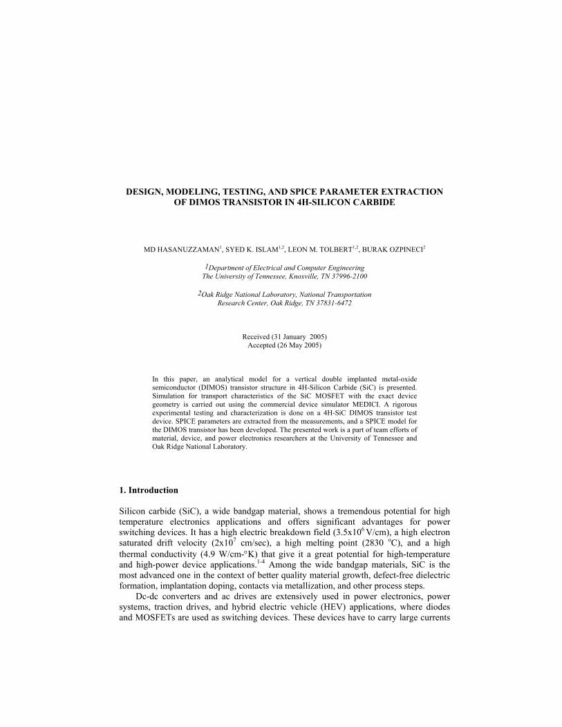
Figure 2. Schematic cross section of vertical DIMOS structure used in MEDICI device simulator.
developed to evaluate the voltages and the currents. 4H-SiC material parameters were used to evaluate the model. 2.2 Device Structure: A vertical double implanted MOSFET (DIMOS) in 4H-SiC is considered for verification of the analytical model developed earlier. The cross-sectional view of the proposed DIMOS structure is shown in Figure 2. A summary of the device structure and doping levels is shown in Table I. The proposed device structure and the device dimensions are selected in such a way that a practical device can be built on the basis of currently available SiC technology. Since the diffusion process in SiC is negligible, ion implantation is the only way to form the p-
Table I. Device Dimensions for the Proposed 4H-SiC DIMOS
Doping Device dimensions
Region Doping level Impurity
Channel width 400 µm n-drift 4x1015cm-3 Nitrogen Channel length 1 µm p-bodies 4x1017cm-3 Aluminum
Oxide thickness 500 Å n+ region 1.5x1020cm-3 Nitrogen
p-bodies separation 20 µm
Epilayer thickness 25 µm
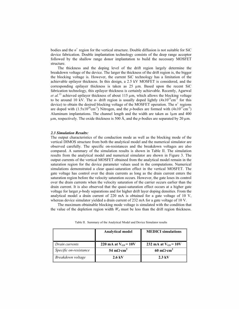
bodies and the n+ region for the vertical structure. Double diffusion is not suitable for SiC device fabrication. Double implantation technology consists of the deep range acceptor followed by the shallow range donor implantation to build the necessary MOSFET structure. The thickness and the doping level of the drift region largely determine the breakdown voltage of the device. The larger the thickness of the drift region is, the bigger the blocking voltage is. However, the current SiC technology has a limitation of the achievable epilayer thickness. In this design, a 2.5 kV MOSFET is considered, and the corresponding epilayer thickness is taken as 25 µm. Based upon the recent SiC fabrication technology, this epilayer thickness is certainly achievable. Recently, Agarwal et al.13 achieved epilayer thickness of about 115 µm, which allows the blocking voltage to be around 10 kV. The n- drift region is usually doped lightly (4x1015cm-3 for this device) to obtain the desired blocking voltage of the MOSFET operation. The n+ regions are doped with (1.5x1020cm-3) Nitrogen, and the p-bodies are formed with (4x1017cm-3) Aluminum implantations. The channel length and the width are taken as 1µm and 400 µm, respectively. The oxide thickness is 500 Å, and the p-bodies are separated by 20 µm. 2.3 Simulation Results: The output characteristics of the conduction mode as well as the blocking mode of the vertical DIMOS structure from both the analytical model and the numerical simulator are observed carefully. The specific on-resistances and the breakdown voltages are also compared. A summary of the simulation results is shown in Table II. The simulation results from the analytical model and numerical simulator are shown in Figure 3. The output currents of the vertical MOSFET obtained from the analytical model remain in the saturation region for the device parameter values used in the computations. Numerical simulations demonstrated a clear quasi-saturation effect in the vertical MOSFET. The gate voltage has control over the drain currents as long as the drain current enters the saturation region before the velocity saturation occurs. However, the gate loses its control over the drain currents when the velocity saturation of the carrier occurs earlier than the drain current. It is also observed that the quasi-saturation effect occurs at a higher gate voltage for larger p-body separations and for higher drift layer doping densities. From the analytical model a drain current of 220 mA is obtained for a gate voltage of 10 V, whereas device simulator yielded a drain current of 232 mA for a gate voltage of 10 V. The maximum obtainable blocking mode voltage is simulated with the condition that the value of the depletion region width Wd must be less than the drift region thickness.
Table II. Summary of the Analytical Model and Device Simulator results
Analytical model MEDICI simulations
Drain currents 220 mA at VGS = 10V 232 mA at VGS = 10V Specific on-resistance 54 mΩ·cm2 60 mΩ·cm2
Breakdown voltage 2.6 kV 2.3 kV

The gate is grounded for the blocking mode operations. The analytical model shows the breakdown voltage of 2.6 kV whereas MEDICI simulation shows 2.3 kV. The doping density and the drift region thickness are calculated for a breakdown voltage of 2.5 kV.
The required doping density is 4.2x1015 cm-3 and the corresponding drift region thickness is 25 µm. Figure 3(c) shows the comparison of the theoretical and the simulated values of the breakdown voltages with the drift layer thickness as a parameter. The simulated values closely follow the theoretical one.
(a) (b)
(c) (d)
Figure 3. Output characteristics of (a) Analytical model, (b) MEDICI simulation, (c) Variation of breakdown voltage with doping density, (d) Variation of specific on-resistance with gate width.
The impact of increasing gate width upon the specific on resistance is shown in Figure 3(d). The channel and the accumulation layer resistances increase with the gate width. On the other hand, the resistance of the drift region decreases because of the increase in the cross sectional area for current flow. The optimum gate width obtained from this design is 20µm. The on-resistances for both cases are calculated from the slope of the tangent drawn at the origin of the output characteristics (Figure 3(a) and Figure 3(b)). The on-resistances are multiplied by the cross-sectional area of 8 ×10⁻⁴cm2 of the drift region between the p-bodies to obtain the specific on-resistances. The calculated

Table III. 4H-SiC DIMOSFET Test Device Specifications
Maximum current rating 2 A Blocking voltage 1.2 kV Threshold voltage 3.2 V On-resistance 1 Ω at VGS = 20V Channel length 1.5 µm
value of the specific on-resistances for the analytical model is 54 mΩ·cm2, and for the numerical simulator is 60 mΩ·cm2. However, the theoretical value of the specific on-resistance is 45 mΩ·cm2.
3. Testing, Characterization, and Parameter Extraction As a part of the current research, a DIMOSFET fabricated in 4H-SiC has been tested and characterized at room temperature and at elevated temperature. The test device was obtained with the collaboration of Cree Research Inc., Raleigh, North Carolina. The specification of the device is given in Table III. Due to the limitation in the testing facilities, only DC or static characterization and switching of an inverter circuit have been carried out. Breakdown voltage test was not carried out due to the limited supply of test devices.
DUT
GPIB
HP 4145B ParameterAnalyzer
Data Acquisition &Control Computer
(a)
DUTGPIB
Data Acquisition &Control Computer Keithley 590 CV
Analyzer
(b)
TestCircuit
TDS 340A DigitalOscilloscope
DC PowerSupply
Signal GeneratorHP33120A
(c)
Figure 4. Test setup for (a) DC characterization, (b) Capacitance measurement, (c) Switching characteristics
(a) (b)
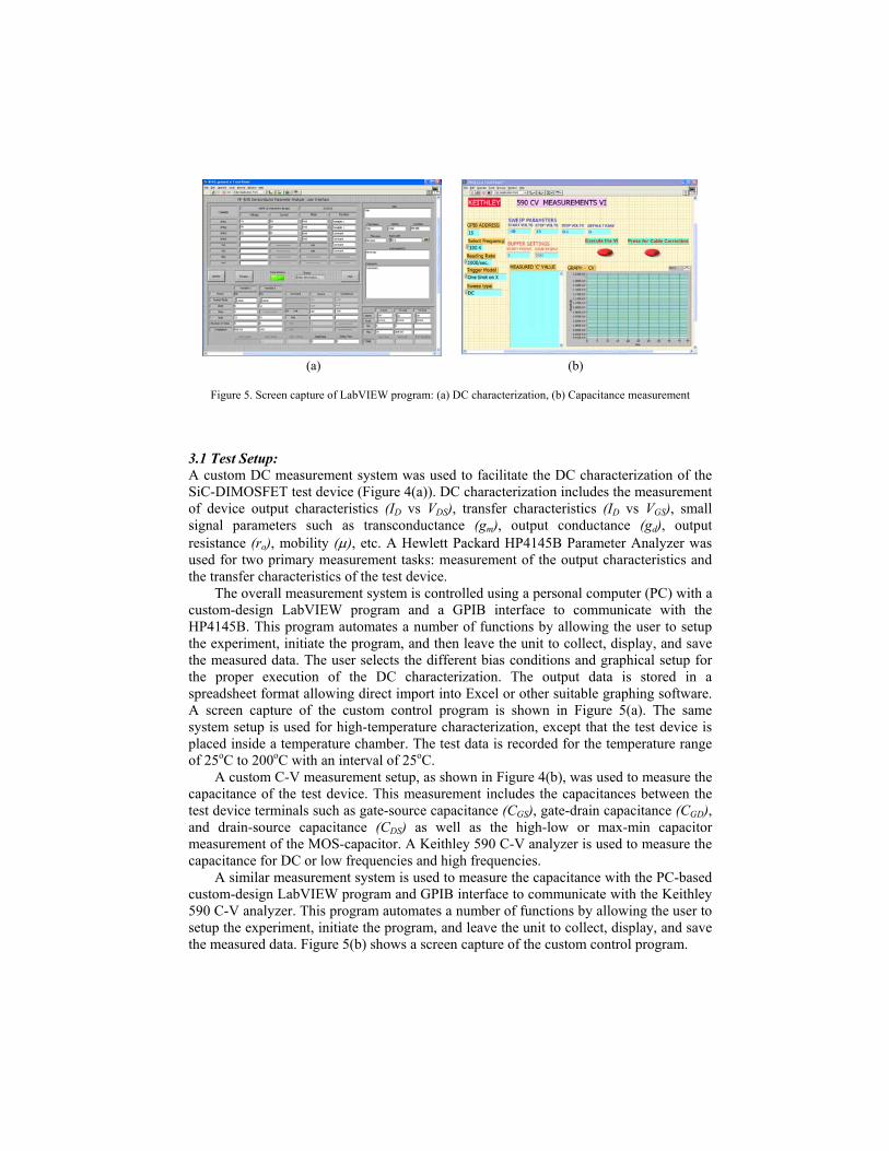
Figure 5. Screen capture of LabVIEW program: (a) DC characterization, (b) Capacitance measurement
3.1 Test Setup: A custom DC measurement system was used to facilitate the DC characterization of the SiC-DIMOSFET test device (Figure 4(a)). DC characterization includes the measurement of device output characteristics (ID vs VDS), transfer characteristics (ID vs VGS), small signal parameters such as transconductance (gm), output conductance (gd), output resistance (ro), mobility (µ), etc. A Hewlett Packard HP4145B Parameter Analyzer was used for two primary measurement tasks: measurement of the output characteristics and the transfer characteristics of the test device. The overall measurement system is controlled using a personal computer (PC) with a custom-design LabVIEW program and a GPIB interface to communicate with the HP4145B. This program automates a number of functions by allowing the user to setup the experiment, initiate the program, and then leave the unit to collect, display, and save the measured data. The user selects the different bias conditions and graphical setup for the proper execution of the DC characterization. The output data is stored in a spreadsheet format allowing direct import into Excel or other suitable graphing software. A screen capture of the custom control program is shown in Figure 5(a). The same system setup is used for high-temperature characterization, except that the test device is placed inside a temperature chamber. The test data is recorded for the temperature range of 25oC to 200oC with an interval of 25oC. A custom C-V measurement setup, as shown in Figure 4(b), was used to measure the capacitance of the test device. This measurement includes the capacitances between the test device terminals such as gate-source capacitance (CGS), gate-drain capacitance (CGD), and drain-source capacitance (CDS) as well as the high-low or max-min capacitor measurement of the MOS-capacitor. A Keithley 590 C-V analyzer is used to measure the capacitance for DC or low frequencies and high frequencies. A similar measurement system is used to measure the capacitance with the PC-based custom-design LabVIEW program and GPIB interface to communicate with the Keithley 590 C-V analyzer. This program automates a number of functions by allowing the user to setup the experiment, initiate the program, and leave the unit to collect, display, and save the measured data. Figure 5(b) shows a screen capture of the custom control program.

0.00
0.01
0.02
0.03
0.04
0.05
0.06
0.07
0 2 4 6 8 10Drain Voltages, VDS (V)
Dra
in C
urre
nts,
I D (A
mp) Vgs=4V
Vgs=5VVgs=6VVgs=7V
Rds-on =14ohm at Vgs=7V
0.00
0.02
0.04
0.06
0.08
0.10
0.12
0 1 2 3 4 5 6 7 8 9
Gate Voltage, VGS(V)
Dra
in C
urre
nt I D
(Am
p)
(a) (b)
0
0.01
0.02
0.03
0.04
0.05
0.06
0.07
0.08
0.09
0.1
0 1 2 3 4 5Drain Voltage, VDS (V)
Out
put C
ondu
ctan
ce g
d (m
ho) gd at Vgs=4V
gd at Vgs=5Vgd at Vgs=6Vgd at Vgs=7V
0
200
400
600
800
1000
1.E-04 1.E-03 1.E-02 1.E-01Drain Currents I (Amp)
On-
Res
ista
nce
r DS-
ON ( Ω
)
D
Vgs=4VVgs=5VVgs=6VVgs=7V
(c) (d) Figure 6. (a) Output characteristics, (b) Transfer characteristics, (c) Output conductance, (d) On-resistance of
the DIMOS test device
3.2 Test Data and Results: The measured output characteristic and transfer characteristics of the 4H-SiC DIMOS test device at room temperature are shown in Figure 6(a), and Figure 6(b), respectively. The drain current starts to increase for a gate voltage just below 4 V. The drain currents at the saturation region rises to a value of about 55 mA at VGS = 7 V and VDS = 4 V. A tangent is drawn at the linear region of the drain current characteristic to calculate the on-resistance. From the slope of the tangent, the calculated on-resistance, RDS-ON is obtained to be about 14 Ω at a gate voltage of 7 V. The value of the on-resistance decreases as the gate voltage is increased. The output conductance (Figure 6(c)) and the on-resistance (Figure 6(d)) variation with the drain voltage are generated from the output characteristics of the DIMOS test device. It is observed that the output conductance decreases as the drain current increases in the linear region and decreases to zero with the on-set of saturation current. Higher conductance values are observed at higher gate voltages because of the increased channel conductivity and drain current. Lower on-resistances are observed at higher gate voltages. On-resistance increases to infinity as the drain current reaches the saturation value.
0.00
0.02
0.04
0.06
0.08
0.10
0 1 2 3 4 5Drain Voltages, VDS (V)
Dra
in C
urre
nts,
I D (A
mp)
Vgs=1.5VVgs=2.5VVgs=3.5VVgs=4.5V
0.00
0.02
0.04
0.06
0.08
0.10
0 2 4 6 8Gate Voltage, VGS(V)
Dra
in C
urre
nt, I
D(A
mp)
10
T=25CT=50CT=75CT=100CT=125CT=150CT=175CT=200C
Increasing T
(a) (b)
0.00
0.05
0.10
0.15
0.20
0.25
0.30
0 1 2 3 4 5 6 7 8Gate Voltage, VGS (v)
Sqrt
(ID)
(Am
p0.5 )
2
2.5
3
3.5
4
4.5
0 25 50 75 100 125 150 175 200 225Temperature (oC)
Thre
shol
d Vo
ltage
, VT (
V)
VT
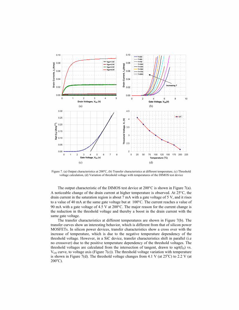
(c) (d) Figure 7. (a) Output characteristics at 200oC, (b) Transfer characteristics at different temperature, (c) Threshold
voltage calculation, (d) Variation of threshold voltage with temperatures of the DIMOS test device
The output characteristic of the DIMOS test device at 200°C is shown in Figure 7(a). A noticeable change of the drain current at higher temperature is observed. At 25°C, the drain current in the saturation region is about 7 mA with a gate voltage of 5 V, and it rises to a value of 40 mA at the same gate voltage but at 100°C. The current reaches a value of 90 mA with a gate voltage of 4.5 V at 200°C. The major reason for the current change is the reduction in the threshold voltage and thereby a boost in the drain current with the same gate voltage. The transfer characteristics at different temperatures are shown in Figure 7(b). The transfer curves show an interesting behavior, which is different from that of silicon power MOSFETs. In silicon power devices, transfer characteristics show a cross over with the increase of temperature, which is due to the negative temperature dependency of the threshold voltage. However, in a SiC device, transfer characteristics shift in parallel (i.e no crossover) due to the positive temperature dependency of the threshold voltages. The threshold voltages are calculated from the intersection of tangent, drawn to sqrt(ID) vs. VGS curve, to voltage axis (Figure 7(c)). The threshold voltage variation with temperature is shown in Figure 7(d). The threshold voltage changes from 4.1 V (at 25oC) to 2.2 V (at 200oC).

Rdrain
RdriftCgd
Cgs
Cds Dbody
D
S
RGIRCHG
Rsource
1
2
3
45
6
7
M1
Figure 8. SPICE model for 4H-SiC DIMOS transistor
4. SPICE Model Development 4.1 SPICE Model: A simple behavioral SPICE model for the SiC DIMOSFET is proposed based on the understanding of the power MOSFET device terminal behavior (Figure 8). The aim of the model development is to reuse the available built-in FET models of the regular lateral MOS devices of the commercial SPICE simulator. The advantage of the model is the limited number of required parameters, which can readily be extracted from simple terminal measurements or from standard datasheets, using the algorithmic and empirical approach as described below. Once the parameters are placed, the model can be used to simulate either p-channel or n-channel SiC power MOSFET devices over a wide range of currents and voltages.
Table IV. Input Listing of the Sub-circuit Model
* This the power DIMOS sub-circuit * Node 1 is the power mos drain * Node 2 is the power mos gate * Node 3 is the power mos source .SUBCKT POWMOS 1 2 3 CGS 2 6 634P CGD 2 1 344P CDS 1 3 207P RDRIFT 5 7 14.33 RDRAIN 1 7 0.1 RSOURCE 3 6 0.1 RG 2 4 1MEG M1 5 4 6 6 DIMOS DBODY 3 1 DMOD1 GIRCH 5 6 2 3 0.001 .MODEL DIMOS NMOS VTO=3.9 KP=9.8E-3 TOX=0.07U L=1.5 W=185 .MODEL DMOD1 D IS=1E-16 RS=70 CJO=407P .ENDS

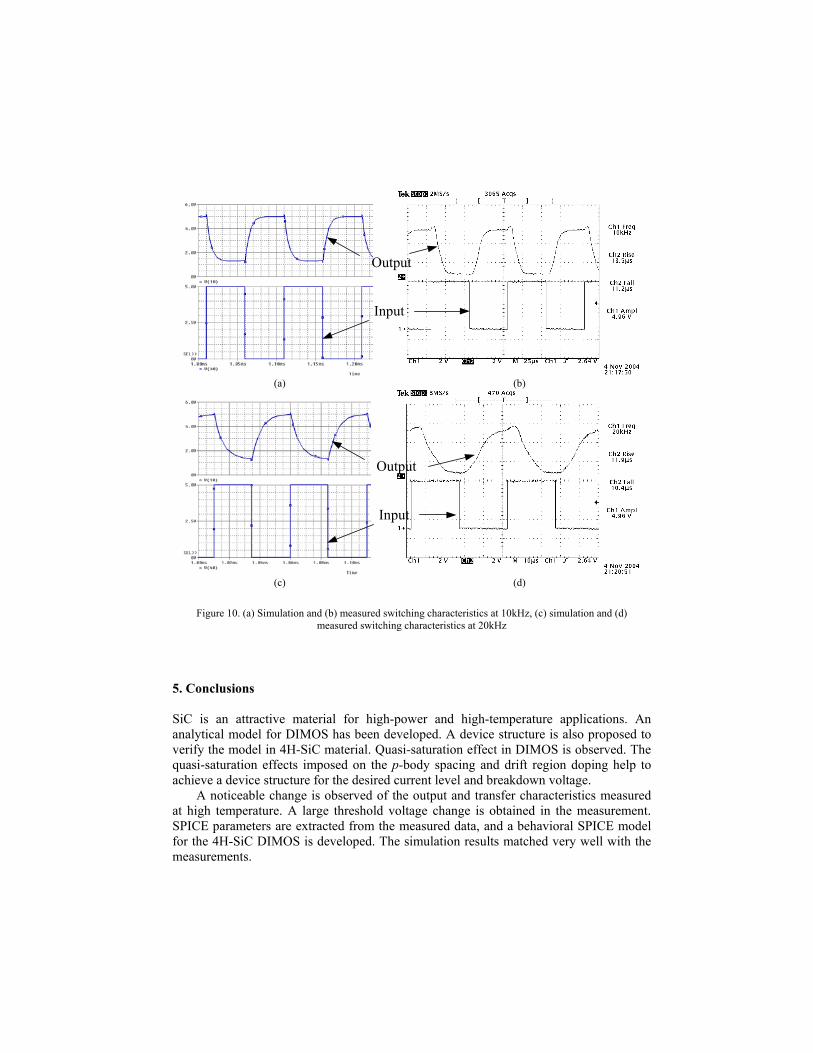
The model especially considers silicon carbide material and process related parameters that affect the device performance. The model can be described as a sub-circuit within the same SPICE code and can be run in any commercial SPICE simulator. Since DIMOS is a power device, its channel length, width, and other device dimensions are big enough to neglect the second order effects in the model equations, and the simulation can be carried out as SPICE level 1 or level 2. Due to larger gate area, power MOSFETs show large gate capacitance. The major three capacitances considered in the model are: gate-source capacitance (CGS), gate-drain capacitance (CGD), and drain-source capacitance (CDS). These capacitances show considerable effects on switching characteristics or dynamic behavior of the device. Power MOSFETs can block the voltage in reverse bias condition. This blocking capability is usually represented by the reverse bias body diode, which is formed between the p-bodies and n-drift region of the vertical structure. The effect of channel resistance variation with gate bias is represented by the dependent current source IRCH. The current from the dependent current source increases with an increase in the gate voltage. The proportionality constant of the dependent current is determined from the empirical fit of the measured data. 4.2 Model Verification: The parameters of the sub-circuit model are extracted from the device terminal characteristic measurements. Table IV shows a listing of the sub-circuit model. A simple chopper circuit is built on a test board to measure the switching characteristics of the test device as shown in Figure 9. An input pulse train of square-wave (0-5V peak-peak) for the frequency range of (1 kHz-50 kHz) is applied to the input, and the corresponding output is observed. The inverter circuit is then simulated using the developed sub-circuit model. The comparison of the simulated wave-shapes to the measured wave-shapes is shown in Figure 10(a,b) and Figure 10(c,d) at 10 kHz and 20 kHz, respectively. The simulation results matched very well with the measurement. It is observed from the switching characteristics that the device can be operated for the frequency range of (0-20 kHz). The SPICE model can be used reliably in circuit simulation at least for the low voltage low power case.
RG
RD
VDD
Input Signal
Output Signal
Deviceunder Test
Figure 9. Inverter circuit used for switching characteristics measurement
Input
Output
(a) (b)
Input
Output
(c) (d)
Figure 10. (a) Simulation and (b) measured switching characteristics at 10kHz, (c) simulation and (d) measured switching characteristics at 20kHz
5. Conclusions SiC is an attractive material for high-power and high-temperature applications. An analytical model for DIMOS has been developed. A device structure is also proposed to verify the model in 4H-SiC material. Quasi-saturation effect in DIMOS is observed. The quasi-saturation effects imposed on the p-body spacing and drift region doping help to achieve a device structure for the desired current level and breakdown voltage. A noticeable change is observed of the output and transfer characteristics measured at high temperature. A large threshold voltage change is obtained in the measurement. SPICE parameters are extracted from the measured data, and a behavioral SPICE model for the 4H-SiC DIMOS is developed. The simulation results matched very well with the measurements.

Acknowledgements This project is supported by ORNL and the U.S. Department of Energy’s Office of Advanced Transportation Technology Freedom Car Research Program. The authors would like to thank Dr. Anant Agarwal and Dr. Sei-Hyung Ryu of Cree Research Inc. for supplying the SiC DIMOSFET sample and necessary information about the device structure. The authors would also like to thank Mr. Madhu Chinthavali of ORNL for help in the high power device measurements and Dr. Ben. Blalock of the University of Tennessee, Knoxville, for providing the high temperature measurement setup for the device characterization at high temperatures. References: 1. A. Powell and L. Rowland, “SiC Materials-Progress, Status, and Potential Roadblocks,” Proc.
IEEE, 2002: 90(6):942-55. 2. A. Elasser and T.P. Chow, “Silicon Carbide Benefits and Advantages for Power Electronics
Circuits and Systems,” Proc. IEEE, 2002: 90(6): 969-86. 3. M. Bhatnagar and B. J. Baliga, “Comparison of 6H-SiC, 3C-SiC, and Si for Power Devices,”
IEEE Trans. on Electron Devices, 40(3), pp. 645-655, March 1993. 4. C. Weitzel, J. Palmour, C. Carter, K. Moore, K. Nordquist, S. Allen, C. Thero, and Bhatnagar,
“Silicon Carbide High-Power Devices”, IEEE Trans. on Electron Devices, vol. 43 no. 10, pp. 1732-1741, October 1996.
5. D. B. Slater, “Development of a high temperature SiC CMOS Technology”, SBIR abstract, Cree Research, Inc. Durham, NC, 1997.
6. J. N. Shenoy, J. A. Cooper, and M.. R. Melloch, “High-Voltage Double-Implanted Power MOSFET’s in 6H-SiC,” IEEE Electron Devices Letters, vol. 18, no. 3, pp. 93-95, 1997.
7. M. Hasanuzzaman and S. K. Islam, “Analytical Modeling of Vertical Double-Implanted Power MOSFET (DIMOS) in 4H-SiC,” Proceedings of Conneticut Symposium on Microelectronics & Optoelectronics, Connecticut, March 2002.
8. B. Ozpineci, L. M. Tolbert, S. K. Islam, T. J. Theiss, “A Parametric Device Study for SiC Diodes in Vehicular Applications,” Proceedings of IEEE Vehicular Technology Conference (VTC02), Vancouver, Canada, September 24-29, 2002, pp. 1495-1499.
9. Y. S. Kim, and J. G. Fossum, “Physical DMOST Modeling for High-Voltage IC CAD,” IEEE Trans. Electron Devices, vol. 37, no. 3, pp.797-803, March 1990.
10. M. Andersson and P. Kuivalainen, “Physical Modelling of Vertical DMOS Power Transistors for Circuit Simulation,” Physica Scripta. vol. T54, pp. 157-158, 1994.
11. K. Shenai, “Effect of P-Base Sheet and Contact Resistances on Static Current-Voltage Characteristics of Scaled Low-Voltage Vertical Power DMOSFETs,” IEEE Electron Devices Letters, vol. 12, no. 6, pp. 270-272, June 1991.
12. M. Darwish, “Study of the Quasi-Saturation Effect in VDMOS Transistors,” IEEE Trans. Electron Devices, vol. 33, no.11, pp. 1710-1716, November 1986.
13. A. Agarwal et al, “The impact of 75mm plus SiC high quality substrates and epitaxial layers on high power semiconductor device rating,” Proc. the European Power Electronics and Applications Conference (EPE), Toulouse, France, September 2-4, 2003.