design, modeling and fabrication of … · design, modeling and fabrication of thermal ......
TRANSCRIPT

DESIGN, MODELING AND FABRICATION OF THERMAL
ACTUATED MICROMIRROR FOR FINE-TRACKING
MECHANISM OF HIGH-DENSITY OPTICAL DATA
STORAGE
DENG XIAOCHONG
NATIONAL UNIVERSITY OF SINGAPORE
2004

DESIGN, MODELING AND FABRICATION OF THERMAL
ACTUATED MICROMIRROR FOR FINE-TRACKING
MECHANISM OF HIGH-DENSITY OPTICAL DATA
STORAGE
DENG XIAOCHONG (B. Eng., Huazhong Univ. of Sci & Tech, P. R. China)
A THESIS SUBMITTED
FOR THE DEGREE OF MASTER OF ENGINEERING
DEPARTMENT OF ELECTRICAL AND COMPUTER ENGINEERING
NATIONAL UNIVERSITY OF SINGAPORE
2004

i
Acknowledgements
I would like to express my earnest thankfulness to my supervisors, Prof. Chong
Tow Chong and Dr. Yang Jiaping, for their guidance and support during the
entire project. Without their patience and encouragement, completion of this
project is very difficult to me. Their invaluable advices and experiences are of
great benefit not only to the research, but also to the attitude towards my life.
Many thanks should go to all the members of MEMS group at DSI. I would like
to extend my gratitude towards Dr. Mou Jianqiang, Dr. Cheng Jian, Mr. Chong
Nyok Boon and Mr. Lu Yi for imparting their valuable knowledge in ANSYS
simulation tool and MEMS microfabrication to me. I would also like to thank Dr.
Li Qinhua and Mr. Kim Whye Ghee for their help in my test work. Great thanks
to Dr. Qiu Jinjun, Mr. Liu Wei, Mr. Liu Tie and Mr. Li Hongliang for their help in
the fabrication work. Many thanks to Singapore Polytechnic Technology Center
for Nanofabrication & materials, for providing the facilities and helpful
instructions in the clean room.
Furthermore, I would also like to express my sincere thanks to all research
scholars especially the students in the fifth floor of DSI building. Their supports
are not only in the valuable discussion of research work, but to my living in the
past two years as well. Great thanks to DSI for providing me two years research
scholarship.
On a personal note, I wish to express my heartfelt appreciation to my family for

Acknowledgements
ii
their constant support during my pursuing the higher degree.

iii
Summary
In this thesis, a novel micromirror actuated by four thermal bi-layer cantilevers
is proposed as a fine-tracking device for high-density optical disk drives (ODD).
Each of the bi-layer cantilevers comprising two material layers with different
thermal expansion coefficients can bend vertically and drive an integrated
micromirror in the out-of-plane motion. In the meanwhile, the movement of
micromirror can be detected by the embedded high-sensitivity piezoresistive
sensors on the cantilevers. To design the bi-layer cantilever design and
modeling, theoretical models are built for thermal-mechanical analysis.
Furthermore, finite-element analysis is performed to evaluate the transient
responses and thermal deformations under the electrical field. The proposed
devices have been fabricated successfully by MEMS technology compatible
with standard IC process. The experimental and simulation results show that a
micromirror of 225µm × 225µm can be vertically moved up 1µm, which is
equivalent to 1.4µm displacement in the track direction of the spinning optical
disk, by a lower driving voltage at 3V with 3mW power consumption. The
embedded piezoresistive sensor is able to detect the micromirror motion by
measuring the resistance change of the cantilever piezoresistive layers. The
resistance change of 0.8Ω is characterized when the micromirror is forced
down 1µm by one probe tip. The measured resonance frequency of 7 kHz for
the micromirror device is high enough to support high bandwidth servo control
in high-density ODD.

i
Table of contents
1. Introduction....................................................................1
1.1. Literature review........................................................................................................ 1
1.2. Motivation ................................................................................................................... 4
1.3. Organization of thesis............................................................................................... 5
2. Background....................................................................7
2.1. Introduction to MEMS............................................................................................... 7
2.2. MEMS actuators...................................................................................................... 10
2.2.1. Piezoelectric actuator ............................................................................... 10
2.2.2. Electrostatic actuator ................................................................................ 11
2.2.3. Thermal actuator ....................................................................................... 12
2.2.4. Electromagnetic actuator ......................................................................... 13
2.3. Micromachining technologies................................................................................ 14
2.4. Optical data storage (ODS) ................................................................................... 15
2.4.1. The optical pick up head .......................................................................... 16
2.4.2. Focus and tracking positioning................................................................ 17
3. Design and modeling.................................................18
3.1. Problem statement and MEMS solutions ............................................................ 18
3.2. Design and numerical analysis ............................................................................. 21
3.2.1. Actuation mechanism ............................................................................... 21
3.2.2. Material selection ...................................................................................... 22
3.2.3. Device design ............................................................................................ 22
3.2.4. Numerical analysis of bi-layer cantilever ............................................... 23
3.3. Finite-element simulation ....................................................................................... 26
3.4.1. FEM modeling............................................................................................ 27
3.4.2. Residual stress induced deflection ......................................................... 27

Table of Contents
ii
3.4.3. Electrothermal analysis ............................................................................ 30
3.4.4. Thermo-Mechanical analysis................................................................... 34
3.4.5. Modal analysis ........................................................................................... 36
3.5. Parametric design analysis.................................................................................... 38
3.6. Summary .................................................................................................................. 41
4. Process development and fabrication ..................40
4.1. Photolithography ..................................................................................................... 40
4.2. Surface silicon micromachining ............................................................................ 41
4.2.1. Thermal oxidation ...................................................................................... 41
4.2.2. PECVD........................................................................................................ 42
4.2.3. RIE............................................................................................................... 43
4.2.4. Sputtering ................................................................................................... 44
4.3. Bulk silicon micromachining .................................................................................. 45
4.3.1. DRIE ............................................................................................................ 45
4.4. Mask layout design and process .......................................................................... 46
4.4.1. Mask layout design ................................................................................... 47
4.4.2. Mask process ............................................................................................. 51
4.5. Device fabrication ................................................................................................... 52
4.5.1. Starting material......................................................................................... 52
4.5.2. Process flow ............................................................................................... 52
4.5.3. Process improvement ............................................................................... 59
4.6. Summary .................................................................................................................. 67
5. Test and calibration....................................................69
5.1. Resistance measurement ...................................................................................... 69
5.2. MEMS mirror displacement measurement.......................................................... 71
5.3. Frequency response ............................................................................................... 74
5.4. Piezoresistive sensing function............................................................................. 76

Table of Contents
iii
5.5. Summary .................................................................................................................. 77
6. Conclusions .................................................................78
References ..............................................................................81
Appendix A .............................................................................88
Appendix B .............................................................................92

iv
List of Figures
Fig. 1-1: 2-D (a) and 3-D (b) MEMS micromirrors [1]......................................................... 2
Fig. 1-2: 1-D MEMS micromirror [2]. ..................................................................................... 2
Fig. 1-3: MEMS tracking mirror structure [9]. ...................................................................... 4
Fig. 1-4: PZT actuated micromirror [10]. .............................................................................. 4
Fig. 2-1: DMD chip schematic system [20]. ......................................................................... 9
Fig. 2-2: The GLV Device with alternate ribbons deflects to form a dynamic diffraction
grating [19]. ....................................................................................................................... 9
Fig. 2-3: Hierarchy of various actuators [21]. .................................................................... 10
Fig. 2-4: Schematic of a piezoelectric actuator. ................................................................ 11
Fig. 2-5: Schematic of an electrostatic actuator. ............................................................... 11
Fig. 2-6: (a) Comb-drive electrostatic microactuator [25]; (b) Electrostatic micromotor
[26]. .................................................................................................................................. 12
Fig. 2-7: Schematic of a thermal pneumatic microactuator. ............................................ 12
Fig. 2-8: Bi-layer thermal microactuator. ............................................................................ 13
Fig. 2-9: Schematic of a magnetic actuator. ...................................................................... 14
Fig. 2-10: Schematic plot of an optical storage drive [32]. .............................................. 15
Fig. 2-11: Schematic of an optical disk system. ................................................................ 16
Fig. 2-12: Data pits recorded on a disk. ............................................................................. 17
Fig. 2-13: the schematic plot of traditional VCM in ODS. ................................................ 18
Fig. 3-1: Fine-tracking optical disk drive............................................................................. 20
Fig. 3-2: Schematic plot of thermal actuated micromirror as a fine tracking device in
ODS ................................................................................................................................. 20
Fig. 3-3: The structure of the thermal actuated micromirror. ........................................... 23
Fig. 3-4: Schematic of a bi-layer structure ......................................................................... 23
Fig. 3-5: 3-D plot of r-1, t1 and t2........................................................................................... 25

List of figures
v
Fig. 3-6: Comparisons between FEM and numerical results. ......................................... 26
Fig. 3-7: Finite element model of the thermal actuator .................................................... 29
Fig. 3-8: The residual stress induced deformation distribution of the actuator............. 29
Fig. 3-9: Applied pulse voltage (500 µs heating + 1500 µs cooling).............................. 31
Fig. 3-10: Voltage distributions by heating pulse voltage. ............................................... 31
Fig. 3-11: Current density distributions by heating pulse voltage. .................................. 32
Fig. 3-12: Derived cantilever temperature with a thermal time constant of
approximately 650µs..................................................................................................... 33
Fig. 3-13: The temperature distributions of the thermal actuator by heating pulse
voltage. ............................................................................................................................ 34
Fig. 3-14: The deformation distributions under the thermal distribution loads. ............ 35
Fig. 3-15: The stress distributions when the micromirror is actuated. ........................... 35
Fig. 3-16: The 1st (a), 2nd (b) and 3rd (c) mode shapes and the resonant frequencies of
the thermal actuator....................................................................................................... 37
Fig. 3-17: Displacements and temperatures versus varying DC voltages. ................... 40
Fig. 3-18: Micromirror displacement versus applied power under DC voltage............. 41
Fig. 4-1: Process flow-chart of photolithography process. .............................................. 41
Fig. 4-2: Schematic of thermal oxidation system. ............................................................. 42
Fig. 4-3: Schematic of PECVD system............................................................................... 43
Fig. 4-4: Schematic of RIE system...................................................................................... 44
Fig. 4-5: Schematic of RF sputtering system. ................................................................... 45
Fig. 4-6: Schematic of DRIE system................................................................................... 46
Fig. 4-7: The schematic plot of the DWL-66 Mask Writer. ............................................... 47
Fig. 4-8: Four masks: (a) Mask #1 (Cantilever oxide layer pattern mask); (b) Mask #2
(Back side release mask); (c) Mask #3 (Cantilever pattern mask); (d) Mask #4
(Mirror and electronical pads mask). .......................................................................... 48
Fig. 4-9: The four mask layouts with alignment markers. ................................................ 50

List of figures
vi
Fig. 4-10: The basic steps in writing a mask. .................................................................... 51
Fig. 4-11: Starting SOI wafer. ............................................................................................... 52
Fig. 4-12: Oxidation. .............................................................................................................. 53
Fig. 4-13: Photolithographic patterning and RIE patterning. ........................................... 54
Fig. 4-14: Backside DRIE patterning. ................................................................................. 54
Fig. 4-15: Topside cantilevers and mirror substrate patterning....................................... 55
Fig. 4-16: Mirror, interconnect lines and pads patterns Lift-off........................................ 56
Fig. 4-17: SEM pictures of topside view before backside release. (a) the top view of
the whole structure. (b) the zoomed picture. ............................................................. 57
Fig. 4-18: Backside release.................................................................................................. 57
Fig. 4-19: SEM picture of released structure with broken hinge..................................... 58
Fig. 4-20: Surface roughness after resist burned. ............................................................ 58
Fig. 4-21: Oxidation. .............................................................................................................. 60
Fig. 4-22: Topside oxide pattern. ......................................................................................... 60
Fig. 4-23: Backside DRIE nearly etching through............................................................. 60
Fig. 4-24: Topside cantilevers and mirror substrate pattern. ........................................... 61
Fig. 4-25: Mirror, interconnect lines and pads patterns Lift-off........................................ 61
Fig. 4-26: Backside release.................................................................................................. 62
Fig. 4-27: Prototype of Design 7.......................................................................................... 63
Fig. 4-28: SEM pictures of Design 7 after testing. ............................................................ 64
Fig. 4-29: SEM pictures of Design 1. .................................................................................. 65
Fig. 4-30: Prototype of Design 2.......................................................................................... 65
Fig. 4-31: Prototype of Design 6.......................................................................................... 66
Fig. 4-32: Prototype of Design 8.......................................................................................... 66
Fig. 5-1: Probe Station and Semiconductor Characterization System. ......................... 70
Fig. 5-2: I-V plot of two cantilevers when applied DC sweep voltage from 0 to 1mV. . 70
Fig. 5-3: The test setup for the actuator. ............................................................................ 71
Fig. 5-4: The test platform for the thermal actuator. ......................................................... 71

List of figures
vii
Fig. 5-5: Experimental data from oscilloscope showing the input square wave and the
output from the mirror deflection with respect to time. ............................................. 73
Fig. 5-6: Deformation results of measurement and simulation. ...................................... 73
Fig. 5-7: The resonant frequency test setup for the actuator. ......................................... 75
Fig. 5-8: The frequency response measurement by external mini-shaker approach. . 75
Fig. 5-9: The output voltage changing when the cantilever is brought down 1µm by the
probe tip. ......................................................................................................................... 77
Fig. 6-1: The modified self-detected thermal actuated micromirror................................ 80

viii
List of Tables
Table 3-1: Design parameters of the thermal microactuator (µm) ................................. 26
Table 3-2: Material properties used in the FEM simulations. .......................................... 28
Table 3-3: Eight parametric design cases of the thermal microactuator (µm).............. 38
Table 3-4: Simulation results of different parameter designs. ......................................... 39

ix
List of Symbols d micromirror movement Δ steered laser movement ΔT cantilever temperature difference σ thermal conductance ξ scaling factor KSi thermal conductivity of silicon L length of the cantilever dA cantilever free end deflection r cantilever bending radius w width of the cantilever ti thickness of layer i Wh width of hinge Lh length of hinge Th thickness of hinge R0 resistance at the room temperature Rht resistance at the rising temperature β temperature coefficient of resistance P rate of heat generation U applied voltage Ei Young’s moduli of layer i αi thermal coefficient of expansion of layer i ∆α difference thermal coefficient of expansion ρ density
Rρ resistivity of the doping silicon layer

List of Symbols
x
c specific heat ν Poisson ration p Resistivity K thermal conductivity

xi
List of publications
1. X. C. Deng, J. P. Yang and T. C. Chong. Design and modeling of thermally
actuated micromirror for fine-tracking mechanism of high-density optical
data storage. International Journal of Computational Engineering Science,
Vol. 4, No. 2, pp.413-416. 2003.
2. J. P. Yang, X. C. Deng and T. C. Chong. A self-sensing thermal actuator
incorporating micromirror for tracking mechanism of optical drive, IEEE
Sensors’04. Vienna, Austria. pp 900-903, Oct.24-27, 2004.
3. J. P. Yang., X. C. Deng and T. C. Chong. An electro-thermal bimorph-based
Microactuator for precise track-positioning of optical disk drives. Journal of
Micromechanics and Microengineering. Vol. 15, pp 958-965, 2005.

1
1. Introduction
1.1. Literature review
Much effort has been made to develop optical mirrors using MEMS technology
because of its distinctive features such as compact size, low cost, low-power
consumption and light weight. There are mainly two types of micromirrors:
torsional micromirrors and translational displacement micromirrors. Torsional
micromirrors include two-dimensional (2-D), three-dimensional (3-D) and
one-dimensional (1-D) approaches.
In the 2-D approach [1] as shown in Fig 1-1 (a), an array of micromirror and
optical fibers are arranged in such a way that the optical plane is parallel to the
surface of the silicon substrate. The micromirror has two states: cross state and
bar state. In the cross state, the mirror moves into the path of the light beam
and reflects the light beam, while in the bar state, it allows the light beam to
pass straight through. One advantage of the 2-D approach is that the
micromirror position is bistable (on or off), which makes them easy to control
with digital logic. In the 3-D approach in Fig. 1-1 (b), the micromirror has two
degrees of freedom, which allows a single micromirror to direct an input light
beam to more than one possible output ports. However, both the 2-D and 3-D
micromirrors have the fiber management problem. To alleviate this problem,
Mechels et al. [2] developed the 1-D micromirros as shown in Fig. 1-2, in which
light leaves the fiber array and is collimated by a lens assembly. A dispersive
element is used to separate the input dense wavelent-division multiplexing
(DWDM) signal into its constituent wavelengths. Each wavelength strikes an

Chapter 1 Introduction
2
individual gold-coated MEMS micromirror, which directs it to the desired output
fiber where it is combined with other wavelengths via the dispersive element.
When integrated with the dispersive element, the 1-D MEMS mirror array
requires only one micromirror per wavelength. Therefore, the switch scales
linearly with the number of DWDM channels. In addiction, the switch can be
controlled with simple electronics in an open-loop configuration because each
micromirror has two stable switching positions. This results in a dramatic
reduction in size, cost and power consumption compared to other MEMS
switching technologies.
(a) (b)
Fig. 1-1: 2-D (a) and 3-D (b) MEMS micromirrors [1].
Fig. 1-2: 1-D MEMS micromirror [2].

Chapter 1 Introduction
3
The torsional micromirrors are also developed as a MEMS tracking mirror in
optical data storage. Watanabe et al. [3] developed a MEMS tracking mirror
used in optical data storage as shown in Fig. 1-3. Compared to electromagnetic
mirrors, this electrostatic MEMS mirror can be produced in large volumes at low
cost. Because it is smaller and lighter, it can be mounted on a coarse positioner
without adversely affecting the fast motion of the positioner. Unlike a traditional
VCM actuator in optical disk drive, this MEMS actuator has no undesirable
mechanical resonance due to its simple mechanical structure. Therefore, it can
support a higher bandwidth of track-following control in high-density optical disk
drives. However, the operation voltage of the electrostatic MEMS actuated
micromirror is about 30V which is too high to be embedded in practical use.
On the other hand, translational displacement micromirrors include in-plane
and out-of-plane mirrors which can be used for display [4], confocal
microscopes [5], optical coherence tomographs [6-7] and optical fiber switch
applications [8-9]. Furthermore, translational displacement micromirrors are
also proposed for fine-tracking mechanism of high-density optical data storage.
Yee et al. [10] developed a Lead Zirconate Titanate (PZT) actuated micromirror.
Bending motions of the metal/PZT/metal unimorphs translate an integrated
micromirror along the out-of-plane direction. Fig. 1-4 shows the Scanning
Electron Microscope (SEM) picture of the device. The micromirror can be
actuated up to more than 5µm under 10V. One disadvantage is that this device
involves complicated PZT fabrication process.

Chapter 1 Introduction
4
Fig. 1-3: MEMS tracking mirror structure [9].
Fig. 1-4: PZT actuated micromirror [10].
1.2. Motivation
The main objective of this study is to design, simulate and fabricate a novel
actuated micromirror used in fine-tracking of optical data storage. The proposed
micromirror should have 1µm displacement, which is equivalent to 1.4µm
displacement in the track direction of the spinning optical disk under very low
voltage. The micromirror should have relatively fast frequency response. In

Chapter 1 Introduction
5
addition, the motion of the micromirror can be self-sensed for close loop
controls. The fabrication process is also expected to be simple and fully
compatible with standard IC process.
1.3. Organization of thesis
The thesis consists of six chapters:
Chapter 1 describes the state-of-art micromirror research and its applications in
optical storage. Following that, the objectives of this thesis work are presented.
Chapter 2 reviews the background and current development of MEMS
technology. Different types of MEMS actuators and micromachining
technologies are introduced. The background of optical data storage is also
summarized.
Chapter 3 proposes a novel MEMS device for fine-tracking mechanism in an
optical pickup module. Numerical analysis is conducted to optimize the
proposed device structure. A series of simulations based on finite element
method (FEM) are carried out to optimize the performances of the MEMS
device. The analyses include residual stress induced deformation analysis,
electrothermal analysis, mechanical analysis and modal analysis.
Chapter 4 investigates various processes associated with photolithography,
bulk and surface silicon micro-machining technologies used in MEMS
fabrication process. The process development and the fabricated MEMS

Chapter 1 Introduction
6
devices are discussed.
Chapter 5 describes the calibration and experimental work of the MEMS
actuator prototypes. The resistance of the actuator device is measured using
probe station and semiconductor characterization system. Static and dynamic
performances are evaluated by Laser Doppler Vibrometer (LDV) and compared
with the simulation results. The self-sensing function is characterized by
detecting resistance change of two cantilevers in series.
Chapter 6 summarizes the research work. Several research areas are
proposed for future improvement.

7
2. Background
2.1. Introduction to MEMS
MEMS is the acronym for micro-electro-mechanical systems. In Europe, it is
called Microsystems technology (MST). In Japan, the technology is also called
micromachines. A MEMS contains components of sizes in 1 micrometer (µm) to
1 millimeter (mm), (1mm=1000 µm). A MEMS is constructed to achieve a
certain engineering function or functions by electromechanical or
electrochemical means [11]. Someone defines MEMS as [12]:
It is a portfolio of techniques and processes to design and create miniature
systems;
It is a physical product often specialized and unique to a final
application-one can seldom buy a generic MEMS product at the
neighborhood electronics store;
“MEMS” is a way of making things, reports the Microsystems Technology
Office of the United States Defense Advanced Research Program Agency
(DARPA) [13]. These “things” merge the functions of sensing and actuation
with computation and communication to locally control physical parameters
at the microscale, yet cause effects at much grander scales.
Although there is not a universal definition, MEMS products possess a number
of distinctive features. They are miniature embedded systems involving one or
many micromachined components or structures. They enable higher level

Chapter 2 Background
8
functions. They integrate smaller functions into one package for greater utility.
They can also bring cost benefits [12].
With the strong financial support from both governments and industries, MEMS
research has achieved remarkable progress. MEMS technology has proven its
outstanding and revolutionary capability in many different fields such as inertial
measurement, microfluidics, optics, pressure measurement, RF devices and
other devices. Today MEMS is a $3 billion business and is projected to grow at
a compound annual growth rate (CAGR) of 40% per year through 2004 [14].
There are several examples of commercially successful MEMS devices. One
notable example is the evolution of crash sensors for airbag safety systems [12].
This type of accelerometers is based on techniques and designs originally
developed at the University of California, Berkeley. Analog Devices has
integrated a MEMS accelerometer with bipolar complementary metal oxide
semiconductor (Bi-CMOS) processing on a single chip to build their ADXL50
[15].
MEMS based projection display system is another exciting example [16]. Two
basic approaches are now in use: reflective displays named Digital Micromirror
Device (DMD), pioneered by Texas Instruments [17], and diffractive displays
named Grating Light Valve (GLV), pioneered by Silicon Light Machines [18-19].
When a DMD chip is coordinated with a digital video or graphic signal, a light
source and a projection lens, its mirrors can reflect an all-digital image onto a
screen or other surface. The DMD and the sophisticated electronics that

Chapter 2 Background
9
surround it are called Digital Light Processing™ technology (DLP) [20]. Fig. 2-1
shows the schematic plot of DLP system. Instead of using a mirror to reflect the
light, GLV device has an array of alternate deflected ribbons which form a
dynamic diffraction grating to form pixel of image. Fig. 2-2 shows the schematic
plot of GLV Device.
Fig. 2-1: DMD chip schematic system [20].
Fig. 2-2: The GLV Device with alternate ribbons deflects to form a dynamic diffraction grating [19].

Chapter 2 Background
10
2.2. MEMS actuators
Microactuator is one of the key devices to provide the driving force for the
MEMS system to perform physical functions. It provides the driving force and
motion for these MEMS based devices. Fig. 2-3 shows typical actuators
including piezoelectric, electrostatic, thermal and magnetic actuators according
to actuation principles.
Fig. 2-3: Hierarchy of various actuators [21].
2.2.1. Piezoelectric actuator
A beam with deposited piezoelectric material film will deform when a voltage is
applied across a piezoelectric film. Fig. 2-4 shows a schematic plot of
piezoelectric actuator. Piezoelectric actuator has high resolution, good
response and large force. However, it suffers from small strain, hysteresis and
drift [22].

Chapter 2 Background
11
Fig. 2-4: Schematic of a piezoelectric actuator.
2.2.2. Electrostatic actuator
For an electrostatic actuator, electrostatic force will be created when applying
voltage across a simple parallel-plate. The schematic plot of this kind of
actuator is shown in Fig. 2-5. Usually the two plates are separated by dielectric
material such as air.
Fig. 2-5: Schematic of an electrostatic actuator.
The electrostatic actuator is one of the most popular microactuators in MEMS
applications. There are two types of typical electrostatic actuators: comb-drive
microactuators [23] and wobble microactuators [24]. Fig. 2-6 shows SEM
pictures of these two electrostatic microactuators. Generally, high driving
voltage and small gap between the two plate is needed to create enough forces
for an electrostatic actuator [22].
+
_
V
Moveable plate
V
Constraint base
Silicon cantilever beam
Piezoelectric crystalElectrodes

Chapter 2 Background
12
(a) (b)
Fig. 2-6: (a) Comb-drive electrostatic microactuator [25]; (b) Electrostatic micromotor [26].
2.2.3. Thermal actuator
Thermal actuation has been extensively employed in MEMS. It includes a
broad spectrum of principles such as thermal pneumatic, shape memory alloy
(SMA) effect and bimetal effect [27].
Thermal pneumatic microactuator relies on the expansion of liquid or gas to
create the actuation. Fig. 2-7 shows a cavity containing a volume of fluid, with a
thin membrane as one wall. Current passed through the heating resistor causes
the liquid in the cavity to expand to deform the membrane.
Fig. 2-7: Schematic of a thermal pneumatic microactuator.
Heating element
Liquid
Membrane
Heated Liquid

Chapter 2 Background
13
The mechanism of actuation in SMA effect is that a temperature-induced phase
change produces a deformation when heating above the transformation
temperature.
A thermal bimetallic microactuator consists of two different layers with different
coefficient of thermal expansion (CTE). Deformation is generated when the
bi-layer is heated. Fig. 2-8 shows the schematic plot of a thermal bi-layer
actuator. The detailed information on thermal microactuator is introduced in
Chapter 3. Due to heating and cooling procedure, the response of this kind of
actuator is relatively low compared to PZT actuator.
Fig. 2-8: Bi-layer thermal microactuator.
Except the bi-layer thermal actuator, single layer in-plane and out-of-plane
thermal actuators are also used to prevent the delamination problem of the
bi-layer actuator [28-29].
2.2.4. Electromagnetic actuator
Magnetic actuator is often fabricated by electroplating techniques using nickel
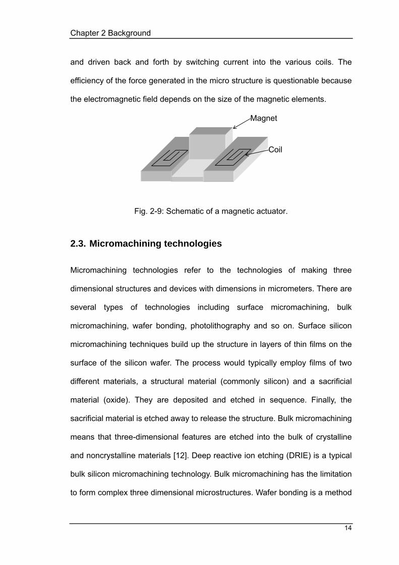
which is a ferromagnetic material. A schematic plot of magnetic actuator
structure is shown in Fig. 2-9. The magnetic resting in the channel is levitated
Heating
Lay 1
Lay 2
Chapter 2 Background
14
and driven back and forth by switching current into the various coils. The
efficiency of the force generated in the micro structure is questionable because
the electromagnetic field depends on the size of the magnetic elements.
Fig. 2-9: Schematic of a magnetic actuator.
2.3. Micromachining technologies
Micromachining technologies refer to the technologies of making three
dimensional structures and devices with dimensions in micrometers. There are
several types of technologies including surface micromachining, bulk
micromachining, wafer bonding, photolithography and so on. Surface silicon
micromachining techniques build up the structure in layers of thin films on the
surface of the silicon wafer. The process would typically employ films of two
different materials, a structural material (commonly silicon) and a sacrificial
material (oxide). They are deposited and etched in sequence. Finally, the
sacrificial material is etched away to release the structure. Bulk micromachining
means that three-dimensional features are etched into the bulk of crystalline
and noncrystalline materials [12]. Deep reactive ion etching (DRIE) is a typical
bulk silicon micromachining technology. Bulk micromachining has the limitation
to form complex three dimensional microstructures. Wafer bonding is a method
Magnet
Coil

Chapter 2 Background
15
for firmly joining two wafers to create a stacked wafer layer for 3-D
microstructures [16]. Photolithography is a basic technology for transferring
patterns onto a substrate. These micromachining technologies are described in
details in Chapter 4.
2.4. Optical data storage (ODS)
Storage density and capacity requirements are growing at an exponential rate
in recent years. Recent developments in portable consumer devices call for
storage system solutions using compact drive units and cheap storage media.
Storage capacities of several hundred Megabytes or even more are necessary
for digital movie or photo recording. HDD and solid state storage are now being
incorporated in PDA’s, camcorders and digital photo cameras. A disadvantage
of these storage solutions is the relatively high cost of the storage media per
Megabyte (MB) and the absence of ROM media for distribution of read-only
data [30]. Optical storage offers a reliable and removable storage medium with
excellent robustness and archival lifetime at very low cost [31]. Fig. 2-10 shows
a schematic plot of an optical storage drive.
Fig. 2-10: Schematic plot of an optical storage drive [32].

Chapter 2 Background
16
2.4.1. The optical pick up head
Fig. 2-11 shows the schematic diagram of a typical optical pickup head [33].
The laser from a semiconductor laser diode is collimated and directed toward a
high-numerical-aperture objective lens. The objective brings the light to
diffraction-limited focus on the surface of the spinning disk, where information is
written to or read from a given track. In the return path, a beam splitter directs
the beam toward one or more detectors, where the recorded information as well
as focusing and tracking-error signals are extracted.
Fig. 2-11: Schematic of an optical disk system.
The recording layer contains spiral tracks of mark patterns that differ in
reflectivity from the area between the marks as shown in Fig.2-12. The reflected
light level changes as the focused laser beam passes over a mark. The beam
splitter senses these changes in the reflected light level and is responsible for
directing a portion of the reflected light onto the photo detector. The detector
current, which is a representation of the mark pattern, is decoded to produce
digital information.
Beam Splitter

Chapter 2 Background
17
Fig. 2-12: Data pits recorded on a disk.
2.4.2. Focus and tracking positioning
The current focus and tracking approach is to use a voice-coil-motor (VCM) to
move the objective lens. The actuator for focus and tracking positioning of
optical disk drives are typically biaxial electromagnetic devices. Two pieces of
permanent magnets are used to form a magnetic circuit. A moving coil is placed
surrounding the centre core of the magnetic circuit. When a current is supplied
to the coil, it will move the coil in a direction which is determined by the current
flowing direction of the coil. As this coil is fixed on the lens holder, the coil
movement will be transferred to the lens.
Laser spot Data pit length
Track grooves

Chapter 2 Background
18
Fig. 2-13: the schematic plot of traditional VCM in ODS.
Spindle Motion
Coils
Magnets
Tracking direction
Linear Guide
Optical Lens

18
3. Design and modeling
In this chapter, a novel MEMS based mirror for an optical pickup module is
designed. Numerical analysis is carried out to optimize the performance of the
MEMS device. A series of FEM simulations are performed to characterize the
MEMS device, including residual stress induced deformation analysis,
electrothermal analysis, mechanical analysis and modal analysis.
3.1. Problem statement and MEMS solutions
Many MEMS based approaches have been proposed in high-density optical
data storage recently. Modified atomic force microscope (AFM) [35], scanning
near-field optical microscope (SNOM) probe [34] and solid immersion lens (SIL)
[36] are all good examples of state-of-art researches. Nevertheless, these
approaches have been mainly focused on the attainable bit size. Optical data
storage, which is one of mainstream storage technologies, also has its
development bottlenecks. In conventional far-field optical data storage such as
compact disk (CD) or digital versatile disk (DVD), a fundamental limitation on
the recordable bit size is determined by the diffraction property of the pickup
optics. This limitation, however, could be overcome by an optical near-field
technique [37]. The bit dimension in optical recording media could be further
reduced using super resolution techniques in magneto optical recording
materials [38].
Another key challenge is to precisely position the optical pickup probe well
below the track pitch of high-density storage media. MEMS, as one enabling
Chapter 3 Design and modeling
19
technology, provides competitive solutions to a fine-tracking mechanism of
high-density magnetic data storage [39]. The optical pickup has potential merits
over the other methods in tracking speed because it is basically non-contact
system. In terms of the tracking speed and the power consumption, it will be
more efficient to steer the laser beam itself as tracking strategy rather than
actuate the whole optic pickup module. The steered laser beam does not apply
any load on the actuator. Furthermore, the device based on the MEMS
technologies can be micro-fabricated to increase the tracking speed [10].
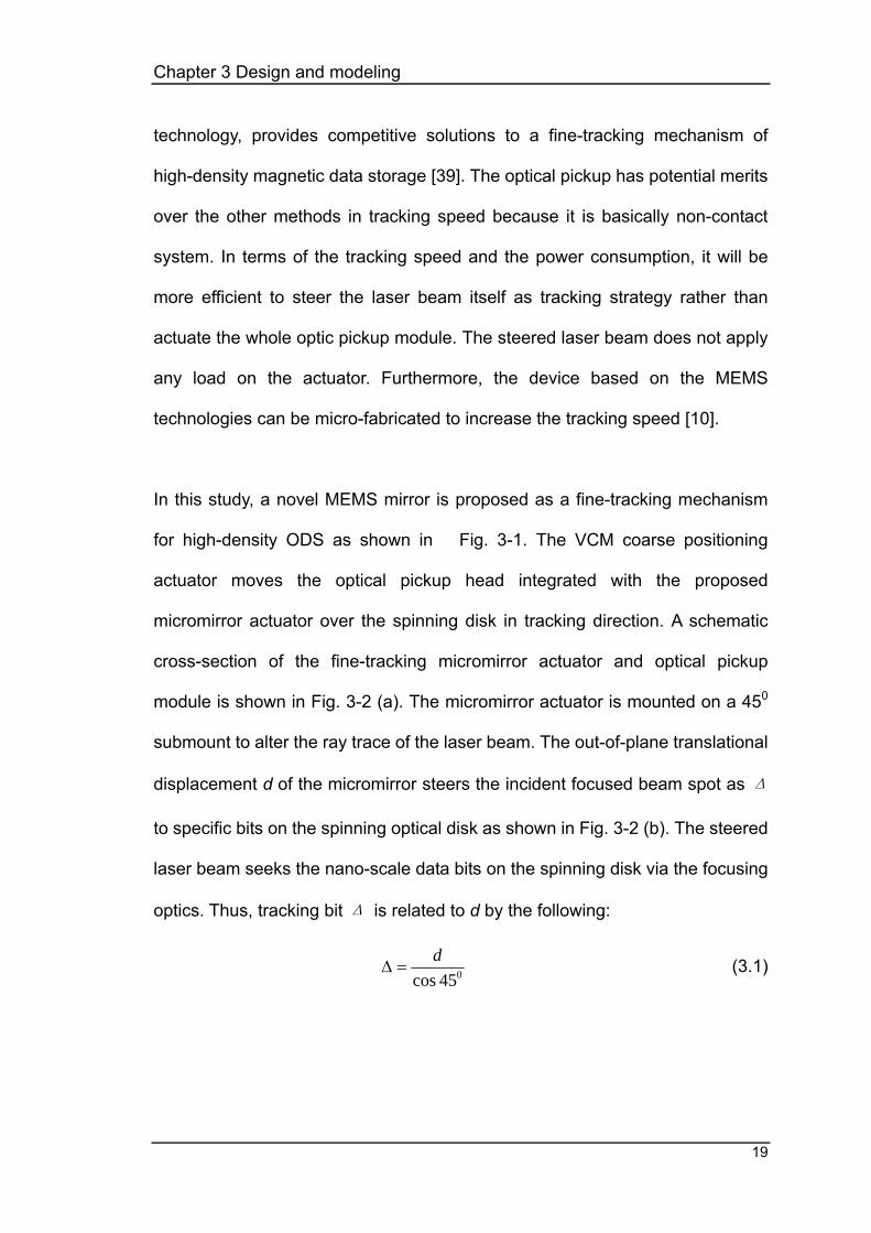
In this study, a novel MEMS mirror is proposed as a fine-tracking mechanism
for high-density ODS as shown in Fig. 3-1. The VCM coarse positioning
actuator moves the optical pickup head integrated with the proposed
micromirror actuator over the spinning disk in tracking direction. A schematic
cross-section of the fine-tracking micromirror actuator and optical pickup
module is shown in Fig. 3-2 (a). The micromirror actuator is mounted on a 450
submount to alter the ray trace of the laser beam. The out-of-plane translational
displacement d of the micromirror steers the incident focused beam spot as Δ
to specific bits on the spinning optical disk as shown in Fig. 3-2 (b). The steered
laser beam seeks the nano-scale data bits on the spinning disk via the focusing
optics. Thus, tracking bit Δ is related to d by the following:
045cosd
=∆ (3.1)

Chapter 3 Design and modeling
20
Fig. 3-1: Fine-tracking optical disk drive.
(a): Micromirror actuator and optical pickup.
(b): the principle of steering the laser bean by micromirror actuator
Fig. 3-2: Schematic plot of thermal actuated micromirror as a fine tracking device in ODS
Fine-tracking micromirror actuator and optical pickup
Optical Disk
VCM
Coarse track positioning by
VCM
45o submount
Laser beam
Micromirror actuator
Optical disk
Focusing Optics
Spinning direction
45o
dΔ
Laser beam
Micromirror actuator

Chapter 3 Design and modeling
21
3.2. Design and numerical analysis
3.2.1. Actuation mechanism
Driving force, speed and power consumption are key factors to be considered
in designing a MEMS actuator. Thermal, electromagnetic, piezoelectric and
electrostatic actuators are commonly used. Although electromagnetic force is
popular in the macro world, the efficiency of the force generated in the micro
structure is questionable because the electromagnetic field depends on the
size of the magnetic elements [40] and manufacturing methods. Piezoelectric
actuation has high resolution, fast response and large force. However, it suffers
from small total strain, hysteresis and drift [22]. Piezoelectric actuator devices
also require more complicated fabrication process. Electrostatic actuators need
higher operating voltages that are not suitable for portable optical drives. In this
study, a thermal microactuator is proposed for the following advantages [41]:
The beam deflection is directly coupled with the dissipated electrical power
and, therefore, the device can be operated at standard microelectronic
voltage levels;
Low voltage operation condition can drive mirror the desired out-of-plane
displacement of 1µm for 1.4µm tracking movement;
The embedded piezoresistive sensor is able to detect the micromirror
motion by measuring the resistance change of the cantilever piezoresistive
layers.
The device fabrication process is simple and fully compatible with standard
IC process.

Chapter 3 Design and modeling
22
3.2.2. Material selection
The thermal microactuator described here is based on the so-called bimetal
effect [42] used extensively for the fabrication of temperature-controlled
electrical switches. Typical thermal actuator consists of a Si-metal sandwich
layer and an integrated polysilicon heating resistor as a driving element.
Riethmü and Benecke [41] have investigated different combinations of
bimorphic layers. Silicon-aluminum (Si-Al) integrated polysilicon heating
resistor is used in many thermal excited microactuators [43-44]. Jerman [45]
and Buser [46] used Si-Al directly as heating resistors. This considerably
simplifies the fabrication process and also the structure itself. Although Si-Al
has a rather high conversion coefficient, high temperature may degrade the
aluminum and cause undesirable creep effect. In this study, doping Si and Si
dioxide bi-layer is used to simplify the fabrication process and the structure. The
doping Si layer is also the heat source resistor and piezoresistive sensor.
Furthermore, the metal degrade problem can be avoided using these bi-layer
materials.
3.2.3. Device design
The device structure of the proposed thermal actuated micromirror is illustrated
in Fig. 3-3. Four identical bi-layer cantilevers located symmetrically around the
mirror periphery suspend a gold-coated micromirror plate by four hinges linking
with the plate. Each cantilever comprises doping Si and Si dioxide layers. Due
to bimorph effect, the cantilevers bend upwards the micromirror plate through
the hinges in the out-of-plane direction when applying voltage to the pads.

Chapter 3 Design and modeling
23
Fig. 3-3: The structure of the thermal actuated micromirror.
3.2.4. Numerical analysis of bi-layer cantilever
Fig. 3-4 shows the schematic plot of one bi-layer cantilever used in the thermal
actuated micromirror in Fig. 3-3. It is obvious that the maximum deflection of the
cantilevers by different thermal expansion coefficients at free end A is the key
performance indicator of the proposed thermal actuator.
Fig. 3-4: Schematic of a bi-layer structure
a
Gold mirror, pad and interconnect line
Si substrate
Si dioxide (top) & doping Si (bottom) bi-layer cantilever
Hinge
1_ Si dioxide
2_ doping Si
w
A

Chapter 3 Design and modeling
24
The deflection dA of cantilever at free end when uniformly heated is [47]:
rLd A 2
2
= (3.2)
where L is the length of the cantilever and r is the bending radius of bi-layer
cantilever due to temperature change:
TttttEEttttttEEtEtEr
∆∆+++++
=α)(6
)232(2)()(
212121
2221
212121
2222
2211 (3.3)
where ΔT is the temperature difference, Ei is Young’s moduli of the layer i,
∆α=α1-α2, αi is the thermal coefficient of expansion for the layer i and ti is the
thickness of the layer i (i=1,2, refer to Si dioxide and doping Si layers,
respectively).
According to the qualitative analysis of Equations (3.2-3.3), the bending radius r
has a minimum value when the two layers have nearly identical geometries and
the same order of Young’s moduli are of the same order. The maximum
deformation will be obtained if ∆α and L are as large as possible, while t1 and t2
are as small as possible. In this work, doping Si and Si dioxide bi-layer
cantilever structure is optimally selected for better values of ∆α with relative
low working temperature.

Chapter 3 Design and modeling
25
Fig. 3-5 displays that maximum dA. is obtained if t1 and t2 could tend to zero.
The deflection decreases dramatically if t1 and t2 are above 2µm. In
consideration of fabrication capability and reliability, the doping Si thickness of
2µm is determined. Furthermore, FEM and numerical results are well compared
as shown in Fig. 3-6, where Doping Si layer thickness t2 is fixed at 2 µm and the
cantilever length is 500 µm. For simplification, it is also assumed that the
temperature distributions are uniform in the cantilever and that the Young’s
Moduli of the materials are constant with temperature. The comparison results
indicate that deflections dA tend to the maximum value when t1 is between
1.4µm and 1.6 µm. Therefore, Si dioxide layer thickness t1 is set to 1.5µm and
the sputtered gold mirror thickness is selected to be 80nm [10].
Fig. 3-5: 3-D plot of dA, t1 and t2.
t1 (µm) t2 (µm)
dA

Chapter 3 Design and modeling
26
Fig. 3-6: Comparisons between FEM and numerical results.
The dimension of the supporting doping silicon substrate beneath the
micromirror is 250µm × 250µm. The bulk micromachined silicon periphery
serves as the anchor of the bi-layer cantilever unimorphs. The detailed design
parameters are given in Table 3-1.
Table 3-1: Design parameters of the thermal microactuator (µm)
Cantilever Hinge
Mirror Length (L)
Width(W)
Doping Si
layer (t1)
Si dioxide layer (t2)
Length(Lh)
Width (Wh)
Thickness(Th)
225×225×2 500 40 2 1.5 30 10 2
3.3. Finite-element simulation
In the above analytical calculation, the hinges and the mirror structures are not
included. The device temperature distributions are not considered either. For
accurate prediction analysis, FEM simulation is required for better evaluation of
dA
t1 0.0 0.5 1.0 1.5 2.0 2.5 3.00
1
2
3
4
5
Def
orm
atio
n(µm
)
Si dioxide layer thickness (µm)
FEM
Numerical
Chapter 3 Design and modeling
27
the device performance. For illustrative purpose, the FEM simulation results of
one typical example as shown in Table 3-1 are given in the following sections.
3.4.1. FEM modeling
FEM is a numerical technique for obtaining an approximate solution to
differential equations [48]. Since the start of the 1970s, FEM has become a very
powerful tool for a wide variety of engineering computational applications. Many
commercial FEM software packages such as ABACUS®, NASTRAN® and
ANSYS® were originated in 1970s. In this study, ANSYS® Multiphysics package
[49] is used to perform the FEM analysis of device. Modeling is divided into four
steps: (1) The static deformation analysis is conducted to get the deflection
distributions resulting from the residual stress; (2) The electro-thermal analysis
is performed to calculate the temperature distributions under the applied
electrical field; (3) The thermo-mechanical analysis by the temperature
distributions loads is conducted to obtain the deflection distributions; and (4)
Modal analysis is carried out to get its mechanical resonance frequencies.
3.4.2. Residual stress induced deflection
Residual stress is one of the important factors which affect the device
performance. The static deformation analysis is performed to evaluate the
residual stress effect.
The residual stress in the oxide layer is greatly dependent on process
parameters such as deposition temperature, oxide layer thickness and
deposition method. It is assumed that the residual stress in the oxide layer is

Chapter 3 Design and modeling
28
constant. 150MPa (compressive) residual stress is used in the modeling [50].
Material properties used in the FEM simulations are shown in Table 3-2. Fig.
3-7 is a finite element model generated using ANSYS®, Solid 45 element. The
degree of freedom (DOF) of four cantilevers at the fixed ends is set to zero. The
simulation results reveal that the residual stress induced deformation of the
micromirror is about 6.5 µm as shown in Fig. 3-8. Although residual stress
causes initial deformation, it does not significantly affect the mirror deformation
caused by thermal actuation mechanism. Thus, residual stress will not be
considered in the further simulation work for simplification.
Table 3-2: Material properties used in the FEM simulations.
Materials Doping Si Si dioxide Gold (Au)
E Modulus (MPa) 1.60E+5 0.70E+5 0.78E+5
ν Poisson radio 0.17 0.17 0.44
ρ Density (kg/µm3) 2.42E-15 2.66E-15 19.30E-15
c Specific heat (pJ/(kg)( ok)) 7.12E+14 10.00E+14 1.29E+14
p Resistivity (TΩ µm) 3.46E-11 1.00E+10 2.20E-14
α Coefficient of thermal expansion (/ok)
2.60E-6 0.50E-6 1.42E-5
K Thermal conductivity (pW/(µm)( ok))
1.48E+8 1.04E+6 3.15E+8

Chapter 3 Design and modeling
29
Fig. 3-7: Finite element model of the thermal actuator
Fig. 3-8: The residual stress induced deformation distribution of the actuator.
Si dioxide
Au mirror and interconnect line

Chapter 3 Design and modeling
30
3.4.3. Electrothermal analysis
In the electrothermal analysis, Solid 69 element is used to build the FEM model
due to its thermal and electrical conduction capability. The temperature of the
four cantilevers at the fixed ends is assumed at room temperature (20). An
input voltage is applied to the four fixed ends. Transient analysis is performed
to obtain thermal time constant which determines the thermal actuator
response speed. A 3V, 500µs heating periodic pulse shown in Fig. 3-9 is
applied across the thermal actuator. Generally, heat transfer modes include: (1)
Conduction to the substrate and the surrounding air, (2) Natural convection and
(3) Natural radiation. However, convection and radiation were found to have
negligible effects [44] and are thus omitted from subsequent modeling to
reduce computational time.
The voltage distributions and current density distributions during heating are
calculated as shown in Fig. 3-10 and 3-11, respectively. The maximum current
density of 0.47E+9pA/(µm)2 is located at the interconnect line part. The derived
temperatures in Fig. 3-12 show that the thermal actuator has a thermal time
constant of approximately 650µs. The temperature distributions of the thermal
actuator during heating are shown in Fig. 3-13, where the maximum
temperature is at 99.2 in the central part of the cantilevers.

Chapter 3 Design and modeling
31
Fig. 3-9: Applied pulse voltage (500 µs heating + 1500 µs cooling)
Fig. 3-10: Voltage distributions by heating pulse voltage.
(s)
V
(V)

Chapter 3 Design and modeling
32
Fig. 3-11: Current density distributions by heating pulse voltage.
(pA/(µm2))

Chapter 3 Design and modeling
33
Fig. 3-12: Derived cantilever temperature with a thermal time constant of approximately 650µs.
Thermal time constant
(s)
650µs

Chapter 3 Design and modeling
34
Fig. 3-13: The temperature distributions of the thermal actuator by heating
pulse voltage.
3.4.4. Thermo-Mechanical analysis
ANSYS® Solid 45 element is again used in the thermo-mechanical analysis.
The temperature distributions resulting from the above electro-thermal analysis
are used as a state variable boundary condition for the current
thermo-mechanical analysis. In addition, the degree of freedom (DOF) of four
cantilevers at the fixed ends is set to zero. Fig. 3-14 shows the deformation
distributions of the device under the temperature distribution loads. It is seen
that the micromirror can be vertically actuated to 1µm. Furthermore, the stress
distributions during actuation show that the maximum stress of 160MPa is
concentrated on the linkages between the hinges and the mirror plate as
revealed in Fig. 3-15. However, no significant change in stress level is found in
()

Chapter 3 Design and modeling
35
the micromirror if the non-uniform stress is not initiated in micromirror itself. This
means that the mirror could be very flat and has no bending under the
temperature distribution loads.
Fig. 3-14: The deformation distributions under the thermal distribution loads.
Fig. 3-15: The stress distributions when the micromirror is actuated.
(MPa)
(µm)

Chapter 3 Design and modeling
36
3.4.5. Modal analysis
Modal analysis is to determine the vibration characteristics, which include the
mechanical resonance frequencies and mode shapes of the thermal actuated
mirror. The FEM model of thermo-mechanical analysis is also used in the
modal analysis. Fig. 3-16 shows the first three mode shapes and resonance
frequencies. The first mechanical resonance frequency is at 12.2 KHz, which is
high enough to support high bandwidth servo control.

Chapter 3 Design and modeling
37
(a)
(b)
(c)
Fig. 3-16: The 1st (a), 2nd (b) and 3rd (c) mode shapes and the resonant frequencies of the thermal actuator.
12.2 KHz
24.9 KHz
26.9 KHz

Chapter 3 Design and modeling
38
3.5. Parametric design analysis
To optimize the bi-layer cantilever performance, parametric design cases as
shown in Table 3-3 are studied to investigate the effect of hinge on the
movement of the mirror. Among them, Design 7 is the illustrate example like in
the section 3.4.
Table 3-3: Eight parametric design cases of the thermal microactuator (µm)
Design number
Hinge width (Wh)
Hinge length(Lh)
Cantilever width (W)
Cantilever length (L)
1 5 30 40 350
2 8 30 40 350
3 10 30 40 350
4 5 20 40 350
5 8 20 40 350
6 10 20 40 350
7* 10 30 40 500
8 20 80 80 800
*: Design 7 is an illustrative example in FEM simulation analysis.
To simplify the simulation process, electrothermal static analysis is performed
to obtain the temperature, deformation and stress distributions under 3V direct
current (DC) instead of the pulse voltage as given in Fig. 3-9. Nevertheless, the
thermal time constants are still calculated through transient analysis when
applying 3V, 500µs heating periodic pulse. The results are listed in Table 3-4. It
is noted that the actuator for Design 7 could be vertically actuated to 0.99 µm

Chapter 3 Design and modeling
39
under 3V DC, which is nearly the same as 1.04 µm under 3V, 500µs heating
periodic pulse. However, the maximum temperature and stress are 238 and
400MPa, respectively, which are different from the pervious transient simulation
results of 100 and 160MPa in Figs. 3-13 and 3-15. The reason is that DC is a
constant voltage while pulse voltage is a discontinuous voltage. Therefore, the
derived temperature distributions of the device are different, which results in the
different stress distributions.
Table 3-4 also reveals that longer cantilevers, longer and narrower hinges will
lead to larger deformation but longer thermal time constant. However, narrow
hinges will decrease the device yield. Therefore, Design 7 is selected as a good
candidate because it could have relative high yield and meets the deformation
requirement (1µm).
Table 3-4: Simulation results of different parameter designs.
Results when applying 3 VDC Results when
applying 500µs heating pulse
Design number Maximum
Deformation (µm)
Maximum Temperature()
Resonance frequency(
KHz)
Maximum Stress (MPa)
Thermal time constant (µs)
1 2.117 239.0 18.60 357.7 450
2 1.494 238.8 20.10 356.1 450
3 1.367 238.7 20.78 402.3 450
4 1.469 239.0 19.78 357.6 450
5 0.980 238.8 21.30 356.1 450
6 0.910 238.7 22.00 400.8 450
7 0.990 238.0 12.00 400.5 650
8 5.650 238.7 6.68 989.5 850
Chapter 3 Design and modeling
40
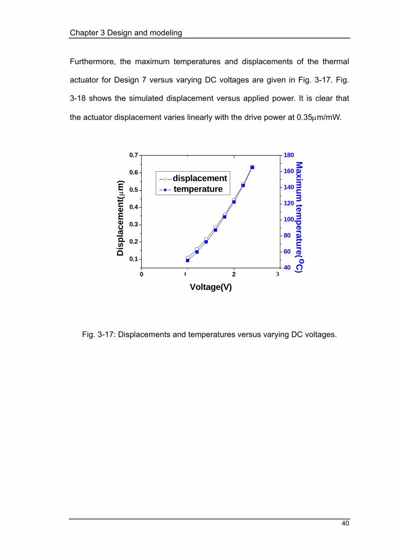
Furthermore, the maximum temperatures and displacements of the thermal
actuator for Design 7 versus varying DC voltages are given in Fig. 3-17. Fig.
3-18 shows the simulated displacement versus applied power. It is clear that
the actuator displacement varies linearly with the drive power at 0.35µm/mW.
0 2
0.1
0.2
0.3
0.4
0.5
0.6
0.7
displacement temperature
Voltage(V)
Dis
plac
emen
t(µm
)
40
60
80
100
120
140
160
180 Maxim
um tem
perature( oC)
Fig. 3-17: Displacements and temperatures versus varying DC voltages.
1 3

Chapter 3 Design and modeling
41
0.2 0.4 0.6 0.8 1.0 1.2 1.4 1.6 1.8 2.0
0.1
0.2
0.3
0.4
0.5
0.6
0.7
Dis
plac
emen
t(µm
)
Power(mW)
Fig. 3-18: Micromirror displacement versus applied power under DC voltage.
3.6. Summary
In this chapter, a MEMS electrothermal actuator integrated with micromirror is
designed, simulated and optimized.
Analytical model is used to optimize the thickness of doping Si layer and Si
dioxide layer. To optimize the device structure, eight parametric design cases
are investigated by: (1) residual stress induced deformation analysis; (2)
electrothermal analysis; (3) thermal-mechanical analysis; and (4) modal
analysis. Design 7, as an illustrative example is described in details to predict
the performance of the device.
The FEM simulation results show that the micromirror could be vertically

Chapter 3 Design and modeling
42
actuated to 1.04 µm under 3V, 500µs heating periodic pulse. The first
mechanical resonance frequency of the micromirror is at 12.2 kHz.
40
4. Process development and fabrication
In this chapter, various fabrication processes associated with photolithography,
bulk and surface silicon micromachining technologies are firstly introduced.
Following that, the proposed micromirror actuator fabrication process is
described. Finally, the fabricated micromirror prototypes are discussed.
4.1. Photolithography
Photolithography is a basic technique to transfer patterns onto a substrate.
Patterns are first transferred to an imageable photo resist (PR) layer which is
exposed with a mask and developed into a selectively patterned layer for
subsequent processing. The basic steps in the photolithography process are
illustrated in Fig. 4-1. Surface preparation includes cleaning of the wafer and
dehydration to remove water from the surface of the wafer.
Hexamethyldisilazane (HMDS) is also used to enhance the adhesion between
the resist and the wafer surface. The wafer is then coated with PR which is
sensitive to ultraviolet light. Pre-baking with hotplate evaporates the solvents in
the resist. Alignment and exposure are then performed to transfer the pattern of
the mask to the resist. The ultraviolet light weakens the positive resist where it
strikes the resist, and this part of the PR will be washed away when the image
is developed. The developer is then used to dissolute the exposed resist to
transform the pattern. Post-baking hardens the developed resist for further
processing steps. Finally, the resist will be removed using acetone or reactive
ion etching (RIE) cleaning. The process parameters used in this project are
given in Appendix A.

Chapter 4 Process development and fabrication
41
Fig. 4-1: Process flow-chart of photolithography process.
4.2. Surface silicon micromachining
Surface silicon micromachining techniques build up the structure in layers of
thin films on the surface of the silicon wafer. The process typically employs films
of two different materials: a structural material (commonly silicon) and a
sacrificial material (oxide). They are deposited and etched in sequence. After
that, the sacrificial material is etched away to release the structure. The more
layers and the more complex the structure, the more difficult it is to fabricate.
The following technologies used in this project are typical processes in surface
silicon micromachining.
4.2.1. Thermal oxidation
Thermal oxidation is one of the most basic deposition technologies. It is
oxidation of the substrate surface in an oxygen rich atmosphere. The
Wafer cleaning
Spin coating
Pre-bake
Alignment and Exposure
Development
Post-bake
Processing of wafer
Stripping

Chapter 4 Process development and fabrication
42
temperature is raised to 800-1100 to speed up the process. This is also the
only deposition technology which actually consumes some of the substrate as it
proceeds. The growth of the film is spurned by diffusion of oxygen into the
substrate, which means that the film growth is actually downwards into the
substrate. In this project thermal oxidation is used to deposit the oxide interface
layer. The schematic of thermal oxidation system is shown in Fig. 4-2.
Fig. 4-2: Schematic of thermal oxidation system.
4.2.2. PECVD
Plasma Enhanced Chemical Vapor Deposition (PECVD) is a technique in which
one or more gaseous reactors are used to form a solid insulating or conducting
layer on the surface of a wafer enhanced by the use of a vapor containing
electrically charged particles or plasma at lower temperatures. In this project,
PECVD is used to deposit Si dioxide layer at the top layer of SOI as the
cantilever Si dioxide layer. A schematic of a typical PECVD system is shown in
Fig. 4-3.
Cap Quartz tube
Furnace
Wafer Water vapor andoxygen inlet
Chapter 4 Process development and fabrication
43
Fig. 4-3: Schematic of PECVD system.
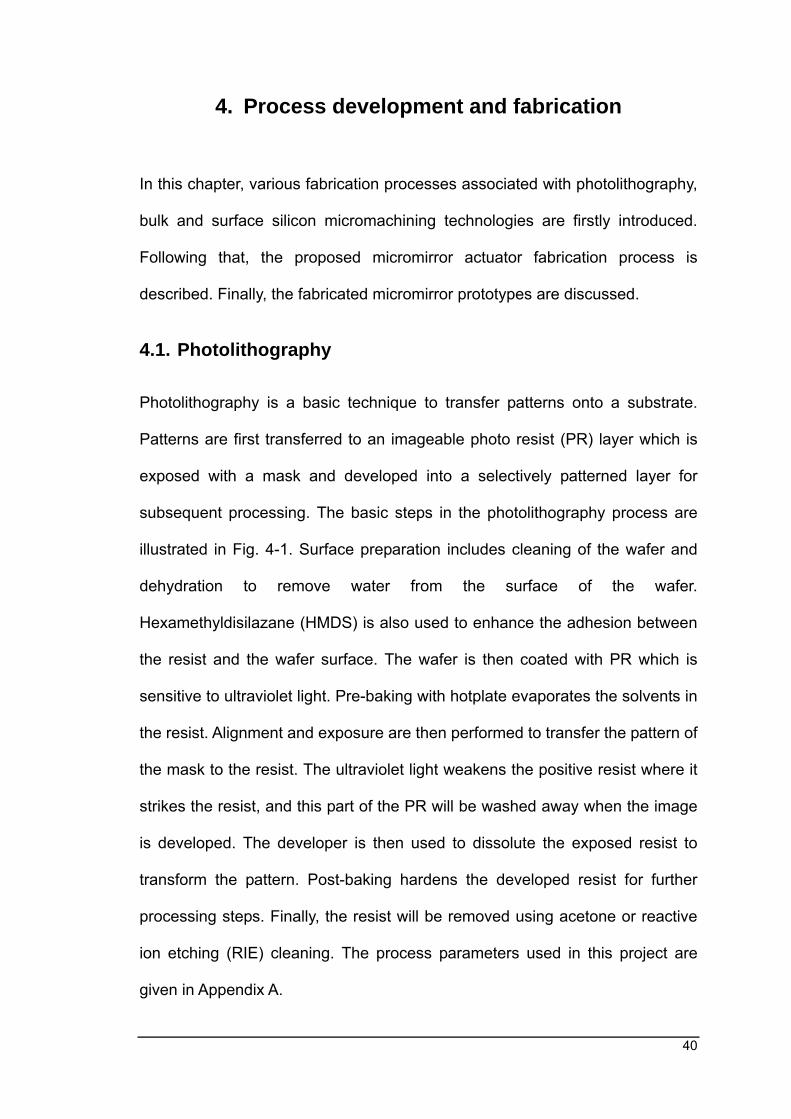
4.2.3. RIE
RIE (reactive ion etching) is one of the dry etching technologies. In RIE, the
substrate is placed inside a reactor in which several gases are introduced.
Plasma is struck in the gas mixture using a RF power source, breaking the gas
molecules into ions. The ions are accelerated towards and react at the surface
of the material being etched, which forms another gaseous material. This is
known as the chemical part of reactive ion etching. There is also a physical part
which is similar in nature to the sputtering deposition process. If the ions have
enough energy, they can knock atoms out of the material to be etched without a
chemical reaction. It is possible to influence the anisotropy of the etching by
changing the balance, since the chemical part is isotropic and the physical part
is highly anisotropic. The combination of the chemical and the physical parts
can form either rounded or vertical sidewalls. A schematic of a typical RIE
Pump
Heater
RF Signal
Gas Gas
Wafer
Shower Ring

Chapter 4 Process development and fabrication
44
system is shown in Fig. 4-4.
Fig. 4-4: Schematic of RIE system.
4.2.4. Sputtering
Sputtering is a technology in which the material is released from the source to
the substrate at low temperature. The substrate is placed in a vacuum chamber
with the source material, named a target, and an inert gas (such as argon) is
introduced at low pressure. A gas plasma is struck using an RF power source,
causing the gas to become ionized. The ions are accelerated towards the
surface of the target, causing atoms of the source material to break off from the
target in vapor form and condense on all surfaces including the substrate. A
schematic diagram of a typical RF sputtering system is shown in Fig. 4-5.
Wafer Plasma
Gas Gas
Insulator
Lower electrode Wafer holder
Pump
Diffuser Nossels
RF Signal
Upper electrode

Chapter 4 Process development and fabrication
45
Fig. 4-5: Schematic of RF sputtering system.
4.3. Bulk silicon micromachining
Bulk micromachining refers to the process in which three-dimensional features
are etched into the bulk of crystalline and noncrystalline materials [12]. Deep
reactive ion etching (DRIE) is a typical bulk silicon micromachining technology.
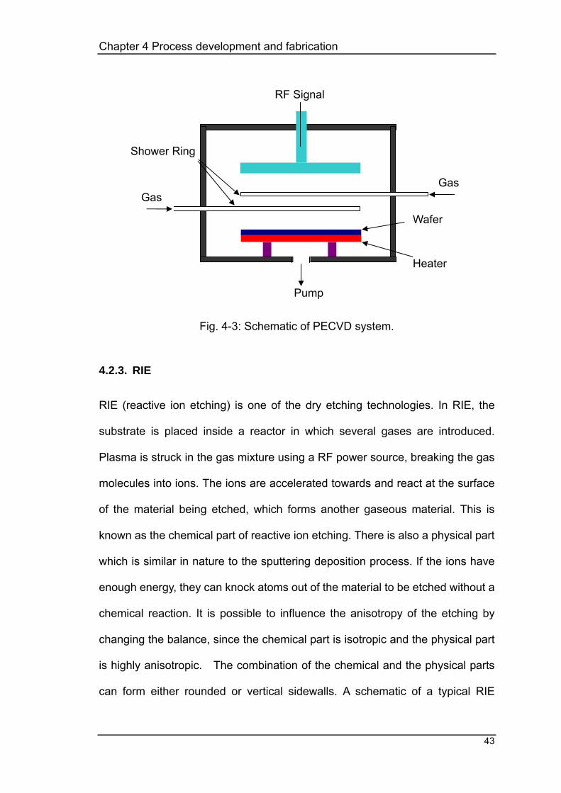
4.3.1. DRIE
DRIE is a special subclass of RIE which continues to grow rapidly in popularity.
In this process, etch depths of hundreds of microns can be achieved with
almost vertical sidewalls. The primary technology is based on the so-called
"Bosch process", named after the German company Robert Bosch which filed
the original patent. In Bosch process, two different gas compositions are
alternated in the reactor. The first gas composition creates a polymer on the
surface of the substrate, and the second gas composition etches the substrate.
The polymer is immediately sputtered away by the physical part of the etching,
but only on the horizontal surfaces and not the sidewalls. Since the polymer
Wafer
Vacuum pump inlet
RF SignalWatercooled sputter target
Plasma
Gas inlet
Counter electrode
Chapter 4 Process development and fabrication
46
only dissolves very slowly in the chemical part of the etching, it is built up on the
sidewalls and protects them from etching. As a result, etching aspect ratios of
50 to 1 can be achieved. The process can be easily used to etch through a
silicon substrate completely. The etch rate is 3-4 times higher than that of wet
etching. A schematic of STS DRIE etcher is illustrated in Fig. 4-6 [51].
Fig. 4-6: Schematic of DRIE system.
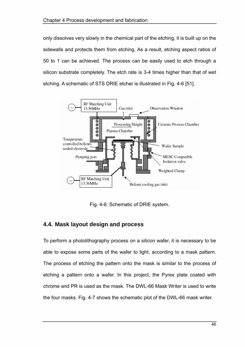
4.4. Mask layout design and process
To perform a photolithography process on a silicon wafer, it is necessary to be
able to expose some parts of the wafer to light, according to a mask pattern.
The process of etching the pattern onto the mask is similar to the process of
etching a pattern onto a wafer. In this project, the Pyrex plate coated with
chrome and PR is used as the mask. The DWL-66 Mask Writer is used to write
the four masks. Fig. 4-7 shows the schematic plot of the DWL-66 mask writer.

Chapter 4 Process development and fabrication
47
Fig. 4-7: The schematic plot of the DWL-66 Mask Writer.
4.4.1. Mask layout design
The first step is to use AutoCAD® to design the mask. In this project, four masks
are designed in one DXF file with different layers to ensure that these four
masks can be aligned well. The layer names should be capital so that the DXF
file can be transferred to CIF files by Coventor®.
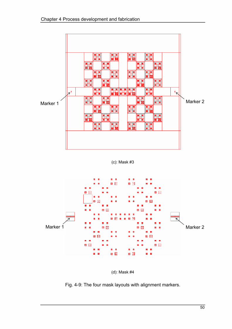
The four basic masks are plotted in Fig. 4-8. The four mask layouts for the
photolithographic steps in the process flow are shown in Fig. 4-9. Each has two
alignment markers at two sides.
Laser beam Filter
Shutter
Write-head
Mask
Optical crystal modulator
Granite base
Moving stage
Inferometer

Chapter 4 Process development and fabrication
48
Fig. 4-8: Four masks: (a) Mask #1 (Cantilever oxide layer pattern mask); (b) Mask #2 (Back side release mask); (c) Mask #3 (Cantilever pattern mask); (d)
Mask #4 (Mirror and electronical pads mask).
(a) Mask #1 (b) Mask #2
(c) Mask #3 (d) Mask #4

Chapter 4 Process development and fabrication
49
(a): Mask #1
(b): Mask #2
Marker 2Marker 1
Marker 2Marker 1
Chapter 4 Process development and fabrication
50
(c): Mask #3
(d): Mask #4
Fig. 4-9: The four mask layouts with alignment markers.
Marker 2Marker 1
Marker 2Marker 1

Chapter 4 Process development and fabrication
51
4.4.2. Mask process
The basic steps in writing a mask are outlined in Fig. 4-10. After the mask is
drawn, Coventor® is used to transfer DXF files to CIF files. Next, DWL-Convert
software is used to convert CIF files to LIC files which are the input files of the
current mask writer DWL-66. A few parameters are required to be set during
transfer. Write lens and exposure mode are the two most important parameters.
To simplify the mask drawing, different layers with different exposure modes are
designed and transferred. In this work, mask #1 and mask #2 are designed in
non-inverted mode, while mask #3 and mask #4 are designed in inverted mode.
After setting up the job parameters, the mask can be written by the mask writer.
Finally, the mask is obtained by developing the PR and etching the chrome
layer of the mask.
Fig. 4-10: The basic steps in writing a mask.
Create the mask design using AutoCAD®
Convert CIF files to LIC files
Set up the job parameters
Write the mask
Develop and post-bake
Chrome etch
Convert DXF files to CIF files using Coventor®
Copy files from the PC to the mask writer

Chapter 4 Process development and fabrication
52
4.5. Device fabrication
In this section, the process flow of the thermal actuated micromirror device is
proposed. To improve the device performance, the proposed fabrication
process is optimized, and the device prototypes are fabricated successfully.
4.5.1. Starting material
The starting wafer is a 425 µm thickness silicon-on-insulator (SOI) wafer with 2
µm thickness buried oxide layer and 2 µm thickness doping silicon device layer
shown in Fig. 4-11. The resistivity of the doping silicon layer is about 0.01
ohm-cm.
Fig. 4-11: Starting SOI wafer.
4.5.2. Process flow
1) Standard cleaning
The SOI wafers are first cleaned using the standard cleaning process
(Appendix B) as preparation for the subsequent thermal oxidation step.
2) Oxidation
Oxidation consists of three steps. First, 0.05 µm thickness oxide interface
layers are thermally grown at 1100 on both sides of SOI. Second, 1.3 µm
Silicon Silicon dioxide Doping silicon

Chapter 4 Process development and fabrication
53
bulk of oxide is deposited on the device layer by the PECVD oxide deposition at
300. Last, another 0.05 µm thickness oxide layers are thermally grown at
1100 on both sides of SOI. Though the quality of dry oxidation is superior,
the oxidation rate is too slow. Therefore, Dry oxidation steps (the first and the
last steps) are only used to form the interface layers; bulk of oxide mainly
comes from the PECVD oxide deposition. The topside oxidation layer is the top
layer of the bi-layer cantilever. The bottom side oxidation layer is the sacrificial
layer for backside release. The schematic result is shown in Fig. 4-12.
Fig. 4-12: Oxidation.
3) Topside oxide layer pattern
The schematic process flow of the topside oxide layer patterning is shown in
Fig. 4-13. HMDS and PR AZ 4620 are first coated on the topside as shown in
Fig. 4-13 (a). The PR is lithographically patterned by exposing it to UV light
through Mask #1 and developed. The PR in exposed areas is then removed
using AZ 400K developer, and leaving behind a patterned PR mask for etching
is as shown in Fig. 4-13 (b). Next, RIE is used to remove the unwanted oxide.
After the etching, the PR is chemically stripped in Acetone bath as shown in Fig.
4-13 (c).
Silicon Silicon dioxide Doping silicon

Chapter 4 Process development and fabrication
54
Fig. 4-13: Photolithographic patterning and RIE patterning.
4) Backside oxide layer pattern
The wafer is recoated with PR AZ4620 on the backside and lithographically
patterned using Mask #2. Backside alignment method is used during
photolithography. The unwanted oxide is removed using RIE and the PR is
stripped as shown in Fig. 4-14.
Fig. 4-14: Backside DRIE patterning.
5) Topside cantilevers and mirror pattern
Similarly, the wafer is recoated with PR AZ4620 on the topside and is
lithographically patterned with Mask #3. DRIE is used to etch the doping Si
layer for about 2 minutes as shown in Fig. 4-15. The etching process stops at
the buried oxide layer.
(a)
(b)
(c)
Silicon dioxide Doping silicon PR AZ 4620
Silicon
Silicon dioxide Doping silicon
Silicon

Chapter 4 Process development and fabrication
55
Fig. 4-15: Topside cantilevers and mirror substrate patterning.
6) Mirror, interconnect lines and pads patterns by Lift-off
The wafer is coated with LOR 30B (Fig. 4-16 (a)) and PR AZ 1512 (Fig. 4-16 (b))
on the topside and is lithographically patterned with Mask #4. AZ developer and
AZ 400 K developer are used sequentially to develop PR AZ 1512 (Fig. 4-16 (c))
and LOR 30B to create a bi-layer reentrant sidewall profile shown in Fig. 4-16
(d). Due to the equipment limitation, Tantalum/Copper (Ta/Cu) instead of Gold is
sputtered using sputtering system (Fig. 4-16 (e)). Ta is deposited to enhance
the adhesion between the copper layer and the wafer surface. PG remover is
used to remove unwanted Ta/Cu (Fig. 4-16 (f)). The SEM picture is shown in
Fig. 4-17.
Silicon dioxide Doping silicon
Silicon

Chapter 4 Process development and fabrication
56
Fig. 4-16: Mirror, interconnect lines and pads patterns Lift-off.
(c)
(d)
(e)
(f)
Silicon Oxide Doping silicon Ta/Cu LOR 30B AZ 1512
(c)
(a)
(b)

Chapter 4 Process development and fabrication
57
(a) (b)
Fig. 4-17: SEM pictures of topside view before backside release. (a) the top view of the whole structure. (b) the zoomed picture.
7) Backside release
PR is used to attach another handle wafer on the topside of SOI. DRIE is then
used to etch the backside silicon for about three hours. The etching stops at the
buried oxide layer. Follow that, the buried oxide layer is removed by RIE and
the topside PR is stripped in Acetone bath. Finally, the process for the actuated
micromirror is completed, as shown in Fig. 4-18.
Fig. 4-18: Backside release
Three hours DRIE is required to complete the backside release process. Long
time DRIE without PR protection leads to the destroyed hinge structures as
shown in Fig. 4-19. PR on the handle wafer is also burned during the long time
DRIE as shown in Fig. 4-20.
Silicon dioxide Doping silicon
SiliconTa/Cu
Ta/Cu Pad and interconnect line
Mirror
Bi-layer cantilever

Chapter 4 Process development and fabrication
58
Fig. 4-19: SEM picture of released structure with broken hinge.
Fig. 4-20: Surface roughness after resist burned.
Broken hinge

Chapter 4 Process development and fabrication
59
4.5.3. Process improvement
In order to improve the yield, the process flow is modified as follows: the
backside etching of 300 µm is done before the topside device patterning
processes. The protection PR is also coated on both the holder wafer and the
device layer, which shortens the time for DRIE. As a result, device structures
will not be destroyed. The topside PR for protection will not be burned either.
Glue instead of PR is used to bond the wafers, as it is much easier to debond.
The detailed process flow is shown in the following.
1) Standard cleaning
The SOI wafers are first cleaned using the standard cleaning process
(Appendix B) as preparation for the subsequent thermal oxidation step.
2) Oxidation
Oxidation consists of three steps. First, 0.05 µm thickness oxide layers are first
thermally grown at 1100 on both sides of SOI. Second, 1.3 µm bulk of oxide
is deposited on the device layer by the PECVD oxide deposition at 300. Last,
another 0.05 µm thickness oxide layers are thermally grown at 1100 on both
sides of SOI. The top side oxidation layer is the second layer of the bi-layer
cantilever. The bottom side oxidation layer is the sacrificial layer for backside
release as shown in Fig. 4-21.

Chapter 4 Process development and fabrication
60
Fig. 4-21: Oxidation.
3) Topside oxide layer pattern
HMDS and PR AZ 4620 is first coated on the topside, lithographically patterned
by exposing it to UV light through Mask #1, and then developed. RIE is used to
remove the unwanted oxide. After the etching, the PR is chemically stripped in
Acetone bath as shown in Fig. 4-22.
Fig. 4-22: Topside oxide pattern.
4) Backside DRIE etching
The wafer is recoated with PR on the backside and lithographically patterned
using Mask #2. Backside alignment is used during photolithography. The
unwanted oxide is removed using RIE. Backside DRIE etch for 2.5 hours with
etching rate 2.5 µm per minute. About 100 µm backside silicon layer is kept to
protect the topside structures. The PR is stripped as shown in Fig. 4-23.
Fig. 4-23: Backside DRIE nearly etching through.
Silicon dioxide Doping silicon PR AZ 4620
Silicon
Silicon dioxide Doping silicon PR AZ 4620
Silicon
SiliconSilicon dioxide Doping silicon

Chapter 4 Process development and fabrication
61
5) Topside cantilevers and mirror pattern
The wafer is recoated with PR AZ 1512 instead of PR AZ 4620 on the topside
and is lithographically patterned with Mask #3. This is because that PR AZ 1512
profile has no undercut while AZ 4620 profile has undercut. DRIE is used to
etch to the buried oxide layer from the topside for about 2 minutes as shown in
Fig. 4-24.
Fig. 4-24: Topside cantilevers and mirror substrate pattern.
6) Mirror, interconnect lines and pads patterns Lift-off
The wafer is coated with LOR 30B and PR AZ 1512 on the topside and is
lithographically patterned with Mask #4. AZ develop and AZ 400 K develop are
used sequentially to develop PR AZ 1512 and LOR 30B. Ta/Cu is then
sputtered using Sputtering system. Finally, PG remover is used to remove
unwanted copper as shown in Fig. 4-25.
Fig. 4-25: Mirror, interconnect lines and pads patterns Lift-off.
7) Backside release
The SOI wafer and the topside of the hold wafer are both coated with PR AZ
4620 for protection. DRIE is used to etch the backside silicon to release the
Silicon dioxide Doping silicon
SiliconTa/Cu
Silicon dioxide Doping silicon
Silicon

Chapter 4 Process development and fabrication
62
structures. Then the wafer is debonded and the topside PR and glue is stripped
in Acetone bath. Finally, the buried oxide layer is removed by RIE as shown in
Fig. 4-26. The process for the actuated micromirror is finally completed.
Fig. 4-26: Backside release.
Some of the device prototypes are given through Fig. 4-27 to Fig. 4-32. Figs.
4-27 and 4-28 show the Design 7 prototype. The cantilever oxide layer as
shown in Fig. 4-28 (b) looks brighter than other parts. It is because this isolator
layer concentrates more electrons during SEM imaging. The black spots
through Fig. 4-29 to Fig. 4-32 are PR remainders due to the undesirable
process control. Prototype of Design 8 is shown in Fig. 4-32, but many Design 8
prototypes are broken at the connection point of the hinge to the mirror plate
during the last release step. It is thought that the stress exerted on the
connection hinges by the initial bending of the cantilevers exceeds the yield
strength. Furthermore, these figures show that the initial surface of the
micromirror is not perfectly flat because of the non-uniform stress in the
micromirror.
Silicon dioxide Doping silicon
SiliconTa/Cu

Chapter 4 Process development and fabrication
63
(a)
(b)
Fig. 4-27: Prototype of Design 7.

Chapter 4 Process development and fabrication
64
(a) The overall device structure
(b) The cantilever and hinge structures
Fig. 4-28: SEM pictures of Design 7 after testing.
Hinge
Cantilever oxide layer

Chapter 4 Process development and fabrication
65
Fig. 4-29: SEM pictures of Design 1.
Fig. 4-30: Prototype of Design 2.

Chapter 4 Process development and fabrication
66
Fig. 4-31: Prototype of Design 6.
Fig. 4-32: Prototype of Design 8.

Chapter 4 Process development and fabrication
67
4.6. Summary
The fabrication process of the MEMS actuator integrated with micromirror is
developed and optimized. The prototypes are fabricated successfully. Moreover,
the surface of the device prototypes becomes much cleaner than the former
round prototypes after the process optimization. However, the initial surface of
the micromirror is not perfectly flat due to the non-uniform stress in the
micromirror. There are also some PR remainders on the surface of the devices.
The fabrication process needs to be improved for better fabrication yield and
cleaner devices.

69
5. Test and calibration
In this chapter, the cantilever resistance of the device prototype is characterized
using probe station and semiconductor characterization system. The static
displacement and frequency response of micromirror device are also measured
by Laser Doppler Vibrometer (LDV) to compare with the simulation results.
Finally, the piezoresistive sensing function is calibrated.
5.1. Resistance measurement
Resistance of the cantilevers is measured using RHM-06 Manual Hybrid Probe
Station and Semiconductor Characterization System 4200 as shown in Fig. 5-1.
Two probes are employed to add DC testing voltage on two pads of the thermal
actuators. To eliminate the resistance change caused by piezoresistive effect
and temperature change effect on the cantilevers, 0-1mV DC sweep is applied
using RHM-06 Manual Hybrid Probe Station to measure the pure resistance of
the device. Current and Voltage relation plot (I-V) is given by the Semiconductor
Characterization System in Fig. 5-2. It is observed from Fig. 5-2 that the
resistance of the two cantilevers in series is about 5.8kΩ. Then the resistivity of
of the doping silicon layer can be calculated with Equation (5.1). It is found that
the resistivity is around the design value of 0.01Ω-cm.
WLR Rρ= (5.1)
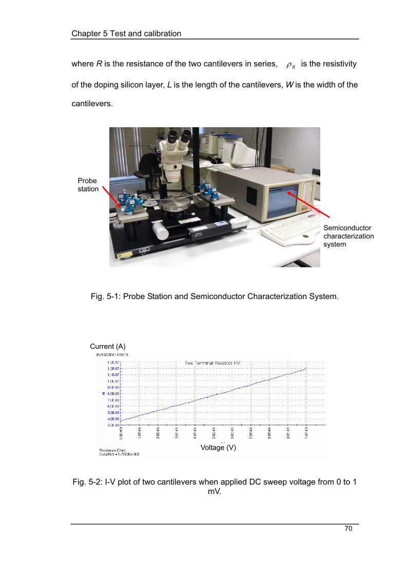
Chapter 5 Test and calibration
70
where R is the resistance of the two cantilevers in series, Rρ is the resistivity
of the doping silicon layer, L is the length of the cantilevers, W is the width of the
cantilevers.
Fig. 5-1: Probe Station and Semiconductor Characterization System.
Fig. 5-2: I-V plot of two cantilevers when applied DC sweep voltage from 0 to 1 mV.
Current (A)
Voltage (V)
Probe station
Semiconductor characterization system

Chapter 5 Test and calibration
71
5.2. MEMS mirror displacement measurement
To verify the device prototype performance, the micromirror actuator prototypes
are tested by a setup as shown in Fig. 5-3. The experimental platform is
illustrated in Fig. 5-4. The out-of-plane displacement of the micromirror actuator
under 3V, 0.5s square wave is measured by Laser Doppler Vibrometer (LDV).
Fig. 5-3: The test setup for the actuator.
Fig. 5-4: The test platform for the thermal actuator.
Oscilloscope
Laser Doppler Vibrometer CCD
Function Generator
Probe station
Device
Microscope
Microscope
PC
LDV
Probe station
Oscilloscope
Dynamic Signal Analyzer

Chapter 5 Test and calibration
72
Fig. 5-5 shows the experimental data from oscilloscope including the input
square wave and the output from the mirror movement with respect to time. The
measured displacement results are compared with the simulated results under
3V DC as shown in Fig. 5-6. There is a good match except for some deviations
between the measured and the simulated results. The major reason for this
variation is the contact resistance between the probe tip and the contact pad
during measurement which leads to the actual driving voltage smaller than the
readout of the power supply. Therefore, the measured displacement is smaller
than the simulated results. However, this problem could be improved by using
the wire bond instead of the probe tip during experimental measurement.
Moreover, the ignorance of the thermal conduction due to air and the variation
of material properties due to temperature change in the simulation model are
also possible error sources. This problem can be improved by including the air
effect and by considering the variation of material properties in the simulation
model.

Chapter 5 Test and calibration
73
Fig. 5-5: Experimental data from oscilloscope showing the input square wave and the output from the mirror deflection with respect to time.
1.8 2.0 2.2 2.4 2.6 2.8 3.0 3.2 3.4 3.6
0.4
0.6
0.8
1.0
1.2
1.4
Measurement Simulation
Voltage(V)
Dis
plac
emen
t(µm
)
Fig. 5-6: Deformation results of measurement and simulation.

Chapter 5 Test and calibration
74
5.3. Frequency response
The dynamic response of the micromirror actuator is also evaluated, and the
out-of-plane velocity of the actuator is measured by LDV. To avoid the effect of
the thermal characteristic of the actuator [29], a mini-shaker type 4810 is used
to conduct the vibration test as shown in Fig. 5-7. The measured frequency
response in Fig. 5-8 shows the dynamic characteristic of the micromirror
actuator prototype. Apparently, the first mechanical resonance frequency of the
device is at 7 kHz which is about 30% lower than the simulated values. This
deviation may be caused by the PR kept on the surface of the device which
reduces the resonance frequency due to the extra PR mass. Further FEM
modal analysis including the remained PR effect is performed for verification.
From the FEM results, it is found that the first resonance frequency is 8.6 kHz
which is closer to the testing result of 7 kHz. The deviation may be also caused
by the differences between the designed and fabricated device parameters in
processing techniques, and the neglected air damping effect as well as the
thermal losses.
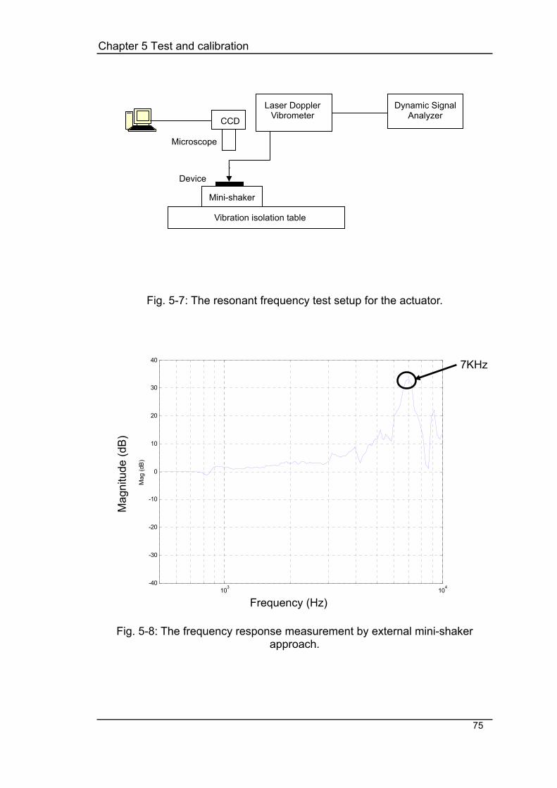
Chapter 5 Test and calibration
75
Fig. 5-7: The resonant frequency test setup for the actuator.
103
104
-40
-30
-20
-10
0
10
20
30
40
Mag
(dB
)
Fig. 5-8: The frequency response measurement by external mini-shaker approach.
Laser Doppler Vibrometer CCD
Mini-shaker
Device
Microscope
Dynamic Signal Analyzer
Vibration isolation table
Frequency (Hz)
Mag
nitu
de (d
B)
Frequency (Hz)
7KHz

Chapter 5 Test and calibration
76
5.4. Piezoresistive sensing function
In fact, doping silicon layer cantilever can be used as the piezoresistive sensor
element [52]. In each bi-layer cantilever of the micromirror actuator, 4×1019cm-3
boron-doped silicon layer with resistivity of about 0.01-0.001Ωcm is used not
only as a heat resource element but also as a piezoresistive sensor. Due to the
bimorph effect, the cantilever is able to drive the micromirror to move vertically
when applying voltage to the bi-layer cantilevers. In the meantime, the vertical
displacement of the micromirror could also be sensed by measuring the
resistance change of the doping silicon layer.
In order to verify this sensing function, a Wheatstone bridge circuit is used to
measure the resistance change of the two cantilevers in series. The constant of
the Wheatstone bridge circuit is calibrated as 10.46Ω/V. Then, 0.1 V voltage
source is applied to the Wheatstone bridge circuit when the micromirror is
forced down 1µm via a probe tip. Fig. 5-9 shows the measured voltage change.
The output voltage change is about 80mV. Therefore, the resistance change of
the two cantilevers in series is obtained as:
Ω=×Ω=∆ 8.080/46.10 mVVR
which can sense the out-of-plane displacement of the micromirror.

Chapter 5 Test and calibration
77
Fig. 5-9: The output voltage changing when the cantilever is brought down 1µm by the probe tip.
5.5. Summary
In order to verify the proposed device, the device prototypes are tested. Design
7 prototype is characterized in terms of resistance, mirror displacement,
frequency response and resistance change of the piezoresistive layers (doping
Si layers).
The resistivity of the doping silicon layer is about 0.04 KΩ-cm, which is around
the design value of 0.01 KΩ-cm. The micromirror can be actuated vertically to
1µm under 3V, 0.5s heating pulse. This test result is well compared with the
simulation results.

Chapter 5 Test and calibration
78
The frequency response of the device excited by a mini-shaker is detected by
LDV. The measured first mechanical resonance frequency of 7 kHz is about 30
% lower than the simulation result of 12.2 KHz. One main reason is that some
extra PR weight on the mirror surface reduces the resonance frequency. The
difference between the designed and fabricated mechanical parameters may
also cause the deviation. Moreover, neglecting air damping effect and the
thermal losses in simulation also affects the device testing results.
As a self-sensing actuator with micromirror, the displacement of the micromirror
could be detected by the resistance change of the cantilever piezoresistive
layers. The two cantilevers in series of the device have 0.8Ω resistance change
when the micromirror is forced down 1µm by probe tip.
In the future testing work, following work is recommended:
Apply 3V, 500 µs heating periodic pulse to the prototypes.
Compare the testing results with the transient simulation results
Test the reflectivity of the micromirror.
Measure the temperature of the prototypes during heating.

78
6. Conclusions
In this thesis, a novel thermal actuated micromirror is proposed as a
fine-tracking mechanism for optical disk drive. In the proposed device, the
bi-layer cantilevers consist of two materials with different thermal expansion
coefficients. Due to the bimorph effect, the micromirror suspended by four
identical bi-layer cantilevers alters the optical path of the incident laser beam
and linearly steers the focused laser beam spot on the optical media disk by its
out-of-plane translational movement.
Doping Si and Si dioxide are selected as two materials for the bi-layer
cantilevers. The thicknesses of doping Si and Si dioxide layers are designed by
the numerical analysis and optimization. The doping Si layer is not only a heat
source but also a piezoresistive sensor. Thus, the novel thermal actuator could
also sense the mirror movement.
The device performance is evaluated and optimized using FEM analyses in
eight design cases. Static deformation analysis is performed to evaluate the
residual stress induced deformation. Electrothermal and mechanical analyses
are carried out to calculate the temperature, stress and displacement
distributions of the micromirror actuator. In particular, for design7, the transient
analysis results show that the micromirror could be actuated vertically to 1µm
with 650 µs thermal time constant and maximum temperature 100 under only
3V, 500µs periodic pulse. Its maximum stress of 160MPa is located at the hinge

Chapter 6 Conclusion
79
and the first mechanical resonance frequency is 12.2 KHz.
The proposed thermal actuated micromirror has been fabricated successfully
by MEMS technology compatible to standard IC process. However, PR on the
top side of the devices is not stripped thoroughly. In addition, some device
prototypes such as Design 8 are broken. The fabrication process needs to be
further improved to obtain better fabrication results.
The calibration and test work is conducted to verify the characteristics of the
micromirror actuator prototypes. Displacement and frequency response are
measured with probe station and LDV. The experiment results show that the
micromirror can be actuated vertically to 1µm under 3 V 0.5s heating pulse. It is
compared well with the simulation results. The first resonance frequency is at
about 7 kHz, as compared with the designed result of 12.2 KHz. There are
some deviations between the measured and the simulated results. One main
reason is that some PR kept on the device surface reduces the frequency value.
The modified simulation result with PR remainder is 8.6 KHz. The difference
between the designed and the fabricated parameters may also cause the
deviation. Neglecting air damping effect and the thermal losses could also
result in the frequency response deviations.
The piezoresistive sensing function is verified by measuring the resistance
change of the cantilever piezoresistive layers. The testing results reveal that the
two cantilevers in series have 0.8Ω resistance change when the micromirror is

Chapter 6 Conclusion
80
moved down to 1 µm by the probe tip.
Recommendations for future works are as followings:
Doping silicon layer has the piezoresistive effect. Self-detected thermal
actuated micromirror can be realized with separated sensor part shown in
Fig. 6-1. The piezoresistive sensor at the fixed ends of the four cantilevers
could measure the micromirror deformation more sensitively.
More wafer lever devices are needed for a more precise testing and
calibration work.
The more precise testing method and dynamic testing work should be
performed to get accurate measurement results.
The residual stress induced deformation need be measured once the
device is released. Then, the initial residual stress in the oxide layer can be
obtained.
Fig. 6-1: The modified self-detected thermal actuated micromirror.
Doping Si piezoresistive sensor
Si dioxide & Doping Si bi-layer
til
Gold mirror
Silicon substrate
Gold Interconnect lines

81
References
[1] Freeman, P. D., K. Falta, L. Fan, S. Gloeckner and S. Patra. Digital MEMS
for Optical Switching, Communications Magazine, IEEE, Vol. 40, Issue 3,
pp. 88 – 95. Mar. 2002.
[2] Mechels, S., L. Muller, G.D. Morley and D. Tillett. 1D MEMS-based
wavelength switching subsystem. Communications Magazine, IEEE, Vol.
41, Issue 3, pp. 88 – 94. Mar. 2003.
[3] Watanabe, I., Y. Ikai, T. Kawabe, H. Kobayashi, S. Ueda and J. Ichihara.
Precise track-following control using a MEMS tracking mirror in
high-density optical disk drives. In Optical Memory and Optical Data
Storage Topical Meeting, 2002. International Symposium, on 7-11, pp.
257-259, Jul. 2002.
[4] Freeman, M.O. Miniature high-fidelity displays using a biaxial MEMS
scanning mirror (invited talk), Proc. SPIE 4985, pp. 56–62. 2003.
[5] Dickensheets, D.L. and G.S. Kino. Silicon-Micromachined Scanning
Confocal Optical Microscope, J. Microelectromech. Syst. 7 (1), pp. 38-47.
1998.
[6] Pan, Y. and H. Xie, G. Fedder. Endoscopic optical coherence tomography
based on a microelectromechanical mirror, Opt. Lett. 26 (24), pp.
1966-1968. 2001.
[7] Cornett, K.T., B. Walker, E.J. Carr and J.P. Heritage, O. Solgaard. Effects of
mirror surface deformation in optical delay lines based on
resonant-scanning micromirrors, In IEEE/LEOS Annual Meeting
Conference, 2, pp.855–856. 2001.

References
82
[8] Ryf, R. et al. 1296-port MEMS transparent optical crossconnect with 2.07
petabit/s switch capacity. In Proc. of the Technical Digest of Optical Fiber
Communication Conference, Anaheim, CA, USA, Post deadline paper
PD-28. March 2001.
[9] Hagelin, P.M., U. Krishnamoorthy, J.P. Heritage and O. Solgaard. Scalable
optical cross-connect switch using micromachined mirrors, IEEE Photonics
Technol. Lett. 12 (7), pp. 882–885. 2000.
[10] Yee, Y., H. –J. Nam, S. –H. Lee, J. U. Bu and J.-W. LEE. PZT actuated
micro mirror for fine-tracking mechanism of high-density optical data
storage. Sensors and Actuators A 89, pp. 166-173. 2001.
[11] Tai-Ran Hsu. MEMS & Microsystems Design and Manufacture. pp. 1-5,
Singapore: McGraw-Hill International Edition. 2002
[12] Madou, M. Fundamentals of Microfabrication. The 2nd edition, pp. 1-5
(Roadmap section), New York: CRC Press LLC. 2002.
[13] Pisano, A. In presentation material distributed by the United States Defense
Advanced Research Program Agency (DARPA), available at
http://web-ext2.darpa.mil.
[14] Bratter, R. L. Commercial Success in the MEMS Marketplace, Optical
MEMS, 2000 IEEE/LEOS International Conference on, pp. 29-30. Aug.
2000.
[15] Payne, R.S., S. Sherman, S. Lewis, and R.T. Howe (Edited by: Wuorinen,
J.H.). Surface micromachining: from vision to reality to vision
(accelerometer). In Proc. ISSCC '95-International Solid-State Circuits
Conference, pp. 164-165. 1995.

References
83
[16] Senturia, Stephen D. Microsystem Design, pp. 531-536, Boston: Kluwer
Academic Publishers. 2001
[17] Kessel, P. F., L. J. Hornbeck, R. E. Meier, and M. R. Douglass. A
MEMS-based projection display. In Proc. IEEE, Vol. 98, pp. 1687-1704.
1998.
[18] Solgaard, O., F. S. A. Sandejas, and D. M. Bloom. Deformable grating
optical modulator, Opt. Lett. Vol. 17, pp. 688-690. 1992.
[19] Jahja I. Trisnadi, Clinton B. Carlisle and Robert Monteverde. Overview and
applications of Grating Light ValveTM based optical write engines for
high-speed digital imaging. In Photonics West 2004 - Micromachining and
Microfabrication Symposium, San Jose, CA, USA. Jan. 26, 2004.
[20] Bratter, R. L. Commercial Success in the MEMS Marketplace. In Optical
MEMS, 2000 IEEE/LEOS International Conference, pp. 29-30. Aug. 2000.
[21] Huber, J. E. Ferroelectrics: models and applications. Ph. D thesis,
University of Cambridge. 1998.
[22] Ishihara, H. and F. Arai. Micro Mechatronics and Micro Actuator,
IEEE/ASME Transactions on Mechatronics, Vol. 1, No. 1. Mar. 1996.
[23] Tang, W. C., T. –C. H. Nguyen and R. T. Howe. Laterally driven polysilicon
resonant microstructures, Sensors and Actuators, Vol. A20, pp. 25-32.
1989.
[24] Mehregany, M., P. Nagarkar, S. D. Sentura and J. H. Lang. Operation of
microfabricated harmonic and ordinary side-drive motors. Proc. IEEE
MEMS, pp. 1-8. 1990.
[25] http://www.sfu.ca/immr/gallery/.

References
84
[26] http://tima.imag.fr/mns/mcs/app/mumps/motor.html.
[27] Varadan, V. K., Xiaoning. Jiang and V. V. Varadan, Microstereolithography
and other fabrication technologies for 3D MEMS. Chichester: John Wiley
and Sons. Ltd. 2001.
[28] Kolesar, E.S., Jr., S.Y. Ko, J.T. Howard, P.B. Allen, J.M. Wilken, N.C.
Boydston, M.D. Ruff and R.J. Wilks. Thermally-Actuated Cantilever Beam
for Achieving Large In-Plane Mechanical Deflections, Thin Solid Films, Vol.
335-336, No. 1-2, pp. 295-302. 1999.
[29] Wen-Chih C., Chien-Cheng C, Jerwei H., Wieleun F. A reliable single-layer
out-of-plane micromachined thermal actuator, Sensors and Actuators A,
103, pp. 48-58. 2003.
[30] M.A.H. van der Aa, M.A.J. van As, A.L. Braun, B.H.W. Hendriks, C.T.H.
Liedenbaum, B. van Rompaey, G.E. van Rosmalen, J.J.H.B. Schleipen, H.J.
Borg, G.J.P. Nijsse, P.G. Nuijens, N.P.D.M. van Aken, P.T. Jutte, J.M.G.
Renckens, R.I. van Steen, S. Bramwell, P. Stavely, Small Form Factor
Optical Drive: Miniaturized Plastic High-NA Objective and Optical Drive,
Proc. ISOM/ODS, pp. 251–253. 2002.
[31] Sadik C. Esener, Mark H. Kryder, William D. Doyle, Marvin Keshner, Masud
Mansuripur and David A. Thompson. WTEC Panel Report on The Future of
Data Storage Technologies. Jun. 1999.
[32] Kim, S. –H., Y. Yee, J. Choi, H. Kwon, M. –H. Ha, C. Oh, J. U. Bu. A micro
optical flying head for a PCMCIA-sized optical data storage. In Proc. of
MEMS, 2004, pp. 85-88. Jan. 2004.
References
85
[33] Mansuripur, M., G. Sincerbox. Principle and Techniques of Optical Data
Storage, Proc. of THE IEEE, Vol. 85, NO. 11. Nov. 1997.
[34] Hirano, T., L.-S. Fan, T. Semba, W. Y. Lee and J. Hong. Micro-actuator for
tera-storage. In Proc. of MEMS’99, Orlando, FL, pp. 441-446. Jan. 1999.
[35] Minh, P. N., T. Ono and M. Esashi. A novel fabrication method of the tiny
aperture tip on silicon cantilever for near field scanning optical microscopy.
In Proc. of MEMS’99, Orlando, FL, pp. 360-365. Jan. 1999.
[36] Ghislain, L. P., V. B. Elings, K. B. Crozier, S. R. Manalis, S. C. Minne, K.
Wilder, F. S. Kino and C. F. Quate. Near-filed photolithography with a solid
immersion lens. Appl. Phys. Lett. 74 (4), pp. 501-503. 1999.
[37] Kino, G. S. Optical background for near-field recording. In Proc. of Magneto
Optical Recoding International Symposium, Monterey, CA, pp. 1-6. Jan.
1999.
[38] Sumi, S., A. Takahashi, T. Watanabe. Advanced storage magnetooptical
disk (AS-MO) system. In Proc. of Magneto Optical Recoding International
Symposium, Monterey, CA, pp. 173-176. Jan. 1999.
[39] Horsley, D. A., A. Singh, A. P. Pisano, R. Horowitz. Angular micropositioner
for disk drives. In Proc. of MEMS’97, Nagoya, Japan, pp. 454-459. Jan.
1997.
[40] Hidenori I., A. Fumihito and F. Toshio. Micro mechatronics and micro
actuators. IEEE/ASME Transactions on Mechatronics, Vol. 1, No. 1, Mar.
1996.
[41] Riethmüller, W. and W. Benecke. Thermal excited silicon microactuators,
IEEE Trans. Elec. Dev. Vol. 35, No. 6, pp. 758-763. Jun. 1988.

References
86
[42] Timoshenko, S. Analysis of bimetal thermostats. J. Opt. Soc. Amer., Vol. 11,
pp. 233. 1925.
[43] Funk, J., J. Bühler, J. G. Korvink, H. Baltes. Thermomechanical modeling of
an actuated mirror, Sensors and Actuators, A 46-47, pp. 632-636. 1995.
[44] Liew, L.-A., A. Tuantranout, V. M. Bright. Modeling of thermal actuation in a
bulk-micromachined CMOS micromirror, Microelectronics Journal 31, pp.
791-801. 2000.
[45] Hal Jerman. Electrically-activated, normally-closed diaphragm valves, J.
Micromech. Microeng. 4, pp. 210-216. 1994.
[46] Buser, R. A., N.F. de Rooij, H. Tischhauser, A. Dommann and G. Staufert.
Biaxial scanning mirror activated by bimorph structures for medical
applications, Sensors and Actuators A, 31, pp. 29-34. 1992.
[47] Chu, W- H., M. Mehregany and R. L. Mullen. Analysis of tip deflection and
force of a bimetallic cantilever microactuator, J. Micromech. Microeng, 3,
pp. 4-7. Mar. 1993.
[48] Zienkiewicz, O. C. The Finite Element Method. The 3rd edition, pp. 1-5,
McGraw-Hill. 1977.
[49] ANSYS 7.0 documentation, ANSYS®, Inc.,2002.
[50] Xin Z, K-S Chen and S. M Spearing. Thermo-mechanical behavior of thick
PECVD oxide films. Sensors and Actuators A 103, pp. 263-270. 2003.
[51] Docker, P. T., P Kinnell and M C L Ward. A dry single-step process for the
manufacture of released MEMS structures, J. Micromech. Microeng., Vol
13, pp. 790–794. 2003.

References
87
[52] Harley, J. A. and T. W. Kenny. High-sensitivity piezoresistive cantilevers
under 1000 Å thick, Appl. Phys. Lett. 75 (2), pp 289-291. 1999.

88
Appendix A
Thermal actuated micromirror fabrication process flow
Starting materials: 425 µm thick silicon-on-insulator (SOI) wafer with 2 µm thick doping silicon device layer and 2 µm thick buried oxide layer.
Table A-1: Fabrication process flow of the MEMS actuator.
Step no. Stage Product Time
(minute) Comments
1 Wafer preparation RCA Cleaning See Appendix B
2 Dry thermal oxidation
Si oxide deposition on
both sides 30 About 0.05 µm
3 PECVD Oxide
deposition on topside layer
30 About 1.4 µm
4 Dry thermal oxidation
Si oxide deposition on
both sides 30 About 0.05 µm
HMDS coating, 3000rpm 0.5 Adhesion promoter
AZ4620 Coating, 3000rpm
0.5 Imaging resist, about 3 µm
Prebake, 100°C 1.5 hotplate
Exposure AZ420,soft
contact 1
Expose Dose = 28 (3.5x8) mJ/cm2(EVG620 Aligner, 350W lamp ) g-line (435
nm) AZ400K
development (1:4)
2.7 Developing Imaging PR
AZ4620, DI rinse, N2 blow dry
5 Lithography
Post-bake, 100°C 2 hotplate
6 RIE Oxide1 recipe 29 Judging by the color 7 RIE Clean recipe 15

Appendix A
89
Step no. Stage Product Time
(minute) Comments
HMDS Coating,3000rmp 0.5 Promoting adhesion of
the resist AZ4620 Coating,
3000rpm 0.5 Imaging resist, about 6 µm
Prebake, 100°C 1.5 hotplate
Backside Exposure
AZ4620,soft contact
1
Expose Dose = 28 (3.5x8) mJ/cm2(EVG620
Aligner, 350W lamp ) g-line (435 nm)
AZ400k development
(1:4) 2.5
Developing Imaging PR AZ4620, DIW rinse, N2
blow dry
8 Lithography
Post bake, 120°C 2 hotplate
9 RIE Oxide 1 recipe 5 Judging by the color
10 ICP Anisotropic etch 150 Forming beam and
mirror structures, judging by the color
11 RIE Clean recipe 15 Removal of resist AZ1512 Coating,
3000rpm 0.5 Imaging resist, about 3 µm
Pre bake, 100°C 1.5 hotplate
Exposure AZ,soft contact 0.25
Expose Dose = 28 (3.5x8) mJ/cm2(EVG620
Aligner, 350W lamp ) g-line (435 nm)
AZ development (1:1) 2
Developing Imaging PR AZ1512, DIW rinse, N2
blow dry
12
Lithography
Post bake, 120°C 2 hotplate
13 ICP Anisotropic, 2 µm /mins 5 Nearly Etching through
the back side 14 RIE Oxide1 recipe 15 Judging by the color
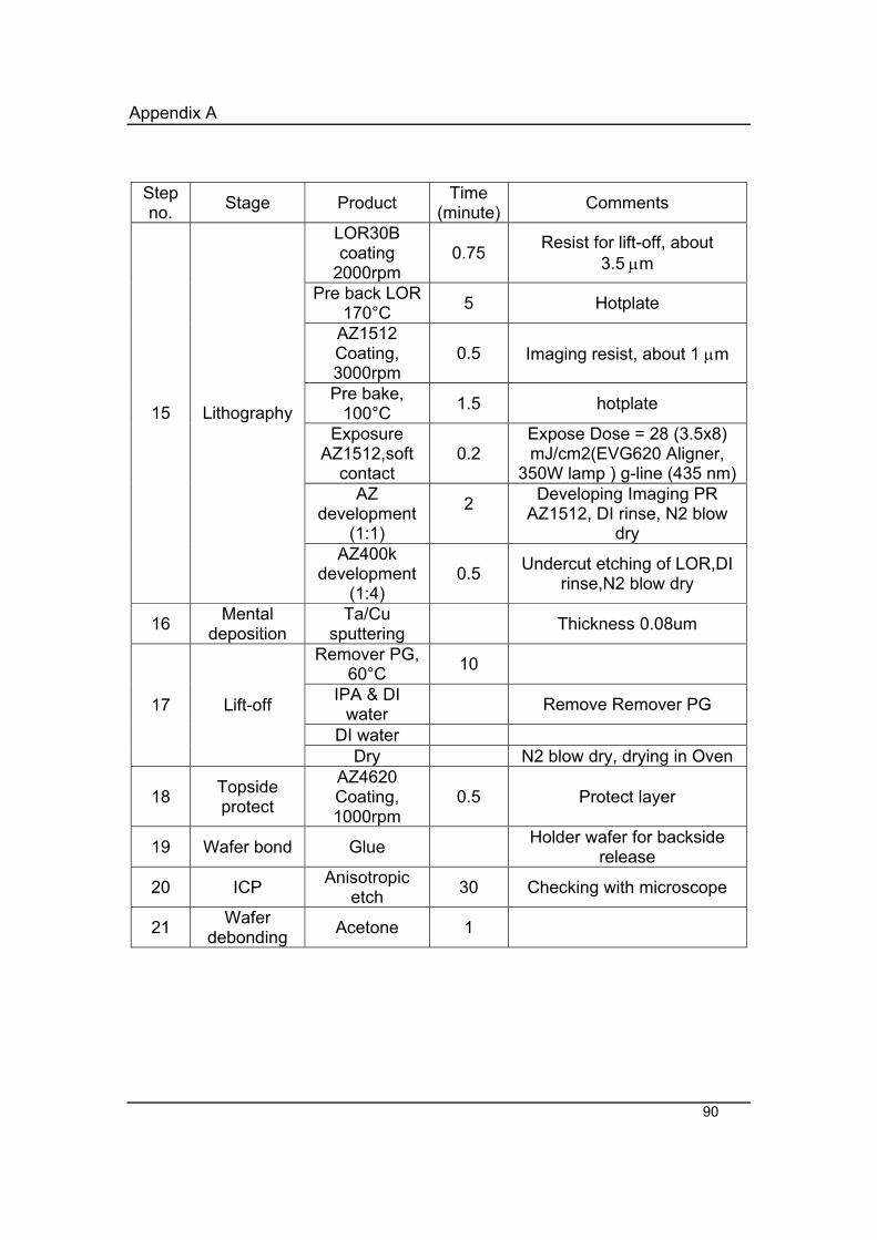
Appendix A
90
Step no. Stage Product Time
(minute) Comments
LOR30B coating
2000rpm 0.75 Resist for lift-off, about
3.5 µm
Pre back LOR 170°C 5 Hotplate
AZ1512 Coating, 3000rpm
0.5 Imaging resist, about 1 µm
Pre bake, 100°C 1.5 hotplate
Exposure AZ1512,soft
contact 0.2
Expose Dose = 28 (3.5x8) mJ/cm2(EVG620 Aligner,
350W lamp ) g-line (435 nm)AZ
development (1:1)
2
Developing Imaging PR AZ1512, DI rinse, N2 blow
dry
15 Lithography
AZ400k development
(1:4) 0.5 Undercut etching of LOR,DI
rinse,N2 blow dry
16 Mental deposition
Ta/Cu sputtering Thickness 0.08um
Remover PG, 60°C 10
IPA & DI water Remove Remover PG
DI water
17 Lift-off
Dry N2 blow dry, drying in Oven
18 Topside protect
AZ4620 Coating, 1000rpm
0.5 Protect layer
19 Wafer bond Glue Holder wafer for backside release
20 ICP Anisotropic etch 30 Checking with microscope
21 Wafer debonding Acetone 1

Appendix A
91
Step no. Stage Product Time
(minute) Comments
Acetone Ultrasonic
clean 3
IPA Ultrasonic clean 3
DIW rinse 6 cycles
22 Wafer clean
N2 dry
23 RIE Dioxide remover,30pw 30 Checking the color
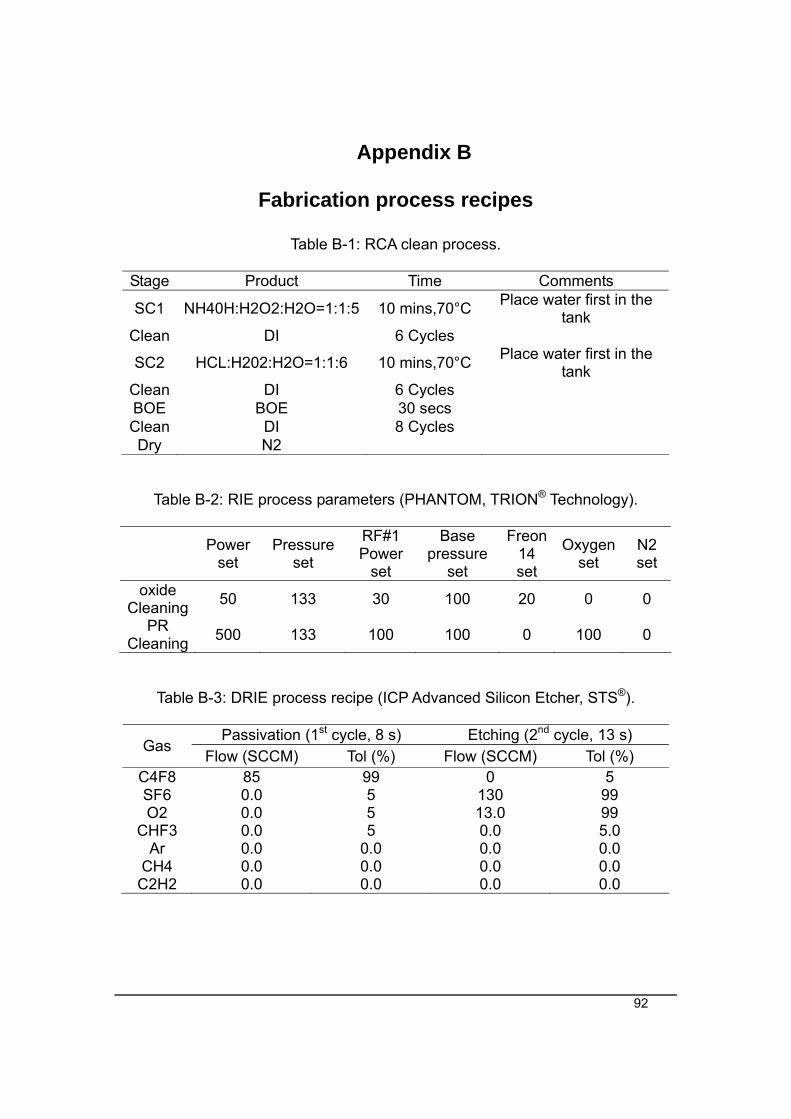
92
Appendix B
Fabrication process recipes
Table B-1: RCA clean process.
Stage Product Time Comments
SC1 NH40H:H2O2:H2O=1:1:5 10 mins,70°C Place water first in the tank
Clean DI 6 Cycles
SC2 HCL:H202:H2O=1:1:6 10 mins,70°C Place water first in the tank
Clean DI 6 Cycles BOE BOE 30 secs Clean DI 8 Cycles Dry N2
Table B-2: RIE process parameters (PHANTOM, TRION® Technology).
Power set
Pressure set
RF#1 Power
set
Base pressure
set
Freon 14 set
Oxygen set
N2 set
oxide Cleaning 50 133 30 100 20 0 0
PR Cleaning 500 133 100 100 0 100 0
Table B-3: DRIE process recipe (ICP Advanced Silicon Etcher, STS®).
Passivation (1st cycle, 8 s) Etching (2nd cycle, 13 s) Gas
Flow (SCCM) Tol (%) Flow (SCCM) Tol (%) C4F8 85 99 0 5 SF6 0.0 5 130 99 O2 0.0 5 13.0 99
CHF3 0.0 5 0.0 5.0 Ar 0.0 0.0 0.0 0.0
CH4 0.0 0.0 0.0 0.0 C2H2 0.0 0.0 0.0 0.0

Appendix B
93
Table B-4: PEVCD for SiO2 300 process recipe (Plasmalab 80 Plus, OXFORD®
INSTRUMENTS,).
Step Time (minute) Flow (SCCM) Pressure (Torr)
Forward power (W)
Temp stablisation 30
N2 flow 8 420 7.5e-6 0 N2 plasma 10 420 7.5e-9 20
N2 161 N20 710 SiO2 300 30 SiH4 9
7.5e-9 20