design methodology for modeling a microcontroller …
TRANSCRIPT
DESIGN METHODOLOGY FOR MODELING A MICROCONTROLLER
A Thesis Presented to
The Faculty of the
Fritz J. and Dolores H. RussCollege of Engineering and Technology
Ohio University
In Partial Fulfillment
of the Requirement for the Degree
Master of Science
by
Phillip D. Southard
June, 2000
THIS THESIS ENTITLED
“DESIGN METHODOLOGY FOR MODELING A MICROCONTROLLER”
by Phillip D. Southard
has been approved
for the School of Electrical Engineering and Computer Science
and the Russ College of Engineering and Technology
______________________________________________________________________Janusz Starzyk, Professor
School of Electrical Engineering and Computer Science
_______________________________________________________________________Warren K. Wray, Dean
Fritz J. and Dolores H. RussRuss College of Engineering and Technology

iii
ACKNOWLEDGMENTS
I would like to sincerely thank my father Dave, my mother Kris, my brothers Erik
and Andrew, my sisters Angela and Malissa, and my friends for their support during my
research. I would also like to thank Dr. Starzyk for his guidance and support. I also
thank the Sarnoff Corporation and the U.S. government for sponsoring my research.

iv
TABLE OF CONTENTS
ACKNOWLEDGMENTS ............................................................................................. iii
TABLE OF CONTENTS................................................................................................iv
LIST OF TABLES ..........................................................................................................vi
LIST OF FIGURES .......................................................................................................vii
SYMBOLS AND ABBREVIATIONS...........................................................................ix
1.0 INTRODUCTION......................................................................................................1
2.0 VHDL Modeling .........................................................................................................4
3.0 Intel 8031 Architecture ..............................................................................................7
3.1 Intel 8031 Addressing Modes and Instruction Set Notes .......................................123.2 Machine Cycle Sequence .......................................................................................143.3 Modeled Architecture.............................................................................................17
4.0 Brainstorming the Design, The Creative Process..................................................20
5.0 Testing and Verification ..........................................................................................28
6.0 Behavioral Model and Simulation Results.............................................................33
7.0 IS Model and Simulation Results............................................................................38
7.1 IS Model Simulation Results with Behavioral Code .............................................407.2 IS Model Simulation Results with R0 Test Code ..................................................43
8.0 Summary and Future Work....................................................................................46
References .......................................................................................................................47
Appendix A - Intel 8031 INSTRUCTION SET ...........................................................48

v
Appendix B - Instruction Set Model Test Code...........................................................56
Appendix C - Instruction Set Model Simulation Results with Test Code.................59
Appendix D - Machine Cycle VHDL Code Example ..................................................79
Appendix E - Decoder Process VHDL Example Code................................................91
Appendix F - ALU_OP Procedure Example Code......................................................96

vi
LIST OF TABLES
Table 1. Special Function Registers................................................................................9
Table 2. Modeled Register 0 Instructions ...................................................................17
Table 3. Essential Modeled Instructions .....................................................................18
Table 4. IS Model Instructions.....................................................................................18
Table 5. Register Addressing Mode Addition Instruction Set Subset......................21
Table 6. Register Transfer Table ..................................................................................23
Table 7. T Cycles and RTN for ADD,Rn .....................................................................38

vii
LIST OF FIGURES
Fig. 1. Block Diagram, Intel 8031 Core ..........................................................................7
Fig. 2. Intel 8031 Detailed Architecture .........................................................................8
Fig. 3. 256 Byte Ram Block............................................................................................10
Fig. 4. Lower Half of RAM Block .................................................................................11
Fig. 5. External Program Memory Fetches ..................................................................14
Fig. 6. Instruction Examples with State Timing ..........................................................15
Fig. 7. Intel 8031 Minimum System ..............................................................................16
Fig. 8. Simple State Diagram .........................................................................................24
Fig. 9. Test Bench Environment...................................................................................30
Fig. 10. Test Code ...........................................................................................................33
Fig. 11. Behavioral Simulation Chart 1.......................................................................34
Fig. 12. Test Code ...........................................................................................................35
Fig. 14. Test Code ...........................................................................................................36
Fig. 15. Behavioral Simulation Chart 3........................................................................37
Fig. 16. IS Model Simulation Chart 1...........................................................................40
Fig. 17. Test Code ...........................................................................................................41
Fig. 18. IS Model Simulation Chart 2..........................................................................41
Fig. 19. Test Code ..........................................................................................................42
Fig. 20. IS Model Simulation Chart 3...........................................................................42
Fig. 21. IS Model Simulation Chart 4...........................................................................43

viii
Fig. 22. IS Model Simulation Chart 5...........................................................................45

ix
SYMBOLS AND ABBREVIATIONS
ALE Address Latch Enable
ASIC Application-Specific Integrated Circuit
CAD Computer Aided Drafting
CMOS Complimentary Metal Oxide Semiconductor
DARPA Defense Advanced Research Projects Agency
FPGA Field Programmable Gate Array
IEEE Institute of Electrical and Electronics Engineers
IC Integrated Circuit
IS Instruction Set
LSB Least Significant Bit
MSB Most Significant Bit
PC Program Counter
PSENn Program Store Enable active low
RAM Random Access Memory
ROM Read Only Memory
RASSP Rapid-Prototyping Application Specific Signal Processors
RTL Register Transfer Level
RTN Register Transfer Notation
SFR Special Function Register
UUT Unit Under Test

x
VHDL VHSIC hardware description language
VHSICVery High Speed Integrated Circuit
1
1.0 INTRODUCTION
In the ever-changing world of technology, new ideas are born and legacy
technologies are left aside to be chronicled in the history books. Although new
technologies become available, sometimes it is necessary to maintain older technology
when servicing electrical systems. The U.S. military and other military units around the
world fight an ongoing battle against technology life cycles. Program managers of radar
systems or fire control systems may or may not redesign a unit due to the advent of new
technology. The lack of money usually prevents the redesign of systems. Since some
systems cannot be replaced using new technology, technicians are challenged to maintain
electrical systems with parts that are not procurable by commercial buyers and or
government purchasers.
The work described within this thesis presents an engineering solution that stems
from the problem of parts obsolescence as it pertains to military systems. Sarnoff
Corporation of Princeton NJ, has developed BiCMOS gate arrays that makes it possible
to emulate older technology with newer and faster technology, providing a pin for pin
replacement part. For this thesis, the Intel 8031 microcontroller was chosen as a device
that would be modeled with VHDL so that a military grade device would be available if
need be in the future to help maintain electrical systems used by the U.S. military.
The design methodologies used to develop a Behavioral and Instruction Set (IS)
model for the Intel 8031 and the results of testing these models will be presented. Very
High Speed Integrated Circuits Hardware Description Language (VHDL) was used to

2
create the Behavioral model and the IS model for the Intel 8031 microcontroller. VHDL
is a text based language that can capture the functionality of a digital device as simple as
a NAND gate to an advanced digital communications system. The nature of this
research project does not allow for disclosure of intellectual property, hence the actual
VHDL text files will not be provided. Certain aspects of the VHDL code developed will
be explained as needed. To verify the Behavioral and IS model of the Intel 8031, it was
decided that a Hardware Modeler from Synopsys would be used.
This thesis was sponsored in part by the Sarnoff Corporation and the U.S.
government. It is the intent of this research to develop a model for the Intel 8031
microcontroller. This will allow for an understanding of how to best replace obsolete
parts with new components, especially complex parts. The replacement of obsolete or
singled sourced parts by emulation of the existing chip or using remaining die at chip
supply houses usually yields a cost effective solution for the government and the tax
payer. Sometimes board or system redesigns are necessary to eliminate a high
percentage of system or board level obsolete components. This is often very expensive
and time consuming.
This thesis has been organized as follows. In chapter 2, a brief description of
VHDL and the associated levels of modeling are given. In chapter 3, an architecture
overview of the Intel 8031 is provided. Next, in chapter 4, an approach to modeling
microcontrollers and similar devices is described. The methods of testing and verifying
the models developed for this thesis are given in chapter 5. Chapters 6 and 7 discuss the

3
simulation results of the Behavior and the IS model respectively. Finally, conclusions
and recommendations for continuance of this research are discussed in chapter 8.

4
2.0 VHDL Modeling
The state-of-the-art of digital circuit design now provides for an efficient, CAD
oriented methodology for implementing digital designs, by using VHDL. In the not so
distant past, design engineers were forced to develop logic functions using Karnaugh
maps putting together their designs logic gate by logic gate.
During the 60’s and the 70’s system level and microcomputer design entailed
building systems out of many individual logic gates manufactured on Integrated Circuits
(IC). This design technique was very costly and time consuming. As the technology
moved forward from medium-scale integration (MSI) to large-scale integration (LSI), to
very large-scale integration (VLSI), the need for new design tools became apparent.
With the ability to incorporate many functions on one IC, engineers needed a way to
quickly design a function and or circuit and test the design. The standard known as
VHDL, was first created in 1987, [2]. VHDL allows for hardware description in a text-
based language. VHDL is similar to Ada, a government standardized, portable, and
object oriented software language. VHDL allows a design to model a digital system at
many levels of abstraction. A description can be as simple as a 2-input logic circuit or
an entire digital system.
As devised by the DARPA/TRI-Service Rapid-prototyping of Application
Specific Signal Processors (RASSP) and some aerospace contractors, there exists
taxonomy for VHDL models [6]. There are five different levels of modeling:

5
Performance modeling, Behavioral modeling, Instruction Set modeling, Register
Transfer Level (RTL) modeling, and Gate-Level modeling.
Performance modeling is used to specify the general make up of a complete
system. Items that might be specified in performance modeling could include frames per
second for a video processor or number of instructions per second for a processor.
Behavioral modeling adds one level of detail. A Behavioral model will include a
break down of the system into subcomponents and functional blocks. There is little
detail to how the functions will be physically implemented.
The next level of detail is included in the Instruction Set model. This level of
detail provides a model that can be used to simulate the instruction set of the
microcontroller, microprocessor, or DSP chip in question. This thesis focuses on the
instruction set model level.
RTL modeling is a level of detail that specifies exactly how data will transfer
from register to register. RTL is the most useful level of modeling to a designer who is
going to actually implement his or her design in an Application-Specific Integrated
Circuit (ASIC) or a Field Programmable Gate Array (FGPA). There are many synthesis
tools that will “synthesize” or translate the RTL model into a netlist of primitive
technology cells for placement and routing. There has been a great deal of focus in the
area of synthesis since this is where the designer can save many hours of work. Instead
of drawing thousands upon thousands of gates in a schematic, the VHDL savvy designer
can describe a design in a text-based language that can be automatically transferred to a
schematic in a matter of seconds.

6
The final level of detail is the Gate-Level model. After synthesis is complete, the
result is a netlist of primitive gates like NAND gates and NOR gates. This netlist can be
simulated with timing information provided by the vendor of the target silicon. This
simulation is called post synthesis pre place and route simulation.
As mentioned above, this thesis focuses on an IS model for the Intel 8031
microcontroller. Prior to developing a detailed IS model, a designer needs to understand
the two levels above an IS model, the Performance model and the Behavioral model. In
this case, the circuit of discussion has been thoroughly described in the datasheets
available from Intel. This documentation takes the place of the Performance model.
That leaves the Behavioral model to develop first.
The Behavioral model developed is an abstract model of the Intel 8031 that
demonstrates a basic understanding of how instructions are fetched and executed. The
model was written to give a starting point of understanding to the overall design. Hence
the Behavioral model will not have any physical implications pertaining to the original
microcontroller.
Once the Behavioral model has been written one can then focus on developing an
IS model. The IS model developed for this thesis allows for exercising a subset of Intel
MCS-51 instructions. Since the Intel 8031 is a feature-reduced version of the Intel 8051,
the Intel 8031 uses the MCS-51 instructions.

7
3.0 Intel 8031 Architecture
It is not the intent of this chapter to provide a thorough analysis of the Intel 8031
architecture. Fig. 1 provides a general overview of the Intel 8031. A sufficient portion
of the architecture will be described to give the reader an understanding of the Intel 8031
as it relates to the research presented.
Intel 8031 core features [5]:
• 8 bit CPU optimized for Control Applications• Extensive Boolean processing (single-bit logic) capabilities• 64K Program Memory address space• 64K Date Memory address space• 128 bytes of on-chip Data RAM• 32 bi-directional and individually addressable I/O lines• Two 16-bit timer/counters• Full duplex UART• 6-source/5-vector interrupt structure with two priority levels• On-chip clock oscillator
EXTERNAL
Fig. 1. Block Diagram, Intel 8031 Core
CPU
INTERRUPTCONTROL
4 I/O PORTS SERIALPORT
TXD RXD
INTERRUPTS
ADDRESS/DATAPO P2 P3P1
8031 Core
BUSCONTROLOSC
128 BYTESRAM
TIMER 1
TIMER 0COUNTER
INPUTS

8
The Intel 8031 is a rather simple machine with quite a bit of flexibility. The 4 I/O
ports are perfect for communicating with many external applications. The rich interrupt
structure aides well in a control environment. Fig. 2 is an architecture block diagram of
the Intel 8031. Even though the previous diagram shows some architecture detail, more
detail is needed to get a better understanding of the true architecture. Fig. 2 shows a
higher level of register detail for the Intel 8031. More specifically, register organization
is more pronounced and the bus structure is well defined.
Fig. 2. Intel 8031 Detailed Architecture
Fig. 2 shows that the Intel 8031 design is based on the Harvard architecture; the data
space and the program space are separated. Fig. 2 also shows a clear separation between
the Data Path and the Control Unit. This will make modeling the Intel 8031 much
easier. One feature that is noteworthy is the memory-mapped ports. All of the external
ports are memory mapped, which simplifies programming control projects. These
external data port addresses reside in the memory where registers are given the term
RAM
RA
M A
DD
R.
REG
ISTE
R
BREGISTER TMP2
ACC
TMP1
PSW
PORT 1LATCH
PORT 1DRIVERS
PORT 3LATCH
PORT 3DRIVERS
DPTR
PROGRAMCOUNTER
PCINCREMENTER
BUFFER
PROGRAMADDR.
REGISTERSTACK
POINTER
TIMINGAND
CONTROL
OSC
P1.0 - P1.7 P3.0 - P3.7
P0.0 - P0.7 P2.0 - P2.7
INTERRUPT,SERIALPORT & TIMER BLOCKS
ALU pcon scon tmod tcont2con tho tlo th1
tl1 sbuf ie ip
PSEN
ALE
EARST
PORT 0DRIVERS
PORT 2DRIVERS
PORT 0LATCH
PORT 2LATCH
VCC
VSS
XTAL1 XTAL2
INST
RUC
TIO
NR
EGIS
TER

9
Special Function Register (SFR). Careful study of the architecture gives rise to several
SFRs.
Table 1. Special Function Registers
Ta
A
ar
st
by
Th
SYMBOL NAME ADDRESS RESET VALUEACC* Accumulator 0E0h 00000000B* B Register 0F0h 00000000PSW* Program Status Word 0D0h 00000000SP Stack Pointer 81h 00000111DPTR Data Pointer 2 BytesDPL Low Byte 82h 00000000DPH High Byte 83h 00000000P0* Port 0 80h 11111111P1* Port 1 90h 11111111P2* Port 2 0A0h 11111111P3* Port 3 0B0h 11111111IP* Interrupt Priority Control 0B8h xxx00000IE* Interrupt Enable Control 0A8h 0xx00000TMOD Timer/Counter Mode Control 089h 00000000TCON* Timer/Counter Control 088h 00000000TH0 Timer/Counter 0 High Byte 08Ch 00000000TL0 Timer/Counter 0 Low Byte 08Ah 00000000TH1 Timer/Counter 1 High Byte 08Dh 00000000TL1 Timer/Counter 1 Low Byte 08Bh 00000000SCON* Serial Control 098h 00000000SBUF Serial Data Buffer 099h IndeterminatePCON Power Control 087h 0xxx0000
* = Bit Addressable
ble 1 contains register descriptions for the SFRs and their respective addresses.
lthough the special function registers seem to exist as individual registers within the
chitecture, they are part of the Intel 8031 internal Random Access Memory (RAM)
ructure. The next two figures to be introduced will help to describe the internal 256-
te RAM configuration. The internal RAM of the Intel 8031 has four distinct spaces.
e upper 128 bytes of RAM contain the SFRs. The lower half of the RAM is further

10
divided into three segments, scratch pad, bit addressing segment, and the register bank
area. Fig.3 shows the initial division of the RAM block. It also gives some details as to
which addressing modes may be used with the internal RAM. The addressing modes
will be discussed in the next section.
Fig. 3. 256 Byte Ram Block
Though Fig. 3 depicts the SFRs as being within the structure of the RAM, it is more
likely and is hypothesized that most of the SFRs are physically located outside of the
RAM space. Not having these registers in the RAM space would allow for easier
placement and access within the datapath. For example, the SFRs for ports P0, P1, P2,
and P3 are probably close to the peripheral of the chip, yet they are accessed as though
they are physically in the RAM. This could not be verified since Intel keeps these
secrets to themselves. Fig. 4 on the next page provides more detail for the lower portion
of the RAM block. Within this lower portion we see a scratch pad area for general use.
A bit addressable segment has been included for control applications. The lowest
portion of the RAM block contains a bank of registers. The register banks can be
accessed by direct or register addressing. The Program Status Word (PSW), which is a
SFRsDIRECTADDRESSINGONLY
DIRECT &INDIRECTADDRESSING
FF
80
7F
00
Internal 256 Byte RAMStructure

11
SFR located at D0h, contains two bits that shift a pointer to specify with bank to use.
Otherwise a programmer may directly request or write data to this space.
Fig. 4. Lower Half of RAM Block
8 Bytes Wide
ScratchPadArea
78 7F70 7768 6F60 6758 5F50 5748 4F40 4738 3F30 37
. . . 7F28 2F0 . . .20 27
318 1F210 17108 0F000 07
Bit AddressableSegment
RegisterBanks

12
3.1 Intel 8031 Addressing Modes and Instruction Set Notes
When one writes a program for a microcontroller, close attention is paid to what
kind of addressing modes are available to the programmer. The Intel 8031 program
space is interfaced by four addressing modes: immediate, register, direct, and indirect.
In direct addressing the operand is specified by an 8-bit address field in the
instruction. Only internal data RAM and SFRs can be directly addressed. With indirect
addressing both internal and external RAM can be indirectly addressed. The address
register for an 8-bit address can be R0 or R1 of the selected register bank, or the stack
pointer. The address register for 16-bit addresses can only be the 16-bit “data pointer”
register, DPTR. When using register addressing, the register banks, contain registers R0
through R7. These registers can be accessed by certain instructions that include a 3-bit
register specification within the opcode. One of four banks is selected at execution time
by the two bank select bits in the PSW mentioned earlier [5].
The instruction set available to the programmer of the Intel 8031 contains 255
instructions. Dividing these instructions up into main groups, there are 4 major
classifications. These groups are: arithmetic and logical operations, data transfers,
program branching, and Boolean variable manipulations. The details of each instruction
will not be discussed. Appendix A has been included to provide some detail about each
instruction. The appendix includes the hex code, mnemonic, number of cycles, and byte
count for each instruction.

13
For this thesis the main thrust of the modeling effort was on the register
addressing mode instructions, primarily with register bank R0 operations. For the
Behavioral model only certain basic instructions where modeled. Basically over half of
the instruction set was modeled for the IS model. Certain instructions will be discussed
in detail as needed.

14
3.2 Machine Cycle Sequence
More than just study of addressing modes, instructions and general block
diagrams is needed when modeling a microcontroller. If a model is to emulate its
predecessor, the timing of data transactions must be accurate. Fig. 5 depicts the
waveforms for critical signals during a memory fetch and their critical relative timing.
Fig. 5. External Program Memory Fetches
The “clock” i.e. the XTAL input is the bases for the figure. Address Latch Enable
(ALE) and Program Store Enable active low (PSENn) are also included. Since the Intel
8031 does not have an internal program space, external memory is the only program
source. The most critical bit of information is when Port 0 and Port 2 are read and
updated. In the Intel literature, the engineers have divided a machine cycle into six
major states, S1-S6. Furthermore these states are divided into phases P1 and P2. The T
states shown are added as a result of this work. It will be discussed in chapter 7 why
these T states were added to the diagram. The port interaction information detailed here
P1 P2
S6T11T1 T2
P1 P2
S1T3 T4
P1 P2
S2T5 T6
P1 P2
S3T7 T8
P1 P2
S4T9
P1 P2
S5T10 T12
P1 P2
S6T11T1 T2
P1 P2
S1T3 T4
P1 P2
S2T5 T6
P1 P2
S3T7 T8
P1 P2
S4T9
P1 P2
S5T10 T12 T1 T2
P1 P2
S1
ALE
PSEN
OSC(XTAL2)
PCHOUT
PCHOUT
PCHOUT
PCHOUTP2:
DATASAMPLED
DATASAMPLED
DATASAMPLED
DATASAMPLED
P0: PCLOUT
PCLOUT
PCLOUT
PCLOUT

15
is essential for timing accurate models. Fig. 6 not only contains the state ALE, and
PSEN waveforms as in Fig. 5, but also includes four examples of how different
instructions have different state timing.
Fig. 6. Instruction Examples with State Timing
In Fig.6, example A, register addressing mode instruction INC A states’ timing is
illustrated. For INC A, it is obvious that this instruction is a single-machine cycle
instruction or a twelve T states instruction. For example B, an immediate addressing
mode instruction, ADD A, # data is a single machine cycle instruction. This instruction
P1 P2
S6T11T1 T2
P1 P2
S1T3 T4
P1 P2
S2T5 T6
P1 P2
S3T7 T8
P1 P2
S4T9
P1 P2
S5T10 T12
P1 P2
S6T11T1 T2
P1 P2
S1T3 T4
P1 P2
S2T5 T6
P1 P2
S3T7 T8
P1 P2
S4T9
P1 P2
S5T10 T12 T1 T2
P1 P2
S1
ALE
PSEN
OSC(XTAL2)
READOPCODE
READ NEXTOPCODE(DISCARD)
S1 S2 S3 S4 S5 S6
(A) 1-byte, 1-cycle instruction, e.g., INC A
READOPCODE
READ 2ndBYTE
S1 S2 S3 S4 S5 S6
(B) 2-byte, 1-cycle instruction, e.g., ADD A, # data
READ NEXTOPCODEAGAIN
READ NEXTOPCODE
S1 S2 S3 S4 S5 S6 S1 S2 S3 S4 S5 S6
READOPCODE
READ NEXT OPCODE (DISCARD)
(C) 1-byte, 2-cycle instruction, e.g., INC DPTR
S1 S2 S3 S4 S5 S6 S1 S2 S3 S4 S5 S6
READOPCODE
READ 2nd BYTE
(D) 2-byte, 2-cycle instruction, e.g., MOV R0, A
READ 2nd BYTEAGAIN

16
is a two-byte instruction. INC DPTR, a register address mode instruction, is used for
example C. There is only one critical port interaction, but two machine cycles or 24 T
states or 24 cycles of the system clock, are needed to execute the instruction. Finally for
example D, MOV R0, A, is shown to be a 2-byte, 2-cycle instruction.
As one can see from the previous architecture figures, the Intel 8031 is a
microcontroller without a Read Only Memory (ROM). This would explain the need to
fetch instructions from off-chip memory. In order to use the Intel 8031, a minimum
system must be created to enable the controller to have basic functionality. Fig. 7
illustrates that minimum system.
Fig. 7. Intel 8031 Minimum System
8031
EPR
OM
Latc
h
P2
Data BusP0
PSEN____
OE__
ALE
EA__
A0-A
7A7
-A15
Minimum Sytem

17
3.3 Modeled Architecture
For the purpose of this thesis, certain parts of the Intel 8031 architecture were
modeled and others were not. Since the end result of this work is an IS model that tests
the Register addressing mode using R0, the architecture to support this modeling will be
discussed. The Intel 8031 instruction set contains 255 instructions. The IS VHDL
model discussed in chapter 7 can support 133 instructions. 128 of the 133 instructions
are register addressing mode instructions. The five remaining instructions were modeled
to allow for simulation. The following is a summary of the instructions that were
modeled.
Table 2. Modeled Register 0 Instructions
ADD A,R0ADDC A,R0ORL A,R0ANL A,R0XRL A,R0INC R0DEC R0MOV R0,#DATAMOV DATA ADDR, R0SUBB A,R0MOV R0,DATA ADDRCJNE R0, #DATA, CODE ADDRXCH A,R0DJNZ R0, CODE ADDRMOV A,R0MOV R0,A

18
As mentioned previously, five additional instructions where modeled. These
instructions are critical for basic functionality. These five instructions are described in
the following table.
Table 3. Essential Modeled Instructions
The first three instruc
and the Intel 8031 co
arithmetic instructions
The architectur
the following registers
LJMP CODE ADDRMOV A, # DATAMOV DATA ADDR, ACLR CSETB C
tions in table 3 allow for basic data exchange between memory
re. The last two instructions aided in determining if certain
were performing correctly.
e modeled in the IS model to support these instructions include
and functional blocks as displayed in Fig. 2.
Table 4. IS Model Instructions
Port 0, latch and driverPort 1, latch and driverPort 2, latch and driverRAMRAM ADDR REGISTERALUTMP1TMP2PSWACCTIMING AND CONTROLINSTRUCTION REGISTERPROGRAM ADDR REGISTERPC INCREMENTERPROGRAM COUNTER

19
The functions and registers listed account for 35% of the complete architecture. Items
like the counter/timers and the UART were not modeled. VHDL models for a UART
were found to exist. Models of the counter/timer were viewed as not necessary to
display proof of concept of modeling the core of the Intel 8031 microcontroller. The IS
VHDL model was written such that more instructions could easily be added. The
remaining functional blocks would also integrate easily.

20
4.0 Brainstorming the Design, The Creative Process
When trying to design a microcontroller, it is difficult to know where to start.
Literature research turned up a couple of books that would lead to a design process that
would aid in defining the goals for this thesis and provide a systematic approach for
modeling the Intel 8031. In the book titled Digital Systems Design Using VHDL,
Charles H. Roth, Jr. suggested a design process. The book was written to educate
readers on the use VHDL and how to write VHDL models for systems larger than an
MSI IC. The book had a chapter about designing a microcontroller. The author
suggested that, together, he and the student would study the MC68HC05 and write
behavioral code to model a portion of this chip. The author broke the design into
subsystems. The main focus though was on the basic functions of the microcontroller.
He recommends to the student to familiarize himself with the instruction set of the target
microcontroller or thoroughly plan out a new design’s instruction set.
A challenge for this research was that there was no book to aid in breaking down
the instruction set of the Intel 8031. The Intel 8031, as mentioned before, is an 8-bit
microcontroller. This implies that the instruction set could have a total of 256
instructions and indeed the Intel 8031 instruction set does have 256 instructions
including one NOP, i.e. no operation instruction. The Intel 8031 instruction set seemed
to have a natural pattern to how the instruction set was structured. A most crucial aspect
of this work was to determine how to decompose the instruction set and use the
discovered pattern in the most efficient manner.

21
When writing a Behavioral model, one does not want to create a 256 entry case
structure. This is a little cumbersome and would not translate well into a RTL VHDL
model. A RTL model would be used to synthesize the design to a specific technology.
Essentially the instruction set code had to be “cracked” as how to break the instruction
set up in a logical manner which would facilitate coding the instruction set into the
Behavioral and IS VHDL model. Please refer to appendix A for an “as is” version of the
Intel 8031 instruction set. This view will give the reader an idea of the decomposition
challenge. It was finally decided that the instructions should be broken in the middle.
The four bit grouping consisting of the most significant bit (MSB) down to the (MSB –
3) bit of the 8 bit instruction, commonly referred to as the upper nibble, would identify
what type of instruction was being decoded. The four bit grouping consisting of the least
significant bit (LSB) up to the (LSB + 3) bit of the 8 bit instruction, commonly referred
to as the lower nibble, would indicate what type of addressing would be needed to
complete that instruction.
For instance, if one looks at register addressing mode addition instructions, hex
codes 28h through 2Fh, one can see that the upper nibble does not change (see table 5).
It was helpful to take the instruction hex codes and write then in binary format. If this is
done, one will see that for register addition the last three bits of the instruction indicate
which register should be used to complete the instruction. It was this pattern that led to
completing the decomposition of the instructions.

22
Table 5. Register Addressing Mode Addition Instruction Set Subset
Hex Code Number of Bytes Mnemonic Operands28 1 ADD A,R029 1 ADD A,R12A 1 ADD A,R22B 1 ADD A,R32C 1 ADD A,R42D 1 ADD A,R52E 1 ADD A,R62F 1 ADD A,R7
After the instruction set was studied, the addressing modes were analyzed. As
mentioned in chapter 3, register addressing , one of four modes, would end up being the
primary focus of this thesis. For behavioral modeling, five instructions were selected.
Those instructions were:
LJMP CODE ADDRMOV A, #DATAMOV DIRECT, AADD A, #DATAADD A, REGISTER
The LJMP instruction was selected due to its importance in beginning any
program for the Intel 8031. Mentioned in chapter 3, the Intel 8031 has an interrupt
structure. The addresses for the interrupt vectors are located at the beginning of the
program space. For this reason, a LJMP is needed to perform an unconditional branch to
a safe address in memory to start a program. The two move instructions are critical in
setting up control registers like the PSW. The ADD instructions were selected to test out
ALU functionality.

23
Next, as discussed in [1], it is suggested that the design process continue with the
construction of a register transfer table. The next table illustrates the transaction needed
to execute the above selected instructions.
Table 6. Register Transfer Table
c
i
t
m
t
t
r
t
AddressingMode
Instruction 1st Cycle 2nd Cycle 3 rd Cycle 4th Cycle
Immediate Add A, #data {fetch} {addr1}Tmp1 ←←←← mem(PC)PC ←←←← PC + 1
(A ←←←← A + Tmp1)
Direct Add A, Direct {fetch} {addr1}Rar ←←←← mem(PC)PC ←←←← PC + 1
{data}Tmp1 ←←←← Ram(Rar) (A ←←←← A + Tmp1)
Direct MOV Direct, A {fetch} {addr1}Rar ←←←← mem(PC)PC ←←←← PC + 1
{RamWrite}Ram(Rar) ←←←← A
Register Add A, Rn {fetch} {addr1}Rar ←←←← mem(PC)PC ←←←← PC + 1
{data}Tmp1 ←←←← Ram(Rar) (A ←←←← A + Tmp1)
LJMP {fetch} {addr1}MarH ←←←← mem(PC)
{addr2}PCL ←←←← mem(PC)
Table 6 maps out the necessary register transfers to complete each instruction. In
olumn one the different addressing modes are noted for each instruction. Column two
dentifies the instruction being described. The next four columns represent needed
ransactions. To explain this table, the ADD A, Direct instruction will be reviewed.
The first register transfer necessary for any of the instructions is a fetch from the
emory. The next transfer for the ADD A, Direct instruction is a read from memory of
he RAM address that contains the data that will be added to the accumulator. During
his “address 1” state the program counter also gets attention, it is updated. The Tmp1
egister assists by holding the data retrieved from the RAM in cycle three. To complete
he instruction, the value of the accumulator is added with the value of Tmp1 and stored
PC ←←←← PC + 1 PCH ←←←← MarH

24
in the accumulator. It was decided that the actual addition described with the register
transfer notation in column four or cycle four could be executed during the next fetch
cycle. This explains why there is no ALU state enclosed in {} in cycle 4 for the ADD A,
Direct instruction. The transfer explanation would follow a similar pattern for the other
four instructions.
Now that states have been identified for each instruction, a state diagram can be
constructed covering all five instructions. The state diagram in Fig. 8 was used to
construct the Behavioral VHDL model. The reset state and states cycle 8, cycle 9, and
cycle 10 are not related to the states in the transfer table in table 6. These states were
added to allow for configuration of SFRs.
Fig. 8. Simple State Diagram
FETCH
ADDR1
ADDR2
DATA
RamWrite
Cycle 8
Cycle 9
Cycle 10
RST
LJMP
ADD_IMMMOV_IMM
ADD,REG0
ADD_DIR
MOV_ACC_DIR
ADD,REG1
RESET

25
Instruction ADD A, Direct was determined to need three states to execute, fetch, addr1,
and data. Reviewing the state diagram one can see that the ADD A, Direct instruction is
similar to the other four instructions.
Following state diagram creation, a Behavioral VHDL model was developed
based on the following completed tasks: instruction review, addressing mode review,
register transfer diagramming, and state diagramming. The Behavioral VHDL model is
primarily comprised of a control process with a case statement that emulates the state
diagram. An arithmetic function, used to emulate the ALU of the Intel 8031, is called
during the fetch state of the control process. The program memory was not modeled
based on true architecture. The Intel 8031 is a ROMless microcontroller that normally
communicates through ports 0 and 2 to retrieve instructions. For the Behavioral model
the program memory is simply designed into the same abstract structure as the process
that models the states of the controller. This simplifies the model allowing for attention
to be paid to the instruction decoding and execution.
The Behavioral model simulation results pertaining to the five instructions
discussed will be charted and explained in chapter 6. Before the results are shown, the
test method used will be discussed. The next chapter will provide information as to the
testing technique used to simulate the Behavioral and IS VHDL model. Before moving
onto chapter 5, a broad brush explanation of the IS model will be provided.
The organization of the IS model is similar to that of the Behavioral model. Both
models have a control process that controls the state of the model. Both models also
have the same ALU_OP procedure structure to perform arithmetic operations. With the

26
Behavioral model, a single process handles instruction decoding and state control. In the
IS model, these functions are separated. The main process, a state machine like process,
in the IS model is a lengthy simple looping state machine that steps through 12 cycles for
every machine cycle required for instruction execution. The state machine cycle process
monitors the status of the Ports, initiates control signals at the proper time according to
the decoded instruction, and updates the Program Counter (PC). See appendix D for a
listing of example code. The sample code of appendix D also shows the signal
declarations and aliases used to support the IS model.
Supporting the main state machine process is a process that decodes the
instructions as they are retrieved from Port 0 (see appendix E). When the state machine
enters state M1T2 or Machine cycle 1 T cycle 2, decoding of the incoming instruction is
initiated (see line 443 appendix D). The Instruction Register (IR) used during decoding
is “split” in to two pieces. OP for operation alludes to the upper nibble of the 8-bit
register IR and MODE alludes to the lower nibble of IR. A two level case statement
structure is used for the decoding process. The first case statement looks at the 4-bit
nibble MODE to determine what addressing mode the incoming instruction is to use (see
line 94 appendix E). Once the addressing mode is determined, additional case statement
structures within the case statement for each addressing mode type analyzes the 4-bit
nibble OP (see line 205 appendix E). Once the type instruction is determined, control
signal bits are set or cleared for the specific instruction.

27
As mentioned, a procedure called ALU_OP is used to execute arithmetic
instructions (see appendix F). The VHDL code in appendix F just contains the code to
complete the Register Addressing mode ADD instruction.

28
5.0 Testing and Verification
Testing is the most feared task of all engineers. Most IC design engineers love to
design and hate to bother with thoroughly testing their new creations. Personal feelings
aside, testing should not be taken lightly. Testing is a critical, time consuming, and an
expensive necessity of product development. Testing is just as important as the design.
Without an accurate and validated design, an engineers work is not complete and has a
little value to his or her company.
The IC technologies of today have sub-micron feature sizes. Designs can consist
of millions of gates. VHDL allows an engineer to easily design tens of thousands of
gates per day. There can be many instructions to consider and many items in a data path
to test and verify. For these reasons, a sound test method must be used. This is where a
VHDL test bench, a VHDL model using available packages included in the VHDL
standard library STD, will help to minimize the testing challenge.
VHDL inherently contains constructs to aid in the creation of a test bench. A test
bench, developed in VHDL, is VHDL code written to evaluate a digital design. A test
bench is a VHDL model itself describing an instantiation of an architecture of the design
to be tested and the signals and functions or procedures to be used. A test bench can
contain processes such as a clock generation process or procedure to read test vectors
from a text file that are to be clocked against the design or the Unit Under Test (UUT).
The preferred test bench will be a VHDL behavioral model that can be simply executed
with a VHDL simulator. The test bench should initialize all necessary signals, apply test

29
vectors, collect the results from the simulation for storage or review, and determine
which test vectors did not pass, i.e. self-checking.
During development of a VHDL model, having a test bench already prepared that
can be used by the designer will help to reach the design goal quickly. In some cases, an
engineer other than the design engineer may write a test bench. Having a test bench that
can be executed quickly and repeatedly to test a design is a desired method for VHDL
model development. A test bench also creates in itself a form of documentation. If the
creator of the test bench comments the VHDL code well, other engineers will be able to
understand how the UUT is being tested. In a complete VHDL design flow using
synthesis, test benches are a must. The test bench is written once and covers all of the
different levels of abstraction. The same test bench that is used for the behavioral model
is used to test the RTL and also the Post synthesis and Post layout netlists. The UUT
configuration statement is simply changed to point to the desired model.
For this research a test bench was written for the IS model and not for the
behavioral model. During the development of the VHDL models, the value a VHDL test
benches was not fully appreciated until work began on the IS model. The Behavioral
model is so simple that the VHDL simulator used allowed for simple testing. In
addition, the Behavioral model was so abstract, that the interface necessary for a test
bench did not exist. During IS model creation, a more detailed interface was created to
allow for testing with a VHDL test bench.

30
Fig. 9 details the virtual testing environment that was created with a test bench
for the IS model. This virtual environment allows for repetitive and convenient test of
the UUT.
The ar
described with
with various a
UUT in this in
instructions i
configuration
EEPROM. T
signals. The m
be written to d
The ad
tools to furthe
Test Bench / Virtual Minimum System
Fig. 9. Test Bench Environment
ea with a white hatched pattern represents the virtual test environment
the VHDL test bench. The area surrounding the solid light gray block
rrows represents the interface between the test bench and the UUT. The
stance is an IS VHDL model of the Intel 8031. Instead of having the test
nternal to the Intel 8031 model as with the Behavioral model, this
allows for different sets of instructions to be loaded into the simulated
he test bench allows for easy control of stimulus like the reset and clock
onitor can display simulation results as a waveform. The results can also
isk for record.
vances of VHDL and hardware development have given creative engineers
r testing and verification methods. Synopsis makes a product called a
EEPR
OM
Latc
h
Address Bus
Data Bus / Address Bus
OE__
A0-A
7A7
-A15
CLK
MONITOR
UU
T / 8
031
P2
P0
PSEN____
ALE
EA__
XTAL2
P1
RSTSIM RESET

31
Hardware Modeler [3]. This device can be used to verify a VHDL design against real
hardware. An actual IC is soldered to a circuit board in a module. This module can then
be fastened to the front of an interface box. The interface box allows for communication
between the actual IC and the hosting server. This server allows a VHDL simulator tool
to interact with the actual IC. Once all the hardware is installed, configured and
powered, an engineer can simulate his VHDL system design using the access to an IC
that he or she may have not yet modeled, i.e. Pentium processor.
For this research, the modeling unit was used in a slightly different manner. The
modeler was used to verify a model of a specific IC, the Intel 8031 microcontroller. A
set of hex codes was used in conjunction with a test bench to capture the output of the
physical Intel 8031. The “golden code” was used later in conjunction with a test bench
to check the results of the IS model.
The VHDL test bench referred to in the previous paragraphs contains the
following structure. The VHDL test bench contains 6 processes, 1 procedure, and the
standard configuration statements needed to refer to the correct UUT. The one and only
procedure was designed to read a text file that contains the desired test code in a
hexadecimal format. The 6 processes are as follows. The CLK process is a rather short
process that simply generates a reoccurring square wave signal with 50% duty cycle.
Two processes were needed to help model the virtual test environment. One of those
processes modeled a latch and the other process provides a model of a ROM. The latch
model was written to provide a functional representation of a 74LS373 Octal D-type
transparent latch. The ROM model was written for the NMC26C64 64K bit CMOS

32
EPROM. The Reset process created a virtual reset of the UUT. Together the CLK,
Reset, Latch, and EPROM process models created a virtual minimum system that
allowed for exercising different sets of hex code against the IS model.
The last two processes, the “golden” hardware modeler results process and the
check results process completed the self-checking test bench. The “golden” Hardware
Modeler results process read a test results file to be used for comparison with the IS
model results. Test results were generated by exercising test code, later used for IS
model testing, against the actual Intel 8031. Any port changes were recorded. At this
point the results were considered “golden” i.e. actual and correct part results. The check
results process uses a simple if then statement to compare the actual IS model results
against the “golden” results that were read from the test results file. If a discrepancy was
found, a report message was generated for display in the simulator using VHDL’s assert
statement [4]. The two resulting sets of signals were displayed in the simulator. These
results will be graphically displayed in the next chapter.

33
6.0 Behavioral Model and Simulation Results
The design process discussed so far has laid the groundwork necessary for
creating a Behavioral model for the Intel 8031. A VHDL model was written based on
the transfer table and the state machine graph discussed in chapter 4. After completing
the Behavioral model, verification of the model was needed. Fig. 10 shows the program
that was used to test the Behavioral model. Fig. 10 displays a program designed to
perform data transfers and two arithmetic operations that will now be reviewed along
with the results of the simulation.
Fig. 10. Test Code
The boldface entries in Fig. 10 correspond to the simulation results in Fig. 11 on the
next page. The ST signal represents the state of the controller as discussed in chapter 4.
The first instruction is LJMP 0Ah. The LJMP instruction, as detailed in table 6 in
chapter 4, should cause the state machine to cycle through three states, fetch, addr1, and
addr2. These expected results as well as the program counter counting from 00h to 01h
ProgramLJMP 0AHMOV A, #08hMOV PSW, AMOV A, #04hMOV 09h, AMOV 08h, AADD A, R1ADD A, R0

34
to 02h and then to 0Ah are shown below. The next instruction performs a data transfer
of immediate data to the accumulator.
Fig. 11. Behavioral Simulation Chart 1
The MOV instruction, MOV A, #08h just needs two cycles for execution. It can be seen
that while two cycles are used; the completion of the instruction is carried out during the
next fetch. The MOV A, #08h instruction result is shown by seeing that the accumulator
is updated with 08h. The Program Status Word (PSW) is updated by the next
instruction, MOV PSW, A. This MOV instruction requires an additional cycle for a
ramwrite as shown on the ST signal. At this point three instructions have been executed.
The overall results being that the test program was initiated and that the PSW register
now has a value of 08h. The value of 08h for the PSW selects the first bank of registers
in the RAM for register addressing instructions. This was completed to give the
necessary direction to the controller for register addressing instructions like the two
ADD instructions to be discussed later.

35
Another signal to review is the Port 0 signal. This address/data port is never
updated. Study of the architecture diagram in chapter 3 indicates that data should be
transferred on this port. For this Behavioral model, the program memory model was
included in the CPU. Hence the instruction fetches and the return of data from an
external ROM was not visible at the port level. This issue was later addressed with the
IS model. Chapter 7 will provide discussion of the IS model that will demonstrate the
necessary port activity for Port 0.
The next three instructions, shown in Fig. 12 in bold type, directs the Intel 8031
to transfer an immediate value of 04h to two registers within the RAM. Looking at the
Opcode signal in Fig. 13 on the next page one can see instruction 74h being read. The
Tmp1 signal shows what value is going to move to the accumulator.
Fig. 12. Test Code
The MOV instruction is completed during the next fetch cycle with the
accumulator being updated with a value of 04h. The next two instructions obtain the
same results except for different registers. Register R1 or 09h gets a value of 04h as
does register R0 or 08h.
ProgramLJMP 0AHMOV A, #08hMOV PSW, AMOV A, #04hMOV 09h, AMOV 08h, AADD A, R1ADD A, R0
36
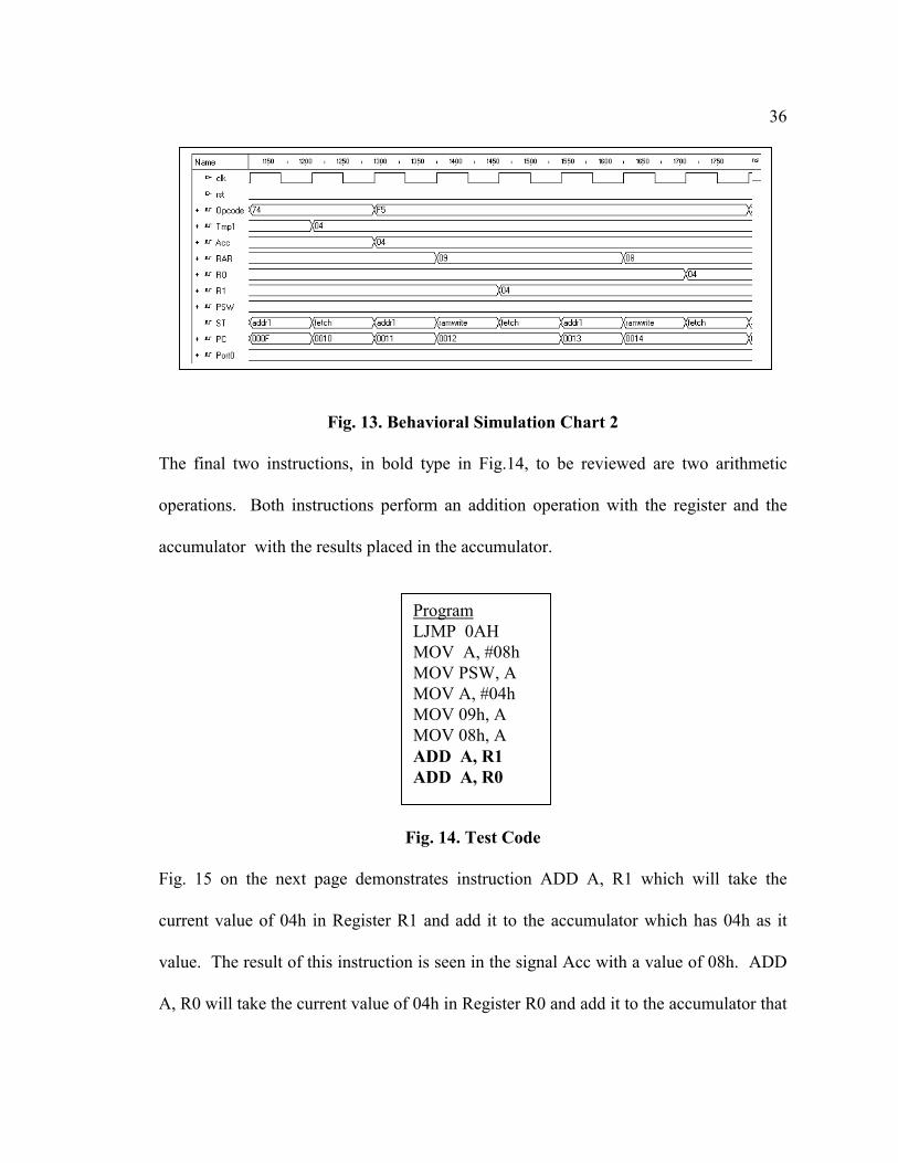
Fig. 13. Behavioral Simulation Chart 2
The final two instructions, in bold type in Fig.14, to be reviewed are two arithmetic
operations. Both instructions perform an addition operation with the register and the
accumulator with the results placed in the accumulator.
Fig. 14. Test Code
Fig. 15 on the next page demonstrates instruction ADD A, R1 which will take the
current value of 04h in Register R1 and add it to the accumulator which has 04h as it
value. The result of this instruction is seen in the signal Acc with a value of 08h. ADD
A, R0 will take the current value of 04h in Register R0 and add it to the accumulator that
ProgramLJMP 0AHMOV A, #08hMOV PSW, AMOV A, #04hMOV 09h, AMOV 08h, AADD A, R1ADD A, R0

37
has 08h as it contents. The result of this instruction is seen in signal Acc. Acc changes
to 0Ch.
Fig. 15. Behavioral Simulation Chart 3
In summary, it has been demonstrated that the VHDL Behavioral model that
produced the above simulation charts correctly executes the instructions that were
chosen to be modeled.

38
7.0 IS Model and Simulation Results
The simulation results of chapter 6 have shown that the mini-instruction set
Behavioral model of the Intel 8031 behaved correctly, as far as functionality is
concerned. When reviewing the simulations with respect to timing, the waveforms are
no where close to meeting the timing diagrams as specified by the Intel 8031 databook
[5]. In translating the Behavioral model to an IS model much attention was paid to the
timing characteristics of the microcontroller. The IS model needs to match the relative
timing as seen in chapter 3.
Table 7. T Cycles and RTN for ADD,Rn
ALE .PSEN P0Lat RTN
T1 0 0 1T2 1 1 0 PC ← PA; PCinc ← PCT3 1 1 0 P0,P2 ← PA; PC + 1T4 0 1 0 PC ← PCincT5 0 0 0 P0 ← High ZT6 0 0 0T7 0 0 1T8 1 1 0 IR←P0LatT9 1 1 0 RamAddReg ← (Rn); TMP2 ← ACCT10 0 1 0 TMP1 ← Ram(Rn)T11 0 0 0 ALUout ← TMP1 + TMP2T12 0 0 0 ACC ← ALUout
Table 7 shows a T cycle table along with the critical control signals and their
associated register transfers. Table 7 shown is for any ADD, Rn instruction. A table
similar to this one was constructed for other single machine cycle instructions and for
dual machine cycle instructions. As directed by the Intel data book, a single machine
39
cycle is broken into twelve evenly time-spaced steps. A blank table was constructed
with twelve lines. Details were added to the table as extracted from the Intel
8031datasheet timing diagrams. In particular, the Address Latch Enable (ALE) and
Program Store Enable active low (PSENn) signals that are critical to external memory
fetches were included. If the timing of the ALE and PSENn signals are not correct then
the IS model is worthless, i.e. the microcontroller will not properly interface with the
external memory leaving the microcontroller “brain dead”. In table 7 the ALE and
PSENn columns have a 1 or 0 depending on Intel specified relative timing. See lines
454-489 of appendix D to see an example of how ALE and PSENn are toggled. The
P0Latch column shows an entry of 1 were the data should be sampled from the external
memory bus.
After building all of the RTN tables for several instructions, the IS model was
constructed. Instead of having a cycle or state for the action needed to complete each
instruction as with the Behavioral model, the IS model has a state machine with 24
states. If an instruction is termed a single machine cycle instruction then that instruction,
through decoding, directs the state machine to use 12 cycles. If an instruction is termed
a two-machine cycle instruction then that instruction will cause the state machine to
cycle through 24 states. This will become apparent to the reader during the discussion of
the simulation results. In the IS VHDL model each state of the CPU state machine
process was named with much detail. This allowed for easier debugging (see lines 96-
110 appendix D). As a consequence, the state names will not be visible in the
simulations shown in the next section.
40
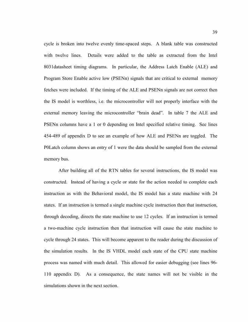
7.1 IS Model Simulation Results with Behavioral Code
Before explaining the results of the IS model, the timing of the instruction
interactions should be discussed. In Fig. 16 below, one will notice that with the IS
VHDL model the ST signal is comprised of many states. See lines 96-110 of appendix
D to view the state names used. There is also activity on Port 0 and Port 2 that was not
present in the Behavioral model. This port activity indicates that the IS model is
interacting with the test bench and retrieving instructions from the virtual ROM. Also
included on the simulation figures for the IS model are the signals ALE and PSENn.
The activity on these signals also indicate that the IS model is communicating with the
virtual external ROM.
Fig. 16. IS Model Simulation Chart 1
The simulation results shown in Fig. 16 are similar to those for the Behavioral
model and also cover the same first three instructions, a LJMP and two MOV’s. Again
we see that the end result of processing the LJMP instruction is that the PC is
incremented to 0Ah. The first instruction, MOV A, #08h, completes as before with the
value of 08h being transferred while the next instruction is being fetched. The third

41
instruction, MOV PSW, A, completes with the PSW register updated to a value of 08h
as instructed.
The results for the next three instructions, entries in bold type in Fig. 17, are
displayed in Fig. 18. The MOV A, #04h instruction executes with the same results as in
the Behavioral model; the accumulator is updated with 08h. The next two MOV
instructions are identical to those used before except for the specified destination
registers. Both registers R1 and R0 of register bank 0 receive the value of 04h.
Fig. 17. Test Code
Fig. 18. IS Model Simulation Chart 2
ProgramLJMP 0AHMOV A, #08hMOV PSW, AMOV A, #04hMOV 09h, AMOV 08h, AADD A, R1ADD A, R0

42
The last two instructions of the test of code, as indicated by the bold type in Fig. 19,
are arithmetic instructions. In Fig. 20, registers R1 and R0 of register bank zero are
updated with the results from the ALU. The value stored in R1, 04h, is added to the
accumulator and the result of the addition stored in the accumulator. The ADD A, R0
instruction operates the same way except targeting register R0. As a result the final
value of the accumulator should be 0Ch and is. This result compares with Behavioral
model result.
Fig. 19. Test Code
Fig. 20. IS Model Simulation Chart 3
ProgramLJMP 0AHMOV A, #08hMOV PSW, AMOV A, #04hMOV 08h, AMOV 09h, AADD A, R1ADD A, R0
43
7.2 IS Model Simulation Results with R0 Test Code
In the previous section, simulation results were shown for a simple eight-
instruction program. A more exhaustive test of the register addressing instructions was
completed. A program with 54 instructions was loaded by the test bench and re-
simulated. A complete listing of the program used for IS model testing can be found in
appendix B. For this test sequence, the results obtained from the hardware modeler,
referred to as the “golden code” for the same 54 instructions, were used for comparison.
A couple of the instructions for this new test sequence will be discussed in this section.
A complete set of results for the IS model tests can be found in appendix C.
Fig. 21 shows again the beginning of the test program. This new program, like
the last program, begins with a LJMP instruction. In Fig. 21 there are a couple new
signals not present in all previous simulation charts.
Fig. 21. IS Model Simulation Chart 4
44
The signals with the suffix _HW are signals that were played back from a text file as the
simulation was running. The text file was generated from running the hardware modeler
with the same program except the results were recorded from an actual Intel 8031
microcontroller. The signal results recorded from the real Intel 8031 are termed “golden
vectors”. This process of playing the “golden vectors” against the IS model was decided
to be the verification method. While the hardware modeler does not allow access to the
internal registers of the actual Intel 8031, results of all port activities were recorded.
Since the internal register activity can not be viewed, instructions were chosen to
exercise the ALU and the like and the results were observed on Port1. So if an addition
instruction was executed the next instruction would be a port write instruction to see if
the IS model would output the same result as the Intel 8031 chip as represented by the
signals with the _HW extension.
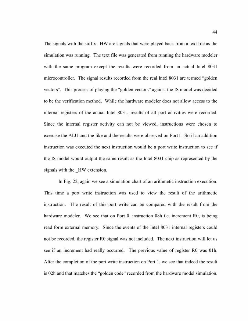
In Fig. 22, again we see a simulation chart of an arithmetic instruction execution.
This time a port write instruction was used to view the result of the arithmetic
instruction. The result of this port write can be compared with the result from the
hardware modeler. We see that on Port 0, instruction 08h i.e. increment R0, is being
read form external memory. Since the events of the Intel 8031 internal registers could
not be recorded, the register R0 signal was not included. The next instruction will let us
see if an increment had really occurred. The previous value of register R0 was 01h.
After the completion of the port write instruction on Port 1, we see that indeed the result
is 02h and that matches the “golden code” recorded from the hardware model simulation.

45
Fig. 22. IS Model Simulation Chart 5
As previously mentioned, the program for this test sequence contains 54
instructions. The remaining simulation results are similar to what has been presented
here. See appendix C for a complete set of simulation charts. In summary, all tested
instructions matched the results from the hardware modeler. The results obtained here
greatly support the statement; the IS model developed in this research is an accurate
model of the Intel 8031 for the instructions modeled.

46
8.0 Summary and Future Work
This thesis has detailed the results of creating and simulating 2 VHDL models for
the Intel 8031. These models were written to help support an effort to eradicate the
component obsolescence problem faced by the U.S. government. A simple Behavioral
model was written and tested to verify proper abstract modeling. Next, an Instruction
Set (IS) model was written for one half of the instruction set of the Intel 8031. The IS
model results were compared against the results from an actual Intel 8031 accessed and
simulated by using a Hardware Modeler made by Synopsys. For the modeled
instructions, it was found that the IS model accurately emulates the functionality of the
original Intel 8031. The efforts of this research will help support the overall goal to
fabricate an 8-bit microcontroller that emulates with form, fit, and function the original
Intel 8031 microcontroller.
Continuation of this research will be carried out at Ohio University. Items to
research and complete include: finishing the IS model, writing an RTL model,
synthesizing the RTL model, and testing all models. Some of this work has been
completed, but was not documented in this thesis. RTL models and synthesis results
have been made available to Dr. Starzyk.

47
References
[1] C. H. Roth, Jr., Digital Systems Design Using VHDL, PWS Publishing
Company, Boston, Copyright1998 pp. 387-411.
[2] J. Bhasker, A VHDL Primer, Prentice-Hall, Inc. , New Jersey, Copyright 1995 pp
2-3.
[3] Synopsys, Logic Modeling Development Manual, Synopsys, Inc. Copyright
1994. pp. 1-2.
[4] IEEE Standard VHDL Language Reference Manual, Std 1076-1993, IEEE, New
York, 1993.
[5] Intel, Embedded Microcontrollers and Processors Vol. I, Intel Corporation, 1993
pp. 5.3-5.17, 6.1 – 6.75, 7.1 – 7.34.
[6] D. Barker, “Why Are People Always Talking About VHDL” Air Force Research
Laboratory Article, Wright-Patterson Air Force Base, Ohio, 1999. pp. 2-5.

48
Appendix A - Intel 8031 INSTRUCTION SET
Instruction Opcodes in Hexadecimal Order
Hex Code Number of Bytes Mnemonic Operands00 1 NOP01 2 AJMP code addr02 3 LJMP code addr03 1 RR A04 1 INC A05 2 INC data addr06 1 INC @R007 1 INC @R108 1 INC R009 1 INC R10A 1 INC R20B 1 INC R30C 1 INC R40D 1 INC R50E 1 INC R60F 1 INC R710 3 JBC bit addr, code addr11 2 ACALL code addr12 3 LCALL code addr13 1 RRC A14 1 DEC A15 2 DEC data addr16 1 DEC @R017 1 DEC @R118 1 DEC R019 1 DEC R11A 1 DEC R21B 1 DEC R31C 1 DEC R41D 1 DEC R51E 1 DEC R61F 1 DEC R7

49
Appendix A - Intel 8031 INSTRUCTION SET
Instruction Opcodes in Hexadecimal Order (Continued)
Hex Code Number of Bytes Mnemonic Operands20 3 JB bit addr, code addr21 2 AJMP code addr22 1 RET23 1 RL A24 2 ADD A, # data25 2 ADD A, data addr26 1 ADD A, @ R027 1 ADD A, @ R128 1 ADD A,R029 1 ADD A,R12A 1 ADD A,R22B 1 ADD A,R32C 1 ADD A,R42D 1 ADD A,R52E 1 ADD A,R62F 1 ADD A,R730 3 JNB bit addr, code addr31 2 ACALL code addr32 1 RETI33 1 RLC A34 2 ADDC A, # data35 2 ADDC A, data addr36 1 ADDC A, @ R037 1 ADDC A, @ R138 1 ADDC A,R039 1 ADDC A,R13A 1 ADDC A,R23B 1 ADDC A,R33C 1 ADDC A,R43D 1 ADDC A,R53E 1 ADDC A,R63F 1 ADDC A,R7

50
Appendix A - Intel 8031 INSTRUCTION SET
Instruction Opcodes in Hexadecimal Order (Continued)
Hex Code Number of Bytes Mnemonic Operands40 2 JC code addr41 2 AJMP code addr42 2 ORL data addr, A43 3 ORL data addr, # data44 2 ORL A, # data45 2 ORL A, data addr46 1 ORL A, @ R047 1 ORL A, @ R148 1 ORL A,R049 1 ORL A,R14A 1 ORL A,R24B 1 ORL A,R34C 1 ORL A,R44D 1 ORL A,R54E 1 ORL A,R64F 1 ORL A,R750 2 JNC code addr51 2 ACALL code addr52 2 ANL data addr, A53 3 ANL data addr, # data54 2 ANL A, # data55 2 ANL A, data addr56 1 ANL A, @ R057 1 ANL A, @ R158 1 ANL A,R059 1 ANL A,R15A 1 ANL A,R25B 1 ANL A,R35C 1 ANL A,R45D 1 ANL A,R55E 1 ANL A,R65F 1 ANL A,R7

51
Appendix A - Intel 8031 INSTRUCTION SET
Instruction Opcodes in Hexadecimal Order (Continued)
Hex Code Number of Bytes Mnemonic Operands60 2 JZ code addr61 2 AJMP code addr62 2 XRL data addr, A63 3 XRL data addr, # data64 2 XRL A, # data65 2 XRL A, data addr66 1 XRL A, @ R067 1 XRL A, @ R168 1 XRL A,R069 1 XRL A,R16A 1 XRL A,R26B 1 XRL A,R36C 1 XRL A,R66D 1 XRL A,R56E 1 XRL A,R66F 1 XRL A,R770 2 JNZ code addr71 2 ACALL code addr72 2 ORL C,bit addr73 1 JMP @A + DPTR74 2 MOV A, # data75 3 MOV data addr, # data76 2 MOV @ R0, # data77 2 MOV @ R1, # data78 2 MOV R0, # data79 2 MOV R1, # data7A 2 MOV R2, # data7B 2 MOV R3, # data7C 2 MOV R4, # data7D 2 MOV R5, # data7E 2 MOV R6, # data7F 2 MOV R7, # data

52
Appendix A - Intel 8031 INSTRUCTION SET
Instruction Opcodes in Hexadecimal Order (Continued)
Hex Code Number of Bytes Mnemonic Operands80 2 SJMP code addr81 2 AJMP code addr82 2 ANL C,bit addr83 1 MOVC A,@A + PC84 1 DIV AB85 3 MOV data addr, data addr86 2 MOV data addr, @ R087 2 MOV data addr, @ R188 2 MOV data addr,R089 2 MOV data addr,R18A 2 MOV data addr,R28B 2 MOV data addr,R38C 2 MOV data addr,R88D 2 MOV data addr,R58E 2 MOV data addr,R88F 2 MOV data addr,R790 3 MOV code addr91 2 ACALL code addr92 2 MOV C,bit addr93 1 MOVC @A + DPTR94 2 SUBB A, # data95 2 SUBB data addr, # data96 1 SUBB @ R0, # data97 1 SUBB @ R1, # data98 1 SUBB R0, # data99 1 SUBB R1, # data9A 1 SUBB R2, # data9B 1 SUBB R3, # data9C 1 SUBB R4, # data9D 1 SUBB R5, # data9E 1 SUBB R8, # data9F 1 SUBB R7, # data

53
Appendix A - Intel 8031 INSTRUCTION SET
Instruction Opcodes in Hexadecimal Order (Continued)
Hex Code Number of Bytes Mnemonic OperandsA0 2 ORL C,/bit addrA1 2 AJMP code addrA2 2 MOV C,bit addrA3 1 INC DPTRA4 1 MUL ABA5 reservedA6 2 MOV @ R0, data addrA7 2 MOV @ R1, data addrA8 2 MOV R0, data addrA9 2 MOV R1, data addrAA 2 MOV R2, data addrAB 2 MOV R3, data addrAC 2 MOV R4, data addrAD 2 MOV R5, data addrAE 2 MOV R6, data addrAF 2 MOV R7, data addrB0 2 ANL C,/bit addrB1 2 ACALL code addrB2 2 CPL bit addrB3 1 CPL CB4 3 CJNE A, # data, code addrB5 3 CJNE A, data addr, code addrB6 3 CJNE @ R0, # data, code addrB7 3 CJNE @ R1, # data, code addrB8 3 CJNE R0, # data, code addrB9 3 CJNE R1, # data, code addrBA 3 CJNE R2, # data, code addrBB 3 CJNE R3, # data, code addrBC 3 CJNE R4, # data, code addrBD 3 CJNE R5, # data, code addrBE 3 CJNE R8, # data, code addrBF 3 CJNE R7, # data, code addr

54
Appendix A - Intel 8031 INSTRUCTION SET
Instruction Opcodes in Hexadecimal Order (Continued)
Hex Code Number of Bytes Mnemonic OperandsC0 2 PUSH data addrC1 2 AJMP code addrC2 2 CLR bit addrC3 1 CLR CC4 1 SWAP AC5 2 XCH A, data addrC6 1 XCH A,@ R0C7 1 XCH A,@ R1C8 1 XCH A,R0C9 1 XCH A,R1CA 1 XCH A,R2CB 1 XCH A,R3CC 1 XCH A,R4CD 1 XCH A,R5CE 1 XCH A,R6CF 1 XCH A,R7D0 2 POP data addrD1 2 ACALL code addrD2 2 SETB bit addrD3 1 SETB CD4 1 DA AD5 3 DJNZ data addr, code addrD6 1 XCHD A,@ R0D7 1 XCHD A,@ R1D8 2 DJNZ R0, code addrD9 2 DJNZ R1, code addrDA 2 DJNZ R2, code addrDB 2 DJNZ R3, code addrDC 2 DJNZ R4, code addrDD 2 DJNZ R5, code addrDE 2 DJNZ R6, code addrDF 2 DJNZ R7, code addr

55
Appendix A - Intel 8031 INSTRUCTION SET
Instruction Opcodes in Hexadecimal Order (Continued)
Hex Code Number of Bytes Mnemonic OperandsE0 1 MOVX A, @ DPTRE1 2 AJMP code addrE2 1 MOVX A, @ R0E3 1 MOVX A, @ R1E4 1 CLR AE5 2 MOV A, data addrE6 1 MOV A,@ R0E7 1 MOV A,@ R1E8 1 MOV A,R0E9 1 MOV A,R1EA 1 MOV A,R2EB 1 MOV A,R3EC 1 MOV A,R4ED 1 MOV A,R5EE 1 MOV A,R6EF 1 MOV A,R7F0 1 MOVX code addrF1 2 ACALL code addrF2 1 MOVX C,bit addrF3 1 MOVX @A + DPTRF4 1 CPL A, # dataF5 2 MOV data addr, AF6 1 MOV @ R0, AF7 1 MOV @ R1, AF8 1 MOV R0,AF9 1 MOV R1,AFA 1 MOV R2,AFB 1 MOV R3,AFC 1 MOV R4,AFD 1 MOV R5,AFE 1 MOV R6,AFF 1 MOV R7,A

56
Appendix B - Instruction Set Model Test Code
This following test program was used to test the Register 0 Register Addressing Mode.Results from this test code are available in Appendix C.
Reg RTN Mnemonic Operands Op CodeStatus
A = 01h A ← #01h MOV A, #01h 74 01R0 = 1d R0 ← A MOV 08, A F5 08P1 = 1d P1 ← R0 MOV 90, R0 88 90
R0 = 2d INC R0 08P1 = 2d P1 ← R0 MOV 90, R0 88 90
R0 = 1d DEC R0 18P1 = 1d P1 ← R0 MOV 90, R0 88 90
A = 2d ADD A, R0 28P1 = 2d P1 ← A MOV 90, A F5 90
C = 1 C ← 1 SETB C D3A = 4d A ← A + C + R0 ADDC A, R0 38P1 = 4d P1 ← A MOV 90, A F5 90
A ← 5d ORL A, R0 48P1 = 5d P1 ← A MOV 90, A F5 90
A ← 1d ANL A, R0 58P1 = 1d P1 ← A MOV 90, A F5 90
A ← 00h XRL A, R0 68P1 = 00h P1 ← A MOV 90, A F5 90
R0 ← 20h MOV R0, #20h 78 20P1 = 20h P1 ← R0 MOV 90, R0 88 90

57
Appendix B - Instruction Set Model Test Code
Reg RTN Mnemonic Operands Op CodeStatus
A ← R0 MOV A, R0 E8P1 = 20h P1 ← A MOV 90, A F5 90
R0 ← 0Bh MOV R0, #0Bh 78 0BP1 = 0Bh P1 ← R0 MOV 90, R0 88 90
C ← 0 CLR C C3C ← 1 SETB C D3A ← A - C - R0 SUBB A, R0 98
P1 = 14h P1 ← A MOV 90, A F5 90
R0 ← #22h MOV R0, #22h 78 22B3 = 22h B3 ← R0 MOV B3, R0 88 B3
R0 ← #48h MOV R0, #48h 78 48R0 ← B3 MOV R0, B3 A8 B3
P1 = 22h P1 ← R0 MOV 90, R0 88 90
R0 = 01h R0 ← #01h MOV R0, #01h 78 01DJNZ R0, 10h D8 10
R0 = 02h R0 ← #02h MOV R0, #02h 78 02DJNZ R0, 10h D8 04
00 0000 00
R0 = #48h R0 ← #48h MOV R0, #48h 78 48CJNE R0, #48h B8 48 04 CJNE R0, #50h B8 50 04
00 0000 00
R0 = 03h R0 ← #03h MOV R0, #03h 78 03A = 0Ch A ← 0Ch MOV A, 0Ch 74 0C
XCH A, R0 C8P1 = 03h P1 ← A MOV 90, A F5 90P1 = 0Ch P1 ← R0 MOV 90, R0 88 90

58
Appendix B - Instruction Set Model Test Code
Reg RTN Mnemonic Operands Op CodeStatus
R0 = #05h R0 ← #05h MOV R0, #05h 78 05A = #09h A ← #09h MOV A, #09h 74 09
MOV A, R0 E8P1 = 05h P1 ← A MOV 90, A F5 90
R0 = #02h R0 ← #02h MOV R0, #02h 78 02A = #04h A ← #04h MOV A, #04h 74 04
MOV R0, A F8P1 = 04h P1 ← R0 MOV 90, R0 88 90

59
Appendix C - Instruction Set Model Simulation Results with Test Code
Reg RTN Mnemonic Operands Op CodeStatus
A = 01h A ← #01h MOV A, #01h 74 01R0 = 1d R0 ← A MOV 08, A F5 08P1 = 1d P1 ← R0 MOV 90, R0 88 90

60
Appendix C - Instruction Set Model Simulation Results with Test Code
Reg RTN Mnemonic Operands Op CodeStatus
R0 = 1d DEC R0 18P1 = 1d P1 ← R0 MOV 90, R0 88 90

61
Appendix C - Instruction Set Model Simulation Results with Test Code
Reg RTN Mnemonic Operands Op CodeStatus
R0 = 2d INC R0 08P1 = 2d P1 ← R0 MOV 90, R0 88 90
62
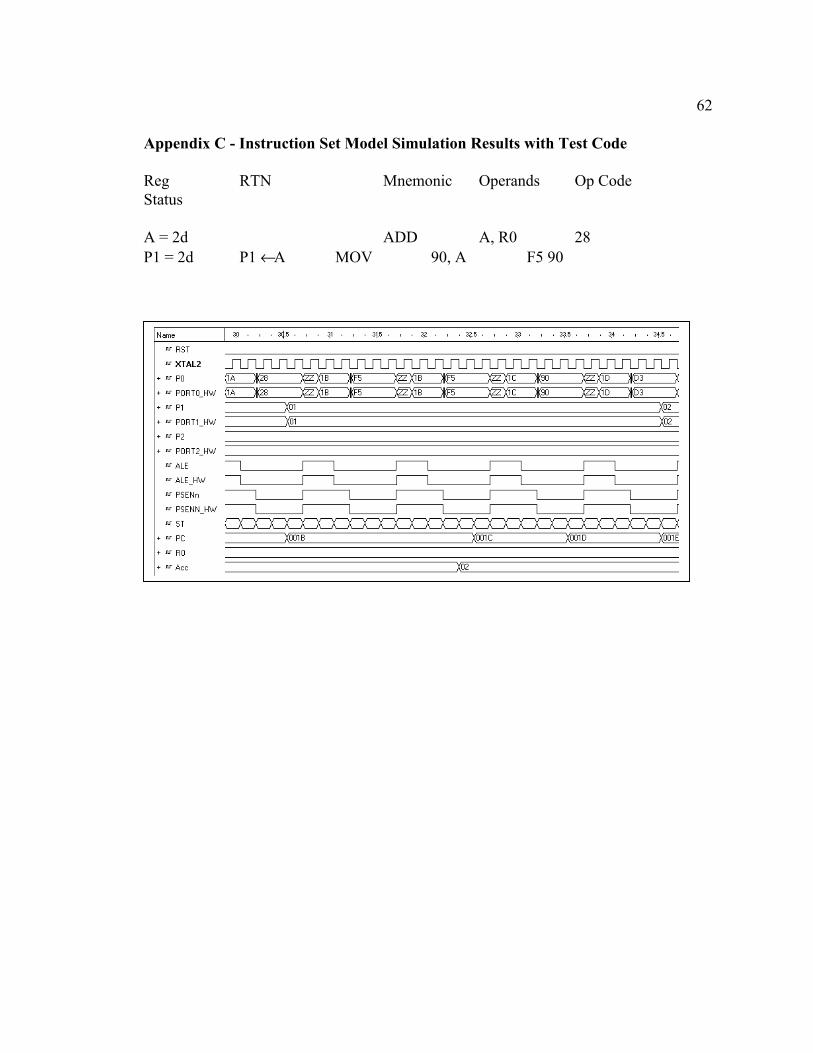
Appendix C - Instruction Set Model Simulation Results with Test Code
Reg RTN Mnemonic Operands Op CodeStatus
A = 2d ADD A, R0 28P1 = 2d P1 ← A MOV 90, A F5 90

63
Appendix C - Instruction Set Model Simulation Results with Test Code
Reg RTN Mnemonic Operands Op CodeStatus
C = 1 C ← 1 SETB C D3A = 4d A ← A + C + R0 ADDC A, R0 38P1 = 4d P1 ← A MOV 90, A F5 90

64
Appendix C - Instruction Set Model Simulation Results with Test Code
Reg RTN Mnemonic Operands Op CodeStatus
A ← 5d ORL A, R0 48P1 = 5d P1 ← A MOV 90, A F5 90

65
Appendix C - Instruction Set Model Simulation Results with Test Code
Reg RTN Mnemonic Operands Op CodeStatus
A ← 1d ANL A, R0 58P1 = 1d P1 ← A MOV 90, A F5 90

66
Appendix C - Instruction Set Model Simulation Results with Test Code
Reg RTN Mnemonic Operands Op CodeStatus
A ← 00h XRL A, R0 68P1 = 00h P1 ← A MOV 90, A F5 90

67
Appendix C - Instruction Set Model Simulation Results with Test Code
Reg RTN Mnemonic Operands Op CodeStatus
R0 ← 20h MOV R0, #20h 78 20P1 = 20h P1 ← R0 MOV 90, R0 88 90
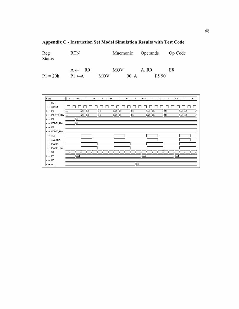
68
Appendix C - Instruction Set Model Simulation Results with Test Code
Reg RTN Mnemonic Operands Op CodeStatus
A ← R0 MOV A, R0 E8P1 = 20h P1 ← A MOV 90, A F5 90

69
Appendix C - Instruction Set Model Simulation Results with Test Code
Reg RTN Mnemonic Operands Op CodeStatus
R0 ← 0Bh MOV R0, #0Bh 78 0BP1 = 0Bh P1 ← R0 MOV 90, R0 88 90

70
Appendix C - Instruction Set Model Simulation Results with Test Code
Reg RTN Mnemonic Operands Op CodeStatus
C ← 0 CLR C C3C ← 1 SETB C D3A ← A - C - R0 SUBB A, R0 98
P1 = 14h P1 ← A MOV 90, A F5 90

71
Appendix C - Instruction Set Model Simulation Results with Test Code
Reg RTN Mnemonic Operands Op CodeStatus
R0 ← #22h MOV R0, #22h 78 22B3 = 22h B3 ← R0 MOV B3, R0 88 B3
R0 ← #48h MOV R0, #48h 78 48R0 ← B3 MOV R0, B3 A8 B3
P1 = 22h P1 ← R0 MOV 90, R0 88 90

72
Appendix C - Instruction Set Model Simulation Results with Test Code
Reg RTN Mnemonic Operands Op CodeStatus
R0 = 01h R0 ← #01h MOV R0, #01h 78 01DJNZ R0, 10h D8 10
R0 = 02h R0 ← #02h MOV R0, #02h 78 02DJNZ R0, 10h D8 04

73
Appendix C - Instruction Set Model Simulation Results with Test Code
Reg RTN Mnemonic Operands Op CodeStatus
DJNZ R0, 10h D8 0400 0000 00
R0 = #48h R0 ← #48h MOV R0, #48h 78 48

74
Appendix C - Instruction Set Model Simulation Results with Test Code
Reg RTN Mnemonic Operands Op CodeStatus
R0 = #48h R0 ← #48h MOV R0, #48h 78 48CJNE R0, #48h B8 48 04CJNE R0, #50h B8 50 04

75
Appendix C - Instruction Set Model Simulation Results with Test Code
Reg RTN Mnemonic Operands Op CodeStatus
CJNE R0, #50h B8 50 0400 0000 00
R0 = 03h R0 ← #03h MOV R0, #03h 78 03
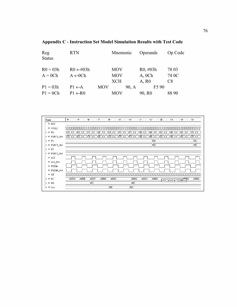
76
Appendix C - Instruction Set Model Simulation Results with Test Code
Reg RTN Mnemonic Operands Op CodeStatus
R0 = 03h R0 ← #03h MOV R0, #03h 78 03A = 0Ch A ← 0Ch MOV A, 0Ch 74 0C
XCH A, R0 C8P1 = 03h P1 ← A MOV 90, A F5 90P1 = 0Ch P1 ← R0 MOV 90, R0 88 90
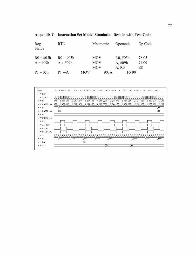
77
Appendix C - Instruction Set Model Simulation Results with Test Code
Reg RTN Mnemonic Operands Op CodeStatus
R0 = #05h R0 ← #05h MOV R0, #05h 78 05A = #09h A ← #09h MOV A, #09h 74 09
MOV A, R0 E8P1 = 05h P1 ← A MOV 90, A F5 90

78
Appendix C - Instruction Set Model Simulation Results with Test Code
Reg RTN Mnemonic Operands Op CodeStatus
R0 = #02h R0 ← #02h MOV R0, #02h 78 02A = #04h A ← #04h MOV A, #04h 74 04
MOV R0, A F8P1 = 04h P1 ← R0 MOV 90, R0 88 90
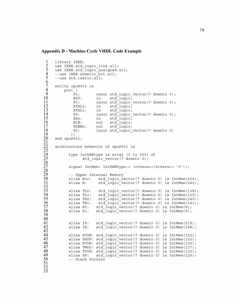
79
Appendix D - Machine Cycle VHDL Code Example
library IEEE;1use IEEE.std_logic_1164.all;2use IEEE.std_logic_unsigned.all;3--use IEEE.numeric_bit.all;4--use std.textio.all;5
6entity cpu8031 is7
port (8P1: inout std_logic_vector(7 downto 0);9RST: in std_logic;10P3: inout std_logic_vector(7 downto 0);11XTAL2: in std_logic;12XTAL1: in std_logic;13P0: inout std_logic_vector(7 downto 0);14EAn: in std_logic;15ALE: out std_logic;16PSENn: out std_logic;17P2: inout std_logic_vector(7 downto 0)18
);19end cpu8031;20
21architecture behavior of cpu8031 is22
23type IntRAMtype is array (0 to 255) of24
std_logic_vector(7 downto 0);2526
signal IntMem: IntRAMtype:= (others=>(others=> '0'));2728
-- Upper Internal Memory29alias Acc: std_logic_vector(7 downto 0) is IntMem(224);30alias B: std_logic_vector(7 downto 0) is IntMem(240);31
32alias TL0: std_logic_vector(7 downto 0) is IntMem(138);33alias TL1: std_logic_vector(7 downto 0) is IntMem(139);34alias TH0: std_logic_vector(7 downto 0) is IntMem(140);35alias TH1: std_logic_vector(7 downto 0) is IntMem(141);36alias R0: std_logic_vector(7 downto 0) is IntMem(8);37alias R1: std_logic_vector(7 downto 0) is IntMem(9);38
3940
alias IP: std_logic_vector(7 downto 0) is IntMem(219);41alias IE: std_logic_vector(7 downto 0) is IntMem(168);42
43alias SCON: std_logic_vector(7 downto 0) is IntMem(152);44alias SBUF: std_logic_vector(7 downto 0) is IntMem(153);45alias PCON: std_logic_vector(7 downto 0) is IntMem(135);46alias TMOD: std_logic_vector(7 downto 0) is IntMem(137);47alias TCON: std_logic_vector(7 downto 0) is IntMem(136);48alias SP: std_logic_vector(7 downto 0) is IntMem(129);49-- Stack Pointer50
515253

80
alias DPH: std_logic_vector(7 downto 0) is IntMem(131);54-- Data Pointer High byte55
56alias DPL: std_logic_vector(7 downto 0) is IntMem(130);57-- Data Pointer Low byte58
59alias PSW: std_logic_vector(7 downto 0) is IntMem(208);60-- Program Status Word61
62alias CY: std_logic is PSW(7); -- Carry Flag63alias AC: std_logic is PSW(6); -- Auxiliary Carry Flag64alias FO: std_logic is PSW(5); -- Flag 065alias RS1: std_logic is PSW(4);66-- Register Bank selector bit 167
68alias RS0: std_logic is PSW(3);69-- Register Bank selector bit 070
71alias OV: std_logic is PSW(2); -- Overflow Flag72alias UD: std_logic is PSW(1); -- User definable flag73alias P: std_logic is PSW(0);74-- Parity Flag, Parity of Accumulator75
76alias Port0_Ram_Reg: std_logic_vector(7 downto 0) is77IntMem(128);78
79alias Port1_Ram_Reg: std_logic_vector(7 downto 0) is80IntMem(144);81
82alias Port2_Ram_Reg: std_logic_vector(7 downto 0) is83IntMem(160);84
85alias Port3_Ram_Reg: std_logic_vector(7 downto 0) is86IntMem(176);87
8889
alias R0RS00: std_logic_vector(7 downto 0) is IntMem(08);90alias R1RS00: std_logic_vector(7 downto 0) is IntMem(09);91
92939495
type state_type is (reset, fetch, addr1, addr2, data,96cycle8,cycle9,cycle10,97
98M1T1_fetch1,99M1T2_AleDrvHigh1,100M1T3_PcOut1,101M1T4_AleDrvLow1,102M1T5_PsenDrvLow1,103M1T6_Null1,104M1T7_fetch2,105M1T8_AleDrvHigh2,106M1T9_PcOut2,107M1T10_AleDrvLow2,108M1T11_PsenDrvLow2,109M1T12_Null2);110

81
signal ST, nST: state_type;111112113
signal IR : std_logic_vector(7 downto 0) := (others=> '0');114alias OP: std_logic_vector(3 downto 0) is IR(7 downto 4);115alias mode: std_logic_vector(3 downto 0) is IR(3 downto 0);116
117signal RAR: std_logic_vector(7 downto 0) := (others =>118'Z'); -- Ram Address Register119
120signal RARTemp: std_logic_vector(7 downto 0) := (others =>121'Z'); -- Ram Address Register122
123signal PC, PAR: std_logic_vector(15 downto 0);124
125alias PCH : std_logic_vector(7 downto 0) is126PC(15 downto 8);127-- Program Counter High128
129alias PCL : std_logic_vector(7 downto 0) is PC(7 downto 0);130-- Program Counter Low131
132alias PARH : std_logic_vector(7 downto 0) is133PAR(15 downto 8);134-- Program Address Register High135
136alias PARL : std_logic_vector(7 downto 0) is137PAR(7 downto 0);138-- Program Address Register Low139
140signal PCLtemp : std_logic_vector(7 downto 0);141signal PCHtemp : std_logic_vector(7 downto 0);142
143signal AluOutput : std_logic_vector(7 downto 0)144:= "00000000";145
146constant zero: std_logic_vector(7 downto 0) := "00000000";147
148subtype ot is std_logic_vector(3 downto 0);149
150-- upper 4 bits of opcode151
152constant ADD: ot:= "0010";153constant ADDC: ot:= "0011";154constant INC: ot:= "0000";155constant DEC: ot:= "0001";156constant ANL: ot:= "0101";157constant ORL: ot:= "0100";158constant XRL: ot:= "0110";159constant XCH: ot:= "1100";160constant MOVR2A: ot:= "1110";161constant MOVA2R: ot:= "1111";162constant MOVIMM2R: ot:= "0111";163constant MOVR2DIR: ot:= "1000";164constant MOVDIR2R: ot:= "1010";165
166

82
-- Register Addressing Operands167168
constant INC_REG: ot:= "0000";169constant DEC_REG: ot:= "0001";170constant ADD_REG: ot:= "0010";171constant ADDC_REG: ot:= "0011";172constant ORL_REG: ot:= "0100";173constant ANL_REG: ot:= "0101";174constant XRL_REG: ot:= "0110";175constant SUBB_REG: ot:= "1001";176constant XCH_REG: ot:= "1100";177constant DJNZ_REG: ot:= "1101";178constant CJNE_REG: ot:= "1011";179constant MOV_REG_A2R: ot:= "1110";180constant MOV_REG_R2A: ot:= "1111";181constant MOV_REG_IMM: ot:= "0111";182constant MOV_DIR_REG: ot:= "1000";183constant MOV_REG_DIR: ot:= "1010";184
185-- Immediate Addressing Operands186
187constant INC_IMM: ot := "0000"; -- Hex Code 04188constant DEC_IMM: ot := "0001"; -- Hex Code 12189constant ADD_IMM: ot := "0010"; -- Hex Code 24190constant MOV_IMM: ot := "0111"; -- Hex Code 74191
192-- Direct Addressing Operands;193
194constant ADD_DIR: ot := "0010";195constant MOV_DIR: ot := "1110";196constant MOV_DIR_ACC: ot:= "1111";197constant LJMP: ot := "0000";198constant SETB: ot := "1101";199-- Upper nibble for SETB opcode D3 HEX200constant CLRB: ot := "1100";201
-- Upper nibble for CLR C opcode C3 HEX202203
-- lower 4 bits of opcode204205
constant IMM: ot := "0100"; -- Immediate Addressing206207
constant DIR: ot := "0101"; -- Direct Addressing208209
constant MM2: ot := "0010"; -- Mix and Match Set 2210constant MM3: ot := "0011"; -- Mix and Match Set 3211
212constant IND0: ot := "0110"; -- Indirect Addressing R0213constant IND1: ot := "0111"; -- Indirect Addressing R1214
215constant REG0: ot := "1000"; -- Register Addressing R0216constant REG1: ot := "1001"; -- Register Addressing R1217constant REG2: ot := "1010"; -- Register Addressing R2218constant REG3: ot := "1011"; -- Register Addressing R3219constant REG4: ot := "1100"; -- Register Addressing R4220constant REG5: ot := "1101"; -- Register Addressing R5221constant REG6: ot := "1110"; -- Register Addressing R6222constant REG7: ot := "1111"; -- Register Addressing R7223
224

83
signal Opcode,Tmp1,Tmp2: std_logic_vector(7 downto 0);225226227
type decode_type is array (0 to 15) of228bit_vector(15 downto 0);229
230signal opd : bit_vector(15 downto 0);231
232constant decode: decode_type :=233(X"0001", X"0002", X"0004", X"0008",X"0010", X"0020",234X"0040", X"0080",235X"0100", X"0200", X"0400", X"0800",X"1000", X"2000",236X"4000", X"8000");237
238-- Data Registers and Control Signals239
240-- Data Registers241
242signal shiftout, op1, op2: std_logic_vector(7 downto 0):=243"00000000";244
245signal alu9: std_logic_vector(8 downto 0);246
247signal Cin : std_logic;248
249signal Read2ndByte: bit := '0';250signal Read3rdByte: bit := '0';251signal Read4thByte: bit := '0';252
253signal SecondByteDest: integer range 0 to 5 := 0;254
-- 0 = Discard255-- 1 = Tmp1256-- 2 = PCHtemp257-- 3 = RAR258-- 4 = PCLtemp -- for DJNZ code259-- 5 = Tmp2260
261signal ThirdByteDest: integer range 0 to 2 := 0;262
-- 0 = Discard263-- 1 = Tmp1264-- 2 = PCLtemp265
266signal FourthByteDest: integer range 0 to 3 := 0;267
-- 0 = Discard268-- 1 = Tmp1269-- 2 = PCLtemp270-- 3 = RAR271
signal MCycleLength: integer range 1 to 4 := 1;272-- 1 = 1 Machine Cycle273-- 2 = 2 Machine Cycles274-- 4 = 4 Machine Cycles275
276signal CycNum : integer := 0;277
278signal ChangeRAR : std_logic := '0';279-- this Rar Change sig is checked in M1T3280
281282

84
signal ChangeRAr2 :std_logic := '0';283-- this Rar Change sig is checked in M2T3284
285signal incPCxNO : std_logic := '0';286signal incPCx2 :std_logic := '0';287signal incPCx3 :std_logic := '0';288signal incPCx4 :std_logic := '0';289signal PCtemps2PC :std_logic := '0';290
291signal M1T1incPCxNO : std_logic := '0';292signal M1T1incPCx2 :std_logic := '0';293signal M1T1incPCx3 :std_logic := '0';294signal M1T1incPCx4 :std_logic := '0';295signal M1T1PCtemps2PC :std_logic := '0';296
297signal M1T7incPCxNO : std_logic := '0';298signal M1T7incPCx2 :std_logic := '0';299signal M1T7incPCx3 :std_logic := '0';300signal M1T7incPCx4 :std_logic := '0';301signal M1T7PCtemps2PC :std_logic := '0';302
303signal M2T1incPCxNO : std_logic := '0';304signal M2T1incPCx2 :std_logic := '0';305signal M2T1incPCx3 :std_logic := '0';306signal M2T1incPCx4 :std_logic := '0';307signal M2T1PCtemps2PC :std_logic := '0';308
309signal M2T7incPCxNO : std_logic := '0';310signal M2T7incPCx2 :std_logic := '0';311signal M2T7incPCx3 :std_logic := '0';312signal M2T7incPCx4 :std_logic := '0';313signal M2T7PCtemps2PC :std_logic := '0';314
315signal M2T7addPCxRel :std_logic := '0';316
317signal AccRamWrite : std_logic := '0';318signal RamReadTmp1 : std_logic := '0';319signal RamWrite : std_logic := '0';320signal RamWrite2 : std_logic := '0';321-- This Ram Write signal will be for 2 Cycle322-- instructions that need to write to the RAM323
324signal Updating_Port1_Driver : std_logic := '0';325signal Port1_Driver_NeedsUpdate : std_logic := '0';326signal SetCarry : std_logic := '0';327signal ClearCarry : std_logic := '0';328
329signal CurrentAluOutputNotZero : std_logic := '0';330signal UseRelOffset: std_logic := '0';331
332constant hi_Z8 : std_logic_vector(7 downto 0) :=333(others => 'Z');334constant hi_Z16 : std_logic_vector(15 downto 0) :=335(others => 'Z');336
337338339340

85
------------------------------------------------------341-- Begin Finite State Machine, i.e. CPU_Cycle Process342------------------------------------------------------343
344CPU_Cycles: process345
346variable reg_mem : Boolean;347
348variable CurrentInstLength: integer := 0;349
350begin351
352wait until XTAL2 = '0' and XTAL2'event;353
354355
if ((mode = IMM) or (mode = DIR) or (mode = REG0) or (mode =356REG1) or (mode = IND0)357
or (mode = IND1)) then358359
reg_mem:= true;360361
else362363
reg_mem:= false;364365
end if;366367368
if(RST = '1' ) then ST <= reset;369370
else371372
case ST is373374
-----------375-- RESET --376-----------377
378when reset =>379
380ST <= cycle8;381
382------------------------------383--384---- Machine Cycle 1385--386------------------------------387
388when M1T1_fetch1 => -- Machine Cycle 1, T Cycle 1389
390if RamWrite = '1' then391
report "Writing to Ram";392IntMem(CONV_INTEGER(RAR)) <= AluOutput;393
end if;394395396
if Port1_Driver_NeedsUpdate = '1' then397398

86
P1 <= Port1_Ram_Reg;399end if;400
401-----------------402-- Special increments for the PC403-----------------404
405if M1T1incPCx2 = '1' then406
407PC <= PC + 2; -- Increment PC by 2408report "Incrementing the PC by 2";409
410elsif M1T1incPCx3 = '1' then411
412PC <= PC + 3; -- Increment PC by 3413report "Incrementing the PC by 3";414
415elsif M1T1incPCx4 = '1' then416
417PC <= PC + 4; -- Increment PC by 4418report "Incrementing the PC by 4";419
420elsif M1T1PCtemps2PC = '1' then421
422423
PCH <= PCHtemp;424PCL <= PCLtemp;425report "Setting PC to Coded Value";426
427else428
429PC <= PC + 1; -- Increment PC by 1430report "incremening PC by 1";431
end if;432433
----------------434--End Special PC Incrementing435----------------436
437IR <= P0; -- Send Instruction to Instruction438
Register439440
ST <= M1T2_AleDrvHigh1;441442
when M1T2_AleDrvHigh1 => -- Machine Cycle 1, T Cycle 2443444
report "Current Stat is M1T2 / ";445446
if Updating_Port1_Driver <= '1' then447Updating_Port1_Driver <= '0';448
end if;449450
PAR <= PC;451-- Move PC Value to Program Address Register452
453ALE <= '1';454-- Set Address Latch Enable High455
456

87
PSENn <= '1';457-- Set Program Store Enable High458
459ST <= M1T3_PcOut1;460
461462
when M1T3_PcOut1 => -- Machine Cycle 1, T Cycle 3463464
if ChangeRAR = '1' then465RAR <= RARTemp;466
end if;467468
P0 <= PARL;469-- Move the Lower byte of PAR to Port 0470
471P2 <= PARH;472-- Move the Higher byte of PAR to Port 2473
474ST <= M1T4_AleDrvLow1;475
476when M1T4_AleDrvLow1 =>477
-- Machine Cycle 1, T Cycle 4478479
ALE <= '0';480-- Set Address Latch Enable Low481
482ST <= M1T5_PsenDrvLow1;483
484485
when M1T5_PsenDrvLow1 => -- Machine Cycle 1, T Cycle 5486487
P0 <= hi_Z8; -- Drive Port 0 to Z state488PSENn <= '0';489
490ST <= M1T6_Null1;491
492when M1T6_Null1 => -- Machine Cycle 1, T Cycle 6493
494if SetCarry = '1' then495
CY <= '1';496end if;497
498if ClearCarry = '1' then499
CY <= '0';500end if;501
502ST <= M1T7_fetch2;503
504when M1T7_fetch2 => -- Machine Cycle 1, T Cycle 7505
506If SecondByteDest = 0 then507
508report"Discard Current Byte";509
510elsif SecondByteDest = 1 then511
512Tmp1 <= P0;513
514

88
report " Second Byte Destination is Tmp1";515516517
elsif SecondByteDest = 2 then518519
PCHtemp <= P0;520521
report "Second Byte Destination is PCH temp";522523524
elsif SecondByteDest = 3 then525526
RAR <= P0;527528
report "Second Byte Destination is RAR";529530531
elsif SecondByteDest = 4 then532533
report "Second Byte Destination is PCL temp";534535
PCLtemp <= P0;536537
elsif SecondByteDest = 5 then538539
report "Secondbyte Destination is Tmp2 ";540541
Tmp2 <= P0;542543
end if;544545
-----------------546-- Special increments for the PC547-----------------548
549if M1T7incPCxNO = '1' then550
report "Not incrementing PC";551552
elsif M1T7incPCx2 = '1' then553554
PC <= PC + 2; -- Increment PC by 2555report "Incrementing the PC by 2";556
557elsif M1T7incPCx3 = '1' then558
559PC <= PC + 3; -- Increment PC by 3560report "Incrementing the PC by 3";561
562elsif M1T7incPCx4 = '1' then563
564PC <= PC + 4; -- Increment PC by 4565report "Incrementing the PC by 4";566
567elsif M1T7PCtemps2PC = '1' then568
569570
PCH <= PCHtemp;571PCL <= PCLtemp;572

89
report "Setting PC to Coded Value";573574
else575576
PC <= PC + 1; -- Increment PC by 1577report "Incrementing PC by 1";578
579end if;580
581------------------582----End Special PC Incrementing583------------------584
585ST <= M1T8_AleDrvHigh2;586
587when M1T8_AleDrvHigh2 => -- Machine Cycle 1, T Cycle 8588
589590
PAR <= PC;591-- Move Program Counter to Program Address Register592
593ALE <= '1';594-- Set Address Latch Enable High595
596PSENn <= '1';597
598ST <= M1T9_PcOut2;599
600when M1T9_PcOut2 => -- Machine Cycle 1, T Cycle 9601
602P0 <= PARL;603-- Move the Lower byte of PAR to Port 0604
605P2 <= PARH;606
607ST <= M1T10_AleDrvLow2;608
609when M1T10_AleDrvLow2 => -- Machine Cycle 1, T Cycle 10610
611ALE <= '0';612ST <= M1T11_PsenDrvLow2;613
614when M1T11_PsenDrvLow2 => -- Machine Cycle 1, T Cycle 11615
616P0 <= hi_Z8; -- Drive Port 0 to Z state617ST <= M1T12_Null2;618PSENn <= '0';619
620if RamReadTmp1 = '1' then621
report "Attempting RamReadTmp1";622Tmp1 <= IntMem(CONV_INTEGER(RAR));623
end if;624625
if AccRamWrite = '1' then626report "Attemping AccRamWrite";627IntMem(CONV_INTEGER(RAR)) <= Acc;628
end if;629630

90
when M1T12_Null2 => -- Machine Cycle 1, T Cycle 12631632
if reg_mem then633634
report "Attemping ALU_OP Call";635636
ALU_OP(Tmp1,Tmp2,Acc,AluOutput,CY,UseRelOffset);637638
end if;639640
IR <= "00000000"; -- Reset IR641642
if MCycleLength = 2 then643-- if the current opcode is a 2 cycle644-- instruction then go into M2645
646ST <= M2T1_fetch1;647report" transitioning to M2T1_fetch";648
else649650
ST <= M1T1_fetch1;651report "transitioning to M1T1_fetch";652
end if;653654
--------------------------------------------655-- End Machine Cycle 1656--------------------------------------------657
658
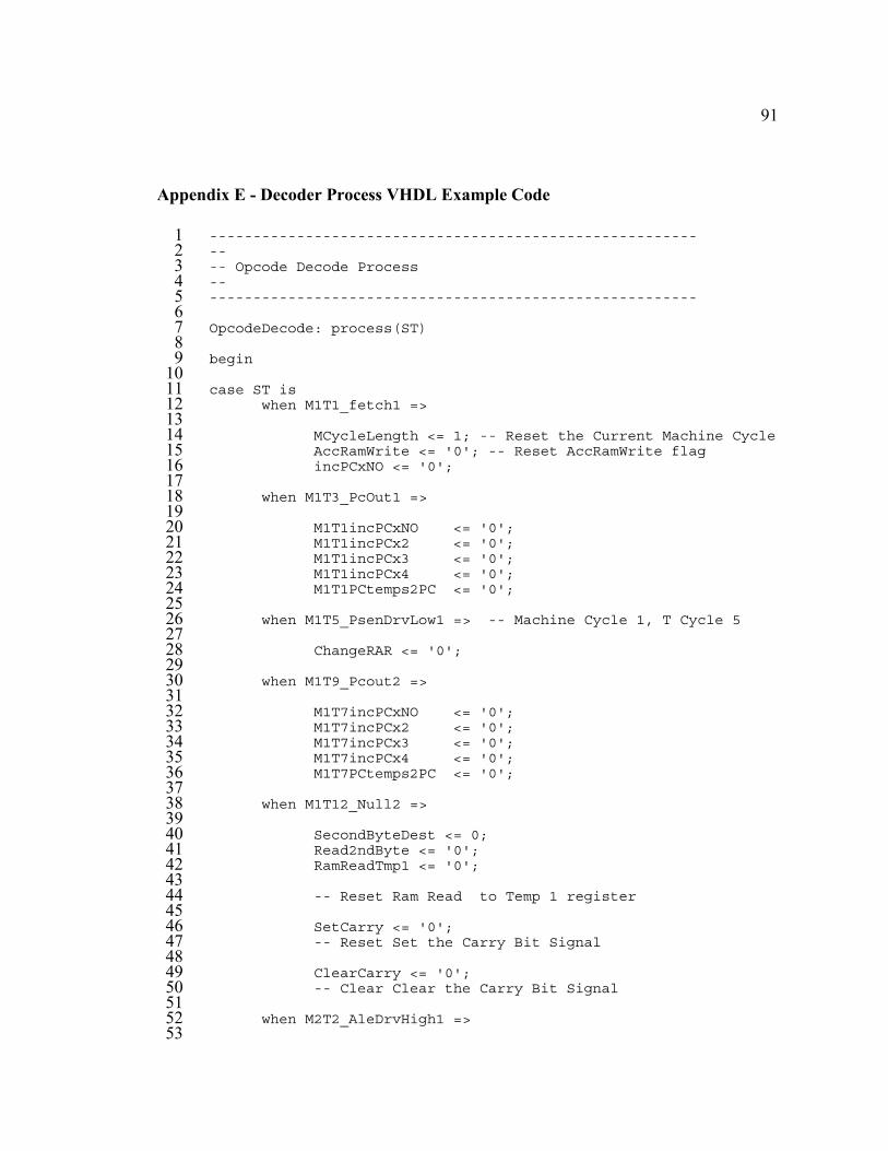
91
Appendix E - Decoder Process VHDL Example Code
--------------------------------------------------------1--2-- Opcode Decode Process3--4--------------------------------------------------------5
6OpcodeDecode: process(ST)7
8begin9
10case ST is11
when M1T1_fetch1 =>1213
MCycleLength <= 1; -- Reset the Current Machine Cycle14AccRamWrite <= '0'; -- Reset AccRamWrite flag15incPCxNO <= '0';16
17when M1T3_PcOut1 =>18
19M1T1incPCxNO <= '0';20M1T1incPCx2 <= '0';21M1T1incPCx3 <= '0';22M1T1incPCx4 <= '0';23M1T1PCtemps2PC <= '0';24
25when M1T5_PsenDrvLow1 => -- Machine Cycle 1, T Cycle 526
27ChangeRAR <= '0';28
29when M1T9_Pcout2 =>30
31M1T7incPCxNO <= '0';32M1T7incPCx2 <= '0';33M1T7incPCx3 <= '0';34M1T7incPCx4 <= '0';35M1T7PCtemps2PC <= '0';36
37when M1T12_Null2 =>38
39SecondByteDest <= 0;40Read2ndByte <= '0';41RamReadTmp1 <= '0';42
43-- Reset Ram Read to Temp 1 register44
45SetCarry <= '0';46-- Reset Set the Carry Bit Signal47
48ClearCarry <= '0';49-- Clear Clear the Carry Bit Signal50
51when M2T2_AleDrvHigh1 =>52
53

92
SecondByteDest <= 0;54incPCxNO <= '0';55
56when M2T3_PcOut1 =>57
58M2T1incPCxNO <= '0';59M2T1incPCx2 <= '0';60M2T1incPCx3 <= '0';61M2T1incPCx4 <= '0';62M2T1PCtemps2PC <= '0';63
64when M2T5_PsenDrvLow1 =>65
66ChangeRAR2 <= '0';67
68when M2T9_PcOut2 =>69
70M2T7incPCxNO <= '0';71M2T7incPCx2 <= '0';72M2T7incPCx3 <= '0';73M2T7incPCx4 <= '0';74M2T7PCtemps2PC <= '0';75M2T7addPCxRel <= '0';76
77when M2T12_Null2 =>78
79PCtemps2PC <= '0';80-- Turns off the Special PC Incrementation81
82ThirdByteDest <= 0;83FourthByteDest <= 0;84RamWrite <= '0'85RamWrite2 <= '0';86
87----------------------------88-- Decoding Instructions ---89----------------------------90
91when M1T2_AleDrvHigh1 =>92
93case MODE is94
95when IMM =>96
97case OP is98
99when ADD_IMM | MOV_IMM =>100
101report "/\***/\ Decoding an102Immediate ADD or MOV /\***/\103";104
105-- Instruction type, 2 Byte106Read2ndByte <= '1';107
108-- Read Next Byte109
110SecondByteDest <= 1;111

93
112-- Move Data Byte 2113--Tmp1114
115MCycleLength <= 1;116
117when others => null;118
119end case; -- End Case OP120
121when MM2=>122
123case OP is124
125when LJMP =>126
127report "/\***/\ Processing128Long Jump Instruction /\***/\129";130
131Read2ndByte <= '1';132-- 1 is True133
134Read3rdByte <= '1';135Read4thByte <= '0';136
137SecondByteDest <= 2;138-- 2 = PCHtemp139
140ThirdByteDest <= 2;141-- 2 = PCLtemp142
143M2T7PCtemps2PC <= '1' ;144-- This Causes the PC to be145-- set to a coded value146
147M2T1incPCxNO <= '1';148
149MCycleLength <= 2;150
151152
when others => null;153154
end case;155-- End case OP--156
157when MM3 =>158
159case OP is160
161when SETB =>162
163report "/\***/\ Processing164Set Carry Instruction /\***/\165";166
167Read2ndByte <= '0';168-- 1 is True169

94
170SecondByteDest <= 0;171-- 2 = PCHtemp172
173MCycleLength <= 1;174
175SetCarry <= '1';176
177M1T7incPCxNO <= '1';178
179when CLRB =>180
181182
report "/\***/\ Processing183Clear Carry Instruction184/\***/\ ";185
186Read2ndByte <= '0';187-- 1 is True188
189SecondByteDest <= 0;190-- 2 = PCHtemp191
192MCycleLength <= 1;193
194ClearCarry <= '1';195
196M1T7incPCxNO <= '1';197
198when others => null;199
200end case;201
202when REG0 => -- REGISTER 0 <----------203
204case OP is205
206when ADD_REG =>207
208report"/\***/\ Decoding209Register 0 Addition /\***/\210";211
Read2ndByte <= '0';212-- Don't Read Next Byte213
214SecondByteDest <= 0;215-- Discard Byte216
217M1T7incPCxNO <= '1';218
219RARTemp <= "000"& RS1 & RS0 &220IR(2 downto 0);221
222ChangeRAR <= '1';223RamReadTmp1 <= '1';224MCycleLength <= 1;225
226when others => null;227

95
228end case;229
230when others => null;231
232end case;233
234end process OpcodeDecode;235
236--------------------------------------------------------237--238-- End Opcode Decode Process239--240----------------------------------------------------241
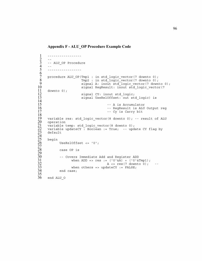
96
Appendix F - ALU_OP Procedure Example Code
-----------------1--2-- ALU_OP Procedure3--4-----------------5
6procedure ALU_OP(Tmp1 : in std_logic_vector(7 downto 0);7
Tmp2 : in std_logic_vector(7 downto 0);8signal A: inout std_logic_vector(7 downto 0);9signal RegResult: inout std_logic_vector(710
downto 0);11signal CY: inout std_logic;12signal UseRelOffset: out std_logic) is13
14-- A is Accumulator15-- RegResult is ALU Output reg16-- Cy is Carry bit17
18variable res: std_logic_vector(8 downto 0); -- result of ALU19operation20variable temp: std_logic_vector(8 downto 0);21variable updateCY : Boolean := True; -- update CY flag by22default23
24begin25
UseRelOffset <= '0';2627
case OP is2829
-- Covers Immediate Add and Register ADD30when ADD => res := ('0'&A) + ('0'&Tmp1);31
A <= res(7 downto 0); --32when others => updateCY := FALSE;33
end case;3435
end ALU_O36

97
1