design guide - americas
TRANSCRIPT

RD162-DGUIDE-01
2020-03-10 Rev.11
1 / 20 © 2020 Toshiba Electronic Devices & Storage Corporation
Overview This Design Guide (hereinafter referred to as this guide) describes designing ultrasonic distance
sensors using a low-noise op-amp TC75S67TU. Ultrasonic distance sensors measure the round trip time until the transmitted ultrasonic wave is reflected by the object and returned, and calculate the distance. This guide describes TC75S67TU applied circuit designs, using an ultrasonic distance sensor integrated with transmitter and receiver as an example.
Application Circuit of Low Noise Op-Amp TC75S67TU
for Ultrasonic Distance Sensor
Design guide
RD162-DGUIDE-01

RD162-DGUIDE-01
2020-03-10 Rev.11
2 / 20 © 2020 Toshiba Electronic Devices & Storage Corporation
Table of Contents
1. Introduction ................................................................ 3
2. Circuit Design .............................................................. 4
2.1. About Low-noise Op-amp TC75S67TU .................................................... 4
2.2. Ultrasonic Transducer C4016A1 .............................................................. 5
2.3. Ultrasonic Distance Sensor Specifications ............................................... 7
2.4. Circuit Design of the Ultrasonic Distance Sensor ..................................... 8
3. Board Design ............................................................. 15
3.1. Example of Board Pattern ..................................................................... 15
3.2. Key Care about on Board Design .......................................................... 16
4. Product Overview ...................................................... 18
4.1. TC75S67TU .......................................................................................... 18
4.2. Pin Description ..................................................................................... 19

RD162-DGUIDE-01
2020-03-10 Rev.11
3 / 20 © 2020 Toshiba Electronic Devices & Storage Corporation
1. Introduction Op-amps are still used in a variety of situations even today in the digital age, and a particularly
important application is their use in a variety of sensors. There are various types of information that can be obtained from nature, such as sound and light,
and there are various types of sensor elements accordingly. Generally, the output signal from a sensor element is very weak, and it is hard to handle as it is, so in most cases it is amplified and processed.
Op-amps are used for this amplification. In addition to amplification, op-amps are used for filters and I-V conversion in various sensors, and it is not an overstatement to say that most modern electronic devices cannot be realized without an op-amp.
Noise characteristics are important in applications with these sensors. If the op-amp itself is noisy, critical sensor signals may be masked by noise, resulting in a decrease in detection sensitivity or false detection, preventing the desired sensing performance from being attained. Therefore, the operational amplifiers used in such applications require low noise levels.
In order to meet these requirements, Toshiba have developed an operational amplifier TC75S67TU with a low noise level of 6 nV/√Hz (@f=1 kHz, GV=40 dB, typical).
This guide describes designing ultrasonic distance sensors using TC75S67TU. For more information on TC75S67TU, refer to the data sheet of the link destination below.
→ TC75S67TU datasheet from here
Click Here

RD162-DGUIDE-01
2020-03-10 Rev.11
4 / 20 © 2020 Toshiba Electronic Devices & Storage Corporation
2. Circuit Design 2.1. About Low-noise Op-amp TC75S67TU
The low-noise op-amp TC75S67TU used in the ultrasonic distance sensors described in this guide took measures from both the circuits and manufacturing processes, and succeeded in reducing the noise level to a greater extent than our existing products.
Generally, noise has 2 ways on the frequency component contained point of view: 1. 1/f noise which is distributed in the low frequency region 2. White noise which is distributed in the wide region from low frequency to high frequency.
TC75S67TU realizes low noise levels such as 16 nV/√Hz (@f=10 Hz) in the low frequency region where 1/f noise is mainly used, and 6 nV/√Hz (@f=1 kHz, typ.) in the region where white noise is mainly used. Fig. 2.1 shows a graph comparing the noise level-frequency characteristics of TC75S67TU and our existing product.
Fig. 2.1 TC75S67TU Input-Converted Noise Voltage-Frequency Characteristics
As shown in Fig. 2.1, the noise of TC75S67TU is greatly improved compared to existing products, making it an optimum op-amp for amplifying the signal of sensors that handle weak signals. In addition to this noise characteristic, TC75S67TU has a very small input bias current of 1 pA, and the offset voltage is also small.
For sensors that handle weak signals, the effect of the offset voltage is also large, which may cause deterioration of the sensor performance. Therefore, a resistor for offset correction may be required at the input terminals. Since the resistor generates thermal noise, the noise may deteriorate in this case. However, since the offset voltage is small for TC75S67TU, it is not necessary to add a resistor for offset compensation. By using TC75S67TU with the above features, high-sensitivity and high-performance sensors can be designed. Please also refer to the application notes below for more information on TC75S67TU noise.
To download the application notes on TC75S67TU noise →
VDD=5 V VSS=GND Ta=25 °C
Equi
vale
nt I
nput
N
oise
Vol
tage
(n
v/√H
z)
Frequency (Hz)
TC75S67TU
Our existing product
Click Here

RD162-DGUIDE-01
2020-03-10 Rev.11
5 / 20 © 2020 Toshiba Electronic Devices & Storage Corporation
2.2. Ultrasonic Transducer C4016A1 Ultrasonic distance sensor integrated with transmitter and receiver for distance measurement,
generally called ultrasonic transducers, consist of a transducer and a resonator. Fig. 2.2 shows a schematic diagram of the ultrasonic distance sensor integrated transmitter and receiver.
Fig. 2.2 Schematic Diagram of the Ultrasonic Transducer
Since transmitter and receiver are integrated, the transducer input and output terminals are common. In the actual circuit, a diode is inserted to separate the transmitting side (the side where the driving pulse is input) from the receiving side (the side where the receiving signal is output). However, this figure is omitted.
Piezoelectric elements such as piezoelectric ceramics, which generate mechanical displacement depending on the magnitude of the applied voltage or, conversely, voltage due to mechanical force, are used for the vibrator.
During transmission, AC pulse voltage is applied to the transducer and the generated vibration is resonated by the resonator to generate and transmit ultrasonic waves. During reception, the vibration is generated by an external ultrasonic wave with a resonator, which is converted into an electrical signal by the vibrator and output. The frequency of the ultrasonic wave used for sensing is determined by the resonance frequency of the resonator. Ultrasonic transducer used in this guide the resonant frequency of C4016A1 made by Nippon Ceramic is 40 kHz.
Fig. 2.3 shows the outline of the ultrasonic transducer C4016A1.
Fig. 2.3 Ultrasonic Transducer (C4016A1 made by Nippon Ceramic)
Transducer (Piezoelectric element)
Resonator
Transmitted wave Received waves
Receive output
Pulse signal for driving the oscillator

RD162-DGUIDE-01
2020-03-10 Rev.11
6 / 20 © 2020 Toshiba Electronic Devices & Storage Corporation
Fig. 2.4 shows C4016A1 transmission operation waveforms. This is the result of observing the drive pulse waveform output from a Microcontroller (this guide uses Arduino) and the waveform of the input/output terminal of the ultrasonic sensor C4016A1. Because of the integrated transmitter and receiver type, the input and output terminals of C4016A1 receive the transmitted ultrasonic signals and their reverberation.
Fig. 2.4 Ultrasonic Sensor Transmission Operation Waveform
In this example, stable operation is started immediately after the driving pulse is input. However, as described above, the ultrasonic sensor operates by resonance, so it may be necessary to apply multiple 40 kHz pulses to transmit ultrasonic waves. Determine the applied wave number of the pulse after confirming it with the actual device.
In the distance sensor using ultrasonic waves, the time (propagation time) between the ultrasonic waves transmitted from the sensor going to the object and reflecting back is measured, and the distance is calculated by the following equation:
𝐷𝐷=𝑣𝑣 × 𝑡𝑡
2 ・・・・ (2.1)
D: Distance (m), v: Sound velocity (m/s), t: Propagation time (s)
The speed of the ultrasonic wave (speed of sound) varies with temperature, but it is about 340 m/s at a temperature of 15 °C. The propagation time is divided by 2 because the ultrasonic wave is the time to go back and forth with the object to be measured.
Since the transmitter and receiver of the integrated ultrasonic sensor are housed in one package, the transmitter receives the reverberation of the transmitted waves in the package even after completion of transmission, as shown in Fig. 2.4. Therefore, there is a lower limit to the detectable distance. About 40 cm is the shortest detection distance for the one used in this guide. If you wish to measure the distance below this, use ultrasonic distance sensor that has separate transmitter and receiver.
Connector Pulse Terminal Waveforms (5 V/div) Drive Pulses Output from the Arduino
C4016A1 I/O Pin Waveforms (2 V/div) Ultrasonic waveforms received by C4016A1
Time axis: 100 μs/div
Receive reverberation
Receive transmitted waves

RD162-DGUIDE-01
2020-03-10 Rev.11
7 / 20 © 2020 Toshiba Electronic Devices & Storage Corporation
This guide uses an Arduino Microcontroller that can control the operation of the entire range sensor and display the measurement results. If you prepare the software, you can use any other type of microcontroller. However, check the operation thoroughly.
2.3. Ultrasonic Distance Sensor Specifications Table 2.1 lists the specifications of this ultrasonic distance sensor circuit.
Table 2.1 Ultrasonic Distance Sensor Specifications
Item Specifications I/F Arduino connections
Control method Control from Arduino and Shield Connected PCs Power supply voltage 5 V from Arduino and Shield board Measurement distance 40 cm~6 m
Onboard ultrasonic sensor Nippon Ceramic C4016A1,
Integrated transmitter and receiver Measured ultrasonic frequency 40 kHz Onboard operational amplifier Toshiba Device & Storage TC75S67TU
RD162-DGUIDE-01
2020-03-10 Rev.11
8 / 20 © 2020 Toshiba Electronic Devices & Storage Corporation
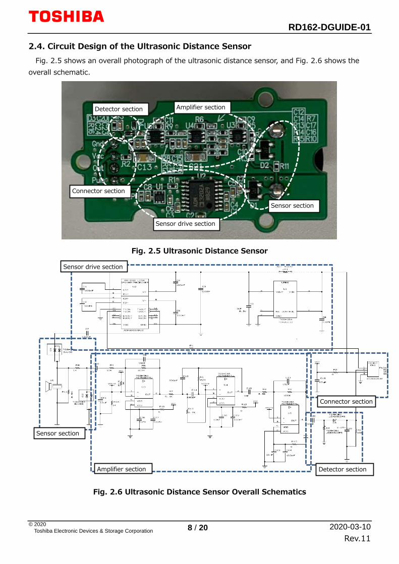
2.4. Circuit Design of the Ultrasonic Distance Sensor Fig. 2.5 shows an overall photograph of the ultrasonic distance sensor, and Fig. 2.6 shows the
overall schematic.
Fig. 2.5 Ultrasonic Distance Sensor
Fig. 2.6 Ultrasonic Distance Sensor Overall Schematics
Amplifier section Detector section
Connector section
Sensor section
Sensor drive section
Sensor section
Sensor drive section
Connector section
Detector section Amplifier section

RD162-DGUIDE-01
2020-03-10 Rev.11
9 / 20 © 2020 Toshiba Electronic Devices & Storage Corporation
This sensor consists entirely of one board. This section describes the circuit operation and settings for each part enclosed by the dotted lines. Fig. 2.7 shows the connector section. Arduino Shield board interface (I/F) connects to the connector.
Fig. 2.7 Connector Section
A 40 kHz burst pulse voltage for resonating the ultrasonic distance sensor is supplied to Pulse terminal, and a 5 V DC voltage is supplied to the VCC terminal from Arduino. C13 is a bypass capacitor that removes the noise ripple superimposed on the power supply. In the board example in this guide, jumpers R2 are arranged so that a resistor can be mounted to configure low-pass filter (LPF) with C13 when low-frequency noise of the power supply is a concern.
On the other hand, signals received by ultrasonic sensors are amplified and output to Arduino from the OUT terminals.
To TCR2EF33 VIN in the sensor drive section
To VCC of other section
To ADM3202 T2IN input in the sensor drive section
From the detector section

RD162-DGUIDE-01
2020-03-10 Rev.11
10 / 20 © 2020 Toshiba Electronic Devices & Storage Corporation
Fig. 2.8 shows the sensor drive section using ANALOG DEVICES's ADM3202 for the interface ICs for EIA-232.
Fig. 2.8 Sensor Drive Section
The resonance pulse supplied from Arduino is a pulse signal that amplitudes between the power supply and GND. However, in order to cause resonance at the ultrasonic sensor C4016A1, the pulse must be amplified at ± around the GND, and ADM3202 is used to convert the signal. This IC has a built-in charge-pump booster and inverter circuits that can output a 12 Vp-p AC pulsed voltage amplifying at ± voltage. To prevent current and voltage fluctuations in the charge pump circuit from affecting other circuits through VCC line, ADM3202 power supply is supplied with 3.3 V from our LDO regulator TCR2EE33.
Through the connector VCC terminal
Through the connector pulse terminal
To ultrasonic sensor

RD162-DGUIDE-01
2020-03-10 Rev.11
11 / 20 © 2020 Toshiba Electronic Devices & Storage Corporation
Fig. 2.9 shows the circuitry around the sensor section.
Fig. 2.9 Sensor Section
D1 and D2 are our switching-diode BAV99. Because the ultrasonic sensor C4016A1 used here is integrated with transmission and reception, the sensor drive must be separated when ultrasonic waves are received, and D1 works this function. On the other hand, the D2 limits the amplitude of the signal that goes around the receiving signal amplifier side during ultrasonic transmission to a diode forward voltage (approx. 0.6 V) or less.
From ADM3202 T2OUT in the sensor drive section
To the amplifier section

RD162-DGUIDE-01
2020-03-10 Rev.11
12 / 20 © 2020 Toshiba Electronic Devices & Storage Corporation
Fig. 2.10 shows the amplifier section of the signal received by the ultrasonic sensor.
Fig. 2.10 Amplifier Section
From the level of the reflected signal at the maximum measurement distance (6 m), you should amplify about 70 dB in this section. In addition, since the open-loop gain of TC75S67TU at 40 kHz is approximately 40 dB, the gain of each stage is set to 30 dB or less in view of the allowance, and a three-stage configuration is adopted in which three TC75S67TU are used. Both of the operational amplifiers U3, U4, and U6 are DC biased to a voltage (mid-point voltage) of VCC/2 obtained by dividing the power supply voltage with R14 and R15, and the signal amplitudes at VCC/2 center.
Since the inputs of each stage do not need to be high impedance and the supply of the mid-point bias voltage can be simplified and the number of components can be reduced, both are inverting amplifiers. Each stage of the op-amp also consists of a filter that filters out unwanted frequency-domain signals.
The first-stage op-amp (U3) uses R5 and C9 to form a primary LPF to eliminate unwanted high-frequency components. Also, if the feedback resistance is too large, the effect of thermal noise increases. Therefore, the feedback resistor R5 is set to 160 kΩ and the gain here is set to 24.1 dB.
The equations and setting values for the cutoff frequency fC1 and gain (GV1) are as follows.
𝑓𝑓𝐶𝐶1=1
2 × 𝜋𝜋 × 𝑅𝑅5 × 𝐶𝐶9=
12 × 𝜋𝜋 × 160 × 103 × 10 × 10−12
≅ 99.5 𝑘𝑘𝐻𝐻𝑍𝑍 ・・・・ (2.2)
R5: 160 kΩ, C9: 10 pF
𝐺𝐺𝑣𝑣1=−𝑅𝑅5𝑅𝑅4=−
160 × 103
10 × 103=ー16 (24 𝑑𝑑𝑑𝑑) ・・・・ (2.3)
R4: 10 kΩ, R5: 160 kΩ
From the ultrasonic sensor
To the detector section

RD162-DGUIDE-01
2020-03-10 Rev.11
13 / 20 © 2020 Toshiba Electronic Devices & Storage Corporation
The second-stage o-amp (U4) has a 40 kHz quadratic multiple feedback bandpass filter (BPF) to remove unnecessary components other than the received signal. This BPF has a quality factor (Q) of 3.4 so the gain at the center frequency of the BPF is reduced to 18 dB considering of peaking.
The center frequency (f0) of the BPFs, the gain (GV2) in f0, and the equation and setting values for the Q are shown below.
𝑓𝑓0=1
2 × 𝜋𝜋� 𝑅𝑅7+𝑅𝑅13𝐶𝐶12 × 𝐶𝐶14 × 𝑅𝑅7 × 𝑅𝑅13 × 𝑅𝑅6
=1
2 × 𝜋𝜋� 5.1 × 10³+2.7 × 10³
330 × 10−12 × 330 × 10−12 × 5.1 × 103 × 2.7 × 103 × 82 × 103≅ 40.1 𝑘𝑘𝐻𝐻𝑘𝑘 ・・・ (2.4)
R7: 5.1 kΩ, R13: 2.7 kΩ, R6: 82 kΩ, C12: 330 pF, C14: 330 pF
𝐺𝐺𝑣𝑣2=−𝐶𝐶14 × 𝑅𝑅6
(𝐶𝐶12 + 𝐶𝐶14) × 𝑅𝑅7=−
330 × 10−12 × 82 × 103
(330 × 10−12 + 330 × 10−12) × 5.1 × 103≅ −8 (18 𝑑𝑑𝑑𝑑) ・・・ (2.5)
R6: 82 kΩ, R7: 5.1 kΩ, C12: 330 pF, C14: 330 pF
𝑄𝑄=12�𝑅𝑅6 × �
1𝑅𝑅7
+1𝑅𝑅13
� =12
× �82 × 103 × �1
5.1 × 10³+
12.7 × 10³
� ≅ 3.4 ・・・ (2.6)
R6: 82 kΩ, R7: 5.1 kΩ, R13: 2.7 kΩ
The third-stage op-amp (U6) also has LPF configurations with C11 and R9. Though the gain is determined by R8 and R9, the gain at this stage is set to 30 dB to compensate for the lack of gain for the entire three stages.
The equations and setting values for the cutoff frequency (fC3) and amplification factor (GV3) are as follows.
𝑓𝑓𝐶𝐶3=1
2 × 𝜋𝜋 × 𝑅𝑅9 × 𝐶𝐶11=
12 × 𝜋𝜋 × 100 × 103 × 15 × 10−12
≅ 106.2 𝑘𝑘𝐻𝐻𝑍𝑍 ・・・・ (2.7)
R9: 100 kΩ, C11: 15 pF
𝐺𝐺𝑣𝑣3=−𝑅𝑅9𝑅𝑅8=−
100 × 103
3.3 × 10³≅ −30 (30 𝑑𝑑𝑑𝑑) ・・・・ (2.8)
R8: 3.3 kΩ, R9: 100 kΩ,
The overall gain of the three stages is 16 times x8 times x30 times = 3840 times (approx. 72 dB). Two types of capacitors, 100 nF and 10 nF, are connected in parallel to the power supply bypass capacitors of each op-amp. This is to effectively eliminate power supply noises in a wide frequency range by lowering the impedances at lower frequencies below them with large 100 nF capacitors in the high frequency range above 1 MHz with small 10 nF capacitors.
RD162-DGUIDE-01
2020-03-10 Rev.11
14 / 20 © 2020 Toshiba Electronic Devices & Storage Corporation
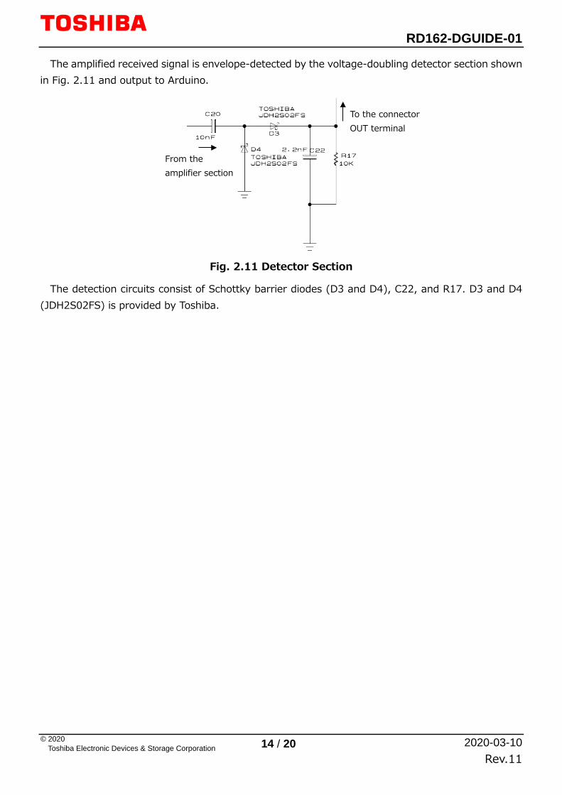
The amplified received signal is envelope-detected by the voltage-doubling detector section shown in Fig. 2.11 and output to Arduino.
Fig. 2.11 Detector Section
The detection circuits consist of Schottky barrier diodes (D3 and D4), C22, and R17. D3 and D4 (JDH2S02FS) is provided by Toshiba.
From the amplifier section
To the connector OUT terminal

RD162-DGUIDE-01
2020-03-10 Rev.11
15 / 20 © 2020 Toshiba Electronic Devices & Storage Corporation
3. Board Design 3.1. Example of Board Pattern This board uses both front and back two-layer boards. Fig. 3.1 shows the board pattern on the top side (component mounting surface) and Fig. 3.2 shows the board pattern on the bottom side. Note on the Fig. 3.1 and 3.2 show key care about. Section 3.2 shows for more detail.
Fig. 3.1 Board Pattern (Top Side)
Fig. 3.2 Board Pattern (Bottom Side)
③ Thermal treatment ③ Thermal treatment
② Return current
④ Impedance reduction
Consideration of heat
Consideration of heat
Consideration of heat
Consideration of heat
③ Thermal treatment
③ Thermal treatment Consideratio
n of heat ① Separation and 1-
point connection of each part GND
Tear drop ⑤ Tear drop
Amplifier and detector section
side
⑥ Bypass capacitor
Tear drop ⑤ Tear drop ⑥ Power line
⑥ Bypass capacitor
⑤ Tear drop ⑥ Bypass capacitor
⑤ Tear drop Sensor Drive Side
③Thermal treatment ③Thermal treatment
④ Impedance reduction
③ Thermal treatment

RD162-DGUIDE-01
2020-03-10 Rev.11
16 / 20 © 2020 Toshiba Electronic Devices & Storage Corporation
3.2. Key Care about on Board Design ① Separation and 1-point connection of each part GND (see Fig. 3.1)
Separate the GND of the ultrasonic sensor drive unit side and the receiving signal amplification and detection unit side and connect them to one point. In the example of the pattern shown in Fig. 3.1, each terminal is separated as solid GND, and only the GND terminal of connector No. 4 is connected at one point. This is to prevent voltage and current fluctuations caused by the operation of ADM3202 charge pumps in the ultrasonic sensor drive from entering the received signal amplification circuits that amplify minute signals.
② Return current (see Fig. 3.2) When transmitting ultrasonic waves, the current (return current) returning from the ultrasonic
sensor C4016A1 to ADM3202 should be directly returned to the drive in a low-impedance path and should not flow into the GNDs of the received signal amplifiers. ADM3202 outputs a boosted large-amplitude signal, and the return current contains the voltage and current fluctuation components due to it. If the voltage and current fluctuations flow through the GND of the receiving signal amplifier, there may be adverse effects such as noises.
In the pattern example in this guide, the wiring impedance is lowered by making the width thicker, and the wiring impedance is returned directly from the GND terminal of the ultrasonic sensor to the drive side of the ultrasonic sensor.
Current always flows in a closed loop. Therefore, provide the IC for driving the IC → Ultrasonic Sensor → Ultrasonic Sensor GND → Drive ICs and the path through which the current returns so that the effect on other parts is minimized.
③ Thermal treatment In the example of the pattern, "Thermal treatment" is indicated by a cross or T-shape in the
wiring from each pad to GND so that heat does not escape to a wide solid GND during soldering. This is to prevent the parts from overheating and deteriorating or breaking due to the heat escaping and the longer soldering time. Usually, the cross and T-shaped layout sections are buried in the solder after soldering, making it impossible to visually see them.
④ Impedance reduction For a two-layer board, provide as many vias as possible between the front and back of the
board to reduce the impedance between the front and back surfaces. This reduces the impedance of the entire GND and enhances the solid GND reference to prevent potential differences from occurring in the area and to prevent noise from spreading.
⑤ Land teardrop shape (see Fig. 3.1) In this example, the land and pad-to-wire connections are broadened to provide a tear drop
(tear drop) configuration. This is intended to prevent the generation of singularities in the current at the pad area and to increase the connection strength between the pad and the wiring.
⑥ Bypass Capacitor Location (see Fig. 3.1) To eliminate the noise superimposed on the power supply voltage line, connect two bypass
capacitors (100 nF and 10 nF) of the op-amp as close as possible to the power supply voltage pin of the corresponding device and to the power supply line side.
Please select a capacitor with as small an ESR as possible. ESR=1 Ω or less is recommended.

RD162-DGUIDE-01
2020-03-10 Rev.11
17 / 20 © 2020 Toshiba Electronic Devices & Storage Corporation
⑦ Guard ring Though not included in the pattern example in this guide, it is recommended to provide a
guard ring around the area that handles minute signals if you are concerned about noise jumping into the op-amp's input. The guard ring prevents noise, etc. from entering the input terminal from other wiring due to the line-to-line capacitance or stray capacitance, and also prevents leakage current from flowing due to the generation of a potential.
As for the guard ring, in order to prevent noise from flying out as a loop antenna, a cut may be inserted halfway, but the presence or absence of the cut should be judged by experiments on the actual board, etc. If no cuts are inserted, make the area surrounding it as small as possible to reduce the magnetic flux passing through the loop.

RD162-DGUIDE-01
2020-03-10 Rev.11
18 / 20 © 2020 Toshiba Electronic Devices & Storage Corporation
4. Product Overview 4.1. TC75S67TU
• Low Equivalent Output Noise Voltage: VNI=16 nV/√Hz (typ.) @f=10 Hz, RS=100 Ω, Rf=10 kΩ, VDD=2.5 V, VSS=GND, GV=40 dB VNI=6 nV/√Hz (typ.) @f=1 kHz, RS=100 Ω, Rf=10 kΩ, VDD=2.5 V, VSS=GND, GV=40 dB
• Low-input-bias current: II = 1 pA (typ.) • Low supply current: IDD = 430 μA (typ.) @VDD=2.5 V, VSS = GND • Low power supply voltage drive: VDD, VSS=2.2 to 5.5 V
Fig. 4.1 Equivalent output Noise Fig. 4.2 Phase Margin & Gain
Fig.4.3 External View and Pin Assignment Fig.4.4 Dimensions
Refer to the data sheet for details of each characteristic.
To download the datasheet for TC75S67TU →
Click Here

RD162-DGUIDE-01
2020-03-10 Rev.11
19 / 20 © 2020 Toshiba Electronic Devices & Storage Corporation
4.2. Pin Description Table 4.1 TC75S67TU Pin Descriptions
Pin number
Pin name Function
1 IN (+) Non-inverting input pin
2 VSS Connect this pin to GND when using a single power supply with a negative power supply terminal.
3 IN (-) Inverting input terminal 4 OUT Output terminal
5 VDD
The maximum rating for use with a single power supply with a positive power supply terminal is 6 V. For stable operation, it is recommended to use a bypass capacitor of 0.1 μF and a capacitor of 0.01 μF or more (ESR=1 Ω or less).

RD162-DGUIDE-01
2020-03-10 Rev.11
20 / 20 © 2020 Toshiba Electronic Devices & Storage Corporation
Terms of Use This terms of use is made between Toshiba Electronic Devices and Storage Corporation (“We”) and customers who
use documents and data that are consulted to design electronics applications on which our semiconductor devices are mounted (“this Reference Design”). Customers shall comply with this terms of use. Please note that it is assumed that customers agree to any and all this terms of use if customers download this Reference Design. We may, at its sole and exclusive discretion, change, alter, modify, add, and/or remove any part of this terms of use at any time without any prior notice. We may terminate this terms of use at any time and for any reason. Upon termination of this terms of use, customers shall destroy this Reference Design. In the event of any breach thereof by customers, customers shall destroy this Reference Design, and furnish us a written confirmation to prove such destruction. 1. Restrictions on usage 1. This Reference Design is provided solely as reference data for designing electronics applications. Customers shall
not use this Reference Design for any other purpose, including without limitation, verification of reliability. 2. This Reference Design is for customer's own use and not for sale, lease or other transfer. 3. Customers shall not use this Reference Design for evaluation in high or low temperature, high humidity, or high
electromagnetic environments. 4. This Reference Design shall not be used for or incorporated into any products or systems whose manufacture,
use, or sale is prohibited under any applicable laws or regulations. 2. Limitations 1. We reserve the right to make changes to this Reference Design without notice. 2. This Reference Design should be treated as a reference only. We are not responsible for any incorrect or
incomplete data and information. 3. Semiconductor devices can malfunction or fail. When designing electronics applications by referring to this
Reference Design, customers are responsible for complying with safety standards and for providing adequate designs and safeguards for their hardware, software and systems which minimize risk and avoid situations in which a malfunction or failure of semiconductor devices could cause loss of human life, bodily injury or damage to property, including data loss or corruption. Customers must also refer to and comply with the latest versions of all relevant our information, including without limitation, specifications, data sheets and application notes for semiconductor devices, as well as the precautions and conditions set forth in the "Semiconductor Reliability Handbook". 4. When designing electronics applications by referring to this Reference Design, customers must evaluate the whole
system adequately. Customers are solely responsible for all aspects of their own product design or applications. WE ASSUME NO LIABILITY FOR CUSTOMERS' PRODUCT DESIGN OR APPLICATIONS. 5. No responsibility is assumed by us for any infringement of patents or any other intellectual property rights of
third parties that may result from the use of this Reference Design. No license to any intellectual property right is granted by this terms of use, whether express or implied, by estoppel or otherwise. 6. THIS REFERENCE DESIGN IS PROVIDED "AS IS". WE (a) ASSUME NO LIABILITY WHATSOEVER, INCLUDING
WITHOUT LIMITATION, INDIRECT, CONSEQUENTIAL, SPECIAL, OR INCIDENTAL DAMAGES OR LOSS, INCLUDING WITHOUT LIMITATION, LOSS OF PROFITS, LOSS OF OPPORTUNITIES, BUSINESS INTERRUPTION AND LOSS OF DATA, AND (b) DISCLAIM ANY AND ALL EXPRESS OR IMPLIED WARRANTIES AND CONDITIONS RELATED TO THIS REFERENCE DESIGN, INCLUDING WARRANTIES OR CONDITIONS OF MERCHANTABILITY, FITNESS FOR A PARTICULAR PURPOSE, ACCURACY OF INFORMATION, OR NONINFRINGEMENT. 3. Export Control Customers shall not use or otherwise make available this Reference Design for any military purposes, including
without limitation, for the design, development, use, stockpiling or manufacturing of nuclear, chemical, or biological weapons or missile technology products (mass destruction weapons). This Reference Design may be controlled under the applicable export laws and regulations including, without limitation, the Japanese Foreign Exchange and Foreign Trade Law and the U.S. Export Administration Regulations. Export and re-export of this Reference Design are strictly prohibited except in compliance with all applicable export laws and regulations. 4. Governing Laws This terms of use shall be governed and construed by laws of Japan.