design & fabrication of a high-voltage photovoltaic cell ... · design & fabrication of a...
TRANSCRIPT

Design & Fabrication of a High-Voltage Photovoltaic Cell
Jennifer Felder
Office of Science, Science Undergraduate Laboratory Internship (SULI)
North Carolina State University
SLAC National Accelerator Laboratory
Menlo Park, CA
12 August 2011
Prepared in partial fulfillment of the requirements of the Office of Science, Department of
Energy’s Science Undergraduate Laboratory Internship under the direction of Chris Kenney
at the Particle Physics and Astrophysics (PPA) Division of SLAC National Accelerator
Laboratory.
Participant:
Signature
Research Advisor:
Signature

TABLE OF CONTENTS
Abstract ii
Introduction 1
Methods 3
Results 7
Discussion 8
Conclusion 10
Acknowledgments 10
References 11
i

ABSTRACT
Design & Fabrication of a High-Voltage Photovoltaic Cell. JENNIFER FELDER (North
Carolina State University, Raleigh, NC 27615) CHRIS KENNEY (Particle Physics and As-
trophysics (PPA) Division of SLAC National Accelerator Laboratory, Menlo Park, CA 94025)
Silicon photovoltaic (PV) cells are alternative energy sources that are important in sus-tainable power generation. Currently, applications of PV cells are limited by the low outputvoltage and somewhat low efficiency of such devices. In light of this fact, this project inves-tigates the possibility of fabricating high-voltage PV cells on float-zone silicon wafers havingoutput voltages ranging from 50 V to 2000 V. Three designs with different geometries ofdiffusion layers were simulated and compared in terms of metal coverage, recombination,built-in potential, and conduction current density. One design was then chosen and opti-mized to be implemented in the final device design. The results of the simulation serve as afeasibility test for the design concept and provide supportive evidence of the effectiveness ofsilicon PV cells as high-voltage power supplies.
ii

INTRODUCTION
Background Information
Solar photovoltaic (PV) energy is produced by converting light energy to electrical en-
ergy. The energy of light, composed of photons, is determined by the color and therefore
frequency of that light. As explained by the photoelectric effect, when the energy of that
light is high enough, it excites the electrons on the surface of a material, causing them to
move to a higher energy level. While in normal materials these excited electrons return
to their original state relatively quickly, in photovoltaic devices these excited electrons are
driven to create a current; this is known as the photovoltaic effect. The electrons do not
return to their lower energy state because of an asymmetry that is inherent to this type of
materials, and a potential difference is created. PV cells are developed to take advantage of
this effect, and thus have a unique functionality: they conduct as diodes in a dark environ-
ment and in light they gain a charge, producing a photovoltage. [1]
One distinguishing feature of the PV device designed in this project is that it is fabri-
cated on float-zone silicon wafers. There are two processes typically used to fabricate silicon
wafers, namely the float-zone and Czochralski methods. Both processes extract a single
crystal as the final product; however, the Czochralski does so using a melt from which the
crystal is extracted directly, while the float-zone technique passes a liquid phase through a
polycrystalline rod. Using the float-zone method provides several advantages, in particular
the fact that the wafers have fewer impurities, which improves the performance of the final
device. However, there also exists a tradeoff in using this method: the wafers are much more
expensive than those prepared using other methods. [1]
This PV device also has a comparative advantage in terms of efficiency, as a result
of the application for which it was developed. The device was designed to act as a power
source for the Enriched Xenon Observatory (EXO) experiment. The thickness of the ma-
1

terial, surrounding temperature, and wavelength of the incident light all contribute to the
efficiency of a PV device. Because the environment of the experiment is known and rela-
tively constant, the surrounding temperature and wavelength of the light to be converted to
electrical energy is known. The PV cell can therefore be designed to absorb light near the
peak in its absorption spectrum, increasing the efficiency of the device.
Prior Work: Silicon Solar Cells in the Past Decade
In the past decade in particular, efforts have been made to significantly increase the
efficiency, and therefore utility, of PV devices. A twenty-four percent efficient silicon solar
cell was achieved by altering the design of such cells in several ways. First, the silicon cell
was covered in a layer of SiO2; this reduced the recombination losses at the surface of the
cell covered in oxide. Second, the surface was textured with an inverted pyramid pattern,
reducing external light reflection of the top cell surface and increasing the internal light
reflection of the rear cell surface. This increased the ability of the cell to absorb infrared
light. Finally, the addition of a double layer antireflection coat composed of a MgF2/ZnS
compound decreased the reflective losses of the cell. [2]
Another promising advance in this area of research was made by using an alternate
texturing pattern on the cell surface. Instead of the previously described inverted pyramid
scheme, cells have also been fabricated with a honeycomb pattern, which consists of wells in
the shape of hemispheres aligned adjacently on the cell surface. This, when combined with
the previously described technique of covering the cell in oxide, increased the efficiency of
monocrystalline cells from 24.0% to 24.4% and of multicrystalline cells from 18.6% to 19.8%.
The symmetric pattern, while reducing the angle and height of surface features, allowed
for more internal reflection; more light was absorbed by the cell, increasing its efficiency at
wavelengths that are more difficult for PV devices to absorb. [3]
2

Motivation & Purpose
While solar cells have been fabricated with success for some time, their applications are
still limited. These limiting factors include the low output voltage and somewhat low effi-
ciency typical PV devices yield. This project aims to explore producing a single PV device
having an output voltage up to 2000 V. Such a high-voltage DC power supply could sub-
stantially improve the utility of renewable energy sources such as silicon solar cells.
This high-voltage PV device was designed to be a power source for the EXO experi-
ment. The goal of this experiment is to use the 136 isotope of Xenon to observe neutrinoless
double beta decay. While it has not yet been observed, being able to observe this process
would lead to two major discoveries: discerning whether the neutrino is its own antiparticle
and measuring the half-life of the neutrinoless double-beta decay process, which would help
in estimating the mass of the neutrino. The experiment also has importance in improving
the current limit on the neutrino mass estimate. [4]
METHODS
Design Process
In beginning the mask design process, a list of features necessary for the PV cell was first
developed. These features included both fabrication test features and device features. The
purpose of the fabrication tests included in the design was to verify the functionality of the
following aspects of the device: the conductivity of the metal, the conductivity of the N and
P diffusion layers, the contact between both the metal and N diffusion layer and the metal
and P diffusion layer, diode functionality, trench hopping and the field oxide etch and glass
etch patterns. Each of these aspects required a separate fabrication feature, as this allows
the various properties of the device to be tested independently of one another. In this way,
if the final PV cell does not work properly after fabrication, it will be relatively easier to
3

determine the failing feature and to diagnose and fix the problem.
Once the fabrication test features were designed, the design of the actual PV device
was developed. High voltage PV cells were designed having dimensions of both 50 µm
and 100 µm per side. Three main cell designs were developed for the mask, each having
a different geometry of the diffusion layers; these designs for the 100 µm square cell are
included in Figure 1. In this figure, the bright green layer is the field oxide (trench) etch
pattern, the orange is the diffusion-to-metal contact, the light green is the N-type diffusion,
and the pink is the P-type diffusion layer. Different devices were designed to produce various
output voltages ranging from 50 V to 2000 V. To determine how many cells were needed in
each module for a desired output voltage, several parameters of the silicon PV cells had to
be calculated.
The intrinsic doping concentration, ni, of the substrate, silicon, is known to be ap-
proximately 1010 cm−3, which was included as the theoretical value in Table 3. Next, the
built in potential, φj, of the individual PV cell was calculated using Equations 1 and 2, in
which NA and ND are the active acceptor and donor dopant concentrations respectively, and
VT is the thermal voltage of a material at a specific temperature, in this case of silicon at
300 K.
φj =kT
qln(NAND
n2i
)(1)
VT =kT
q= 0.0259V (2)
Finally, the depletion width, ωdo, of the cell was calculated using Equation 3 and
Equation 4; here εs represents the permittivity of a material, which in this case is silicon,
and q is the charge of an electron.
4

ωdo =
√2εsq
( 1
NA
+1
ND
)φj (3)
εs = εoεr (4)
Table 1 shows the actual variable values used to calculate the parameters of the PV
device. The resulting calculated parameters of the PV device, defined in the formulae above,
were then calculated to produce theoretical results for those cell parameters.
The calculated built-in voltage of the PV cell was used to calculate how many cells
connected in series were needed to produce various output voltages. Each module has a
square geometry; therefore, the next largest perfect square to the number of cells needed
was chosen to determine the size of each module. The number of cells in each PV cell is
summarized in Table 2.
Different layouts of the cells were also considered, including linear, circular, and hexag-
onal designs. Several features were added to the PV device, including the ability to bypass
a particular cell, connections for external switches, and side-entrance photo switches. By-
pass diodes were necessary because of the series connections between individual cells: if one
failed, the entire device may not function. Therefore, adding bypass diodes prevents the
entire device from failing in the event of an individual cell failing. [1]
Simulation Process
The PV device was designed in software first to test the various parameters of the designs
being considered. Three basic designs for the individual PV cells were first simulated; each
had a different geometry of the diffusion layer, matching those in the mask design, with
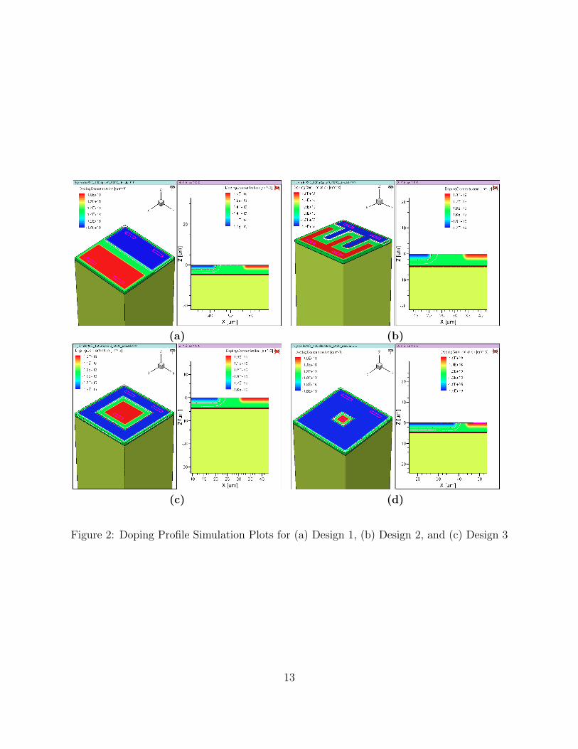
all other parameters being equal. These simulated cell designs are shown in Figure 2. In
5

this figure, dark green layer is the support wafer, light green is the Silicon-On-Insulator
(SOI) layer, red is the N-type diffusion, and blue is the P-type diffusion. The main purpose
of the simulation process was to assess the performance of each design with respect to
a few parameters. The first parameter that was examined was the Shockley-Read Hall
(SRH) recombination. As recombination limits the current generation capability of the cell,
having low recombination is desirable. Another factor of each cell design that was modeled
was the built-in potential. The doping geometry that maximizes the built-in potential is
more advantageous, as it would require fewer individual cells to produce a given voltage,
reducing the size of the overall device. Finally, the conduction current of each design was
also studied, especially in the region between the N-type and P-type diffusion areas. Using
these parameters, the three main designs were compared, to determine which geometry of
the dopants provided optimal performance.
After examining the simulated performance, the design shown in Figure 2(c) was
chosen to be implemented in the actual PV device, and so some parameters were then
adjusted to optimize the performance of that particular design, leading to a fourth cell design.
All of the wafers on which the PV devices were to be fabricated had N-type substrates. For
this reason, any N-type doped layers would simply function as ohmic contacts. Therefore,
the area of P-type dopant was maximized. The minimum area of the N-type dopant and
of the distance between the two dopant types was mainly determined by the limitation in
precision of the alignment equipment used to align the mask to the wafer.
Fabrication Process
This high-voltage PV cell is being fabricated at the Stanford Nanofabrication Facility.
The first step was to remove impurities from and oxidize the wafers on which the PV cells
were to be fabricated. To do so, the wafers went through the following wet-etch procedure.
• 20 minutes in 9:1 H2SO4 : H2O2 mixture; rinsed with deionized water; dried with a
6

spin dryer
• 10 minutes in a 4:1 H2SO4 : H2O2 bath to remove organic particles; deionized water
rinse
• 30 seconds in a 50:1 HF mixture for oxide etching; rinsed with deionized water
• 10 minutes in 5:1:1 H2O:H2O2:HCl bath to remove metal ions; rinsed with deionized
water; cycle through spin dryer
• Oxidation process: WET 850 Tylan process [5]; variable time set to 20 minutes
With the oxidation process complete, there are still several steps that need to be
completed to finish fabricating the device. Thus far, only the first step of the fabrication
process has been completed; device fabrication and testing will be continued in future work.
RESULTS
Three parameters of the individual PV cell were calculated, as previously described;
these calculated values comprise the theoretical results of those cell parameters. These
same properties were measured using the simulation software, to assess the validity of the
calculated values and provide a more extensive theoretical basis on which to judge the final
device. These results are summarized in Table 3. As shown in the table, the calculated and
simulated values agree fairly closely, within a margin of error. This adds credibility both
to the calculations and simulation results. As measuring ωdo directly in the simulation was
only possible by estimating a value off of a plot, Equation 3 was used with the value of φj
measured from the simulation to get a more precise value for comparison.
In addition to the three basic parameters of each cell that were calculated, other
factors of a PV cell are critical to the device performance, yet cannot be easily or directly
7

calculated by hand. For this type of properties, simulation is imperative to comparing
different designs. One such factor is the SRH recombination of the simulated cells. An ideal
PV cell would have minimal recombination, which limits the output current of the cell. The
SRH recombination plots for the various designs are included in Figure 3.
Another property of PV cells that was simulated was the conduction current density.
A functional cell needs conduction between contacts on the N and P diffusion layers; there-
fore the conduction current density is expected to be higher between contacts and minimal
elsewhere. It is also desirable to have higher conduction current on the surface of the cell, as
it is that portion of the device that is designed to be conductive. The plots of the conduction
current density for each design are shown in Figure 5.
To simulate the operation of the cell as a photovoltaic device, several parameters had
to be specified. To effectively simulate the environment in which this device could potentially
operate, the optical generation of the device was set to 1018 cm−3s−1. The diffusion implants
in the actual PV cell are approximately 2 µm deep; assuming a Gaussian distribution with a
peak value of 1019 cm−3 of the diffusion layer, the standard deviation was adjusted to achieve
this in the simulation. Finally, to bias the cell to 0 V, a resistive contact with a value of 105
Ω was connected to the diffusion contacts.
DISCUSSION
Some properties of the individual cells are easier to compare in the mask designs, while
others are more evident in simulation. When designing the mask for the PV cells, enough
metal has to be placed on the cell to provide adequate contact to the diffusion layers, to
create a strong electrical contact. However, the area of the cell covered by metal should be
minimal, as metal prevents light from being absorbed by the cell. Comparing the layout
designs in Figure 1, it is clear that the design in Figure 1(c) has the best performance in
8

minimizing the area of metal coverage.
Several trends emerge from examining the simulation results of the four designs. In
all of the designs the SRH recombination is higher in the area between the two diffusions.
As recombination limits the output of a PV cell, the area with high recombination should
be minimized. The optimized design has the least area between diffusions, and therefore
the most desirable recombination profile, as shown in Figure 3(c). In contrast, the design in
Figure 3(a) shows the greatest amount of recombination in its profile.
The designs were also compared in terms of built-in potential. Comparing the built-in
potential simulation plots for each device in Figure 4, the potential does not vary more than
0.01 V between designs. This is an important factor when comparing cells, as the built-in
potential determines how many cells are needed to produce a given output voltage, which
determines the size of the overall device. However, in this case, the built-in potential for all
designs compared is the nearly same, as expected because the built-in potential is only de-
pendent upon the doping concentrations and intrinsic concentration of the substrate, which
is constant for all devices. This is therefore not a determining factor in choosing a cell design.
Finally, the conduction current density was compared among designs. A higher con-
duction current is expected between diffusion contacts: the current generated in the cell must
flow between the contacts to be an effective power source. As the area of the designs being
compared is constant, the design with the best conduction current density profile can be
assumed to have the most ideal conduction current profile as well. The design in Figure 5(c)
has the most favorable profile; in contrast, Figure 5(a) has the least ideal conduction current
properties.
9
CONCLUSION
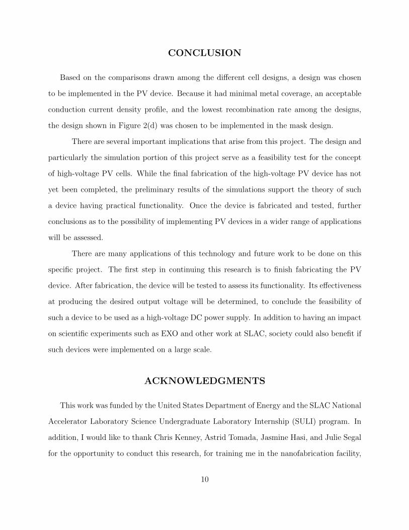
Based on the comparisons drawn among the different cell designs, a design was chosen
to be implemented in the PV device. Because it had minimal metal coverage, an acceptable
conduction current density profile, and the lowest recombination rate among the designs,
the design shown in Figure 2(d) was chosen to be implemented in the mask design.
There are several important implications that arise from this project. The design and
particularly the simulation portion of this project serve as a feasibility test for the concept
of high-voltage PV cells. While the final fabrication of the high-voltage PV device has not
yet been completed, the preliminary results of the simulations support the theory of such
a device having practical functionality. Once the device is fabricated and tested, further
conclusions as to the possibility of implementing PV devices in a wider range of applications
will be assessed.
There are many applications of this technology and future work to be done on this
specific project. The first step in continuing this research is to finish fabricating the PV
device. After fabrication, the device will be tested to assess its functionality. Its effectiveness
at producing the desired output voltage will be determined, to conclude the feasibility of
such a device to be used as a high-voltage DC power supply. In addition to having an impact
on scientific experiments such as EXO and other work at SLAC, society could also benefit if
such devices were implemented on a large scale.
ACKNOWLEDGMENTS
This work was funded by the United States Department of Energy and the SLAC National
Accelerator Laboratory Science Undergraduate Laboratory Internship (SULI) program. In
addition, I would like to thank Chris Kenney, Astrid Tomada, Jasmine Hasi, and Julie Segal
for the opportunity to conduct this research, for training me in the nanofabrication facility,
10

and for helping in many ways throughout the project. Finally, I would like to acknowledge
the contribution of Sentaurus Synopsis simulation software to this project.
REFERENCES
[1] J. Nelson, The Physics of Solar Cells. London: Imperial College Press, 2003. 7 July
2011.
[2] J. Zhao, A. Wang, P. Altermatt, and M. A. Green, “Twenty-four percent efficient
silicon solar cells with double layer reflection coatings and reduced resistance loss,” Applied
Physics Letters, vol. 66, pp. 3636-3638, 26 June 1995.
[3] J. Zhao, A. Wang, M. A. Green, and F. Ferrazza, “19.8% efficient “honeycomb”
textured multicrystalline and 24.4% monocrystalline silicon colar cells,” Applied Physics
Letters, vol. 73, num. 14, pp. 1991-1993, 5 October 1998.
[4] Enriched Xenon Observatory, “EXO: About the Experiment,” 20 August 2010, http:
//www-project.slac.stanford.edu/exo/ .
[5] Stanford Nanofabrication Facility, “WET850 Tylan Recipe,” http://snf.stanford.edu/
Equipment/tylanrecipes/wet/WET850 .
11

FIGURES
(a) (b)
(c)
Figure 1: Mask Design of Individual PV Cells for (a) Design 1, (b) Design 2, and (c) Design3
12
(a) (b)
(c) (d)
Figure 2: Doping Profile Simulation Plots for (a) Design 1, (b) Design 2, and (c) Design 3
13

(a) (b)
(c) (d)
Figure 3: SRH Recombination Simulation Plots for (a) Design 1, (b) Design 2, and (c)Design 3
14

Figure 4: Electrostatic Potential Plots of Design 4, Optimized Design 3
15

(a) (b)
(c) (d)
Figure 5: Conduction Current Density Simulation Plots for (a) Design 1, (b) Design 2, and(c) Design 3
16

TABLES
Parameter Value UnitsNA 2 · 1015 (1019) cm−2 (cm−3)ND 2 · 1015 (1019) cm−2 (cm−3)µn 1300 cm2/V·cmµp 440 cm2/V·cmρ 10 kΩ · cmεr 11.7εo 8.85 · 10−14 F
cm
q 1.609 · 10−19 C
Table 1: Values of Various Parameters Used in the Calculations In Equations 1-6
Output Voltage (V) Cells Needed Sq. Matrix Actual Number Cells50 52 8 x 8 64100 104 11 x 11 121200 207 15 x 15 225500 516 23 x 23 5291000 1,031 33 x 33 1,0892000 2,062 46 x 46 2,116
Table 2: Summary of Cells Needed in PV Cell Modules to Produce Given Output Voltages
Parameter Theoretical Value Simulated Value Unitsni 1.01 · 1010 1.5 · 1010 cm−3
ωdo 0.0166 0.01580 µmφj 1.07 0.970 V
Table 3: Values of Calculated & Simulated Parameters of PV Cell
17