design, fabrication, and characterization of a compact
TRANSCRIPT

Purdue UniversityPurdue e-Pubs
CTRC Research Publications Cooling Technologies Research Center
2019
Design, fabrication, and characterization of acompact hierarchical manifold microchannel heatsink array for two-phase coolingD. BackPurdue University
K. P. DrummondPurdue University
M. D. SinanisPurdue University
J. A. WeibelPurdue University, [email protected]
S V. GarimellaPurdue University, [email protected]
See next page for additional authors
Follow this and additional works at: https://docs.lib.purdue.edu/coolingpubs
This document has been made available through Purdue e-Pubs, a service of the Purdue University Libraries. Please contact [email protected] foradditional information.
Back, D.; Drummond, K. P.; Sinanis, M. D.; Weibel, J. A.; Garimella, S V.; Peroulis, D.; and Janes, D. B., "Design, fabrication, andcharacterization of a compact hierarchical manifold microchannel heat sink array for two-phase cooling" (2019). CTRC ResearchPublications. Paper 346.http://dx.doi.org/10.1109/TCPMT.2019.2899648

AuthorsD. Back, K. P. Drummond, M. D. Sinanis, J. A. Weibel, S V. Garimella, D. Peroulis, and D. B. Janes
This article is available at Purdue e-Pubs: https://docs.lib.purdue.edu/coolingpubs/346

1
1
Design, Fabrication, and Characterization of a Compact
Hierarchical Manifold Microchannel Heat Sink Array
for Two-Phase Cooling
Doosan Back, Kevin P. Drummond, Michael D. Sinanis, Graduate Student Member, IEEE, Justin A. Weibel,
Suresh V. Garimella, Dimitrios Peroulis, Fellow, IEEE, and David B. Janes, Member, IEEE
Abstract—High-heat-flux removal is critical for next-generation
electronic devices to reliably operate within their temperature
limits. A large portion of the thermal resistance in a traditional
chip package is caused by thermal resistances at interfaces
between the device, heat spreaders, and the heat sink; embedding
the heat sink directly into the heat-generating device can
eliminate these interface resistances and drastically reduce the
overall thermal resistance. Microfluidic cooling within the
embedded heat sink improves heat dissipation, with two-phase
operation offering the potential for dissipation of very high heat
fluxes while maintaining moderate chip temperatures. To enable
multi-chip stacking and other heterogeneous packaging
approaches, it is important to densely integrate all fluid flow
paths into the device; volumetric heat dissipation emerges as a
performance metric in this new heat sinking paradigm. In this
work, a compact hierarchical manifold microchannel (MMC)
design is presented that utilizes an integrated multi-level manifold
distributor to feed coolant to an array of microchannel heat sinks.
The flow features in the manifold layers and microchannels are
fabricated in silicon wafers using deep reactive ion etching. The
heat source is simulated via Joule heating using thin-film
platinum heaters. On-chip spatial temperature measurements are
made using four-wire resistance temperature detectors.
Individual manifold layers and the microchannel-bearing wafers
are diced and bonded into a sealed stack via thermocompression
bonding using gold layers at the mating surfaces. Thermal and
hydrodynamic testing is performed by pumping the dielectric
fluid HFE-7100 through the device at a known flow rate,
temperature, and pressure at different levels of chip heat input. A
volumetric heat density of up to 2870 W/cm3 is dissipated at a chip
temperature less than 112 °C and microchannel pressure drop less
than 27 kPa. The overall pressure drop is governed by flow
through the manifold, rather than the microchannels, in this
compact heat sink that occupies envelope of 5 mm × 5 mm × 2.3
mm including all functional flow features.
Index Terms—microfluidics, microchannel heat sink, volumetric
heat density, microheater, resistance temperature detector
I. INTRODUCTION
he continuing miniaturization of electronic devices and
increasing die-level heat fluxes requires thermal
Manuscript submitted on 31 October, 2018. This work was supported by
the Defense Advanced Research Projects Agency (DARPA) Microsystems
Technology Office’s (MTO) Intrachip/Interchip Enhanced Cooling (ICECool)
Fundamentals program under Cooperative Agreement No.HR0011-13-2-0010. The content of the information does not necessarily reflect the position or the
policy of the Government, and no official endorsement should be inferred.
Distribution Statement A—Approved for public release; distribution unlimited. D. Back, M. D. Sinanis, D. Peroulis, and D. B. Janes are with the School of
Electrical and Computer Engineering and Birck Nanotechnology Center,
management technologies that can provide the necessary
cooling capacity while maintaining chip temperatures within
allowable limits. High-power computing, switching, and radar
electronics have reached power densities above 100 W/cm²,
with future systems projected to reach 1000 W/cm² [1]. Optical
devices such as laser diodes and photovoltaic systems also
need proper thermal management to perform at design
specifications and to achieve their desired reliability [2]–[4].
Traditional heat dissipation has relied on heat spreaders;
however, heat spreading is not a solution in cases where heat
is generated over a large fraction of the chip surface area.
Furthermore, volumetric heat density becomes a concern with
increasing levels of integration, such as 3D stacking of devices
in data centers [5], which requires a more compact cooling
system. Integrated motor drives offer higher power density but
similarly raise operating temperature concerns [6].
Microchannel heat sinks have been shown to dissipate high
heat fluxes at moderate chip temperatures for electronics
cooling applications. In their pioneering work, Tuckerman and
Pease [7] experimentally tested a silicon microchannel heat
sink. The 50 μm-wide and 302 μm-deep channels were wet-
etched using potassium hydroxide (KOH) and the simulated
heat load was applied to the base of the channels using thin-
film tungsten silicide (WSi2) resistors. The silicon heat sink
was bonded to a glass top cover using anodic bonding. Heat
fluxes up to 790 W/cm² were dissipated over a 10 mm × 10
mm area using single-phase water as the working fluid at
pressure drops up to 214 kPa. Many studies have since shown
that microchannel heat sinks are a viable technology for
electronics cooling applications [8], [9].
The performance of microchannel heat sinks can be
improved by allowing the working fluid to undergo phase
change in the channels. For most fluids, the latent energy
absorbed during evaporation is orders of magnitude larger than
the specific heat capacity associated with moderate
temperature rises. Two-phase microchannel heat sinks yield
more uniform temperature along the channel length because
evaporation is an isothermal process at a given pressure.
Achieving complete evaporation of the coolant in heat sinks is
Purdue University, West Lafayette, 47907, USA (e-mail: [email protected], [email protected], [email protected], [email protected])
K. P. Drummond was with the School of Mechanical Engineering, Purdue
University, West Lafayette, 47906, US. He is now with IBM, Poughkeepsie, NY 12601 (e-mail: [email protected]).
J. A. Weibel and S. V. Garimella are with the Cooling Technologies
Research Center and the School of Mechanical Engineering, Purdue University, West Lafayette, IN 47907 USA (e-mail: [email protected],
T

2
2
unfeasible because local dryout—when vapor is in contact
with the channel wall—results in extreme temperature spikes.
To support extremely high heat fluxes, high fluid flow rates are
required to prevent dryout but may lead to exorbitant pressure
drops. One heat sink design approach to overcome this
challenge is to use a manifold which delivers the flow to the
channels at multiple locations along their length thereby
reducing the effective flow length—this design is termed a
manifold microchannel (MMC) heat sink.
Harpole and Eninger [10] developed a numerical model to
solve for the temperature distribution in MMC heat sinks
during single-phase operation. The model was used to optimize
the geometric parameters for the dissipation of high heat fluxes
over a 10 mm × 10 mm area using a water/methanol mixture
as the working fluid. The design called for small-diameter,
high-aspect-ratio channels fed by a manifold that distributed
the flow to the channels at multiple locations along the flow
length. The optimal design had channels between 7 μm and 15
μm-wide and ~167 μm-deep, and a manifold with 200 μm-
wide inlets and outlets spaced by a center-to-center distance
(i.e., the effective flow length) of ~333 μm. The design was
demonstrated by wet-etching microchannels (9 μm-wide and
334 μm-deep) and manifold features in silicon using KOH. The
manifold and microchannels were joined and sealed using
diffusion bonding. Since this initial demonstration, many
numerical and experimental studies have shown that MMC
heat sinks are a high-performance heat sink design for single-
phase operation [11]–[14]. Two-phase cooling is more efficient
than single-phase cooling because it exploits the latent heat of
vaporization, resulting in a higher heat dissipation per fluid
mass. Although less commonly studied than single-phase
approaches, two-phase cooling in MMC heat sinks has been
successfully demonstrated [15].
In addition to investigating and optimizing the channel
geometries, a number of studies have demonstrated the
importance of manifold designs and dimensions on the overall
performance of MMC heat sinks [16]–[21]. Proper manifold
design is required to prevent significant flow maldistribution
to the channels; this is a concern for all microchannel heat
sinks but is especially important in MMC heat sinks due to the
large number of parallel flow paths. Flow maldistribution can
cause drastic performance differences between channels which
can result in large temperature gradients across the chip surface.
During two-phase operation, intrinsic flow instability
mechanisms can lead to exacerbated flow maldistribution
[22]–[24].
Hierarchical manifolds distribute the flow from a single
inlet/outlet to the heat sink using a series of branching flow
paths. This allows the manifold to be designed such that the
hydraulic resistance of each flow path is similar, which results
in an even flow distribution. Brunschwiler et al. [25]
demonstrated a direct liquid-jet-impingement cold plate with a
nozzle array. They designed a vertical hierarchical manifold
structure to minimize the hydraulic resistance of the flow path
from the top inlet to the bottom 30 μm-diameter nozzle array
and achieved a pressure drop of 35 kPa from single phase
operation. Calame et al. [26] designed horizontally
hierarchical branched microchannels with different levels of
hierarchies and achieved an average heat flux dissipation of
960 W/cm2 using water. Dang et al. [27] and Schultz et al. [28]
designed an embedded radially expanding hierarchical
microchannel heat sink for two-phase cooling of 3D stacked
chips.
Advancements in microelectromechanical systems (MEMS)
fabrication methods have allowed more flexibility in
microchannel heat sink design. Deep reactive ion etching
(DRIE) techniques have been used to fabricate high-aspect-
ratio microchannels having complex channel/manifold flow
profiles [29]–[31]. Hermetic sealing throughout the system has
been achieved using a variety of bonding techniques including
fusion [32], anodic [33], eutectic [34], and thermocompression
[35]. Alternative bonding materials such as photoresist [36]
and adhesive tapes [37] have also been used to achieve fluidic
sealing.
Recently, we demonstrated fabrication and testing of a
hierarchical manifold microchannel heat sink in two-phase
operation [38]. Heat fluxes up to 1020 W/cm² were dissipated
over a 5 mm × 5 mm area by flowing the dielectric working
fluid HFE-7100 through a 3 × 3 array of embedded, high-
aspect-ratio microchannel heat sinks. Despite this extreme
level of heat flux dissipation based on the heat input footprint
area, the manifold was attached to the heat sink as a separate
component that increased the system size. In the current work,
a manifold microchannel heat sink is developed with an
embedded, compact hierarchical manifold that significantly
reduces the envelope of the flow features. Fabrication of all
flow features in silicon using DRIE allows a dense 9 × 9 array
of embedded microchannel heat sinks to be aligned and
thermocompression-bonded to the hierarchical manifold layers.
Microheaters and resistance temperature detectors (RTDs) are
patterned directly on the microchannel wafer; these
individually addressable devices provide heating and local
temperature sensing. Hydrodynamic and thermal performance
of the heat sink is characterized for a range of flow rates; the
efficacy of the design is evaluated based on the volumetric heat
dissipation within the system envelope.
II. DEVICE FABRICATION
A. Hierarchical manifold microchannel heat sink array design
In a hierarchical manifold microchannel heat sink array,
fluid is delivered to an array of microchannel heat sinks using
a multi-level manifold, as shown schematically in Figure 1(a).
The manifold consists of multiple layers that split the flow into
gradually finer features. Maximum granularity occurs at the
channel inlet/outlet plenum where flow is delivered to the
individual microchannel heat sinks, each having an effective
flow length that is significantly shorter than the overall length
of the channel. In this work, a 9 × 9 array of microchannel heat
sinks is etched into a single silicon die with a total heated area
of 5 mm × 5 mm. Each of the 81 heat sinks consists of 18 high-
aspect-ratio microchannels that are 19 μm-wide and 150-μm
deep. The detailed dimensions of the plenum and
microchannels are shown in Table 1. The base thickness is the
thickness of the silicon substrate at the bottom of the
microchannels.
A three-dimensional drawing of the hierarchical MMC heat
sink array used in this work is shown in Figure 1(b). The
manifold comprises four silicon wafers (A-D), each etched
from both sides, for a total of eight feature levels (1-8), as
3
3
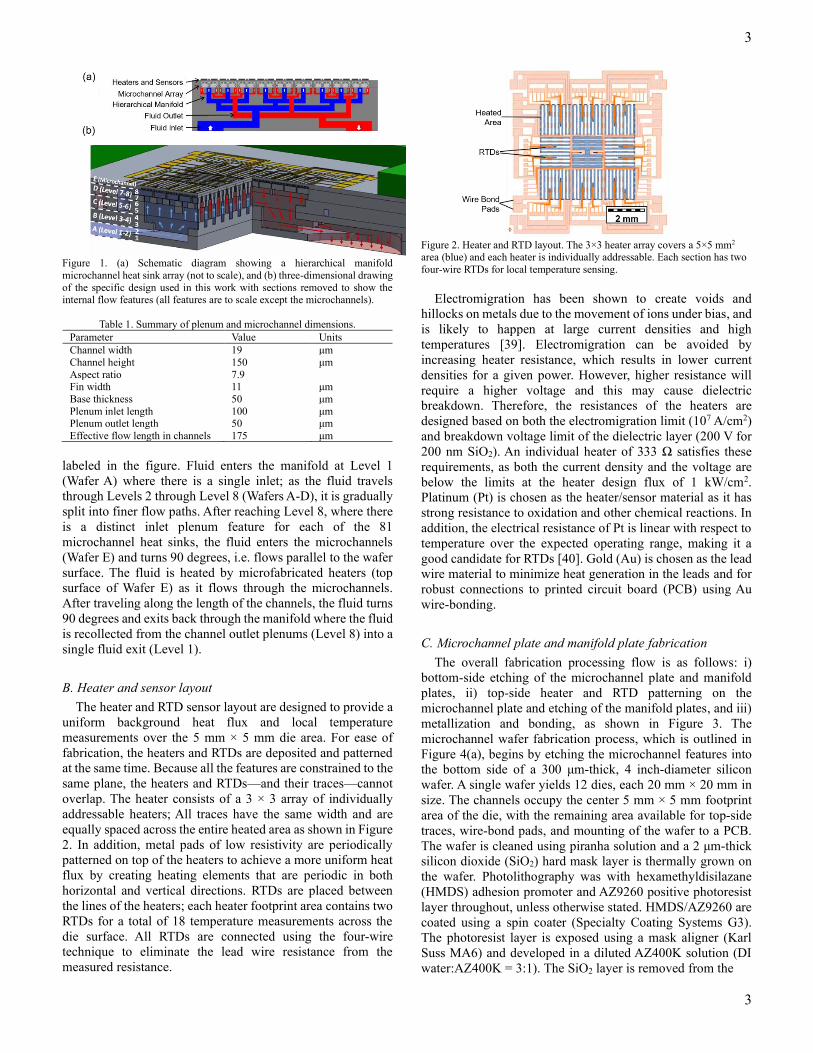
Figure 1. (a) Schematic diagram showing a hierarchical manifold
microchannel heat sink array (not to scale), and (b) three-dimensional drawing
of the specific design used in this work with sections removed to show the internal flow features (all features are to scale except the microchannels).
Table 1. Summary of plenum and microchannel dimensions.
Parameter Value Units
Channel width 19 μm
Channel height 150 μm
Aspect ratio 7.9 Fin width 11 μm
Base thickness 50 μm
Plenum inlet length 100 μm Plenum outlet length 50 μm
Effective flow length in channels 175 μm
labeled in the figure. Fluid enters the manifold at Level 1
(Wafer A) where there is a single inlet; as the fluid travels
through Levels 2 through Level 8 (Wafers A-D), it is gradually
split into finer flow paths. After reaching Level 8, where there
is a distinct inlet plenum feature for each of the 81
microchannel heat sinks, the fluid enters the microchannels
(Wafer E) and turns 90 degrees, i.e. flows parallel to the wafer
surface. The fluid is heated by microfabricated heaters (top
surface of Wafer E) as it flows through the microchannels.
After traveling along the length of the channels, the fluid turns
90 degrees and exits back through the manifold where the fluid
is recollected from the channel outlet plenums (Level 8) into a
single fluid exit (Level 1).
B. Heater and sensor layout
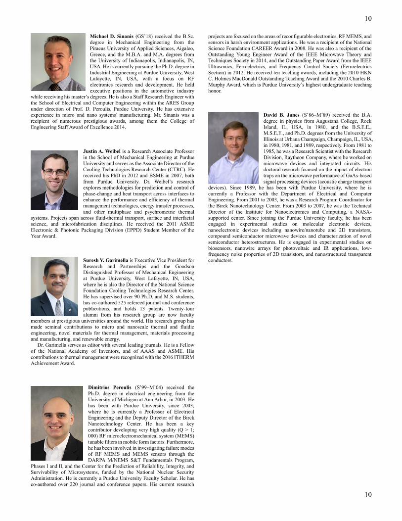
The heater and RTD sensor layout are designed to provide a
uniform background heat flux and local temperature
measurements over the 5 mm × 5 mm die area. For ease of
fabrication, the heaters and RTDs are deposited and patterned
at the same time. Because all the features are constrained to the
same plane, the heaters and RTDs—and their traces—cannot
overlap. The heater consists of a 3 × 3 array of individually
addressable heaters; All traces have the same width and are
equally spaced across the entire heated area as shown in Figure
2. In addition, metal pads of low resistivity are periodically
patterned on top of the heaters to achieve a more uniform heat
flux by creating heating elements that are periodic in both
horizontal and vertical directions. RTDs are placed between
the lines of the heaters; each heater footprint area contains two
RTDs for a total of 18 temperature measurements across the
die surface. All RTDs are connected using the four-wire
technique to eliminate the lead wire resistance from the
measured resistance.
Figure 2. Heater and RTD layout. The 3×3 heater array covers a 5×5 mm2 area (blue) and each heater is individually addressable. Each section has two
four-wire RTDs for local temperature sensing.
Electromigration has been shown to create voids and
hillocks on metals due to the movement of ions under bias, and
is likely to happen at large current densities and high
temperatures [39]. Electromigration can be avoided by
increasing heater resistance, which results in lower current
densities for a given power. However, higher resistance will
require a higher voltage and this may cause dielectric
breakdown. Therefore, the resistances of the heaters are
designed based on both the electromigration limit (107 A/cm2)
and breakdown voltage limit of the dielectric layer (200 V for
200 nm SiO2). An individual heater of 333 Ω satisfies these
requirements, as both the current density and the voltage are
below the limits at the heater design flux of 1 kW/cm2.
Platinum (Pt) is chosen as the heater/sensor material as it has
strong resistance to oxidation and other chemical reactions. In
addition, the electrical resistance of Pt is linear with respect to
temperature over the expected operating range, making it a
good candidate for RTDs [40]. Gold (Au) is chosen as the lead
wire material to minimize heat generation in the leads and for
robust connections to printed circuit board (PCB) using Au
wire-bonding.
C. Microchannel plate and manifold plate fabrication
The overall fabrication processing flow is as follows: i)
bottom-side etching of the microchannel plate and manifold
plates, ii) top-side heater and RTD patterning on the
microchannel plate and etching of the manifold plates, and iii)
metallization and bonding, as shown in Figure 3. The
microchannel wafer fabrication process, which is outlined in
Figure 4(a), begins by etching the microchannel features into
the bottom side of a 300 μm-thick, 4 inch-diameter silicon
wafer. A single wafer yields 12 dies, each 20 mm × 20 mm in
size. The channels occupy the center 5 mm × 5 mm footprint
area of the die, with the remaining area available for top-side
traces, wire-bond pads, and mounting of the wafer to a PCB.
The wafer is cleaned using piranha solution and a 2 μm-thick
silicon dioxide (SiO2) hard mask layer is thermally grown on
the wafer. Photolithography was with hexamethyldisilazane
(HMDS) adhesion promoter and AZ9260 positive photoresist
layer throughout, unless otherwise stated. HMDS/AZ9260 are
coated using a spin coater (Specialty Coating Systems G3).
The photoresist layer is exposed using a mask aligner (Karl
Suss MA6) and developed in a diluted AZ400K solution (DI
water:AZ400K = 3:1). The SiO2 layer is removed from the

4
4
Figure 3. Overall fabrication flow: i) bottom manifold and microchannel etch,
ii) top manifold and microchannel etch and heater/RTD patterning, iii)
interface metallization, assembly and bonding of all chips (not to scale, refer to Figure 1(b) for wafer labels A-E and level numbers 1-8).
open areas using a plasma dry etch (Surface Technology
Systems-Advanced Oxide Etch). The microchannels are then
etched to the desired depth using the Bosch process (STS-
Advanced Silicon Etch). For the etching of high-aspect-ratio
microchannels, the photoresist provides the soft mask after
microchannel patterning while the SiO2 provides sharper edges
and more vertical sidewalls. The key DRIE parameters are
listed in Table 2. Once the channels are etched, the photoresist
and SiO2 layers are removed using PRS2000 and buffered
oxide etch (BOE), respectively.
Heater and RTD patterns are fabricated directly on the top
side of the microchannel wafer. After the microchannel etch
process, a 200 nm-thick layer of SiO2 is thermally grown on
the wafer as a dielectric barrier. The same photolithography
procedures as for the microchannel patterning are employed,
and backside alignment was used to align the heater and RTD
patterns with respect to the microchannels. Once the patterns
are defined, 5 nm of Titanium (Ti) and then 20 nm of Pt are
deposited via electron beam evaporation (CHA Industries,
Inc.). This was done at a pressure level of 2.0 × 10⁻⁶ torr and
the deposition rate was 1.0 Å/s. A lift-off process is performed
by stripping off the photoresist using PRS2000. To fabricate
the heater and RTD lead wires, this lithography procedure is
repeated with two differences: the trace locations are defined
using a new mask and the metal depositions are 10 nm of Ti
and then 400 nm of Au.
Because the hierarchical manifold requires a large number
of layers for flow distribution, etching features into both sides
reduces the required number of wafers and bonding interfaces,
while also mitigating risk for misalignment between layers.
Two Levels are fabricated in each wafer, by etching from the
bottom side and then from the top side, with the patterns from
the two Levels meeting at the middle of the wafer. The
processing steps in manifold wafer fabrication are shown in
Figure 4(b). The 500 μm-thick wafers are cleaned and oxidized
with a 2 μm-thick SiO2 layer. The fabrication procedure
follows that used for the microchannel etch and the same
procedure is repeated on the opposite side of the wafer.
Backside lithography is used to align with the features already
etched in the wafer.
Figure 5(a) shows a microscope image of the heaters and
RTDs deposited on the opposite side of microchannel wafer
Figure 4. Cross-section of the fabrication process. a) microchannel and heater/RTD bottom side: (i) HMDS and photoresist (PR) coating; (ii)
microchannel lithography; (iii) SiO2 and Si etch; Top side: (iv) PR removal,
BOE & re-oxidation; (v) heater/RTD backside lithography; (vi) Ti and Pt deposition; (vii) lift-off; (viii) lead wires lithography; (ix) Ti and Au deposition;
(x) lift-off. b) manifold bottom: (i) PR coating and bottom side lithography;
(ii) SiO2 & Si etch. Top side: (iii) PR removal, BOE & re-oxidation; (iv) PR coating and top side lithography; (v) SiO2 & Si etch; (vi) PR removal and BOE.
Table 2. Key parameters using for deep reactive ion etching (DRIE) of the high-aspect-ratio microchannels.
Parameter Value Units
Etch rate (approx.) 3 μm/min
Etch step time 10 s
Passivation step time 10 s
RF power 1000 W
Platen power 10 W C4F8 flow rate 100 SCCM
SF6 flow rate 250 SCCM
O2 flow rate 30 SCCM
(Level E). Heating elements are clearly patterned in the 5 × 5
mm2 area, and RTDs are located in between the heaters. Each
heater is connected to Au traces for wirebonding. Figure 5(b)
shows a scanning electron microscope (SEM) image of the
cross section of the etched microchannels. Straight walls are
achieved and all channels have consistent width; the side walls
and bottom surfaces are smoothly finished.
D. Assembly and Integration
All layers of the manifold and microchannels are joined to
seal surfaces between the fluid routing features and prevent
fluid from bypassing the microchannels. An evaluation of
thermocompression bonding was performed using two dummy
silicon wafers, one containing through plenum features and
another with etched microchannels (nominally 15 μm × 150
μm). The samples were thermocompression bonded, diced,
and the open plenum features sealed to evaluate the leakage
rate of helium. The leakage rate was measured to be <1.3×10-
7 atm-cc/sec across 4 samples. The bonds were also subjected
to 500 temperature cycles (MIL-STD-883, Condition B, -55 to
+125°C) without failure. Based on these hermiticity results and

5
5
Figure 5. (a) Microscope image of fabricated heater/RTD layer. Heating
elements (Pt) are located in a 5 × 5 mm2 area and 18 RTDs are placed in between the heaters. (b) SEM image of the microchannel cross-section. The
width and depth of each channel is 19 μm and 150 μm, respectively.
visual inspection, thermocompression bonding was selected as
the sealing method for the test samples used in this work.
Prior to bonding, the microchannel and manifold wafers are
cleaned using piranha solution. After cleaning, 50 nm of Ti and
500 nm of Au are deposited on both sides of the manifold
wafers using a magnetron sputtering system (MANTIS
Deposition CUSP-Series); the Ti layer is used to increase
adhesion of the subsequent Au layer. The sputtering system
pressure during deposition is held at 7.3 ×10⁻³ Torr and the DC
deposition current is 0.1 A. The sample is rotated during
deposition to improve uniformity across the wafer. The
microchannel wafer is coated using the same deposition
process on the channel side. The wafers are then diced into 20
mm × 20 mm dies for bonding (Disco DAD-2H/6 Dicing Saw).
Figure 6(a-e) shows the metallized and diced dies.
A custom-made, Macor ceramic assembly fixture is used to
align the microchannel die and manifold dies during
thermocompression bonding. The assembly and alignment is
completed in a cleanroom to prevent any contamination at the
interfaces. Once the manifold and microchannel dies are
stacked in order, as shown in Figure 6(a-e), the fixture is
installed in the vacuum chamber of a bonding facility. Bonding
is performed by heating the assembly stack to 350 °C while
compressing at a pressure of 500 kPa for 1 h. The assembled
fluid features, including the hierarchical manifold (dies from
Wafers B-E), are confined to a 5 mm × 5 mm × 2.3 mm
working envelope. After thermocompression bonding, the die
assembly is attached to the underside of a custom-designed
PCB using adhesive tape. The heaters and RTDs are then
electrically connected to the PCB bond pads using gold wire
bonds as shown in Figure 6(f). Each of the background heaters
and RTDs are wirebonded (West Bond 7400A Ultrasonic
Wedge Bonder) separately such that they can be addressed and
monitored individually. A dummy chip is prepared to confirm
the reliability of the custom heaters and RTDs at the maximum
Figure 6. (a-d) Top view of the metallized manifold dies and (e) microchannel die after stacking. (f) Photograph of the fully assembled hierarchical manifold
microchannel heat sink array test vehicle, with inset showing the wirebonded
chip.
operating temperature. A constant current density (4.8×10⁶
A/cm2) was applied to the base heater and the chip temperature
was monitored by the central RTD. The temperature recorded
by the RTD was initially at 155 °C but decreased rapidly within
the first few hours as the heater resistance decreased. Because
the heater resistance would be expected to increase if degraded
by electromigration, this reduction in the heater resistance is
attributed to an annealing effect caused by Joule heating.
Afterward, the temperature remains stable at 138 ± 2 °C and
the resistance of heater slowly increases by 1% over a period
of 378 h, which causes a slight temperature increase due to the
increased heating power at constant current density; no failure
was observed. To calibrate the heater resistance before testing,
heaters are annealed at 180 °C in a laboratory oven for 24 h.
To characterize the manifold feature alignment, one sample
was diced normal to the flow direction in the microchannels,
polished, and imaged using a microscope, as shown in Figure
7. The arrows indicate the inlet fluid path through the
manifolds. The results reveal that there are no gaps between
the plates and that the flow features are aligned within a few
microns.
III. EXPERIMENTAL METHODS
A. Electrical measurement and calibration details
A wiring diagram of the electrical components used to
measure the voltage and current to each of the heaters, and to
adjust the power to each of the heaters, is shown in Figure 8. A
single DC power supply (Sorensen XG100-8.5) is used to
power all of the heaters. While the design of each individual
heater element on the test chip is identical, slight differences
in metal deposition thickness, trace length, wire bond
resistance, lead wire length, and operational temperature can
2 mm
(a)
(b)

6
6
Figure 7. Cross-section image of the bonded manifold and microchannel test
chip assembly with a magnified inset image of the top plenum and
microchannel features (refer to Figure 1(b) for wafer labels A-E and level numbers 1-8).
lead to small differences in their resistance. To ensure uniform
heat flux across the chip surface throughout testing, a
potentiometer (Ohmite RES25RE) is added in series with each
of the heaters; this provides a variable resistance that is used to
adjust the voltage drop of each parallel branch and thus
equalize the power applied by each heater. A voltage divider
circuit (TE Connectivity 1622796-6, 10 kΩ ± 0.1%; TE
Connectivity 8-1879026-9, 499 kΩ ± 0.1%) is wired in parallel
to each heater of the test chip, which is used to step down the
voltage below the 10 V limit of the data acquisition hardware
(National Instruments cDAQ-9178). For instance, as shown in
the Figure 8, the voltage across 𝑅1 (𝑉1) is calculated using
𝑉1 = 𝑉𝑚𝑒𝑎𝑠,1 ∗ ((𝑅𝑑𝑖𝑣1 + 𝑅𝑑𝑖𝑣2) 𝑅𝑑𝑖𝑣2⁄ ) , where 𝑉𝑚𝑒𝑎𝑠,1 is
acquired from the data acquisition hardware and 𝑅𝑑𝑖𝑣1 and
𝑅𝑑𝑖𝑣2 are known. The voltage drop (𝑉𝑠ℎ𝑢𝑛𝑡) across a shunt
resistor (𝑅𝑠ℎ𝑢𝑛𝑡) (Vishay Y14880R10000B9R, 0.1 Ω ± 0.1%)
wired in series to each heater is used to calculate the current
through each heater: 𝐼𝑁 = (𝑉𝑠ℎ𝑢𝑛𝑡,𝑁 𝑅𝑠ℎ𝑢𝑛𝑡⁄ ) . The total
voltage drop and current are measured using the same
techniques and are used to verify the individual measurements.
To calibrate the on-chip RTDs, the test chip is placed in a
laboratory oven along with a Pt100 RTD (PR-10-3-100,
Omega) that is used as the known reference temperature. The
electrical resistance of the on-chip RTDs was measured at two
different temperature levels: 50 °C and 100 °C. A linear fit is
used to determine the relationship between electrical resistance
and temperature for each of the 18 RTDs across the chip
surface.
B. Thermal and hydrodynamic testing procedure
Prior to testing, the working fluid HFE-7100 is degassed via
vigorous boiling and subsequent capture of the vapor;
noncondensable gases escape during this process, leaving pure
working fluid to be used for testing. HFE-7100 was chosen
because of its high dielectric strength and low attenuation of
RF signals; its boiling point is 61 °C at 100 kPa . A two-phase
flow loop is used to deliver fluid to the test section at a constant
and known flow rate, inlet temperature, and outlet pressure.
The magnetically-coupled gear pump (GB-P23, Micropump)
provides a constant flow rate that is independent of the system
Figure 8. Electrical wiring diagram showing the components used to measure
heater power to the test vehicle. The voltage divider circuits (blue) consist of
two resistors (Rdiv1 = 499 kΩ, Rdiv2 = 10 kΩ) and each shunt resistor (red, Rshunt = 0.1 Ω, Rshunt,tot = 0.2 Ω) is used for current measurement. The potentiometers
(green, Rpot = 0-25 Ω) are added to adjust and equalize power to each heater.
pressure drop; the flow rate is measured using a Coriolis mass
flow meter (CMF010M, Micromotion). The differential
pressure drops across the entire chip and across the
microchannels are measured (PX2300, Omega) using pressure
taps located in the inlet/outlet of manifold and microchannels,
respectively. A detailed description of this flow loop is
available in Ref. [41]. To characterize the two-phase heat sink
performance under boiling conditions, the fluid temperature at
the inlet to the test section was set to achieve a constant,
relatively small subcooling below the saturation temperature.
Experimental testing was performed at a fixed inlet
temperature of 59 °C (~6 °C below the saturation temperature
at the outlet pressure), fixed absolute outlet pressure of 121 kPa,
and fluid flow rates ranging from 150 to 350 g/min. During
testing, the heat input to the test chip heaters begins at 0 W and
is incremented in steps until a maximum chip temperature of
120 °C is reached, with the steady-state data (temperatures,
pressures, voltages, currents, and flow rate) being recorded at
each heat input level. The fluid pressure drop is measured
between the inlet and outlet streams at Level 1 and Level 8
(Figure 1(b)); the measurement at Level 1 provides the total
pressure drop while the measurement at Level 8 provides the
channel pressure drop.
C. Data reduction
Electrical power supplied to each heater is calculated using
P = V×I, where V is electrical voltage and I is electrical current.
The total power supplied to the heaters, Ptotal, is then ca
lculated by summing the power to each of the heaters.
Most of the applied heat is absorbed into the fluid via
convective and boiling heat transfer; however, some of the heat
is conducted into the test fixture and lost to the ambient. This
heat loss was estimated prior to testing using the method
outlined in Ref. [38] and was found to be 𝑄𝑙𝑜𝑠𝑠 = 0.02768 ∗
(𝑇𝑐ℎ𝑖𝑝,𝑎𝑣𝑔 − 𝑇𝑎𝑚𝑏) . The net heat input is calculated by
subtracting the calibrated heat loss, Qloss, from the supplied

7
7
Figure 9. Average chip temperature as a function of base heat flux at flow rates of 150, 230, 290, and 350 g/min.
electrical power as Qin = Ptotal − Qloss. The base heat flux is
calculated by dividing the net heat input by the base footprint
area, Ab. Pressure drop is measured at the inlet and outlet to the
manifold as well as the inlet and outlet to the channels.
IV. RESULTS
A. Thermal performance
Figure 9 shows the average chip temperature as a function
of base heat flux at four different fluid flow rates. Fluid enters
the test chip at 59 °C and is heated as it flows along the length
of the channels. At low heat fluxes (< 100 W/cm2 approx.), the
surface temperature rise is not sufficient to initiate boiling of
the liquid. In this single-phase region, convective heat transfer
results in a linear chip temperature increase with heat flux at
each flow rate. At higher heat fluxes, the fluid transitions to
boiling, resulting in a lower temperature rise for a given
increase in heat flux in the two-phase region compared to the
single-phase regime; the slope of the curves in the two-phase
regime is insensitive to flow rate, indicating that the boiling
process governs heat transfer to the fluid. At some critical heat
flux, the surface temperature experiences a sudden increase
past the 120 °C limit and the heater power is cutoff; the last
steady-state data point before this threshold terminates each
curve in Figure 9. There is a slight degradation in performance
(increasing slope) in each curve as the critical heat flux is
approached. The critical heat flux is highly dependent on the
fluid flow rates and as flow rate increases, higher heat fluxes
can be dissipated before critical heat flux is encountered. The
highest heat flux dissipated at a flow rate of 150 g/min is 305
W/cm² and at 350 g/min is 660 W/cm², an increase of 116%. A
more thorough analysis of performance trends in MMC heat
sinks during two-phase operation is available in [38], [41].
B. Pressure drop
Figure 10(a) shows the measured total pressure drop across
the entire test chip, which includes pressure drop in the inlet
and outlet manifold as well as the microchannels. For each
flow rate, the pressure drop is relatively constant in the single-
phase region. Upon boiling incipience, the bulk fluid density
decreases causing an increase in fluid velocity and hence
Figure 10. (a) Total pressure drop as a function of base heat flux at flow rates
of 150, 230, 290, and 350 g/min and (b) comparison of the total pressure drop
(open symbols) versus microchannel pressure drop (closed symbols) at a flow rate of 350 g/min.
pressure drop. The two-phase pressure drop increases with heat
flux due to the increase in vapor generation with increasing
heat flux at a given flow rate. The pressure drop increases with
increasing flow rate in both the single- and two-phase regions,
as expected. Figure 10(b) plots both the total pressure drop
across the test chip and the pressure drop across the
microchannels for the highest flow rate of 350 g/min. A
majority of the total pressure drop occurs in the manifold flow
features; the channel pressure drop accounts for only 20% to
27% of the total pressure drop, depending on the heat flux. This
is important to note because thermal performance is governed
by the channel size; due to the discretization of the heat sink
into a 9 × 9 array with very short flow paths, the pressure drop
across the channels can be maintained at only 27 kPa for the
maximum heat flux dissipation of 660 W/cm². In the current
design, the large maximum total pressure drop of 138 kPa is
caused by the restriction of the manifold flow features to a
compact envelope of only 5 mm × 5 mm × 2.3 mm such that
the observed volumetric heat dissipation of 2870 W/cm3 can
be achieved.
C. Discussion
To illustrate the compactness of the 9 × 9 heat sink array, its
Flow Rate
(b)
(a)

8
8
Figure 11. (a) Average chip temperature and (b) pressure drop for the 3 × 3
array and the 9 × 9 array. A similar nominal microchannel size of
approximately 15 μm × 150 μm was used in both array designs. (Channel pressure drop for 3 × 3 array test vehicle was not available.)
thermal and hydraulic performance are compared with our
previous work. Figure 11(a) shows the 350 g/min data from the
current test vehicle having a 9 × 9 heat sink array compared to
data from Drummond et al. [41] for a 3 × 3 array at a similar
flow rate of 360 g/min. The samples have similar nominal
channel geometries of approximately 15 μm × 150 μm.
Overall, the thermal performance is very similar for the two
different test vehicles. While the flow length and number of
parallel flow paths differ significantly, thermal performance is
known to be largely governed by channel size and fluid quality
during two-phase operation in confined microchannels, which
are essentially the same across these data sets. Even though the
thermal performance is very similar between the designs on a
heat flux basis, the primary advantage of the 9 × 9 heat sink
array is the small volumetric envelope of the compact
integrated manifold, which is significantly reduced compared
to the 3 × 3 array manifold. All functional flow features could
be confined into a 5 × 5 × 2.3 mm3 for the 9 × 9 manifold in
the current work compared to an envelope of 25 × 8 × 10 mm3
for the 3 × 3 manifold in our prior work. This translates to a
maximum volumetric heat dissipation of 2870 W/cm³ for the 9
× 9 array compared to a maximum of only 285 W/cm³ for the
3 × 3 array. However, this compact manifold design requires
smaller manifold flow features that increase the total pressure
drop; Figure 11(b) shows the total pressure drop for the 9 × 9
array compared to that the 3 × 3 array. The channel pressure
drop for the 9 × 9 array is also shown for reference. Even
though the 3 × 3 array would be expected to have a higher
channel pressure drop (it was not measured), the 9 × 9 array
still has a notably higher total pressure drop at a given heat
flux, due to the dominant contribution of the manifold flow
resistance to the overall pressure drop.
V. CONCLUSION
A compact hierarchical manifold microchannel heat sink
was fabricated and tested. The hierarchical manifold consists
of 8 fluid routing levels which distribute fluid uniformly to a
dense 9 × 9 array of embedded microchannel heat sinks. All
fluid features are fabricated using photolithography and DRIE
processes. The individually addressable heaters and 4-wire
RTDs are patterned directly on top of the microchannel wafer
to provide heating and local temperature sensing. The
fabricated dies are aligned using a custom-designed assembly
fixture and thermocompression bonded. With stringent size
constraints on most heat sinks, this compact, robust manifold
design provides a functional manifold within a total envelope
volume of 5 × 5 × 2.3 mm3.
The thermal performance of the 9 × 9 array heat sink at a
given flow rate is very similar to previous work that
investigated 3 × 3 arrays. However, due to the integration of a
compact manifold, a volumetric heat density of up to 2870
W/cm3 is dissipated from the 9 × 9 array, an order of magnitude
higher than that with the 3 × 3 array. While the microchannel
pressure drop was only 27 kPa for the maximum heat flux
dissipation of 660 W/cm2, a majority of the pressure drop (80%
of the total) occurs in the manifold for these extremely small
fluid flow features, resulting in a total pressure drop of 138 kPa
at this heat flux.
ACKNOWLEDGMENT
Special thanks to David H. Altman at Raytheon Integrated
Defense Systems for performing the hermicity and
temperature cycling tests.
REFERENCES
[1] A. Bar-Cohen, J. J. Maurer, and J. G. Felbinger, “DARPA’s
Intra/Interchip Enhanced Cooling (ICECool) Program,” in CS MANTECH Conference, New Orleans, LA, May, 2013, pp. 171–174.
[2] J. Jiménez, “Laser diode reliability: Crystal defects and degradation
modes,” C. R. Physique., vol. 4, no. 6, pp. 663–673, 2003. [3] M. A. Green, “General temperature dependence of solar cell
performance and implications for device modelling,” Prog. Photovolt.
Res. Appl., vol. 11, no. 5, pp. 333–340, 2003. [4] P. Singh and N. M. Ravindra, “Solar energy materials & solar cells
temperature dependence of solar cell performance — an analysis,” Sol.
Energy Mater. Sol. Cells, vol. 101, pp. 36–45, 2012. [5] T. J. Chainer, M. D. Schultz, P. R. Parida, and M. A. Gaynes, “Improving
data center energy efficiency with advanced thermal management,”
IEEE Trans. Components, Packag. Manuf. Technol., vol. 7, no. 8, pp. 1228–1239, Aug. 2017.
[6] R. Abebe et al., “Integrated motor drives: state of the art and future
trends,” IET Electr. Power Appl., vol. 10, no. 8, pp. 757–771, Sep. 2016. [7] D. B. Tuckerman and R. F. W. Pease, “High-performance heat sinking
for VLSI,” IEEE Electron Device Lett, Vol. EDL-2, no. 5, pp. 126–129,
May, 1981. [8] G. L. Morini, “Single-phase convective heat transfer in microchannels:
A review of experimental results,” Int. J. Therm. Sci., vol. 43, no. 7, pp.
9 x 9 Array
3 x 3 Array
(b)
(a)

9
9
631–651, Jul, 2004. [9] C. B. Sobhan and S. V. Garimella, “A comparative analysis of studies on
heat transfer and fluid flow in microchannels,” Microscale Thermophys.
Eng., vol. 5, no. 4, pp. 293–311, Oct. 2001. [10] G. M. Harpole and J. E. Eninger, “Micro-channel heat exchanger
optimization,” in Proc. IEEE 7th semiconductor thermal measurement
and management symposium, Phoenix, AZ, 1991, pp. 59–63. [11] D. Copeland, M. Behnia, and W. Nakayama, “Manifold microchannel
heat sinks: isothermal analysis,” IEEE Trans. Components, Packag.
Manuf. Technol. Part A, vol. 20, no. 2, pp. 96–102, Jun. 1997. [12] J. H. Ryu, D. H. Choi, and S. J. Kim, “Three-dimensional numerical
optimization of a manifold microchannel heat sink,” Int. J. Heat Mass
Transf., vol. 46, no. 9, pp. 1553–1562, Apr. 2003. [13] W. Escher, B. Michel, and D. Poulikakos, “A novel high performance,
ultra thin heat sink for electronics,” Int. J. Heat Fluid Flow, vol. 31, no.
4, pp. 586–598, Aug. 2010. [14] L. Boteler, N. Jankowski, P. McCluskey, and B. Morgan, “Numerical
investigation and sensitivity analysis of manifold microchannel coolers,”
Int. J. Heat Mass Transf., vol. 55, no. 25–26, pp. 7698–7708, Dec. 2012. [15] T. Baummer, E. Cetegen, M. Ohadi, and S. Dessiatoun, “Force-fed
evaporation and condensation utilizing advanced micro-structured
surfaces and micro-channels,” Microelectronics J., vol. 39, no. 7, pp.
975–980, Jul. 2008.
[16] C. S. Sharma, M. K. Tiwari, B. Michel, and D. Poulikakos,
“Thermofluidics and energetics of a manifold microchannel heat sink for electronics with recovered hot water as working fluid,” Int. J. Heat Mass
Transf., vol. 58, no. 1–2, pp. 135–151, Mar. 2013. [17] S. Sarangi, K. K. Bodla, S. V. Garimella, and J. Y. Murthy, “Manifold
microchannel heat sink design using optimization under uncertainty,” Int.
J. Heat Mass Transf., vol. 69, pp. 92–105, Feb. 2014. [18] M. A. Arie, A. H. Shooshtari, S. V. Dessiatoun, E. Al-Hajri, and M. M.
Ohadi, “Numerical modeling and thermal optimization of a single-phase
flow manifold-microchannel plate heat exchanger,” Int. J. Heat Mass Transf., vol. 81, pp. 478–489, Feb. 2015.
[19] Y. Zhang, S. Wang, and P. Ding, “Effects of channel shape on the cooling
performance of hybrid micro-channel and slot-jet module,” Int. J. Heat Mass Transf., vol. 113, pp. 295–309, Oct. 2017.
[20] W. Tang, L. Sun, H. Liu, G. Xie, Z. Mo, and J. Tang, “Improvement of
flow distribution and heat transfer performance of a self-similarity heat sink with a modification to its structure,” Appl. Therm. Eng., vol. 121,
pp. 163–171, Jul. 2017.
[21] R. S. Andhare, A. Shooshtari, S. V. Dessiatoun, and M. M. Ohadi, “Heat transfer and pressure drop characteristics of a flat plate manifold
microchannel heat exchanger in counter flow configuration,” Appl.
Therm. Eng., vol. 96, pp. 178–189, Mar. 2016. [22] L. Tadrist, “Review on two-phase flow instabilities in narrow spaces,”
Int. J. Heat Fluid Flow, vol. 28, no. 1, pp. 54–62, Feb. 2007.
[23] T. Van Oevelen, J. A. Weibel, and S. V. Garimella, “Predicting two-phase flow distribution and stability in systems with many parallel heated
channels,” Int. J. Heat Mass Transf., vol. 107, pp. 557–571, Apr. 2017.
[24] T. Van Oevelen, J. A. Weibel, and S. V. Garimella, “The effect of lateral thermal coupling between parallel microchannels on two-phase flow
distribution,” Int. J. Heat Mass Transf., vol. 124, pp. 769–781, Sep. 2018.
[25] T. Brunschwiler et al., “Direct liquid jet-impingement cooling with micronsized nozzle array and distributed return architecture,” in Proc. of
the Intersociety Conference on Thermomechanical Phenomena in
Electronic Systems (ITHERM), San Diego, CA, 2006, pp. 196–203. [26] J. P. Calame, D. Park, R. Bass, R. E. Myers, and P. N. Safier,
“Investigation of hierarchically branched-microchannel coolers
fabricated by deep reactive ion etching for electronics cooling applications,” J. Heat Transfer, vol. 131, no. 5, pp. 051401, May. 2009.
[27] B. Dang et al., “Integration and Packaging of Embedded Radial Micro-
Channels for 3D Chip Cooling,” in IEEE 66th Electronic Components and Technology Conference (ECTC), Las Vegas, NV, 2016, pp. 1271–
1277.
[28] M. D. Schultz et al., “Microfluidic two-phase cooling of a high power microprocessor part A: Design and fabrication,” in IEEE 16th Intersociety
Conference on Thermal and Thermomechanical Phenomena in
Electronic Systems (ITHERM), Orlando, FL, 2017, pp. 450–457. [29] E. G. Colgan et al., “A practical implementation of silicon microchannel
coolers for high power chips,” IEEE Trans. Components Packag.
Technol., vol. 30, no. 2, pp. 218–225, 2007. [30] W. Escher, T. Brunschwiler, B. Michel, and D. Poulikakos,
“Experimental Investigation of an Ultrathin Manifold Microchannel
Heat Sink for Liquid-Cooled Chips,” J. Heat Transfer, vol. 132, no. 8,
pp. 081402, 2010. [31] J.-Y. Chang et al., “Convective performance of package based single
phase microchannel heat exchanger,” in Proc. of ASME Summer Heat
Transfer Conference, HT, San Francisco, CA, Jul. 2005, vol. 2, pp. 889–894.
[32] K. Petersen, P. Barth, J. Poydock, J. Brown, J. Mallon, and J. Bryzek,
“Silicon fusion bonding for pressure sensors,” in IEEE Technical Digest on Solid-State Sensor and Actuator Workshop, Hilton Head Island, SC,
1988, pp. 144–147.
[33] Y. C. Chan, Y.-K. Lee, and Y. Zohar, “High-throughput design and fabrication of an integrated microsystem with high aspect-ratio sub-
micron pillar arrays for free-solution micro capillary electrophoresis,” J.
Micromech. Microeng., vol. 16, no. 4, pp. 699–707, Apr. 2006. [34] Y. T. Cheng, L. Lin, and K. Najafi, “Localized silicon fusion and eutectic
bonding for MEMS fabrication and packaging,” J. Microelectromech.
Syst., vol. 9, no. 1, pp. 3–8, Mar. 2000. [35] C. H. Tsau, S. M. Spearing, M. A. Schmidt, and S. Member, “Fabrication
of wafer-level thermocompression bonds,” J. Microelectromech. Syst.,
vol. 11, no. 6, pp. 641–647, 2002. [36] V. Sahu, Y. K. Joshi, A. G. Fedorov, J. Bahk, X. Wang, and A. Shakouri,
“Experimental characterization of hybrid solid-state and fluidic cooling
for thermal management of localized hotspots,” IEEE Trans.
Components, Packag. Manuf. Technol., vol. 5, no. 1, pp. 57–64, 2015.
[37] S. R. Rao, F. Houshmand, and Y. Peles, “Transient flow boiling heat-
transfer measurements in microdomains,” Int. J. Heat Mass Transf., vol. 76, pp. 317–329, 2014.
[38] K. P. Drummond et al., “Characterization of hierarchical manifold microchannel heat sink arrays under simultaneous background and
hotspot heating conditions,” Int. J. Heat Mass Transf., vol. 126, pp.
1289–1301, Nov. 2018. [39] P. S. Ho and T. Kwok, “Electromigration in metals,” Rep. Prog. Phys.,
vol. 52, p. 301, 1989.
[40] L. Crovini, A. Actis, G. Coggiola, and A. Mangano, “Accurate thermometry by means of industrial platinum resistance thermometers,”
Measurement, vol. 10, no. 1, pp. 31–38, Jan. 1992.
[41] K. P. Drummond et al., “A hierarchical manifold microchannel heat sink array for high-heat-flux two-phase cooling of electronics,” Int. J. Heat
Mass Transf., vol. 117, pp. 319–330, 2018.
Doosan Back received the B.S. degree in physics
from Sungkyunkwan University, Suwon, Korea and
the M.S. degree in electrical engineering from Columbia University in the City of New York, NY,
USA. He is currently pursuing the Ph.D. degree in
electrical and computer engineering at Purdue University, West Lafayette, IN, USA. His research
interests include silicon microelectronic devices and
nanostructures using nanowires and graphene. He is engaged in experimental studies on sensors, nanoarrays, and transparent
conductors.
Kevin P. Drummond received the B.S. and M.S. degree in mechanical engineering from Ohio
University, Athens, Ohio and the Ph.D. degree in
mechanical engineering from Purdue University, West Lafayette, IN, USA. He is currently a researcher at
IBM, Poughkeepsie, NY
10
10
Michael D. Sinanis (GS’18) received the B.Sc. degree in Mechanical Engineering from the
Piraeus University of Applied Sciences, Aigaleo,
Greece, and the M.B.A. and M.A. degrees from the University of Indianapolis, Indianapolis, IN,
USA. He is currently pursuing the Ph.D. degree in
Industrial Engineering at Purdue University, West Lafayette, IN, USA, with a focus on RF
electronics research and development. He held
executive positions in the automotive industry while receiving his master’s degrees. He is also a Staff Research Engineer with
the School of Electrical and Computer Engineering within the ARES Group
under direction of Prof. D. Peroulis, Purdue University. He has extensive experience in micro and nano systems’ manufacturing. Mr. Sinanis was a
recipient of numerous prestigious awards, among them the College of
Engineering Staff Award of Excellence 2014.
Justin A. Weibel is a Research Associate Professor
in the School of Mechanical Engineering at Purdue
University and serves as the Associate Director of the
Cooling Technologies Research Center (CTRC). He
received his PhD in 2012 and BSME in 2007, both
from Purdue University. Dr. Weibel’s research explores methodologies for prediction and control of
phase-change and heat transport across interfaces to enhance the performance and efficiency of thermal
management technologies, energy transfer processes,
and other multiphase and psychrometric thermal systems. Projects span across fluid-thermal transport, surface and interfacial
science, and microfabrication disciplines. He received the 2011 ASME
Electronic & Photonic Packaging Division (EPPD) Student Member of the Year Award.
Suresh V. Garimella is Executive Vice President for
Research and Partnerships and the Goodson Distinguished Professor of Mechanical Engineering
at Purdue University, West Lafayette, IN, USA,
where he is also the Director of the National Science Foundation Cooling Technologies Research Center.
He has supervised over 90 Ph.D. and M.S. students,
has co-authored 525 refereed journal and conference publications, and holds 13 patents. Twenty-four
alumni from his research group are now faculty
members at prestigious universities around the world. His research group has made seminal contributions to micro and nanoscale thermal and fluidic
engineering, novel materials for thermal management, materials processing
and manufacturing, and renewable energy. Dr. Garimella serves as editor with several leading journals. He is a Fellow
of the National Academy of Inventors, and of AAAS and ASME. His
contributions to thermal management were recognized with the 2016 ITHERM Achievement Award.
Dimitrios Peroulis (S’99–M’04) received the
Ph.D. degree in electrical engineering from the University of Michigan at Ann Arbor, in 2003. He
has been with Purdue University, since 2003,
where he is currently a Professor of Electrical Engineering and the Deputy Director of the Birck
Nanotechnology Center. He has been a key
contributor developing very high quality (Q > 1; 000) RF microelectromechanical system (MEMS)
tunable filters in mobile form factors. Furthermore,
he has been involved in investigating failure modes of RF MEMS and MEMS sensors through the
DARPA M/NEMS S&T Fundamentals Program,
Phases I and II, and the Center for the Prediction of Reliability, Integrity, and Survivability of Microsystems, funded by the National Nuclear Security
Administration. He is currently a Purdue University Faculty Scholar. He has
co-authored over 220 journal and conference papers. His current research
projects are focused on the areas of reconfigurable electronics, RF MEMS, and sensors in harsh environment applications. He was a recipient of the National
Science Foundation CAREER Award in 2008. He was also a recipient of the
Outstanding Young Engineer Award of the IEEE Microwave Theory and Techniques Society in 2014, and the Outstanding Paper Award from the IEEE
Ultrasonics, Ferroelectrics, and Frequency Control Society (Ferroelectrics
Section) in 2012. He received ten teaching awards, including the 2010 HKN C. Holmes MacDonald Outstanding Teaching Award and the 2010 Charles B.
Murphy Award, which is Purdue University’s highest undergraduate teaching
honor.
David B. Janes (S’86–M’89) received the B.A.
degree in physics from Augustana College, Rock
Island, IL, USA, in 1980, and the B.S.E.E., M.S.E.E., and Ph.D. degrees from the University of
Illinois at Urbana Champaign, Champaign, IL, USA,
in 1980, 1981, and 1989, respectively. From 1981 to 1985, he was a Research Scientist with the Research
Division, Raytheon Company, where he worked on
microwave devices and integrated circuits. His
doctoral research focused on the impact of electron
traps on the microwave performance of GaAs-based
signal processing devices (acoustic charge transport devices). Since 1989, he has been with Purdue University, where he is
currently a Professor with the Department of Electrical and Computer Engineering. From 2001 to 2003, he was a Research Program Coordinator for
the Birck Nanotechnology Center. From 2003 to 2007, he was the Technical
Director of the Institute for Nanoelectronics and Computing, a NASA-supported center. Since joining the Purdue University faculty, he has been
engaged in experimental studies on molecular electronic devices,
nanoelectronic devices including nanowire/nanotube and 2D transistors, compound semiconductor microwave devices and characterization of novel
semiconductor heterostructures. He is engaged in experimental studies on
biosensors, nanowire arrays for photovoltaic and IR applications, low-frequency noise properties of 2D transistors, and nanostructured transparent
conductors.