design automation for partially reconfigurable …...design automation for partially recon gurable...
TRANSCRIPT
NANYANG TECHNOLOGICAL UNIVERSITY
Design Automation for Partially
Reconfigurable Adaptive Systems
Vipin Kizheppatt
School of Computer Engineering
A thesis submitted to Nanyang Technological University
in partial fulfilment of the requirements for the degree of
Doctor of Philosophy
February 2015
THESIS ABSTRACT
Design Automation for Partially Reconfigurable
Adaptive Systems
by
Vipin KizheppattDoctor of Philosophy
School of Computer Engineering
Nanyang Technological University, Singapore
Adaptive systems have the ability to respond to environmental conditions, by mod-
ifying their processing at runtime. While this is easy to do in software systems,
modern algorithms can be computationally expensive, requiring powerful proces-
sors. At the same time hardware is not as flexible. Field programmable gate
arrays (FPGAs) are recognised as being suitable for adaptive systems implemen-
tation, due to their flexibility and high performance. New hybrid FPGA platforms
which integrate able processors with reconfigurable fabric provide a new platform
to further explore hardware reconfigurability. The use of partial reconfiguration
(PR) on FPGAs to implement adaptive systems has been proposed many times in
the literature. However the design process for partially reconfigurable systems is
complex and requires specialist knowledge on behalf of the application designer.
Hence, it has remained a rarely used capability outside of academic circles. We
propose a new approach to leverage PR within adaptive systems, by integrating
with, rather than circumventing, supported vendor tool flows, while automating
many of the steps that have made such designs more difficult in the past. This
makes it possible for system designers with less FPGA expertise to use PR when
designing adaptive systems.
Acknowledgements
First and foremost I would like to thank my mentor and supervisor Suhaib Fahmy
for selecting me as his first PhD student and giving an opportunity to work in this
vibrant university. His charm and enthusiasm have always helped me to perform
my research work under a relaxed and energetic environment. His guidance really
helped me to understand the research strategies under an academic environment.
I appreciate his ideas, suggestions, and especially the time he has taken to help
me correct mistakes and improve my writing.
I am really thankful to my friends and colleagues at the Centre for High Perfor-
mance Embedded Systems (CHiPES), especially Sharad Sinha, Shreejith Shanker,
Jiang Lianlian, Abhishek Jain, Ronak Bajaj, Thinh Pham, Abdullah Shamil, Hui
Yan Cheah, Dang Khoa Pham, Kavitha Jubin and Smitha Shreekumar for their
support and companionship. Chua Ngee Tat, laboratory executive at CHiPES,
was always ready to lend a helping hand whenever I faced software related issues.
I would also like to thank Associate Professor Vinod A Prasad (School of Com-
puter Engineering, NTU) and Professor Ian McLoughlin (University of Science
and Technology of China) for their encouragement and support during the courses
they taught me. I express my gratitude to other members of NTU ARCH research
group, Assoc. Prof. Douglas Leslie Maskell, Asst. Prof. Nachiket Kapre, Asst.
Prof. Arvind Easwaran and Asst. Prof. Kyle Rupnow for their guidance and
research support.
I am taking this opportunity to thank my previous employer Processor Systems
India Pvt. Ltd (Procsys), Bangalore, India for providing me an opportunity work
in a competitive industrial scenario. My interest in FPGAs was stimulated during
my employment and I would like to thank my former mentors Manjusha S and
Vinod N and my former manager Jaison T D for their guidance on FPGA based
systems design and industry standards, which were proven to be invaluable during
my research.
I like to thank my parents for their constant love and encouragement. I am in-
debted to the pain, and efforts they took to support me in pursuing higher studies.
Last but not the least, I would like to thank my wife for her constant support and
patience during my research work.
ii
Contents
Acknowledgements ii
List of Abbrevations x
1 Introduction 1
1.1 Adaptive Systems . . . . . . . . . . . . . . . . . . . . . . . . . . . . 3
1.2 FPGAs as an Adaptive Hardware Platform . . . . . . . . . . . . . . 4
1.3 Partial Reconfiguration . . . . . . . . . . . . . . . . . . . . . . . . . 6
1.4 Motivations . . . . . . . . . . . . . . . . . . . . . . . . . . . . . . . 8
1.5 Objectives . . . . . . . . . . . . . . . . . . . . . . . . . . . . . . . . 10
1.6 Contributions . . . . . . . . . . . . . . . . . . . . . . . . . . . . . . 10
1.7 Thesis Roadmap . . . . . . . . . . . . . . . . . . . . . . . . . . . . 11
1.8 Publications . . . . . . . . . . . . . . . . . . . . . . . . . . . . . . . 12
1.9 Open Source Releases . . . . . . . . . . . . . . . . . . . . . . . . . . 13
2 Background 15
2.1 Hardware Adaptive Systems Implementation . . . . . . . . . . . . . 16
2.2 Partial Reconfiguration . . . . . . . . . . . . . . . . . . . . . . . . . 18
2.3 PR Design Challenges . . . . . . . . . . . . . . . . . . . . . . . . . 19
2.4 Summary . . . . . . . . . . . . . . . . . . . . . . . . . . . . . . . . 21
3 Review of Literature 22
3.1 Architecture . . . . . . . . . . . . . . . . . . . . . . . . . . . . . . . 22
3.1.1 Academic and Non-Commercial Architectures . . . . . . . . 24
3.1.2 Commercial Devices Supporting PR . . . . . . . . . . . . . . 27
3.2 Design Methodologies . . . . . . . . . . . . . . . . . . . . . . . . . . 33
3.2.1 Vendor PR Design Flows . . . . . . . . . . . . . . . . . . . . 33
3.2.1.1 Xilinx PR Flow . . . . . . . . . . . . . . . . . . . . 33
3.2.1.2 Altera PR Flow . . . . . . . . . . . . . . . . . . . . 35
3.2.2 Academic PR Development Tools . . . . . . . . . . . . . . . 37
3.2.2.1 OpenPR Tool Flow . . . . . . . . . . . . . . . . . . 37
3.2.2.2 GoAhead Tool Flow . . . . . . . . . . . . . . . . . 38
3.2.2.3 Other PR Implementation Tools . . . . . . . . . . 39
3.3 Low-Level PR Control Techniques . . . . . . . . . . . . . . . . . . . 43
3.3.1 Runtime Placement . . . . . . . . . . . . . . . . . . . . . . . 43
iii
CONTENTS iv
3.3.2 Overhead Reduction . . . . . . . . . . . . . . . . . . . . . . 45
3.4 Applications of Partial Reconfiguration . . . . . . . . . . . . . . . . 46
3.4.1 Communication Systems . . . . . . . . . . . . . . . . . . . . 47
3.4.2 Multimedia . . . . . . . . . . . . . . . . . . . . . . . . . . . 47
3.4.3 Aerospace Applications . . . . . . . . . . . . . . . . . . . . . 48
3.4.4 Networking . . . . . . . . . . . . . . . . . . . . . . . . . . . 49
3.4.5 Automotive Systems . . . . . . . . . . . . . . . . . . . . . . 50
3.4.6 Computational Science . . . . . . . . . . . . . . . . . . . . . 50
3.4.7 Computing Systems . . . . . . . . . . . . . . . . . . . . . . . 51
3.4.8 Machine Learning . . . . . . . . . . . . . . . . . . . . . . . . 51
3.5 Summary . . . . . . . . . . . . . . . . . . . . . . . . . . . . . . . . 52
4 Partitioning for Partial Reconfiguration 53
4.1 Introduction . . . . . . . . . . . . . . . . . . . . . . . . . . . . . . . 53
4.2 Related Work . . . . . . . . . . . . . . . . . . . . . . . . . . . . . . 55
4.3 Contributions . . . . . . . . . . . . . . . . . . . . . . . . . . . . . . 56
4.4 Background and State of the Art . . . . . . . . . . . . . . . . . . . 57
4.5 Problem Formulation . . . . . . . . . . . . . . . . . . . . . . . . . . 59
4.5.1 Fundamentals . . . . . . . . . . . . . . . . . . . . . . . . . . 59
4.5.2 Mathematical Formulation . . . . . . . . . . . . . . . . . . . 62
4.5.3 Integer Linear Programming . . . . . . . . . . . . . . . . . . 65
4.6 Case Study . . . . . . . . . . . . . . . . . . . . . . . . . . . . . . . 67
4.7 An Improved Heuristic Partitioning Algorithm . . . . . . . . . . . . 70
4.7.1 Partitioning Algorithm . . . . . . . . . . . . . . . . . . . . . 70
4.7.2 Special Conditions . . . . . . . . . . . . . . . . . . . . . . . 78
4.8 Case Study . . . . . . . . . . . . . . . . . . . . . . . . . . . . . . . 79
4.9 Summary . . . . . . . . . . . . . . . . . . . . . . . . . . . . . . . . 85
5 Floorplanning PR Designs 87
5.1 Introduction . . . . . . . . . . . . . . . . . . . . . . . . . . . . . . . 87
5.2 Related Work . . . . . . . . . . . . . . . . . . . . . . . . . . . . . . 88
5.3 Contributions . . . . . . . . . . . . . . . . . . . . . . . . . . . . . . 90
5.4 PR Floorplanning Considerations . . . . . . . . . . . . . . . . . . . 91
5.4.1 Architecture Considerations . . . . . . . . . . . . . . . . . . 91
5.4.2 Required Reconfigurable Area . . . . . . . . . . . . . . . . . 92
5.4.3 Actual Reconfigurable Area . . . . . . . . . . . . . . . . . . 93
5.4.4 Resource Wastage . . . . . . . . . . . . . . . . . . . . . . . . 93
5.4.5 Wirelength . . . . . . . . . . . . . . . . . . . . . . . . . . . 94
5.4.6 Static Logic . . . . . . . . . . . . . . . . . . . . . . . . . . . 94
5.5 Proposed Floorplanner . . . . . . . . . . . . . . . . . . . . . . . . . 95
5.5.1 Columnar Kernel Tessellation . . . . . . . . . . . . . . . . . 96
5.6 Case Study . . . . . . . . . . . . . . . . . . . . . . . . . . . . . . . 100
5.7 A More Recent Contribution . . . . . . . . . . . . . . . . . . . . . . 104
5.8 Summary . . . . . . . . . . . . . . . . . . . . . . . . . . . . . . . . 105
CONTENTS v
6 Reconfiguration Controllers for Adaptive Systems 106
6.1 Introduction . . . . . . . . . . . . . . . . . . . . . . . . . . . . . . . 106
6.2 Background . . . . . . . . . . . . . . . . . . . . . . . . . . . . . . . 108
6.3 Related Work . . . . . . . . . . . . . . . . . . . . . . . . . . . . . . 111
6.4 Contributions . . . . . . . . . . . . . . . . . . . . . . . . . . . . . . 112
6.5 Custom ICAP Controller for Loosely-Coupled Systems . . . . . . . 112
6.5.1 DDR Memory Controller . . . . . . . . . . . . . . . . . . . . 113
6.5.2 DMA Controller . . . . . . . . . . . . . . . . . . . . . . . . . 114
6.5.3 FIFO Interface . . . . . . . . . . . . . . . . . . . . . . . . . 114
6.5.4 Configuration Pointer Buffer . . . . . . . . . . . . . . . . . . 114
6.5.5 Statistics . . . . . . . . . . . . . . . . . . . . . . . . . . . . . 115
6.5.6 ICAP Controller . . . . . . . . . . . . . . . . . . . . . . . . 115
6.5.7 UART . . . . . . . . . . . . . . . . . . . . . . . . . . . . . . 118
6.5.8 Using the Dynamic Reconfiguration Port (DRP) . . . . . . . 119
6.6 Characterisation and Case Study . . . . . . . . . . . . . . . . . . . 120
6.7 ZyCAP: A Reconfiguration Controller for Tightly Coupled Adap-tive Systems . . . . . . . . . . . . . . . . . . . . . . . . . . . . . . . 123
6.7.1 Effect of Reconfiguration on Performance . . . . . . . . . . . 124
6.7.2 ZyCAP PR Controller . . . . . . . . . . . . . . . . . . . . . 126
6.7.3 ZyCAP Software Driver . . . . . . . . . . . . . . . . . . . . 127
6.7.4 ZyCAP Performance . . . . . . . . . . . . . . . . . . . . . . 129
6.8 Summary . . . . . . . . . . . . . . . . . . . . . . . . . . . . . . . . 132
7 An Automated PR Tool-flow for Adaptive Systems 133
7.1 Introduction . . . . . . . . . . . . . . . . . . . . . . . . . . . . . . . 133
7.2 Contributions . . . . . . . . . . . . . . . . . . . . . . . . . . . . . . 134
7.3 Mapping Dynamically Adaptive Systems . . . . . . . . . . . . . . . 135
7.3.1 System Decomposition . . . . . . . . . . . . . . . . . . . . . 135
7.4 Models of Computation . . . . . . . . . . . . . . . . . . . . . . . . . 137
7.4.1 Kahn Process Networks . . . . . . . . . . . . . . . . . . . . 137
7.4.2 The AXI4-Stream Interface . . . . . . . . . . . . . . . . . . 140
7.4.3 Modelling Adaptation . . . . . . . . . . . . . . . . . . . . . 141
7.4.4 Architecture Mapping . . . . . . . . . . . . . . . . . . . . . 142
7.5 Design Flow . . . . . . . . . . . . . . . . . . . . . . . . . . . . . . . 143
7.5.1 Specification . . . . . . . . . . . . . . . . . . . . . . . . . . . 144
7.5.2 Partitioning and Interface Generation . . . . . . . . . . . . . 146
7.5.3 Floorplanning . . . . . . . . . . . . . . . . . . . . . . . . . . 147
7.5.4 Hardware Integration . . . . . . . . . . . . . . . . . . . . . . 147
7.5.5 Place and Route and Bitstream Generation . . . . . . . . . 147
7.5.6 Software Implementation . . . . . . . . . . . . . . . . . . . . 148
7.6 Case Study . . . . . . . . . . . . . . . . . . . . . . . . . . . . . . . 149
7.7 Summary . . . . . . . . . . . . . . . . . . . . . . . . . . . . . . . . 155
8 An Open source Development and Testbed for PR Systems 156

CONTENTS vi
8.1 Introduction . . . . . . . . . . . . . . . . . . . . . . . . . . . . . . . 156
8.2 Related Work . . . . . . . . . . . . . . . . . . . . . . . . . . . . . . 158
8.3 Contributions . . . . . . . . . . . . . . . . . . . . . . . . . . . . . . 159
8.4 Hardware-Software Architecture . . . . . . . . . . . . . . . . . . . . 160
8.4.1 PCIe Endpoint Block . . . . . . . . . . . . . . . . . . . . . . 161
8.4.2 PCIe Transaction Layer . . . . . . . . . . . . . . . . . . . . 162
8.4.3 Global Register Set . . . . . . . . . . . . . . . . . . . . . . . 162
8.4.4 PCIe Stream Generator (PSG) . . . . . . . . . . . . . . . . 164
8.4.5 PCIe Stream Arbitrator (PSA) . . . . . . . . . . . . . . . . 165
8.4.6 Configuration Controller . . . . . . . . . . . . . . . . . . . . 166
8.4.7 Clock Management . . . . . . . . . . . . . . . . . . . . . . . 167
8.4.8 User Logic Adapter . . . . . . . . . . . . . . . . . . . . . . . 168
8.4.9 Software Infrastructure . . . . . . . . . . . . . . . . . . . . . 169
8.5 Implementation and Characterisation . . . . . . . . . . . . . . . . . 171
8.5.1 Implementation . . . . . . . . . . . . . . . . . . . . . . . . . 172
8.5.2 Development Framework . . . . . . . . . . . . . . . . . . . . 172
8.5.3 Characterisation . . . . . . . . . . . . . . . . . . . . . . . . 175
8.5.4 Case Study . . . . . . . . . . . . . . . . . . . . . . . . . . . 177
8.6 Summary . . . . . . . . . . . . . . . . . . . . . . . . . . . . . . . . 179
9 Conclusions and Future work 180
9.1 Summary of Contributions . . . . . . . . . . . . . . . . . . . . . . . 180
9.1.1 Partitioning and Floorplanning . . . . . . . . . . . . . . . . 181
9.1.2 Run-time PR Support and Management . . . . . . . . . . . 181
9.1.3 Automated PR Development Flow . . . . . . . . . . . . . . 182
9.1.4 PR verification platform . . . . . . . . . . . . . . . . . . . . 182
9.2 Future Research Directions . . . . . . . . . . . . . . . . . . . . . . . 183
9.2.1 Combined Partitioning and Floorplanning . . . . . . . . . . 183
9.2.2 Operating System Support . . . . . . . . . . . . . . . . . . . 184
9.2.3 Integration with HLS tools . . . . . . . . . . . . . . . . . . . 184
9.2.4 Domain Specific IP Libraries . . . . . . . . . . . . . . . . . . 184
9.2.5 PR Design Benchmarks . . . . . . . . . . . . . . . . . . . . . 185
9.3 Summary . . . . . . . . . . . . . . . . . . . . . . . . . . . . . . . . 185
Bibliography 186
List of Figures
1.1 Effect of spatial circuit multiplexing on chip size . . . . . . . . . . . 5
2.1 Multiplexed hardware implementation . . . . . . . . . . . . . . . . 16
2.2 Parametric Reconfiguration . . . . . . . . . . . . . . . . . . . . . . 17
2.3 Partial Reconfiguration . . . . . . . . . . . . . . . . . . . . . . . . . 18
2.4 Effect of Partitioning on area . . . . . . . . . . . . . . . . . . . . . 19
2.5 A reconfiguration management code snippet . . . . . . . . . . . . . 20
3.1 FPGA architecture. . . . . . . . . . . . . . . . . . . . . . . . . . . . 23
3.2 Multi-Context FPGA . . . . . . . . . . . . . . . . . . . . . . . . . . 24
3.3 CSLC architecture. . . . . . . . . . . . . . . . . . . . . . . . . . . . 26
3.4 Xilinx XC6200 architecture. . . . . . . . . . . . . . . . . . . . . . . 28
3.5 Bus-macro architecture . . . . . . . . . . . . . . . . . . . . . . . . . 29
3.6 Xilinx Virtex FPGA architecture. . . . . . . . . . . . . . . . . . . . 30
3.7 Zynq SoC Architecture. . . . . . . . . . . . . . . . . . . . . . . . . . 31
3.8 Strativ-V PR region . . . . . . . . . . . . . . . . . . . . . . . . . . 32
3.9 Xilinx PR toolflow. . . . . . . . . . . . . . . . . . . . . . . . . . . . 34
3.10 Two PR regions sharing the same programming frames. . . . . . . . 36
3.11 OpenPR tool flow . . . . . . . . . . . . . . . . . . . . . . . . . . . . 37
3.12 GoAhead PR tool flow . . . . . . . . . . . . . . . . . . . . . . . . . 39
3.13 Configuration scrubbing. . . . . . . . . . . . . . . . . . . . . . . . . 48
4.1 Example PR design with 3 modules. . . . . . . . . . . . . . . . . . 58
4.2 Effect of partitioning on region size . . . . . . . . . . . . . . . . . . 61
4.3 Resource requirement comparison . . . . . . . . . . . . . . . . . . . 68
4.4 Partitioning Sub-graphs . . . . . . . . . . . . . . . . . . . . . . . . 72
4.5 Flow chart for the proposed partitioning algorithm. . . . . . . . . . 76
4.6 Total reconfiguration time . . . . . . . . . . . . . . . . . . . . . . . 82
4.7 Worst reconfiguration time . . . . . . . . . . . . . . . . . . . . . . . 83
4.8 Percentage improvement for total reconfiguration time . . . . . . . 84
5.1 Target FPGA architecture . . . . . . . . . . . . . . . . . . . . . . . 95
5.2 Different kernels for floorplanning . . . . . . . . . . . . . . . . . . . 96
5.3 Example calculation of kernel size . . . . . . . . . . . . . . . . . . . 98
5.4 Resulting floorplans . . . . . . . . . . . . . . . . . . . . . . . . . . . 101
5.5 Different floorplan schemes . . . . . . . . . . . . . . . . . . . . . . . 103
5.6 Suboptimal Floorplans . . . . . . . . . . . . . . . . . . . . . . . . . 104
vii
LIST OF FIGURES viii
6.1 Xilinx ICAP . . . . . . . . . . . . . . . . . . . . . . . . . . . . . . . 108
6.2 Processor based PR system. . . . . . . . . . . . . . . . . . . . . . . 109
6.3 Custom ICAP controller . . . . . . . . . . . . . . . . . . . . . . . . 113
6.4 ICAP controller architecture. . . . . . . . . . . . . . . . . . . . . . 116
6.5 Chipscope capture . . . . . . . . . . . . . . . . . . . . . . . . . . . 117
6.6 Controller performance test setup. . . . . . . . . . . . . . . . . . . . 120
6.7 Frequency vs Total Throughput. . . . . . . . . . . . . . . . . . . . . 122
6.8 Hardware acceleration task profile . . . . . . . . . . . . . . . . . . . 125
6.9 Effect of overlapping hardware and software execution . . . . . . . . 126
6.10 ZyCAP showing interface connections. . . . . . . . . . . . . . . . . 127
6.11 Comparison of total number of pixels processed . . . . . . . . . . . 131
7.1 The control and data planes of an adaptive system . . . . . . . . . 135
7.2 The control loop . . . . . . . . . . . . . . . . . . . . . . . . . . . . 136
7.3 Kahn Process Network . . . . . . . . . . . . . . . . . . . . . . . . . 138
7.4 AXI interface timing diagram. . . . . . . . . . . . . . . . . . . . . . 140
7.5 AXI interface signal connections . . . . . . . . . . . . . . . . . . . . 141
7.6 Architecture mapping . . . . . . . . . . . . . . . . . . . . . . . . . . 142
7.7 Proposed design flow for PR based adaptive systems design . . . . . 144
7.8 Configuration specification in XML format . . . . . . . . . . . . . . 145
7.9 An active transmission chain. . . . . . . . . . . . . . . . . . . . . . 149
7.10 Configuration specification . . . . . . . . . . . . . . . . . . . . . . . 151
7.11 Configuration specification . . . . . . . . . . . . . . . . . . . . . . . 151
7.12 On-board power consumption . . . . . . . . . . . . . . . . . . . . . 153
8.1 Framework hardware architecture. . . . . . . . . . . . . . . . . . . . 160
8.2 PSG DMA read manager . . . . . . . . . . . . . . . . . . . . . . . . 165
8.3 System Clocking Architecture. . . . . . . . . . . . . . . . . . . . . . 167
8.4 A PR region showing user logic adapters . . . . . . . . . . . . . . . 168
8.5 Virtex-7 floorplan for the platform. . . . . . . . . . . . . . . . . . . 172
8.6 Development Flow for the Testbed. . . . . . . . . . . . . . . . . . . 173
8.7 PCIe communication bandwidth . . . . . . . . . . . . . . . . . . . . 175
8.8 Overall PCIe bandwidth . . . . . . . . . . . . . . . . . . . . . . . . 176

List of Tables
3.1 Tile types and number of frames in Virtex FPGAs. . . . . . . . . . 30
3.2 PR Tool Comparison . . . . . . . . . . . . . . . . . . . . . . . . . . 42
4.1 Notation used in formulation. . . . . . . . . . . . . . . . . . . . . . 63
4.2 Resource utilisation for reconfigurable modules. . . . . . . . . . . . 67
4.3 Base Partitions . . . . . . . . . . . . . . . . . . . . . . . . . . . . . 73
4.4 Partitions determined by algorithm. . . . . . . . . . . . . . . . . . . 80
4.5 Properties for different partitioning schemes. . . . . . . . . . . . . . 80
4.6 Partitions determined by algorithm . . . . . . . . . . . . . . . . . . 81
5.1 Resource utilisation for reconfigurable regions. . . . . . . . . . . . . 102
5.2 Resource wastage and total wirelength for different floorplans. . . . 102
6.1 Supported Host Commands. . . . . . . . . . . . . . . . . . . . . . . 118
6.2 Custom ICAP controller resource utilisation. . . . . . . . . . . . . . 121
6.3 Bitstream size and system performance. . . . . . . . . . . . . . . . . 121
6.4 Performance comparison of ICAP controllers . . . . . . . . . . . . . 122
6.5 ZyCAP API functions. . . . . . . . . . . . . . . . . . . . . . . . . . 128
6.6 Comparison of resource utilisation . . . . . . . . . . . . . . . . . . . 129
6.7 Timing parameters for the Case study. . . . . . . . . . . . . . . . . 130
7.1 System specifications for the case study. . . . . . . . . . . . . . . . 149
7.2 Transmitter Configurations. . . . . . . . . . . . . . . . . . . . . . . 150
7.3 Resource utilisation comparison . . . . . . . . . . . . . . . . . . . . 152
7.4 On-board measured power consumption. . . . . . . . . . . . . . . . 153
7.5 Dynamic power consumption . . . . . . . . . . . . . . . . . . . . . . 154
7.6 Reconfiguration time for PR and non-PR based methods. . . . . . . 154
8.1 The Global Register Set address map. . . . . . . . . . . . . . . . . . 163
8.2 Framework user API functions. . . . . . . . . . . . . . . . . . . . . 170
8.3 Platform Resouce utilisation . . . . . . . . . . . . . . . . . . . . . . 173
8.4 Performance Comparisons . . . . . . . . . . . . . . . . . . . . . . . 178
ix
List of Abbrevations
API Application Programming Interface
ASIC Application Specific Integrated Circuit
AXI Advanced eXtensible Interface
BRAM Block Random Access Memory
CR Cognitive Radio
DCM Digital Clock Manager
DMA Direct Memory Access
DPR Dynamic Partial Reconfiguration
DRP Dynamic Reconfiguration Port
DSP Digital Signal Processing
FIFO First In First Out
FPGA Field Programmable Gate Array
FSM Finite State Machine
HDL Hardware Description Language
HLS High-Level Synthesis
ICAP Internal Configuration Access Port
JTAG Joint Test Architecture Group
LUT Look-Up Table
OFDM Orthogonal Frequency Division Multiplex
x
LIST OF ABBREVATIONS xi
PC Personal Computer
PCIe Peripheral Component Interconnect Express
PCAP Processor Configuration Access Port
PR Partial Reconfiguration
PLL Phase Locked Loop
MMCM Mixed Mode Clock Manager
MPS Maximum Payload Size
MRRS Maximum Read Request Size
MSI Message Signalled Interrupt
PL Programmable Logic
PRR Partially Reconfigurable Region
PS Processing System
PSA PCIe Stram Arbitrator
PSG PCIe Stream Generator
UART Universal Asynchronous Receiver/Transmitter
TLP Transaction Layer Packet
XDL Xilinx Description Language
XML Extensible Markup Language
Chapter 1
Introduction
Adaptive System: A system that can change itself in response
to changes in its environment in such a way that its performance
improves through a continuing interaction with its surroundings.
McGraw-Hill Dictionary of Scientific & Technical Terms, 6E, 2003 The McGraw-Hill Companies, Inc.
As a multidisciplinary term, an adaptive system may represent a biological system
evolving based on its environmental conditions, a business model changing accord-
ing to market situations, or a software engineering cycle designed to accommodate
different user requirements. In our research, adaptive systems represent adaptive
computing systems whose computing behaviour changes based on their operating
surroundings. Computation involves data processing based on a predefined set
of algorithms, such as signal processing techniques involved in a communication
system, and adaptation involves selecting a specific processing algorithm based on
current operating conditions, such as selecting a specific modulation scheme based
on channel noise levels. The two contradicting factors affecting adaptive system
implementation are flexibility and performance. Although implementing flexibil-
ity in software is easy with programming frameworks that support polymorphism
and similar properties, the performance of such systems is not always adequate,
especially in cyber-physical systems that must process complex sensor data and
meet real-time deadlines, often within power and size restrictions. Achieving both
1
Chapter 1 Introduction 2
flexibility and performance requires flexible hardware architectures. While imple-
menting adaptive systems on programmable logic devices has been explored in the
past, the design methods are typically ad-hoc and require significant architecture
expertise. This research is an effort to develop a framework, which enables sys-
tematic implementation of high performance adaptive systems without burdening
the designer with low-level implementation details.
Rapid advancements in technology and constantly evolving standards are major
motivations for adaptive system development as the development time for newer
standard specifications is continuously reducing, demanding frequent system up-
grades. More recent standards also typically require complex data processing ca-
pabilities as well as high data rates. Software-only implementations, while allowing
for flexibility, cannot support these processing requirements, especially in embed-
ded deployments. Developing specialised chips (ASICs) for these evolving stan-
dards is becoming less and less practical due to the long turnaround time required
for ASIC development and the very high cost associated with integrated circuit
development. Reconfigurable computing is a promising solution for this challenge.
Reconfigurable computing makes it possible to bring flexibility to hardware im-
plementations. Field programmable gate arrays (FPGAs) offer the benefits of a
custom designed datapath, with the possibility of modifying the implementation
post-deployment. What interests us here, is the opportunity to modify behaviour
at runtime. Reconfigurable computing tries to combine the high performance of
hardware with some of the flexibility of software.
Practically, a single chip can be used to implement multiple circuits through recon-
figuration. For example, a chip used for implementing audio filters during music
playback, can be used for implementing video decoders when the system plays a
movie. These hardware modifications are transparent to the end user and the nec-
essary circuitry is automatically loaded. The advantages of using such a platform
are multifaceted. The cost can be considerably reduced along with the size and
weight of the system, as well as the power consumption. Another advantage is
upgradability: when a better user application is available, the system can be up-
graded at minimal cost and without any component level hardware modifications.
Chapter 1 Introduction 3
Despite the advantages of hardware reconfiguration, it is not widely adopted
mainly due to the difficulty associated with designing such systems. Instead, in
most cases, in-field upgradability is the only feature that is used in production sys-
tems, while the runtime reconfiguration capability is restricted to research work.
In the subsequent sections we discuss the challenges associated with designing
such systems. This dissertation contributes to the high-level design and mapping
of adaptive systems to reconfigurable hardware platforms, explaining concepts,
proposing techniques, and developing automated tools.
1.1 Adaptive Systems
Adaptive systems respond to environmental conditions, by modifying their pro-
cessing at runtime. For example, a driver assistance system can modify its analysis
algorithms based on lighting and road conditions [1] and a software defined radio
can modify its modulation scheme based on channel conditions [2]. In both these
cases, complex signal processing is required, and hence, a software implementation
would require powerful processing, making an embedded implementation infeasi-
ble. To support the radio and image processing throughput required for real time
implementations, hardware is required, but traditional methods do not offer flex-
ibility, which makes reconfigurable computing more attractive.
In recent years, research interest in adaptive systems has been increasing as more
application domains find ways to overcome environmental limitations through
modification of computation. The development of cognitive radio is a classic ex-
ample of this [3] and was motivated by the fact that available radio spectrum
for future communications is limited and the present allocation of the spectrum
is heavily underused at different times. In order to improve system efficiency, a
new radio technology was proposed, wherein a single radio can opportunistically
use different portions of spectrum at different times, all the while abiding by the
standards defined for each channel. While cognitive radios have often been pro-
totyped in software, a real deployment often needs a reduced footprint, requiring
Chapter 1 Introduction 4
hardware processing. FPGAs have emerged as a promising platform, offering the
performance of hardware, with some of the flexibility of software.
1.2 FPGAs as an Adaptive Hardware Platform
Field Programmable Gate Arrays (FPGAs) are versatile integrated circuit chips,
whose functionality can be configured after manufacturing and are hence field-
programmable. FPGA functionality is determined by a special binary configuration
sequence called the bitstream, which can be loaded into its internal memory, known
as the configuration memory. The bitstream is generated by vendor design tools,
from a designer’s architectural description of a circuit. The process of altering
the logic implemented in an FPGA by means of loading a new bitstream is called
reconfiguration. A primary advantage of FPGAs is their on-site programmability.
Design errors detected even after system deployment can be corrected by config-
uring the FPGA using a new bitstream. Similarly, updates to the original design
can be made in-field when new functionality is required, or new standards ratified.
This flexibility can allow different functions to be implemented at different times,
through the use of multiple bitstreams.
The main building block of FPGA logic is the lookup table (LUT). A LUT is a
small memory-like element usually 1 bit wide and 16 or 64 bits deep. By storing
appropriate values in these elements, any Boolean function can be implemented.
FPGAs also contain programmable routing resources and switch boxes, which
make it possible to connect logic in a highly flexible manner. Dedicated rout-
ing resources are available for critical signals such as clocks and resets. Another
advantage of FPGAs is their programmable I/O pins, making them suitable for
interfacing with a variety of peripherals using different I/O standards. The key
enabler is that a designer can describe a detailed architecture at register-transfer
level (RTL), and the tools take care of decomposing the design into the basic logic
blocks, required routing, and I/O interfaces.

Chapter 1 Introduction 5
Time
BA
C D
F
E
G
H
A B
C D
BA
C D
E
G
H
F F
GH
E
t1 t2
(a) (b)
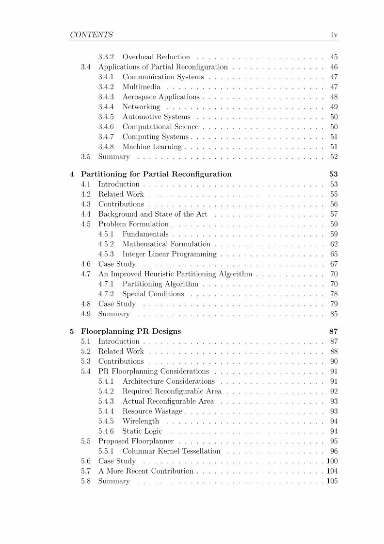
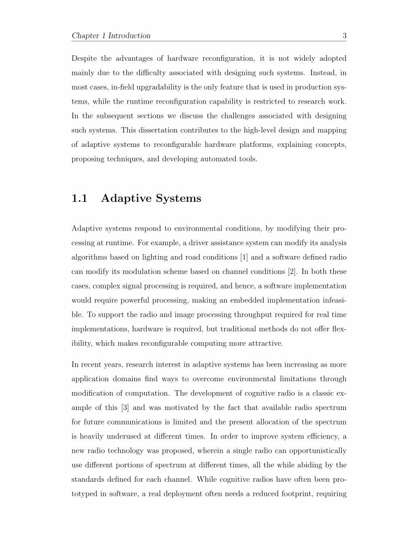
Figure 1.1: Effect of spatial circuit multiplexing on chip size and resourcewastage (a) At time t1, only functions A, B, C and D are active (b) at time t2only functions E, F, G and H are active. Implementing all functions simultane-ously in a single chip requires a larger chip and causes higher resource wastagewhen only a few are active at any point in time. The smaller chip shows that ifonly the required modules could be “loaded” significantly less area is required.
FPGAs started as simple chips, mainly used for glue logic implementations, and
grew to fully-fledged programmable chips capable of implementing complete sys-
tems [4], thanks to the integration of built in hard-macros such as DSP blocks and
BlockRAMs. FPGAs containing hard processors were also released in the early
2000s, but building processor-based systems was hard due to the extensive sup-
porting infrastructure required. More recently, devices such as Xilinx Zynq [5] and
Altera Cyclone V [6] integrate fully functional processor subsystems, including ex-
tensive connectivity and peripherals, making software-hardware co-design easier.
In recent years, FPGAs have been able to successfully challenge dedicated hard-
ware (ASIC) implementations of several systems [7]. This is mainly attributed to
their reprogrammability, increasing logic density, and decreasing cost and power
consumption. For moderate production runs, FPGAs can be more cost effective
compared to ASICs due to the very high non-recurring engineering (NRE) cost
associated with integrated circuit manufacturing processes.
We have discussed how an adaptive system may use different types of processing
in different conditions, and as a result, some functions will be mutually exclusive,
never being required simultaneously. For a traditional hardware design approach,
these functions would all be placed on the chip, with multiplexers used to choose
which is active at any point in time. However, this can significantly increase
area usage if the number of options and mutual exclusivity are high as shown in
Chapter 1 Introduction 6
Fig. 1.1. Larger chips cost more, and consume more power, and since a significant
number of functions may be unused at any point in time, this overhead is wasted.
With FPGAs, we have the option of using the time dimension to overcome this
overhead. The device can be reconfigured to contain only the necessary modules
at any point in time. In this way, a smaller chip, with reduced power consumption
and cost can be used.
1.3 Partial Reconfiguration
Traditionally during an FPGA reconfiguration operation, the entire logic is re-
placed while the device is kept in a reset state. This full reconfiguration allows the
whole datapath to be modified or alternatively for an updated design to be applied
after system deployment. This can also be applied for adaptive systems, where
each possible functional configuration is implemented in a separate bitstream, and
at runtime, the most suitable is chosen and applied through reconfiguration. How-
ever, this requires that the full system pause operation, and a full bitstream to be
loaded, even for small changes. This can consume more time than necessary, and
can break external sensor interfaces, requiring more time for setup and calibration,
though designing and controlling such a system can be easy.
Instead, the approach that is more suited, is what is called partial reconfiguration
(PR), which offers more fine-grained flexibility. PR enables modification of only
portions of the FPGA logic by selectively changing part of the contents of the
configuration memory. Now, the FPGA is no longer required to be kept in reset
mode while being reconfigured making the reconfiguration dynamic in nature. So
portions of the user logic not being configured can continue to execute while the
reconfiguration is in progress.
Although conceptually different, partial reconfiguration and dynamic reconfigura-
tion are frequently interchangeably used in the literature to suggest support for
both. Partial reconfiguration denotes the modification of a portion of the FPGA
logic while the remaining portions are not altered. This operation can be static or

Chapter 1 Introduction 7
dynamic, meaning that the reconfiguration operation can occur while the FPGA
logic is in a reset state (static) or running (dynamic). It is also not necessary
that all dynamic reconfigurations are partial in nature. For example, in context
switching FPGAs, the whole configuration is changed during reconfiguration, but
the operation is dynamic. In this dissertation we use PR to refer to dynamic par-
tial reconfiguration. PR adds an additional dimension to spatial location: time.
With PR, the same portion of the FPGA fabric can serve different functional units
at different time instances. In the context of adaptive systems, this means only the
required functional units need to be reconfigured when the system is reconfigured.
Functional units shared by multiple datapaths can continue to operate without
interruption and the FPGA interface logic never requires reconfiguration.
PR was previously supported on only high-end devices, but is now supported in
all new FPGAs from Xilinx, and some from Altera. PR has remained a constant
research theme within the FPGA community since it was first mentioned nearly
two decades ago. Its major advantages can be summarised as:
• The logic capacity of the FPGA is effectively increased, since several func-
tional units can use the same FPGA resources at different time instances
when their functions are mutually exclusive. This enables use of a smaller
FPGA, reducing overall system cost.
• For some applications, portions of the design remain inactive for long periods
during system operation. Nevertheless, this logic consumes power. Although
techniques such as clock gating can reduce power consumption, parts not
needed can be switched off using PR to further reduce power consumption.
• Since the size of partial bitstreams is often significantly smaller than the full
bitstreams, PR helps to reduce reconfiguration time.
• Using PR, functional units can be selectively reconfigured keeping the re-
maining functional units active and thus the system operational. This capa-
bility is critical for several types of adaptive systems.
Chapter 1 Introduction 8
The primary difficulty with PR is the complex design process. Even for many
experienced FPGA designers, PR remains difficult. It requires expertise in FPGA
architecture, spatial layout, and management of configuration. Hence, its adoption
has been slow.
1.4 Motivations
Adaptive systems on FPGAs are often designed using ad-hoc approaches, where
the system design and implementation are tightly coupled. This results from the
lack of a systematic design methodology, and makes the design complex and hard
to modify. Since the designer has to worry about regions, partial bitstreams, the
reconfiguration operation, and more, all at the lowest implementation levels, they
become embedded deep in the design.
The increasing demand for adaptive systems with real-time performance, and at
the same time the lack of versatile tools for their hardware supported implemen-
tation is our primary motive for this research. Although PR based FPGA designs
are highly suitable for adaptive systems implementation in theory, the design bar-
rier excludes many system designers. In vendor PR tool flows, the designer has to
provide several manual inputs and the efficiency of system implementation greatly
depends upon these. These inputs generally target a specific FPGA architecture,
requiring the system designer to have expertise in FPGA architectures. Similarly
in order to optimise the design, the designer has to know the low level operations
performed during PR. Such an ad-hoc, manual design process is highly time con-
suming and generally leads to sub-optimal results. Target architecture dependency
makes PR an expert feature and makes it less attractive to system level designers.
We feel that the level of abstraction for PR-based adaptive systems design needs
to be increased to a functional level and only minimal architecture-dependent
features should be exposed to the system level designer.
Another important limitation of present PR based systems is the run-time manage-
ment. The particular configurations that the FPGA will operate in, under different
Chapter 1 Introduction 9
environmental conditions, must be explicitly coded by the system designer. This
includes information about specific bitstreams which should be used to configure
the FPGA under different circumstances. This again couples behaviour with spe-
cific implementation and is thus undesirable. Configuration management should
be abstracted, to allow the system designer to focus on the application, not the
implementation. Automated tools should then determine lower level details such
as the bitstreams that need to be configured.
The ideal flow would be for a designer to describe the adaptive system at block
level, using a library of available hardware blocks, then describing, at the same
level, the dynamic behaviour of the system. Tools should then turn this into the
necessary bitstreams and translate the adaptation code at runtime to effect the
necessary configurations. It should then be easy for the designer to test the system
in a PR-enabled testbed that offers the necessary probes and runtime information
to monitor the system’s operation.
The past decade of PR research has mainly focussed on overcoming the limitations
of vendor tools. Most of this work attempts to optimise low level device-specific
features, still requiring architecture expertise. Some high-level tools have been
proposed aiming at task-level time-multiplexing of FPGA resources, but this is
only one way of using PR. There has been limited research in the direction of
exploiting PR at a system level. Research on Run-time management of PR systems
still considers reconfiguration in terms of bitstreams instead of a more abstract
level. While we acknowledge that certain restrictions of the low-level vendor PR
tool flows do limit efficiency to some degree, we see the poor abstraction as a
more urgent issue as it prevents PR from being used by system designers. The
techniques we propose can equally be applied on top of other research design flows,
but we begin with the official flows. In this work we concentrate on Xilinx PR
implementation tools as they are more established and stable. Nevertheless, these
techniques can also be applicable to the Altera PR toolflow as it is similar.

Chapter 1 Introduction 10
1.5 Objectives
The main objectives of this research are to:
1. Demonstrate how an adaptive system can be mapped using PR on an FPGA
and determine the design metrics that influence the quality of the implemen-
tation.
2. Determine how adaptive systems can be described in a way that can be
mapped to real implementations.
3. Develop techniques and tools to automate the PR design process including
partitioning and floorplanning, optimising for PR performance.
4. Develop an abstraction layer to assist design-time and run-time processes
and management of PR systems.
5. Develop a verification platform which enables easier hardware validation of
PR systems.
1.6 Contributions
The main contributions of this work encompass tools, techniques, algorithms and
IP cores developed with focus on enabling easy adoption of PR in adaptive systems
development. These tools and techniques enable system designers who are not
FPGA experts to use PR with relative ease.
1. We have performed a comprehensive study of the partial reconfiguration
process, from both the tools and architectures perspective, including a de-
tailed architecture study of PR capable FPGAs. We have also identified the
metrics associated with PR as well as the limitations of current PR design
flows.

Chapter 1 Introduction 11
2. Efficient partitioning algorithms for PR based adaptive systems have been
developed. The algorithms consider an exact mathematical solution for rel-
atively smaller problems and a novel heuristic algorithm for larger problems.
3. An efficient floorplanning algorithm taking into account both the target
FPGA architecture and factors affecting PR has been developed. The al-
gorithm respects all the constraints imposed by the vendor tool chain and
hence can easily integrate with it.
4. A fully automated PR implementation tool flow has been developed by com-
bining our partitioning, floorplanning and new run-time management tech-
niques with the vendor tool chain. Our tool flow provides an abstract view
of adaptive systems which enables easier system development without delv-
ing into low-level implementation details. Our proposed techniques integrate
with vendor tools rather than circumventing their restrictions which enables
easier adaptation as the FPGA architectures evolve.
5. We have developed a PR evaluation platform, enabling easier hardware val-
idation of PR systems using general purpose computers. The pre-built com-
munication and reconfiguration infrastructure enables faster system devel-
opment and lower verification time.
1.7 Thesis Roadmap
The remainder of this thesis is structured as follows:
Chapter 2 discusses the research background and key objectives guiding this work
and Chapter 3 presents a detailed literature survey on partial reconfiguration
covering architecture, design methodologies, tools, and applications. Chapter 4
presents our exact and heuristic algorithms for automated partitioning for partial
reconfiguration. Chapter 5 discusses automated floorplanning for partial reconfigu-
ration using Columnar kernel tessellation. Chapter 6 discusses PR reconfiguration
management and our custom high-speed reconfiguration controllers. Chapter 7
Chapter 1 Introduction 12
details our fully automated PR development flow targeting hybrid FPGAs. Chap-
ter 8 details our PR hardware evaluation testbed. Finally, Chapter 9 concludes
the work presented and outlines our future research directions.
1.8 Publications
Some of the work presented in this thesis has been written up in a number of
published and submitted papers:
1. K. Vipin and S. A. Fahmy, Efficient Region Allocation for Adaptive Par-
tial Reconfiguration, in Proceedings of the International Conference on Field
Programmable Technology (FPT), New Delhi, 2011.
2. K. Vipin and S. A. Fahmy, Enabling High Level Design of Adaptive Systems
with Partial Reconfiguration, PhD Forum Poster, in Proceedings of the Inter-
national Conference on Field Programmable Technology (FPT), New Delhi,
2011.
3. K. Vipin and S. A. Fahmy, Architecture-Aware Reconfiguration-Centric Floor-
planning for Partial Reconfiguration, in Proceedings of International Sympo-
sium on Applied Reconfigurable Computing (ARC), Hong Kong, 2012, pp.
13–25.
4. K. Vipin and S. A. Fahmy, A High Speed Open Source Controller for FPGA
Partial Reconfiguration, in Proceedings of the International Conference on
Field Programmable Technology (FPT), Seoul, Korea, December 2012, pp.
61-66.
5. K. Vipin and S. A. Fahmy, Automated Partitioning for Partial Reconfig-
uration Design of Adaptive Systems, in Proceedings of the Reconfigurable
Architecture Workshop (RAW), Boston, USA, May 2013, pp. 172-181.

Chapter 1 Introduction 13
6. K. Vipin, S. Shreejith, D. Gunasekara, S. A. Fahmy, and N. Kapre, System-
Level FPGA Device Driver with High-Level Synthesis Support, in Proceed-
ings of the International Conference on Field Programmable Technology
(FPT) , Kyoto, Japan, December 2013, pp. 128-135.
7. K. Vipin and S. A. Fahmy, Automated Partial Reconfiguration Design for
Adaptive Systems with CoPR for Zynq, in Proceedings of the International
Conference on Field Programmable Custom Computing Machines (FCCM),
Boston, Massachusetts, May 2014, pp. 202–205.
8. K. Vipin and S. A. Fahmy, ZyCAP: Efficient Partial Reconfiguration Man-
agement on the Xilinx Zynq, in IEEE Embedded System Letters (ESL), vol.
6, 2014.
9. K. Vipin and S. A. Fahmy, DyRACT: A Partial Reconfiguration Enabled Ac-
celerator and Test Platform, in Proceedings of the International Conference
on Field Programmable Logic and Applications (FPL), Munich, Germany,
September 2014.
1.9 Open Source Releases
1. Reconfiguration controller for Virtex FPGAs. https://github.com/archntu/
prcontrol.
2. ZyCAP: A high performance ICAP controller and run-time PR manager for
Zynq SoCs. https://github.com/archntu/zycap.
3. FPGA Driver: A reusable FPGA design evaluation platform. https://
github.com/vipinkmenon/fpgadriver.
4. Library for PR based video/image processing filters https://github.com/
archntu/dyract/image_lib.
5. PR enabled test and co-processor platform https://github.com/archntu/
dyract.

Chapter 1 Introduction 14
6. Automated PR tool-flow https://github.com/archntu/copr
Chapter 2
Background
Adaptive systems offer the capability to deal with uncertainty in system operating
conditions. An adaptive system can be considered as a collection of different
system operating modes, called configurations, of which only one is active at a
given point in time [8]. At runtime, changes in the operating environment can
cause the system to switch its configuration, called reconfiguration, to adapt to
the conditions. This adaptability can lead to more sophisticated applications as
well as improved performance. Some key application drivers for adaptive systems
include cognitive radios [2], smart camera systems [9], and adaptive security [10].
The flexibility awarded by software programming of a general purpose proces-
sor lends itself well to implementation of adaptive systems, and some frameworks
have been proposed [11]. However, when such systems must interact with the
physical environment, processing large amounts of data, and meeting real time
deadlines, software implementations can fail to deliver. Software adaptive systems
are often implemented on general purpose computers [12], making them unsuit-
able for embedded and portable applications due to their physical size and power
requirements. Instead, we can see that hardware processing could ensure the high-
throughput computation required, while the programmability of FPGAs can also
ensure flexibility is maintained.
15

Chapter 2 Background 16
A
B
C
D
E
F1 0 0
A
B
C
D
E
F0 1 1
(a) (b)
Figure 2.1: Multiplexed hardware system implementation. (a) Datapath useshardware blocks B, C and E by configuring the multiplexes (b) Datapath useshardware blocks A, D and F. The multiplexer control inputs can be managed
through software which configures control registers.
2.1 Hardware Adaptive Systems Implementation
Hardware implementations enable much better application acceleration compared
to software implementations while reducing overall system power consumption
and form factor. Specialised datapaths tailored for specific applications can be
implemented although designing such systems is more difficult.
One limitation generally attributed to hardware implementations is their limited
flexibility. Fixed hardware implementations (ASICs) can not modify their circuitry
once manufactured and a chip redesign demands huge financial investment and
longer turnaround time. This provides FPGAs a new opportunity due to their
re-programmability and lower design time.
To addresses datapath flexibility, both FPGAs and ASICs generally adopt a spatial
multiplexing approach. Here all the required functions (modules) are implemented
in hardware, and multiplexers are used to select between them at runtime. One
benefit of this approach is that designing such a system is comparatively simpler
than more advanced techniques. In fact, the insertion of multiplexers from a high
level description of the block connectivity can be automated. The multiplexer
select lines can be configured using software to select the required functions as
shown in Fig. 2.1. System reconfiguration is also very fast, since the multiplexer
can select between the different datapaths in a matter of clock cycles.
However, this requires all the functional units to be present on the device at
all times, increasing resource utilisation, and possibly requiring a larger FPGA
device than for other approaches. This also leads to increased power consumption.
Chapter 2 Background 17
A1 B3 C2
1 20
A2 B2 C1
3 41
(a) (b)
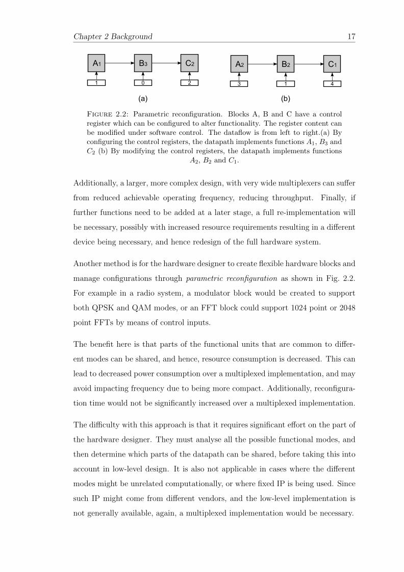
Figure 2.2: Parametric reconfiguration. Blocks A, B and C have a controlregister which can be configured to alter functionality. The register content canbe modified under software control. The dataflow is from left to right.(a) Byconfiguring the control registers, the datapath implements functions A1, B3 andC2 (b) By modifying the control registers, the datapath implements functions
A2, B2 and C1.
Additionally, a larger, more complex design, with very wide multiplexers can suffer
from reduced achievable operating frequency, reducing throughput. Finally, if
further functions need to be added at a later stage, a full re-implementation will
be necessary, possibly with increased resource requirements resulting in a different
device being necessary, and hence redesign of the full hardware system.
Another method is for the hardware designer to create flexible hardware blocks and
manage configurations through parametric reconfiguration as shown in Fig. 2.2.
For example in a radio system, a modulator block would be created to support
both QPSK and QAM modes, or an FFT block could support 1024 point or 2048
point FFTs by means of control inputs.
The benefit here is that parts of the functional units that are common to differ-
ent modes can be shared, and hence, resource consumption is decreased. This can
lead to decreased power consumption over a multiplexed implementation, and may
avoid impacting frequency due to being more compact. Additionally, reconfigura-
tion time would not be significantly increased over a multiplexed implementation.
The difficulty with this approach is that it requires significant effort on the part of
the hardware designer. They must analyse all the possible functional modes, and
then determine which parts of the datapath can be shared, before taking this into
account in low-level design. It is also not applicable in cases where the different
modes might be unrelated computationally, or where fixed IP is being used. Since
such IP might come from different vendors, and the low-level implementation is
not generally available, again, a multiplexed implementation would be necessary.
Chapter 2 Background 18
Region 1
FPGA fabric
Region 2
A1
A2
B2B1
B3
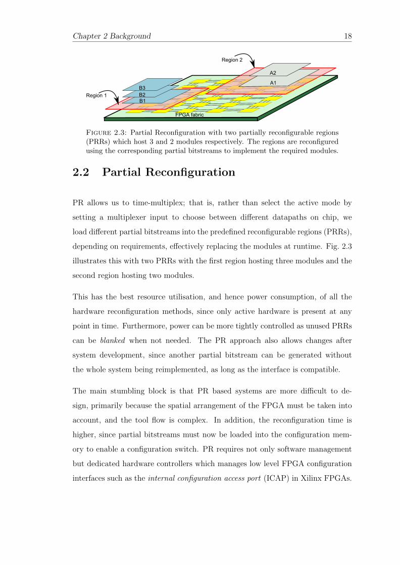
Figure 2.3: Partial Reconfiguration with two partially reconfigurable regions(PRRs) which host 3 and 2 modules respectively. The regions are reconfiguredusing the corresponding partial bitstreams to implement the required modules.
2.2 Partial Reconfiguration
PR allows us to time-multiplex; that is, rather than select the active mode by
setting a multiplexer input to choose between different datapaths on chip, we
load different partial bitstreams into the predefined reconfigurable regions (PRRs),
depending on requirements, effectively replacing the modules at runtime. Fig. 2.3
illustrates this with two PRRs with the first region hosting three modules and the
second region hosting two modules.
This has the best resource utilisation, and hence power consumption, of all the
hardware reconfiguration methods, since only active hardware is present at any
point in time. Furthermore, power can be more tightly controlled as unused PRRs
can be blanked when not needed. The PR approach also allows changes after
system development, since another partial bitstream can be generated without
the whole system being reimplemented, as long as the interface is compatible.
The main stumbling block is that PR based systems are more difficult to de-
sign, primarily because the spatial arrangement of the FPGA must be taken into
account, and the tool flow is complex. In addition, the reconfiguration time is
higher, since partial bitstreams must now be loaded into the configuration mem-
ory to enable a configuration switch. PR requires not only software management
but dedicated hardware controllers which manages low level FPGA configuration
interfaces such as the internal configuration access port (ICAP) in Xilinx FPGAs.
Chapter 2 Background 19
Region 1
FPGA fabric
Region 2
A1
A2 B2
B1
(a)
Single Region
FPGA fabric
A1 B2
B1A2
(b)
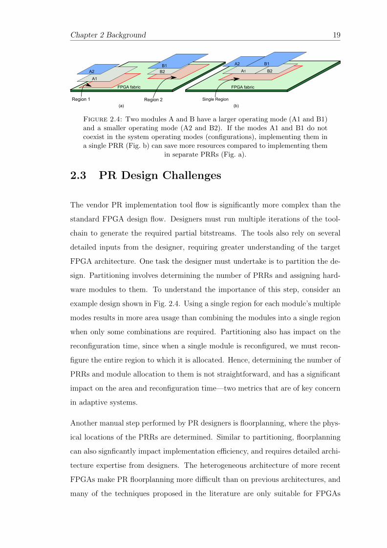
Figure 2.4: Two modules A and B have a larger operating mode (A1 and B1)and a smaller operating mode (A2 and B2). If the modes A1 and B1 do notcoexist in the system operating modes (configurations), implementing them ina single PRR (Fig. b) can save more resources compared to implementing them
in separate PRRs (Fig. a).
2.3 PR Design Challenges
The vendor PR implementation tool flow is significantly more complex than the
standard FPGA design flow. Designers must run multiple iterations of the tool-
chain to generate the required partial bitstreams. The tools also rely on several
detailed inputs from the designer, requiring greater understanding of the target
FPGA architecture. One task the designer must undertake is to partition the de-
sign. Partitioning involves determining the number of PRRs and assigning hard-
ware modules to them. To understand the importance of this step, consider an
example design shown in Fig. 2.4. Using a single region for each module’s multiple
modes results in more area usage than combining the modules into a single region
when only some combinations are required. Partitioning also has impact on the
reconfiguration time, since when a single module is reconfigured, we must recon-
figure the entire region to which it is allocated. Hence, determining the number of
PRRs and module allocation to them is not straightforward, and has a significant
impact on the area and reconfiguration time—two metrics that are of key concern
in adaptive systems.
Another manual step performed by PR designers is floorplanning, where the phys-
ical locations of the PRRs are determined. Similar to partitioning, floorplanning
can also signficantly impact implementation efficiency, and requires detailed archi-
tecture expertise from designers. The heterogeneous architecture of more recent
FPGAs make PR floorplanning more difficult than on previous architectures, and
many of the techniques proposed in the literature are only suitable for FPGAs
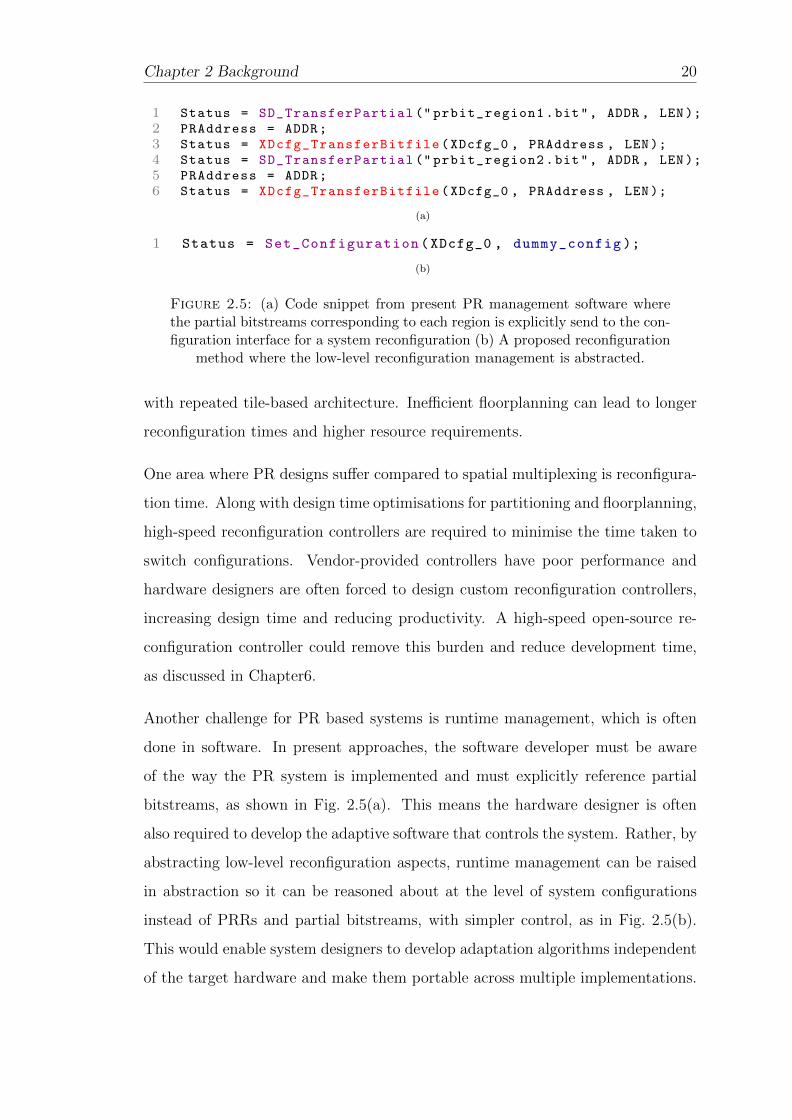
Chapter 2 Background 20
1 Status = SD_TransferPartial (" prbit_region1.bit", ADDR , LEN);2 PRAddress = ADDR;3 Status = XDcfg_TransferBitfile(XDcfg_0 , PRAddress , LEN);4 Status = SD_TransferPartial (" prbit_region2.bit", ADDR , LEN);5 PRAddress = ADDR;6 Status = XDcfg_TransferBitfile(XDcfg_0 , PRAddress , LEN);
(a)
1 Status = Set_Configuration(XDcfg_0 , dummy_config );
(b)
Figure 2.5: (a) Code snippet from present PR management software wherethe partial bitstreams corresponding to each region is explicitly send to the con-figuration interface for a system reconfiguration (b) A proposed reconfiguration
method where the low-level reconfiguration management is abstracted.
with repeated tile-based architecture. Inefficient floorplanning can lead to longer
reconfiguration times and higher resource requirements.
One area where PR designs suffer compared to spatial multiplexing is reconfigura-
tion time. Along with design time optimisations for partitioning and floorplanning,
high-speed reconfiguration controllers are required to minimise the time taken to
switch configurations. Vendor-provided controllers have poor performance and
hardware designers are often forced to design custom reconfiguration controllers,
increasing design time and reducing productivity. A high-speed open-source re-
configuration controller could remove this burden and reduce development time,
as discussed in Chapter6.
Another challenge for PR based systems is runtime management, which is often
done in software. In present approaches, the software developer must be aware
of the way the PR system is implemented and must explicitly reference partial
bitstreams, as shown in Fig. 2.5(a). This means the hardware designer is often
also required to develop the adaptive software that controls the system. Rather, by
abstracting low-level reconfiguration aspects, runtime management can be raised
in abstraction so it can be reasoned about at the level of system configurations
instead of PRRs and partial bitstreams, with simpler control, as in Fig. 2.5(b).
This would enable system designers to develop adaptation algorithms independent
of the target hardware and make them portable across multiple implementations.
Chapter 2 Background 21
2.4 Summary
Adaptation is becoming more important in a wide variety of application domains,
but software implementations on processors do not offer the required performance
when dealing with complex data and algorithms. Partial reconfiguration of FPGAs
is a promising technique for implementing such systems, since it combines some
of the performance of a custom hardware implementation with some flexibility
to support adaptation. The present PR design flow is, however, insufficiently
automated and relies on several detailed inputs from the designer, requiring low-
level FPGA architecture expertise. Run-time management of such systems is also
typically done at a very low level that fails to abstract the PR details from the
adaptation programmer. Tools that automate and provide an abstract view of
adaptation can make PR more attractive for adaptive systems designers who are
not hardware experts. Our hope is that our work will spur more widespread use
of PR, and hence improvements in providers’ design flows.

Chapter 3
Review of Literature
In this chapter, we review the development of dynamic and partial reconfiguration
techniques over the years and the current state of the art in the area. We analyse
different aspects of PR including device architectures, design frameworks, PR
development tools, optimisation strategies, and applications.
3.1 Architecture
Conceptually all FPGA devices can be considered as being composed of two dis-
tinct layers: the configuration memory layer and the hardware logic layer [13]
as shown in Fig. 3.1. FPGAs achieve their unique re-programmability and flex-
ibility due to this composition. The hardware logic layer contains the hardware
resources of the FPGA, including lookup tables (LUTs), flip-flops, DSP blocks,
memory blocks, transceivers, and others. This layer also contains the routing
resources and switch boxes that allow components to be connected.
The configuration memory layer stores the FPGA configuration information, usu-
ally called a bitstream. This bitstream contains all the information that determines
the implemented circuit, such as the values stored in the LUTs, initial set and re-
set status of flip-flops, initialisation values for memories, standards of the input
and output pins, and the routing information for the programmable interconnect.
22
Chapter 3 Review of Literature 23
LUT
LUT
FF
FF
CONFIGURATION MEMORY
HARDWARE LAYER
ROUTING RESOURCES
LOGIC RESOURCES
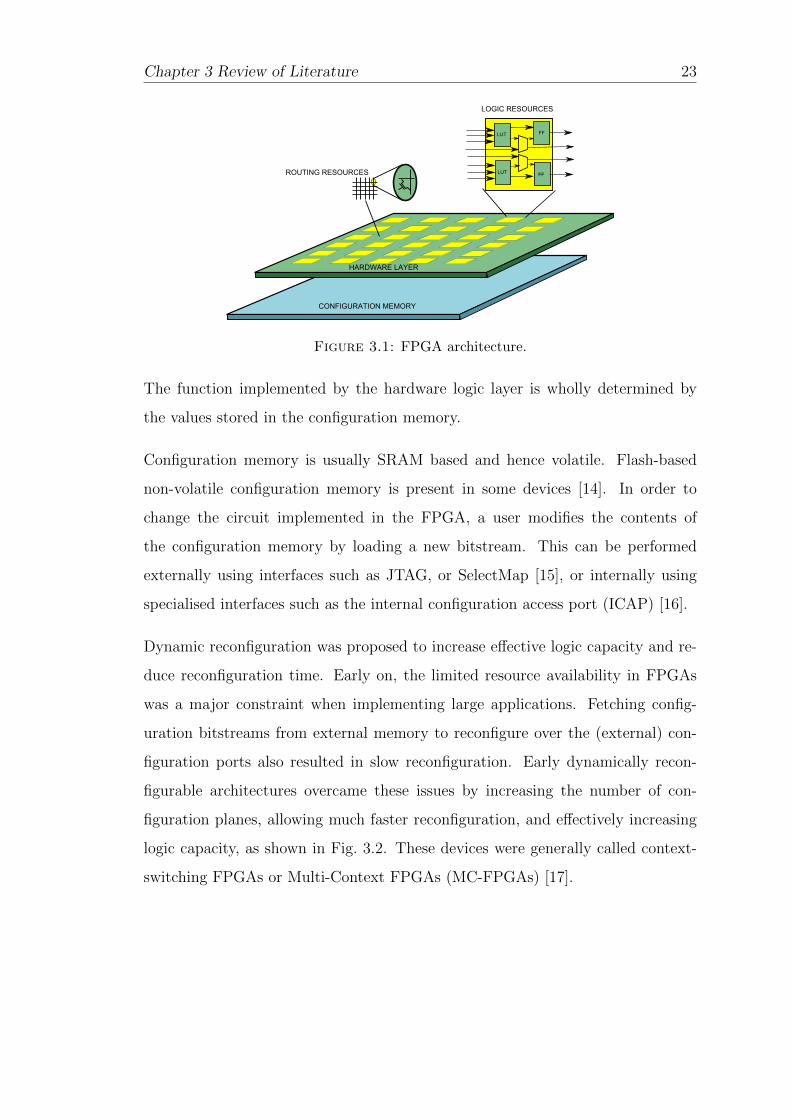
Figure 3.1: FPGA architecture.
The function implemented by the hardware logic layer is wholly determined by
the values stored in the configuration memory.
Configuration memory is usually SRAM based and hence volatile. Flash-based
non-volatile configuration memory is present in some devices [14]. In order to
change the circuit implemented in the FPGA, a user modifies the contents of
the configuration memory by loading a new bitstream. This can be performed
externally using interfaces such as JTAG, or SelectMap [15], or internally using
specialised interfaces such as the internal configuration access port (ICAP) [16].
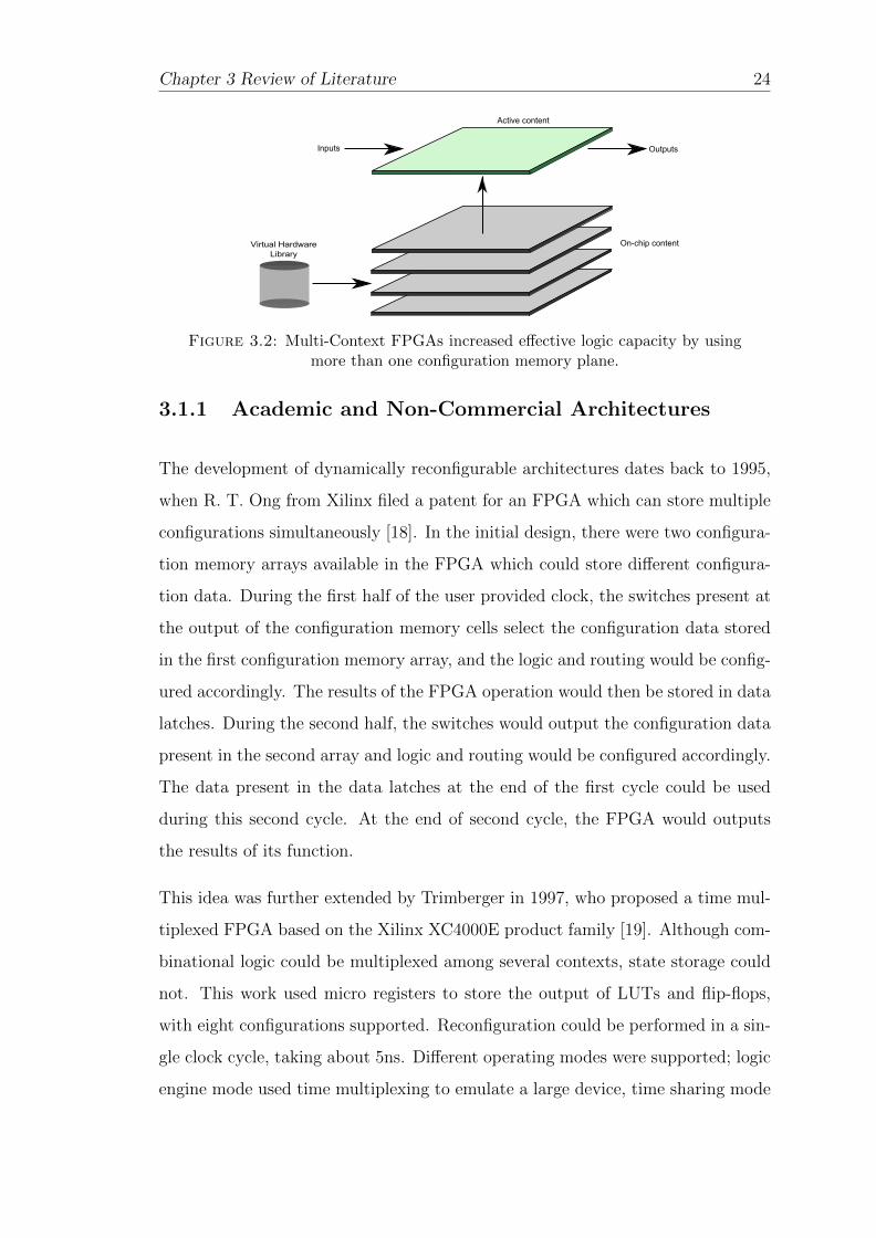
Dynamic reconfiguration was proposed to increase effective logic capacity and re-
duce reconfiguration time. Early on, the limited resource availability in FPGAs
was a major constraint when implementing large applications. Fetching config-
uration bitstreams from external memory to reconfigure over the (external) con-
figuration ports also resulted in slow reconfiguration. Early dynamically recon-
figurable architectures overcame these issues by increasing the number of con-
figuration planes, allowing much faster reconfiguration, and effectively increasing
logic capacity, as shown in Fig. 3.2. These devices were generally called context-
switching FPGAs or Multi-Context FPGAs (MC-FPGAs) [17].
Chapter 3 Review of Literature 24
Virtual HardwareLibrary
Inputs Outputs
Active content
On-chip content
Figure 3.2: Multi-Context FPGAs increased effective logic capacity by usingmore than one configuration memory plane.
3.1.1 Academic and Non-Commercial Architectures
The development of dynamically reconfigurable architectures dates back to 1995,
when R. T. Ong from Xilinx filed a patent for an FPGA which can store multiple
configurations simultaneously [18]. In the initial design, there were two configura-
tion memory arrays available in the FPGA which could store different configura-
tion data. During the first half of the user provided clock, the switches present at
the output of the configuration memory cells select the configuration data stored
in the first configuration memory array, and the logic and routing would be config-
ured accordingly. The results of the FPGA operation would then be stored in data
latches. During the second half, the switches would output the configuration data
present in the second array and logic and routing would be configured accordingly.
The data present in the data latches at the end of the first cycle could be used
during this second cycle. At the end of second cycle, the FPGA would outputs
the results of its function.
This idea was further extended by Trimberger in 1997, who proposed a time mul-
tiplexed FPGA based on the Xilinx XC4000E product family [19]. Although com-
binational logic could be multiplexed among several contexts, state storage could
not. This work used micro registers to store the output of LUTs and flip-flops,
with eight configurations supported. Reconfiguration could be performed in a sin-
gle clock cycle, taking about 5ns. Different operating modes were supported; logic
engine mode used time multiplexing to emulate a large device, time sharing mode
Chapter 3 Review of Literature 25
emulated a number of independent FPGAs, and static mode stored the same con-
figuration data in different configuration planes, as well as a mix of these modes.
An inactive configuration plane could be modified at runtime by loading configu-
ration data from off-chip storage. A special “RAM” mode allowed user designs to
read and write to the configuration memory directly, allowing for self-modifying
hardware.
The main drawback of MC-FPGA architectures is their high power consumption.
Due to a large number of configuration bits and high switching activity, the power
consumption of these devices was in the tens of Watts for an average design running
at 40MHz, making them unsuitable for many applications. Chong et al. proposed
the reconfigurable context memory (RCM) to tackle the area and power overheads
of MC-FPGAs [17]. RCM exploits the redundancy and regularity in configuration
bits between different contexts. Their approach leverages a previous study which
showed that during context switching, less than 3% of the configuration data was
modified [20]. Additionally ferroelectric-based functional pass-gates are used in
RCM to achieve compactness and lower power. Their design claimed to reduce
the FPGA area to 37% of other MC-FPGAs and consume much lesser power.
One of the major restrictions for adopting MC-FPGAs was the lack of design
automation (EDA) tools, which could efficiently map applications to these plat-
forms. Designs had to be manually partitioned into multiple segments and mapped
to different contexts.
Another early architecture proposed to support dynamic reconfiguration was the
Dynamically Programmable Gate Array (DPGA) [21]. DPGAs used traditional
4 input LUTs as the basic logic element, but each LUT and interconnect cell
had an associated 4-context memory implemented using DRAM. DPGAs were
mainly motivated by slow off-chip configuration loading which would take several
milliseconds to complete. DPGAs supported different usage models with multiple
independent functions in different configurations [22]. They supported temporal
pipelining, where multiple contexts are used to implement a single function by
time multiplexing. The prototypes developed had limited logic capacity, operating
Chapter 3 Review of Literature 26
ROM(LUT)
RAM(LUT)
FFDENQ
Figure 3.3: CSLC architecture.
frequency and a lack of automation tools. Using DRAM for configuration memory
also enforced a minimum operating frequency of 5MHz due to DRAM refresh
requirements.
The first practical context switching FPGA was developed by researchers at Sanders,
a Lockheed Martin company, on a 0.35µm process [23]. The device was called a
Context Switching Reconfigurable Computer (CSRC), and could store up to four
configurations concurrently. The device was composed of 16-bit wide data pipes
with each pipe composed of context switching logic arrays (CSLAs). Each CSLA
could process two 16-bit words and each CSLA was connected to two adjacent
CSLAs which made it possible to transfer data in both directions. The architec-
ture used three levels of routing for data to flow from any CSLA to any other
CSLA. Each CSLA was composed of 16 context switching logic cells (CSLCs) as
shown in Fig. 3.3. Each CSLC contained a four input lookup table, carry logic,
a context switching flip-flop and a tri-state buffer. A separate context switching
RAM was used for storage. Each configurable resource, along with the routing,
was controlled by four configuration bits, of which one bit was active at any point
in time, thus implementing four configurable planes. The limited routing architec-
ture of this device made implementation of some applications impossible on this
architecture.
GARP was another dynamically reconfigurable architecture, that combined re-
configurable hardware with a standard MIPS processor [24]. The reconfigurable
fabric was a slave computational unit located on the same die as the processor.
Chapter 3 Review of Literature 27
Loading and execution on the reconfigurable array was controlled by a programme
running on the processor. The standard memory hierarchy of the processor was
also accessible to the reconfigurable fabric. The reconfigurable array was divided
into blocks and one block in each row was called a control block, with others called
logic blocks. The processor enabled an array by setting a clock counter. When
the clock counter reached zero, array execution would stop and the results would
be copied by the processor. GARP allowed partial array configuration down to
individual rows. A physical implementation of GARP was never made available
for practical use.
3.1.2 Commercial Devices Supporting PR
Among the major vendors, Xilinx’s FPGAs are the most popular devices support-
ing PR, as they have done for years. The first Xilinx FPGA to support partial
reconfiguration was the XC6200 series [25]. This device supported true dynamic
partial reconfiguration, allowing only a portion of the FPGA to be reconfigured
while the remaining portions continue functioning. This device contained only a
single configurable memory plane. Using a special interface, an external processor
could access any specific logic cell in the FPGA, and modify its configuration, with
the configuration SRAM mapped to the processor address space. Due to a regular
structure with every cell and its associated routing being similar, reconfiguration
was simpler with these devices than for modern ones. Recent FPGAs have highly
heterogeneous architectures and complex routing structures.
PR became more popular with the introduction of the Virtex-II [26] and Virtex-II
Pro [27] series of FPGAs from Xilinx. These FPGAs included built-in hard macros
such as Block RAMs and 18×18 embedded multipliers, for efficient implementation
of more complex circuits. It was possible to load new data to the configuration
memory while the remaining portions of the design continued to execute. A partial
bitstream could be loaded externally using the SelectMap or JTAG interfaces. In
Virtex devices, Xilinx introduced a new configuration interface called the Internal
Configuration Access Port (ICAP). This made it possible to load bitstreams from

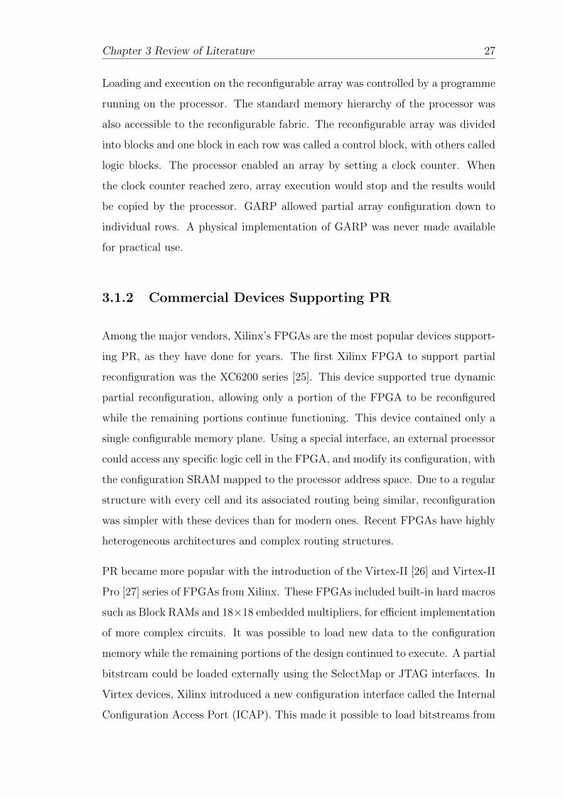
Chapter 3 Review of Literature 28
User IOs
User IOs
User IO
sUse
r IO
s
16 X 16 Tile
4 X 4 Block
Functional Cell
Functional Unit
Figure 3.4: Xilinx XC6200 architecture.
within the FPGA fabric. A soft-processor or a custom state machine could fetch
configuration information from external memory and write to the configuration
memory through the ICAP.
In these devices, the configuration memory is organised in frames [28], with a
frame being the smallest unit of configuration, 1-bit wide and extending the whole
height of the device – hence the size of a frame is device dependent. A configuration
frame does not map to any single hardware resource, but it configures a narrow
vertical slice of many physical resources. Configuration frames are grouped into
six different configuration columns depending upon their hardware-mapping called
IOB, IOI, CLB, GCLK, BlockRAM, and BlockRAM Interconnect. IOB columns
are used for configuring the voltage standard for the I/Os. The CLB columns
program the configurable logic blocks, routing, and most interconnect. BlockRAM
configuration columns are used for programming the BlockRAM user memory
space.
For these devices, there are several restrictions on the size and shape of partial
reconfiguration regions (PRRs). They should extend the full height of the device
and, horizontally, they should align with a four slice boundary. These restrictions
can make a design inefficient in terms of hardware utilisation, but floorplanning the
regions is relatively simple. Tri-state buffers (TBUFs) have to be placed between
reconfigurable regions and the static region in order to manage the connectivity
between them.
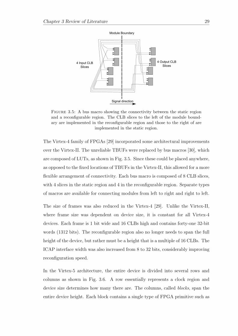
Chapter 3 Review of Literature 29
Module Boundary
Signal direction
4 Input CLBSlices
4 Output CLBSlices
Figure 3.5: A bus macro showing the connectivity between the static regionand a reconfigurable region. The CLB slices to the left of the module bound-ary are implemented in the reconfigurable region and those to the right of are
implemented in the static region.
The Virtex-4 family of FPGAs [29] incorporated some architectural improvements
over the Virtex-II. The unreliable TBUFs were replaced by bus macros [30], which
are composed of LUTs, as shown in Fig. 3.5. Since these could be placed anywhere,
as opposed to the fixed locations of TBUFs in the Virtex-II, this allowed for a more
flexible arrangement of connectivity. Each bus macro is composed of 8 CLB slices,
with 4 slices in the static region and 4 in the reconfigurable region. Separate types
of macros are available for connecting modules from left to right and right to left.
The size of frames was also reduced in the Virtex-4 [29]. Unlike the Virtex-II,
where frame size was dependent on device size, it is constant for all Virtex-4
devices. Each frame is 1 bit wide and 16 CLBs high and contains forty-one 32-bit
words (1312 bits). The reconfigurable region also no longer needs to span the full
height of the device, but rather must be a height that is a multiple of 16 CLBs. The
ICAP interface width was also increased from 8 to 32 bits, considerably improving
reconfiguration speed.
In the Virtex-5 architecture, the entire device is divided into several rows and
columns as shown in Fig. 3.6. A row essentially represents a clock region and
device size determines how many there are. The columns, called blocks, span the
entire device height. Each block contains a single type of FPGA primitive such as
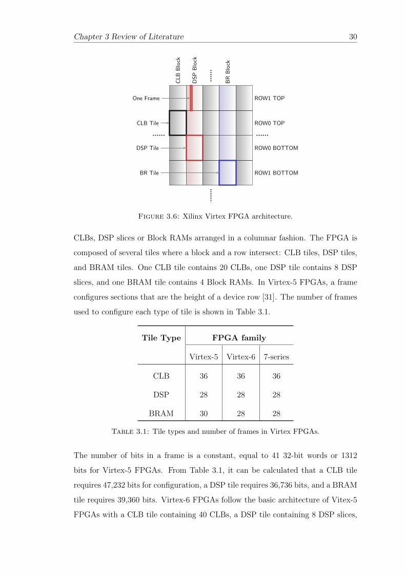
Chapter 3 Review of Literature 30
CLB Tile
DSP Tile
BR Tile
One Frame
CLBBlock
DSPBlock
BRBlock
ROW1 TOP
ROW0 TOP
ROW0 BOTTOM
ROW1 BOTTOM
Figure 3.6: Xilinx Virtex FPGA architecture.
CLBs, DSP slices or Block RAMs arranged in a columnar fashion. The FPGA is
composed of several tiles where a block and a row intersect: CLB tiles, DSP tiles,
and BRAM tiles. One CLB tile contains 20 CLBs, one DSP tile contains 8 DSP
slices, and one BRAM tile contains 4 Block RAMs. In Virtex-5 FPGAs, a frame
configures sections that are the height of a device row [31]. The number of frames
used to configure each type of tile is shown in Table 3.1.
Tile Type FPGA family
Virtex-5 Virtex-6 7-series
CLB 36 36 36
DSP 28 28 28
BRAM 30 28 28
Table 3.1: Tile types and number of frames in Virtex FPGAs.
The number of bits in a frame is a constant, equal to 41 32-bit words or 1312
bits for Virtex-5 FPGAs. From Table 3.1, it can be calculated that a CLB tile
requires 47,232 bits for configuration, a DSP tile requires 36,736 bits, and a BRAM
tile requires 39,360 bits. Virtex-6 FPGAs follow the basic architecture of Vitex-5
FPGAs with a CLB tile containing 40 CLBs, a DSP tile containing 8 DSP slices,
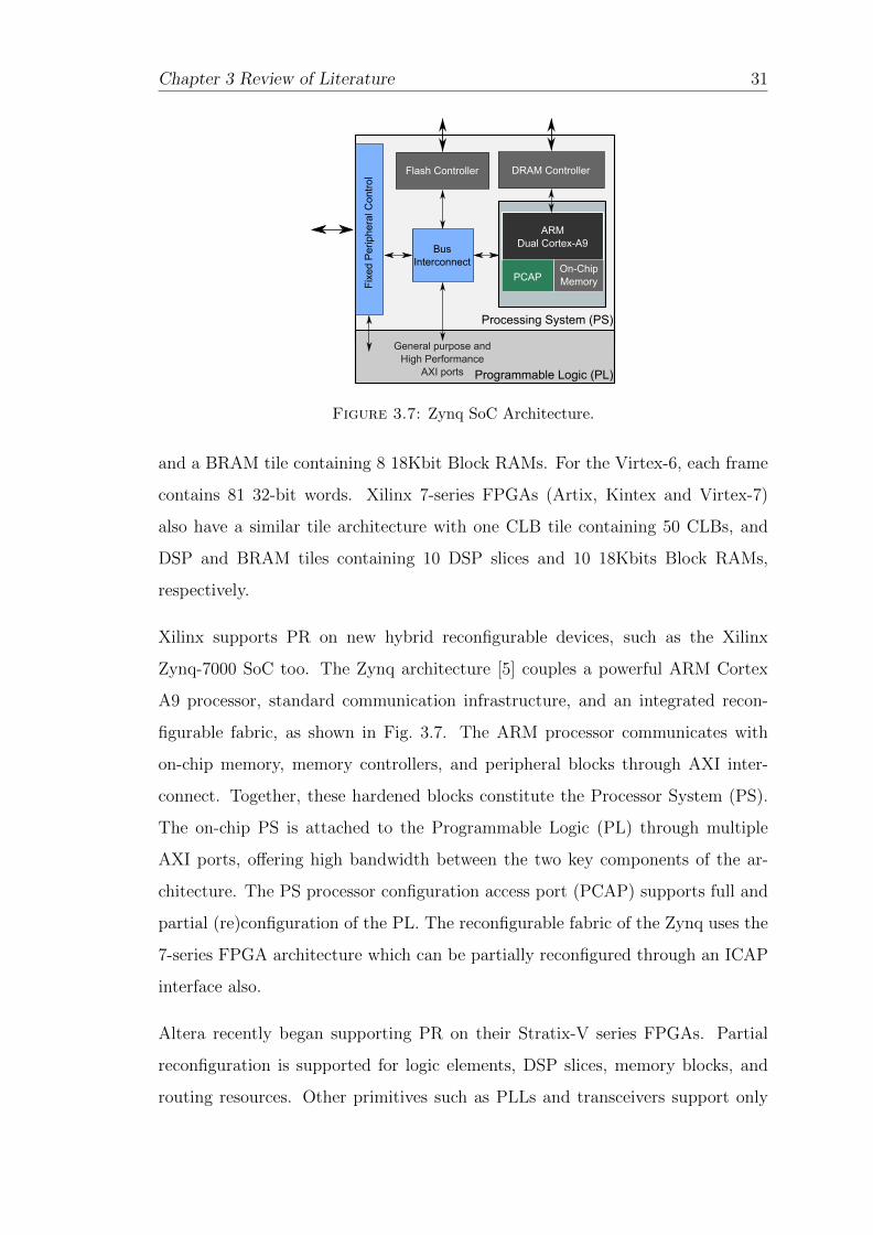
Chapter 3 Review of Literature 31
Fix
ed P
erip
hera
l Con
trol
ARM Dual Cortex-A9
On-ChipMemory
PCAP
Programmable Logic (PL)
General purpose and High Performance
AXI ports
DRAM Controller
Processing System (PS)
Bus Interconnect
Flash Controller
Figure 3.7: Zynq SoC Architecture.
and a BRAM tile containing 8 18Kbit Block RAMs. For the Virtex-6, each frame
contains 81 32-bit words. Xilinx 7-series FPGAs (Artix, Kintex and Virtex-7)
also have a similar tile architecture with one CLB tile containing 50 CLBs, and
DSP and BRAM tiles containing 10 DSP slices and 10 18Kbits Block RAMs,
respectively.
Xilinx supports PR on new hybrid reconfigurable devices, such as the Xilinx
Zynq-7000 SoC too. The Zynq architecture [5] couples a powerful ARM Cortex
A9 processor, standard communication infrastructure, and an integrated recon-
figurable fabric, as shown in Fig. 3.7. The ARM processor communicates with
on-chip memory, memory controllers, and peripheral blocks through AXI inter-
connect. Together, these hardened blocks constitute the Processor System (PS).
The on-chip PS is attached to the Programmable Logic (PL) through multiple
AXI ports, offering high bandwidth between the two key components of the ar-
chitecture. The PS processor configuration access port (PCAP) supports full and
partial (re)configuration of the PL. The reconfigurable fabric of the Zynq uses the
7-series FPGA architecture which can be partially reconfigured through an ICAP
interface also.
Altera recently began supporting PR on their Stratix-V series FPGAs. Partial
reconfiguration is supported for logic elements, DSP slices, memory blocks, and
routing resources. Other primitives such as PLLs and transceivers support only
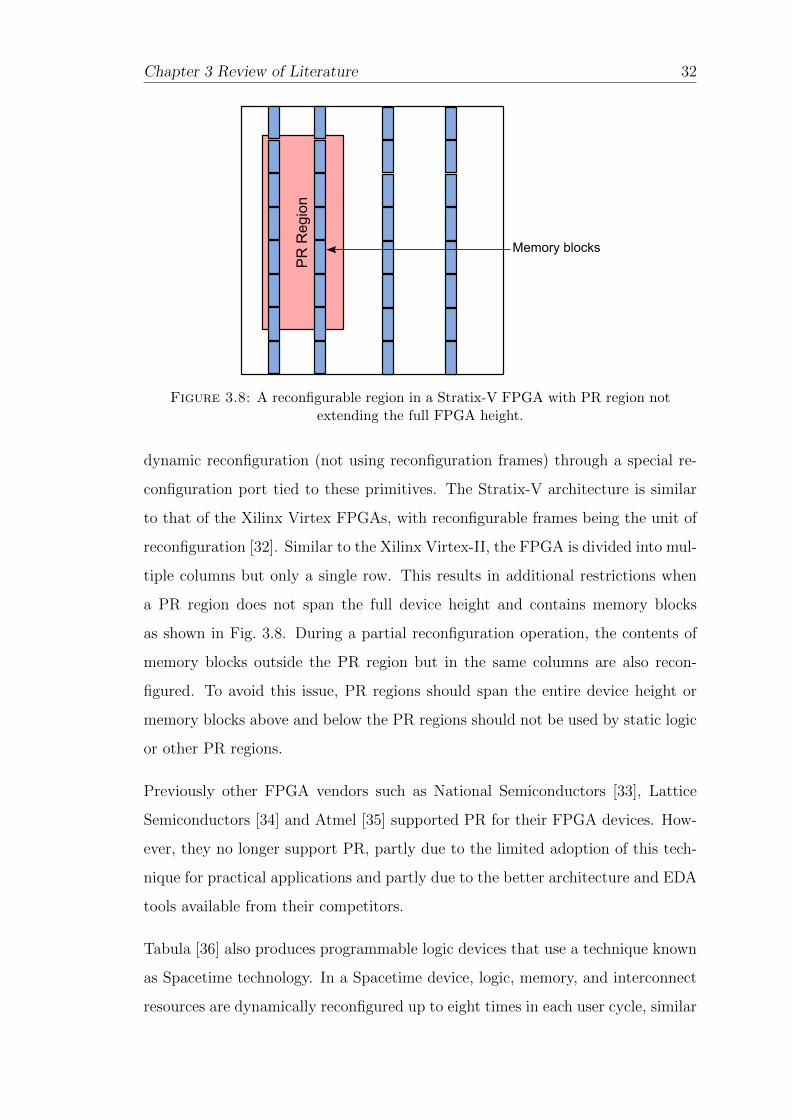
Chapter 3 Review of Literature 32
PR
Reg
ion
Memory blocks
Figure 3.8: A reconfigurable region in a Stratix-V FPGA with PR region notextending the full FPGA height.
dynamic reconfiguration (not using reconfiguration frames) through a special re-
configuration port tied to these primitives. The Stratix-V architecture is similar
to that of the Xilinx Virtex FPGAs, with reconfigurable frames being the unit of
reconfiguration [32]. Similar to the Xilinx Virtex-II, the FPGA is divided into mul-
tiple columns but only a single row. This results in additional restrictions when
a PR region does not span the full device height and contains memory blocks
as shown in Fig. 3.8. During a partial reconfiguration operation, the contents of
memory blocks outside the PR region but in the same columns are also recon-
figured. To avoid this issue, PR regions should span the entire device height or
memory blocks above and below the PR regions should not be used by static logic
or other PR regions.
Previously other FPGA vendors such as National Semiconductors [33], Lattice
Semiconductors [34] and Atmel [35] supported PR for their FPGA devices. How-
ever, they no longer support PR, partly due to the limited adoption of this tech-
nique for practical applications and partly due to the better architecture and EDA
tools available from their competitors.
Tabula [36] also produces programmable logic devices that use a technique known
as Spacetime technology. In a Spacetime device, logic, memory, and interconnect
resources are dynamically reconfigured up to eight times in each user cycle, similar
Chapter 3 Review of Literature 33
to context-switching FPGAs. The Spacetime compiler automatically maps, places,
and routes a user design into the device using standard VHDL/Verilog inputs and
flows. To enable rapid reconfiguration, configuration data is stored locally beside
the resources it controls and this local configuration memory appears like a stack.
As each configuration is read from the top of the stack, the next configuration rises
to the top, and the current configuration goes to the bottom of the stack, with
the process repeating continuously. A major limiting factor of previous context-
switching FPGAs was their power consumption. Tabula claims to have overcome
this through new manufacturing techniques, however, exact power consumption
measurements for these devices are not yet available in the literature.
3.2 Design Methodologies
In this section we review the design methodologies for PR systems and the sup-
porting tools developed to simplify system implementation. We will review design
methods from both industry and the research community.
3.2.1 Vendor PR Design Flows
The first major FPGA vendor to support PR was Xilinx, with the introduction of
the Virtex-II in 2003 [26]. Altera announced support for PR from their Stratix-V
series FPGAs onwards [37]. The tool flow offered by both vendors is similar with
slight differences arising due to the different architectures.
3.2.1.1 Xilinx PR Flow
Xilinx supports PR through a hierarchical module-based design tool called PlanA-
head [38]. Each PR design is composed of number of modules, or functional units,
for example a filter. All modules are described using a hardware description lan-
guage (HDL) or can be pre-synthesised netlists.
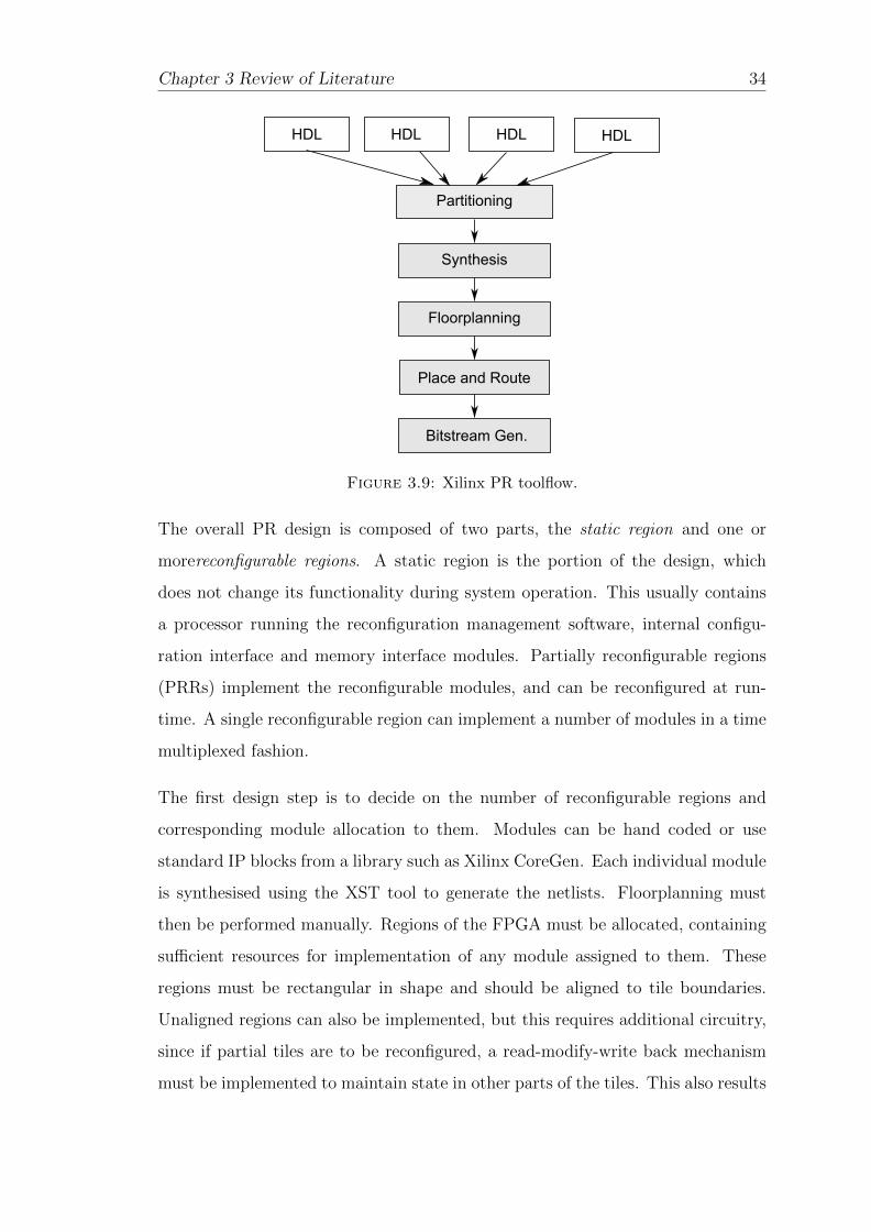
Chapter 3 Review of Literature 34
HDL HDL HDL HDL
Partitioning
Synthesis
Floorplanning
Place and Route
Bitstream Gen.
Figure 3.9: Xilinx PR toolflow.
The overall PR design is composed of two parts, the static region and one or
morereconfigurable regions. A static region is the portion of the design, which
does not change its functionality during system operation. This usually contains
a processor running the reconfiguration management software, internal configu-
ration interface and memory interface modules. Partially reconfigurable regions
(PRRs) implement the reconfigurable modules, and can be reconfigured at run-
time. A single reconfigurable region can implement a number of modules in a time
multiplexed fashion.
The first design step is to decide on the number of reconfigurable regions and
corresponding module allocation to them. Modules can be hand coded or use
standard IP blocks from a library such as Xilinx CoreGen. Each individual module
is synthesised using the XST tool to generate the netlists. Floorplanning must
then be performed manually. Regions of the FPGA must be allocated, containing
sufficient resources for implementation of any module assigned to them. These
regions must be rectangular in shape and should be aligned to tile boundaries.
Unaligned regions can also be implemented, but this requires additional circuitry,
since if partial tiles are to be reconfigured, a read-modify-write back mechanism
must be implemented to maintain state in other parts of the tiles. This also results
Chapter 3 Review of Literature 35
in higher reconfiguration time. Hence, generally tiles are not shared between
reconfigurable regions.
The designer then works out the combinations of the modules required for data
processing, where each valid combination is called a configuration. Finally the
tools generate a full reconfiguration bitstream as well as partial bitstreams for
each reconfigurable region, for each configuration. To help meet timing, the con-
figuration with highest resource consumption is implemented first and the routing
is preserved in the subsequent implementations. The implementation tools auto-
matically insert bus macros to preserve the routing between the static logic and
PR regions.
Xilinx previously offered a difference-based partial reconfiguration flow [39]. This
allowed small changes, by editing a design using the FPGA Editor software. Im-
plementation tools would then generate a partial bitstream containing only the
difference between the new and old designs. This flow is no longer supported for
PR designs.
To manage FPGA reconfiguration at run-time using the generated partial bit-
streams, the designer typically includes a processor to control the process, and
writes software code specifying the different conditions under which reconfigu-
ration should happen and the specific bitstream for each PRR which should be
reconfigured. This means the software developer must be aware of how the de-
sign is partitioned and which bitstreams correspond to each region for different
configurations.
3.2.1.2 Altera PR Flow
The Altera PR flow is supported through their Quartus-II software [40]. Altera
refer to programming frames and call configurations revisions. Module variations
implemented in the same PR region are called personas.
Two different PR implementation schemes are possible, depending on the arrange-
ment of reconfigurable regions. The SCRUB mode is used when programming
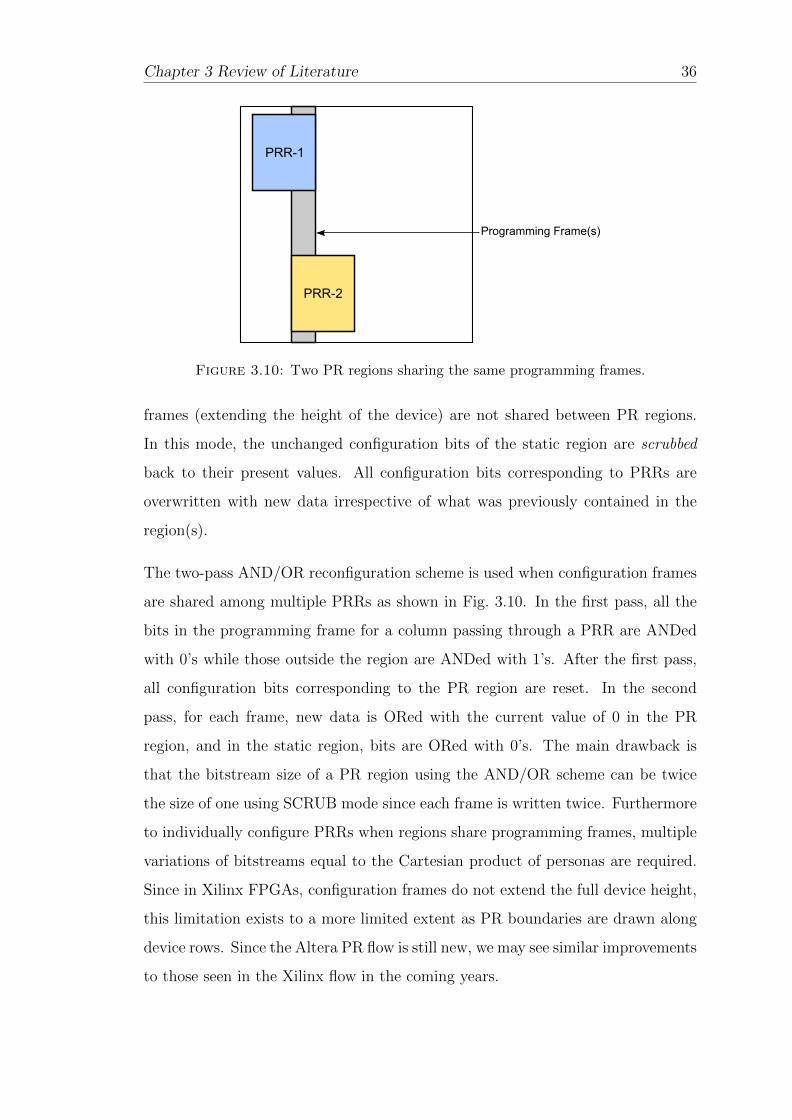
Chapter 3 Review of Literature 36
Programming Frame(s)
PRR-1
PRR-2
Figure 3.10: Two PR regions sharing the same programming frames.
frames (extending the height of the device) are not shared between PR regions.
In this mode, the unchanged configuration bits of the static region are scrubbed
back to their present values. All configuration bits corresponding to PRRs are
overwritten with new data irrespective of what was previously contained in the
region(s).
The two-pass AND/OR reconfiguration scheme is used when configuration frames
are shared among multiple PRRs as shown in Fig. 3.10. In the first pass, all the
bits in the programming frame for a column passing through a PRR are ANDed
with 0’s while those outside the region are ANDed with 1’s. After the first pass,
all configuration bits corresponding to the PR region are reset. In the second
pass, for each frame, new data is ORed with the current value of 0 in the PR
region, and in the static region, bits are ORed with 0’s. The main drawback is
that the bitstream size of a PR region using the AND/OR scheme can be twice
the size of one using SCRUB mode since each frame is written twice. Furthermore
to individually configure PRRs when regions share programming frames, multiple
variations of bitstreams equal to the Cartesian product of personas are required.
Since in Xilinx FPGAs, configuration frames do not extend the full device height,
this limitation exists to a more limited extent as PR boundaries are drawn along
device rows. Since the Altera PR flow is still new, we may see similar improvements
to those seen in the Xilinx flow in the coming years.
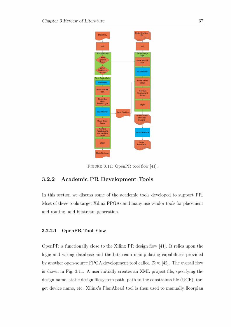
Chapter 3 Review of Literature 37
PartialyDesignBuild
StaticyDesignyBuild
Floorplanning
siteBlocker
PlaceywithyISEtools
RouteyBusMacro
Passthroughs
routeBlocker
RouteyStaticDesign
RemovePassthroughsandyblocking
routes
bitgen
PlaceywithyISEtools
routeBlocker
RouteyPartialDesign
bitgen
DefineDynamicRegion
SelectBusMacroLocations
StaticyBitstream
StaticyClocktree
StaticyHDLPartialyModules
HDL
PartialBitstreams
FullyBitstreamsforyPartialDesigns
partialGenerator
xst xst
RemoveConfinement
Routes
Figure 3.11: OpenPR tool flow [41].
3.2.2 Academic PR Development Tools
In this section we discuss some of the academic tools developed to support PR.
Most of these tools target Xilinx FPGAs and many use vendor tools for placement
and routing, and bitstream generation.
3.2.2.1 OpenPR Tool Flow
OpenPR is functionally close to the Xilinx PR design flow [41]. It relies upon the
logic and wiring database and the bitstream manipulating capabilities provided
by another open-source FPGA development tool called Torc [42]. The overall flow
is shown in Fig. 3.11. A user initially creates an XML project file, specifying the
design name, static design filesystem path, path to the constraints file (UCF), tar-
get device name, etc. Xilinx’s PlanAhead tool is then used to manually floorplan
Chapter 3 Review of Literature 38
the reconfigurable regions. The OpenPR tool then generates the static design by
generating placement constraints, generating blocker routes to prevent the static
region from using routing resources in the PR regions, and merging the blockers
with the static design. Later, the clock tree routing information from the static
design is inserted into the reconfigurable modules. This is done by manipulating
some of the intermediate files generated by the Xilinx implementation tools. Fi-
nally, the partial bitstreams are generated with the help of the Xilinx bitstream
generation tools.
The major attraction of OpenPR is its availability as an open source development
platform. It also enables independent implementation of the static and reconfig-
urable modules. In other words, any modification in the static region does not
necessitates reimplementation of all PR modules.
3.2.2.2 GoAhead Tool Flow
GoAhead [43] attempts to overcome some of the limitations of the Xilinx incre-
mental PR design flow. In the incremental flow, the static part of the system is
implemented first, and partial modules are implemented incrementally over the
static part. Hence, routing between the static logic and PR regions is fixed us-
ing bus macros, as discussed in Section 3.2.1.1. This means any modification in
the static logic requires complete re-implementation of all the PR modules. Since
static routes are allowed to pass through reconfigurable regions in the Xilinx flow,
module relocation between PR regions is also not feasible. GoAhead tries to over-
come these issues.
The overall GoAhead tool flow is shown in Fig. 3.12. The static and reconfigurable
modules are implemented through independent design flows. The designer makes
an initial plan defining the static parts of the design and modules which will be
reconfigured. Then, via a GUI, the design is floorplanned and bounding boxes are
drawn around PR regions. GoAhead then implements the static portion of the
design, while masking the PR regions with blocker macros that occupy all wires
inside the PR regions, thereby preventing static nets from crossing PR regions.
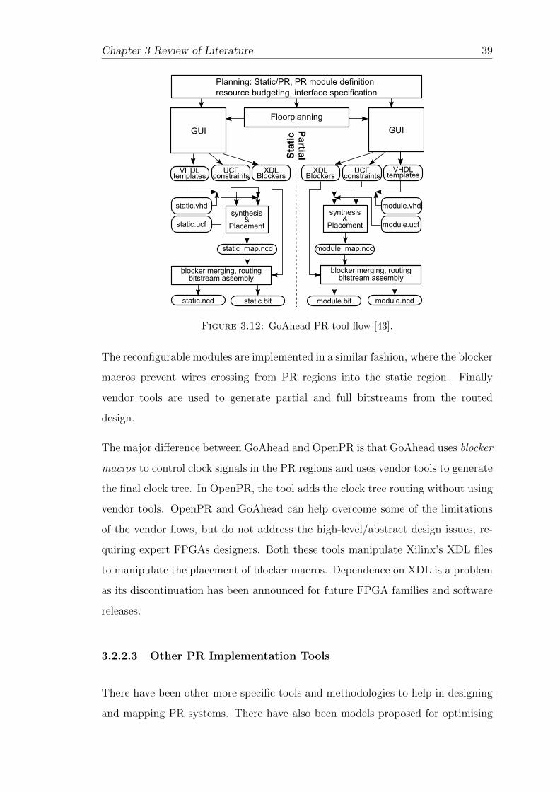
Chapter 3 Review of Literature 39
Planning:LStatic/PR,LPRLmoduleLdefinitionresourceLbudgeting,LinterfaceLspecification
Floorplanning
GUI GUI
VHDLtemplates
UCFconstraints
XDLBlockers
static.vhd
static.ucf
synthesisv
Placement
static_map.ncd
blockerLmerging,LroutingbitstreamLassembly
static.ncd static.bit module.bit module.ncd
blockerLmerging,LroutingbitstreamLassembly
module_map.ncd
module.vhd
module.ucf
synthesisv
Placement
VHDLtemplates
UCFconstraints
XDLBlockers
Static
Partial
Figure 3.12: GoAhead PR tool flow [43].
The reconfigurable modules are implemented in a similar fashion, where the blocker
macros prevent wires crossing from PR regions into the static region. Finally
vendor tools are used to generate partial and full bitstreams from the routed
design.
The major difference between GoAhead and OpenPR is that GoAhead uses blocker
macros to control clock signals in the PR regions and uses vendor tools to generate
the final clock tree. In OpenPR, the tool adds the clock tree routing without using
vendor tools. OpenPR and GoAhead can help overcome some of the limitations
of the vendor flows, but do not address the high-level/abstract design issues, re-
quiring expert FPGAs designers. Both these tools manipulate Xilinx’s XDL files
to manipulate the placement of blocker macros. Dependence on XDL is a problem
as its discontinuation has been announced for future FPGA families and software
releases.
3.2.2.3 Other PR Implementation Tools
There have been other more specific tools and methodologies to help in designing
and mapping PR systems. There have also been models proposed for optimising
Chapter 3 Review of Literature 40
PR systems [44, 45]. Many of these have not been publicly released, or rely on
hypothetical architectures, and hence they have not gained widespread adoption.
The Caronte methodology [46] takes a fixed task-graph as input and determines
how to allocate tasks to the regions specified by the designer in order to com-
plete execution of the application with dynamic loading of tasks. The designer is
assumed to have determined how many regions to use and to have floorplanned
them. Runtime management is done using an embedded processor.
A set of CAD tools for PR was developed by Robertson and Irvine [47]. These
tools include options for design specification, simulation (functional and timing),
synthesis, placement and routing, partial configuration generation and control of
partially reconfigurable designs. The tools, for simulation, placement and bit-
stream generation, target older generation FPGAs and none are publicly available
to the research community.
The GePaRD flow [48] tries to enhance the Xilinx PR flow with a high-level
synthesis framework. The flow uses a high-level specification of the PR system
as input and generates both a system model for simulation and a physically-
aware architecture description as input for implementation on the target device
using the Xilinx PR design flow. The design flow includes template abstraction,
high-level synthesis, and temporal modularisation. The authors do not specify
how the output of the proposed framework can be integrated with the vendor
toolflow to generate real systems. It targets a virtual architecture that adapts to
the reconfiguration mechanisms of a dedicated target device, but this mapping is
not explained.
An object-oriented framework for PR design and implementation was presented
by Abel [49]. It consists of a software-to-hardware compiler, an NoC with reliable
data buffering, a merger, and an adaptive scheduler and a Java emulator. Although
this framework provides some abstraction of runtime management for PR systems,
the hardware implementation is entirely based on the Xilinx toolflow, requiring
manual partitioning and floorplanning.
Chapter 3 Review of Literature 41
The design framework in [50] defines an adaptive system with two planes. The
data plane implements the data processing, such as the signal processing in a
radio, and can be composed using a high level tool that stitches together blocks
from an IP library. The control plane implements the management and control
functionalities in software. The control plane can reconfigure the data plane as
needed, from software code written by an adaptive system designer. This frame-
work only supports a single reconfigurable region and suffers from moderate data
throughput due to the low-bandwidth link between software and hardware.
Another layer-based architecture is presented by Tan and DeMara in [51]. The
hierarchical framework considers three aspects: autonomous operation, task-level
modularity, and runtime scenario support. The different layers are the logic layer,
the translation layer, and the reconfiguration layer. The logic layer supports gen-
eral user-level applications, carrying out hardware-independent logic control on the
tasks running on the FPGA. The translation layer translates logic descriptions for
the tasks into specific physical details as reconfiguration data (bitstreams). The
reconfiguration layer includes the hardware platform and the low-level commu-
nication APIs. The framework targets generic FPGA implementations without
detailing practical implementation on commercially available FPGAs.
Table 3.2 summarises the features supported by the different PR development and
implementation tools. In [49] and [48] PR systems are described in high-level pro-
gramming languages such as C. Here, tasks executed by the system are modelled
as C functions and the tools extract the task graph from the high-level language
description. Caronte [46] claims to support high-level system modelling and auto-
matic partitioning into software and hardware tasks, but the exact methods used
are not discussed in any detail.
None of the available methods take care of automatic partitioning of modules into
multiple PRRs, with reference to system configurations. Either the designer has to
manually determine the number of PRRs in the system and make the correspond-
ing module assignments or the tools require information regarding the number of
PRRs in the FPGA. For both Xilinx and Altera PR tools, manual floorplanning
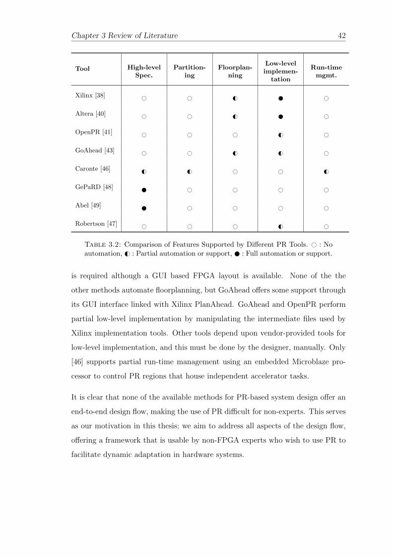
Chapter 3 Review of Literature 42
Tool High-levelSpec.
Partition-ing
Floorplan-ning
Low-levelimplemen-
tation
Run-timemgmt.
Xilinx [38] # # G# #
Altera [40] # # G# #
OpenPR [41] # # # G# #
GoAhead [43] # # G# G# #
Caronte [46] G# G# # # G#
GePaRD [48] # # # #
Abel [49] # # # #
Robertson [47] # # # G# #
Table 3.2: Comparison of Features Supported by Different PR Tools. # : Noautomation, G# : Partial automation or support, : Full automation or support.
is required although a GUI based FPGA layout is available. None of the the
other methods automate floorplanning, but GoAhead offers some support through
its GUI interface linked with Xilinx PlanAhead. GoAhead and OpenPR perform
partial low-level implementation by manipulating the intermediate files used by
Xilinx implementation tools. Other tools depend upon vendor-provided tools for
low-level implementation, and this must be done by the designer, manually. Only
[46] supports partial run-time management using an embedded Microblaze pro-
cessor to control PR regions that house independent accelerator tasks.
It is clear that none of the available methods for PR-based system design offer an
end-to-end design flow, making the use of PR difficult for non-experts. This serves
as our motivation in this thesis; we aim to address all aspects of the design flow,
offering a framework that is usable by non-FPGA experts who wish to use PR to
facilitate dynamic adaptation in hardware systems.

Chapter 3 Review of Literature 43
3.3 Low-Level PR Control Techniques
The limitations imposed by the vendor tool flow can significantly impact design
efficiency. For example, each generated bitstream is only suitable for a single
placement location on the FPGA: if a design requires a module to be placed in
different places at different times, multiple bitstreams are required for the same
module. Modules must also be implemented in a pre-defined region: if some modes
use less area, that is wasted while they are loaded. As a result of these issues,
much research has been undertaken to try and improve PR performance or reduce
some of the overheads associated with PR. However, many of these techniques
have become obsolete due to evolving FPGA architectures and a reduced amount
of detailed architecture information released by vendors.
3.3.1 Runtime Placement
While the vendor flows impose fixed regions within which modules are loaded, oth-
ers have explored how modules might be dynamically placed at runtime. Bazarghan
et al. considered this as an on-line bin-packing problem [52]. Later, Lu et al. intro-
duced an algorithm for online task placement [53]. Both these approaches assume
FPGAs to have a homogeneous architecture, allowing modules to be freely placed
in any location. Practically, FPGAs have heterogeneous architectures, especially
more recent devices, and connectivity between the modules must somehow be pre-
served while relocating them. Due to the complex routing architecture of FPGAs,
preserving routing is a very difficult problem to solve, which these approaches have
not addressed.
Another method for online placement and removal of modules on Virtex-II FPGAs
was presented in [54]. The approach performs the necessary routing to disconnect
and connect modules to others already present in the fabric. Before assigning a
new module to a region, the interface of the previous module is unrouted to prevent
any damage. However, this work only considered designs using CLBs exclusively.
Chapter 3 Review of Literature 44
Sandors et al. proposed a method to improve the placeability of modules with the
help of defragmentation [55]. Repeated placement and removal of modules without
placement constraints might cause free space to become fragmented, preventing
the allocation of new modules. A suitable defragmentation algorithm maximises
the continuous free-space available for module placement. Defragmentation was
also used in [56] to ease the relocation of modules. In [57], a method is proposed
for increasing the placeability of reconfigurable modules. The authors consider
regions consisting of reconfigurable tiles, supporting heterogeneous resources such
as BRAMs and DSP blocks. The algorithm defines the set of feasible positions
for PR modules and optimises the regions to minimise the degree of overlap with
other regions.
Another method for improving placeability is described in [58], targeting Virtex-4
FPGAs. The technique utilises a compatible subset of resources in non-identical
regions, making it possible to place modules in non-identical regions.
Several tools have been developed for online module placement targeting different
FPGAs. PARBIT (PARtial BItfile Transformer) was a widely used tool targeting
Virtex-E FPGAs [59]. Modules could be relocated by manipulating the contents
of a partial bitstreams. To generate a new placement, PARBIT reads the configu-
ration frames from the original bitstream and copies to the new partial bitstream
only the configuration bits related to the new area. It then generates new val-
ues for the configuration address registers. REPLICA (RElocation Per onLIne
Configuration Alteration) [60] was another tool targeting Virtex-E FPGAs. It is
implemented on the FPGA itself and performs address manipulation for reloca-
tion at run-time. Replica2Pro [61] was an advanced version supporting Virtex-II
and Virtex-II Pro FPGAs. It also supported relocation of BRAMs and multiplier
blocks.
The major disadvantage of online place-and-route tools is their lack of portability.
Due to architectural variations, the tools must be modified for each device, even for
different FPGAs in the same device family. The low-level details of configuration
frame contents available from Xilinx has also considerably decreased since the
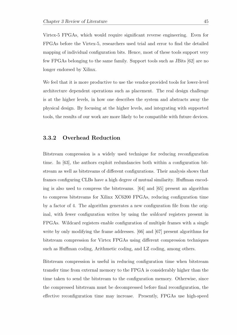
Chapter 3 Review of Literature 45
Virtex-5 FPGAs, which would require significant reverse engineering. Even for
FPGAs before the Virtex-5, researchers used trial and error to find the detailed
mapping of individual configuration bits. Hence, most of these tools support very
few FPGAs belonging to the same family. Support tools such as JBits [62] are no
longer endorsed by Xilinx.
We feel that it is more productive to use the vendor-provided tools for lower-level
architecture dependent operations such as placement. The real design challenge
is at the higher levels, in how one describes the system and abstracts away the
physical design. By focusing at the higher levels, and integrating with supported
tools, the results of our work are more likely to be compatible with future devices.
3.3.2 Overhead Reduction
Bitstream compression is a widely used technique for reducing reconfiguration
time. In [63], the authors exploit redundancies both within a configuration bit-
stream as well as bitstreams of different configurations. Their analysis shows that
frames configuring CLBs have a high degree of mutual similarity. Huffman encod-
ing is also used to compress the bitstreams. [64] and [65] present an algorithm
to compress bitstreams for Xilinx XC6200 FPGAs, reducing configuration time
by a factor of 4. The algorithm generates a new configuration file from the orig-
inal, with fewer configuration writes by using the wildcard registers present in
FPGAs. Wildcard registers enable configuration of multiple frames with a single
write by only modifying the frame addresses. [66] and [67] present algorithms for
bitstream compression for Virtex FPGAs using different compression techniques
such as Huffman coding, Arithmetic coding, and LZ coding, among others.
Bitstream compression is useful in reducing configuration time when bitstream
transfer time from external memory to the FPGA is considerably higher than the
time taken to send the bitstream to the configuration memory. Otherwise, since
the compressed bitstream must be decompressed before final reconfiguration, the
effective reconfiguration time may increase. Presently, FPGAs use high-speed
Chapter 3 Review of Literature 46
external memory devices such as DRAM for storing bitstreams, and the commu-
nication throughput supported is much higher than the maximum reconfiguration
throughput (400MB/s). Hence, bitstream compression has limited practical ap-
plication in reducing reconfiguration time. A better solution for this problem is
to increase the speed at which data is written to the configuration memory. It
is worth noting that FPGA vendors support custom bitstream compression tech-
niques, which does not require decompression before reconfiguration. For example,
Xilinx tools use a special register in the ICAP called multiple frame write register
(MFWR) to configure repeating frames in the bitstream to different configuration
memory locations. Thus frames which are repeating are removed from the bit-
stream with a special instruction to use MFWR to configure the corresponding
configuration memory locations.
Configuration caching is another method suggested for reducing reconfiguration
time. The technique described in [68] tries to minimise reconfiguration time in the
case of a task sequence that must executed in a fixed number of reconfigurable
regions. Simulated annealing is used to determine the allocation that minimises
reconfiguration time, leading to reductions by a factor of 5. For PR platforms exe-
cuting task level configurations, optimal scheduling algorithms are also developed
for minimising reconfiguration time [69, 70]. Such techniques only apply in the
case of using PR to switch tasks in a fixed-sequence implementation. For dynam-
ically adaptive systems, we do not know the transitions or specific order up front,
so such techniques cannot be applied. Optimisations at the allocation level must
be made taking into account information on valid transitions and, if available, the
frequency of those transitions.
3.4 Applications of Partial Reconfiguration
A number of applications have been developed which exploit the unique charac-
teristics of PR. Some applications fit the concept of partial reconfiguration very
well, while others benefit from improved efficiency through the use of PR.
Chapter 3 Review of Literature 47
3.4.1 Communication Systems
A popular application of PR is in software defined radio (SDR) [3], where com-
bining flexibility with hardware performance makes PR attractive. Frameworks
for building SDRs on PR-enabled FPGAs have already been proposed [2, 71, 72].
Cognitive radios are more advanced types of SDRs that modify their own func-
tionality at runtime in order to operate more efficiently in unknown environments.
Modifications of the modulation scheme, encoding format, and filters at runtime
necessitate low power hardware implementations that are also flexible. In exper-
imental work, radio designers will often use PCs to implement the radios, using
software running on GPPs, but for large deployments and experiments, a smaller
footprint can only be achieved with hardware implementation. In [71], the authors
suggest decomposing a cognitive radio into two parts: The Processor Subsystem
(PS) integrates the hardware modules required to run a standard Linux operating
system, while the Customisable Processing Subsystem (CPS), implements compo-
nents with high computational requirements. Flexible implementations of specific
radio blocks have also be demonstrated [72].
3.4.2 Multimedia
PR has also been used in audio and video processing applications. Processing cores
such as MP3 decoder [73], JPEG encoder [74] etc. are already implemented using
PR. For both implementations, the major motivation for using PR is to minimize
the total resource requirement as the logic availability in old generation FPGAs
were quite limited. It was demonstrated that operations such as JPEG encoding
can be temporally partitioned into smaller tasks, which can be sequentially config-
ured in the same PR region. In [75], a PR based scalable H.264/AVC deblocking
filter architecture is described. The filter adapts to different users’ requirements
intelligently. A real time video processing system using PR is described in [76].
Different types of image processing filters such as mean and median filters are
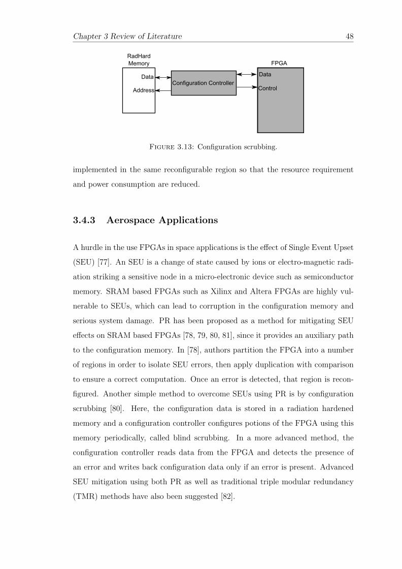
Chapter 3 Review of Literature 48
RadHardMemory
Configuration ControllerData
Address
Data
Control
FPGA
Figure 3.13: Configuration scrubbing.
implemented in the same reconfigurable region so that the resource requirement
and power consumption are reduced.
3.4.3 Aerospace Applications
A hurdle in the use FPGAs in space applications is the effect of Single Event Upset
(SEU) [77]. An SEU is a change of state caused by ions or electro-magnetic radi-
ation striking a sensitive node in a micro-electronic device such as semiconductor
memory. SRAM based FPGAs such as Xilinx and Altera FPGAs are highly vul-
nerable to SEUs, which can lead to corruption in the configuration memory and
serious system damage. PR has been proposed as a method for mitigating SEU
effects on SRAM based FPGAs [78, 79, 80, 81], since it provides an auxiliary path
to the configuration memory. In [78], authors partition the FPGA into a number
of regions in order to isolate SEU errors, then apply duplication with comparison
to ensure a correct computation. Once an error is detected, that region is recon-
figured. Another simple method to overcome SEUs using PR is by configuration
scrubbing [80]. Here, the configuration data is stored in a radiation hardened
memory and a configuration controller configures potions of the FPGA using this
memory periodically, called blind scrubbing. In a more advanced method, the
configuration controller reads data from the FPGA and detects the presence of
an error and writes back configuration data only if an error is present. Advanced
SEU mitigation using both PR as well as traditional triple modular redundancy
(TMR) methods have also been suggested [82].
Chapter 3 Review of Literature 49
3.4.4 Networking
PR also finds applications in networking. Within space applications, [83] describes
the implementation of the System-on-Chip Wire (SOCWire) architecture on a
partially reconfigurable Virtex-4 FPGA. SOCWire is a well established network-
on-Chip protocol in the space community, supporting link initialisation, credit-
based flow control, detection of link errors, link error recovery, hot-plug ability,
etc. The dynamic characteristic of this protocol makes it an ideal candidate for
PR based implementation.
A packet processing system called Field Programmable Port Extender (FPX) also
uses PR [84]. FPX contains logic to transmit and receive packets over a network
and dynamically reprogram hardware modules and route individual traffic flows.
The reconfigurable virtual network presented in [85] combines several partially-
reconfigurable hardware virtual routers with software virtual routers. Hardware
virtual routers are configured using dynamic reconfiguration. Functions such as
header verification, checksum verification, IP lookup, ARP lookup, and time to
live updates, etc., are implemented in PR regions. All these functions can be
implemented in a single region since they operate sequentially on a packet. The
forwarding table for the virtual router is also stored in PR regions and this can
be updated via a PCI bus using host software. This study shows that network
implementation based on PR gives better flexibility and forwarding performance
compared to a fixed hardware implementation.
In [86], the authors propose a method for power saving in networks by changing
the implementation of the same function under different conditions. By closely
monitoring the environmental changes and adapting the implementation according
to it, network power consumption can be reduced. The network environment
changes depending upon the number of users, time of day, distance from the
central node, etc. Power reduction not only reduces system running cost but also
improves reliability due to the lower thermal footprint.
Chapter 3 Review of Literature 50
3.4.5 Automotive Systems
Researchers have shown the potential of PR in automotive applications, especially
in driver assistance systems [87]. Since vehicles have a very long life, and fre-
quent upgrades are not possible, and given the rapid development of approaches
for driver assistance, PR on FPGAs offers the benefits of realtime video process-
ing with the flexibility to upgrade in future. In [1], the authors present a system
that uses a Power PC processor for control and management, with different im-
age processing functional units implemented as co-processors, loaded dynamically
as needed. Researchers have also proposed enabling redundancy in automotive
electronics through PR [88]. Here redundant electronic control units (ECUs) are
implemented in PR regions, and whenever an error condition is detected, the cor-
responding region is reconfigured to recover from the error, while a redundant
ECU with reduced performance acts as a backup.
3.4.6 Computational Science
PR has also been used extensively in high energy physics experiments. It was
used in the Compressed Baryonic Matter experiment conducted at the Facility for
Antiproton and Ion Research in Darmstadt, Germany [89]. This experiment used
an Active Buffer Board (ABB) for receiving, buffering and forwarding hit data. In
a high energy physics experiment, the surrounding conditions can change. Thus,
it was required that the ABB functionality change post-installation. PR was also
used in the ALICE (A Large Ion Collider Experiment) experiment conducted
in the CERN Large Hadron Collidor (LHC) [90]. Special photo-detectors were
used to monitor particles generated by the collisions in the LHC. A collection
of 120 Xilinx Virtex-4 FX FPGAs with PR were used for first level processing
and data reduction on the photo-detector outputs. PR is used to reconfigure
FPGA functionality without breaking the PCI Express communication with the
host server, which would happen in the case of a full reconfiguration.
Chapter 3 Review of Literature 51
3.4.7 Computing Systems
The dynamic instruction set computer (DISC) [91] supports demand-driven mod-
ification of its instruction set. Each instruction is implemented as an independent
circuit module, and these are paged into hardware in a demand-driven manner as
dictated by the application programme. Hardware limitations are eliminated by
replacing unused instruction modules with usable instructions at run-time. The
concept of high-performance reconfigurable computing has also been proposed [92].
Here, the FPGA takes on a significant portion of a large scientific application, with
PR allowing the fabric to be used by different computational steps at runtime.
In [93], autonomous computing systems were discussed, with placement and rout-
ing implemented on the FPGA fabric itself, allowing the FPGA to create new
bitstreams. The main challenge is the logic overhead of implementing these tools
and the slow speed of creating new bitstreams.
An emerging applications of PR is in accelerated cloud computing [94]. PR al-
lows integration of custom hardware accelerators that can be changed on demand.
While offering significant speedups in execution of a wide variety of tasks over
CPUs, FPGAs are also significantly more power-efficient, resulting in a compu-
tational efficiency improvement in the orders of magnitude over both CPUs and
GPUs [95, 96]. We expect work in this area to become much more prevalent in
the coming decade.
3.4.8 Machine Learning
PR has been successfully applied to pattern recognition and computer vision. [97]
presents an on-line evolvable pattern recognition system, where the classification
module is dynamically evolved using PR. Here a processor configures a PR region
with different classification modules to evaluate the input pattern. In [98], the Ad-
aBoost algorithm for human detection is implemented on a Virtex-4 FPGA using
PR. Two computationally intensive tasks, integral image computation and feature
Chapter 3 Review of Literature 52
extraction/decision, are alternately implemented in a single PR region. The out-
put of the first operation is used as the input for the second. The reconfigurable
implementation uses significantly fewer resources than a static (multiplexed) im-
plementation.
3.5 Summary
PR has evolved significantly over recent years, and found use in a diverse range of
applications. The design of PR systems remains hard, and hence, only accessible
to FPGA experts. Many published techniques for overcoming the limitations of
vendor tools are now defunct, as a result of the increasing heterogeneity of modern
devices, and less open access provided by vendors. Since many techniques are
also heavily tied to specific architectures, with their evolution, the tools become
unusable.
We believe the key implementation challenges are as a result of poor abstraction,
and a design flow that demands FPGA expertise. Hence, it is better to make
used of the vendor flow, but augment it with the required high-level design and
automation features, thereby opening up PR design to non experts, while also
ensuring some portability. When applying PR in the context of adaptive systems,
only limited information is available in advance, and this must be used to improve
mapping, while also maintaining the required flexibility. A flow that allows an
adaptive system designer to work at a modular level, without the need for deep
understand of the architecture or mechanisms of PR would open up the use of PR
in many new applications.
Chapter 4
Partitioning for Partial
Reconfiguration
4.1 Introduction
Determining the number of reconfigurable regions (PRRs) to use in a design and
how to allocate specific modules to them constitutes the design partitioning phase.
We saw in Chapter 2, that choices made during partitioning can significantly
impact both resource usage and reconfiguration time. In present PR design flows,
the designer must manually determine the number of PRRs and corresponding
module allocation to them and hence the granularity of reconfiguration.
The vendor tools require fixed regions to be determined before any partial bit-
streams can be generated, and those regions must abide by certain constraints.
These requirements are related to the way data is arranged in the configuration
memory, and must be met for the tools to generate valid partial bitstreams. Since
the tools will generate these partial bitstreams for a given netlist allocated to a
specific region, it is also the designer’s responsibility to determine that allocation.
Each region-module combination results in a new partial bitstream. As discussed
in Chapter 3, there have been some unofficial flows proposed that allow a single
bitstream to be modified to allow relocation. However, this is much more difficult
53
Chapter 4 Partitioning for Partial Reconfiguration 54
on new architectures with heterogenous resources, complex clock routing, and un-
released bitstream formats, and is also not supported by the vendor tools. The
communication interfaces between PRRs and between PRRs and the static region
are also fixed, and so, every module assigned to a specific PRR should follow the
corresponding interface standard.
Partitioning automatically, with consideration for these factors, can result in more
efficient implementations. Depending on the target application, the key metrics
for a design’s efficiency are resource utilisation and reconfiguration time. We have
already discussed how spatial multiplexing in a static design results in increased
area but a short reconfiguration time of just a few clock cycles. In a PR design,
reconfiguration takes time since a partial bitstream must be applied to the con-
figuration memory. Smaller regions can be reconfigured more quickly than larger
regions, since fewer frames make up the bitstream. However, they can adversely
impact area efficiency. Larger regions allow a design to use fewer resources, but
take longer to reconfigure, and must be configured more often (since any module
that is to be reconfigured affects the whole region). These are the two factors that
we take into account in optimising the partitioning step.
In this chapter, we present algorithms to automatically determine the optimal re-
gion allocation scheme for a given adaptive application. Based on a set of valid
system configurations, the method proposes the best arrangement of reconfigurable
regions and how modules should be assigned to them. For adaptive systems, recon-
figuration occurs on an as-needed basis, and is at the functional, rather than task
level. Functional level reconfiguration involves major modification to the datapath
such as a radio switching from sensing to transmission. Task level reconfiguration
refers to implementation of the different steps of a single computation as a sequence
of time-multiplexed hardware instances. Since adaptive systems apply functional
reconfiguration in response to changes in environmental conditions, we cannot pre-
dict the order and frequency of reconfiguration, so we must optimise globally to
reduce reconfiguration time and minimise area. All the implementations presented
in this Chapter are based on Xilinx PR toolflow.
Chapter 4 Partitioning for Partial Reconfiguration 55
The work presented in this chapter has also been discussed in:
• K. Vipin and S. A. Fahmy, Efficient Region Allocation for Adaptive Par-
tial Reconfiguration, in Proceedings of the International Conference on Field
Programmable Technology (FPT), New Delhi, 2011 [99].
• K. Vipin and S. A. Fahmy, Automated Partitioning for Partial Reconfig-
uration Design of Adaptive Systems, in Proceedings of the Reconfigurable
Architecture Workshop (RAW), Boston, USA, May 2013, pp. 172-181 [100].
4.2 Related Work
Much of the work on automated partitioning tries to schedule a graph of depen-
dent tasks onto a fixed number of regions, minimising runtime. They assume that
multiple FPGA regions are used similar to a multi-processor system with each
region processing an independent task. The work in [101] describes a reconfig-
urable processor system with two reconfigurable regions for execution speed up.
The speed up is achieved by overlapping the task execution in one region with the
reconfiguration of the other region. The task graph is partitioned in such a way
that reconfiguration and execution can be carried out concurrently without mutual
dependency. Similar work is presented in [102], in which a bitstream pre-fetching
schedule is generated based on control flow graphs, hence reducing the recon-
figuration time. For general adaptive systems, we do not have prior knowledge
of the sequence of configurations, so such methods cannot be applied. Instead,
we know what possible combinations of modules are required, and perhaps what
configuration transitions are possible, and must make decisions based on these.
In [103], the authors present a method for minimising reconfiguration latency based
on analysing communication graphs. The algorithm tries to group modules which
require simultaneous reconfiguration in the same reconfigurable region. However,
the number of reconfigurable regions must be determined by the designer. In [104],
the authors assume the number of reconfigurable regions is fixed and resources are
Chapter 4 Partitioning for Partial Reconfiguration 56
considered to be homogeneous. The number and size of the regions need to be
determined by the designer. Later, simulated annealing is used to assign hardware
modules to the regions by minimising the reconfiguration time. The number of
modules required to execute a task is assumed to be equal to the number of regions
and if any region is unoccupied, an empty module is assigned to it. Modern FPGAs
have a heterogeneous architecture with distributed DSP and BlockRAMs, which
defeats the homogeneous resource assumption.
The work in [105] explores partitioning and floorplanning in more detail. The
authors describe a simulated annealing based algorithm for determining the allo-
cation of modules to regions based on minimisation of area requirement variance
at different time instances. This work considers the latest FPGA architectures as
well as PR requirements. However, it also makes use of fixed task graphs for the
optimisation. Furthmore, the impact on reconfiguration time is not accounted for
in their method.
Most existing work does not perform partitioning in a manner that considers the
runtime aspects of PR and does not consider the latest FPGA architectures. They
generally assume a scheduled graph as the input where each task independently
executes in a region. For adaptive systems, we cannot rely on a fixed sequence of
configuration transitions, reconfiguration time can be critical to the application,
and we must also consider inter-region communication since modules work together
to implement a complete application.
4.3 Contributions
In this section we introduce algorithms for automating partitioning that consider
the detailed heterogeneous architecture of modern FPGAs, but in a manner that
is abstracted from the designer. We consider adaptive applications where reconfig-
uration occurs at the module level, and the sequence of configurations is unknown
up front. We focus on optimising reconfiguration time and resource usage. The
main contributions are:
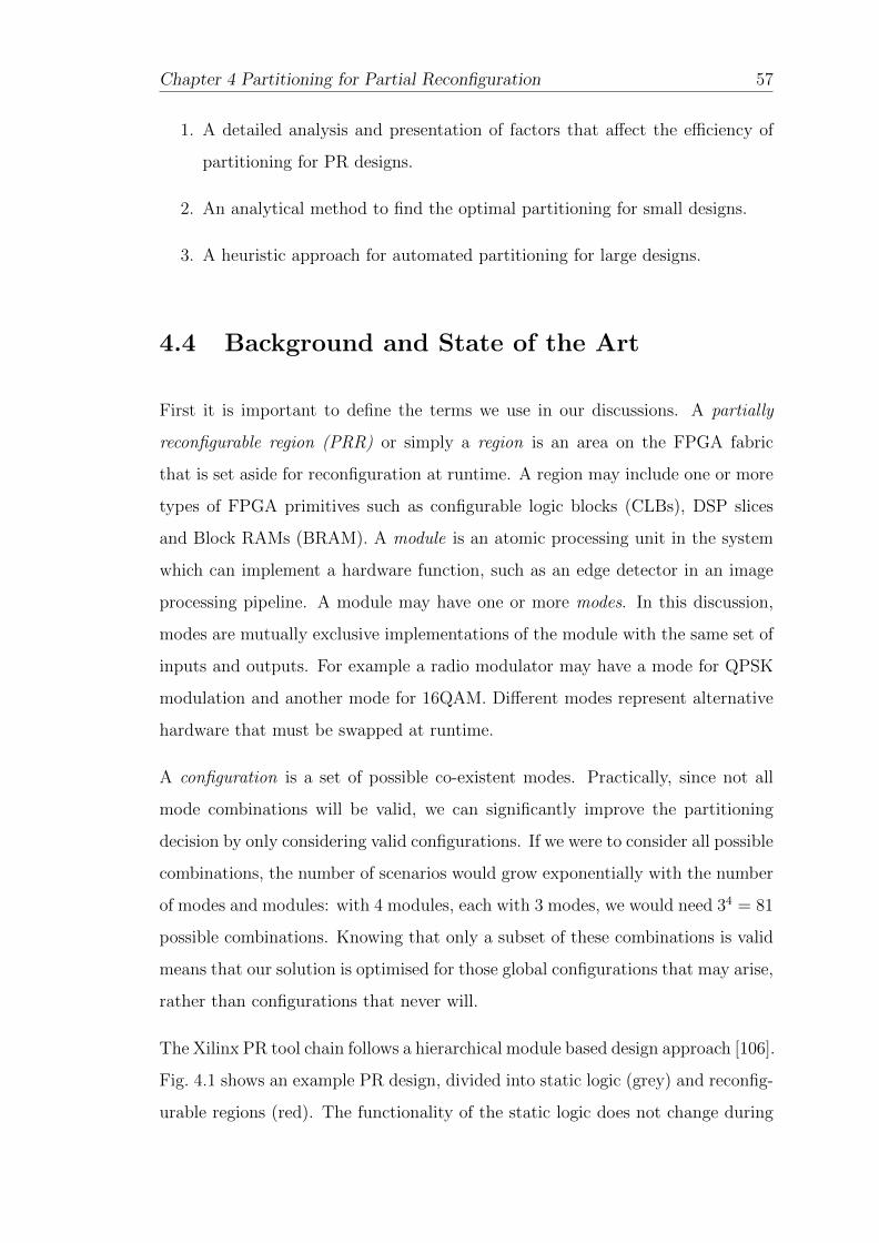
Chapter 4 Partitioning for Partial Reconfiguration 57
1. A detailed analysis and presentation of factors that affect the efficiency of
partitioning for PR designs.
2. An analytical method to find the optimal partitioning for small designs.
3. A heuristic approach for automated partitioning for large designs.
4.4 Background and State of the Art
First it is important to define the terms we use in our discussions. A partially
reconfigurable region (PRR) or simply a region is an area on the FPGA fabric
that is set aside for reconfiguration at runtime. A region may include one or more
types of FPGA primitives such as configurable logic blocks (CLBs), DSP slices
and Block RAMs (BRAM). A module is an atomic processing unit in the system
which can implement a hardware function, such as an edge detector in an image
processing pipeline. A module may have one or more modes. In this discussion,
modes are mutually exclusive implementations of the module with the same set of
inputs and outputs. For example a radio modulator may have a mode for QPSK
modulation and another mode for 16QAM. Different modes represent alternative
hardware that must be swapped at runtime.
A configuration is a set of possible co-existent modes. Practically, since not all
mode combinations will be valid, we can significantly improve the partitioning
decision by only considering valid configurations. If we were to consider all possible
combinations, the number of scenarios would grow exponentially with the number
of modes and modules: with 4 modules, each with 3 modes, we would need 34 = 81
possible combinations. Knowing that only a subset of these combinations is valid
means that our solution is optimised for those global configurations that may arise,
rather than configurations that never will.
The Xilinx PR tool chain follows a hierarchical module based design approach [106].
Fig. 4.1 shows an example PR design, divided into static logic (grey) and reconfig-
urable regions (red). The functionality of the static logic does not change during
Chapter 4 Partitioning for Partial Reconfiguration 58
A2A1
A3C2C1
C3B2B1
SPRR-1
PRR-2
PRR-3
Figure 4.1: Example PR design with 3 modules.
system operation—the static region is never reconfigured. There can be one or
more PRRs. In Fig. 4.1, S represents the static logic and there are three reconfig-
urable modules. A1, A2, and A3 are different modes of reconfigurable module A.
Reconfigurable modules must be implemented in PRRs, and a typical approach
is to allocate each module (and hence its modes) to a distinct region, thereby
allowing independent configuration of the modules. To do this, the designer must
allocate regions with sufficient resources to implement all modes of the module as-
signed to that region. This requires FPGA architecture knowledge and the regions
must also be manually floorplanned.
For the example design given in Fig. 4.1, S → A1 → B1 → C1 could be a possible
configuration. Each configuration contains the static logic and one of the possible
modes for each reconfigurable module. It is also possible that some configurations
do not contain any modes corresponding to one or more reconfigurable modules.
In the present PR tool flow, configurations do not play any role in synthesis since
the reconfigurable modules and the assignment of regions, are performed manually.
The designer prepares netlists only for valid combinations of module modes in each
region. Ideally, this process should be automated from a higher level description
of the valid configuration set.
Before discussing how to optimise partitioning and allocation, we should under-
stand the costs we are trying to minimise. The size of a partial bitstream is
proportional to the size of the region, and hence determines the reconfiguration
time. Whenever a module is reconfigured, the entire region to which it is assigned
must be reconfigured. Hence, while combining modules into fewer regions can al-
low the tools to optimize resource usage, it is clear that reconfiguration time can
increase dramatically. Furthermore, having more modules in a region means that
that region is likely to be configured more often. This work seeks to determine an
Chapter 4 Partitioning for Partial Reconfiguration 59
allocation that results in as small an area requirement as possible, and as short an
average reconfiguration time as possible.
4.5 Problem Formulation
4.5.1 Fundamentals
We formulate an analytical model that generates efficient PR allocations without
detailed inputs from the designer. Given an application description our method
defines the optimal number and size of PRRs and the assignment of modules to
those regions. This information can then be passed to the PR implementation
tools to generate the final partial bitstreams.
The easiest and the simplest way to partition for PR is to divide the whole FPGA
fabric into two: one static region and one PR region (PRR). All the static logic
in the design is implemented in the static region, while reconfigurable modules
are implemented in the PRR. This approach has two main benefits. Firstly, the
designer only needs to allocate a single region, large enough to hold the most
resource intensive configuration. Secondly, the implementation tools can optimise
resource usage and timing across all modules resulting in the best possible timing
performance since this method allows logic optimisation across module boundaries.
However, due to several drawbacks this method is not ideal. Firstly, whenever a
module in the region requires reconfiguration, the whole region has to be recon-
figured since partial bitstreams are generated on a region basis. Secondly, since
the whole region must be reconfigured even if a small module is being changed,
the reconfiguration time is increased, in some cases significantly. Finally, designs
with many possible combinations of modes will require a large bitstream for each
possible configuration, resulting in significant storage being required to store bit-
streams. This is again because the partial bitstreams are generated per region
and the size of the bitstreams is proporational to the size of the region. Thus
simply allocating all reconfigurable modules to a single region is not suitable for
Chapter 4 Partitioning for Partial Reconfiguration 60
systems that require minimised reconfiguration time or have limited bitstream
storage capacity.
Reconfiguration time can in some cases be the key requirement for an application.
Take for example a cognitive radio system that is reusing spectrum. If a primary
user appears, the radio must immediately cease sending and search for empty spec-
trum. Similarly, a driver assistance system should adjust between different scene
processing modes in as short a time as possible. Video applications may require
reconfiguration to take place in the inter-frame interval. Hence, it is important
to consider both worst-case and average reconfiguration times, as determined by
application constraints.
Generally, a one-region-per-module approach will offer the lowest worst-case re-
configuration times, since a region requires reconfiguration when its sole module
needs to be changed, and the size of the region is only as large as the largest mode
of that single module. However, a one-region-per-module approach is the least
area-efficient approach for region allocation since the total resource requirement is
the sum of the requirements of the largest mode of each module. The opportunity
for logic optimisation is also reduced since optimisation across region boundaries
is not possible.
System configurations play an important role in the following discussion. Config-
urations greatly reduce the search space, as we only need to consider allowable
mode combinations to arrive at an optimal allocation. By way of example, let us
represent configurations using an adjacency matrix. Each dimension represents
a module, with its corresponding modes. Each position in the matrix indicates
whether that combination of modes exists in any valid configuration. This is easy
to see for two modules. Consider module A, with modes A1 · · ·An and another
module B with modes B1 · · ·Bm. The adjacency matrix AA,B is an n×m matrix,
as shown.
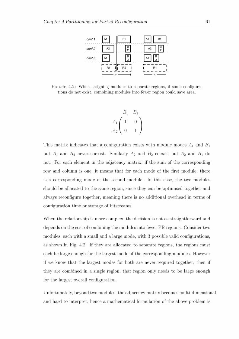
Chapter 4 Partitioning for Partial Reconfiguration 61
A1
A2
B1
B2
A1 B2
R1 R2
A1
A2
B1
B2
A1 B2
R1
> <
conf 1
conf 2
conf 3
Figure 4.2: When assigning modules to separate regions, if some configura-tions do not exist, combining modules into fewer region could save area.
B1 B2
A1 1 0
A2 0 1
This matrix indicates that a configuration exists with module modes A1 and B1
but A1 and B2 never coexist. Similarly A2 and B2 coexist but A2 and B1 do
not. For each element in the adjacency matrix, if the sum of the corresponding
row and column is one, it means that for each mode of the first module, there
is a corresponding mode of the second module. In this case, the two modules
should be allocated to the same region, since they can be optimised together and
always reconfigure together, meaning there is no additional overhead in terms of
configuration time or storage of bitstreams.
When the relationship is more complex, the decision is not as straightforward and
depends on the cost of combining the modules into fewer PR regions. Consider two
modules, each with a small and a large mode, with 3 possible valid configurations,
as shown in Fig. 4.2. If they are allocated to separate regions, the regions must
each be large enough for the largest mode of the corresponding modules. However
if we know that the largest modes for both are never required together, then if
they are combined in a single region, that region only needs to be large enough
for the largest overall configuration.
Unfortunately, beyond two modules, the adjacency matrix becomes multi-dimensional
and hard to interpret, hence a mathematical formulation of the above problem is

Chapter 4 Partitioning for Partial Reconfiguration 62
more appropriate, allowing multiple modules to be considered simultaneously, and
a globally optimal solution found.
4.5.2 Mathematical Formulation
To solve this problem analytically, we represent it mathematically using an objec-
tive function with a number of constraints. Based on the previous analysis, the
problem can be described as follows:
1. Minimise average reconfiguration time,
2. minimise total resource requirements.
Subject to the conditions:
1. The design fitting in the given device,
2. all modules in the design being implemented,
3. all required configurations being implemented,
4. each module being implemented only once,
5. the number of PR regions begin greater than or equal to 1 and less than or
equal to the total number of reconfigurable modules.
We assign the variables used in the formulation as shown in Table 4.1.
The maximum number of resource type i for module u is given by the maximum
usage of i among the different modes of u:
RuiMAX = maxm
(Rumi), (4.1)
Since each module is implemented only once, the sum of allocation decision vari-
ables should be 1: ∑q
duq = 1; ∀u (4.2)
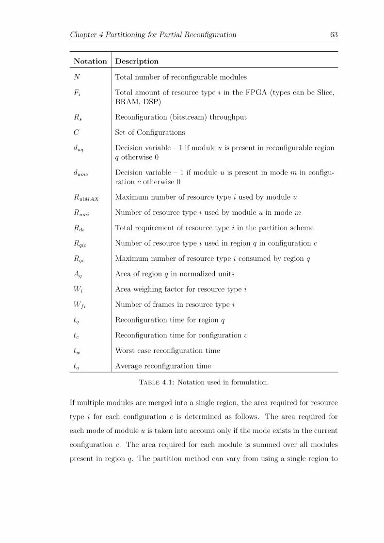
Chapter 4 Partitioning for Partial Reconfiguration 63
Notation Description
N Total number of reconfigurable modules
Fi Total amount of resource type i in the FPGA (types can be Slice,BRAM, DSP)
Rs Reconfiguration (bitstream) throughput
C Set of Configurations
duq Decision variable – 1 if module u is present in reconfigurable regionq otherwise 0
dumc Decision variable – 1 if module u is present in mode m in configu-ration c otherwise 0
RuiMAX Maximum number of resource type i used by module u
Rumi Number of resource type i used by module u in mode m
Rdi Total requirement of resource type i in the partition scheme
Rqic Number of resource type i used in region q in configuration c
Rqi Maximum number of resource type i consumed by region q
Aq Area of region q in normalized units
Wi Area weighing factor for resource type i
Wfi Number of frames in resource type i
tq Reconfiguration time for region q
tc Reconfiguration time for configuration c
tw Worst case reconfiguration time
ta Average reconfiguration time
Table 4.1: Notation used in formulation.
If multiple modules are merged into a single region, the area required for resource
type i for each configuration c is determined as follows. The area required for
each mode of module u is taken into account only if the mode exists in the current
configuration c. The area required for each module is summed over all modules
present in region q. The partition method can vary from using a single region to

Chapter 4 Partitioning for Partial Reconfiguration 64
using a separate region for each module.
Rqic =∑u
∑m
Rumi ∗ dumc ∗ duq; c = 1, 2, ...C (4.3)
For region q, from the set of resource requirements for different configurations,
the maximum resource requirement for type i is determined, which is the required
result.
Rqi = maxc
(Rqic) (4.4)
The total number of resources of type i required for the complete design is the
sum of resource type i required by all regions
Rdi =∑q
Rqi (4.5)
In order for the design to fit into a particular FPGA, for each resource type i, the
total resources required should be less than or equal to resource type i present in
the FPGA.
Fi −Rdi ≥ 0 (4.6)
The total area cost of region q is given by
Aq =∑i
Wi ∗Rqi (4.7)
where Wi is the weighing factor for resource type i, calculated as the ratio of total
resources to resources of type i.
Now consider reconfiguration time. Reconfiguration time for region q can be de-
termined by dividing the area of q by the reconfiguration throughput.
tq =∑i
Wfi ∗Rqi/Rs, (4.8)
where Wfi is the weighing factor determined by the number of reconfigurable
frames required for resource type i. This factor depends on the target FPGA
family as discussed in Section 3.1.2 and Table 3.1. When modules are merged,
Chapter 4 Partitioning for Partial Reconfiguration 65
reconfiguration of any of the modules in the region leads to reconfiguration of the
entire region. The frequency of reconfiguration depends on the application and
the system operating environment. Total configuration time for the system when
it changes from configuration ci to configuration cj is calculated as the sum of the
configuration times for regions, whose modules change their modes.
tc =∑q
tq ∗ dcq, (4.9)
where dcq = 1 if, for any duq = 1, dumci 6= dumcj else 0. Average reconfiguration
time is the average of all possible configuration times.
ta = t̄c (4.10)
Worst case reconfiguration time (tw) for a partition scheme is calculated as the
maximum reconfiguration time among all possible configuration transitions.
tw = max(tc) (4.11)
Depending on the requirement, the objective function can be selected as the total
area or reconfiguration time. In order to improve the overall system performance,
average reconfiguration time is selected as the minimisation objective in this case.
For applications where a strict reconfiguration time limit must be met, worst case
reconfiguration time can be used instead.
4.5.3 Integer Linear Programming
The exact solution for this problem can be found using Integer Linear Program-
ming (ILP). Although ILP is known to be NP-Complete, this formulation allows
us to find an optimal solution for smaller systems containing 10 or fewer reconfig-
urable modules which is common in practical use. In order to solve the problem
using an ILP solver, it is represented in a specific format having an objective
function and a number of constraints. From the above problem formulation, ILP

Chapter 4 Partitioning for Partial Reconfiguration 66
equations can be represented as
Minimise(∑q
Aq) (4.12)
or
Minimise(ta). (4.13)
subject to
∑q
duq = 1, (4.14a)
Aq =∑i
Wi ∗Rqi, (4.14b)
Rdi =∑q
Rqi, (4.14c)
Fi −Rdi ≥ 0, (4.14d)
tc =∑q
tq ∗ dcq, (4.14e)
ta = t̄c. (4.14f)
These equations can be solved by freely available ILP solvers such as LPSolve [107].
The solver is directed to sequentially increment the number of PRRs from 1 to
the number of reconfigurable modules. After each iteration, the best arrangement
for the present number of regions is compared with the previous best result and
the solution is updated. The solver can be also directed to find the pareto-optimal
points by including the second objective function (the one not used by the ILP
solver) in the comparison. The values ofWi, Wfi as well as the resource availability,
are FPGA-dependent. These are stored in a file and the solver is pointed to a
particular FPGA in order to find an optimal partitioning for that FPGA, or to
determine the most suitable FPGA device for the application.
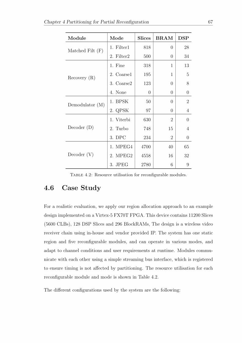
Chapter 4 Partitioning for Partial Reconfiguration 67
Module Mode Slices BRAM DSP
Matched Filt (F)1. Filter1 818 0 28
2. Filter2 500 0 34
Recovery (R)
1. Fine 318 1 13
2. Coarse1 195 1 5
3. Coarse2 123 0 8
4. None 0 0 0
Demodulator (M)1. BPSK 50 0 2
2. QPSK 97 0 4
Decoder (D)
1. Viterbi 630 2 0
2. Turbo 748 15 4
3. DPC 234 2 0
Decoder (V)
1. MPEG4 4700 40 65
2. MPEG2 4558 16 32
3. JPEG 2780 6 9
Table 4.2: Resource utilisation for reconfigurable modules.
4.6 Case Study
For a realistic evaluation, we apply our region allocation approach to an example
design implemented on a Virtex-5 FX70T FPGA. This device contains 11200 Slices
(5600 CLBs), 128 DSP Slices and 296 BlockRAMs, The design is a wireless video
receiver chain using in-house and vendor provided IP. The system has one static
region and five reconfigurable modules, and can operate in various modes, and
adapt to channel conditions and user requirements at runtime. Modules commu-
nicate with each other using a simple streaming bus interface, which is registered
to ensure timing is not affected by partitioning. The resource utilisation for each
reconfigurable module and mode is shown in Table 4.2.
The different configurations used by the system are the following:
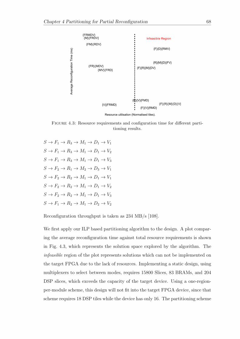
Chapter 4 Partitioning for Partial Reconfiguration 68
{FRMDV}{M}{FRDV}
{FR}{MDV}
{FM}{RDV}
{MV}{FRD}
{F}{D}{RMV}
{R}{V}{FMD}
{F}{R}{M}{DV}
{R}{M}{D}{FV}
{F}{R}{M}{D}{V}
Resource utilisation (Normalised tiles).
Ave
rage
Rec
onfig
urat
ion
Tim
e (m
s)
{F}{V}{RMD}
Infeasible Region
{V}{FRMD}
Figure 4.3: Resource requirements and configuration time for different parti-tioning results.
S → F1 → R3 →M1 → D1 → V1
S → F1 → R3 →M1 → D1 → V2
S → F1 → R3 →M1 → D1 → V3
S → F2 → R1 →M2 → D3 → V1
S → F2 → R2 →M1 → D1 → V1
S → F2 → R2 →M1 → D1 → V2
S → F2 → R2 →M1 → D1 → V3
S → F1 → R2 →M1 → D2 → V2
Reconfiguration throughput is taken as 234 MB/s [108].
We first apply our ILP based partitioning algorithm to the design. A plot compar-
ing the average reconfiguration time against total resource requirements is shown
in Fig. 4.3, which represents the solution space explored by the algorithm. The
infeasible region of the plot represents solutions which can not be implemented on
the target FPGA due to the lack of resources. Implementing a static design, using
multiplexers to select between modes, requires 15800 Slices, 83 BRAMs, and 204
DSP slices, which exceeds the capacity of the target device. Using a one-region-
per-module scheme, this design will not fit into the target FPGA device, since that
scheme requires 18 DSP tiles while the device has only 16. The partitioning scheme
Chapter 4 Partitioning for Partial Reconfiguration 69
in which all the modules are implemented in a single region (labelled {FRMDV})gives the lowest resource utilisation of 473 tiles, but the average reconfiguration
time for this scheme is considerably higher than other results, at 4.32 ms. Using
the proposed partitioning method, we can find schemes that fit the design into
the FX70T device with minimum reconfiguration time. The analytical method
enables us to choose one of the 6 Pareto optimal partitioning schemes depending
on application requirements.
The configuration in which the decoder (V) is implemented in a single region and
all other modules are implemented together in another region, labelled {V},{FRMD}in the plot, gives the lowest average reconfiguration time. This scheme uses 504
normalised tiles and has a average reconfiguration time of 2.52 ms. The scheme
in which the filter (F) and recovery (R) modules are combined in a single region
and other modules are implemented together (labelled {FR},{MDV} in the plot)
lies closest to the origin. This scheme uses 478 normalised tiles and the average
reconfiguration time is 3.54 ms and hence gives 13.5% area improvement compared
to one-module-per-region scheme. Worst case reconfiguration time for the optimal
scheme is 4.36 ms, while for the one-region-per-module, scheme, it is 4.69 ms.
The bitstream storage requirements for these schemes was also calculated. The
solution {FR},{MDV} requires 53 Mbits storage while implementing all modules
in a single region requires 81 Mbits to store bitstreams. These results depend
significantly on the configurations defined by the application. The upper bound
area consumption will be that of using separate regions for each module and the
lower bound is a single-region scheme.
One limitation of the proposed algorithm is its execution time as the design space
becomes larger. For the example case study, the solver was able to determine the
optimal solution in about 30 seconds. But as the number of modules increases,
the number of equations to be solved, and hence the solution space, also increases
exponentially. For example, a synthetic design with 10 modules, each with 10
modes, takes about 30 minutes to determine the final partition. To limit explo-
ration space, we have assumed that every mode belonging to the same module is
always implemented in the same region. This assumption may restrict the solver
Chapter 4 Partitioning for Partial Reconfiguration 70
from finding a more optimal solution as resource requirement variance between
modes belonging to different modules may be less than the variance among the
modes of same module. In the next section we discuss an improved heuristic
algorithm that removes this constraint.
4.7 An Improved Heuristic Partitioning Algo-
rithm
In this section, we introduce an improved partitioning algorithm that is more
flexible, and has improved runtime. Heuristics allow larger problems to be solved,
and by separating the logical association of modes of the same module, more
efficient allocations can be generated.
4.7.1 Partitioning Algorithm
The proposed algorithm tries to determine the best partitioning scheme for a
given PR system by minimising reconfiguration time. It can also be modified
to determine the partitioning resulting in the least resource consumption. The
algorithm can also suggest the smallest FPGA suitable to implement the given
design for non-time-critical applications.
The minimum possible area required for a PR system, excluding the static logic,
is the area of the largest configuration (when all the modes are implemented in
a single reconfigurable region). Hence, we first check implementation feasibility
by comparing this area with the resource availability of the selected FPGA. If the
resource availability is insufficient, the device choice is rejected and another device
must be chosen. If a solution is feasible, a connectivity matrix is generated with
each row representing a configuration and each column representing a reconfig-
urable module. This matrix is an M × N matrix, where each row represents a
configuration and each column represents a mode. Note that we remove the mod-
ule distinction in this formulation since that is only of relevance to the designer
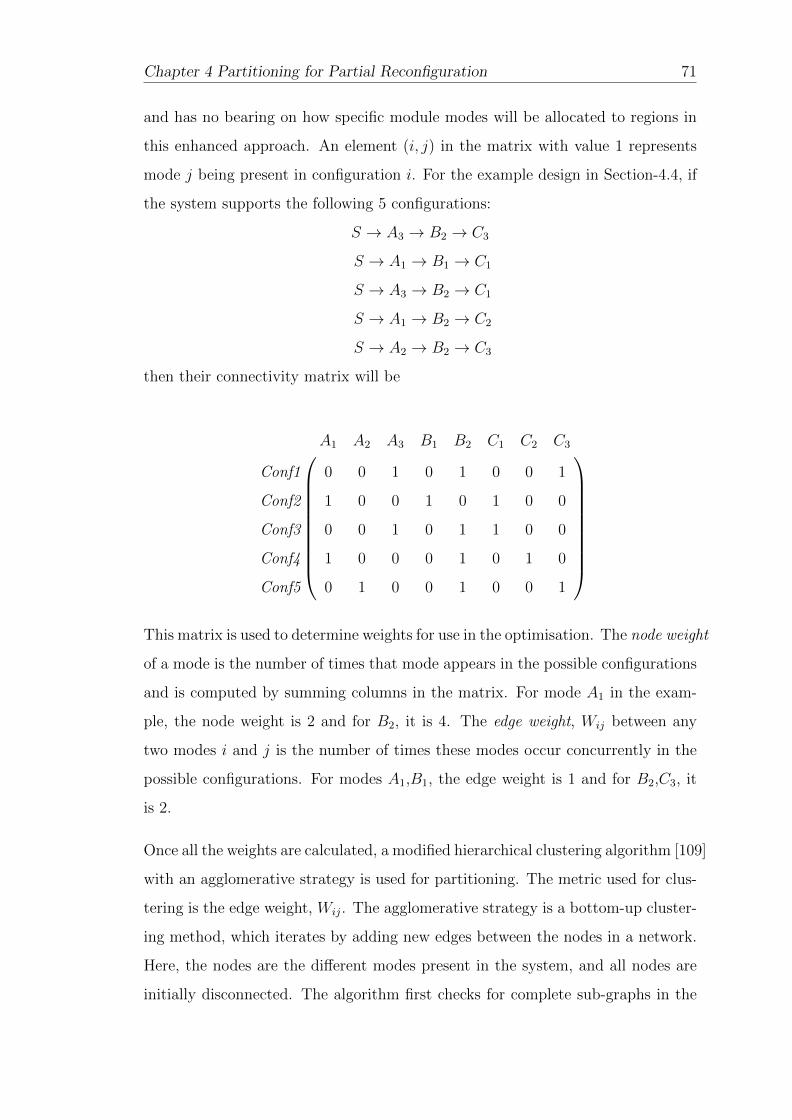
Chapter 4 Partitioning for Partial Reconfiguration 71
and has no bearing on how specific module modes will be allocated to regions in
this enhanced approach. An element (i, j) in the matrix with value 1 represents
mode j being present in configuration i. For the example design in Section-4.4, if
the system supports the following 5 configurations:
S → A3 → B2 → C3
S → A1 → B1 → C1
S → A3 → B2 → C1
S → A1 → B2 → C2
S → A2 → B2 → C3
then their connectivity matrix will be
A1 A2 A3 B1 B2 C1 C2 C3
Conf1 0 0 1 0 1 0 0 1
Conf2 1 0 0 1 0 1 0 0
Conf3 0 0 1 0 1 1 0 0
Conf4 1 0 0 0 1 0 1 0
Conf5 0 1 0 0 1 0 0 1
This matrix is used to determine weights for use in the optimisation. The node weight
of a mode is the number of times that mode appears in the possible configurations
and is computed by summing columns in the matrix. For mode A1 in the exam-
ple, the node weight is 2 and for B2, it is 4. The edge weight, Wij between any
two modes i and j is the number of times these modes occur concurrently in the
possible configurations. For modes A1,B1, the edge weight is 1 and for B2,C3, it
is 2.
Once all the weights are calculated, a modified hierarchical clustering algorithm [109]
with an agglomerative strategy is used for partitioning. The metric used for clus-
tering is the edge weight, Wij. The agglomerative strategy is a bottom-up cluster-
ing method, which iterates by adding new edges between the nodes in a network.
Here, the nodes are the different modes present in the system, and all nodes are
initially disconnected. The algorithm first checks for complete sub-graphs in the
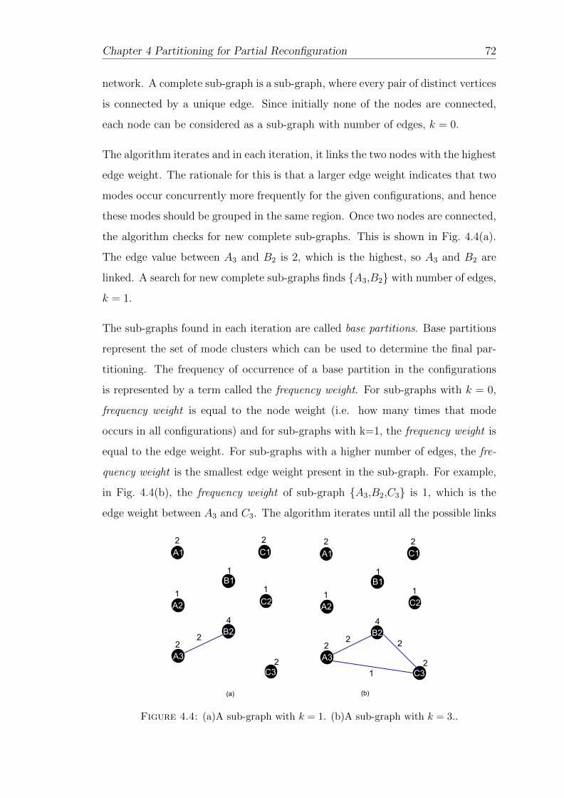
Chapter 4 Partitioning for Partial Reconfiguration 72
network. A complete sub-graph is a sub-graph, where every pair of distinct vertices
is connected by a unique edge. Since initially none of the nodes are connected,
each node can be considered as a sub-graph with number of edges, k = 0.
The algorithm iterates and in each iteration, it links the two nodes with the highest
edge weight. The rationale for this is that a larger edge weight indicates that two
modes occur concurrently more frequently for the given configurations, and hence
these modes should be grouped in the same region. Once two nodes are connected,
the algorithm checks for new complete sub-graphs. This is shown in Fig. 4.4(a).
The edge value between A3 and B2 is 2, which is the highest, so A3 and B2 are
linked. A search for new complete sub-graphs finds {A3,B2} with number of edges,
k = 1.
The sub-graphs found in each iteration are called base partitions. Base partitions
represent the set of mode clusters which can be used to determine the final par-
titioning. The frequency of occurrence of a base partition in the configurations
is represented by a term called the frequency weight. For sub-graphs with k = 0,
frequency weight is equal to the node weight (i.e. how many times that mode
occurs in all configurations) and for sub-graphs with k=1, the frequency weight is
equal to the edge weight. For sub-graphs with a higher number of edges, the fre-
quency weight is the smallest edge weight present in the sub-graph. For example,
in Fig. 4.4(b), the frequency weight of sub-graph {A3,B2,C3} is 1, which is the
edge weight between A3 and C3. The algorithm iterates until all the possible links
A1
A2
A3
B1
B2
C1
C2
C3
2
1
2
1
4
1
2
2
A1
A2
A3
B1
B2
C1
C2
C3
2
1
2
1
4
1
2
2
2 2 2
1
(a) (b)
Figure 4.4: (a)A sub-graph with k = 1. (b)A sub-graph with k = 3..

Chapter 4 Partitioning for Partial Reconfiguration 73
are added to the graph. The final sub-graphs detected are the full configurations,
with frequency weight 1. The resulting base partitions for the example design are
listed in Table 4.3.
Base Partition Freq. weight
{A2} 1
{C2} 1
{B1} 1
{A1} 2
{C1} 2
{C3} 2
{A3} 2
{B2} 4
{A1, B2} 1
{B2, C1} 1
{A1, C1} 1
{B2, C2} 1
{A2, B2} 1
Base Partition Freq. weight
{A1, C2} 1
{A1, B1} 1
{B1, C1} 1
{A2, C3} 1
{A3, C1} 1
{A3, C3} 1
{B2, C3} 2
{A3, B2} 2
{A3, B2, C3} 1
{A1, B1, C1} 1
{A3, B2, C1} 1
{A1, B2, C2} 1
{A2, B2, C3} 1
Table 4.3: Base partitions for example design their frequency weights.
Once base partitions are generated, a covering algorithm is used to select those
used for partitioning. For this purpose, the base partitions are arranged in a list
in ascending order of the number of modes included. As the number of modes in
a region increases, the frequency of reconfiguring that region increases, since mod-
ifying even a single mode in the region requires the complete reconfiguration of
the whole region. Since our objective is to minimise reconfiguration time, regions
are prioritised based on the number of modes. If two base partitions have the
same number of modes, they are arranged in ascending order of frequency weight.
Subsequent steps of the algorithm show that this prioritisation keeps the high fre-
quency base partitions as candidates when the algorithm iterates. Base partitions
with the same frequency weight are arranged in ascending order of their area.
Now base partitions are selected from the list in sequence order and compared
with the connectivity matrix. For each configuration (i.e. for each row in the
Chapter 4 Partitioning for Partial Reconfiguration 74
connectivity matrix) the corresponding modes present in the selected base partition
are set to zero. For example, the first base partition selected from the list is {A2}.For the fifth configuration, A2 is active. The corresponding element A2 is set to
zero and the fifth row of the connectivity matrix becomes
[0 0 0 0 1 0 0 1]
Subsequently, base partitions {C2}, {B1} etc. are used to cover more configu-
rations. Base partitions are selected and compared from the list until all ele-
ments in the matrix become zero. If a base partition does not cover any new
mode, it is not considered as a candidate. The set of base partitions used to
cover all configurations becomes a candidate partition set. In other words, a
candidate partition set is a set of base partitions, whose modes can cover all
the possible configurations. For the example design, the first candidate partition
set is {{A2}, {B1}, {C2}, {A1}, {C1}, {C3}, {A3}, and{B2}}. A closer examination
shows that these are actually all the modes present in the design.
As the next step, the tool finds the compatible set of partitions for each base
partition from the candidate partition set. Two partitions are compatible, if the
modes present in them do not co-occur in any of the configurations. For example
{A1} and {A2} are compatible partitions since they do not co-exist in any of the
possible configurations, while {A1} and {B1} are not compatible, since there is
a configuration S → A1 → B1 → C1. This step is necessary to make sure that
all configuration transitions are possible. If two base partitions required for a
single configuration are allocated to the same region, that configuration cannot be
implemented since at a given instance, only one base partition will be active in a
configurable region.
Region allocation starts by allocating each element of the candidate partition set
to a separate region, since this is equivalent to the static implementation which
requires minimum reconfiguration time. The total resource requirement and re-
configuration time for this partitioning is calculated. To find a new solution, two
compatible base partitions are assigned to the same region. The cost function for
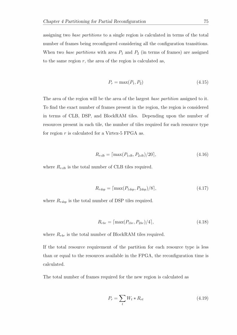
Chapter 4 Partitioning for Partial Reconfiguration 75
assigning two base partitions to a single region is calculated in terms of the total
number of frames being reconfigured considering all the configuration transitions.
When two base partitions with area P1 and P2 (in terms of frames) are assigned
to the same region r, the area of the region is calculated as,
Pr = max(P1, P2) (4.15)
The area of the region will be the area of the largest base partition assigned to it.
To find the exact number of frames present in the region, the region is considered
in terms of CLB, DSP, and BlockRAM tiles. Depending upon the number of
resources present in each tile, the number of tiles required for each resource type
for region r is calculated for a Virtex-5 FPGA as.
Rrclb = dmax(P1clb , P2clb)/20e, (4.16)
where Rrclb is the total number of CLB tiles required.
Rrdsp = dmax(P1dsp , P2dsp)/8e, (4.17)
where Rrdsp is the total number of DSP tiles required.
Rrbr = dmax(P1br , P2br)/4e, (4.18)
where Rrbr is the total number of BlockRAM tiles required.
If the total resource requirement of the partition for each resource type is less
than or equal to the resources available in the FPGA, the reconfiguration time is
calculated.
The total number of frames required for the new region is calculated as
Pr =∑t
Wt ∗Rrt (4.19)

Chapter 4 Partitioning for Partial Reconfiguration 76
Generatebase partitions
Select acandidate partition
Start
GenerateConnct. graph
Find compatiable partitions
Assign twopartitions
CalculateReconfig. time
All Compat.partitions checked?
No
Finish
New candidate partition
possible?
Yes
No
Yes
Figure 4.5: Flow chart for the proposed partitioning algorithm.
where t is the tile type, t ε (CLBs, DSP blocks, BlockRAMs),
Wclb = 36, Wdsp = 28 and Wbr = 30 for Virtex-5 family FPGAs
Wclb = 36, Wdsp = 28 and Wbr = 28 for Virtex-6 and 7-Series family FPGAs
System performance can be measured in terms of total reconfiguration time and
worst-case reconfiguration time. Total reconfiguration time gives a measure of
overall system performance, and is a useful proxy when we do not know the specific
configuration transitions up front, as is the case for adaptive systems. Total re-
configuration time is measured as the sum of all possible configuration transitions,
i.e. by considering transitions from all configurations to all other configurations.
If some statistical information about the probabilities of different configurations
occurring is known, this could be factored into the measure.
In some applications, such as real time systems and safety critical systems, the
system cannot tolerate reconfiguration time beyond a certain limit. Here it is
important that no configuration transitions take longer than this stipulated time.
Worst-case reconfiguration time is a useful measure in this situation. It is the
Chapter 4 Partitioning for Partial Reconfiguration 77
largest configuration transition time among all the possible configuration transi-
tions.
Mathematically, the total reconfiguration time is given by
ttotal =c−1∑i=1
c∑j=i+1
tconi,j j > i (4.20)
where, c is the total number of configurations, and tconi,j is the time required to
change the system configuration from i to j, and is calculated as
tconi,j =N∑r=1
di,j × tconr (4.21)
Where di,j is a decision variable which is equal to 1 if region r contains different
base partitions in configuration i and configuration j. tconr is the time to configure
region r and N is the total number of regions.
The configuration time for a region is proportional to the area of the region.
tconr ∝ Pr (4.22)
Hence total reconfiguration time in terms of frames is:
ttotal =c−1∑i=1
c∑j=i+1
N∑r=1
di,j ×∑t
Wt ∗Rrt (4.23)
t is the tile type, t ε (CLBs, DSP blocks, BlockRAMs),
The worst case reconfiguration time is calculated as
tworst = max(tconi,j) (4.24)
If the total reconfiguration time for the partition scheme is less than the present
lowest time, the scheme is stored as the present best partition scheme. Once
the total number of frames is calculated, base partitions assigned to the region
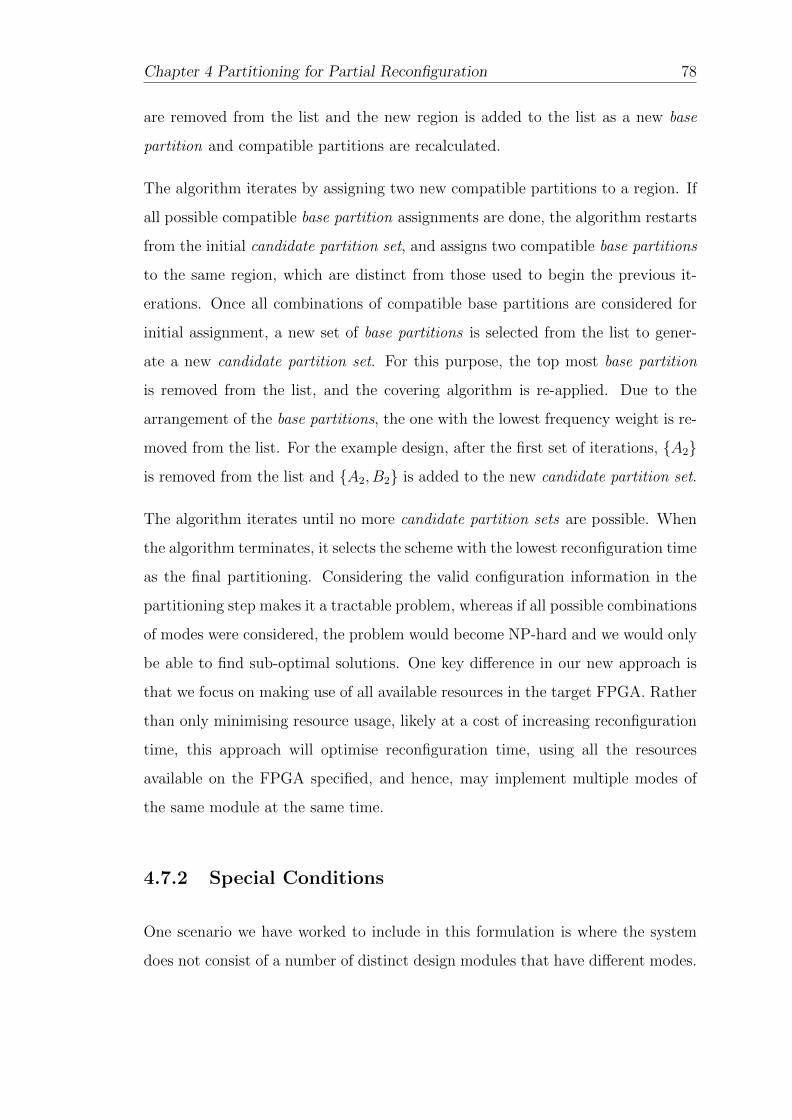
Chapter 4 Partitioning for Partial Reconfiguration 78
are removed from the list and the new region is added to the list as a new base
partition and compatible partitions are recalculated.
The algorithm iterates by assigning two new compatible partitions to a region. If
all possible compatible base partition assignments are done, the algorithm restarts
from the initial candidate partition set, and assigns two compatible base partitions
to the same region, which are distinct from those used to begin the previous it-
erations. Once all combinations of compatible base partitions are considered for
initial assignment, a new set of base partitions is selected from the list to gener-
ate a new candidate partition set. For this purpose, the top most base partition
is removed from the list, and the covering algorithm is re-applied. Due to the
arrangement of the base partitions, the one with the lowest frequency weight is re-
moved from the list. For the example design, after the first set of iterations, {A2}is removed from the list and {A2, B2} is added to the new candidate partition set.
The algorithm iterates until no more candidate partition sets are possible. When
the algorithm terminates, it selects the scheme with the lowest reconfiguration time
as the final partitioning. Considering the valid configuration information in the
partitioning step makes it a tractable problem, whereas if all possible combinations
of modes were considered, the problem would become NP-hard and we would only
be able to find sub-optimal solutions. One key difference in our new approach is
that we focus on making use of all available resources in the target FPGA. Rather
than only minimising resource usage, likely at a cost of increasing reconfiguration
time, this approach will optimise reconfiguration time, using all the resources
available on the FPGA specified, and hence, may implement multiple modes of
the same module at the same time.
4.7.2 Special Conditions
One scenario we have worked to include in this formulation is where the system
does not consist of a number of distinct design modules that have different modes.
Chapter 4 Partitioning for Partial Reconfiguration 79
For example consider the design example used in [105], that has only two config-
urations.
1. CAN controller (C) → FIR filter(F)
2. Ethernet controller (E) → Floating point unit (P) → CRC (R)
Here, there are no clear mode relations between the configurations. In our algo-
rithm this is dealt with by specifying each reconfigurable module as having just
a single mode. While specifying the configurations, the modules which are not
present in a configuration are marked as having mode 0. For this example, the
configurations are specified in our algorithm as
1. C1 → F1 → E0 → P0 → R0
2. E1 → P1 → R1 → C0 → F0
The algorithm treats mode 0 as the absence of the corresponding module, and no
column is allocated for zero modes in the connectivity matrix. This allows us to
mix multi-mode modules and one-off modules.
4.8 Case Study
Now we apply our heuristic approach to the same partitioning problem for the
wireless receiver described in Section 4.6. We use the same set of modules and con-
figurations targeting the Virtex-5 FX70T FPGA. The proposed algorithm finds a
solution that requires 6600 Slices, 60 BRAMs and 140 DSP blocks (536 normalised
tiles), with a total reconfiguration time of 235266 frames (164 ms at 234 MB/s
reconfiguration speed), 4% less than the one module per region implementation.
The low percentage improvement is due to the large size of the decoder module
modes compared to other modules and also since, in the final solution, all decoder
modes are assigned to the same region. The worst-case reconfiguration time for
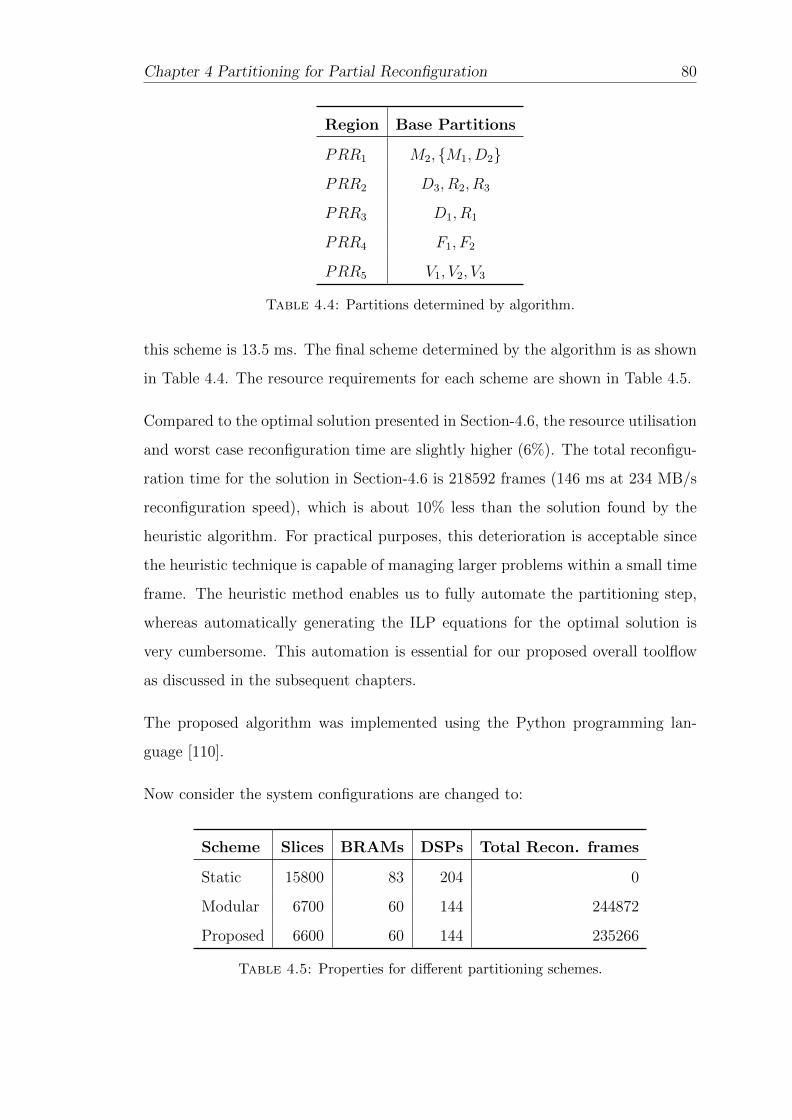
Chapter 4 Partitioning for Partial Reconfiguration 80
Region Base Partitions
PRR1 M2, {M1, D2}PRR2 D3, R2, R3
PRR3 D1, R1
PRR4 F1, F2
PRR5 V1, V2, V3
Table 4.4: Partitions determined by algorithm.
this scheme is 13.5 ms. The final scheme determined by the algorithm is as shown
in Table 4.4. The resource requirements for each scheme are shown in Table 4.5.
Compared to the optimal solution presented in Section-4.6, the resource utilisation
and worst case reconfiguration time are slightly higher (6%). The total reconfigu-
ration time for the solution in Section-4.6 is 218592 frames (146 ms at 234 MB/s
reconfiguration speed), which is about 10% less than the solution found by the
heuristic algorithm. For practical purposes, this deterioration is acceptable since
the heuristic technique is capable of managing larger problems within a small time
frame. The heuristic method enables us to fully automate the partitioning step,
whereas automatically generating the ILP equations for the optimal solution is
very cumbersome. This automation is essential for our proposed overall toolflow
as discussed in the subsequent chapters.
The proposed algorithm was implemented using the Python programming lan-
guage [110].
Now consider the system configurations are changed to:
Scheme Slices BRAMs DSPs Total Recon. frames
Static 15800 83 204 0
Modular 6700 60 144 244872
Proposed 6600 60 144 235266
Table 4.5: Properties for different partitioning schemes.
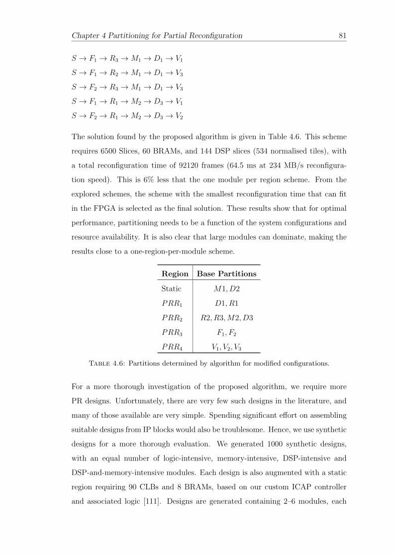
Chapter 4 Partitioning for Partial Reconfiguration 81
S → F1 → R3 →M1 → D1 → V1
S → F1 → R2 →M1 → D1 → V3
S → F2 → R3 →M1 → D1 → V3
S → F1 → R1 →M2 → D3 → V1
S → F2 → R1 →M2 → D3 → V2
The solution found by the proposed algorithm is given in Table 4.6. This scheme
requires 6500 Slices, 60 BRAMs, and 144 DSP slices (534 normalised tiles), with
a total reconfiguration time of 92120 frames (64.5 ms at 234 MB/s reconfigura-
tion speed). This is 6% less that the one module per region scheme. From the
explored schemes, the scheme with the smallest reconfiguration time that can fit
in the FPGA is selected as the final solution. These results show that for optimal
performance, partitioning needs to be a function of the system configurations and
resource availability. It is also clear that large modules can dominate, making the
results close to a one-region-per-module scheme.
Region Base Partitions
Static M1, D2
PRR1 D1, R1
PRR2 R2, R3,M2, D3
PRR3 F1, F2
PRR4 V1, V2, V3
Table 4.6: Partitions determined by algorithm for modified configurations.
For a more thorough investigation of the proposed algorithm, we require more
PR designs. Unfortunately, there are very few such designs in the literature, and
many of those available are very simple. Spending significant effort on assembling
suitable designs from IP blocks would also be troublesome. Hence, we use synthetic
designs for a more thorough evaluation. We generated 1000 synthetic designs,
with an equal number of logic-intensive, memory-intensive, DSP-intensive and
DSP-and-memory-intensive modules. Each design is also augmented with a static
region requiring 90 CLBs and 8 BRAMs, based on our custom ICAP controller
and associated logic [111]. Designs are generated containing 2–6 modules, each
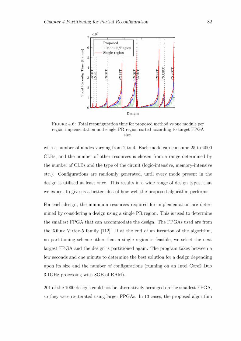
Chapter 4 Partitioning for Partial Reconfiguration 82
0
1
2
3
4
5
6
7·106
LX
20T
LX
30
FX
30T
SX
35T
FX
50T
SX
70T
FX
95T
FX
130T
FX
200T
Designs
Tota
lR
econ
fig
Tim
e(f
ram
es)
Proposed
1 Module/Region
Single region
Figure 4.6: Total reconfiguration time for proposed method vs one module perregion implementation and single PR region sorted according to target FPGA
size.
with a number of modes varying from 2 to 4. Each mode can consume 25 to 4000
CLBs, and the number of other resources is chosen from a range determined by
the number of CLBs and the type of the circuit (logic-intensive, memory-intensive
etc.). Configurations are randomly generated, until every mode present in the
design is utilised at least once. This results in a wide range of design types, that
we expect to give us a better idea of how well the proposed algorithm performs.
For each design, the minimum resources required for implementation are deter-
mined by considering a design using a single PR region. This is used to determine
the smallest FPGA that can accommodate the design. The FPGAs used are from
the Xilinx Virtex-5 family [112]. If at the end of an iteration of the algorithm,
no partitioning scheme other than a single region is feasible, we select the next
largest FPGA and the design is partitioned again. The program takes between a
few seconds and one minute to determine the best solution for a design depending
upon its size and the number of configurations (running on an Intel Core2 Duo
3.1GHz processing with 8GB of RAM).
201 of the 1000 designs could not be alternatively arranged on the smallest FPGA,
so they were re-iterated using larger FPGAs. In 13 cases, the proposed algorithm

Chapter 4 Partitioning for Partial Reconfiguration 83
0
1
2
3
4·104
LX
20T
LX
30
FX
30T
SX
35T
FX
50T
SX
70T
FX
95T
FX
130T
FX
200T
Designs
Wors
tR
econ
fig
Tim
e(f
ram
es)
Proposed
Single region
1 Module/Region
Figure 4.7: Worst case reconfiguration time for proposed method vs one mod-ule per region implementation and single PR region sorted sorted according to
target FPGA size.
was able to fit the design in a smaller FPGA than is required for the one module
per region scheme.
A comparison of total reconfiguration time for the one-module-per-region scheme,
a single-region scheme, and the scheme determined by the proposed algorithm
is shown in Fig. 4.6. The results have been sorted based on the target FPGA.
The total reconfiguration time for the single-region scheme is high since for each
reconfiguration, the complete PR region needs to be reconfigured. In most cases,
the proposed algorithm finds a better solution than the one-module-per-region
scheme.
A comparison for worst-case reconfiguration time is shown in Fig. 4.7. In al-
most all cases, the proposed algorithm has a lower worst-case reconfiguration time
compared to the one-module-per-region scheme. The plot shows that in several
scenarios, the worst-case reconfiguration time for a single-region scheme is lower
than the one-module-per-region scheme and the solution of the proposed algo-
rithm. This occurs because the single-region implementation scheme has the min-
imum resource requirement when all modes are implemented in PR regions (i.e.
no modes are moved to the static region). For this scheme, the worst-case recon-
figuration time is independent of configuration transitions, since each transition
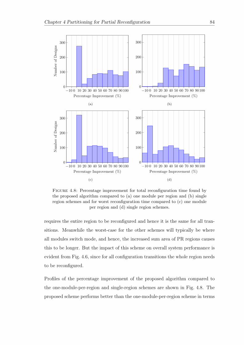
Chapter 4 Partitioning for Partial Reconfiguration 84
−10 0 10 20 30 40 50 60 70 80 901000
100
200
300
Percentage Improvement (%)
Number
ofDesigns
(a)
−10 0 10 20 30 40 50 60 70 80 901000
100
200
300
Percentage Improvement (%)
(b)
−10 0 10 20 30 40 50 60 70 80 901000
100
200
300
Percentage Improvement (%)
Number
ofDesigns
(c)
−10 0 10 20 30 40 50 60 70 80 901000
100
200
300
Percentage Improvement (%)
(d)
Figure 4.8: Percentage improvement for total reconfiguration time found bythe proposed algorithm compared to (a) one module per region and (b) singleregion schemes and for worst reconfiguration time compared to (c) one module
per region and (d) single region schemes.
requires the entire region to be reconfigured and hence it is the same for all tran-
sitions. Meanwhile the worst-case for the other schemes will typically be where
all modules switch mode, and hence, the increased sum area of PR regions causes
this to be longer. But the impact of this scheme on overall system performance is
evident from Fig. 4.6, since for all configuration transitions the whole region needs
to be reconfigured.
Profiles of the percentage improvement of the proposed algorithm compared to
the one-module-per-region and single-region schemes are shown in Fig. 4.8. The
proposed scheme performs better than the one-module-per-region scheme in terms
Chapter 4 Partitioning for Partial Reconfiguration 85
of total reconfiguration time in 73% of cases and performs better than the single-
region scheme in all cases.
In terms of worst-case reconfiguration time, the proposed algorithm finds a bet-
ter solution than the one-module-per-region scheme in 70% of cases. For 3 de-
signs, the output of the algorithm performs worse. Compared to the single-region
scheme, the proposed method improves or matches worst-case reconfiguration time
in 87.5% of cases. In the remaining 12.5% of cases, the total reconfiguration time,
which is what we optimise for, is very high and hence, this is not relevant.
We can see that the proposed algorithm offers tangible improvements over both
traditional partitioning approaches, especially in cases where it determines that
modules can be moved to the static region. At the same time, it is clear that using
general measures of total reconfiguration time and worst-case reconfiguration time
may not tell the whole story. A more detailed analysis would require knowledge of
the specific transition probabilities. By running the system for a period of time,
we could gain an understanding of which transitions are more likely and weigh
those more in the calculations.
4.9 Summary
Determining the number of partial reconfiguration regions and the allocation of
reconfigurable modules to regions is not always trivial, but this choice can impact
FPGA resource utilisation, reconfiguration time and the storage requirement for
configuration bitstreams. We have introduced a new technique, which can be
incorporated into the existing vendor-supported partial reconfiguration tool flow
to automate the partitioning step. We first presented an analytical formulation
that can determine an optimal mapping of modules to regions. We then presented a
more heuristic approach that treats each module mode independently, can allocate
some to the static region, and optimises for reconfiguration time. We demonstrated
that these approaches improve resource consumption and reduce reconfiguration
time for both real and synthetic adaptive applications. Automating partitioning

Chapter 4 Partitioning for Partial Reconfiguration 86
is the first step in a flow that allows a high level description to be mapped to a
fully functional PR implementation.
Chapter 5
Floorplanning PR Designs
5.1 Introduction
Floorplanning involves physical partitioning of the FPGA fabric for the optimal
placement of reconfigurable regions (PRRs) in order to improve routability, timing
or density. For standard non-PR based FPGA designs, floorplanning is generally of
less interest and is only used by expert designers to achieve high area optimisation
or timing performance. For static FPGA designs, the present vendor tools are
versatile enough to perform timing driven placement and routing, while fitting the
design within the available resources. Further manual tweaking can help improve
performance to meet particularly stringent time constraints.
Present vendor PR tools do not support automatic floorplanning, and require man-
ual inputs from the designer. To come up with an efficient floorplan, the designer
must have knowledge about the low-level physical architecture of the target FPGA,
as well as the run-time costs associated with PR. Manual floorplanning based on
these factors consumes a large amount of design time and is cumbersome, often
leading to sub-optimal results. This floorplanning requirement has contributed to
making PR less attractive to adaptive system designers, since most FPGA design-
ers never deal with floorplans for static designs. An intelligent arrangement and
allocation of PR regions can result in reduced area and hence allow designs to
87
Chapter 5 Floorplanning PR Designs 88
fit on smaller devices. It is also important to note that the implementation tools
cannot perform logic optimisation across the PRR boundaries, and hence, their
locations are important in achieving timing closure. We present a technique that
considers the runtime properties of PR to reduce reconfiguration time, by finding
a placement that factors in the lowest level granularity of heterogeneous resources
on modern FPGAs.
The work presented in this chapter has also been discussed in:
• K. Vipin and S. A. Fahmy, Architecture-Aware Reconfiguration-Centric Floor-
planning for Partial Reconfiguration, in Proceedings of International Sym-
posium on Applied Reconfigurable Computing (ARC), Hong Kong, 2012, pp.
13–25 [113].
5.2 Related Work
Although a number of approaches to FPGA floorplanning have been published,
work related to floorplanning for PR is less abundant. Traditionally, FPGA floor-
planning is considered as a fixed-outline floorplanning problem, as introduced
in [114] and further extended in [115]. The authors present a resource-aware
fixed-outline simulated-annealing and constrained floorplanning technique. Their
formulation can be applied to heterogeneous FPGAs but the resulting floorplan
may contain irregular shapes, which are not allowed in current PR flows. An-
other interesting study is presented in [116], which presents an algorithm called
“Less Flexible First (LFF)”. In order to perform placement, the authors define
the flexibility of the placement space as well as the modules to be placed. A cost
function is derived in terms of flexibility and a greedy algorithm is used to place
modules. The generated floorplan has only rectangular shapes, but the approach
only works with older-generation FPGAs and is unsuitable for recent families due
to their heterogeneous resource layout.
Chapter 5 Floorplanning PR Designs 89
The approach in [117] is based on slicing trees, and can ensure that the floorplan
contains only rectangular shapes. Here, the authors assume that the entire FPGA
fabric is composed of a repeating basic tile, which contains all types of FPGA
resources including Configurable Logic Blocks (CLBs), Block RAMs and DSP
slices. Although this assumption is valid for older-generation FPGAs, such as the
Xilinx Spartan-3, more recent FPGAs such as the Xilinx Virtex-6 family, do not
have such a repeated tile architecture.
Yuh et al. published two methods for performing floorplanning for PR. One
method is based on using a T-tree formulation [118] and the other is based on
a 3D-sub-Transitive Closure Graph (3D-subTCG) [119]. T-trees are tree based
data structures, which represent the spatial and temporal relations among tasks.
Using T-trees, each reconfigurable operation is represented as a 3D-box, with its
width and depth representing the physical dimensions and its height being the ex-
ecution time required for the operation. Here the reconfiguration operations are at
a task level rather than functional level and the authors consider older-generation
Virtex FPGAs, which require columnar reconfiguration.
In [105], the authors present a reconfiguration-aware “floorplacer”. Their algo-
rithm is based on the more recent Virtex-5 FPGA architecture. The algorithm
initially divides a design into reconfiguration regions based on the minimisation
of temporal variance of resource requirements. Then, the floorplacer tries to min-
imise area slack using simulated-annealing. In [120], a floorplanning method based
on sequence pairs is presented. In this work, the authors have shown how sequence
pairs can be used to represent multiple designs together. An objective function
tries to maximise the common areas between designs and simulated-annealing
is used for optimisation. Although simulated-annealing-based floorplanners have
been developed, for soft modules, which are common in PR designs, the results
are not satisfactory [121].
Since the work in this chapter was completed, a recent paper proposes the use of
mixed-integer linear programming to optimally solve the PR floorplanning prob-
lem [122] . Although this technique can provide improved results, a solution takes

Chapter 5 Floorplanning PR Designs 90
several hours for reasonably sized problems and the search space increases expo-
nentially with the number of regions. To reduce exploration time, they propose
that the designer provide an initial solution, which can then be refined using
heuristics. This, however, requires manual floorplanning on behalf of the designer
and the final result depends on this initial input.
Most existing work we have found focuses on the static properties of a particular
placement. Hence, the placement is not optimised for the dynamic behaviour of a
partially reconfigurable system. Other work relies on floorplanning for PR-based
region sharing of fixed task-graphs, only optimising for a fixed sequence of configu-
rations. We present an approach that optimises the runtime properties by finding
a placement that results in the lowest possible reconfiguration time, considering
the lowest level granularity of heterogeneous resources on modern FPGAs, for
designs where the adaptation is at a functional level and hence unpredictable.
5.3 Contributions
In this section we propose a novel algorithm, which can help system engineers
adopt PR without the need for manual floorplanning. Our floorplanner can be
integrated with our partitioning methods and the existing FPGA vendor tool
chain. In our method, we consider the runtime overheads associated with PR as
well as the characteristics of target FPGA devices. We are interested in recent
FPGA families such as the Xilinx Virtex-5, Virtex-6 and 7-series FPGAs, which
are highly heterogeneous in nature and have an irregular arrangement of Block
RAM and DSP columns. For PR applications, we are typically concerned with
reducing reconfiguration time and area. Cost functions are used that take into
account several factors such as resource wastage, wirelength and reconfiguration
time. The main contributions are:
1. A detailed analysis and presentation of factors that affect the efficiency of
floorplans for PR designs.
Chapter 5 Floorplanning PR Designs 91
2. A novel method for floorplanning on modern heterogeneous FPGA architec-
tures, that improves PR design characteristics.
3. A comparison of the proposed floorplanning efficiency with existing ap-
proaches.
5.4 PR Floorplanning Considerations
In order to unburden the designer from manual floorplanning, an automated PR
flow must take care of floorplanning. In this section, we develop a device model
and explore the factors to be considered in designing an efficient floorplanner for
PR. The limitations of several existing methods will be also explained.
Similar to the partitioning problem, it is possible to find an optimal floorplan
for a given set of PRRs and their connectivity using analytical methods. But the
equations required to solve the problem are complicated and require a large number
of variables to account for all the restrictions imposed by the implementation tools
and the architecture details of heterogeneous FPGAs. Different constraints would
be required for each different target device. The solution exploration space also
grows exponentially with the number of regions. Hence we adopt a heuristic
method which considers the architecture of heterogeneous FPGAs as well as the
restrictions imposed by PR implementation tools.
5.4.1 Architecture Considerations
For efficient floorplanning, the tool should be aware of the FPGA architecture and
special requirements arising due to PR. The details of the target Virtex FPGA
architecture have been discussed in Section 3.1.2. To summarise, columns of differ-
ent resource types are distributed horizontally, with the device an integer number
of rows high. One row by one column is a tile of a specific resource type, and
this is the finest granularity that can be reconfigured without extra complexity.
Chapter 5 Floorplanning PR Designs 92
Partial reconfiguration is performed by modifying the configuration memory por-
tions corresponding to the PR regions. Any modification to a region requires full
reconfiguration of the corresponding region. Reconfigurable regions should be con-
sidered in terms of tiles since configuration must occur on a per tile basis. To use
regions with incomplete tile boundaries, extra circuitry is required to read, mod-
ify, and write configuration information, resulting in increased area and latency.
Reconfigurable regions must always be rectangular in shape. Since each tile is
one device row high, the height of reconfigurable regions is an integer multiple of
device rows. The size of the bitstream, and hence the reconfiguration time of a
region, is directly proportional to the total area of the region, irrespective of how
many resources in the region are actually utilised.
In addition to other restrictions, 7-series FPGAs and hence Zynq SoCs have an
additional restriction of PRRs not dividing the interconnect tiles. In 7-series FP-
GAs, internal switch boxes control routing to two adjacent columns, and these
are interconnect tiles. Columns connected with the same switch boxes should be
within the same PRR. Due to this restriction the first CLB column of these devices
can not be included in a PRR since this column shares switch boxes with the I/O
column, and often, an additional CLB column is required in the PRR to avoid
intersecting the switch boxes.
5.4.2 Required Reconfigurable Area
A reconfigurable region implements different functional instances at various points
in time, and its area must be sufficient to accommodate the required configurations.
The required area (Ar), in frames, for a PR region is the net area required for
implementing all the module modes assigned to it. This area is calculated by
taking the maximal resource requirement for each resource type, considering the
tile thresholds. Multiplying this by the number of reconfiguration frames for each
tile type, gives an area measurement in terms of frames. Note that there is some

Chapter 5 Floorplanning PR Designs 93
overhead in this resource requirement due to it being based on whole tiles.
Ar =∑i
Wi ∗Ni, i ε CLB,DSP,BlockRAM. (5.1)
where Wj is the number of frames per type of tile i and Ni is the number of tiles
of type i needed.
5.4.3 Actual Reconfigurable Area
When a design is placed, the actual area may differ from the initial requirement due
to the rectangular shape requirement for PR regions or the disparate arrangement
of resources on the FPGA fabric. Mathematically, the actual area (Aa) of a region
is calculated as
Aa =∑i
Wi ∗Mi, i ε CLB,DSP,BlockRAM. (5.2)
where Wi is the number of frames per tile of type i and Mi is the number of tiles of
type i covered by the region. The result is the number of frames used to configure
the placed region.
5.4.4 Resource Wastage
The resource wastage for a particular placement of a reconfigurable region (Aw)
is the difference between the actual area and the required area of that region, in
frames. The total resource wastage of a full floorplan (Atw) is the sum of resource
wastage among all the regions.
Aw = Aa − Ar. (5.3)
Atw =∑r
Aw. (5.4)
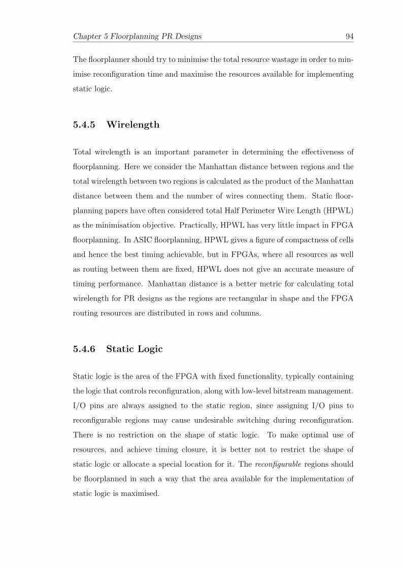
Chapter 5 Floorplanning PR Designs 94
The floorplanner should try to minimise the total resource wastage in order to min-
imise reconfiguration time and maximise the resources available for implementing
static logic.
5.4.5 Wirelength
Total wirelength is an important parameter in determining the effectiveness of
floorplanning. Here we consider the Manhattan distance between regions and the
total wirelength between two regions is calculated as the product of the Manhattan
distance between them and the number of wires connecting them. Static floor-
planning papers have often considered total Half Perimeter Wire Length (HPWL)
as the minimisation objective. Practically, HPWL has very little impact in FPGA
floorplanning. In ASIC floorplanning, HPWL gives a figure of compactness of cells
and hence the best timing achievable, but in FPGAs, where all resources as well
as routing between them are fixed, HPWL does not give an accurate measure of
timing performance. Manhattan distance is a better metric for calculating total
wirelength for PR designs as the regions are rectangular in shape and the FPGA
routing resources are distributed in rows and columns.
5.4.6 Static Logic
Static logic is the area of the FPGA with fixed functionality, typically containing
the logic that controls reconfiguration, along with low-level bitstream management.
I/O pins are always assigned to the static region, since assigning I/O pins to
reconfigurable regions may cause undesirable switching during reconfiguration.
There is no restriction on the shape of static logic. To make optimal use of
resources, and achieve timing closure, it is better not to restrict the shape of
static logic or allocate a special location for it. The reconfigurable regions should
be floorplanned in such a way that the area available for the implementation of
static logic is maximised.
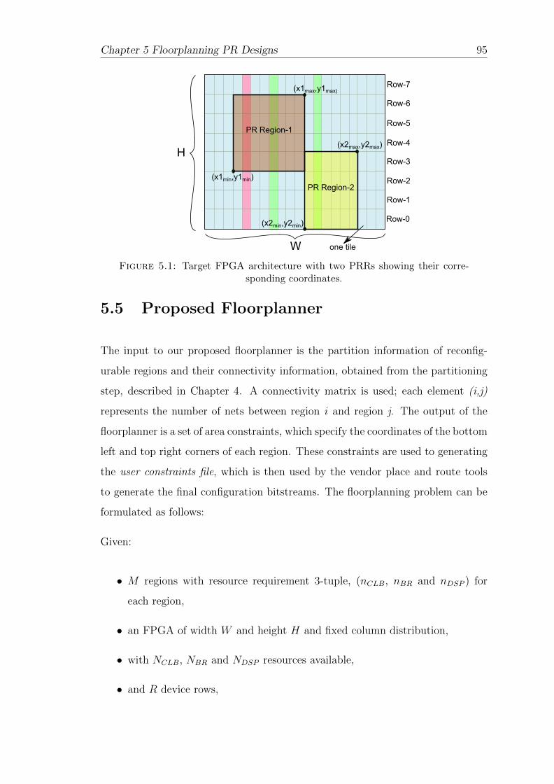
Chapter 5 Floorplanning PR Designs 95
PR Region-1
(x1min,y1min)
(x1max,y1max)
PR Region-2
(x2min,y2min)
(x2max,y2max)
Row-0
Row-1
Row-5
Row-4
Row-3
Row-2
Row-7
Row-6
H
W one tile
Figure 5.1: Target FPGA architecture with two PRRs showing their corre-sponding coordinates.
5.5 Proposed Floorplanner
The input to our proposed floorplanner is the partition information of reconfig-
urable regions and their connectivity information, obtained from the partitioning
step, described in Chapter 4. A connectivity matrix is used; each element (i,j)
represents the number of nets between region i and region j. The output of the
floorplanner is a set of area constraints, which specify the coordinates of the bottom
left and top right corners of each region. These constraints are used to generating
the user constraints file, which is then used by the vendor place and route tools
to generate the final configuration bitstreams. The floorplanning problem can be
formulated as follows:
Given:
• M regions with resource requirement 3-tuple, (nCLB, nBR and nDSP ) for
each region,
• an FPGA of width W and height H and fixed column distribution,
• with NCLB, NBR and NDSP resources available,
• and R device rows,
Chapter 5 Floorplanning PR Designs 96
BRAM Tile CLB Tile DSP Tile
(a)
(f)(e)(d)
(c)(b)
(g) (h)
Figure 5.2: Different kernels formed by the combinations of basic tiles.
partition the FPGA into M rectangles, so that:
• each region can be mapped into a rectangle, which contains sufficient re-
sources,
• each rectangle’s height is an integer multiple of device rows,
• no rectangles overlap,
• while minimising the cost function.
The outputs are the (xmin,ymin) and (xmax,ymax) coordinates of each rectangle so
that 0 ≤ xmin ≤ xmax ≤ W and 0 ≤ ymin ≤ ymax ≤ H as shown in Fig. 5.1.
5.5.1 Columnar Kernel Tessellation
Mapping an area directly using FPGA primitives is not practical, due to a number
of factors such as the large search space, limited number of available primitives
in the FPGA, fixed primitive locations and rectangular shape region constraint.
Hence we propose a new method called Columnar Kernel Tessellation. A kernel
is a structure one device row high, containing FPGA primitives, which can be re-
peated in the vertical direction to satisfy a region’s resource requirements. Fig. 5.2
shows a set of possible kernels for a Virtex FPGA. The availability of kernels for
floorplanning a region changes based on the floorplanning of previous regions. The
smallest kernel is a single tile. Each tile can be clustered with nearby tiles to form
new kernels.
Chapter 5 Floorplanning PR Designs 97
The first step of floorplanning is to calculate the resource usage of each region in
terms of reconfigurable tiles. For this purpose, the input resource utilisation values
are divided by the corresponding number of resources available in a tile. This may
result in some overhead if the resources needed do not use a whole number of
tiles. For example in Virtex-5 FPGAs, the required number of CLBs will be
divided by 20, DSPs by 8, and Block RAMs by 4 and in Virtex-6 FPGAs CLBs
by 40, and DSPs and Block RAMs by 8. Our floorplanner maintains a database
of FPGA architectures that contains information about the resource type of each
device column. The different types of columns are mapped to a single co-ordinate
system for better management. Each tile in the FPGA is encoded using a data-
structure with information including location, resource type, used or not, and
availability. Once a tile has been used to floorplan a region, its use field is set to
true. The tiles belonging to the locations of hard processors and transceivers are
set to be unavailable. To generate kernels, the resource column information from
the database is utilised. For each DSP column, the nearest Block RAM column
location is calculated. The nearest tiles of DSP and Block RAM along with the
tiles between them are merged to create kernels. These kernels are merged again
and larger kernels are created. When kernels are merged, the CLB tiles in between
them are also included in the resulting kernel. All kernels are one device row high.
Regions to be floorplanned are initially sorted in descending order based on re-
source requirements, to create a floorplanning schedule. The resource requirements
give a measure of fitting difficulty for each region; starting with the most resource-
intensive regions generally improves final results. Regions are selected based on
the following ordered criteria:
1. Require both DSP as well as Block RAM tiles,
2. Require DSP and CLB tiles,
3. Require Block RAM and CLB tiles,
4. Require CLBs tiles only.
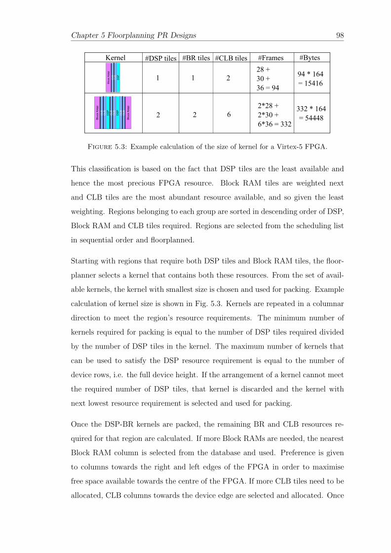
Chapter 5 Floorplanning PR Designs 98
Kernel #DSP*tiles #BR*tiles #CLB*tiles #Frames #Bytes
1 1 2
2 2 6
28*+*30*+*
*****36*=*94
2*28*+*2*30*+*
*******6*36*=*332
94***164=*15416
332***164=*54448
Blo
ck R
AM
CLB
CLB
DS
P
Blo
ck R
AM
DS
P
Blo
ck R
AM
DS
P
CLB
CLB
CLB
CLB
CLB
CLB
Figure 5.3: Example calculation of the size of kernel for a Virtex-5 FPGA.
This classification is based on the fact that DSP tiles are the least available and
hence the most precious FPGA resource. Block RAM tiles are weighted next
and CLB tiles are the most abundant resource available, and so given the least
weighting. Regions belonging to each group are sorted in descending order of DSP,
Block RAM and CLB tiles required. Regions are selected from the scheduling list
in sequential order and floorplanned.
Starting with regions that require both DSP tiles and Block RAM tiles, the floor-
planner selects a kernel that contains both these resources. From the set of avail-
able kernels, the kernel with smallest size is chosen and used for packing. Example
calculation of kernel size is shown in Fig. 5.3. Kernels are repeated in a columnar
direction to meet the region’s resource requirements. The minimum number of
kernels required for packing is equal to the number of DSP tiles required divided
by the number of DSP tiles in the kernel. The maximum number of kernels that
can be used to satisfy the DSP resource requirement is equal to the number of
device rows, i.e. the full device height. If the arrangement of a kernel cannot meet
the required number of DSP tiles, that kernel is discarded and the kernel with
next lowest resource requirement is selected and used for packing.
Once the DSP-BR kernels are packed, the remaining BR and CLB resources re-
quired for that region are calculated. If more Block RAMs are needed, the nearest
Block RAM column is selected from the database and used. Preference is given
to columns towards the right and left edges of the FPGA in order to maximise
free space available towards the centre of the FPGA. If more CLB tiles need to be
allocated, CLB columns towards the device edge are selected and allocated. Once
Chapter 5 Floorplanning PR Designs 99
the allocation is performed, the tiles which are used are marked in the database
as used.
Now the regions which use only DSP and CLB tiles are packed. For this pur-
pose, the kernels considered contain only DSP tiles and CLB tiles. The minimum
number of kernels required for packing will be equal to the number of DSP tiles
required divided by the number of DSP tiles in the kernel. Tiles which are not
marked as used or not available are used to generate the new set of kernels. This
same process is followed once more for regions containing Block RAMs. Finally,
regions containing only CLB tiles are planned.
The inherent rectangular shape of kernels and the columnar repetition guarantees
that the allocated area for each region will be of rectangular shape and region
height will be an integer multiple of device rows. The floorplanner follows a divide
and conquer method. The packing of each region reduces the search space for
implementing subsequent regions as well as the number of kernels available. The
algorithm runs a number of times, each time starting with a different kernel for
packing. The number of iterations can be specified or the search can be stopped
when a required cost objective is met. At the end of each complete packing, a cost
function is evaluated for the floorplan. The cost is defined as:
CF = α ∗ Atw + β ∗WL. (5.5)
where Atw is the total resource wastage and WL is the total wirelength between
regions. α and β are weight factors with α > β. For designs where reconfiguration
time is highly critical compared to speed of operation, the value of β can be set to
zero and for applications where system operating frequency (maximum operating
frequency) is critical rather than reconfiguration time α can be set to zero. For
other applications, the value of α and β are weighted accordingly.
At the end of each complete floorplan generation, a post processing step is per-
formed, in which the regions are moved along the columnar direction towards the
middle of the device. If this movement improves wirelength, the movement is ac-
cepted otherwise it is rejected. Also, regions that occupy the same columns are
Chapter 5 Floorplanning PR Designs 100
swapped and wirelength is recalculated. This move is also accepted only if it im-
proves wirelength. This is possible due to the fact that the resources are arranged
in columnar fashion in the FPGA, and moving a region along its columns does not
affect resource availability, provided there are no unavailable tiles in the direction
of movement.
5.6 Case Study
The proposed floorplanner was implemented in Python [110]. A direct comparison
of our method with existing methods is not possible due to the non-availability
of other floorplanning tools and uniform benchmark circuits. Hence, we use a
reported case study, taken from [105], and compared the results using our method.
The system implemented consists of a CAN controller, Floating Point Unit (FPU),
FIR filter, CRC controller and an Ethernet controller, housed in two reconfigurable
regions. The CAN controller, FPU and CRC are implemented in reconfigurable
region 1 (RR 1) and FIR filter and Ethernet controller are implemented in region
2 (RR2), as per [105]. The design is implemented on a Virtex-5 LX30T device.
Region 1 requires 24% of the available CLBs and 5 Block RAMs and region 2
requires 13% of the CLBs. The static region requires 61% of CLBs and 40 Block
RAMs. The resulting floorplan reported in the paper is shown in Fig. 5.4(a). It is
clear that although region 2 does not require Block RAMs or DSPs, the resulting
floorplan includes these resources. This leads to increased region size, higher
reconfiguration time and increased bitstream storage requirement. Furthermore,
these resources cannot be used elsewhere in the design. This floorplan uses a total
of 1766 frames.
A floorplan determined by our method is shown in Fig. 5.4(b). Region 2 is floor-
planned in such a way that no DSP slices and Block RAMs are used. Hence our
method uses 58 fewer frames and reserves more resources for static logic imple-
mentation. The smaller size of the region also contributes to 18.4 KB (9.2×2 since

Chapter 5 Floorplanning PR Designs 101
RR 1 RR 1
RR 2
RR 2
(a) (b)
Figure 5.4: (a) Resulting floorplan from [105], (b) Resulting floorplan fromour method.
there are two partial bitstreams for that region) less bitstream storage requirement
and a corresponding improvement in reconfiguration time.
For a more complex investigation, we could find no existing work to compare to,
nor standard tools to use, so we floorplanned an in-house design using our proposed
method and compared it to an ad-hoc floorplan based on previous experience with
some optimisation effort. The selected design is a software defined radio (SDR)
targeted for Xilinx Virtex-5 FX70T FPGA. The SDR chain consists of a matched
filter, carrier recovery, demodulator, signal decoder and video decoder. Each mod-
ule has a number of modes with different resource requirements. We assume each
module is assigned to a single region, and hence the resource requirements of each
region are the requirements of the largest mode of the module assigned to it. Here,
all modules are connected in sequential order with a 64 bit wide bus. The static
logic contains a PowerPC-440 embedded processor, external memory interface and
an ICAP controller. The different regions and associated resource requirements
are given in Table 5.1. The rq’d field indicates the exact number of resources
required, the tiles field indicates the required number of tiles needed to satisfy
the resource requirement and the waste field indicates the resources wasted due
to rounding the resources to tiles. The total number of frames wasted due to the
tiling operation is roughly 115 frames.
The ad-hoc floorplanning is done as per Xilinx PR floorplanning guidelines, with
the help of the PlanAhead software. Modules are selected one by one in the
order they appear in the processing chain and placed using the PlanAhead GUI.
Rectangular regions are chosen with the help of the software, which shows the
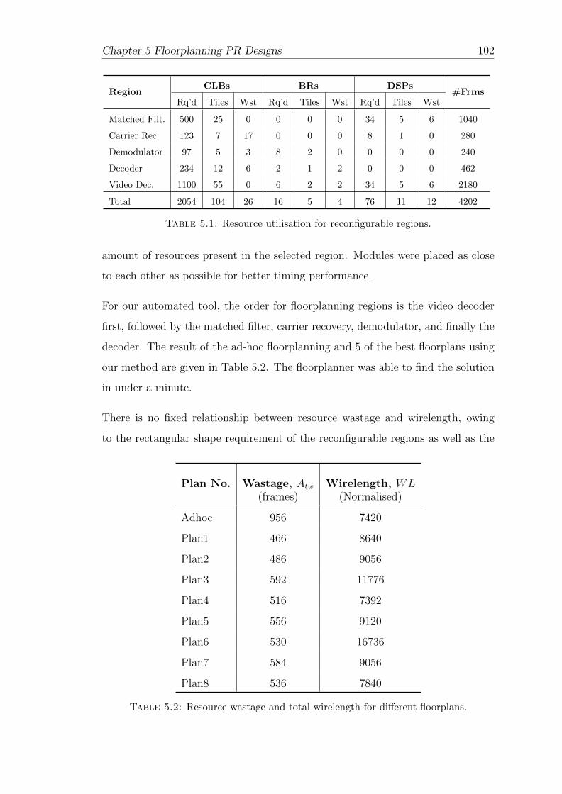
Chapter 5 Floorplanning PR Designs 102
RegionCLBs BRs DSPs
#FrmsRq’d Tiles Wst Rq’d Tiles Wst Rq’d Tiles Wst
Matched Filt. 500 25 0 0 0 0 34 5 6 1040
Carrier Rec. 123 7 17 0 0 0 8 1 0 280
Demodulator 97 5 3 8 2 0 0 0 0 240
Decoder 234 12 6 2 1 2 0 0 0 462
Video Dec. 1100 55 0 6 2 2 34 5 6 2180
Total 2054 104 26 16 5 4 76 11 12 4202
Table 5.1: Resource utilisation for reconfigurable regions.
amount of resources present in the selected region. Modules were placed as close
to each other as possible for better timing performance.
For our automated tool, the order for floorplanning regions is the video decoder
first, followed by the matched filter, carrier recovery, demodulator, and finally the
decoder. The result of the ad-hoc floorplanning and 5 of the best floorplans using
our method are given in Table 5.2. The floorplanner was able to find the solution
in under a minute.
There is no fixed relationship between resource wastage and wirelength, owing
to the rectangular shape requirement of the reconfigurable regions as well as the
Plan No. Wastage, Atw Wirelength, WL(frames) (Normalised)
Adhoc 956 7420
Plan1 466 8640
Plan2 486 9056
Plan3 592 11776
Plan4 516 7392
Plan5 556 9120
Plan6 530 16736
Plan7 584 9056
Plan8 536 7840
Table 5.2: Resource wastage and total wirelength for different floorplans.
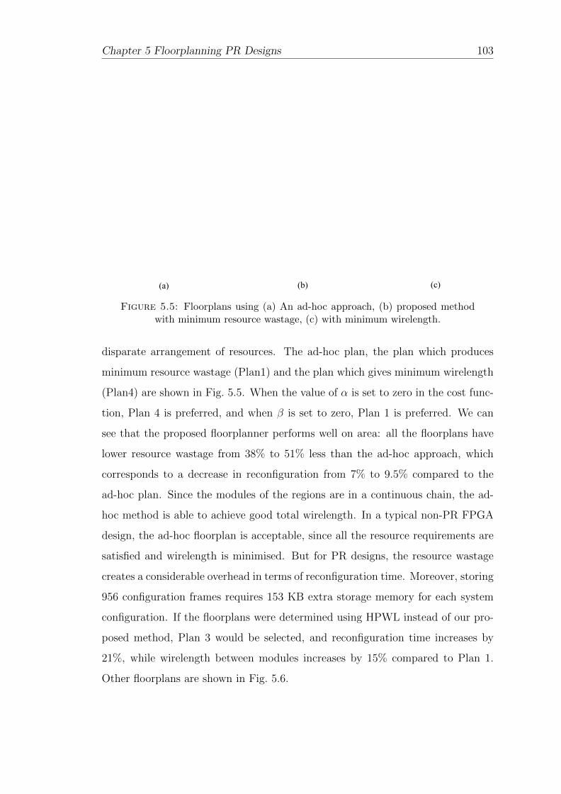
Chapter 5 Floorplanning PR Designs 103
(a) (b) (c)
Figure 5.5: Floorplans using (a) An ad-hoc approach, (b) proposed methodwith minimum resource wastage, (c) with minimum wirelength.
disparate arrangement of resources. The ad-hoc plan, the plan which produces
minimum resource wastage (Plan1) and the plan which gives minimum wirelength
(Plan4) are shown in Fig. 5.5. When the value of α is set to zero in the cost func-
tion, Plan 4 is preferred, and when β is set to zero, Plan 1 is preferred. We can
see that the proposed floorplanner performs well on area: all the floorplans have
lower resource wastage from 38% to 51% less than the ad-hoc approach, which
corresponds to a decrease in reconfiguration from 7% to 9.5% compared to the
ad-hoc plan. Since the modules of the regions are in a continuous chain, the ad-
hoc method is able to achieve good total wirelength. In a typical non-PR FPGA
design, the ad-hoc floorplan is acceptable, since all the resource requirements are
satisfied and wirelength is minimised. But for PR designs, the resource wastage
creates a considerable overhead in terms of reconfiguration time. Moreover, storing
956 configuration frames requires 153 KB extra storage memory for each system
configuration. If the floorplans were determined using HPWL instead of our pro-
posed method, Plan 3 would be selected, and reconfiguration time increases by
21%, while wirelength between modules increases by 15% compared to Plan 1.
Other floorplans are shown in Fig. 5.6.
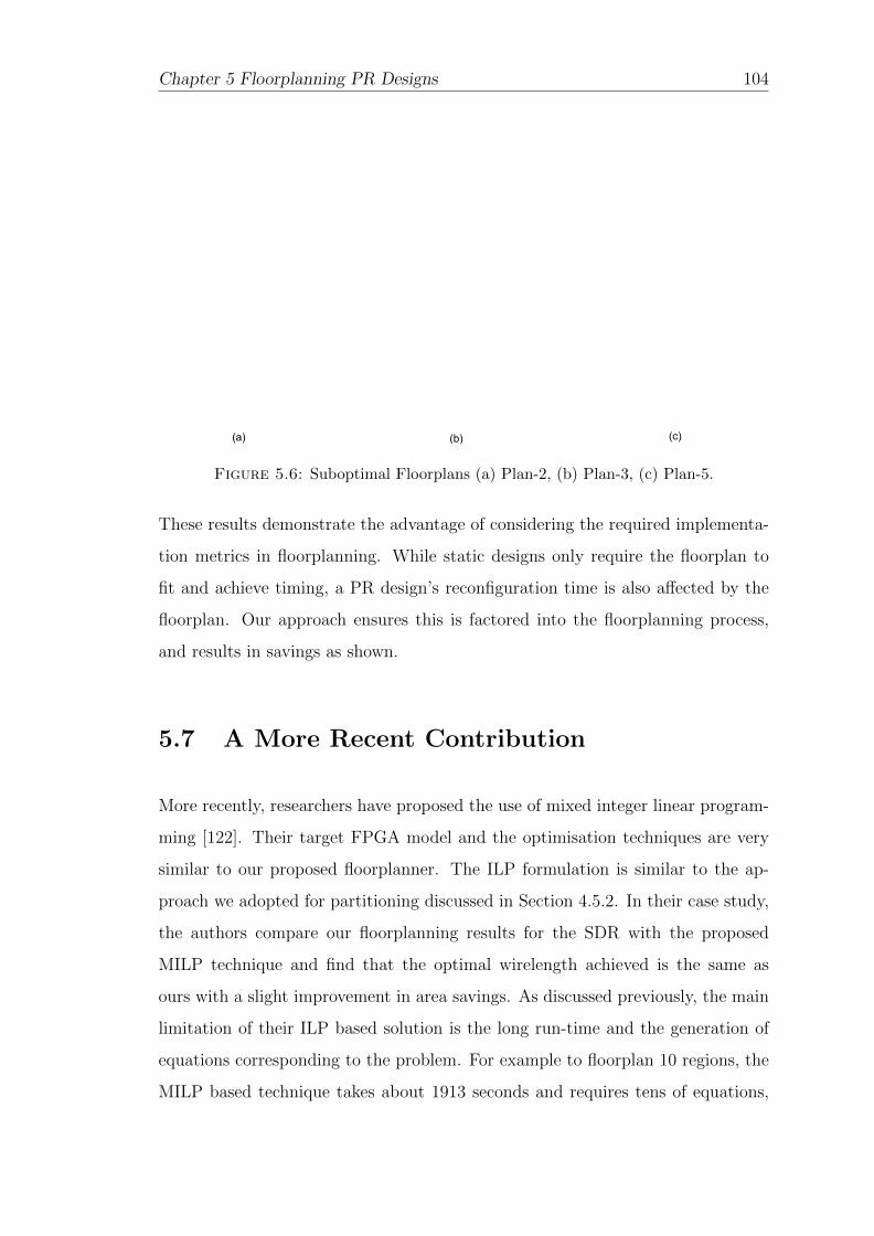
Chapter 5 Floorplanning PR Designs 104
(a) (b) (c)
Figure 5.6: Suboptimal Floorplans (a) Plan-2, (b) Plan-3, (c) Plan-5.
These results demonstrate the advantage of considering the required implementa-
tion metrics in floorplanning. While static designs only require the floorplan to
fit and achieve timing, a PR design’s reconfiguration time is also affected by the
floorplan. Our approach ensures this is factored into the floorplanning process,
and results in savings as shown.
5.7 A More Recent Contribution
More recently, researchers have proposed the use of mixed integer linear program-
ming [122]. Their target FPGA model and the optimisation techniques are very
similar to our proposed floorplanner. The ILP formulation is similar to the ap-
proach we adopted for partitioning discussed in Section 4.5.2. In their case study,
the authors compare our floorplanning results for the SDR with the proposed
MILP technique and find that the optimal wirelength achieved is the same as
ours with a slight improvement in area savings. As discussed previously, the main
limitation of their ILP based solution is the long run-time and the generation of
equations corresponding to the problem. For example to floorplan 10 regions, the
MILP based technique takes about 1913 seconds and requires tens of equations,
Chapter 5 Floorplanning PR Designs 105
which are specific to the problem. Our proposed heuristic technique is able to find
a solution in a few seconds without any manual intervention from the designer.
5.8 Summary
In this chapter we introduced a novel method for PR design floorplaning, that
is fully compatible with the recent vendor-supported PR tool-flows. The hetero-
geneous and irregular architecture of modern FPGA families is considered, and
floorplanning cost functions tailored for PR are introduced. It is worth noting
that this floorplanning method is also compatible with older generations of FP-
GAs such as Virtex-2, where frames extended the whole height of the device,
instead of a single device row. Our study proves that it is possible to optimise the
area requirement considering the tile constraint. We have also found that a signif-
icant area overhead can result from the tiling and rectangular area requirements
of reconfigurable regions. Hence, considering tiling at the partitioning stage, prior
to floorplanning may yield more efficient designs.

Chapter 6
Reconfiguration Controllers for
Adaptive Systems
6.1 Introduction
In Chapters 4 and 5 we discussed design-time optimisations to reduce resource util-
isation and reconfiguration time for PR-based adaptive systems. Run-time man-
agement, involving both the low-level hardware-dependent reconfiguration control
and the high-level software-based reconfiguration management, also plays an im-
portant role in overall system performance. For an adaptive system, reconfigura-
tion time is the time taken to switch from one configuration to another. For a
PR-based implementation, this corresponds to reconfiguring one or more regions
with specific partial bitstreams. During this time, for a dataflow system, it cannot
process data or may need to buffer it. Hence, reconfiguration time must be min-
imised. As discussed in Chapter 2, PR does entail a longer reconfiguration time
than simply spatially multiplexing modules, since a bitstream must be loaded.
For a PR-based system, reconfiguration control and reconfiguration management
can be tightly or loosely coupled. In a tightly-coupled architecture, both reconfigu-
ration control and management are implemented on the same physical FPGA and
in a loosely-coupled architecture, the reconfiguration management is implemented
106
Chapter 6 Reconfiguration Controllers for Adaptive Systems 107
externally. For a tightly-coupled architecture, either an embedded processor in
the FPGA (such as the ARM processor in the Zynq) or a soft-processor (such
as the Microblaze) can be used to manage reconfiguration. For a loosely-coupled
architecture, an external processor interfaced with the FPGA, directly or through
standard communication interfaces such as UART or PCIe, manages reconfigura-
tion.
Vendor-provided reconfiguration controllers give very low reconfiguration speed al-
though the physical reconfiguration interface is capable of achieving much higher
performance. When software based reconfiguration management is implemented,
vendor-supported approaches burden processors with managing low-level reconfig-
uration operations, adversely affecting reconfiguration time, and possibly making
it hard to use the processor for any other task. Much published work assumes a
dedicated processor for managing the PR process. However, considering proces-
sors are now an important part of many hardware systems, and the emergence of
architectures like the Xilinx Zynq, managing PR is now just one of the embed-
ded processor’s many tasks, and hence this must be considered carefully to ensure
reconfiguration does not impact other important tasks.
In this chapter, we discuss the design of low-level reconfiguration controllers for
PR based adaptive systems. We aim to maximise reconfiguration throughput,
thus minimising reconfiguration time. At the same time, these controllers provide
the necessary infrastructure to enable high-level reconfiguration management, as
discussed in Chapter 7. Existing published work uses ad-hoc software that ref-
erences bitstreams and memory locations explicitly to control PR. We decouple
hardware-dependent reconfiguration functions from overall adaptation manage-
ment, allowing design to be easier for non-experts and system implementation to
be more portable.
The work presented in this chapter has also been discussed in:
• K. Vipin and S. A. Fahmy, A High Speed Open Source Controller for FPGA
Partial Reconfiguration, in Proceedings of the International Conference on
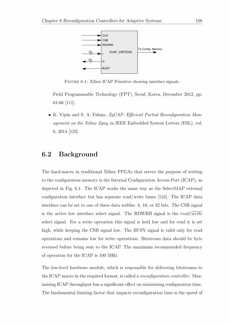
Chapter 6 Reconfiguration Controllers for Adaptive Systems 108
CLK
CSB
RDWRB
32I
32O
BUSY
ICAP_VIRTEX6To Config. Memory
Figure 6.1: Xilinx ICAP Primitive showing interface signals.
Field Programmable Technology (FPT), Seoul, Korea, December 2012, pp.
61-66 [111].
• K. Vipin and S. A. Fahmy, ZyCAP: Efficient Partial Reconfiguration Man-
agement on the Xilinx Zynq, in IEEE Embedded System Letters (ESL), vol.
6, 2014 [123].
6.2 Background
The hard-macro in traditional Xilinx FPGAs that serves the purpose of writing
to the configuration memory is the Internal Configuration Access Port (ICAP), as
depicted in Fig. 6.1. The ICAP works the same way as the SelectMAP external
configuration interface but has separate read/write buses [124]. The ICAP data
interface can be set to one of three data widths: 8, 16, or 32 bits. The CSB signal
is the active low interface select signal. The RDWRB signal is the read/write
select signal. For a write operation this signal is held low and for read it is set
high, while keeping the CSB signal low. The BUSY signal is valid only for read
operations and remains low for write operations. Bitstream data should be byte
reversed before being sent to the ICAP. The maximum recommended frequency
of operation for the ICAP is 100 MHz.
The low-level hardware module, which is responsible for delivering bitstreams to
the ICAP macro in the required format, is called a reconfiguration controller. Max-
imising ICAP throughput has a significant effect on minimising configuration time.
The fundamental limiting factor that impacts reconfiguration time is the speed of
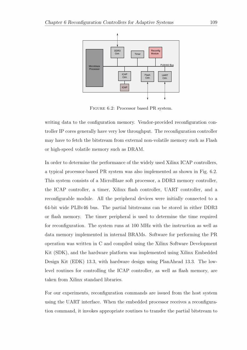
Chapter 6 Reconfiguration Controllers for Adaptive Systems 109
MicroblazeProcessor
PLB/AXI Bus
DDR3 Ctrlr.
ICAP Ctrlr.
ICAP
Timer
Flash Ctrlr.
ReconfigModule
UARTCtrlr.
Figure 6.2: Processor based PR system.
writing data to the configuration memory. Vendor-provided reconfiguration con-
troller IP cores generally have very low throughput. The reconfiguration controller
may have to fetch the bitstream from external non-volatile memory such as Flash
or high-speed volatile memory such as DRAM.
In order to determine the performance of the widely used Xilinx ICAP controllers,
a typical processor-based PR system was also implemented as shown in Fig. 6.2.
This system consists of a MicroBlaze soft processor, a DDR3 memory controller,
the ICAP controller, a timer, Xilinx flash controller, UART controller, and a
reconfigurable module. All the peripheral devices were initially connected to a
64-bit wide PLBv46 bus. The partial bitstreams can be stored in either DDR3
or flash memory. The timer peripheral is used to determine the time required
for reconfiguration. The system runs at 100 MHz with the instruction as well as
data memory implemented in internal BRAMs. Software for performing the PR
operation was written in C and compiled using the Xilinx Software Development
Kit (SDK), and the hardware platform was implemented using Xilinx Embedded
Design Kit (EDK) 13.3, with hardware design using PlanAhead 13.3. The low-
level routines for controlling the ICAP controller, as well as flash memory, are
taken from Xilinx standard libraries.
For our experiments, reconfiguration commands are issued from the host system
using the UART interface. When the embedded processor receives a reconfigura-
tion command, it invokes appropriate routines to transfer the partial bitstream to
Chapter 6 Reconfiguration Controllers for Adaptive Systems 110
the ICAP controller depending upon its storage location. The timer reports the to-
tal number of clock cycles required for the operation to complete, and from this, the
throughput can be determined. For the PLB system, Xilinx’s XPS HWICAP [16]
was used as the ICAP controller. When the bitstreams are stored in flash memory,
the reconfiguration throughput is only 0.47 MB/s and when stored in the DDR3
memory, the throughput is 8.4 MB/s. These values prove that present processor-
based ICAP controllers are unsuitable for time-critical reconfiguration scenarios.
The same experiment was repeated using the latest AXI-bus based design. In
this system, the DDR3 controller is connected to an AXI4 bus and other pe-
ripherals to AXI4-lite bus. The ICAP controller used in this experiment is the
AXI HWICAP [125]. When using the AXI-bus, performance improves slightly.
Reconfiguration throughput using flash memory is 0.49 MB/s, and using DDR3
memory gives 9.1 MB/s. These values are still well below what is theoretically
possible.
Reconfiguration management involves deciding when and which specific partial
bitstreams are required for changing the system’s configuration. It also includes
passing the required information regarding the partial bitstreams (such as bit-
stream size, location etc.) to the reconfiguration controller. To enable better
flexibility, this is usually implemented in software. For systems that do not imple-
ment a processor in the FPGA, an external processor is required to manage this
operation. The major bottleneck for these systems is the communication overhead
between the control and data planes due to their loosely-coupled architecture. In
Chapter 8, we discuss the communication and reconfiguration management in such
systems in detail, with reference to a PR testbed framework.
In traditional FPGA based adaptive systems, reconfiguration management can also
be implemented purely in hardware. Such systems implement simple reconfigura-
tion decision making based on predefined operating conditions such as temperature
or signal-to-noise ratio. The number of configurations supported by such a sys-
tem will be limited since the partial bitstreams are pre-fetched to on-board volatile
Chapter 6 Reconfiguration Controllers for Adaptive Systems 111
memory. Overall reconfiguration management might be implemented using a state
machine, that encodes changes in system operating conditions.
6.3 Related Work
Traditionally, the reconfiguration operation is controlled by a processor, through
a vendor-provided ICAP controller such as the OPBHWICAP or XPSHWICAP,
connected as a slave device to the processor bus [126, 16]. Using these vendor-
provided controllers gives low throughput in the region of 4.6-10.1 MB/s [127, 108].
The ICAP hard macro itself, however, supports speeds of up to 400 MB/s (32 bits
at 100 MHz).
In [128], the authors propose connecting the ICAP controller to the fast simplex
link (FSL) bus of a Microblaze soft processor. The drawback is that the processor
becomes consumed with the task of requesting configuration data from external
memory and sending it over the FSL bus. The resulting throughput of under
30 MB/s remains well below the theoretical limit of the ICAP.
Using DMA to transfer partial bitstreams from external memory has previously
been shown to be effective in increasing throughput [129], but there, the authors
do not discuss how bitstreams are initially stored in the external memory. Else-
where, some have tried to achieve better performance by over-clocking the ICAP
primitive [130]. Since the maximum frequency at which the controller can operate
depends upon manufacturing variability and specific placement and routing, this
would need to be determined on a device-by-device basis, which is cumbersome.
Other work on optimised ICAP controllers has often made unrealistic assump-
tions, such as the complete configuration bitstream being stored in FPGA Block
RAMs [108]. This is not practical, as FPGAs have limited memory that is of-
ten insufficient for even a small number of bitstreams, and these memories are
often required for system implementation. We have found no work that abstracts
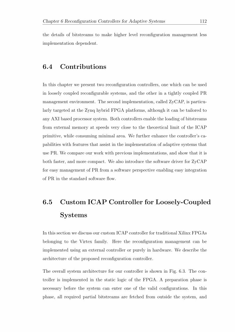
Chapter 6 Reconfiguration Controllers for Adaptive Systems 112
the details of bitstreams to make higher level reconfiguration management less
implementation dependent.
6.4 Contributions
In this chapter we present two reconfiguration controllers, one which can be used
in loosely coupled reconfigurable systems, and the other in a tightly coupled PR
management environment. The second implementation, called ZyCAP, is particu-
larly targeted at the Zynq hybrid FPGA platforms, although it can be tailored to
any AXI based processor system. Both controllers enable the loading of bitstreams
from external memory at speeds very close to the theoretical limit of the ICAP
primitive, while consuming minimal area. We further enhance the controller’s ca-
pabilities with features that assist in the implementation of adaptive systems that
use PR. We compare our work with previous implementations, and show that it is
both faster, and more compact. We also introduce the software driver for ZyCAP
for easy management of PR from a software perspective enabling easy integration
of PR in the standard software flow.
6.5 Custom ICAP Controller for Loosely-Coupled
Systems
In this section we discuss our custom ICAP controller for traditional Xilinx FPGAs
belonging to the Virtex family. Here the reconfiguration management can be
implemented using an external controller or purely in hardware. We describe the
architecture of the proposed reconfiguration controller.
The overall system architecture for our controller is shown in Fig. 6.3. The con-
troller is implemented in the static logic of the FPGA. A preparation phase is
necessary before the system can enter one of the valid configurations. In this
phase, all required partial bitstreams are fetched from outside the system, and
Chapter 6 Reconfiguration Controllers for Adaptive Systems 113
UART6I/F
Statistics
FIFOI/F
Conf.PointerBuffer
DMACtrl.
ICAPCtrl.
ICAP
8256
256
32
25664DDR
Ctrl.DRAM
Memory
To/From6Host
FPGA
Figure 6.3: Custom ICAP controller system architecture showing differentfunctional blocks and connectivity.
stored in external DRAM memory. These bitstreams may originate from a file
system on some non-volatile storage, or alternatively be sent from a host PC. In
the latter case, we can use a simple interface such as UART, as this preparation
phase is not time-critical. The bitstreams are read in over this interface, then
pushed through a DMA controller into the external memory, while storing their
location labels in a Configuration Pointer Buffer for later use. Once preparation
is complete, the system is operational and can now autonomously load partial bit-
streams and reconfigure regions. This involves the transfer of partial bitstreams
from the external memory to the ICAP controller using the DMA controller.
6.5.1 DDR Memory Controller
The DDR controller controls the external memory based on the commands from
the DMA controller. This is a DDR3 controller, which controls a 64-bit wide
external memory. This core is generated using Xilinx’s memory interface generator
(MIG) wizard [131]. The core’s read and write data ports are 256 bits wide and
run at 200 MHz.
Chapter 6 Reconfiguration Controllers for Adaptive Systems 114
6.5.2 DMA Controller
The DMA controller is an important component in this system, and is largely
responsible for the high speed. This block performs a DMA write operation to
store partial bitstreams in the external memory during the preparation phase, as
well as reading the bitstreams from memory when reconfiguring regions in the
runtime phase. Before storing a partial bitstream to memory, the host configures
the DMA transfer length and the starting memory location at which to store
the bitstream. During reconfiguration operations, the DMA controller instructs
the memory controller to generate memory read sequences, until the specified
number of bytes are read. To achieve high throughput, the controller issues back-
to-back read commands. For read operations, the address and data length can
be obtained either from a host system, or from the configuration pointer buffer.
The DMA controller and the memory controller coordinate their operations using
a producer-consumer model handshake.
6.5.3 FIFO Interface
Partial bitstreams are temporarily stored in a FIFO before being loaded into the
external memory from the host system during the preparation phase. This in-
terface serves two purposes: the host interface can be changed without affecting
the remainder of the system, and data can be packed, allowing the host interface
width to be different from the data width of the system memory interface. At
present, UART data comes in one byte at a time and the memory controller write
width is 32 bytes; this difference is accommodated by the FIFO interface.
6.5.4 Configuration Pointer Buffer
This buffer stores the sizes of the partial bitstreams as well as their starting lo-
cations in the external memory. These parameters are stored automatically when
the DMA controller transfers partial bitstreams to the external memory in the
Chapter 6 Reconfiguration Controllers for Adaptive Systems 115
preparation phase. Each set of parameters has a reference number, which is their
ordinal number of transfer from the host system. The advantage of using this
buffer is that when the system is in the runtime phase, a reconfiguration manager
can load partial bitstreams using just their pointer label, rather than it having
to be aware of any further bitstream details. The DMA engine configurations
as well as programming sequences are done automatically by the state machine
controlling this buffer.
6.5.5 Statistics
The statistics block contains two hardware counters for system performance moni-
toring. The first counter measures the overall performance by measuring the num-
ber of clock cycles required for reconfiguration to complete after the command is
issued. The second counter measures the performance of the ICAP controller. The
values present in these registers can be accessed from a host system through the
UART interface, or used within the rest of the adaptive system. The presence of
hardware counters provides precise system performance measures in comparison to
inaccurate software counters, and can be used by the adaptive control for efficient
system management.
Another parameter monitored by this block is the number of times each partial bit-
stream is used for reconfiguration. In an adaptive system scenario, this information
gives an overview of the conditions in which the system is operating, since different
partial bitstreams are used depending upon system conditions. This information
could be used to further optimise PR design details, such as the partitioning, or
improve performance through configuration prefetching [132].
6.5.6 ICAP Controller
The detailed architecture of the ICAP controller is shown in Fig. 6.4. It consists
of an asynchronous FIFO, clock manager, ICAP control state machine and the
ICAP hardmacro. The asynchronous FIFO is used to temporarily store the partial
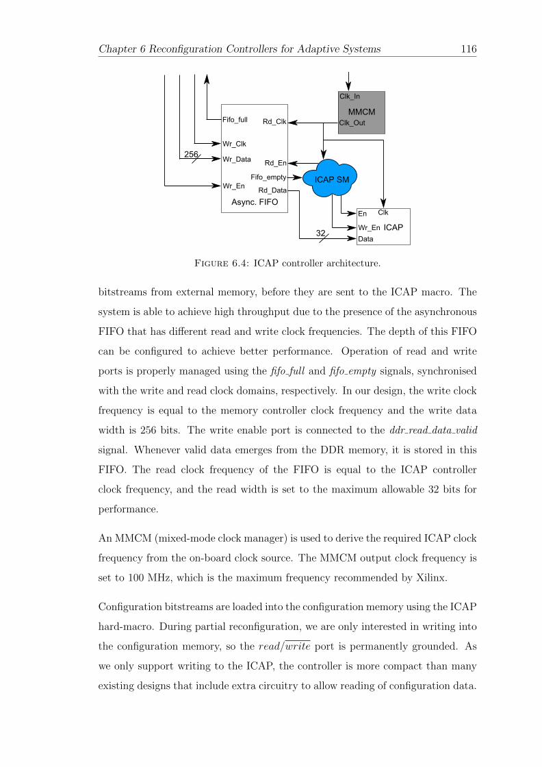
Chapter 6 Reconfiguration Controllers for Adaptive Systems 116
Figure 6.4: ICAP controller architecture.
bitstreams from external memory, before they are sent to the ICAP macro. The
system is able to achieve high throughput due to the presence of the asynchronous
FIFO that has different read and write clock frequencies. The depth of this FIFO
can be configured to achieve better performance. Operation of read and write
ports is properly managed using the fifo full and fifo empty signals, synchronised
with the write and read clock domains, respectively. In our design, the write clock
frequency is equal to the memory controller clock frequency and the write data
width is 256 bits. The write enable port is connected to the ddr read data valid
signal. Whenever valid data emerges from the DDR memory, it is stored in this
FIFO. The read clock frequency of the FIFO is equal to the ICAP controller
clock frequency, and the read width is set to the maximum allowable 32 bits for
performance.
An MMCM (mixed-mode clock manager) is used to derive the required ICAP clock
frequency from the on-board clock source. The MMCM output clock frequency is
set to 100 MHz, which is the maximum frequency recommended by Xilinx.
Configuration bitstreams are loaded into the configuration memory using the ICAP
hard-macro. During partial reconfiguration, we are only interested in writing into
the configuration memory, so the read/write port is permanently grounded. As
we only support writing to the ICAP, the controller is more compact than many
existing designs that include extra circuitry to allow reading of configuration data.
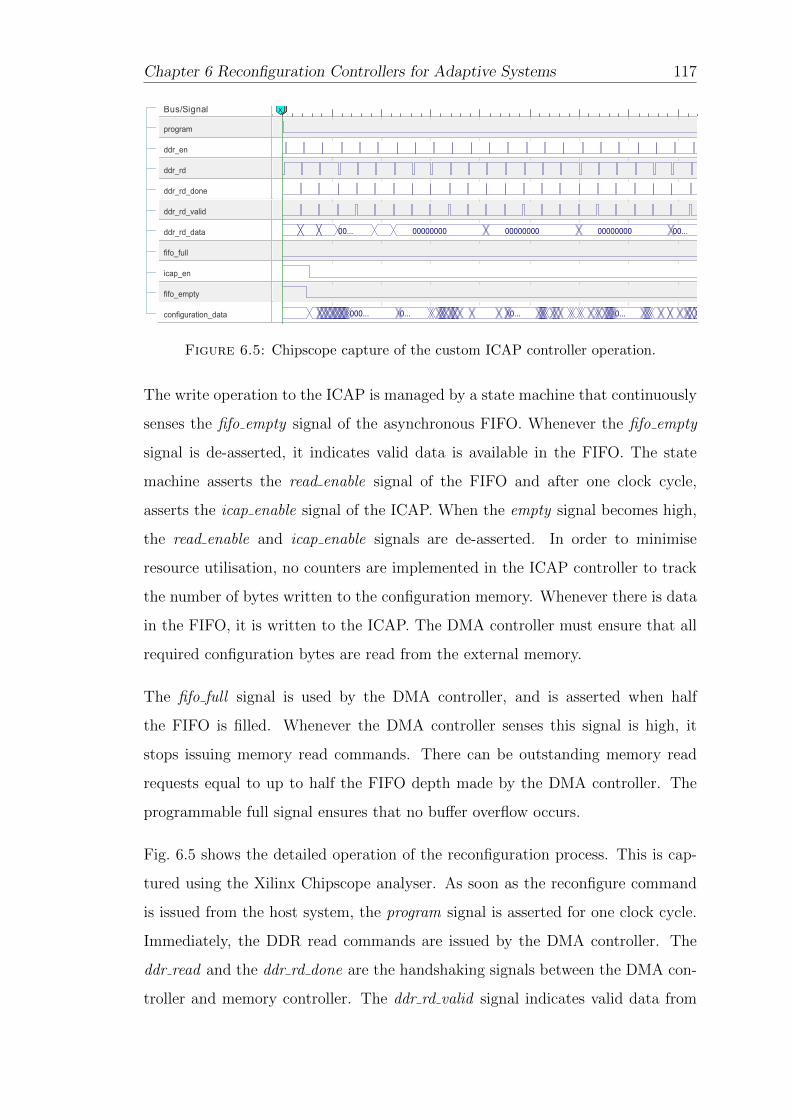
Chapter 6 Reconfiguration Controllers for Adaptive Systems 117
Bus/Signal OTX
program
ddr_en
ddr_rd
ddr_rd_done
ddr_rd_valid
ddr_rd_data 00... 00000000 00000000 00000000 00...
fifo_full
icap_en
fifo_empty
configuration_data 000... 0... 0... 0...
Figure 6.5: Chipscope capture of the custom ICAP controller operation.
The write operation to the ICAP is managed by a state machine that continuously
senses the fifo empty signal of the asynchronous FIFO. Whenever the fifo empty
signal is de-asserted, it indicates valid data is available in the FIFO. The state
machine asserts the read enable signal of the FIFO and after one clock cycle,
asserts the icap enable signal of the ICAP. When the empty signal becomes high,
the read enable and icap enable signals are de-asserted. In order to minimise
resource utilisation, no counters are implemented in the ICAP controller to track
the number of bytes written to the configuration memory. Whenever there is data
in the FIFO, it is written to the ICAP. The DMA controller must ensure that all
required configuration bytes are read from the external memory.
The fifo full signal is used by the DMA controller, and is asserted when half
the FIFO is filled. Whenever the DMA controller senses this signal is high, it
stops issuing memory read commands. There can be outstanding memory read
requests equal to up to half the FIFO depth made by the DMA controller. The
programmable full signal ensures that no buffer overflow occurs.
Fig. 6.5 shows the detailed operation of the reconfiguration process. This is cap-
tured using the Xilinx Chipscope analyser. As soon as the reconfigure command
is issued from the host system, the program signal is asserted for one clock cycle.
Immediately, the DDR read commands are issued by the DMA controller. The
ddr read and the ddr rd done are the handshaking signals between the DMA con-
troller and memory controller. The ddr rd valid signal indicates valid data from
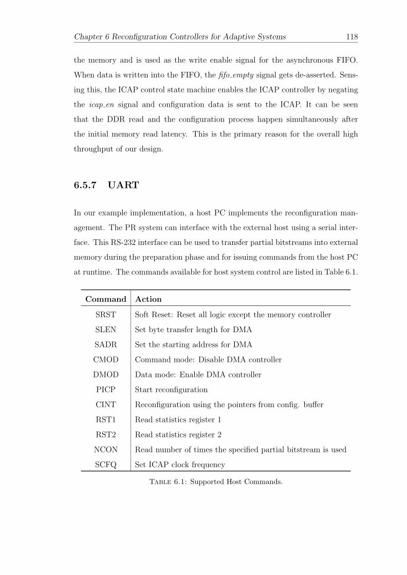
Chapter 6 Reconfiguration Controllers for Adaptive Systems 118
the memory and is used as the write enable signal for the asynchronous FIFO.
When data is written into the FIFO, the fifo empty signal gets de-asserted. Sens-
ing this, the ICAP control state machine enables the ICAP controller by negating
the icap en signal and configuration data is sent to the ICAP. It can be seen
that the DDR read and the configuration process happen simultaneously after
the initial memory read latency. This is the primary reason for the overall high
throughput of our design.
6.5.7 UART
In our example implementation, a host PC implements the reconfiguration man-
agement. The PR system can interface with the external host using a serial inter-
face. This RS-232 interface can be used to transfer partial bitstreams into external
memory during the preparation phase and for issuing commands from the host PC
at runtime. The commands available for host system control are listed in Table 6.1.
Command Action
SRST Soft Reset: Reset all logic except the memory controller
SLEN Set byte transfer length for DMA
SADR Set the starting address for DMA
CMOD Command mode: Disable DMA controller
DMOD Data mode: Enable DMA controller
PICP Start reconfiguration
CINT Reconfiguration using the pointers from config. buffer
RST1 Read statistics register 1
RST2 Read statistics register 2
NCON Read number of times the specified partial bitstream is used
SCFQ Set ICAP clock frequency
Table 6.1: Supported Host Commands.
Chapter 6 Reconfiguration Controllers for Adaptive Systems 119
6.5.8 Using the Dynamic Reconfiguration Port (DRP)
Researchers have tried over-clocking the ICAP to achieve higher performance.
According to Xilinx, the maximum clock frequency at which ICAP is guaranteed
to correctly operate is 100 MHz. It has been reported that the ICAP can run
at up to 550 MHz [130]. However, this maximum clock frequency depends upon
the device speed grade, manufacturing variability, and detailed custom placement
and routing. A clock frequency which is suitable for one specific FPGA may
not be suitable for another, even with the same speed grade, and Xilinx does
not guarantee proper ICAP operation above 100 MHz. Clock generating circuits
cannot be modified using PR, since Xilinx requires that all the clock modifying
components such as phase locked loops (PLLs) and digital clock managers (DCMs)
reside in the static region. In order to overcome this issue, we make use of a
feature available in the Virtex-6 MMCM known as the dynamic reconfiguration
port (DRP).
The DRP makes it possible to configure the output frequency of the MMCM at
runtime. This is achieved by modifying the internal registers of the MMCM using
the DRP. Hence, we start operation of our controller at 100 MHz. Subsequently,
the operating frequency is increased, until the reconfiguration process fails. The
operating frequency is then fixed at just below the failing frequency.
In our initial implementation the clock frequency must be manually tuned by
issuing commands from the host system. We have enhanced this feature in a sub-
sequent implementation, with the operating frequency dynamically changed based
on the output of an on-chip temperature sensor. When the chip core temperature
is below a predefined threshold value (40◦C), the ICAP is clocked close to 200
MHz and when the temperature exceeds this value, the clock frequency is reduced
to 100 MHz. This overclocking capability can allow us to achieve throughputs
beyond the 400 MB/s theoretical maximum supported at 100 MHz.
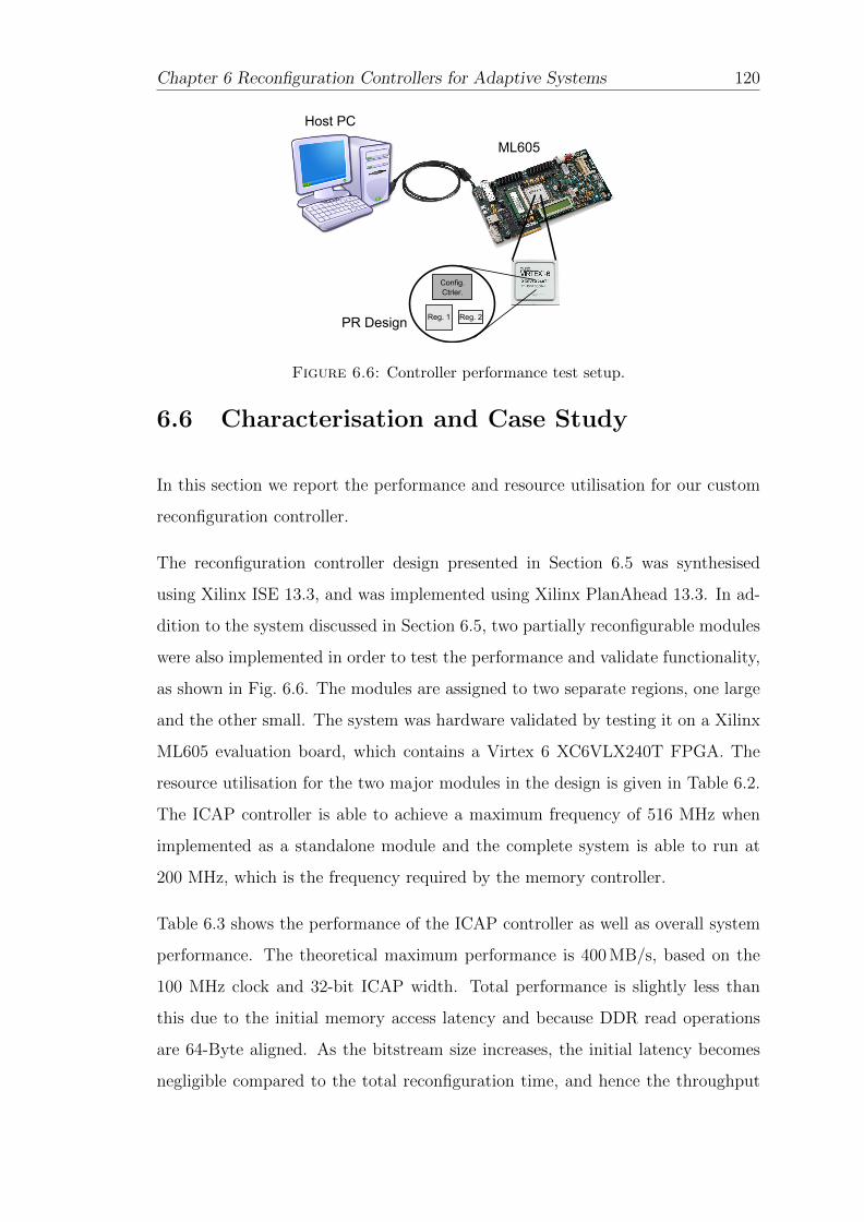
Chapter 6 Reconfiguration Controllers for Adaptive Systems 120
Config. Ctrler.
Reg. 1 Reg. 2
Host PC
ML605
PR Design
Figure 6.6: Controller performance test setup.
6.6 Characterisation and Case Study
In this section we report the performance and resource utilisation for our custom
reconfiguration controller.
The reconfiguration controller design presented in Section 6.5 was synthesised
using Xilinx ISE 13.3, and was implemented using Xilinx PlanAhead 13.3. In ad-
dition to the system discussed in Section 6.5, two partially reconfigurable modules
were also implemented in order to test the performance and validate functionality,
as shown in Fig. 6.6. The modules are assigned to two separate regions, one large
and the other small. The system was hardware validated by testing it on a Xilinx
ML605 evaluation board, which contains a Virtex 6 XC6VLX240T FPGA. The
resource utilisation for the two major modules in the design is given in Table 6.2.
The ICAP controller is able to achieve a maximum frequency of 516 MHz when
implemented as a standalone module and the complete system is able to run at
200 MHz, which is the frequency required by the memory controller.
Table 6.3 shows the performance of the ICAP controller as well as overall system
performance. The theoretical maximum performance is 400 MB/s, based on the
100 MHz clock and 32-bit ICAP width. Total performance is slightly less than
this due to the initial memory access latency and because DDR read operations
are 64-Byte aligned. As the bitstream size increases, the initial latency becomes
negligible compared to the total reconfiguration time, and hence the throughput
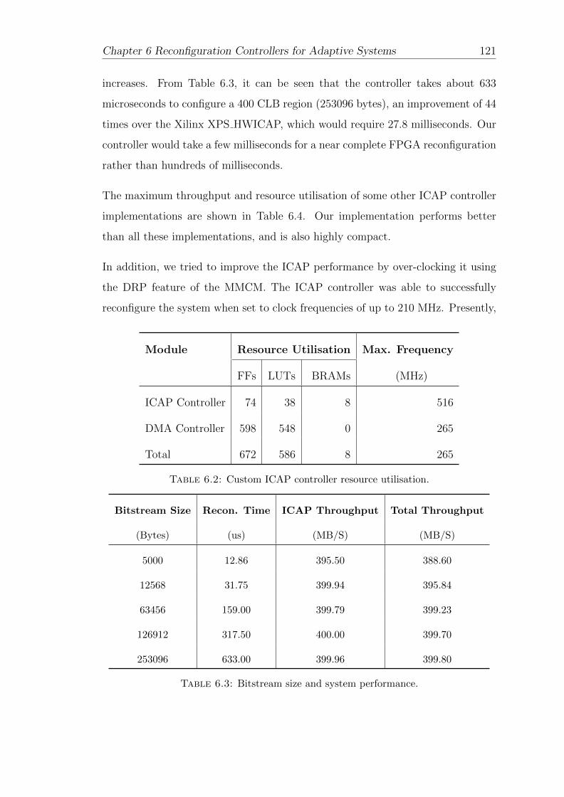
Chapter 6 Reconfiguration Controllers for Adaptive Systems 121
increases. From Table 6.3, it can be seen that the controller takes about 633
microseconds to configure a 400 CLB region (253096 bytes), an improvement of 44
times over the Xilinx XPS HWICAP, which would require 27.8 milliseconds. Our
controller would take a few milliseconds for a near complete FPGA reconfiguration
rather than hundreds of milliseconds.
The maximum throughput and resource utilisation of some other ICAP controller
implementations are shown in Table 6.4. Our implementation performs better
than all these implementations, and is also highly compact.
In addition, we tried to improve the ICAP performance by over-clocking it using
the DRP feature of the MMCM. The ICAP controller was able to successfully
reconfigure the system when set to clock frequencies of up to 210 MHz. Presently,
Module Resource Utilisation Max. Frequency
FFs LUTs BRAMs (MHz)
ICAP Controller 74 38 8 516
DMA Controller 598 548 0 265
Total 672 586 8 265
Table 6.2: Custom ICAP controller resource utilisation.
Bitstream Size Recon. Time ICAP Throughput Total Throughput
(Bytes) (us) (MB/S) (MB/S)
5000 12.86 395.50 388.60
12568 31.75 399.94 395.84
63456 159.00 399.79 399.23
126912 317.50 400.00 399.70
253096 633.00 399.96 399.80
Table 6.3: Bitstream size and system performance.
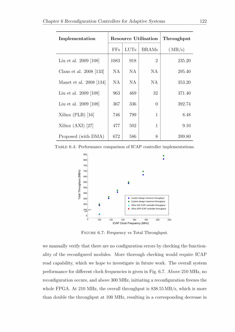
Chapter 6 Reconfiguration Controllers for Adaptive Systems 122
Implementation Resource Utilisation Throughput
FFs LUTs BRAMs ( MB/s)
Liu et al. 2009 [108] 1083 918 2 235.20
Claus et al. 2008 [133] NA NA NA 295.40
Manet et al. 2008 [134] NA NA NA 353.20
Liu et al. 2009 [108] 963 469 32 371.40
Liu et al. 2009 [108] 367 336 0 392.74
Xilinx (PLB) [16] 746 799 1 8.48
Xilinx (AXI) [27] 477 502 1 9.10
Proposed (with DMA) 672 586 8 399.80
Table 6.4: Performance comparison of ICAP controller implementations.
100 120 140 160 180 200 220
350
400
450
500
550
600
650
700
750
800
850
0
5
ICAP Clock Frequency (MHz)
Tot
al T
hrou
ghpu
t (M
B/s
)
Custom design minimum throughput
Custom design maximum throughput
Xilinx AXI ICAP controller throughput
Xilinx XPS ICAP controller throughput
Figure 6.7: Frequency vs Total Throughput.
we manually verify that there are no configuration errors by checking the function-
ality of the reconfigured modules. More thorough checking would require ICAP
read capability, which we hope to investigate in future work. The overall system
performance for different clock frequencies is given in Fig. 6.7. Above 210 MHz, no
reconfiguration occurs, and above 300 MHz, initiating a reconfiguration freezes the
whole FPGA. At 210 MHz, the overall throughput is 838.55 MB/s, which is more
than double the throughput at 100 MHz, resulting in a corresponding decrease in
Chapter 6 Reconfiguration Controllers for Adaptive Systems 123
reconfiguration time.
6.7 ZyCAP: A Reconfiguration Controller for Tightly
Coupled Adaptive Systems
In this section we discuss our reconfiguration controller specially targeting Zynq
Hybrid FPGAs. On the Zynq, The PL can be reconfigured from the PS or from
within the PL itself. The PS uses the device configuration interface (DevC), which
has a dedicated DMA controller to transfer bitstreams from external memory to
the PCAP (processor configuration access port) for reconfiguration. The Zynq also
has an ICAP primitive in the PL, as found in other Xilinx FPGAs. The ICAP has
a 32-bit, 100MHz streaming interface, providing up to 400 MB/s reconfiguration
throughput.
Officially, Xilinx supports two schemes for PR on the Zynq, one through the PCAP
and the other through the ICAP. By specifying the starting location and size, the
library function XDcfg TransferBitfile() can be used to transfer PR bitstreams
from external memory (DRAM) to the PCAP. The main advantage of this scheme
is that it does not require any PL resources and gives a moderate reconfiguration
throughput of 128 MB/s. The main drawback is that it blocks the processor during
reconfiguration, precluding overlapped execution and reconfiguration.
Xilinx also provides an IP core (AXI HWICAP) and library function (XHw-
Icap DeviceWrite()) to enable PR using the ICAP. The AXI-Lite interface of the
core is used to connect it to the PS through a GP port. Since this method is not
DMA based, throughput is only 19 MB/s. This approach also blocks the processor,
and is hence inferior to the PCAP approach.
We have modified the ICAP approach by interfacing the hard DMA controller
in the PS with the AXI HWICAP IP and writing a custom driver function. An
interrupt from the DMA controller is used to indicate completion of reconfigura-
tion. The achievable throughput in such a case is 67 MB/s, which is significantly
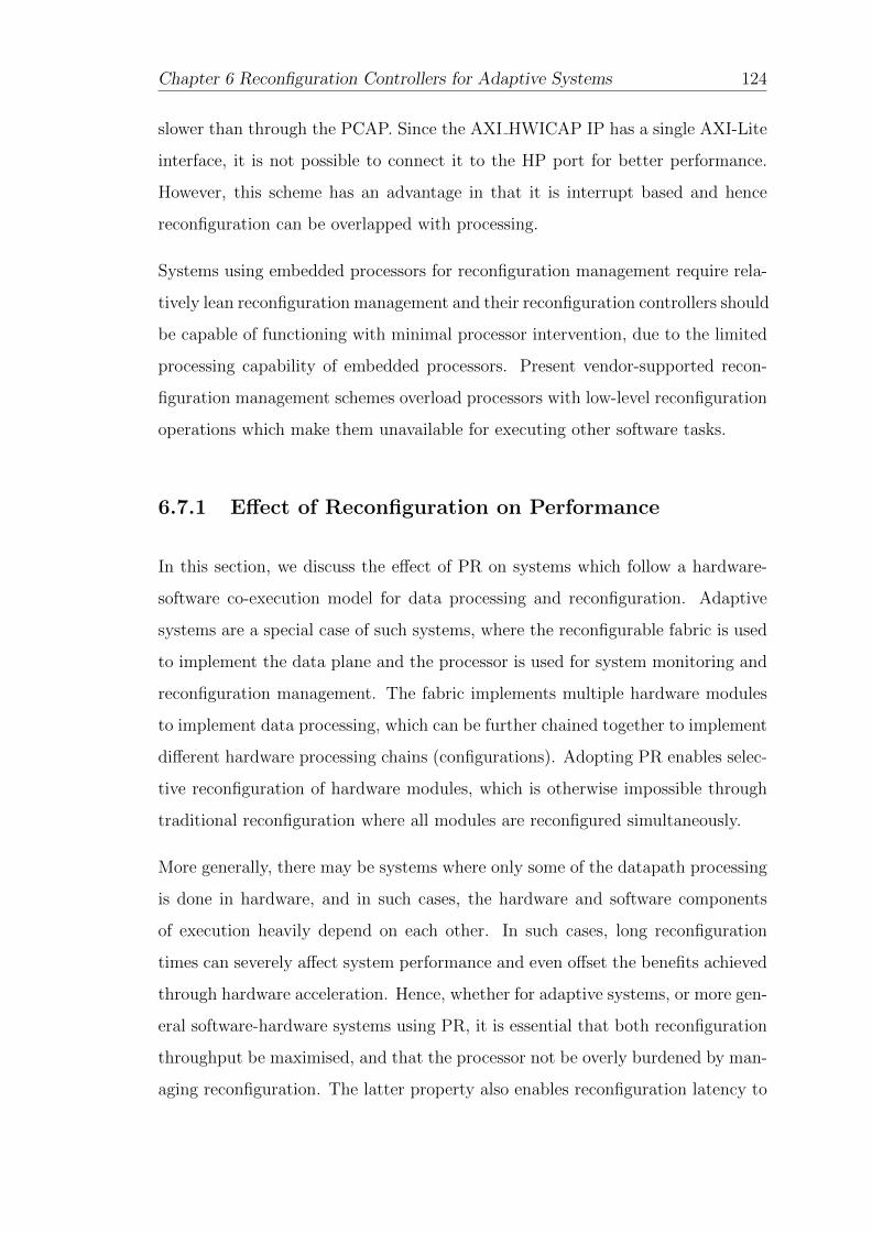
Chapter 6 Reconfiguration Controllers for Adaptive Systems 124
slower than through the PCAP. Since the AXI HWICAP IP has a single AXI-Lite
interface, it is not possible to connect it to the HP port for better performance.
However, this scheme has an advantage in that it is interrupt based and hence
reconfiguration can be overlapped with processing.
Systems using embedded processors for reconfiguration management require rela-
tively lean reconfiguration management and their reconfiguration controllers should
be capable of functioning with minimal processor intervention, due to the limited
processing capability of embedded processors. Present vendor-supported recon-
figuration management schemes overload processors with low-level reconfiguration
operations which make them unavailable for executing other software tasks.
6.7.1 Effect of Reconfiguration on Performance
In this section, we discuss the effect of PR on systems which follow a hardware-
software co-execution model for data processing and reconfiguration. Adaptive
systems are a special case of such systems, where the reconfigurable fabric is used
to implement the data plane and the processor is used for system monitoring and
reconfiguration management. The fabric implements multiple hardware modules
to implement data processing, which can be further chained together to implement
different hardware processing chains (configurations). Adopting PR enables selec-
tive reconfiguration of hardware modules, which is otherwise impossible through
traditional reconfiguration where all modules are reconfigured simultaneously.
More generally, there may be systems where only some of the datapath processing
is done in hardware, and in such cases, the hardware and software components
of execution heavily depend on each other. In such cases, long reconfiguration
times can severely affect system performance and even offset the benefits achieved
through hardware acceleration. Hence, whether for adaptive systems, or more gen-
eral software-hardware systems using PR, it is essential that both reconfiguration
throughput be maximised, and that the processor not be overly burdened by man-
aging reconfiguration. The latter property also enables reconfiguration latency to
Chapter 6 Reconfiguration Controllers for Adaptive Systems 125
Setup Config Control DataIn Compute DataOut
Tsetup Tconfig Tcontrol Tdatain Tcompute Tdataout
Figure 6.8: Task profile for implementing hardware acceleration [136].
be hidden to a certain extent, by overlapping reconfiguration with execution of
other software tasks.
To understand the impact of PR on the performance of such software-hardware
systems, consider the typical profile for an hardware task execution as depicted
in Fig. 6.8. The system configures the hardware module on the fabric, sends in-
put data, triggers execution, then reads back the output after execution. Tsetup
is the time taken to decide whether a reconfiguration is required, Tconfig is the
reconfiguration time, Tcontrol is the time taken to trigger the hardware, Tdatain is
the time to send data to the hardware, Tcompute is the hardware execution time
and Tdataout is the time for the results to be read back. This profile shows that
efficient management functions are paramount in maximising the benefits offered
by hardware acceleration. Tdatain and Tdataout depend upon the system architecture
and how data movement is managed. Tcontrol is usually negligible, involving reg-
ister configurations. A PR system should minimise Tsetup , while also maximising
reconfiguration throughput to minimise Tconfig . If the processor is used to manage
all the reconfiguration steps, then it is not available for other tasks. This is espe-
cially true when the number of hardware tasks and frequency of reconfiguration
increases [135].
The desire is that the processor handles only high-level reconfiguration manage-
ment while the lower level mechanics are managed separately. The advantage of
this approach is that execution of tasks on the processor and reconfiguration of
the PL can be overlapped. Fig. 6.9 shows the profile for an application compris-
ing two software and two hardware tasks executed alternately. In Fig. 6.9(a), the
processor manages configuration, and so must wait for this to complete before
executing its software tasks. Fig. 6.9(b), shows how the overall execution time is
reduced when the processor is only tasked with initiating the reconfiguration. The
reconfigurable region can be blanked when no hardware is used to reduce power

Chapter 6 Reconfiguration Controllers for Adaptive Systems 126
Processor Task 1 C1 Idle Task 2 C2 Idle
Execution time
Hardware module Idle C1 Task1 Idle C2 Task2
(a)Processor Task 1 Idle Task 2 Idle
Hardware module Blnk C1 Task1 B Blnk C2 Task2
(b)Processor Task 1 Task 2 Idle
Hardware module C1 Task1 C2 Task2
(c)
Figure 6.9: Effect of overlapping hardware and software execution. (a) Pro-cessing and reconfiguration happening sequentially. C1 and C2 represent hard-ware reconfigurations with the PRR configured with a new bitstream. (b)Reconfiguration in parallel with processing for dependent tasks. B representsblanking the PRR and Blnk represent a blanked PR region. (c) Software andhardware running independent tasks with minimal software management over-
head.
consumption without compromising system performance. In Fig. 6.9(c) we show
the potential gains for independent tasks; now that the processor is freed from
low-level configuration management, it can continue with other tasks (subject to
dependencies).
6.7.2 ZyCAP PR Controller
To achieve maximum reconfiguration performance, we have developed a custom
controller, called ZyCAP, and an associated driver, to verify whether such a solu-
tion can improve on PCAP performance, while reducing processor PR management
overhead. As discussed in the Section 6.6, our experiments with traditional FPGAs
such as the Virtex-6 showed that a custom solution can provide near theoretical
peak reconfiguration throughput. But that custom controller was designed for
non-processor systems, and hence did not provide a software-centric view, making
it difficult to port to the Zynq.
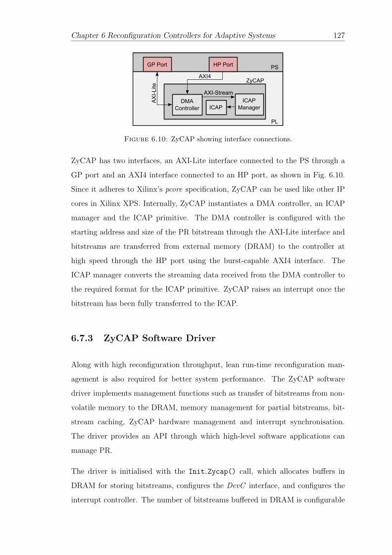
Chapter 6 Reconfiguration Controllers for Adaptive Systems 127
GP Port HP Port
DMAController
ICAP Manager
PS
PL
ZyCAP
AX
I-Li
te
AXI4
AXI-Stream
ICAP
Figure 6.10: ZyCAP showing interface connections.
ZyCAP has two interfaces, an AXI-Lite interface connected to the PS through a
GP port and an AXI4 interface connected to an HP port, as shown in Fig. 6.10.
Since it adheres to Xilinx’s pcore specification, ZyCAP can be used like other IP
cores in Xilinx XPS. Internally, ZyCAP instantiates a DMA controller, an ICAP
manager and the ICAP primitive. The DMA controller is configured with the
starting address and size of the PR bitstream through the AXI-Lite interface and
bitstreams are transferred from external memory (DRAM) to the controller at
high speed through the HP port using the burst-capable AXI4 interface. The
ICAP manager converts the streaming data received from the DMA controller to
the required format for the ICAP primitive. ZyCAP raises an interrupt once the
bitstream has been fully transferred to the ICAP.
6.7.3 ZyCAP Software Driver
Along with high reconfiguration throughput, lean run-time reconfiguration man-
agement is also required for better system performance. The ZyCAP software
driver implements management functions such as transfer of bitstreams from non-
volatile memory to the DRAM, memory management for partial bitstreams, bit-
stream caching, ZyCAP hardware management and interrupt synchronisation.
The driver provides an API through which high-level software applications can
manage PR.
The driver is initialised with the Init Zycap() call, which allocates buffers in
DRAM for storing bitstreams, configures the DevC interface, and configures the
interrupt controller. The number of bitstreams buffered in DRAM is configurable
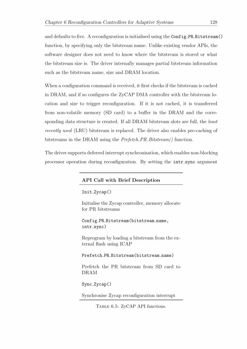
Chapter 6 Reconfiguration Controllers for Adaptive Systems 128
and defaults to five. A reconfiguration is initialised using the Config PR Bitstream()
function, by specifying only the bitstream name. Unlike existing vendor APIs, the
software designer does not need to know where the bitstream is stored or what
the bitstream size is. The driver internally manages partial bitstream information
such as the bitstream name, size and DRAM location.
When a configuration command is received, it first checks if the bitstream is cached
in DRAM, and if so configures the ZyCAP DMA controller with the bitstream lo-
cation and size to trigger reconfiguration. If it is not cached, it is transferred
from non-volatile memory (SD card) to a buffer in the DRAM and the corre-
sponding data structure is created. If all DRAM bitstream slots are full, the least
recently used (LRU) bitstream is replaced. The driver also enables pre-caching of
bitstreams in the DRAM using the Prefetch PR Bitstream() function.
The driver supports deferred interrupt synchronisation, which enables non-blocking
processor operation during reconfiguration. By setting the intr sync argument
API Call with Brief Description
Init Zycap()
Initialise the Zycap controller, memory allocatefor PR bitstreams
Config PR Bitstream(bitstream name,
intr sync)
Reprogram by loading a bitstream from the ex-ternal flash using ICAP
Prefetch PR Bitstream(bitstream name)
Prefetch the PR bitstream from SD card toDRAM
Sync Zycap()
Synchronise Zycap reconfiguration interrupt
Table 6.5: ZyCAP API functions.
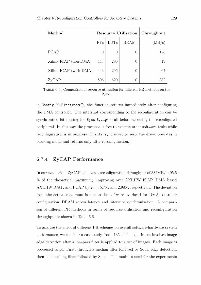
Chapter 6 Reconfiguration Controllers for Adaptive Systems 129
Method Resource Utilisation Throughput
FFs LUTs BRAMs (MB/s)
PCAP 0 0 0 128
Xilinx ICAP (non-DMA) 443 296 0 19
Xilinx ICAP (with DMA) 443 296 0 67
ZyCAP 806 620 0 382
Table 6.6: Comparison of resource utilisation for different PR methods on theZynq.
in Config PR Bitstream(), the function returns immediately after configuring
the DMA controller. The interrupt corresponding to the reconfiguration can be
synchronised later using the Sync Zycap() call before accessing the reconfigured
peripheral. In this way the processor is free to execute other software tasks while
reconfiguration is in progress. If intr sync is set to zero, the driver operates in
blocking mode and returns only after reconfiguration.
6.7.4 ZyCAP Performance
In our evaluation, ZyCAP achieves a reconfiguration throughput of 382MB/s (95.5
% of the theoretical maximum), improving over AXI HW ICAP, DMA based
AXI HW ICAP, and PCAP by 20×, 5.7×, and 2.98×, respectively. The deviation
from theoretical maximum is due to the software overhead for DMA controller
configuration, DRAM access latency and interrupt synchronisation. A compari-
son of different PR methods in terms of resource utilisation and reconfiguration
throughput is shown in Table 6.6.
To analyse the effect of different PR schemes on overall software-hardware system
performance, we consider a case study from [136]. The experiment involves image
edge detection after a low-pass filter is applied to a set of images. Each image is
processed twice. First, through a median filter followed by Sobel edge detection,
then a smoothing filter followed by Sobel. The modules used for the experiments

Chapter 6 Reconfiguration Controllers for Adaptive Systems 130
Parameter Desig. Value (Sec.)
Decision time Tsetup 0
Reconfiguration time Tconfig 0.970/T
Transfer of control time Tcontrol 1.12× 10⁻⁶
Data send time Tdatain (B/382)× 10−6
Compute time Tcompute 0
Data receive time Tdataout (B/128)× 10−6
Table 6.7: Timing parameters for the Case study.
are reconfigured sequentially in a single PRR. An image is first transferred from
external memory to a processing core and the processed image is streamed back
to the memory via DMA. After each step, the output is analysed by the processor
for quality checks.
For our experiments, we use the ZedBoard [137].The PRR size is 2300 CLBs, 60
DSP blocks and 50 BRAMs, large enough to accommodate the largest module
(smoothing filter). The partial bitstream size is 1,018,080 Bytes while a full Zynq
bitstream would be 4,045,564 Bytes. A DMA controller is used to transfer data
between the external memory and the processing core through an HP port and
a hardware timer is interfaced for accurate performance measurement. All PL
components run at 100MHz. The hardware and software for this evaluation are
developed using Xilinx’s EDK 14.6 and PlanAhead 14.6 software versions.
DMA transfers between the external memory and the PRR are measured at
382 MB/s. Throughput between the processor and the external memory is 128 MB/s.
The latency for accessing a peripheral from the processor is 140ns. To configure
the DMA controller and manage data movement, 8 registers are configured by
the processor, consuming 1.12us. These map to the execution time parameters
described in Section 6.7 as shown in Table 6.7 for processing B Bytes of data at a
reconfiguration speed of T MB/s.
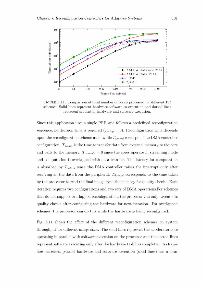
Chapter 6 Reconfiguration Controllers for Adaptive Systems 131
32 64 128 256 512 1024 2048 4096
104
105
106
107
108
Frame Size (pixels)
Throughput(p
ixels/sec)
AXI HWICAP(non-DMA)
AXI HWICAP(DMA)
PCAP
ZyCAP
Figure 6.11: Comparison of total number of pixels processed for different PRschemes. Solid lines represent hardware-software co-execution and dotted lines
represent sequential hardware and software execution.
Since this application uses a single PRR and follows a predefined reconfiguration
sequence, no decision time is required (Tsetup = 0). Reconfiguration time depends
upon the reconfiguration scheme used, while Tcontrol corresponds to DMA controller
configuration. Tdatain is the time to transfer data from external memory to the core
and back to the memory. Tcompute = 0 since the cores operate in streaming mode
and computation is overlapped with data transfer. The latency for computation
is absorbed by Tdatain since the DMA controller raises the interrupt only after
receiving all the data from the peripheral. Tdataout corresponds to the time taken
by the processor to read the final image from the memory for quality checks. Each
iteration requires two configurations and two sets of DMA operations.For schemes
that do not support overlapped reconfiguration, the processor can only execute its
quality checks after configuring the hardware for next iteration. For overlapped
schemes, the processor can do this while the hardware is being reconfigured.
Fig. 6.11 shows the effect of the different reconfiguration schemes on system
throughput for different image sizes. The solid lines represent the accelerator core
operating in parallel with software execution on the processor and the dotted-lines
represent software executing only after the hardware task has completed. As frame
size increases, parallel hardware and software execution (solid lines) has a clear
Chapter 6 Reconfiguration Controllers for Adaptive Systems 132
benefit. In these cases, when the software execution time is smaller than the re-
configuration time, the PCAP based method has a significant advantage over the
DMA based AXI HWICAP due to its higher throughput. However, as the data
size increases (above 512×512 pixels), overlapped reconfiguration becomes more
important, and the DMA based AXI HWICAP outperforms the PCAP method
since software execution time is now comparable to reconfiguration time. For
large frame sizes, the performance of the DMA based methods converges since the
reconfiguration time begins to diminish with regard to software execution time.
The same is true for blocking non-DMA based methods, but they saturate at a
lower overall throughput. At an image size of 512×512, ZyCAP increases applica-
tion throughput by 11.35×, 3.28×, and 2.96×, over AXI HW ICAP, DMA based
AXI HW ICAP, and PCAP, respectively.
6.8 Summary
In this chapter we discussed the role of reconfiguration controllers in achieving bet-
ter system performance for PR-based adaptive systems. We presented two custom
reconfiguration controllers, which significantly improve reconfiguration through-
put in traditional FPGAs and hybrid FPGAs like the Zynq. The reconfiguration
controller for loosely coupled architectures is later adapted to develop a PR hard-
ware verification platform as discussed in Chapter 8. The ZyCAP device driver
presented allows overlapped execution and reconfiguration, resulting in improved
overall system performance for mixed software-hardware systems. The ZyCAP
hardware can be similarly used with soft processors like the Microblaze, but driver
software modifications are required for interrupt management. ZyCap also plays
a significant role in automating PR development on hybrid FPGAs as discussed
in Chapter 7.
Both the reconfiguration controllers are released in the public domain, for use by
researchers intending to incorporate PR into their systems, allowing the focus to
be on the application rather than optimisations of PR mechanisms.
Chapter 7
An Automated PR Tool-flow for
Adaptive Systems
7.1 Introduction
A fully automated flow that allows adaptive systems designers to map applications
to a PR design without the need for FPGA expertise has so far failed to materialise.
We believe this is an essential step in PR achieving more widespread adoption, as
it is the application experts who can best identify the scenarios that make sense
for PR, and use it within the context of realistic applications. Although models
have been proposed for mapping adaptive system descriptions to FPGAs, actual
implementation of the resulting systems remains challenging [138, 139]. As it
stands, FPGA experts come up with small, unrealistic example applications that
fail to capture the interest of application designers.
The tools and techniques we have discussed so far focussed on individual aspects
of PR including design time optimisations and reconfiguration control techniques.
In this chapter we propose a framework which integrates these to create an au-
tomated tool-flow, which maps a high-level system description into a hardware
implementation and generates the required management software. The run-time
management of adaptive systems is also explained in detail. We believe that for
133
Chapter 7 An Automated PR Tool-flow for Adaptive Systems 134
low-level device architecture-dependent operations, such as place and route and
bitstream generation, vendor tools provide superior performance compared to cus-
tom tools. They also avoid problems with porting and incompatibilities as new
devices are released. Hence, instead of circumventing the limitations imposed by
these tools, our framework respects these constraints, making it portable as the
architectures and tool-flows evolve.
We concentrate on the new Xilinx Zynq hybrid FPGAs as the target implementa-
tion platform due to their tightly coupled processor-fabric architecture. Compute-
intensive configurations can be implemented on the reconfigurable fabric while
complex adaptation algorithms can be implemented in software, making them
easily programmable. This work is the first fully automated flow for mapping high-
level descriptions of adaptive systems to hybrid FPGAs. This co-design framework
for PR is called CoPR for Zynq.
The work presented in this chapter has also been discussed in:
• K. Vipin and S. A. Fahmy, Enabling High Level Design of Adaptive Systems
with Partial Reconfiguration, PhD Forum Poster, in Proceedings of the Inter-
national Conference on Field Programmable Technology (FPT), New Delhi,
2011 [140].
• K. Vipin and S. A. Fahmy, Automated Partial Reconfiguration Design for
Adaptive Systems with CoPR for Zynq, in Proceedings of the International
Conference on Field Programmable Custom Computing Machines (FCCM),
Boston, Massachusetts, May 2014, pp. 202–205 [141].
7.2 Contributions
1. An automated end-to-end tool flow for PR based adaptive systems, suitable
for non experts, that maps high-level system descriptions to a real imple-
mentation on hybrid FPGAs.

Chapter 7 An Automated PR Tool-flow for Adaptive Systems 135
External Event
Control plane
Control loop
Event Action
Data plane
M1Data In Data Out
M2 M3 M4
Figure 7.1: The control and data planes of an adaptive system. The twoplanes interact through events and actions. M1, M2, M3, and M4 represent
different hardware modules and the dataflow is from left to right.
2. A runtime configuration manager that provides an API for describing adap-
tation through the abstraction, with automated seamless management of the
PR process.
Our framework can equally serve as the implementation basis for other techniques
like time-mutliplexing of task graphs, where configurations are statically deter-
mined.
7.3 Mapping Dynamically Adaptive Systems
This section describes different aspects of adaptive systems and their mapping
onto hybrid-FPGAs. First, we describe the adaptive system model and define
the terms used, along with our tool flow. Then we explain the integration of our
custom tools with the vendor PR implementation tool chain.
7.3.1 System Decomposition
The system level architecture for adaptive systems we have chosen is depicted in
Fig. 7.1. The overall system is divided into two logical planes, namely the control
plane and the data plane. The configurations, that complete data processing,
are within the data plane while the control plane monitors and regulates system
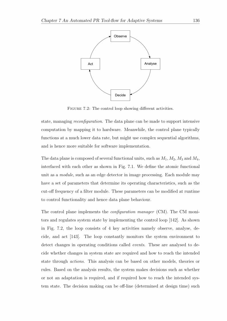
Chapter 7 An Automated PR Tool-flow for Adaptive Systems 136
Observe
Analyse
Decide
Act
Figure 7.2: The control loop showing different activities.
state, managing reconfiguration. The data plane can be made to support intensive
computation by mapping it to hardware. Meanwhile, the control plane typically
functions at a much lower data rate, but might use complex sequential algorithms,
and is hence more suitable for software implementation.
The data plane is composed of several functional units, such asM1,M2,M3 andM4,
interfaced with each other as shown in Fig. 7.1. We define the atomic functional
unit as a module, such as an edge detector in image processing. Each module may
have a set of parameters that determine its operating characteristics, such as the
cut-off frequency of a filter module. These parameters can be modified at runtime
to control functionality and hence data plane behaviour.
The control plane implements the configuration manager (CM). The CM moni-
tors and regulates system state by implementing the control loop [142]. As shown
in Fig. 7.2, the loop consists of 4 key activities namely observe, analyse, de-
cide, and act [143]. The loop constantly monitors the system environment to
detect changes in operating conditions called events. These are analysed to de-
cide whether changes in system state are required and how to reach the intended
state through actions. This analysis can be based on other models, theories or
rules. Based on the analysis results, the system makes decisions such as whether
or not an adaptation is required, and if required how to reach the intended sys-
tem state. The decision making can be off-line (determined at design time) such
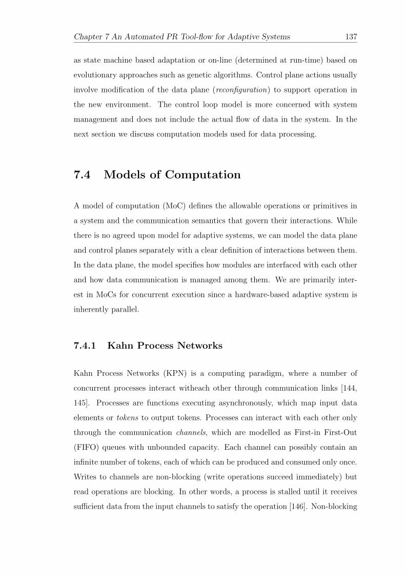
Chapter 7 An Automated PR Tool-flow for Adaptive Systems 137
as state machine based adaptation or on-line (determined at run-time) based on
evolutionary approaches such as genetic algorithms. Control plane actions usually
involve modification of the data plane (reconfiguration) to support operation in
the new environment. The control loop model is more concerned with system
management and does not include the actual flow of data in the system. In the
next section we discuss computation models used for data processing.
7.4 Models of Computation
A model of computation (MoC) defines the allowable operations or primitives in
a system and the communication semantics that govern their interactions. While
there is no agreed upon model for adaptive systems, we can model the data plane
and control planes separately with a clear definition of interactions between them.
In the data plane, the model specifies how modules are interfaced with each other
and how data communication is managed among them. We are primarily inter-
est in MoCs for concurrent execution since a hardware-based adaptive system is
inherently parallel.
7.4.1 Kahn Process Networks
Kahn Process Networks (KPN) is a computing paradigm, where a number of
concurrent processes interact witheach other through communication links [144,
145]. Processes are functions executing asynchronously, which map input data
elements or tokens to output tokens. Processes can interact with each other only
through the communication channels, which are modelled as First-in First-Out
(FIFO) queues with unbounded capacity. Each channel can possibly contain an
infinite number of tokens, each of which can be produced and consumed only once.
Writes to channels are non-blocking (write operations succeed immediately) but
read operations are blocking. In other words, a process is stalled until it receives
sufficient data from the input channels to satisfy the operation [146]. Non-blocking
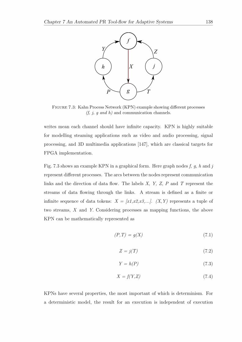
Chapter 7 An Automated PR Tool-flow for Adaptive Systems 138
g
f
h jX
YZ
TP
Figure 7.3: Kahn Process Network (KPN) example showing different processes(f, j, g and h) and communication channels.
writes mean each channel should have infinite capacity. KPN is highly suitable
for modelling steaming applications such as video and audio processing, signal
processing, and 3D multimedia applications [147], which are classical targets for
FPGA implementation.
Fig. 7.3 shows an example KPN in a graphical form. Here graph nodes f, g, h and j
represent different processes. The arcs between the nodes represent communication
links and the direction of data flow. The labels X, Y, Z, P and T represent the
streams of data flowing through the links. A stream is defined as a finite or
infinite sequence of data tokens: X = [x1,x2,x3,...]. (X,Y) represents a tuple of
two streams, X and Y. Considering processes as mapping functions, the above
KPN can be mathematically represented as
(P,T) = g(X) (7.1)
Z = j(T) (7.2)
Y = h(P) (7.3)
X = f(Y,Z) (7.4)
KPNs have several properties, the most important of which is determinism. For
a deterministic model, the result for an execution is independent of execution
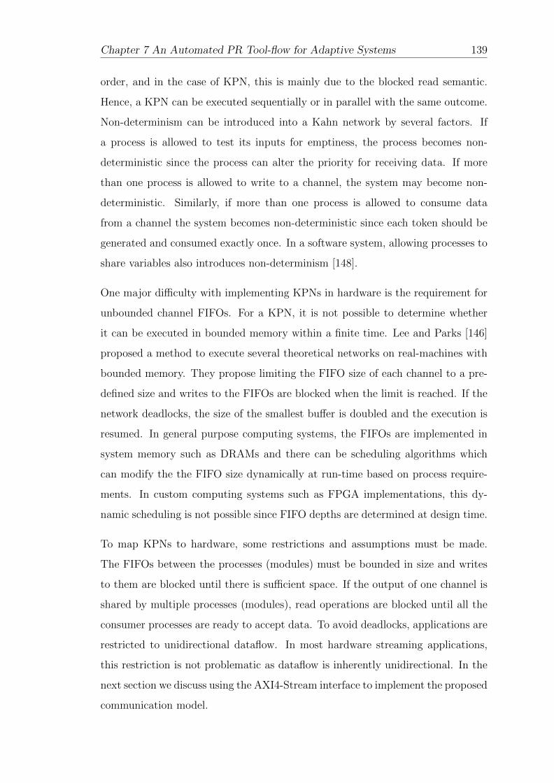
Chapter 7 An Automated PR Tool-flow for Adaptive Systems 139
order, and in the case of KPN, this is mainly due to the blocked read semantic.
Hence, a KPN can be executed sequentially or in parallel with the same outcome.
Non-determinism can be introduced into a Kahn network by several factors. If
a process is allowed to test its inputs for emptiness, the process becomes non-
deterministic since the process can alter the priority for receiving data. If more
than one process is allowed to write to a channel, the system may become non-
deterministic. Similarly, if more than one process is allowed to consume data
from a channel the system becomes non-deterministic since each token should be
generated and consumed exactly once. In a software system, allowing processes to
share variables also introduces non-determinism [148].
One major difficulty with implementing KPNs in hardware is the requirement for
unbounded channel FIFOs. For a KPN, it is not possible to determine whether
it can be executed in bounded memory within a finite time. Lee and Parks [146]
proposed a method to execute several theoretical networks on real-machines with
bounded memory. They propose limiting the FIFO size of each channel to a pre-
defined size and writes to the FIFOs are blocked when the limit is reached. If the
network deadlocks, the size of the smallest buffer is doubled and the execution is
resumed. In general purpose computing systems, the FIFOs are implemented in
system memory such as DRAMs and there can be scheduling algorithms which
can modify the the FIFO size dynamically at run-time based on process require-
ments. In custom computing systems such as FPGA implementations, this dy-
namic scheduling is not possible since FIFO depths are determined at design time.
To map KPNs to hardware, some restrictions and assumptions must be made.
The FIFOs between the processes (modules) must be bounded in size and writes
to them are blocked until there is sufficient space. If the output of one channel is
shared by multiple processes (modules), read operations are blocked until all the
consumer processes are ready to accept data. To avoid deadlocks, applications are
restricted to unidirectional dataflow. In most hardware streaming applications,
this restriction is not problematic as dataflow is inherently unidirectional. In the
next section we discuss using the AXI4-Stream interface to implement the proposed
communication model.
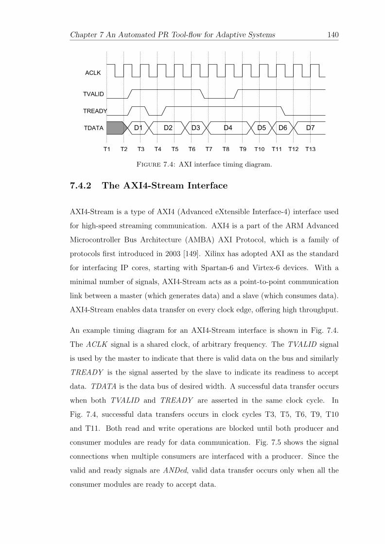
Chapter 7 An Automated PR Tool-flow for Adaptive Systems 140
ACLK
TVALID
TREADY
TDATA D1 D2 D3 D4 D5 D6 D7
T8T7T6T5T4T3T2T1 T11T10T9 T13T12
Figure 7.4: AXI interface timing diagram.
7.4.2 The AXI4-Stream Interface
AXI4-Stream is a type of AXI4 (Advanced eXtensible Interface-4) interface used
for high-speed streaming communication. AXI4 is a part of the ARM Advanced
Microcontroller Bus Architecture (AMBA) AXI Protocol, which is a family of
protocols first introduced in 2003 [149]. Xilinx has adopted AXI as the standard
for interfacing IP cores, starting with Spartan-6 and Virtex-6 devices. With a
minimal number of signals, AXI4-Stream acts as a point-to-point communication
link between a master (which generates data) and a slave (which consumes data).
AXI4-Stream enables data transfer on every clock edge, offering high throughput.
An example timing diagram for an AXI4-Stream interface is shown in Fig. 7.4.
The ACLK signal is a shared clock, of arbitrary frequency. The TVALID signal
is used by the master to indicate that there is valid data on the bus and similarly
TREADY is the signal asserted by the slave to indicate its readiness to accept
data. TDATA is the data bus of desired width. A successful data transfer occurs
when both TVALID and TREADY are asserted in the same clock cycle. In
Fig. 7.4, successful data transfers occurs in clock cycles T3, T5, T6, T9, T10
and T11. Both read and write operations are blocked until both producer and
consumer modules are ready for data communication. Fig. 7.5 shows the signal
connections when multiple consumers are interfaced with a producer. Since the
valid and ready signals are ANDed, valid data transfer occurs only when all the
consumer modules are ready to accept data.
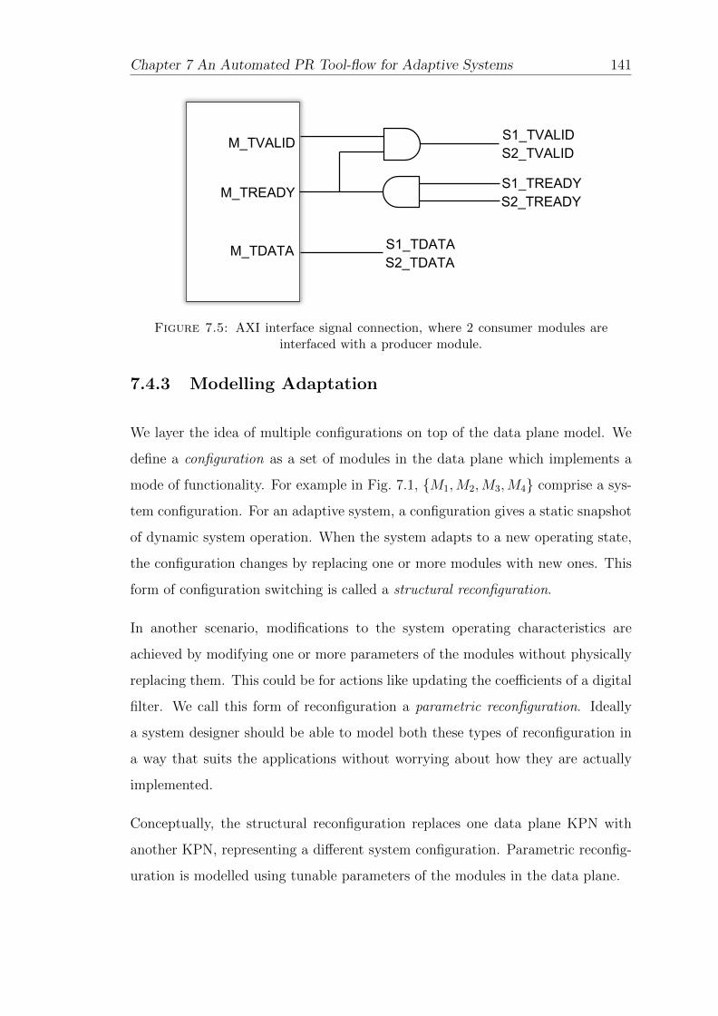
Chapter 7 An Automated PR Tool-flow for Adaptive Systems 141
M_TVALID
M_TREADY
M_TDATA
S1_TREADYS2_TREADY
S1_TVALIDS2_TVALID
S1_TDATAS2_TDATA
Figure 7.5: AXI interface signal connection, where 2 consumer modules areinterfaced with a producer module.
7.4.3 Modelling Adaptation
We layer the idea of multiple configurations on top of the data plane model. We
define a configuration as a set of modules in the data plane which implements a
mode of functionality. For example in Fig. 7.1, {M1,M2,M3,M4} comprise a sys-
tem configuration. For an adaptive system, a configuration gives a static snapshot
of dynamic system operation. When the system adapts to a new operating state,
the configuration changes by replacing one or more modules with new ones. This
form of configuration switching is called a structural reconfiguration.
In another scenario, modifications to the system operating characteristics are
achieved by modifying one or more parameters of the modules without physically
replacing them. This could be for actions like updating the coefficients of a digital
filter. We call this form of reconfiguration a parametric reconfiguration. Ideally
a system designer should be able to model both these types of reconfiguration in
a way that suits the applications without worrying about how they are actually
implemented.
Conceptually, the structural reconfiguration replaces one data plane KPN with
another KPN, representing a different system configuration. Parametric reconfig-
uration is modelled using tunable parameters of the modules in the data plane.
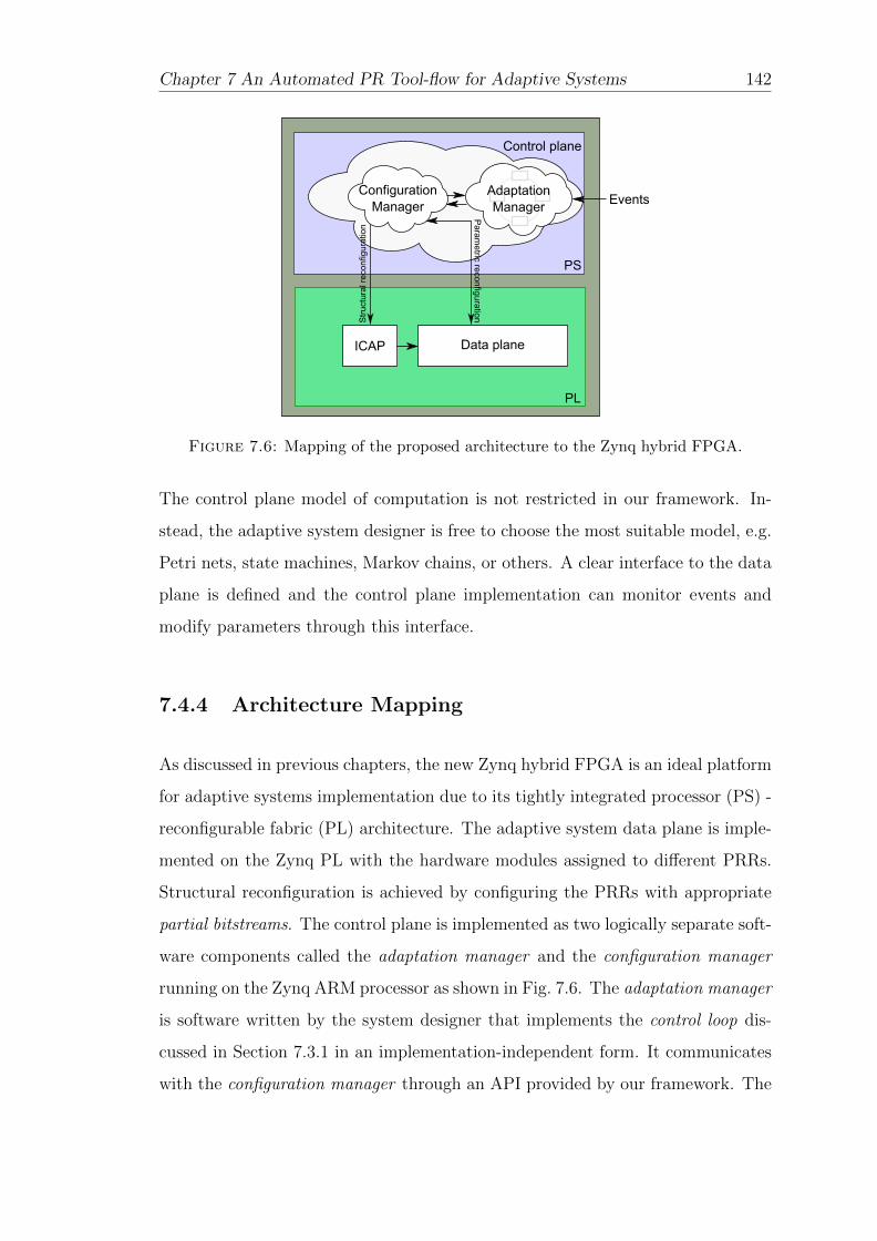
Chapter 7 An Automated PR Tool-flow for Adaptive Systems 142
ConfigurationManager
ConfigurationManager
PS
PL
Events
ICAP
Control plane
Data planeS
truc
tura
l rec
onfig
urat
ion
Para
metric reconfiguration
Adaptation Manager
Figure 7.6: Mapping of the proposed architecture to the Zynq hybrid FPGA.
The control plane model of computation is not restricted in our framework. In-
stead, the adaptive system designer is free to choose the most suitable model, e.g.
Petri nets, state machines, Markov chains, or others. A clear interface to the data
plane is defined and the control plane implementation can monitor events and
modify parameters through this interface.
7.4.4 Architecture Mapping
As discussed in previous chapters, the new Zynq hybrid FPGA is an ideal platform
for adaptive systems implementation due to its tightly integrated processor (PS) -
reconfigurable fabric (PL) architecture. The adaptive system data plane is imple-
mented on the Zynq PL with the hardware modules assigned to different PRRs.
Structural reconfiguration is achieved by configuring the PRRs with appropriate
partial bitstreams. The control plane is implemented as two logically separate soft-
ware components called the adaptation manager and the configuration manager
running on the Zynq ARM processor as shown in Fig. 7.6. The adaptation manager
is software written by the system designer that implements the control loop dis-
cussed in Section 7.3.1 in an implementation-independent form. It communicates
with the configuration manager through an API provided by our framework. The
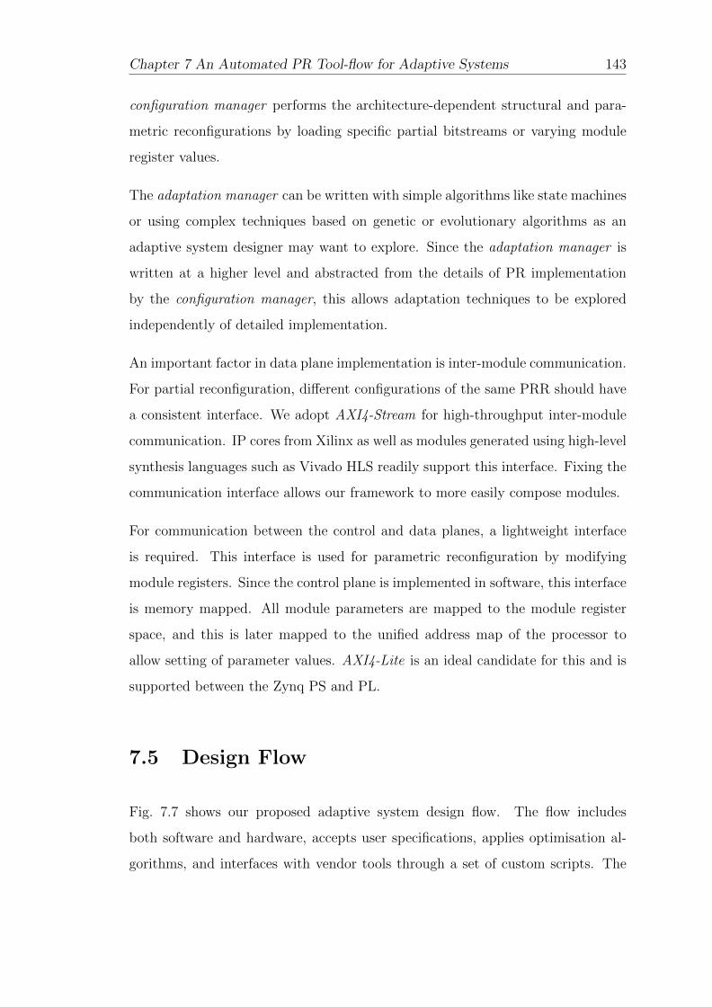
Chapter 7 An Automated PR Tool-flow for Adaptive Systems 143
configuration manager performs the architecture-dependent structural and para-
metric reconfigurations by loading specific partial bitstreams or varying module
register values.
The adaptation manager can be written with simple algorithms like state machines
or using complex techniques based on genetic or evolutionary algorithms as an
adaptive system designer may want to explore. Since the adaptation manager is
written at a higher level and abstracted from the details of PR implementation
by the configuration manager, this allows adaptation techniques to be explored
independently of detailed implementation.
An important factor in data plane implementation is inter-module communication.
For partial reconfiguration, different configurations of the same PRR should have
a consistent interface. We adopt AXI4-Stream for high-throughput inter-module
communication. IP cores from Xilinx as well as modules generated using high-level
synthesis languages such as Vivado HLS readily support this interface. Fixing the
communication interface allows our framework to more easily compose modules.
For communication between the control and data planes, a lightweight interface
is required. This interface is used for parametric reconfiguration by modifying
module registers. Since the control plane is implemented in software, this interface
is memory mapped. All module parameters are mapped to the module register
space, and this is later mapped to the unified address map of the processor to
allow setting of parameter values. AXI4-Lite is an ideal candidate for this and is
supported between the Zynq PS and PL.
7.5 Design Flow
Fig. 7.7 shows our proposed adaptive system design flow. The flow includes
both software and hardware, accepts user specifications, applies optimisation al-
gorithms, and interfaces with vendor tools through a set of custom scripts. The
Chapter 7 An Automated PR Tool-flow for Adaptive Systems 144
AdaptationAPIs
Configuration.Specification
ModuleLibrary
Resource.calculation
Partitioning
Floorplanning
Hardware.Integration
PAR.and.BitGen
config..Manager
Software.integration
Reconfig..Controller
Software.compilation
Hardware Flow Software Flow
AdaptationSpecification
Bitstreams Software.executable
User Vendor.tools Framework
Figure 7.7: Proposed design flow for PR based adaptive systems design, show-ing steps performed by the user, vendor tools and the framework.
adaptive system designer describes the overall system as a composition of mod-
ules from a library of parameterised modules, or custom modules designed to the
required interface specification. They also describe how the system should adapt
between different valid configurations in software. Our tool takes these descrip-
tions and creates a working partially reconfigurable system without the designer
needing to work at the detailed hardware level. We adapt our previous parti-
tioning and floorplanning algorithms discussed in Chapters 4 and 5 to develop an
integrated tool-flow and add automated mapping to Zynq hybrid FPGAs. The
following sections describe each step in more detail.
7.5.1 Specification
The primary designer inputs to the proposed framework are the configuration and
adaptation specifications. The configuration specification details the different valid
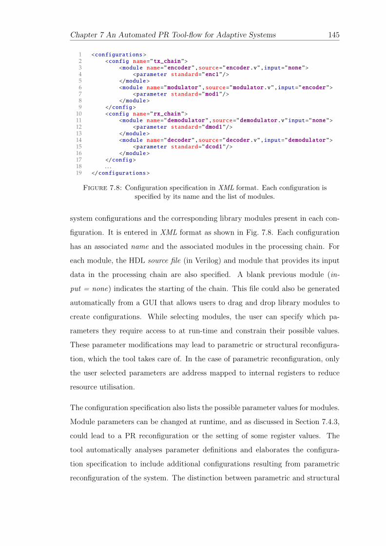
Chapter 7 An Automated PR Tool-flow for Adaptive Systems 145
1 <configurations >2 <config name="tx_chain">3 <module name="encoder",source="encoder.v",input="none">4 <parameter standard="enc1"/>5 </module>6 <module name="modulator",source="modulator.v",input="encoder">7 <parameter standard="mod1"/>8 </module>9 </config>
10 <config name="rx_chain">11 <module name="demodulator",source="demodulator.v"input="none">12 <parameter standard="dmod1"/>13 </module>14 <module name="decoder",source="decoder.v",input="demodulator">15 <parameter standard="dcod1"/>16 </module>17 </config>18 . . .19 </configurations >
Figure 7.8: Configuration specification in XML format. Each configuration isspecified by its name and the list of modules.
system configurations and the corresponding library modules present in each con-
figuration. It is entered in XML format as shown in Fig. 7.8. Each configuration
has an associated name and the associated modules in the processing chain. For
each module, the HDL source file (in Verilog) and module that provides its input
data in the processing chain are also specified. A blank previous module (in-
put = none) indicates the starting of the chain. This file could also be generated
automatically from a GUI that allows users to drag and drop library modules to
create configurations. While selecting modules, the user can specify which pa-
rameters they require access to at run-time and constrain their possible values.
These parameter modifications may lead to parametric or structural reconfigura-
tion, which the tool takes care of. In the case of parametric reconfiguration, only
the user selected parameters are address mapped to internal registers to reduce
resource utilisation.
The configuration specification also lists the possible parameter values for modules.
Module parameters can be changed at runtime, and as discussed in Section 7.4.3,
could lead to a PR reconfiguration or the setting of some register values. The
tool automatically analyses parameter definitions and elaborates the configura-
tion specification to include additional configurations resulting from parametric
reconfiguration of the system. The distinction between parametric and structural
Chapter 7 An Automated PR Tool-flow for Adaptive Systems 146
reconfiguration is thus abstracted from the designer’s point of view, so that they
have a unified model for reconfiguration.
The adaptation specification contains the software code for the adaptation manager
described in Section 7.4.4. Since the low-level configuration management details
are transparent to the adaptation manager, it can be independently developed
based on the configurations specified in the configuration specification. Users
can choose the adaptation technique of their choice and integrate it with the
reconfiguration manager using the provided software API. Sample state machine
adaptation manager templates are provided to assist developers.
Based on the configuration specification, the framework first uses the vendor syn-
thesis tool (XST) to synthesise all the modules for the target FPGA, to determine
resource requirements. Scripts extract the number of CLBs, DSP blocks and Block
RAMs from the synthesis reports and these numbers are later used for design par-
titioning and floorplanning.
7.5.2 Partitioning and Interface Generation
The partitioning step involves determining the number of reconfigurable regions
(PRRs) and allocating modules to them. The way the system is partitioned greatly
influences resource requirements and reconfiguration time, as we explored in Chap-
ter 4. We apply the algorithm proposed in Chapter 4, targeting minimised total
reconfigurable area to reduce reconfiguration time and system dynamic power. A
detailed description of this algorithm is presented in Section 4.7.
After partitioning, wrapper modules that instantiate the modules in each parti-
tion and configuration are generated, ensuring a unified interface across different
configurations. A pr system top wrapper is also generated which instantiates and
connects all the PRRs as black boxes. The generated wrapper module is in IP
core format, which can be directly imported to Xilinx’s XPS tool. As detailed in
Section 7.4.4, using a consistent interface (AXI4-Stream and AXI4-Lite) across all
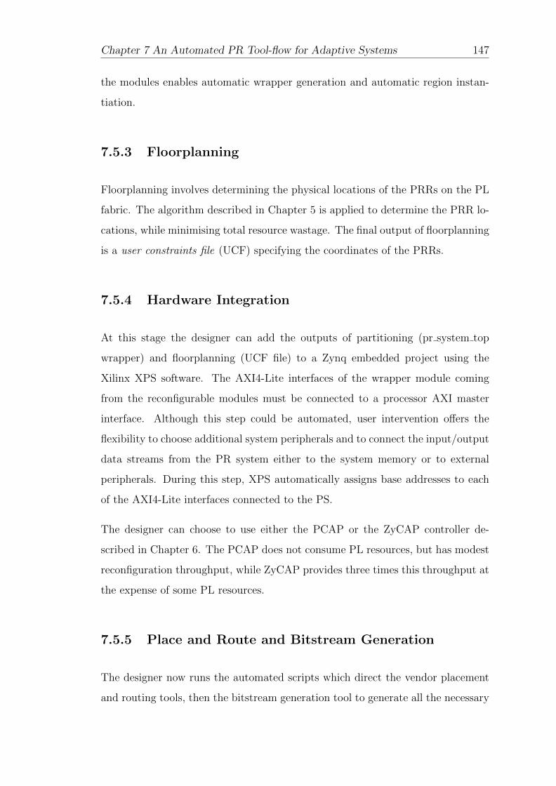
Chapter 7 An Automated PR Tool-flow for Adaptive Systems 147
the modules enables automatic wrapper generation and automatic region instan-
tiation.
7.5.3 Floorplanning
Floorplanning involves determining the physical locations of the PRRs on the PL
fabric. The algorithm described in Chapter 5 is applied to determine the PRR lo-
cations, while minimising total resource wastage. The final output of floorplanning
is a user constraints file (UCF) specifying the coordinates of the PRRs.
7.5.4 Hardware Integration
At this stage the designer can add the outputs of partitioning (pr system top
wrapper) and floorplanning (UCF file) to a Zynq embedded project using the
Xilinx XPS software. The AXI4-Lite interfaces of the wrapper module coming
from the reconfigurable modules must be connected to a processor AXI master
interface. Although this step could be automated, user intervention offers the
flexibility to choose additional system peripherals and to connect the input/output
data streams from the PR system either to the system memory or to external
peripherals. During this step, XPS automatically assigns base addresses to each
of the AXI4-Lite interfaces connected to the PS.
The designer can choose to use either the PCAP or the ZyCAP controller de-
scribed in Chapter 6. The PCAP does not consume PL resources, but has modest
reconfiguration throughput, while ZyCAP provides three times this throughput at
the expense of some PL resources.
7.5.5 Place and Route and Bitstream Generation
The designer now runs the automated scripts which direct the vendor placement
and routing tools, then the bitstream generation tool to generate all the necessary
Chapter 7 An Automated PR Tool-flow for Adaptive Systems 148
partial bitstreams and the full system bitstreams. The most resource intensive
configuration is implemented first since the quality of static region routing depends
upon the first configuration implemented. The generated partial bitstreams must
then be copied to an SD card which is inserted in the board.
7.5.6 Software Implementation
As described in Section 7.5.1, the adaptation specification is programmed by the
user, referring to the configurations defined in the configuration specification. It
is written in C compatible with the Zynq ARM compiler. The framework auto-
matically generates the configuration manager (CM) based on the configuration
specification and the output of the partitioning step. The CM also maps all the
parametric registers to the processor address map based on the base addresses
assigned to the modules during hardware integration.
The API provides functions for determining the present configuration (get config())
and for changing configuration (set config(configuration name)). The designer
does not have to worry about which partial bitstream corresponds to which con-
figuration or where they are stored. The configuration name used in the API is
the same as the one specified by the user in the configuration specification file.
APIs are also provided for accessing hardware module parameters (get param
(module,parameter)) and modifying them (set param (module,parameter,value)).
Changing parameters sometimes leads to the reconfiguration of modules, which is
automatically handled by the CM.
Unlike other PR management flows, the user does not explicitly load partial bit-
streams to reconfigure the system. Rather, the software developer thinks in terms
of modules and configurations, rather than bitstreams or regions.
The CM also contains the ZyCAP driver in case the user decides to use it. The
software modules are then compiled to generate the final software executable.
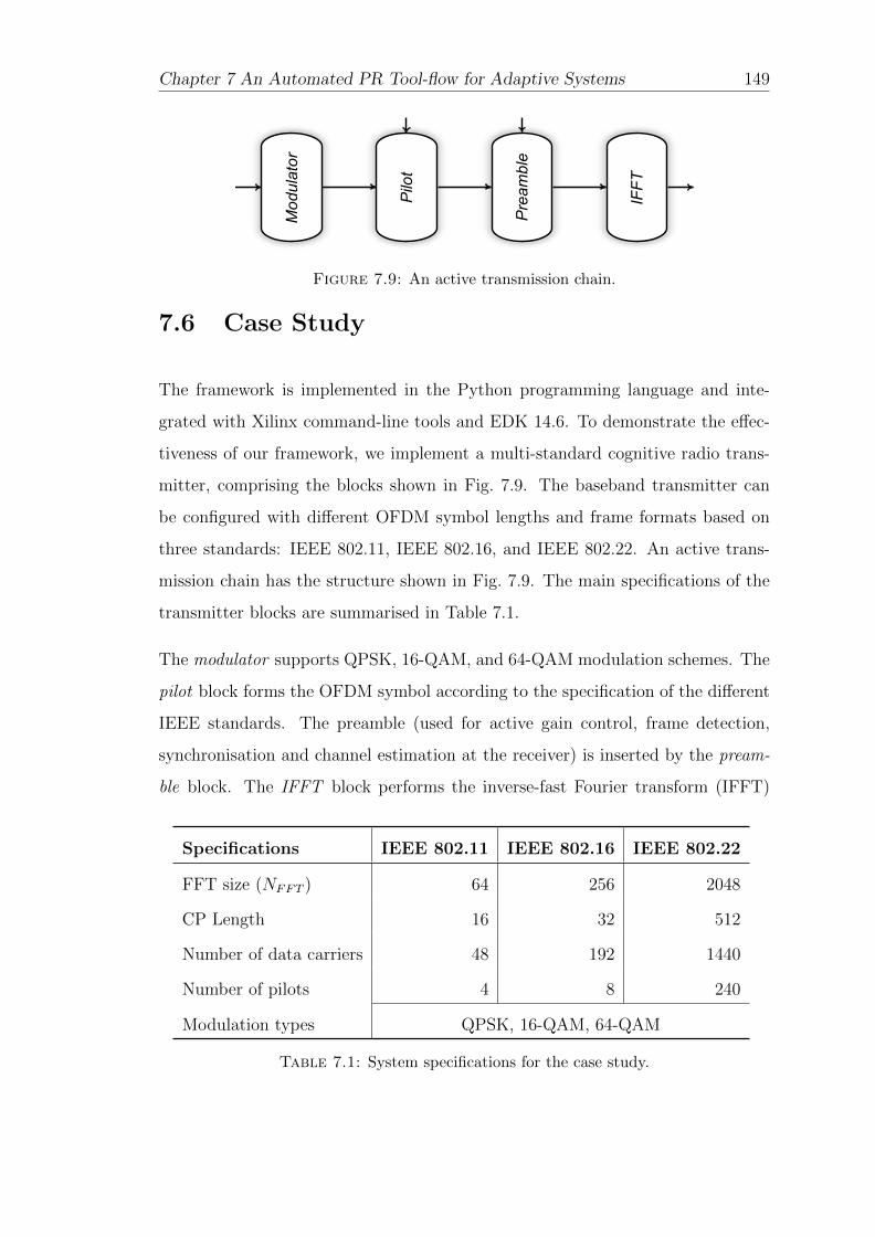
Chapter 7 An Automated PR Tool-flow for Adaptive Systems 149
Modulator
Pilot
Preamble
IFFT
Figure 7.9: An active transmission chain.
7.6 Case Study
The framework is implemented in the Python programming language and inte-
grated with Xilinx command-line tools and EDK 14.6. To demonstrate the effec-
tiveness of our framework, we implement a multi-standard cognitive radio trans-
mitter, comprising the blocks shown in Fig. 7.9. The baseband transmitter can
be configured with different OFDM symbol lengths and frame formats based on
three standards: IEEE 802.11, IEEE 802.16, and IEEE 802.22. An active trans-
mission chain has the structure shown in Fig. 7.9. The main specifications of the
transmitter blocks are summarised in Table 7.1.
The modulator supports QPSK, 16-QAM, and 64-QAM modulation schemes. The
pilot block forms the OFDM symbol according to the specification of the different
IEEE standards. The preamble (used for active gain control, frame detection,
synchronisation and channel estimation at the receiver) is inserted by the pream-
ble block. The IFFT block performs the inverse-fast Fourier transform (IFFT)
Specifications IEEE 802.11 IEEE 802.16 IEEE 802.22
FFT size (NFFT ) 64 256 2048
CP Length 16 32 512
Number of data carriers 48 192 1440
Number of pilots 4 8 240
Modulation types QPSK, 16-QAM, 64-QAM
Table 7.1: System specifications for the case study.
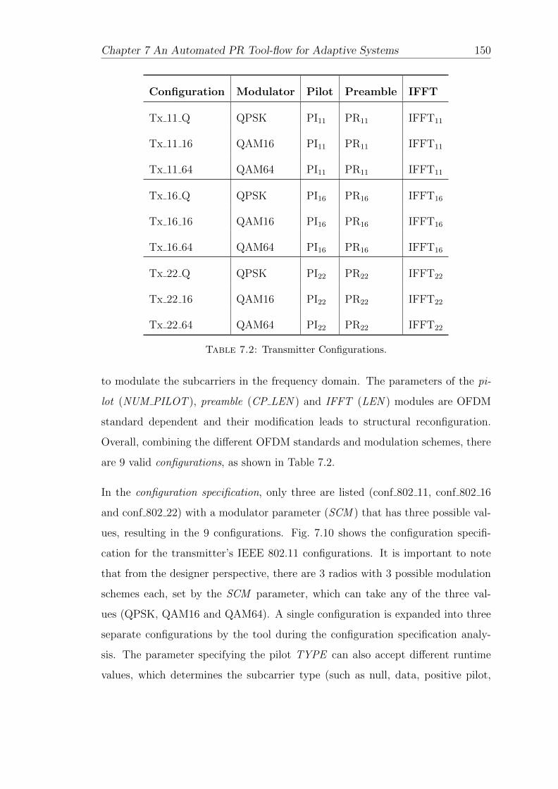
Chapter 7 An Automated PR Tool-flow for Adaptive Systems 150
Configuration Modulator Pilot Preamble IFFT
Tx 11 Q QPSK PI11 PR11 IFFT11
Tx 11 16 QAM16 PI11 PR11 IFFT11
Tx 11 64 QAM64 PI11 PR11 IFFT11
Tx 16 Q QPSK PI16 PR16 IFFT16
Tx 16 16 QAM16 PI16 PR16 IFFT16
Tx 16 64 QAM64 PI16 PR16 IFFT16
Tx 22 Q QPSK PI22 PR22 IFFT22
Tx 22 16 QAM16 PI22 PR22 IFFT22
Tx 22 64 QAM64 PI22 PR22 IFFT22
Table 7.2: Transmitter Configurations.
to modulate the subcarriers in the frequency domain. The parameters of the pi-
lot (NUM PILOT ), preamble (CP LEN ) and IFFT (LEN ) modules are OFDM
standard dependent and their modification leads to structural reconfiguration.
Overall, combining the different OFDM standards and modulation schemes, there
are 9 valid configurations, as shown in Table 7.2.
In the configuration specification, only three are listed (conf 802 11, conf 802 16
and conf 802 22) with a modulator parameter (SCM ) that has three possible val-
ues, resulting in the 9 configurations. Fig. 7.10 shows the configuration specifi-
cation for the transmitter’s IEEE 802.11 configurations. It is important to note
that from the designer perspective, there are 3 radios with 3 possible modulation
schemes each, set by the SCM parameter, which can take any of the three val-
ues (QPSK, QAM16 and QAM64). A single configuration is expanded into three
separate configurations by the tool during the configuration specification analy-
sis. The parameter specifying the pilot TYPE can also accept different runtime
values, which determines the subcarrier type (such as null, data, positive pilot,
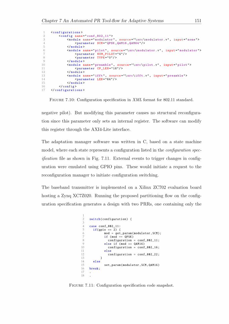
Chapter 7 An Automated PR Tool-flow for Adaptive Systems 151
1 <configurations >2 <config name=" conf_802_11">3 <module name=" modulator", source ="\src\modulator.v", input ="none">4 <parameter SCM="QPSK ,QAM16 ,QAM64"/>5 </module >6 <module name="pilot", source ="\src\modulator.v", input =" modulator">7 <parameter NUM_PILOT ="4"/>8 <parameter TYPE ="0"/>9 </module >
10 <module name=" preamble", source ="\src\pilot.v", input =" pilot">11 <parameter CP_LEN ="16"/ >12 </module >13 <module name="ifft", source ="\src\ifft.v", input=" preamble">14 <parameter LEN ="64"/ >15 </module >16 </config >17 </configurations >
Figure 7.10: Configuration specification in XML format for 802.11 standard.
negative pilot). But modifying this parameter causes no structural reconfigura-
tion since this parameter only sets an internal register. The software can modify
this register through the AXI4-Lite interface.
The adaptation manager software was written in C, based on a state machine
model, where each state represents a configuration listed in the configuration spec-
ification file as shown in Fig. 7.11. External events to trigger changes in config-
uration were emulated using GPIO pins. These would initiate a request to the
reconfiguration manager to initiate configuration switching.
The baseband transmitter is implemented on a Xilinx ZC702 evaluation board
hosting a Zynq XC7Z020. Running the proposed partitioning flow on the config-
uration specification generates a design with two PRRs, one containing only the
12 switch(configuration) {34 case conf_802_11:5 if(gpio == 2) {6 mod = get_param(modulator ,SCM);7 if (mod == QPSK)8 configuration = conf_802_11;9 else if (mod == QAM16)
10 configuration = conf_802_16;11 else12 configuration = conf_802_22;13 }14 else15 set_param(modulator ,SCM,QAM16)16 break;17 .18 .
Figure 7.11: Configuration specification code snapshot.
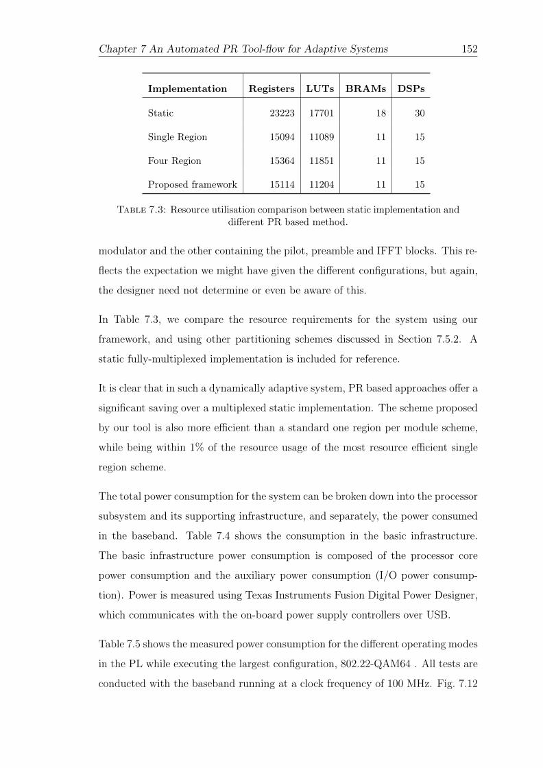
Chapter 7 An Automated PR Tool-flow for Adaptive Systems 152
Implementation Registers LUTs BRAMs DSPs
Static 23223 17701 18 30
Single Region 15094 11089 11 15
Four Region 15364 11851 11 15
Proposed framework 15114 11204 11 15
Table 7.3: Resource utilisation comparison between static implementation anddifferent PR based method.
modulator and the other containing the pilot, preamble and IFFT blocks. This re-
flects the expectation we might have given the different configurations, but again,
the designer need not determine or even be aware of this.
In Table 7.3, we compare the resource requirements for the system using our
framework, and using other partitioning schemes discussed in Section 7.5.2. A
static fully-multiplexed implementation is included for reference.
It is clear that in such a dynamically adaptive system, PR based approaches offer a
significant saving over a multiplexed static implementation. The scheme proposed
by our tool is also more efficient than a standard one region per module scheme,
while being within 1% of the resource usage of the most resource efficient single
region scheme.
The total power consumption for the system can be broken down into the processor
subsystem and its supporting infrastructure, and separately, the power consumed
in the baseband. Table 7.4 shows the consumption in the basic infrastructure.
The basic infrastructure power consumption is composed of the processor core
power consumption and the auxiliary power consumption (I/O power consump-
tion). Power is measured using Texas Instruments Fusion Digital Power Designer,
which communicates with the on-board power supply controllers over USB.
Table 7.5 shows the measured power consumption for the different operating modes
in the PL while executing the largest configuration, 802.22-QAM64 . All tests are
conducted with the baseband running at a clock frequency of 100 MHz. Fig. 7.12
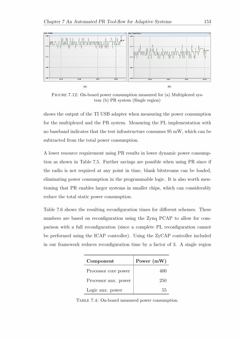
Chapter 7 An Automated PR Tool-flow for Adaptive Systems 153
(a) (b)
Figure 7.12: On-board power consumption measured for (a) Multiplexed sys-tem (b) PR system (Single region)
shows the output of the TI USB adapter when measuring the power consumption
for the multiplexed and the PR system. Measuring the PL implementation with
no baseband indicates that the test infrastructure consumes 95 mW, which can be
subtracted from the total power consumption.
A lower resource requirement using PR results in lower dynamic power consump-
tion as shown in Table 7.5. Further savings are possible when using PR since if
the radio is not required at any point in time, blank bitstreams can be loaded,
eliminating power consumption in the programmable logic. It is also worth men-
tioning that PR enables larger systems in smaller chips, which can considerably
reduce the total static power consumption.
Table 7.6 shows the resulting reconfiguration times for different schemes. These
numbers are based on reconfiguration using the Zynq PCAP to allow for com-
parison with a full reconfiguration (since a complete PL reconfiguration cannot
be performed using the ICAP controller). Using the ZyCAP controller included
in our framework reduces reconfiguration time by a factor of 3. A single region
Component Power (mW)
Processor core power 400
Processor aux. power 250
Logic aux. power 55
Table 7.4: On-board measured power consumption.

Chapter 7 An Automated PR Tool-flow for Adaptive Systems 154
Style Power (mW)
Static 79
Single Region 33
Four Regions 54
Proposed PR method 43
PR with blank bitstream 0
Table 7.5: Dynamic power consumption in the baseband for different schemes.
scheme requires the whole region to be reconfigured any time one module is recon-
figured. Since the total resource requirement for the four region scheme is higher,
the total reconfiguration time is higher than the arrangement determined by the
Scheme Bitstream (Bytes) Reconf. time (ms)
Full reconfiguration 4045564 31.12
Single Region 706192 5.18
Four Regions
Region-1 14544 0.11
Region-2 14544 0.11
Region-3 677104 5.12
Region-4 14544 0.11
Total 720736 5.45
Proposed PR method
Region-1 14544 0.11
Region-2 691648 5.07
Total 706192 5.18
Table 7.6: Reconfiguration time for PR and non-PR based methods.

Chapter 7 An Automated PR Tool-flow for Adaptive Systems 155
framework when the transmitter switches from one OFDM standard to another.
Another benefit of the proposed partitioning is that switching only the modulation
scheme can be done in minimal time as the modulator is implemented in its own
region.
The framework enables radio developers to try different adaptation algorithms for
efficient spectrum usage without worrying about implementation or reconfigura-
tion details. This enables faster system prototyping and lower engineering effort,
thus improving design productivity. As is clear, the low-level details are consid-
ered and optimised by the framework, but abstracted from the designer’s point of
view.
7.7 Summary
This chapter has introduced an automated framework for the design of dynamically
adaptive systems using partial reconfiguration. It takes a high-level description of
an adaptive system, automatically partitions the design into reconfigurable regions
and determines a floorplan. Runtime adaptation control is also automatically
generated, isolating the designer from the low-level aspects of the implementation.
We have shown an example application to demonstrate the effectiveness of the
proposed framework. Our framework is also suitable for integration with other
high-level PR tools such as those deriving partitions from task-graphs, allowing
for easy validation of results on real hardware.
The framework, named CoPR, has been released in the public domain, so it can
be used by researchers intending to incorporate PR into their systems.
Chapter 8
An Open source Development
and Testbed for PR Systems
8.1 Introduction
In previous chapters, we discussed how PR can enable the implementation of adap-
tive systems on FPGA platforms. One major challenge faced by PR based system
developers generally is hardware validation. In Chapter 7, we discussed the im-
plementation strategy for PR based systems in an embedded environment using
hybrid FPGAs. But often, FPGAs are used as sub-systems tethered to a host
machine with the data plane implemented on the FPGA and the control plane im-
plemented using an general purpose processor in a host PC. This is especially true
for non-hybrid FPGA platforms, which do not contain a fully-fledged processor.
For these systems, the communication and reconfiguration costs are much higher
as they are carried out through standard communication interfaces. Integrating
FPGAs within general purpose computers also allows PR to be leveraged for im-
plementing accelerators within larger software systems, as well as easing system
testing and verification, with the host offering a software view of the hardware
resource.
156
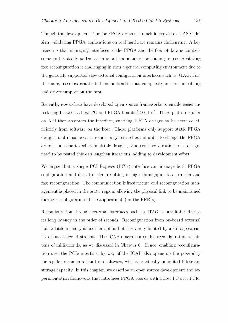
Chapter 8 An Open source Development and Testbed for PR Systems 157
Though the development time for FPGA designs is much improved over ASIC de-
sign, validating FPGA applications on real hardware remains challenging. A key
reason is that managing interfaces to the FPGA and the flow of data is cumber-
some and typically addressed in an ad-hoc manner, precluding re-use. Achieving
fast reconfiguration is challenging in such a general computing environment due to
the generally supported slow external configuration interfaces such as JTAG. Fur-
thermore, use of external interfaces adds additional complexity in terms of cabling
and driver support on the host.
Recently, researchers have developed open source frameworks to enable easier in-
terfacing between a host PC and FPGA boards [150, 151]. These platforms offer
an API that abstracts the interface, enabling FPGA designs to be accessed ef-
ficiently from software on the host. These platforms only support static FPGA
designs, and in some cases require a system reboot in order to change the FPGA
design. In scenarios where multiple designs, or alternative variations of a design,
need to be tested this can lengthen iterations, adding to development effort.
We argue that a single PCI Express (PCIe) interface can manage both FPGA
configuration and data transfer, resulting in high throughput data transfer and
fast reconfiguration. The communication infrastructure and reconfiguration man-
agement is placed in the static region, allowing the physical link to be maintained
during reconfiguration of the application(s) in the PRR(s).
Reconfiguration through external interfaces such as JTAG is unsuitable due to
its long latency in the order of seconds. Reconfiguration from on-board external
non-volatile memory is another option but is severely limited by a storage capac-
ity of just a few bitstreams. The ICAP macro can enable reconfiguration within
tens of milliseconds, as we discussed in Chapter 6. Hence, enabling reconfigura-
tion over the PCIe interface, by way of the ICAP also opens up the possibility
for regular reconfiguration from software, with a practically unlimited bitstream
storage capacity. In this chapter, we describe an open source development and ex-
perimentation framework that interfaces FPGA boards with a host PC over PCIe,
Chapter 8 An Open source Development and Testbed for PR Systems 158
using PR to manage reconfiguration. This frameworkd can serve as a verifica-
tion platform for PR based designs, or as a platform for integrating reconfigurable
accelerators in large software systems.
The work presented in this chapter has also been discussed in:
• K. Vipin, S. Shreejith, D. Gunasekara, S. A. Fahmy, and N. Kapre, System-
Level FPGA Device Driver with High-Level Synthesis Support, in Proceed-
ings of the International Conference on Field Programmable Technology
(FPT) , Kyoto, Japan, December 2013, pp. 128-135. [152].
• K. Vipin and S. A. Fahmy, DyRACT: A Partial Reconfiguration Enabled Ac-
celerator and Test Platform, in Proceedings of the International Conference
on Field Programmable Logic and Applications (FPL), Munich, Germany,
September 2014. [153].
8.2 Related Work
Numerous approaches to interfacing FPGAs with host PCs have been proposed.
A PCI-X based interface was described in [154] achieving a throughput of up to
667 MB/s. SIRC [150] is another framework for interfacing a Windows host PC and
an FPGA board over Ethernet. However, Ethernet fails to offer the throughput
capabilities often required for such software-hardware systems. Recently, frame-
works that interface over higher throughput PCI Express (PCIe) links, such as
RIFFA [151, 155] and OCPI [156], have emerged. These frameworks enable static
FPGA designs to be accessed through an abstracted software API on the host, in-
cluding hooks for different programming languages. However, in some cases, these
frameworks require a host reboot when the FPGA application is reconfigured, or
they rely on PCIe features that can be unreliable to support hot-reconfiguration.
Furthermore, loading new user logic requires complete re-implementation of the
full design, including fixed communication infrastructure. This can lead to issues
with timing closure for large designs, and consumes considerable time. Hence, the

Chapter 8 An Open source Development and Testbed for PR Systems 159
use of these frameworks in the context of dynamically reconfigurable accelerators
is not possible.
For designers who build partially reconfigurable systems, testing remains an issue.
A functional approach was proposed in [157], however a real hardware test using
bitstreams requires considerable effort in implementing the full communication
and reconfiguration architecture, and this is often done in an ad-hoc manner.
While reconfiguration time may not be an essential factor to consider in a testing
platform, minimising it would allow this framework to be used as a platform for
reconfigurable hardware accelerators in general purpose PCs. If not managed
efficiently, reconfiguration can consume a considerable amount of overall system
execution time in software-hardware systems [158, 159]. While PR is supported
through the JTAG interface, internal controllers such as the ICAP offer much
better performance, as they provide direct access to the configuration memory
from the FPGA fabric. Some have even suggested alternative external interfaces
like RS-232, though the achievable throughput is clearly limited [160]. Vendor-
provided ICAP controllers offer poor throughput as we saw in Chapter 6, though
the ICAP interface itself is capable of much higher throughput.
For this framework, we propose to load partial bitstreams over the PCIe interface
that is also used for data communication. This has been demonstrated by Xilinx,
but with a low reconfiguration speed of 30 MB/s and supporting only a one-time
reconfiguration [161]. This approach was improved in [162], enabling multiple
reconfigurations, but the reconfiguration speed remained low due to the lack of
DMA support.
8.3 Contributions
We present a framework incorporating a hardware design and associated software
interface for loading PR based designs into an FPGA over a static PCIe interface,
then allowing high throughput communication between the host and hardware
Chapter 8 An Open source Development and Testbed for PR Systems 160
XilinxSPCIeSEndpointS
Mx4SGen.2O
ReceiveSEngine
TransmitSEngine
GlobalSRegisterSSet
PSG-4
PSA
PSG-1
PSG-2Config.
Controller
UserSLogic
Use
rSLo
gic
SAda
pter
ClockSMgmt
ControlSLogic
PIOSInterface
Strm-1SI/F
Strm-2SI/F
Strm-4SI/F
Figure 8.1: Framework hardware architecture.
design. Reconfiguration and data throughput are shown to be close the the theo-
retical maximum supported by the PCIe interface. This framework is of interest for
adaptive system development, as it enables hardware validation of the dataplane
and verification of the reconfiguration management software. It also facilitates
the implementation of loosely-coupled adaptive systems with a PC host, and the
integration of reconfigurable accelerators within larger software programs running
on a host PC.
8.4 Hardware-Software Architecture
The hardware framework is comprised of the control logic and user logic, as shown
in Fig. 8.1. The control logic implements interface management, reconfiguration
control, and clock management, while the user logic implements the design under
test (DUT) such as the adaptive system dataplane. The control logic is imple-
mented in the static region, while the user logic is implemented using one or more
partially reconfigurable regions (PRR), which can be reconfigured at runtime over
PCIe. The framework is interfaced with a host machine such as a PC or a work-
station through the PCIe interface. The software to manage the framework, such
Chapter 8 An Open source Development and Testbed for PR Systems 161
as the reconfiguration manager, runs on the host processor. The following sections
describe each block of the platform in detail.
8.4.1 PCIe Endpoint Block
The PCIe bus standard follows a layered communication architecture with physi-
cal, data link, and transaction layers. The physical layer manages low level electri-
cal and logical operations whereas the data link layer implements flow control and
interface reliability. We use the Xilinx PCIe Integrated Endpoint Block, configured
for PCIe Gen 2 ×4 link width to implement the physical and data link layers.
Theoretically this gives a maximum throughput of 2 GB/s per direction in full-
duplex mode, and this is portable across all Virtex-6 and Virtex-7 FPGAs. Newer
boards can support higher bandwidths, which can be exploited with some rework-
ing of our interface. The backend of the PCIe block is a 64-bit wide AXI4-Stream
interface clocked at 250 MHz.
The maximum payload size (MPS) for the PCIe block is set to 256 Bytes and the
block uses 4 BRAM based buffers to store the PCIe packets. PCIe defines the MPS
as the maximum packet size allowed for an endpoint. When an endpoint generates
packets, the packet size should not exceed this size and the packets received by the
endpoint will always be less than or equal to this size. The endpoint can request
an MPS between 128 to 4096 Bytes and this is set by the host during PCIe
initialisation. Keeping the MPS size smaller reduces the achievable throughput
due to the packet overhead, but it reduces the buffering requirement and makes
the implementation portable across multiple host machines. The maximum read
request size (MRRS) for the endpoint when it makes memory read requests is set
to 4096 Bytes for better read performance.
Chapter 8 An Open source Development and Testbed for PR Systems 162
8.4.2 PCIe Transaction Layer
The Endpoint block is directly interfaced with the receive and transmit engines,
which together act as the PCIe transaction layer. Here, transaction layer pack-
ets (TLPs) are generated and consumed, representing the unit of communication
for PCIe. TLPs follow a specific packet format as outlined in the PCIe specifi-
cation [163]. Each TLP has a header field specifying the type of packet such as
memory read, memory write, or read completion. Memory read and write packets
are used to initiate a read or write operation respectively, and a completion packet
contains the result of a read operation. The receive engine decodes received TLPs
and routes them to the appropriate target. If the memory request is for an address
location below 0x400, it is routed to the global register set, otherwise it is directed
to the user address/data interface. The transmit engine generates memory read
TLPs during the DMA operation to fetch data from host memory, memory write
TLPs to transmit data from the FPGA to host memory, and completion TLPs in
response to read requests from the host.
8.4.3 Global Register Set
This module implements all the control and status registers required for interface,
communication and configuration management. An overview of important regis-
ters implemented and their address map is given in Table 8.1. The control register
is used to initiate DMA operations between the host and FPGA, as well as to
trigger reconfiguration operations. The status register is updated after each DMA
or reconfiguration operation, allowing the host to ascertain operation completion.
The user control register implements bits for selectively resetting the user logic as
well as to select the clock frequency for the user stream interface. To initiate a
reconfiguration operation, the host sets the bitstream size and its starting location
in the host memory in the CONF LEN and CONF ADDR registers before setting
the control register bit. Separate address and length registers are used to enable
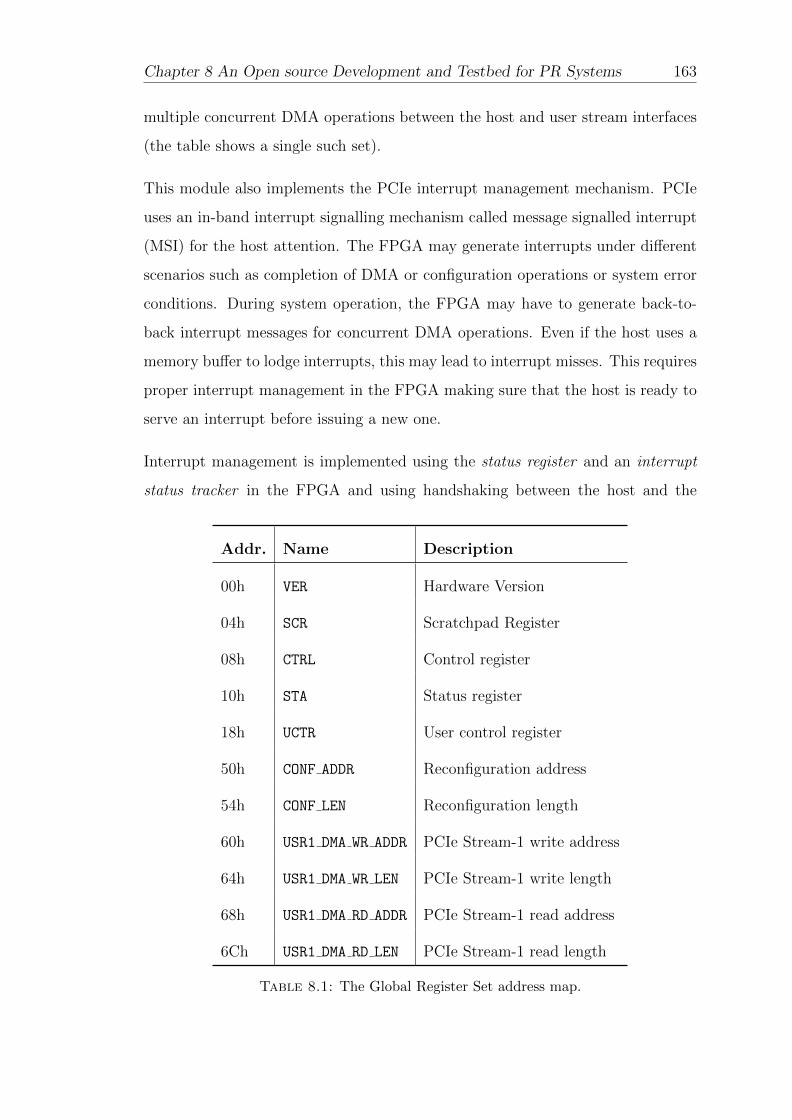
Chapter 8 An Open source Development and Testbed for PR Systems 163
multiple concurrent DMA operations between the host and user stream interfaces
(the table shows a single such set).
This module also implements the PCIe interrupt management mechanism. PCIe
uses an in-band interrupt signalling mechanism called message signalled interrupt
(MSI) for the host attention. The FPGA may generate interrupts under different
scenarios such as completion of DMA or configuration operations or system error
conditions. During system operation, the FPGA may have to generate back-to-
back interrupt messages for concurrent DMA operations. Even if the host uses a
memory buffer to lodge interrupts, this may lead to interrupt misses. This requires
proper interrupt management in the FPGA making sure that the host is ready to
serve an interrupt before issuing a new one.
Interrupt management is implemented using the status register and an interrupt
status tracker in the FPGA and using handshaking between the host and the
Addr. Name Description
00h VER Hardware Version
04h SCR Scratchpad Register
08h CTRL Control register
10h STA Status register
18h UCTR User control register
50h CONF ADDR Reconfiguration address
54h CONF LEN Reconfiguration length
60h USR1 DMA WR ADDR PCIe Stream-1 write address
64h USR1 DMA WR LEN PCIe Stream-1 write length
68h USR1 DMA RD ADDR PCIe Stream-1 read address
6Ch USR1 DMA RD LEN PCIe Stream-1 read length
Table 8.1: The Global Register Set address map.
Chapter 8 An Open source Development and Testbed for PR Systems 164
FPGA. When the FPGA issues an interrupt, a corresponding bit is set in the
status register. There are separate bits in the status register indicating different
interrupt conditions. The interrupt tracker continuously checks for any bit set in
the status register (the register is wired-or), and when it finds a condition, issues
an interrupt to the host. The tracker then waits for the host to acknowledge the
interrupt before checking the status register again, meanwhile the status register
may lodge more interrupts. The host acknowledges an interrupt by reading the
status register and write-clearing only the bits it finds already set. In this way, a
single interrupt can convey multiple conditions and the tracker makes sure that
the host is ready to accept interrupt before issuing a new one.
8.4.4 PCIe Stream Generator (PSG)
The PCIe Stream Generators (PSG) act as the DMA controllers between the host
and user stream interfaces. Modern processor chipsets do not have DMA con-
trollers between the host memory and downstream PCIe devices. This requires
the DMA controllers to be implemented in the FPGA fabric. Our framework sup-
ports a configurable number of PSGs, with each one managing a single user stream
interface. The present implementation supports up to 4 concurrent streaming in-
terfaces to user logic.
Since a single read request cannot be larger than 4KB (as per the PCIe protocol), a
PSG has to make multiple read requests to the host during DMA write operations
(from host to FPGA). When an endpoint device makes multiple outstanding read
requests, the completion packets may return out of order. Typically, the endpoint
is forced to make a new request only after receiving the data for the previous
request. This can severely degrade performance since there can be a large latency
between a memory read request and its completion. To achieve full bandwidth
during DMA write operations, the FPGA must be able to issue back to back read
requests to the host while managing out of order completions.

Chapter 8 An Open source Development and Testbed for PR Systems 165
FIFO-1s(tag-1)
FIFO-2s(tag-2)FIFO-Ns(tag-N)
Empty
fifo1_rcv_len_reg
fifo1_req_len_reg
Readsrequests
generator
Read_req
Read_len
Read_tagTagdecoder
Data_in Tag_in
Wr_en
Data_in
Sequencer
Data_out
Rd_enData_out
DMA_req DMA_done
Figure 8.2: PSG DMA read manager
We exploit the tag number field in the PCIe packet headers to implement virtual
channels, which enable multiple outbound read requests. Tag management is
implemented with the help of FIFOs and a set of associated control registers as
shown in Fig. 8.2. The number of FIFOs used is equal to the number of virtual
channels and each virtual channel uses a unique tag number. The FIFO depth
is fixed to 4KB, so that it can store the complete data resulting from a single
read request. A read request generates multiple outbound read requests up to the
number of virtual channels. When packets are received in response to the read
requests, logic checks the tag number and routes the data to the appropriate FIFO.
Later a read sequencer is used to reorder the data by reading sequentially from
the FIFOs. Our experiments show that implementing only two virtual channels
provides sufficiently high throughput performance (75% of PCIe bandwidth) for
PCIe Gen 2 x4.
8.4.5 PCIe Stream Arbitrator (PSA)
Arbitration logic is required to fairly serve the requests from multiple PSGs ac-
cessing the transaction layer. Our present design is scalable, supporting up to 256
stream interfaces with round-robin arbitration among them. In order to achieve
Chapter 8 An Open source Development and Testbed for PR Systems 166
high performance, a PSG is granted bus access until no other PSG makes a re-
quest. This avoids unnecessary cycle loss present in traditional fixed time slot
based round-robin-arbitration.
8.4.6 Configuration Controller
The configuration controller is a key feature of this framework. It manages partial
reconfiguration of the user logic. We adapt our custom ICAP controller presented
in Chapter 6 to implement this. Instead of reading partial bitstreams from external
DDR memory, the modified implementation receives partial bitstreams directly
from the host machine over the PCIe bus and configures the PRRs.
Two independent state machines, the configuration state machine (CSM) and the
ICAP state machine (ISM), manage low-level reconfiguration. The configuration
operation is triggered by the control register after the host configures the partial
bitstream size and its location in the host memory in the global register set. The
CSM generates memory read requests to the host to receive the partial bitstream.
Received bitstream data is stored in an 8KB asynchronous asymmetric FIFO, with
a 64-bit write port clocked at 250 MHz. The CSM generates a new read request
only when all data corresponding to the previous request is received and there is
sufficient space in the FIFO. Unlike PSGs, the configuration controller does not
implement virtual channels since the maximum reconfiguration speed supported
by the ICAP is only 400 MB/s and they are not needed.
The ICAP state machine (ISM) constantly monitors the read port of the FIFO
for bitstream data. The FIFO read port is 32 bits wide clocked at 100 MHz – the
maximum clock frequency supported by the ICAP. As soon as the FIFO empty
signal is de-asserted, the ISM fetches data from the FIFO and writes it to the
ICAP. Since the FIFO depth is double the maximum PCIe read request size, the
bitstream read from host memory can overlap with ICAP transactions, maximising
reconfiguration throughput.
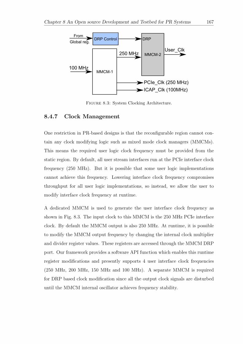
Chapter 8 An Open source Development and Testbed for PR Systems 167
100aMHz
User_Clk250aMHz
PCIe_Clka(250aMHz)
ICAP_Clka(100MHz)
MMCM-1
MMCM-2
DRPDRPaControlFrom
Globalareg.
Figure 8.3: System Clocking Architecture.
8.4.7 Clock Management
One restriction in PR-based designs is that the reconfigurable region cannot con-
tain any clock modifying logic such as mixed mode clock managers (MMCMs).
This means the required user logic clock frequency must be provided from the
static region. By default, all user stream interfaces run at the PCIe interface clock
frequency (250 MHz). But it is possible that some user logic implementations
cannot achieve this frequency. Lowering interface clock frequency compromises
throughput for all user logic implementations, so instead, we allow the user to
modify interface clock frequency at runtime.
A dedicated MMCM is used to generate the user interface clock frequency as
shown in Fig. 8.3. The input clock to this MMCM is the 250 MHz PCIe interface
clock. By default the MMCM output is also 250 MHz. At runtime, it is possible
to modify the MMCM output frequency by changing the internal clock multiplier
and divider register values. These registers are accessed through the MMCM DRP
port. Our framework provides a software API function which enables this runtime
register modifications and presently supports 4 user interface clock frequencies
(250 MHz, 200 MHz, 150 MHz and 100 MHz). A separate MMCM is required
for DRP based clock modification since all the output clock signals are disturbed
until the MMCM internal oscillator achieves frequency stability.
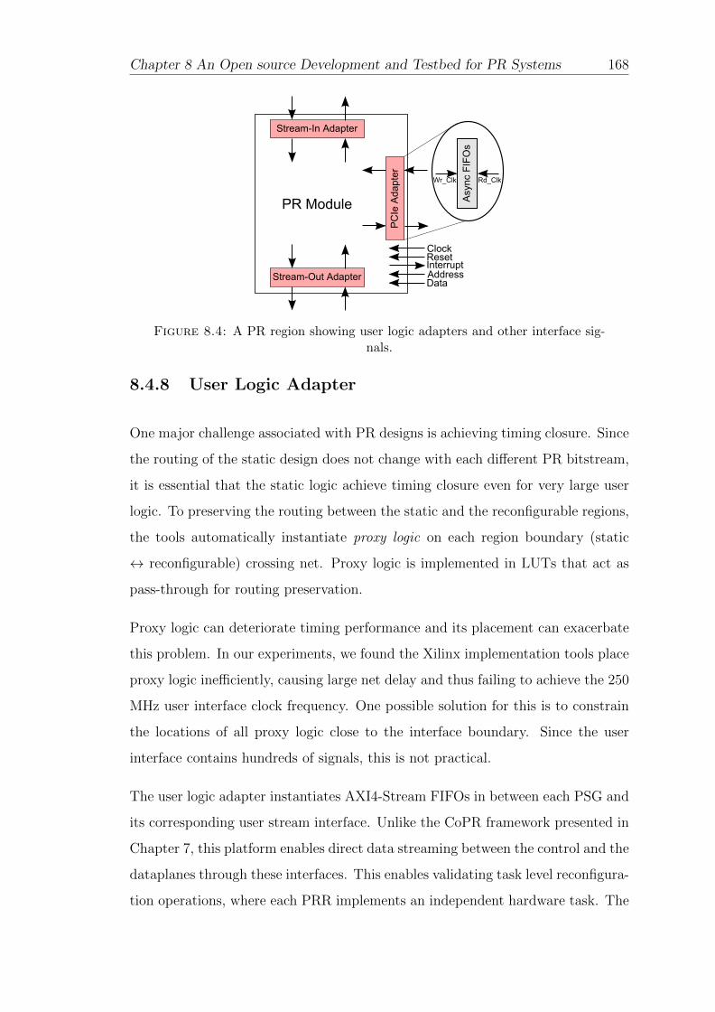
Chapter 8 An Open source Development and Testbed for PR Systems 168
PC
Ie A
dapt
er
Stream-In Adapter
Stream-Out Adapter
ClockResetInterruptAddressData
Asy
nc F
IFO
s
Wr_Clk Rd_Clk
PR Module
Figure 8.4: A PR region showing user logic adapters and other interface sig-nals.
8.4.8 User Logic Adapter
One major challenge associated with PR designs is achieving timing closure. Since
the routing of the static design does not change with each different PR bitstream,
it is essential that the static logic achieve timing closure even for very large user
logic. To preserving the routing between the static and the reconfigurable regions,
the tools automatically instantiate proxy logic on each region boundary (static
↔ reconfigurable) crossing net. Proxy logic is implemented in LUTs that act as
pass-through for routing preservation.
Proxy logic can deteriorate timing performance and its placement can exacerbate
this problem. In our experiments, we found the Xilinx implementation tools place
proxy logic inefficiently, causing large net delay and thus failing to achieve the 250
MHz user interface clock frequency. One possible solution for this is to constrain
the locations of all proxy logic close to the interface boundary. Since the user
interface contains hundreds of signals, this is not practical.
The user logic adapter instantiates AXI4-Stream FIFOs in between each PSG and
its corresponding user stream interface. Unlike the CoPR framework presented in
Chapter 7, this platform enables direct data streaming between the control and the
dataplanes through these interfaces. This enables validating task level reconfigura-
tion operations, where each PRR implements an independent hardware task. The

Chapter 8 An Open source Development and Testbed for PR Systems 169
Stream FIFOs reside in the reconfigurable region and their locations are manually
constrained close to the region boundary. This causes the implementation tools
to place the proxy logic close to the interface boundary and thus help with timing
closure. This adapter is automatically added to the design by our development
infrastructure and users do not have to consider it when designing their user logic.
In addition to the PCIe stream interface, each PRR has two other stream interfaces
to connect with adjacent PRRs, enabling module chaining to implement different
processing chains as shown in Fig. 8.4. This is similar to the AXI4-Stream in-
terface connecting different PRRs in the CoPR framework enabling direct data
streaming between multiple hardware modules to form different system configura-
tions. Similar to the AXI-Lite interface present in the CoPR platform, each PRR
also has an address/data interface, which enables parametric reconfiguration of
the modules implemented in them.
The user logic adapter also performs clock domain crossing management. The
FIFOs used in the adapter are asynchronous in nature with their PSG side port
operating at the PCIe interface frequency (250 MHz). The FIFO ports interfaced
with the user logic interface run at the configurable user logic clock (100MHz to
250MHz). This provides reliable clock domain crossing between the control logic
and the user logic.
8.4.9 Software Infrastructure
The software component of our framework consists of a PCIe driver and a user
library supported on Linux. The low level PCIe driver is an extensively modified
version of the RIFFA driver with the user library providing API functions listed in
Table 8.2. The fpga send data() and fpga recv data() functions are used for DMA
transfer between the host and user stream interfaces. The specific user stream
interface number is provided as an argument to these APIs. The fpga reconfig()
function is used to initiate a reconfiguration operation by specifying the partial
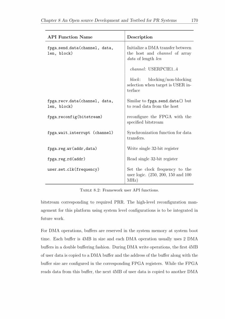
Chapter 8 An Open source Development and Testbed for PR Systems 170
API Function Name Description
fpga send data(channel, data,
len, block)
Initialize a DMA transfer betweenthe host and channel of arraydata of length len
channel : USERPCIE1..4
block : blocking/non-blockingselection when target is USER in-terface
fpga recv data(channel, data,
len, block)
Similar to fpga send data() butto read data from the host
fpga reconfig(bitstream) reconfigure the FPGA with thespecified bitstream
fpga wait interrupt (channel) Synchronization function for datatransfers.
fpga reg wr(addr,data) Write single 32-bit register
fpga reg rd(addr) Read single 32-bit register
user set clk(frequency) Set the clock frequency to theuser logic. (250, 200, 150 and 100MHz)
Table 8.2: Framework user API functions.
bitstream corresponding to required PRR. The high-level reconfiguration man-
agement for this platform using system level configurations is to be integrated in
future work.
For DMA operations, buffers are reserved in the system memory at system boot
time. Each buffer is 4MB in size and each DMA operation usually uses 2 DMA
buffers in a double buffering fashion. During DMA write operations, the first 4MB
of user data is copied to a DMA buffer and the address of the buffer along with the
buffer size are configured in the corresponding FPGA registers. While the FPGA
reads data from this buffer, the next 4MB of user data is copied to another DMA
Chapter 8 An Open source Development and Testbed for PR Systems 171
buffer. When the FPGA indicates the completion of the data transfer correspond-
ing to the first DMA buffer through an interrupt, the information corresponding
to the second buffer is configured in the FPGA. The first buffer is now free for
copying more user data. This cycle continues until the complete user data is sent
to the FPGA.
For DMA read operations, a similar double-buffering based scheme is used. In
this case DMA buffers are used to store data received from the FPGA and data
reception overlaps with copying data to the user provided buffer from the DMA
buffers.
The send and receive operations can act in both blocking and non-blocking modes.
In blocking mode, the API call returns only after the DMA operation is complete
while in non-blocking mode the API returns immediately after initiating a trans-
fer. Non-blocking operations are supported only for data transfers below 4 MB,
since data transfers above this size require two buffers and interrupt based buffer
management. Non-blocking mode transfer enables overlapping DMA operations to
multiple stream interfaces and overlapped read-write operations providing better
throughput for small data transfers. Non-blocking transfers must be synchronised
with the fpga wait interrupt() function before starting a new DMA operation to
the same channel.
8.5 Implementation and Characterisation
In this section we discuss the implementation details of the platform on multiple
target FPGAs. Detailed communication and reconfiguration performance numbers
are reported. We also present an example application built using the proposed
platform to demonstrate its functionality.
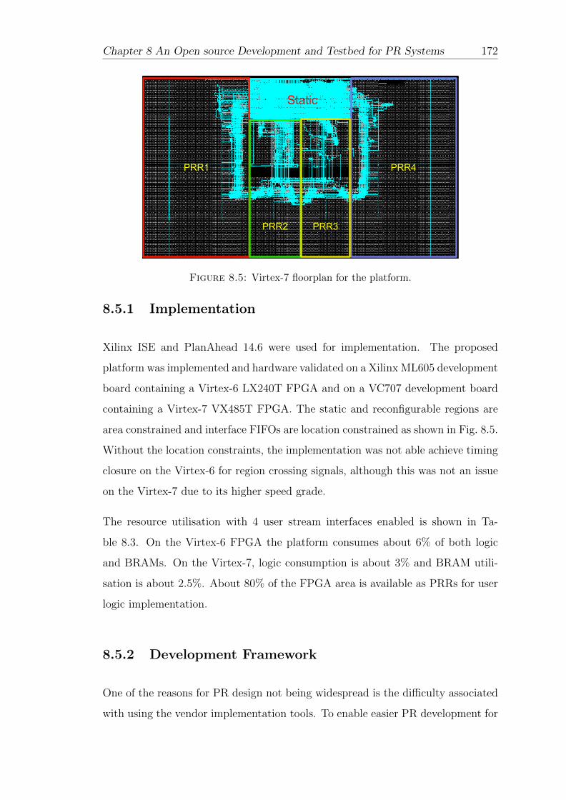
Chapter 8 An Open source Development and Testbed for PR Systems 172
PRR1 PRR4
PRR2 PRR3
Static
Figure 8.5: Virtex-7 floorplan for the platform.
8.5.1 Implementation
Xilinx ISE and PlanAhead 14.6 were used for implementation. The proposed
platform was implemented and hardware validated on a Xilinx ML605 development
board containing a Virtex-6 LX240T FPGA and on a VC707 development board
containing a Virtex-7 VX485T FPGA. The static and reconfigurable regions are
area constrained and interface FIFOs are location constrained as shown in Fig. 8.5.
Without the location constraints, the implementation was not able achieve timing
closure on the Virtex-6 for region crossing signals, although this was not an issue
on the Virtex-7 due to its higher speed grade.
The resource utilisation with 4 user stream interfaces enabled is shown in Ta-
ble 8.3. On the Virtex-6 FPGA the platform consumes about 6% of both logic
and BRAMs. On the Virtex-7, logic consumption is about 3% and BRAM utili-
sation is about 2.5%. About 80% of the FPGA area is available as PRRs for user
logic implementation.
8.5.2 Development Framework
One of the reasons for PR design not being widespread is the difficulty associated
with using the vendor implementation tools. To enable easier PR development for

Chapter 8 An Open source Development and Testbed for PR Systems 173
HardwareSpecification
ImplementationscriptDatabase
VendorEtoolchain
SpecifyEboardandEPRR
WriteEhigh-levelSoftware
gccECompiler
SystemEExecution
FPGAELibrary
Figure 8.6: Development Flow for the Testbed.
the proposed test platform, we provide a development environment in the form
of PR automation scripts. The proposed development platform is depicted in
Fig. 8.6. The designer only has to develop the reconfigurable modules conforming
to the predefined user logic interface. The designer then runs the implementa-
tion scripts by specifying the target FPGA board and the reconfigurable region.
The scripts use a database containing pre-synthesised netlists, placed and routed
control logic and implementation constraints for the framework, automatically in-
corporating the specific user logic into the design, and generating the full and
FPGA Virtex-6 LX240T Virtex-7 VX485T
Module Regs LUTs BRAMs Regs LUTs BRAMs
PCIe Core 791 738 4 1402 923 4
Transaction layer 1058 727 0 1069 613 0
DMA Control 2711 2809 12 2564 2519 12
Config. Control 451 328 2 298 261 2
Clock management 85 84 0 85 73 0
User Adapter 1556 791 8 1556 792 8
Total 6652 5477 26 6974 5181 26
Table 8.3: Platform Resouce utilisation
Chapter 8 An Open source Development and Testbed for PR Systems 174
partial bitstreams. This provides several advantages:
1. The pre-routed control logic has already achieved timing closure using spe-
cific location constraints.
2. Designers are not required to do manual floorplanning.
3. Using pre-routed control logic considerably reduces overall tool execution
time.
4. Since the specific IP-cores are already routed, issues related to software ver-
sion differences are avoided.
If designers are interested in additional exploration of the platform, they are free
to do so by completely reimplementing the control logic using the corresponding
HDL design files and modifying the user constraints file (UCF).
The designer writes the high-level software using the software APIs provided by
the framework. The provided reconfiguration API function (fpga reconfig()) can
be used in user C code to reconfigure the FPGA with the specified user partial
bitsreams, as generated by the scripts. This allows rapid and easy iteration for
testing multiple designs/variations. The framework also makes it possible to inte-
grate a hardware accelerator within a larger software application, by configuring
an accelerator and sending data at high throughput. The software is compiled
using the standard C compiler to generate the software executable.
For hardware validation, a full bitstream is stored in on-board flash memory to
configure the FPGA at system boot time – this contains the full static system and
empty PRRs. At runtime modules can be dynamically swapped in and out using
the API functions. Designers can also explore additional features such as module
chaining by configuring multiple PRRs concurrently and module pre-fetching by
reconfiguring regions when data is being processed in other regions.
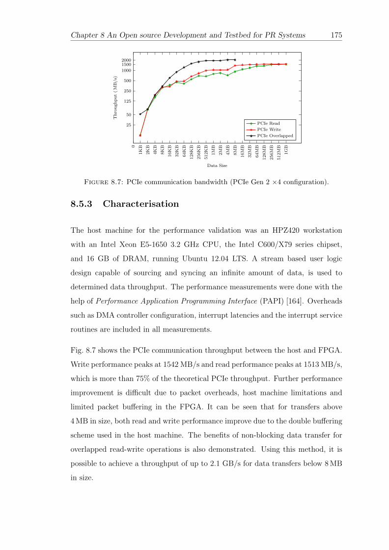
Chapter 8 An Open source Development and Testbed for PR Systems 175
0
1KB
2KB
4KB
8KB
16KB
32KB
64KB
128KB
256KB
512KB
1MB
2MB
4MB
8MB
16MB
32MB
64MB
128MB
256MB
512MB
1GB
25
50
125
250
500
1000
15002000
Data Size
Throughput(MB/s)
PCIe Read
PCIe Write
PCIe Overlapped
Figure 8.7: PCIe communication bandwidth (PCIe Gen 2 ×4 configuration).
8.5.3 Characterisation
The host machine for the performance validation was an HPZ420 workstation
with an Intel Xeon E5-1650 3.2 GHz CPU, the Intel C600/X79 series chipset,
and 16 GB of DRAM, running Ubuntu 12.04 LTS. A stream based user logic
design capable of sourcing and syncing an infinite amount of data, is used to
determined data throughput. The performance measurements were done with the
help of Performance Application Programming Interface (PAPI) [164]. Overheads
such as DMA controller configuration, interrupt latencies and the interrupt service
routines are included in all measurements.
Fig. 8.7 shows the PCIe communication throughput between the host and FPGA.
Write performance peaks at 1542 MB/s and read performance peaks at 1513 MB/s,
which is more than 75% of the theoretical PCIe throughput. Further performance
improvement is difficult due to packet overheads, host machine limitations and
limited packet buffering in the FPGA. It can be seen that for transfers above
4 MB in size, both read and write performance improve due to the double buffering
scheme used in the host machine. The benefits of non-blocking data transfer for
overlapped read-write operations is also demonstrated. Using this method, it is
possible to achieve a throughput of up to 2.1 GB/s for data transfers below 8 MB
in size.
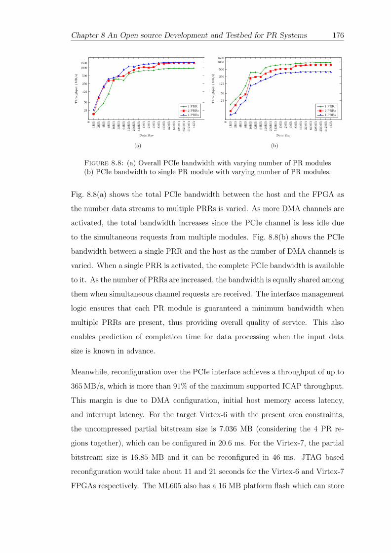
Chapter 8 An Open source Development and Testbed for PR Systems 176
0
1KB
2KB
4KB
8KB
16KB
32KB
64KB
128KB
256KB
512KB
1MB
2MB
4MB
8MB
16MB
32MB
64MB
128MB
256MB
512MB
1GB
25
50
125
250
500
1000
1500
Data Size
Throughput(MB/s)
1 PRR
2 PRRs
4 PRRs
(a)
0
1KB
2KB
4KB
8KB
16KB
32KB
64KB
128KB
256KB
512KB
1MB
2MB
4MB
8MB
16MB
32MB
64MB
128MB
256MB
512MB
1GB
25
50
125
250
500
1000
1500
Data Size
Throughput(MB/s)
1 PRR
2 PRRs
4 PRRs
(b)
Figure 8.8: (a) Overall PCIe bandwidth with varying number of PR modules(b) PCIe bandwidth to single PR module with varying number of PR modules.
Fig. 8.8(a) shows the total PCIe bandwidth between the host and the FPGA as
the number data streams to multiple PRRs is varied. As more DMA channels are
activated, the total bandwidth increases since the PCIe channel is less idle due
to the simultaneous requests from multiple modules. Fig. 8.8(b) shows the PCIe
bandwidth between a single PRR and the host as the number of DMA channels is
varied. When a single PRR is activated, the complete PCIe bandwidth is available
to it. As the number of PRRs are increased, the bandwidth is equally shared among
them when simultaneous channel requests are received. The interface management
logic ensures that each PR module is guaranteed a minimum bandwidth when
multiple PRRs are present, thus providing overall quality of service. This also
enables prediction of completion time for data processing when the input data
size is known in advance.
Meanwhile, reconfiguration over the PCIe interface achieves a throughput of up to
365 MB/s, which is more than 91% of the maximum supported ICAP throughput.
This margin is due to DMA configuration, initial host memory access latency,
and interrupt latency. For the target Virtex-6 with the present area constraints,
the uncompressed partial bitstream size is 7.036 MB (considering the 4 PR re-
gions together), which can be configured in 20.6 ms. For the Virtex-7, the partial
bitstream size is 16.85 MB and it can be reconfigured in 46 ms. JTAG based
reconfiguration would take about 11 and 21 seconds for the Virtex-6 and Virtex-7
FPGAs respectively. The ML605 also has a 16 MB platform flash which can store
Chapter 8 An Open source Development and Testbed for PR Systems 177
a single bitstream with reconfiguration taking about 100 ms. The VC707 has a
128 MB BPI flash which can store up to 4 bitstreams and reconfiguration takes
130 ms. Storing bitstreams in the flash is a time consuming operation taking up
to 20 minutes on ML605 and 30 minutes on the VC707. Hence, none of these
other reconfiguration approaches makes sense for dynamically reconfiguring user
logic, especially if this is done for an accelerator within a larger software program,
where such latency can nullify any performance advantage.
Reconfiguration performance can also be improved by enabling bitstream compres-
sion with the amount of compression dependent on the logic in the circuit. For the
user logic in the subsequent case study, containing 1577 registers and 1464 LUTs,
the partial bitstream size was reduced to 1.29 MB, which could be reconfigured in
under 3.6 ms.
8.5.4 Case Study
To demonstrate the effectiveness of the proposed framework in the context of a
software application with hardware accelerators, an example video processing ap-
plication was implemented and tested. The application implements several filters:
a thresholder, inverter, Gaussian filter, Laplace filter and Sobel edge detector.
These were implemented in user logic running at 250MHz with a 64-bit stream-
ing interface. Multiple filters can be configured concurrently in adjacent PRRs
to create more filter effects. The application processes a continuous stream of
640×480 greyscale video frames with 1 Byte/pixel resolution, to produce a con-
tinuous stream of output data. As a streaming application, the hardware latency
is purely a function of the pipeline. Identical filters are implemented in software
on the host (using C) for performance comparison.
Partial bitstreams corresponding to each of these filters are stored in a bitstream
library in the host machine. Data is sent and received from the FPGA board
using the API in non-blocking mode (streaming). The software application can
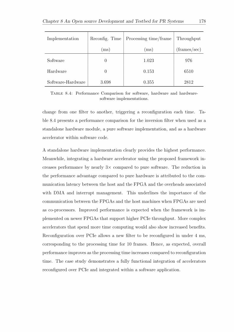
Chapter 8 An Open source Development and Testbed for PR Systems 178
Implementation Reconfig. Time Processing time/frame Throughput
(ms) (ms) (frames/sec)
Software 0 1.023 976
Hardware 0 0.153 6510
Software-Hardware 3.698 0.355 2812
Table 8.4: Performance Comparison for software, hardware and hardware-software implementations.
change from one filter to another, triggering a reconfiguration each time. Ta-
ble 8.4 presents a performance comparison for the inversion filter when used as a
standalone hardware module, a pure software implementation, and as a hardware
accelerator within software code.
A standalone hardware implementation clearly provides the highest performance.
Meanwhile, integrating a hardware accelerator using the proposed framework in-
creases performance by nearly 3× compared to pure software. The reduction in
the performance advantage compared to pure hardware is attributed to the com-
munication latency between the host and the FPGA and the overheads associated
with DMA and interrupt management. This underlines the importance of the
communication between the FPGAs and the host machines when FPGAs are used
as co-processors. Improved performance is expected when the framework is im-
plemented on newer FPGAs that support higher PCIe throughput. More complex
accelerators that spend more time computing would also show increased benefits.
Reconfiguration over PCIe allows a new filter to be reconfigured in under 4 ms,
corresponding to the processing time for 10 frames. Hence, as expected, overall
performance improves as the processing time increases compared to reconfiguration
time. The case study demonstrates a fully functional integration of accelerators
reconfigured over PCIe and integrated within a software application.
Chapter 8 An Open source Development and Testbed for PR Systems 179
8.6 Summary
In this chapter we presented a platform which enables rapid validation of PR based
systems integrated within a host PC, with data communication and reconfiguration
managed over a PCIe interface. The DMA based streaming architecture achieves
more than 75% of theoretical PCIe bandwidth. Partial reconfiguration over PCIe
reduces reconfiguration time to a few milliseconds compared to several seconds for
JTAG. An API provides functions that make integration easier, and allow for the
use of accelerators in software applications on the host. The unified communication
and reconfiguration infrastructure avoids the need for proprietary software drivers
and dedicated external wiring to the JTAG port. An example application was
implemented, demonstrating the reconfiguration, and data throughput capabilities
of the platform.
Chapter 9
Conclusions and Future work
This dissertation has proposed a framework that enables high-level design of adap-
tive systems using FPGA partial reconfiguration (PR). It has shown that FPGAs
are suitable hardware platforms for high-performance adaptive systems implemen-
tation and that PR offers advantages for such systems. The suitability of hybrid
FPGA platforms, which integrate processors with reconfigurable fabric on the
same physical chip, has also been demonstrated. An open-source verification plat-
form, DyRACT, has also been introduced, making hardware verification of PR
based designs easier and less time consuming. We also presented CoPR for Zynq,
a fully automated flow for implementing PR-based adaptive systems on the Zynq
platform.
This chapter draws the conclusions from the dissertation, highlights its contribu-
tions, and outlines areas for further research.
9.1 Summary of Contributions
The proposed PR based adaptive system development framework can be broadly
classified into two parts: design-time PR methods and tools, and run-time PR
support. Design time methods and tools provide support to the designer during
the hardware design stage of the system. Specifically speaking, we have automated
180

Chapter 9 Conclusions and Future work 181
several operations that previously required manual steps by the designer, showing
that these could help optimise overall system efficiency. The run-time PR support
provides run-time management of reconfiguration, allows for higher level adaptive
design, and a hardware based verification platform to help with testing.
9.1.1 Partitioning and Floorplanning
Present vendor supported PR tool flows, and most of the tools developed by the
research community, require manual partitioning and floorplanning for PR de-
signs. In Chapters 4 and 5, we demonstrated the impact of these steps on system
performance and the architecture expertise required from the designer to find
efficient solutions. We proposed methods for automatic partitioning and floor-
planning by considering the architecture of the current FPGAs, and automated
these steps. The proposed methods respect all the constrains specified by the
vendor implementation tools in order to integrate the whole flow. The tools allow
different optimisation strategies, such as minimising total resource utilisation or
minimising reconfiguration time. This allows the designer to choose the required
optimisation strategy depending on requirements. The feasibility of these tools
was demonstrated through case studies.
9.1.2 Run-time PR Support and Management
The design-time contributions detailed above provide everything necessary for the
PR system to be implemented. However, true adaptive systems need intelligent
management of adaptation that is typically better done in software. During the
design stage, the proposed tools build necessary infrastructure and interfaces for
the management of PR. During runtime the system adapts based on operational
conditions. Present development flows require adaptation to be explicitly coded
by the designer, who must explicitly state which bitstreams to load making the
software designer essentially the system designer. Furthermore, the performance
achievable with vendor provided reconfiguration infrastructure is poor.
Chapter 9 Conclusions and Future work 182
In Chapter 7, we presented a design framework that allows designers with less
hardware expertise to specify complex adaptation using a high level system spec-
ification. The designer considers only the configurations they are aware of from
the abstract perspective and our tools and runtime system translate this to the
low level reconfiguration steps required to enact the appropriate reconfiguration.
In Chapter 6, we developed two custom reconfiguration controllers, one targeting
traditional FPGA architectures and one targeting hybrid FPGA platforms such
as the Zynq. The controllers achieve near theoretical reconfiguration performance,
thus reducing reconfiguration time substantially while not overburdening the re-
configuration management processor with low-level reconfiguration operations.
9.1.3 Automated PR Development Flow
In Chapter 7, we developed a fully automated PR development flow, called CoPR
for Zynq, targeting hybrid FPGA platforms. A high-level system specification
model is proposed which enables system-level developers to easily compose adap-
tive systems using pre-designed IP cores. The proposed partitioning and floorplan-
ning algorithms were integrated with the vendor implementation flow to create a
complete development flow. It also allows the designer to integrate our custom
ICAP controller (ZyCAP) to achieve near theoretical reconfiguration performance.
The run-time reconfiguration management was also adapted to the hybrid FPGA
platform, which made reconfiguration management easier and independent of the
adaptation logic.
9.1.4 PR verification platform
Finally, in Chapter 8, we introduced an open-source PR system verification plat-
form called DyRACT. PR based hardware verification is more challenging com-
pared to traditional FPGA designs and the communication infrastructure required
for such a platform is tedious to develop. The proposed platform along with the
implementation framework enables users to quickly integrate their PR designs
Chapter 9 Conclusions and Future work 183
with the communication and reconfiguration infrastructure. We demonstrated
that using the same PCIe communication channel, near theoretical reconfigura-
tion performance can be achieved along with high communication throughput.
We also presented the virtual-channel-based PCIe communication infrastructure,
which is scalable while saturating at more than 75% of the PCIe bandwidth.
9.2 Future Research Directions
The research reported in this thesis was intended to cover the whole automated
design flow. As such, we have identified a number of interesting research questions
that can be explored in each of these aspects of PR design that we propose be
explored in future work.
9.2.1 Combined Partitioning and Floorplanning
The partitioning and floorplanning tools we proposed operate in sequence with
the floorplanner using the regions determined during partitioning. It might be
possible that a proposed partitioning cannot be floorplanned on the FPGA due
to the spatial arrangement of resources. This would require determination of a
new partitioning. We also saw in Chapter 5 that the rectangular region constraint
sometimes results in wasted extra resources. Combining the two steps together so
that the partitioning algorithm takes into account these limitations might lead to
more predictably achievable floorplans.
In this work, we optimise for total reconfiguration time, based on valid configu-
rations. This can be enhanced by considering only valid configuration transitions
as specified in the adaptation specification. Such optimisations have been demon-
strated for PR implementation of static task graphs, but similar information could
be determined from the adaptation specification of an adaptive system. Further-
more, it might be possible to incorporate measured probabilities of transition to
further enhance the real overall metrics.
Chapter 9 Conclusions and Future work 184
9.2.2 Operating System Support
The reconfiguration manager for Zynq and the driver for ZyCAP have so far been
implemented for the Standalone operating system, a lightweight, vendor-provided
operating system offering high performance but limited features. To attract a
wider interest and to make the framework more portable and accessible, the frame-
work should be ported to an operating system such as Linux, or a real time op-
erating system. This would also allow application designers to use other libraries
in the control plane. Managing reconfiguration within an OS is feasible, but adds
some latency. Providing a more low-level interface that still supports OS inter-
action would be of benefit. An example is the use of a Microkernel hypervisor
to manage the PR process [165]. Understanding how to manage PR within the
context of real operating systems is an area that requires further research.
9.2.3 Integration with HLS tools
The increasing popularity of high-level synthesis (HLS) techniques is a great mo-
tivation for integrating the PR implementation framework with HLS tools such
as Xilinx’s Vivado-HLS. By doing so, the HLS tools can directly use C based
module descriptions and generate corresponding RTL modules, which can be used
by the proposed automation tools and vendor implementation tools for the final
implementation. The HLS tools can integrate more tightly with the proposed
framework, allowing for a design space exploration that includes partial reconfigu-
ration as a consideration. The present automation scripts should also be updated
to function with the new Xilinx Vivado design suite.
9.2.4 Domain Specific IP Libraries
Creating a framework that enables a block-based approach to PR design means
designers will be looking more at the “big picture” adaptation, and would like to
use existing IP for the data plane. It would be beneficial to the community for
Chapter 9 Conclusions and Future work 185
well-tested, well-documented libraries of blocks to be developed for different do-
mains, such as software defined radio, video and image processing and automotive
systems. Designers can then easily integrate these cores into their systems, and
work on the upper layers of the adaptive system. Adoption of a standard AXI
interface by Xilinx for their new IP cores, and similar efforts in the open source
community will help ensure interoperability.
9.2.5 PR Design Benchmarks
A major stumbling block in PR research is the lack of a standard set of PR
benchmarks for comparing PR tools. This often forces researchers to resort to
synthetic circuits or simple examples to demonstrate their proposed algorithms.
As a growing research field, a standard set of benchmarks should be developed to
allow easier validation and comparison of proposed methods in this domain.
9.3 Summary
This dissertation has contributed towards enabling high-level design of adaptive
systems through the partial reconfiguration of FPGAs. Special focus was given
to hybrid FPGAs and this is one of the first pieces of work to demonstrate their
potential in a complete system implementation. A number of open source tools and
designs were released as part of this research work, which we hope will be beneficial
to FPGA community in general, and designers of partially reconfigurable systems
in particular.
Bibliography
[1] C. Claus, J. Zeppenfeld, F. Muller, and W. Stechele. Using partial-run-time
reconfigurable hardware to accelerate video processing in driver assistance
system. In Proceedings of Design, Automation & Test in Europe Conference
& Exhibition (DATE), 2007.
[2] J. Lotze, S.A. Fahmy, J. Noguera, B. Ozgul, L. Doyle, and R. Esser. Devel-
opment framework for implementing FPGA-based cognitive network nodes.
In Proceedings of IEEE Global Telecommunications Conference (GLOBE-
COM), 2009.
[3] J.P. Delahaye, J. Palicot, C. Moy, and P. Leray. Partial reconfiguration
of FPGAs for dynamical reconfiguration of a software radio platform. In
Proceedings of IST Mobile and Wireless Comms. Summit, 2007.
[4] J. Diaz, E. Ros, F. Pelayo, E.M. Ortigosa, and S. Mota. FPGA-based real-
time optical-flow system. IEEE Transactions on Circuits and Systems for
Video Technology, 16(2):274–279, 2006.
[5] Xilinx. UG585: Zynq-7000 All Programmable SoC Technical Reference Man-
ual, Mar. 2013.
[6] Altera. Cyclone V Device Overview, Oct. 2014.
[7] Ian Kuon and J. Rose. Measuring the gap between FPGAs and ASICs. IEEE
Transactions on Computer-Aided Design of Integrated Circuits and Systems
(TCAD), 26(2):203–215, Feb 2007.
186
BIBLIOGRAPHY 187
[8] Betty H.C. Cheng, Pete Sawyer, Nelly Bencomo, and Jon Whittle. A goal-
based modeling approach to develop requirements of an adaptive system
with environmental uncertainty. In Model Driven Engineering Languages
and Systems, volume 5795, pages 468–483. Springer Berlin Heidelberg, 2009.
[9] T. Raikovich and B. Feher. Application of partial reconfiguration of FPGAs
in image processing. In Proceedings of Conference on Ph.D. Research in
Microelectronics and Electronics (PRIME), 2010.
[10] H. Lufei and W. Shi. An adaptive encryption protocol in mobile computing.
In Wireless Network Security, pages 43–62. Springer US, 2007.
[11] B. H. C. Cheng, H. Giese, P. Inverardi, J. Magee, and R. de Lemos. Soft-
ware engineering for self-adaptive systems: A research roadmap. In Soft-
ware Engineering for Self-Adaptive Systems, volume 5525 of Lecture Notes
in Computer Science, pages 1–26. Springer Berlin Heidelberg, 2009.
[12] K. Tan, H. Liu, J. Zhang, Y. Zhang, F. Yongguang, N. Fang, and G.M.
Voelker. SORA: high-performance software radio using general-purpose
multi-core processors. Communications of the ACM, 54(1):99–107, 2011.
[13] J. Becker, A. Donlin, and M. Huebner. New tool support and architectures
in adaptive reconfigurable computing. In Proceedings of IFIP International
Conference on Very Large Scale Integration (VLSI - SoC), pages 134–139,
2007.
[14] Actel. ProASIC3 Flash FPGAs, 2010.
[15] M. Peattie. Using a microprocessor to configure Xilinx FPGAs via slave
serial or SelectMAP mode. Technical report, Xilinx Inc., 2009.
[16] Xilinx Inc. DS586: XPS HWICAP, July 2010.
[17] W. Chong, S. Ogata, M. Hariyama, and M. Kameyama. Architecture of
a multi-context FPGA using reconfigurable context memory. In Proceed-
ings of IEEE International Parallel and Distributed Processing Symposium
(IPDPS), page 144a, 2005.
BIBLIOGRAPHY 188
[18] R.T. Ong. Programmable logic device which stores more than one configu-
ration and means for switching configurations., Jun 1995.
[19] S. Trimberger, D. Carberry, A. Johnson, and J. Wong. A time-multiplexed
FPGA. In Proceedings of IEEE Symposium on FPGAs for Custom Comput-
ing Machines (FCCM), pages 22–28, 1997.
[20] I. Kennedy. Exploiting redundancy to speedup reconfiguration of an FPGA.
In Proceedings of International Conference on Field Programmable Logic and
Applications (FPL), pages 262–271, 2003.
[21] E. Tau, I. Eslick, D. Chen, J. Brown, and A. DeHon. A first generation
DPGA implementation. In Proceedings of the Canadian Workshop on Field-
Programmable Devices (FPD), pages 138–143, 1995.
[22] A. DeHon. DPGA utilization and application. In Proceedings of
ACM/SIGDA International Symposium on FPGAs, pages 115–121, 1996.
[23] S.M. Scalera and J.R. Vazquez. The design and implementation of a context
switching FPGA. In Proceedings of IEEE Symposium on FPGAs for Custom
Computing Machines (FCCM), pages 78–85, 1998.
[24] J.R. Hauser and J. Wawrzynek. GARP: a MIPS processor with a recon-
figurable coprocessor. In Proceedings of The Annual IEEE Symposium on
Field-Programmable Custom Computing Machines (FCCM), pages 12–21,
1997.
[25] Xilinx Inc. Programmable Logic Data Book, 1996.
[26] Xilinx Inc. DS031:Virtex-II Platform FPGAs, 2003.
[27] Xilinx Inc. DS083: Virtex-II Pro and Virtex-II Pro-X Platform FPGAs,
2011.
[28] Xilinx Inc. XAPP151: Virtex Series Configuration Architecture User Guide,
2004.
[29] Xilinx Inc. UG070: Virtex-4 FPGA User Guide, 2008.

BIBLIOGRAPHY 189
[30] P. Lysaght, B. Blodget, J. Mason, J. Young, and B. Bridgford. Invited paper:
Enhanced architectures, design methodologies and CAD tools for dynamic
reconfiguration of xilinx FPGAs. In Proceedings of International Conference
on Field Programmable Logic and Applications (FPL), 2006.
[31] Xilinx Inc. UG191: Virtex-5 FPGA Configuration User Guide, 2010.
[32] Altera Corporation. Design Planning for Partial Reconfiguration, Nov. 2013.
[33] National. Configurable Logic Array (CLAy) Data Sheet. National Semicon-
ductor, 1993.
[34] Lattice Semiconductor Corporation. ORCA Series 4 FPGAs, March 2003.
[35] Atmel. AT40K series configuration. Technical report, Atmel, 2002.
[36] Tabula. Spacetime architecture. Technical report, Tabula, 2010.
[37] Altera. SIV52005: Dynamic Reconfiguration in Stratix IV Devices, 2005.
[38] Xilinx Inc. UG682: PlanAhead User Guide, Jun. 2013.
[39] E. Eto. XAPP290: Difference-based partial reconfiguration. Technical re-
port, Xilinx Inc., 2007.
[40] Altera Corp. Quartus II Handbook Version 13.1, Nov. 2013.
[41] A.A. Sohanghpurwala, P. Athanas, T. Frangieh, and A. Wood. OpenPR: An
open-source partial-reconfiguration toolkit for Xilinx FPGAs. In Proceedings
of IEEE International Symposium on Parallel and Distributed Processing
Workshops and Phd Forum (IPDPSW), pages 228–235, 2011.
[42] N. Steiner, A. Wood, H. Shojaei, J. Couch, P. Athanas, and M. French. Torc
: Towards an open-source tool flow. In Proceedings of ACM/SIGDA Inter-
national Symposium on Field-Programmable Gate Arrays (FPGA), 2011.
[43] C. Beckhoff, D. Koch, and J. Torresen. GoAhead: A partial reconfigura-
tion framework. In Proceeding of IEEE International Symposium on Field-
Programmable Custom Computing Machines (FCCM), pages 37–44, 2012.
BIBLIOGRAPHY 190
[44] J. Harkin, T.M. Mcginnity, and L.P. Maguire. Modeling and optimizing run-
time reconfiguration using evolutionary computation. ACM Transactions on
Embedded Computing Systems (TECS), 3(4):661–685, Nov. 2004.
[45] W. Luk, N. Shirazi, and P.Y.K. Cheung. Modelling and optimising run-time
reconfigurable systems. In Proceedings of IEEE Symposium on FPGAs for
Custom Computing Machines (FCCM), 1996.
[46] Alberto Donato, Fabrizio Ferrandi, Massimo Redaelli, MarcoDomenico San-
tambrogio, and Donatella Sciuto. Caronte: A methodology for the imple-
mentation of partially dynamically self-reconfiguring systems on FPGA plat-
forms. In VLSI-Soc: From Systems To Silicon, volume 240, pages 87–109.
Springer US, 2007.
[47] I. Robertson and J. Irvine. A design flow for partially reconfigurable
hardware. ACM Transactions on Embedded Computing Systems (TECS),
3(2):257–283, May 2004.
[48] M. Boden, T. Fiebig, M. Reiband, and P. Reichel. GePaRD - a high-level
generation flow for partially reconfigurable designs. In Proceedings of IEEE
Computer Society Annual Symposium on VLSI (ISVLSI), 2008.
[49] N. Abel. Design and implementation of an object-oriented framework for
dynamic partial reconfiguration. In Proceedings of International Conference
on Field Programmable Logic and Applications (FPL), 2010.
[50] S.A. Fahmy, J. Lotze, J. Noguera, L. Doyle, and R. Esser. Generic software
framework for adaptive applications on FPGAs. In Proceedings of IEEE
Symposium on Field-Programmable Custom Computing Machines (FCCM),
pages 55–62, 2009.
[51] H. Tan and R.F. DeMara. A multilayer framework supporting autonomous
run-time partial reconfiguration. IEEE Transactions on Very Large Scale
Integration (VLSI) Systems, 16(5):504–516, May 2008.
BIBLIOGRAPHY 191
[52] K. Bazargan, R. Kastner, and M. Sarrafzadeh. Fast template placement for
reconfigurable computing systems. IEEE Design and Test of Computers,
17(1):68–83, Jan 2000.
[53] Y. Lu, T. Marconi, G.N. Gaydadjiev, K. Bertels, and R.J. Meeuws. A
self-adaptive on-line task placement algorithm for partially reconfigurable
systems. In Proceedings of Parallel and Distributed Processing Symposium
(IPDPS), 2008.
[54] S. Raaijmakers and S. Wong. Run-time partial reconfiguration for removal,
placement and routing on the Virtex-II Pro. In Proceedings of International
Conference on Field Programmable Logic and Applications (FPL), 2007.
[55] S P. Fekete, J C. van der Veen, A. Ahmadinia, D. G?hringer, M. Majer, and
J. Teich. Offline and online aspects of defragmenting the module layout of
a partially reconfigurable device. IEEE Transactions on Very Large Scale
Integration (VLSI) Systems, 16(9):1210–1219, Sept. 2008.
[56] K. Compton, Z. Li, J. Cooley, and S. Knol. Configuration relocation and
defragmentation for run-time reconfigurable computing. IEEE Transactions
on VLSI Systems, 10(3):209–220, 2002.
[57] M. Koester, W. Luk, J. Hagemeyer, and M. Porrmann. Design optimizations
to improve placeability of partial reconfiguration modules. In Proceedings
of Design, Automation & Test in Europe Conference & Exhibition (DATE),
2009.
[58] T. Becker, W. Luk, and P.Y.K. Cheung. Enhancing relocatability of partial
bitstreams for run-time reconfiguration. In Proceedings of IEEE Symposium
on Field-Programmable Custom Computing Machines (FCCM), 2007.
[59] E.L. Horta and J.W. Lockwood. PARBIT: A Tool to Transform Bitfiles
to Implement Partial Reconfiguration of FIeld Programmable Gate Arrays
(FPGA). Washington University, 2001.
BIBLIOGRAPHY 192
[60] H. Kalte, G. Lee, M. Porrmann, and U. Ruckert. REPLICA: A bitstream
manipulation filter for module relocation in partial reconfigurable systems.
In Proceedings of IEEE International Parallel and Distributed Processing
Symposium (IPDPS), 2005.
[61] H. Kalte and M. Porrmann. REPLICA2Pro: Task relocation by bitstream
manipulation in Virtex-II/Pro FPGAs. In Proceedings of conference on Com-
puting frontiers, 2006.
[62] S. Guccione, D. Levi, and P. Sundararajan. JBits: Java based interface for
reconfigurable computing. Technical report, Xilinx Inc., 2004.
[63] J. H. Pan, T. Mitra, and W. Wong. Configuration bitstream compression
for dynamically reconfigurable FPGAs . In Proceedings of IEEE/ACM In-
ternational Conference on Computer Aided Design (ICCAD), 2004.
[64] S. Hauck, Z. Li, and E. Schwabe. Configuration compression for the xilinx
XC6200 FPGA. In Proceedings of IEEE Symposium on FPGAs for Custom
Computing Machines (FCCM), 1998.
[65] S. Hauck, Z. Li, and E. Schwabe. Configuration compression for the xilinx
XC6200 FPGA. In Proceedings of IEEE Transactions on Computer-Aided
Design of Integrated Circuits and Systems, 1999.
[66] Z. Li and S. Hauck. Configuration compression for virtex FPGAs. In Pro-
ceedings of IEEE Symposium on Field-Programmable Custom Computing
Machines (FCCM), 2001.
[67] G. Haiyun and C. Shurong. Partial reconfiguration bitstream compression for
Virtex FPGAs. In Proceedings of Congress on Image and Signal Processing
(CISP), 2008.
[68] Z. Li, K. Compton, and S. Hauck. Configuration caching management tech-
niques for reconfigurable computing. In IEEE Symposium on FPGAs for
Custom Computing Machines (FCCM), 2000.
BIBLIOGRAPHY 193
[69] S. Ghiasi and M. Sarrafzadeh. Optimal reconfiguration sequence manage-
ment. In Proceedings of Asia and Sourth Pacific Design Automation Con-
ference (ASP-DAC), 2003.
[70] S. Ghiasi, A. Nahapetian, and M. Sarrafzadeh. An optimal algorithm for
minimizing run-time reconfiguration delay. ACM Transactions on Embedded
Computing Systems (TECS), 3(2):237–256, May 2004.
[71] W. Lie and W.Feng-yan. Dynamic partial reconfiguration on cognitive radio
platform. In Proceedings of IEEE International Conference on Intelligent
Computing and Intelligent Systems (ICIS), 2009.
[72] C.S. Choi and H. Lee. An reconfigurable fir filter design on a partial re-
configuration platform. In Proceedings of Communications and Electronics
(ICCE), 2006.
[73] H. Taghipour, J. Frounchi, and M. H. Zarifi. Design and implementation of
MP3 decoder using partial dynamic reconfiguration on Virtex-4 FPGAs. In
Proceedings of International Conference on Computer and Communication
Engineering, 2008.
[74] S. Bouchoux, E. Bourennane, and M. Paindavoine. Implementation of
JPEG2000 arithmetic decoder using dynamic reconfiguration of FPGA . In
Proceedings of International Conference on Image Processing (ICIP), 2004.
[75] R. Khraisha and J. Lee. A scalable H.264/AVC deblocking filter architecture
using dynamic partial reconfiguration. In Proceedings of IEEE International
Conference on Acoustics Speech and Signal Processing (ICASSP), 2010.
[76] S. U. Bhandari, S. Subbaraman, S. S. Pujari, and R. Mahajan. Real time
video processing on FPGA using on the fly partial reconfiguration. In In-
ternational Conference on Signal Processing Systems (ICSPS), 2009.
[77] M. Ceschia, M. Violante, M. Sonza Reorda, A. Paccagnella, P. Bernardi,
M. Rebaudengo, D. Bortolato, M. Bellato, P. Zambolin, and A. Candelori.
Identification and classification of single-event upsets in the configuration
BIBLIOGRAPHY 194
memory of SRAM-based FPGAs. IEEE Transactions on Nuclear Science,
50(6):2088–2094, Dec. 2003.
[78] C. Bolchini, D. Quarta, and M. D. Santambrogio. SEU mitigation for SRAM-
based FPGAs through dynamic partial reconfiguration. In Proceedings of
ACM Great Lakes symposium on VLSI, 2007.
[79] C. Bolchini, A. Miele, and M. D. Santambrogio. TMR and partial dynamic
reconfiguration to mitigate SEU faults in FPGAs. In Proceedings of IEEE
International Symposium on Defect and Fault Tolerance in VLSI Systems
(DFT), 2007.
[80] J. Heiner, B. Sellers, M. Wirthlin, and J. Kalb. FPGA partial reconfiguration
via configuration scrubbing. In Proceedings of International Conference on
Field Programmable Logic and Applications ((FPL), 2009.
[81] C. Carmichael. XAPP216: Correcting Single-Event Upsets Through Virtex
Partial Configuration. Xilinx Inc., June 2000.
[82] C. Carmichael. XAPP197: Triple Module Redundancy Design Techniques
for Virtex FPGAs. Xilinx Inc., July 2006.
[83] B. Osterloh, H. Michalik, S. A. Habinc, and B. Fiethe. Dynamic partial
reconfiguration in space applications. In Proceedings of NASA/ESA Confer-
ence on Adaptive Hardware and Systems, 2009.
[84] J. W. Lockwood, N. Naufel, J. S. Turner, and D. E. Taylor. Reprogrammable
network packet processing on the field programmable port extender (FPX).
In Proceedings of ACM/SIGDA International Symposium on Field Pro-
grammable Gate Arrays (FPGA), 2001.
[85] D. Yin, D. Unnikrishnan, Y. Liao, L. Gao, and R. Tessier. Customizing vir-
tual networks with partial FPGA reconfiguration. ACM SIGCOMM Com-
puter Communication Review, 41(1):57–64, Jan. 2011.
BIBLIOGRAPHY 195
[86] J. Noguera and I.O. Kennedy. Power reduction in network equipment
through adaptive partial reconfiguration. In Proceedings of International
Conference on Field Programmable Logic and Applications (FPL), 2007.
[87] C. Claus, W. Stechele, and A. Herkersdorf. Autovision - a run-time reconfig-
urable MPSoC architecture for future driver assistance systems. Information
Technology, 49:181–186, 2007.
[88] S. Shreejith, K. Vipin, S.A. Fahmy, and M. Lukasiewycz. An approach for
redundancy in flexray networks using FPGA partial reconfiguration. In Pro-
ceedings of the Design, Automation and Test in Europe Conference (DATE),
2013.
[89] W. Gao, K. Kugel, R. Manner, N. Abel, N. Meier, and U. Kebschull. DPR
in high energy physics. In Proceedings of Design, Automation & Test in
Europe Conference & Exhibition (DATE), 2009.
[90] K. Papadimitriou, A. Anyfantis, and A. Dollas. An effective framework to
evaluate dynamic partial reconfiguration in FPGA systems. IEEE Transac-
tions on Instrumentation and Measurement, 59(6):1642–1651, June 2010.
[91] M.J. Wirthlin and B.L. Hutchings. A dynamic insruction set computer. In
In IEEE Symposium on FPGAs for Custom Computing Machines, 1995.
[92] E. El-Araby, I. Gonzale, and T. El-Ghazawi. Performance bounds of partial
run-time reconfiguration in high-performance reconfigurable computing. In
Proceedings of International Workshop on High-Performance Reconfigurable
Computing Technology and Applications (HPRCTA), 2007.
[93] N.J. Steiner. Autonomous Computing Systems. PhD thesis, Virginia Poly-
technic Institute and State University, 2008.
[94] S. Byma, J.G. Steffan, H. Bannazadeh, A. Leon-Garcia, and P. Chow. FP-
GAs in the cloud: Booting virtualized hardware accelerators with Open-
Stack. In Proceedings of the IEEE International Symposium on Field-
Programmable Custom Computing Machines (FCCM), pages 109–116, 2014.

BIBLIOGRAPHY 196
[95] S. Kestur, J.D. Davis, and O. Williams. BLAS comparison on FPGA, CPU
and GPU. In Proceedings of the IEEE Computer Society Annual Symposium
on VLSI (ISVLSI), pages 288–293, 2010.
[96] S. Asano, T. Maruyama, and Y. Yamaguchi. Performance comparison of
FPGA, GPU and CPU in image processing. In Proceedings of the Inter-
national Conference on Field Programmable Logic and Applications (FPL),
pages 126–131, 2009.
[97] J. Torresen, G.A. Senland, and K. Glette. Partial reconfiguration applied in
an on-line evolvable pattern recognition system. In The Nordic Microelec-
tronics event (NORCHIP), 2008.
[98] M. Birla and K.N. Vikram. Partial run-time reconfiguration of FPGA for
computer vision applications. In Proceedings of IEEE International Sympo-
sium on Parallel and Distributed Processing (IPDPS), 2008.
[99] K. Vipin and S. A. Fahmy. Efficient region allocation for adaptive partial
reconfiguration. In Proceedings of the International Conference on Field
Programmable Technology (FPT), pages 1–6, 2011.
[100] K. Vipin and S. A. Fahmy. Automated partitioning for partial reconfig-
uration design of adaptive systems. In Proceedings of the Reconfigurable
Architectures Workshop (RAW), pages 172–181, may 2013.
[101] S. Ganesan and R. Vemuri. An integrated temporal partioning and partial
reconfiguration technique for design latency improvement. In Proceedings of
Design, Automation and Test in Europe (DATE), pages 320–325, 2000.
[102] Z. Li and S. Hauck. Configuration prefetching techniques for partial recon-
figurable coprocessor with relocation and defragmentation. In Proceedings
of ACM/SIGDA Symposium on Field-Programmable Gate Arrays (FPGA),
2002.
BIBLIOGRAPHY 197
[103] V. Rana, S. Murali, D. Atienza, M. D. Santambrogio, L. Benini, and D. Sci-
uto. Minimization of the reconfiguration latency for the mapping of ap-
plications on FPGA-based systems. In Proceedings of IEEE/ACM Inter-
national Conference on Hardware/software Codesign and System Synthesis
(CODES+ISSS), 2009.
[104] A. Jara-Berrocal and A. Gordon-Ross. Runtime temporal partitioning as-
sembly to reduce FPGA reconfiguration time. In Proceedings of the Inter-
national Conference on Reconfigurable Computing and FPGAs (ReConFig),
2009.
[105] A. Montone, M.D. Santambrogio, D. Sciuto, and S.O. Memik. Placement
and floorplanning in dynamically reconfigurable FPGAs. ACM Transactions
on Reconfigurable Technology and Systems, 3(4):24:11–24:34, Nov. 2010.
[106] Xilinx Inc. UG702: Partial Reconfiguration User Guide, 2010.
[107] LPSolve. Lpsolve reference guide.
[108] M. Liu, Z. Lu, W. Kuehn, S. Yang, and A. Jantsch. A reconfigurable design
framework for FPGA adaptive computing. In Proceedings of International
Conference on Reconfigurable Computing and FPGAs (ReConFig), 2009.
[109] M. Srinivas and C. K. Mohan. Efficient clustering approach using incre-
mental and hierarchical clustering methods. In Proceedings of International
Joint Conference on Neural Networks (IJCNN), 2010.
[110] Python programming language - official website.
[111] K. Vipin and S.A. Fahmy. A high speed open source controller for FPGA
partial reconfiguration. In Proceedings of IEEE International Conference on
Field-Programmable Technology (FPT), 2012.
[112] Xilinx Inc. DS100: Virtex-5 Family Overview, Feb. 2009.
[113] K. Vipin and S. A. Fahmy. Architecture-aware reconfiguration-centric floor-
planning for partial reconfiguration. In Proceedings of the International Sym-
posium on Applied Reconfigurable Computing (ARC), pages 13–25, 2012.

BIBLIOGRAPHY 198
[114] S.N. Adya and I.L. Markov. Fixed-outline floorplanning through better local
search. In Proceedings of ACM/IEEE International Conference on Computer
Design, pages 328 – 334, 2001.
[115] Y. Feng and D.P. Mehta. Heterogeneous floorplanning for FPGAs. In Pro-
ceedings of International Conference on VLSI Design, 2006.
[116] J. Yuan, S. Dong, X. Hong, and Y. Wu. LFF algorithm for heterogeneous
FPGA floorplanning. In Proceedings of Asia and South Pacific Design Au-
tomation Conference (ASP-DAC), pages 1123–1126, 2005.
[117] P. Banerjee, M. Sangtani, and S. Sur-Kolay. Floorplanning for partially
reconfigurable FPGAs. IEEE Transactions on Computer-Aided Design of
Integrated Circuits and Systems (TCAD), 30(1):8–17, Jan. 2011.
[118] P. Yuh, C. Yang, and Y. Chang. Temporal floorplanning using the T-tree for-
mulation. In Proceedings of IEEE/ACM International Conference on Com-
puter Aided Design (ICCAD), pages 300–305, 2004.
[119] P. Yuh, C. Yang, Y. Chang, and H. Chen. Temporal floorplanning using
3D-subTCG. In Proceedings of Asia and South Pacific Design Automation
Conference (ASP-DAC), 2004.
[120] L. Singhal and E. Bozorgzadeh. Multi-layer floorplanning for reconfigurable
designs. IET Computers & Digital Techniques, 1(4):276–294, July 2007.
[121] Y. Zhan, Y. Feng, and S. Sapatnekar. A fixed-die floorplanning algorithm
using an analytical approach. In Proceedings of Asia and South Pacific
Design Automation Conference (ASP-DAC), pages 771 – 776, 2006.
[122] M. Rabozzi, J. Lillis, and M.D. Santambrogio. Floorplanning for partially-
reconfigurable FPGA systems via mixed-integer linear programming. In Pro-
ceedings of IEEE International Symposium on Field-Programmable Custom
Computing Machines (FCCM), 2014.
[123] K. Vipin and S.A. Fahmy. Zycap: Efficient partial reconfiguration manage-
ment on the Xilinx Zynq. IEEE Embedded System Letters (ESL), 6, 2014.
BIBLIOGRAPHY 199
[124] Xilinx Inc. UG360 : Virtex 6 FPGA Configuration User Guide, Nov. 2011.
[125] Xilinx Inc. DS817: AXI HWICAP, June 2011.
[126] Xilinx Inc. DS280: OPB HWICAP, July 2006.
[127] C. Claus, F. H. Muller, J. Zeppenfeld, and W. Stechele. A new framework
to accelerate Virtex-II Pro dynamic partial self-reconfiguration. In Proceed-
ings of IEEE International Parallel and Distributed Processing Symposium
(IPDPS), pages 1 – 7, 2007.
[128] M. Hubner, D. Gohringer, J. Noguera, and J. Becker. Fast dynamic and par-
tial reconfiguration data path with low hardware overhead on Xilinx FPGAs.
In Proceedings of IEEE International Symposium on Parallel and Distributed
Processing Workshops and Phd Forum (IPDPSW), pages 1–8, 2010.
[129] S. Liu, R. N. Pittman, and A. Forin. Minimizing partial reconfiguration
overhead with fully streaming DMA engines and intelligent ICAP controller.
Technical Report MSR-TR-2009- 150, Microsoft Research, Sept. 2009.
[130] S. Gimle Hansen, D. Koch, and J. Torresen. High speed partial run-time
reconfiguration using enhanced ICAP hard macro. In Proceedings of IEEE
International Symposium on Parallel and Distributed Processing Workshops
and Phd Forum (IPDPSW), 2011.
[131] Xilinx Inc. UG86: Xilinx Memory Interface Generator (MIG) User Guide,
Sept. 2010.
[132] S. Hauck. Configuration prefetch for single context reconfigurable copro-
cessors. In Proceedings of ACM/SIGDA International Symposium on Field-
Programmable Gate Arrays (FPGA), pages 65–74, 1998.
[133] C. Claus, B. Zhang, W. Stechele, L. Braun, M. Hubner, and J. Becker. A
multi-platform controller allowing for maximum dynamic partial reconfig-
uration throughput. In Proceedings of International Conference on Field
Programmable Logic and Applications (FPL), pages 535 – 538, 2008.
BIBLIOGRAPHY 200
[134] P. Manet, D. Maufroid, L. Tosi, G. Gailliard, O. Mulertt, M. D. Ciano,
J. D. Legat, D. Aulagnier, C. Gamrat, R. Liberati, V. L. Barba, P. Cuvelier,
B. Rousseau, and P. Gelineau. An evaluation of dynamic partial reconfigura-
tion for signal and image processing in professional electronics applications.
EURASIP Journal on Embedded Systems, 2008:1–11, 2008.
[135] M. Gokhale, P. Graham, E. Johnson, N. Rollins, and M. Wirthlin. Dynamic
reconfiguration for management of radiation-induced faults in FPGAs. In
Proceedings of International Parallel and Distributed Processing Symposium
(IPDPS), page 145, 2004.
[136] E. El-Araby, I. Gonzalez, and T. El-Ghazawi. Exploiting partial run-time re-
configuration for high-performancee reconfigurable computing. ACM Trans-
actions on Reconfigurable Technology and Systems (TRETS), 1(4):21:1–
21:23, Jan. 2009.
[137] ZedBoard : Hardware User’s Guide, Jan. 2013.
[138] T. Bapty, S. Neema, J. Scott, J. Sztipanovits, and S. Asaad. Model-
integrated tools for the design of dynamically reconfigurable systems. VLSI
Design, 10(3):281–306, 2000.
[139] Jorgiano Vidal, Florent De Lamotte, Guy Gogniat, J-P Diguet, and Se-
bastien Guillet. Dynamic applications on reconfigurable systems: from UML
model design to FPGAs implementation. In Proceedings of Design, Automa-
tion & Test in Europe Conference & Exhibition (DATE), pages 1–4, 2011.
[140] K. Vipin and S.A. Fahmy. Enabling high level design of adaptive systems
with partial reconfiguration. In Proceedings of the International Conference
on Field Programmable Technology (FPT), 2011.
[141] K. Vipin and S.A. Fahmy. Automated partial reconfiguration design for
adaptive systems with CoPR for Zynq. In Proceedings of the International
Conference on Field Programmable Custom Computing Machines (FCCM),
pages 202–205, 2014.
BIBLIOGRAPHY 201
[142] J. Mitola and G Q. Maguire. Cognitive radio: making software radios more
personal. IEEE Personal Communications, 6(4):13–18, 1999.
[143] Y. Brun, G.D.M. Serugendo, C. Gacek, H. Giese, H. Kienle, M. Litoiu,
H. Mullter, M. Pezze, and M. Shaw. Software Engineering for Self-Adaptive
Systems, volume 5525. Springer Berlin Heidelberg, 2009.
[144] G. Kahn. The semantics of a simple language for parallel programming. In
Proceedings of the IFIP Congress, pages 471–475, 1974.
[145] G. Kahn and D.B. MacQueen. Coroutines and networks of parallel program-
ming. In Proceedings of the IFIP Congress, pages 993–998, 1977.
[146] E.A. Lee and T.M Parks. Dataflow process networks. Proceedings of the
IEEE, 83(5):773–801, May 1995.
[147] M. Geilen and T. Basten. Requirements on the execution of kahn process
networks. In Proceeding of European Symposium on Programming, pages
319–334, 2003.
[148] T. M. Parks. Bounded Scheduling of Process Networks. PhD thesis, Univer-
sity of California at Berkeley, 1995.
[149] ARM. AMBA 4 AXI4-Stream Protocol Specification, Mar. 2010.
[150] K. Eguro. SIRC: An extensible reconfigurable computing communication
API. In Proceedings of IEEE Annual International Symposium on Field-
Programmable Custom Computing Machines (FCCM), pages 135 – 138,
2010.
[151] Matthew Jacobsen, Yoav Freund, and Ryan Kastner. RIFFA: A Reusable In-
tegration Framework for FPGA Accelerators. In Proceedings of IEEE Inter-
national Symposium on Field-Programmable Custom Computing Machines
(FCCM), pages 216–219, April 2012.
[152] K. Vipin, S. Shreejith, D. Gunasekera, S.A. Fahmy, and N. Kapre. System-
level FPGA device driver with high-level synthesis support. In Proceedings
BIBLIOGRAPHY 202
of International Conference on Field Programmable Technology (ICFPT),
2013.
[153] K. Vipin and S.A. Fahmy. DyRACT: A partial reconfiguration enabled accel-
erator and test platform. In in Proceedings of the International Conference
on Field Programmable Logic and Applications (FPL), 2014.
[154] R. D. Chamberlain, B. Shands, and J. White. Achieving real data through-
put for an FPGA co-processor. In Proceedings of Workshop on Building
Block Engine Architectures for Computers and Networks, 2004.
[155] M. Jacobsen and R. Kastner. RIFFA 2.0: A reusable integration framework
for FPGA accelerators. In Proceedings of International Conference on Field-
Programmable Logic, pages 249 – 258, 2013.
[156] Shepard Siegel and Jim Kulp. OpenCPI HDL Infrastructure Specification.
Technical report, 2010.
[157] Lingkan Gong and O. Diessel. Resim: A reusable library for RTL simu-
lation of dynamic partial reconfiguration. In Proceedings of International
Conference on Field-Programmable Technology (FPT), pages 1–8, 2011.
[158] K. Bondalapati and V. K. Prasanna. Dynamic precision management for
loop computations on reconfigurable architectures. In Proceedings of IEEE
Symposium on Field Programmable Custom Computing Machines (FCCM),
pages 249 – 258, 1999.
[159] J.L. Tripp, H.S. Mortveit, A.A. Hansson, and M. Gokhale. Metropolitan
road traffic simulation on FPGAs. In Proceedings of IEEE Symposium on
FPGAs for Custom Computing Machines (FCCM), pages 117–126, 2005.
[160] R.J. Fong, S.J. Harper, and P.M. Athanas. A versatile framework for FPGA
field updates: an application of partial self-reconfiguration. In Proceedings
of International Workshop on Rapid Systems Prototyping, pages 117–123,
2003.
BIBLIOGRAPHY 203
[161] S. Tam and M. Kellermann. XAPP883: Fast configuration of PCI express
technology through partial reconfiguration. Technical report, Xilinx Inc.,
Nov. 2010.
[162] P.S. Ostler, M.J. Wirthlin, and J.E. Jensen. FPGA bootstrapping on PCIe
using partial reconfiguration. In Proceedings of International Conference on
Reconfigurable Computing and FPGAs (ReConFig), pages 380–385, 2011.
[163] PCI-SIG. PCI Express Base Specification Revision 1.0a, April 2003.
[164] Performance application programming interface (PAPI).
[165] A. K. Jain, K. D. Pham, J. Cui, S.A. Fahmy, and D.L. Maskell. Virtual-
ized execution and management of hardware tasks on a hybrid ARM-FPGA
platform. Journal of Signal Processing Systems (JSPS) (Accepted), 2014.