design and test results of a high voltage amplifier as … · voltage amplifier as a gyrotron body...
TRANSCRIPT

GA–A27893
DESIGN AND TEST RESULTS OF A HIGH VOLTAGE AMPLIFIER AS A GYROTRON BODY
POWER SUPPLY by
J.F. TOOKER
AUGUST 2014


GA–A27893
DESIGN AND TEST RESULTS OF A HIGH VOLTAGE AMPLIFIER AS A GYROTRON BODY
POWER SUPPLY by
J.F. TOOKER
Work supported by General Atomics IR&D Funding
GENERAL ATOMICS PROJECT 49008 AUGUST 2014

DESIGN AND TEST RESULTS OF A HIGH VOLTAGE AMPLIFIER J.F. Tooker AS A BODY AND POWER SUPPLY
GENERAL ATOMICS REPORT GA-A27893 1
I. INTRODUCTION
A new depressed collector gyrotron was proposed for the upgrade of the DIII-D electron cyclotron heating (ECH) system that would produce higher power but still stay within the voltage and current capability of the existing power supplies to reduce the cost of the upgrade. This resulted in a design target of 1.5 MW. A frequency of 117.5 GHz was selected for this gyrotron to better match the needs of future planned experiments on DIII-D. Communications and Power Industries (CPI) completed the design and fabrication of this gyrotron and initial testing demonstrated very good results for short-pulse lengths. This gyrotron has the capability to modulate the rf power from 0 to 1.5 MW using either the cathode or body power supply for modulation frequencies of 100 Hz and higher. Modulation below 100 Hz must be performed using only the cathode power supply. This offers greater flexibility for modulation and eases some of the requirements on the power supplies.
A gyrotron body power requires a variable output voltage from 0 kV up to +35 kV and up to 50 mA continuous current, with the capability to perform square-wave modulation of the voltage at up to 5 kHz. The load is basically capacitance, of up to 2.5 nF when including the cable from the power supply to the body of the gyrotron. This requires high peak currents as well as the capability to source and sink currents in order to attain the required speed of modulation. It was found that existing topologies either do not meet all these requirements or are physically large. General Atomics undertook the development of a body power supply for the DIII-D program and for potential use at other fusion research devices.
J.F. Tooker DESIGN AND TEST RESULTS OF A HIGH VOLTAGE AMPLIFIER AS A BODY AND POWER SUPPLY
GENERAL ATOMICS REPORT GA-A27893 2
II. DEVELOPMENT OF THE DESIGN OF HIGH VOLTAGE AMPLIFIER AND PROTOTYPE TEST RESULTS
The concept is a closed-loop linear amplifier that utilizes transistors connected in series to meet the required voltage. The topology is made possible by the low continuous operating current of a few tens of milliamps and the resulting low power dissipation. Similar to a basic low voltage amplifier circuit using a complementary pair of negative positive negative (NPN) and positive negative positive (PNP) transistors, the amplifier uses a string of NPN transistors in series and a string of PNP transistors in series with the output at the junction of the NPN and PNP strings, as shown in Fig. 1. The transistors are configured into modules of 1 kV, which allow the design to be easily adapted for applications at different voltage levels. Fiber-optic links send the transistor-drive signals from the ground-level control to the series-connected transistor modules. Power to the transistor modules is provided by an isolation transformer. Each transistor module has four transistors mounted on a printed circuit board (PCB) with the transistor drive circuitry.

DESIGN AND TEST RESULTS OF A HIGH VOLTAGE AMPLIFIER J.F. Tooker AS A BODY AND POWER SUPPLY
GENERAL ATOMICS REPORT GA-A27893 3
A prototype control board and four transistor modules were fabricated and tested at up to 2 kV. Initial tests were performed with two each of the NPN and PNP transistor modules in series at voltages up to 2 kV. Figure 2 shows the four modules during the initial tests. The load network consisted of a 1 nF capacitor in parallel with a 90 kΩΩ resistor, which yields a dc load current of 22 ma at 2 kV. The data from the initial tests demonstrated the concept of controlling the output voltage by using closed-loop linear amplification with series-connected transistors.
Fig. 1. A linear amplifier circuit using series connected transistors with isolated drive circuits for high voltage and high power applications.

J.F. Tooker DESIGN AND TEST RESULTS OF A HIGH VOLTAGE AMPLIFIER AS A BODY AND POWER SUPPLY
GENERAL ATOMICS REPORT GA-A27893 4
Fig. 2. Photo of the prototype transistor modules during the initial tests.
Refinements to the control of the transistors were developed after reviewing the initial results. The modified designs of the control and prototype modules were then tested at 1 kV. The tests of the modified design demonstrated improved performance. At dc, the output voltages were measured as the reference input was adjusted and the percentage error between the expected and measured voltages was ≤0.5% for output voltages ranging from 50% to 100% of the full output voltage of 1 kV. The voltage across the four transistors in a module had a maximum difference of 1.5 V.
Modulation tests were performed with a square-wave as the reference input and Fig. 3(a) and 3(b) show the test waveforms at 100 Hz and 5 kHz, respectively. The improvement to the gate-drive circuitry provided equal voltage sharing between the transistors and increased the output frequency bandwidth.
(a) (b)
Fig. 3. Test waveforms (a) at 100 Hz modulation and (b) at 5 kHz modulation.

DESIGN AND TEST RESULTS OF A HIGH VOLTAGE AMPLIFIER J.F. Tooker AS A BODY AND POWER SUPPLY
GENERAL ATOMICS REPORT GA-A27893 5
III. DESIGN OF THE FULL POWER HIGH VOLTAGE AMPLIFIER
After the testing of the prototype modules validated the concept and topology, the design of the full power high voltage amplifier was completed and fabricated. It consists of an amplifier rack, which houses the transistor modules, and a control rack with the control electronics and the high voltage dc power supply, which provides the input voltage to the transistor modules. For a maximum output voltage of 40 kV, which includes 5 kV head room above the required voltage rating, forty 1 kV N-channel transistor modules and forty 1 kV P-channel transistor modules are required. The design of the transistor modules was finalized as part of developing the design of the amplifier rack. Figure 4 shows a photo of a 1 kV transistor module.
Fig. 4. Photo of a 1 kV transistor module.
The amplifier rack has an upper drawer and a lower draw, each of which can slide fully out for installation or removal of the transistor modules. Each drawer has two rows of twenty modules each. Forty toroidal transformers are located between the rows of each drawer to provide the AC power to the forty modules. Two isolation transformers located in the bottom of the amplifier rack provide the primary ac power to the toroidal transformers: one isolation transformer energizes the top drawer and the other feeds the lower drawer. The forty 1 kV N-channel transistor modules are in the upper drawer and the forty 1 kV P-channel transistor modules in the lower drawer. Fans are in the bottom and top of the amplifier rack to provide air flow for cooling of the modules. Figure 5 is a photo of the amplifier rack with the outside panels removed in order to view the drawers and the transistor modules.

J.F. Tooker DESIGN AND TEST RESULTS OF A HIGH VOLTAGE AMPLIFIER AS A BODY AND POWER SUPPLY
GENERAL ATOMICS REPORT GA-A27893 6
Fig. 5. A photo of the amplifier rack with outside panels removed to view the N-channel transistor modules.
A dc power supply and control electronics rack was also fabricated to house the control electronics and the high voltage dc power supplies. Two 50 kV, 125 mA power supplies are in the bottom of the rack and are connected in a master-slave configuration. An energy storage capacitor (0.05 µF, 60 kV) is located in the back of this rack and provides the high-peak-current during the charging of the capacitive load. The control PCBs are in the PCB card cage near the middle of the rack and the dc power supplies for the control electronics is near the top of the rack. Figure 6 is a photo of a gyrotron body power supply, which shows the dc power source and control electronics rack next to the amplifier rack.

DESIGN AND TEST RESULTS OF A HIGH VOLTAGE AMPLIFIER J.F. Tooker AS A BODY AND POWER SUPPLY
GENERAL ATOMICS REPORT GA-A27893 7
Fig. 6. Photo of a gyrotron body power supply.
A dummy load was designed and fabricated for testing the high voltage amplifier. It has twenty series-connected 40 kΩΩ resistors, giving a total resistance of 800 kΩΩ, and twenty series-connected 0.01 µF (or 0.047 µF) capacitors, and a fan for cooling.

J.F. Tooker DESIGN AND TEST RESULTS OF A HIGH VOLTAGE AMPLIFIER AS A BODY AND POWER SUPPLY
GENERAL ATOMICS REPORT GA-A27893 8
IV. TEST RESULTS Before the modules were assembled into the amplifier rack, they were bench-tested to
verify proper voltage sharing between the transistors. Because the dc input power is limited in the bench test, the modules were tested in groups of ten N-channel and ten P-channel transistor modules at one time. The testing started with three pairs of the N-channel and P-channel modules at an input voltage of 3 kV. An additional pair was added to the group in each step and the input voltage was increased by 1 kV, until the number of pairs reached ten and the input voltage reached 10 kV. The references were set so that the output voltages always read about half of the input voltages. In this arrangement the N-channel transistor modules are in a conducting state that results in the regulated output voltage. The P-channel transistor modules are in a non-conducting state and the voltage sharing between the P-channel transistors is determined by the voltage drop across the voltage sharing resistors. Figure 7 and Figure 8 show the graphs of the voltage sharing across the N-channel and the P-channel transistors with their average voltages, respectively (note: the y-axes have an off-set zero scale). The average voltage sharing across the N-channel transistors is 126.7 V and the standard deviation is 6.2 V (4.9%). The average voltage sharing across the P-channel transistors is 120.4 V and the standard deviation is 0.7 V (0.6%).
Fig. 7. Graph of voltages across N-channel transistors and their average voltage.

DESIGN AND TEST RESULTS OF A HIGH VOLTAGE AMPLIFIER J.F. Tooker AS A BODY AND POWER SUPPLY
GENERAL ATOMICS REPORT GA-A27893 9
Fig. 8. Graph of voltages across P-channel transistors and their average voltage.
The completed amplifier was first tested into the dummy load, which had a load resistance of 800 kΩΩ and a total load capacitance of 1.2 nF (0.5 nF in the dummy load and 0.7 nF from the output coaxial cable).
A test was performed for dc output over the range of 0 V to 35 kV. Table 1 shows the data of the input references (Vref), the measured output voltages (Vout), and the percentage of error between the expected and measured output voltages. The data in the table shows the percent of error is equal or lower than 0.2% over the full range of output voltage.
Table 1: DC Output Voltage Test
Vref (V) Vout (kV) % of error
0.00 0.00 0
0.50 5.00 0
1.00 10.01 0.1
1.50 15.02 0.13
2.00 20.03 0.15
2.50 25.05 0.2
3.00 30.06 0.2
3.50 35.07 0.2

J.F. Tooker DESIGN AND TEST RESULTS OF A HIGH VOLTAGE AMPLIFIER AS A BODY AND POWER SUPPLY
GENERAL ATOMICS REPORT GA-A27893 10
Figures 9, 10, and 11 show the test waveforms of 100 Hz, 1 kHz, and 5 kHz square-wave modulation between 0 V and 35 kV. The load resistance was 800 kΩΩ with a total load capacitance of 1.2 nF. The yellow trace (signal #1) is the input reference waveform (Vref) with a scale of 2 Volts/division. The blue trace (signal #2) is the output voltage waveform (Vout) with a scale of 20 kV/division. The purple trace (signal #3) is the error amp signal (Verror) at the output of the regulator with a scale of 2 Volts/division. The green trace (signal #4) is the load current waveform (Iload) with a scale of 2 A/V, except for Fig. 9 which has a scale of 0.1 A/V.
Fig. 9. Test waveforms of 100 Hz square-wave modulation between 0 V and 35 kV.
Fig. 10. Test waveforms of 1 kHz square-wave modulation between 0 V and 35 kV.
DESIGN AND TEST RESULTS OF A HIGH VOLTAGE AMPLIFIER J.F. Tooker AS A BODY AND POWER SUPPLY
GENERAL ATOMICS REPORT GA-A27893 11
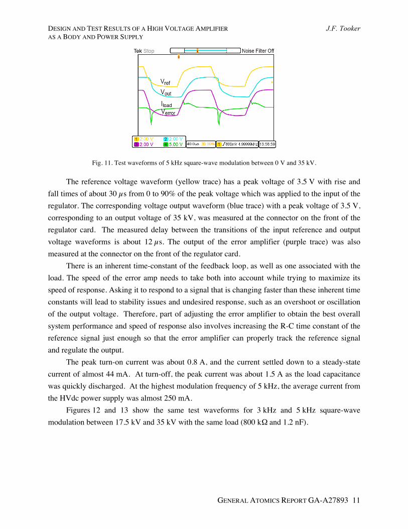
Fig. 11. Test waveforms of 5 kHz square-wave modulation between 0 V and 35 kV.
The reference voltage waveform (yellow trace) has a peak voltage of 3.5 V with rise and fall times of about 30 µs from 0 to 90% of the peak voltage which was applied to the input of the regulator. The corresponding voltage output waveform (blue trace) with a peak voltage of 3.5 V, corresponding to an output voltage of 35 kV, was measured at the connector on the front of the regulator card. The measured delay between the transitions of the input reference and output voltage waveforms is about 12 µs. The output of the error amplifier (purple trace) was also measured at the connector on the front of the regulator card.
There is an inherent time-constant of the feedback loop, as well as one associated with the load. The speed of the error amp needs to take both into account while trying to maximize its speed of response. Asking it to respond to a signal that is changing faster than these inherent time constants will lead to stability issues and undesired response, such as an overshoot or oscillation of the output voltage. Therefore, part of adjusting the error amplifier to obtain the best overall system performance and speed of response also involves increasing the R-C time constant of the reference signal just enough so that the error amplifier can properly track the reference signal and regulate the output.
The peak turn-on current was about 0.8 A, and the current settled down to a steady-state current of almost 44 mA. At turn-off, the peak current was about 1.5 A as the load capacitance was quickly discharged. At the highest modulation frequency of 5 kHz, the average current from the HVdc power supply was almost 250 mA.
Figures 12 and 13 show the same test waveforms for 3 kHz and 5 kHz square-wave modulation between 17.5 kV and 35 kV with the same load (800 kΩΩ and 1.2 nF).

J.F. Tooker DESIGN AND TEST RESULTS OF A HIGH VOLTAGE AMPLIFIER AS A BODY AND POWER SUPPLY
GENERAL ATOMICS REPORT GA-A27893 12
Fig. 12. Test waveforms of 3 kHz square-wave modulation between 17.5 kV and 35 kV.
Fig. 13. Test waveforms of 5 kHz square-wave modulation between 17.5 kV and 35 kV.
Modulation was performed for durations of one hour to measure the stabilized temperature rise of the air flow cooling the transistor modules at different modulation frequencies. For modulation between 35 kV and 0 V at the frequencies of 1 kHz and 2 kHz, the stable temperature rises were 9 and 14 degrees Celsius, respectively. At the modulation frequencies of 3 kHz, 4 kHz, and 5 kHz while modulating the output voltage between 35 kV and 17.5 kV, the stabilized temperature rises were 11, 14, and 16 degrees Celsius, respectively.
The next tests were into the dummy load with the same load resistance of 800 kΩΩ, but with the higher total load capacitance of 3.05 nF (2.35 nF in the dummy load and 0.7 nF from the output coaxial cable). Figures 14, 15, and 16 show the same test waveforms for square-wave modulation between 0 and 35 kV at 100 Hz, 1 kHz, and 5 kHz, respectively. The delay between the transitions of the input reference and output voltage waveforms stayed the same, about 12 µs. However, modulation with the higher load capacitance resulted in higher peak currents at turn-on, about 2 A, and turn-off, about 5 A.

DESIGN AND TEST RESULTS OF A HIGH VOLTAGE AMPLIFIER J.F. Tooker AS A BODY AND POWER SUPPLY
GENERAL ATOMICS REPORT GA-A27893 13
Fig. 14. Test waveforms of 100 Hz square-wave modulation between 0 V and 35 kV with higher load capacitance.
Fig. 15. Test waveforms of 1 kHz square-wave modulation between 0 V and 35 kV with higher load capacitance.
Fig. 16. Test waveforms of 5 kHz square-wave modulation between 0 V and 35 kV with higher load capacitance.

J.F. Tooker DESIGN AND TEST RESULTS OF A HIGH VOLTAGE AMPLIFIER AS A BODY AND POWER SUPPLY
GENERAL ATOMICS REPORT GA-A27893 14
V. SUMMARY The test data has shown successful control of the dc output voltage of the high voltage
amplifier over the full range of output voltage from 0 V to 35 kV and successful square-wave modulation at frequencies up to 5 kHz with load capacitances ranging from 0.7 nF to 3.05 nF. The high voltage amplifier exceeds the requirements for the body power supply of the new 117.5 GHz gyrotron for DIII-D and can meet those of other depressed collector gyrotrons.