design and optimization of a high-performance llc ... · 5-2 topic 5 texas instruments slup30...
TRANSCRIPT

Power Supply Design Seminar
Design and Optimization of a High-Performance LLC Converter
Reproduced from2012 Texas Instruments Power Supply Design Seminar
SEM2000, Topic 5TI Literature Number: SLUP306
© 2012, 2013 Texas Instruments Incorporated
Power Seminar topics and online power- training modules are available at:
ti.com/psds

5-2
Topi
c 5
Texas Instruments SLUP306
Design and Optimization of a High-Performance LLC Converter
Brent McDonald and Dave Freeman
AbstrAct
In this paper, you will learn how to optimize the design of a resonant DC/DC converter using two inductors, LL, and a capacitor, C, known as an LLC converter. Our discussion will include a general background to make the topology easier to understand, a detailed transformer model and characterization procedure, and solutions to several common performance limitations. These solutions are rooted in pulse-width modulation (PWM) control enhancements to optimize performance during startup, short circuit, synchronous rectification and light load.
I. IntroductIon
High efficiency and high-performance power delivery are important to both power-supply design houses as well as the end users of these power supplies [1][7]. In some cases, the total efficiency of the power supply is required to be 96 percent (see Table 1), while simultaneously maintaining a high power factor and low total harmonic distortion [1].
Requirements like this are putting significant pressure on the DC/DC stage to deliver efficiency in excess of 96 percent in order to make up for losses in the power-factor-correction stage.
Resonant LLC converters are receiving significant attention due to their ability to achieve these high efficiencies. Unfortunately, the implementation of many traditional high-performance features are not well understood for this topology. In addition, experience has shown that these features are also more difficult to implement even when they are understood.
In this paper, we will address three problem areas associated with resonant LLC converters – fundamental operation, resonant tank design and pulse-width modulation (PWM) methods for optimized performance – and provide detailed design insight as well as practical solutions to overcome associated challenges.
Topi
c 5
80 PLUS Certification 115-V Internal Nonredundant 230-V Internal Redundant
% of Rated Load 10% 20% 50% 100% 10% 20% 50% 100%
80 PLUS – 80% 80% 80% N/A
80 PLUS Bronze – 82% 85% 82% – 81% 85% 81%
80 PLUS Silver – 85% 88% 85% – 85% 89% 85%
80 PLUS Gold – 87% 90% 87% – 88% 92% 88%
80 PLUS Platinum – 90% 92% 89% – 90% 94% 91%
80 PLUS Titanium – – – – 90% 94% 96% 91% Table 1 – 80 Plus certification requirements.

5-3
Topi
c 5
Texas Instruments SLUP306
II. LLc converter overvIew
Historically, buck-derived topologies have dominated the landscape of high-performance DC/DC converters: topologies include buck, push-pull, forward, half-bridge, full-bridge, phase-shifted full-bridge, etc. These circuits offer an intuitive venue for designers to work in.
Fundamentally, a buck converter works by creating a high-frequency square wave that runs through a low-pass filter to generate a DC output voltage. This low-pass filter usually comprises an inductor and capacitor, creating a classic second-order two-pole rolloff.
Controlling the output voltage is most often achieved by operating this square wave with a constant frequency-variable duty cycle (although other types of control exist). This kind of intuitive converter operation is not as easily extended to an LLC converter, however.
A. Fundamental Operation of an LLC Converter
Let’s start with a brief overview of this converter and its salient operating states. Figure 1
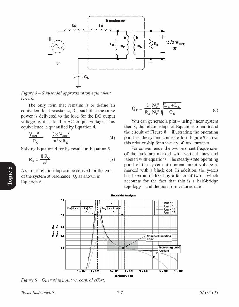
illustrates the basic schematic for a half-bridge LLC power stage as well as the critical operating variables in the system. The output voltage is commonly controlled by using a fixed duty cycle (e.g., 50 percent) and a variable frequency. We’ll discuss this further in section II-C.
Figure 2 illustrates how this system achieves zero voltage-switching (ZVS) on Q1 and Q2. In this figure, both Q1 and Q2 are modeled as ideal switches in parallel with a capacitor and diode. The node connecting Q1 and Q2 is driven by an inductor. This inductor behaves, conceptually, as a current source during the transition time.
State 1 shows that the VDS of Q2 is charged all the way to VIN, with the inductor current flowing through the channel of Q1. When Q1 turns off, the current that was flowing through Q1’s channel diverts and flows through the two capacitors, as shown in state 2. This state continues until the VDS of Q2 has dropped low enough to forward-bias the diode across Q2. At this point operation transitions to state 3. Now the system is free to turn on Q2 with a near zero voltage, thus achieving the so-called ZVS, as shown in state 4.
Figure 1 – Basic LLC schematic.

5-4
Topi
c 5
Texas Instruments SLUP306
B. Piecewise Linear Operating StatesA buck converter has two fundamental
operating modes: continuous conduction mode (CCM) and discontinuous conduction mode (DCM). CCM occurs when the inductor current changes continuously throughout the switching cycle. DCM occurs at light loads when the inductor current is clamped at 0 A, preventing any further reduction in the current.
Critical conduction occurs when the inductor current touches 0 A for an instant; this is the boundary between CCM and DCM. Additional modes are possible based on the type of rectification employed; however, these are the most common.
We can identify similar modes in an LLC converter. Figure 3 shows the operation at the boundary between two of the most common operating modes of the converter. The waveform names match those of Figure 1.
In Figure 2, the input voltage has been varied so that the system control effort (the operating frequency) is exactly equal to the dominant frequency of the resonant tank.
(1)
Figure 3 – Operation at resonance; VIN = 387.6 V.
Notice, at this operating point, ILR(t) and VCR(t) are sine waves; VOUT(t) ripple and ISEC(t) are rectified sine waves, and ILM(t) is a triangle wave. This represents the simplest operating mode of the converter.
Figure 2 – Zero voltage switching.

5-5
Topi
c 5
Texas Instruments SLUP306
The input voltage is now increased so that the system control effort changes the frequency to something above resonance.
(3)
Figure 5 illustrates the waveforms for the condition of Equation 3. More distortion is now present in the waveforms, making the sinusoidal characteristics less pronounced. In this case, the primary MOSFETs Q1 and Q2 are switched before ILR(t) is equal to ILM(t). This does not affect the ZVS on Q1 and Q2; however, it does change the switching characteristics of Q3 and Q4.
In Figures 3 and 4, notice that the current through Q3 and Q4 naturally decays to 0 A, providing zero current switching (ZCS) for these devices. In this case, switching Q1 and Q2 – prior to Q3 and Q4 reaching zero current – results in the loss of ZCS for these devices.
Figure 4 – Operation below resonance; VIN = 370 V.
To visualize this, recognize that Q1 and Q2 generate a square wave at the input to LR. This square wave is filtered to produce a sine wave in ILR(t). The voltages across LR + LK and CR are 180 degrees out of phase and equal and opposite in magnitude. These voltages cancel out one another and produce a square wave voltage across LM. This square wave produces the triangular-shaped current ILM(t) shown in Figure 3.
The input voltage is now reduced so that the system control effort changes the frequency to something below the resonant frequency, as defined by Equation 2.
(2)
Figure 4 illustrates the waveforms for the condition of Equation 2. Most of the sinusoidal nature of the waveforms in Figure 3 are preserved; the exception to this is introduced by the dead time between the conduction of Q3 and Q4 as shown by ISEC(t). This dead time is produced when ILR(t) becomes equal to ILM(t), reducing the order of the tank by one.
Figure 5 – Operating above resonance; VIN = 410 V.

5-6
Topi
c 5
Texas Instruments SLUP306
C. Sinusoidal ApproximationWe can simplify this concept significantly by
exploiting the sinusoidal nature of the system waveforms. Figure 6 shows the same schematic as Figure 1, but with the addition of two labeled variables.
Figure 7 plots what these waveforms look like when operation is at resonance, as defined by Equation 1 and Figure 3. Assuming that the bulk of the energy is transferred through the fundamental components of these square waves, these waveforms can be simplified to the sinusoidal curves overlaid on each plot in Figure 7.
You can calculate the amplitude of these sine waves using a Fourier series expansion with the closed form result shown in the legend entry for each plot in Figure 7. Utilizing these sinusoidal relationships and the RMS values of these signals results in the simplified schematic shown in Figure 8.
Figure 6 – Sinusoidal approximation schematic.
Figure 7 – Sinusoidal approximation assumptions.
5-7
Topi
c 5
Texas Instruments SLUP306
(6)
You can generate a plot – using linear system theory, the relationships of Equations 5 and 6 and the circuit of Figure 8 – illustrating the operating point vs. the system control effort. Figure 9 shows this relationship for a variety of load currents.
For convenience, the two resonant frequencies of the tank are marked with vertical lines and labeled with equations. The steady-state operating point of the system at nominal input voltage is marked with a black dot. In addition, the y-axis has been normalized by a factor of two – which accounts for the fact that this is a half-bridge topology – and the transformer turns ratio.
The only item that remains is to define an equivalent load resistance, RE, such that the same power is delivered to the load for the DC output voltage as it is for the AC output voltage. This equivalence is quantified by Equation 4.
(4)
Solving Equation 4 for RE results in Equation 5.
(5)
A similar relationship can be derived for the gain of the system at resonance, Q, as shown in Equation 6.
Figure 8 – Sinusoidal approximation equivalent circuit.
Figure 9 – Operating point vs. control effort.

5-8
Topi
c 5
Texas Instruments SLUP306
Figure 11 – Leakage-inductance model.
If you were to plot this same relationship for a buck-derived topology operating in CCM, the x-axis control effort would be replaced with duty cycle and the first-order curve would simply be a straight line independent of load. The LLC case is quite different. The curves are load-dependent and non-monotonic. Under normal circumstances, a non-monotonic relationship like this is disastrous for a control loop. You can address this by constraining the operating frequency to a range where the curves are monotonic, as shown by the gray box. The boundary conditions for this box are chosen based on the required operating points of the system (such as what output and input voltages are required) and the component operational limits (switching losses and volt-second limits on transformers, for example).
This method is an extremely useful approximation for determining the DC operating point near the resonant frequency. As the operation deviates from this frequency, more error is introduced into the approximation. Yet this method is still useful as a starting point for the design and provides considerable insight into operation at many different frequencies.
Time-domain simulation is required for more accurate results, however, and the method provides no insight into the small-signal behavior of the system. Reference [2] provides extensive details on how to apply and use this method to the design of LLC converters.
III. trAnsformer modeLIng And desIgn
At the heart of the LLC converter is the resonant tank, and central to the resonant tank is the transformer itself. In order to properly utilize this topology, it is of utmost importance to have a transformer model that preserves the salient features of the converter operation. Such a model needs to capture the significant AC and DC system operating characteristics and should also be easy to characterize and use. In this section, we’ll present just such a model and discuss the design impacts to the LLC converter.
A. Previous ModelsFigure 10 shows the schematic for the classic
mutual-inductance coupled-inductor model.
Equations 7 and 8 exactly describe the behavior of this model.
(7)
(8)
Mathematically, this model can be easily extended to any number of windings; however, it is very mathematically oriented and thus it is difficult to derive any intuition from it. A better alternative is the so-called leakage-inductance model shown in Figure 11.
Figure 10 – Mutual inductance model.
5-9
Topi
c 5
Texas Instruments SLUP306
Using Equations 9 to 12, you can see an exact equivalence between the mutual-inductance model and the leakage-inductance model.
(9)
(10)
(11)
(12)
The parameters of the leakage-inductance model are easy to measure, with conventional lab equipment making it easy to characterize. This simplicity also brings with it considerable physical insight to both transformer construction and behavior.
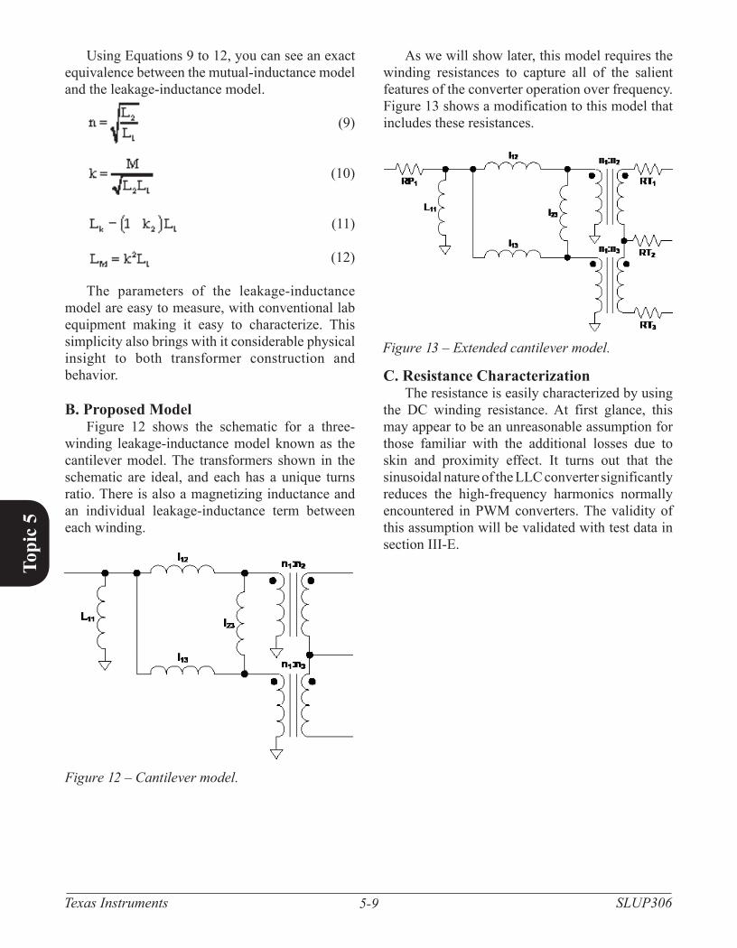
B. Proposed ModelFigure 12 shows the schematic for a three-
winding leakage-inductance model known as the cantilever model. The transformers shown in the schematic are ideal, and each has a unique turns ratio. There is also a magnetizing inductance and an individual leakage-inductance term between each winding.
Figure 12 – Cantilever model.
As we will show later, this model requires the winding resistances to capture all of the salient features of the converter operation over frequency. Figure 13 shows a modification to this model that includes these resistances.
C. Resistance CharacterizationThe resistance is easily characterized by using
the DC winding resistance. At first glance, this may appear to be an unreasonable assumption for those familiar with the additional losses due to skin and proximity effect. It turns out that the sinusoidal nature of the LLC converter significantly reduces the high-frequency harmonics normally encountered in PWM converters. The validity of this assumption will be validated with test data in section III-E.
Figure 13 – Extended cantilever model.

5-10
Topi
c 5
Texas Instruments SLUP306
Figure 14 illustrates a series of measurements that can easily characterize the DC resistance terms of the model of Figure 13. In each case, the current source represents a precision resistance meter.
You can use Equations 13, 14 and 15 to easily convert these values to the model parameters shown in Figure 13.
(13)
(14)
(15)
D. Inductance CharacterizationWe will cover two methods for characterizing
model-inductance parameters. The direct method offers a mathematically simple solution at the expense of more complex measurement methods. In contrast, the indirect method is mathematically complex; however, the measurements are intuitive, accurate and easy to perform.
i. Direct Method
Figure 14 – Resistance characterization.
Figure 15 – Direct measurement method.
Figure 15 illustrates the measurement of l12. In this case, both tertiary windings are shorted, a voltage stimulus is applied to the primary, and the resulting current is measured on the n2 winding. If the shorts applied to the tertiary windings are sufficiently low to guarantee that no current flows through l23, then the measurement of iac will be equal to the current through l12 transformed by turns ratio. Mathematically, this is expressed as Equation 16.
(16)
You can follow a similar procedure to obtain measurements for l13 and l23, resulting in Equations 17 and 18.
(17)
(18)
Although mathematically and conceptually simple, the practical implementation of accurate measurements is difficult. First, conventional impedance analyzers are constructed to inject and measure at the same node. But in this case, the injection node and one of the measurement nodes occurs at the same place, while the current measurement occurs at a remote location. While this is technically feasible, it is not convenient. In
5-11
Topi
c 5
Texas Instruments SLUP306
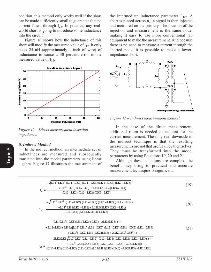
the intermediate inductance parameter LK2. A short is placed across n2; a signal is then injected and measured on the primary. The location of the injection and measurement is the same node, making it easy to use more conventional lab equipment to make the measurement. And because there is no need to measure a current through the shorted node, it is possible to make a lower-impedance short.
In the case of the direct measurement, additional room is needed to account for the current measurement. The only real downside of the indirect technique is that the resulting measurements are not that useful all by themselves. They must be transformed into the model parameters by using Equations 19, 20 and 21.
Although these equations are complex, the benefit they bring to practical and accurate measurement techniques is significant.
(19)
(20)
(21)
addition, this method only works well if the short can be made sufficiently small to guarantee that no current flows through l23. In practice, any real-world short is going to introduce some inductance into the circuit.
Figure 16 shows how the inductance of this short will modify the measured value of l12. It only takes 25 nH (approximately 1 inch of wire) of inductance to cause a 30 percent error in the measured value of l12.
ii. Indirect MethodIn the indirect method, an intermediate set of
inductances are measured and subsequently translated into the model parameters using linear algebra. Figure 17 illustrates the measurement of
Figure 16 – Direct measurement insertion impedance.
Figure 17 – Indirect measurement method.
5-12
Topi
c 5
Texas Instruments SLUP306
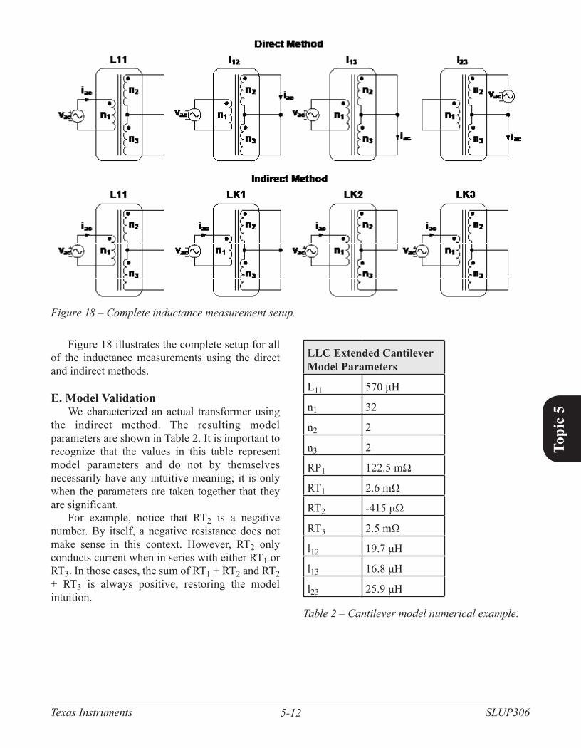
Figure 18 illustrates the complete setup for all of the inductance measurements using the direct and indirect methods.
E. Model ValidationWe characterized an actual transformer using
the indirect method. The resulting model parameters are shown in Table 2. It is important to recognize that the values in this table represent model parameters and do not by themselves necessarily have any intuitive meaning; it is only when the parameters are taken together that they are significant.
For example, notice that RT2 is a negative number. By itself, a negative resistance does not make sense in this context. However, RT2 only conducts current when in series with either RT1 or RT3. In those cases, the sum of RT1 + RT2 and RT2 + RT3 is always positive, restoring the model intuition.
Figure 18 – Complete inductance measurement setup.
LLC Extended Cantilever Model Parameters
L11 570 μH
n1 32
n2 2
n3 2
RP1 122.5 mΩ
RT1 2.6 mΩ
RT2 -415 μΩ
RT3 2.5 mΩ
l12 19.7 μH
l13 16.8 μH
l23 25.9 μH
Table 2 – Cantilever model numerical example.

5-13
Topi
c 5
Texas Instruments SLUP306
Figure 19 – Model results vs. measurement.
Figure 20 – Measurement and model results with capacitance.
Figure 19 shows the measured results of the indirect method compared to the model. The plots on the left are the various inductance impedance measurements, while the plots on the right are the effective primary to secondary turns ratios.
In general the correlation is very good; however, there is one obvious discrepancy: the resonance at ~300 kHz. This is the result of the parasitic capacitance of the transformer in parallel with the capacitance of the measurement probes. This capacitance is estimated – via a curve fit – and included in the model plot in Figure 20.
The remaining poles and zeros in the plots of Figure 19 are due to the interaction of the inductance and resistance terms. In the previous section, the model resistances were characterized using the DC assumption. Given the very close correlation between model and measurement over a wide frequency range in Figure 19, this assumption appears well-justified.

5-14
Topi
c 5
Texas Instruments SLUP306
F. Design ImpactsGiven the need for a series-inductance term in
the LLC converter to regulate the output, it is generally acknowledged that some primary to secondary leakage inductance is beneficial to the system. In fact, if this inductance is properly sized, it can even eliminate the need for an external inductor.
Although this leakage term is valuable, leakage between the tertiary windings can be problematic to the design. Adverse effects can be introduced that compromise power-supply performance, including higher-voltage synchronous rectifiers, increased RMS currents, larger-output ripple voltage, and the potential to alter the steady-state and small-signal operating characteristics.
Figure 21 illustrates part of the impact of this leakage. The plots on the left show the resonant inductor current and the output voltage ripple for the transformer characterized by the data in Table 2. In general, the waveforms are very symmetric, having minimal ripple and RMS current values. The plots on the right show the results with an additional 75 nH of inductance introduced between the two tertiary windings. This inductance increases the output ripple voltage by approximately 10 percent.
We can make several additional observations directly from the model shown previously in Figure 13.
•
– No additional synchronous rectifier stress– Everything is symmetrical – minimal ripple and RMS currents
•
– Synchronous rectifier voltage stresses can still be significant– Everything is symmetrical – minimal ripple and RMS currents
•
– Maximum stress on the synchronous rectifiers– Ripple
• l12 = l13, symmetrical – minimal ripple and RMS currents
• l12 > l13, asymmetrical
• l12 < l13, asymmetrical
Figure 21 – Large-signal impact of leakage.
5-15
Topi
c 5
Texas Instruments SLUP306
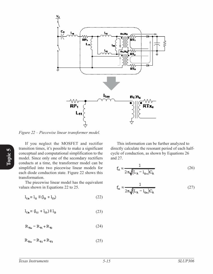
If you neglect the MOSFET and rectifier transition times, it’s possible to make a significant conceptual and computational simplification to the model. Since only one of the secondary rectifiers conducts at a time, the transformer model can be simplified into two piecewise linear models for each diode conduction state. Figure 22 shows this transformation.
The piecewise linear model has the equivalent values shown in Equations 22 to 25.
(22)
(23)
(24)
(25)
Figure 22 – Piecewise linear transformer model.
This information can be further analyzed to directly calculate the resonant period of each half-cycle of conduction, as shown by Equations 26 and 27.
(26)
(27)

5-16
Topi
c 5
Texas Instruments SLUP306
G. Design ConsiderationsAs a final step in the transformer analysis, you
must consider how these leakage inductances function relative to winding placement. Figure 23 shows a simple transformer bobbin and cross-section. In this example, the primary is constructed of round copper wire in the center of the structure. There are two tertiary windings constructed of copper foil. In all cases, each individual wire represents a single turn on the transformer.
To the right of the bobbin and wire cross-section is an expanded view of the transformer
windings while conducting current. A dot indicates that current is flowing out of the page, while an “x” indicates that current is flowing into the page. In this example, the dark gray tertiary is conducting.
The magnetomotive force (MMF) drawing in the upper-right corner illustrates the leakage inductance that exists between layers. This plot is generated by drawing a box that starts in the center of the windings and expands outward. The sum of the current inside of this box is equal to the MMF at that particular location.
Figure 23 – Transformer winding analysis.

5-17
Topi
c 5
Texas Instruments SLUP306
Figure 24 applies this same analysis to three different interleaving strategies for conduction in both T1 and T2. When the windings are fully interleaved, the area under the MMF functions is minimized. It is also important to note that the MMF levels are not the same when T1 conducts versus T2. Minimizing the MMF results in lower leakage and reduced losses due to proximity effect.
Iv. Pwm methods for oPtImIzed PerformAnce
A. Problem No. 1: High fsWhile an LLC converter offers a variety of
advantages, there are several performance features that are more difficult to achieve than when
designing with its buck-derived counterparts. First, requirements for light load, high input voltage or low output voltage require the converter to operate at high switching frequencies (see Figure 9 for details). These operating points can introduce additional switching losses; introduce regulation problems [5]; make soft start difficult; and even prevent operation in constant current, constant power or short circuit.
The fundamentals of steady-state operation were covered in section II-A. In this context, Figure 25 illustrates the exact timing relationships between the primary-side MOSFET control signals and the synchronous-rectifier control signals.
Figure 24 – Transformer winding strategy.

5-18
Topi
c 5
Texas Instruments SLUP306
As an alternative to continuing to raise the switching frequency, it is possible to seamlessly switch modulation from frequency to pulse width. The PWM control signals are shown in Figure 26.
Notice that when the FM control frequency is equal to the PWM frequency, these waveforms are identical. This facilitates a perfectly smooth handoff between FM and PWM operation. Figure 27 illustrates this handoff during a typically soft start cycle. Notice the smooth, monotonic output voltage through the entire operation.
Figure 25 – Frequency modulation.
Figure 26 – Pulse-width modulation.
Figure 27 – Soft start.

5-19
Topi
c 5
Texas Instruments SLUP306
As another example, consider overload operation where the control transitions from constant voltage to constant power and constant current. Figure 28 shows the measured output voltage of the converter as it transitions through these three operating regions.
B. Problem No. 2: Synchronous Rectification
A second challenge is synchronous rectification. The timing of a properly diode-emulated synchronous rectifier does not follow the primary
Figure 28 – Constant current constant power.
MOSFET control signal. Traditionally, you can solve this problem by using some kind of current-sensing circuitry to determine when the synchronous rectifier should be on and off. As an alternative, a programmable pulse-width clamp is placed on the synchronous-rectifier pulse width. If the width of this pulse is approximately equal to one-half the natural resonant period, you will get a very good approximation of an emulated diode. Figures 29 and 30 illustrate this relationship for a variety of input-voltage and load-current conditions.
Figure 29 – Synchronous rectifier current and input voltage.

5-20
Topi
c 5
Texas Instruments SLUP306
Figure 30 – Synchronous rectifier current and load current.
Figure 31 illustrates the MOSFET control signals for this operating mode. The synchronous rectifiers simply follow the primary MOSFET signal (minus dead times) until the pulse width is longer than the preprogrammed clamp value. Once this happens, frequency adjustments continue to occur on all channels; however, only the primary MOSFET control signals maintain their duty-cycle ratio of ~50 percent.
Figure 31 – Synchronous rectifier clamp mode.
5-21
Topi
c 5
Texas Instruments SLUP306
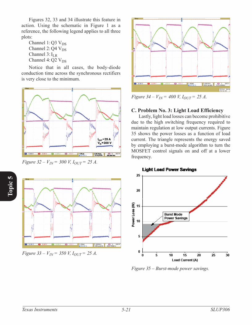
C. Problem No. 3: Light Load Efficiency Lastly, light load losses can become prohibitive
due to the high switching frequency required to maintain regulation at low output currents. Figure 35 shows the power losses as a function of load current. The triangle represents the energy saved by employing a burst-mode algorithm to turn the MOSFET control signals on and off at a lower frequency.
Figure 32 – VIN = 300 V, IOUT = 25 A.
Figure 33 – VIN = 350 V, IOUT = 25 A.
Figure 34 – VIN = 400 V, IOUT = 25 A.
Figure 35 – Burst-mode power savings.
Figures 32, 33 and 34 illustrate this feature in action. Using the schematic in Figure 1 as a reference, the following legend applies to all three plots:
Channel 1: Q3 VDSChannel 2: Q4 VDSChannel 3: ILRChannel 4: Q2 VDS
Notice that in all cases, the body-diode conduction time across the synchronous rectifiers is very close to the minimum.

5-22
Topi
c 5
Texas Instruments SLUP306
Figure 36 illustrates the algorithm. The compensator control effort is used as a crude indication of the load current. When this signal drops below a programmed threshold (labeled “Turn Off Threshold”), all of the MOSFET control signals are turned off. When it rises above a
second programmed threshold (labeled “Turn On Threshold”), they turn on again.
Since the compensator control effort is only a crude representation of the load, some additional adjustment of the on/off thresholds is necessary as the input voltage varies.
Figure 36 – Burst-mode algorithm
v. concLusIon
Figure 37 shows a picture of the completed evaluation module (EVM), while Figure 38 shows the corresponding efficiency of this converter.
This EVM incorporates all of the features described in this paper, enabling a solution that provides competitive efficiency while maintaining the classic high-performance features designers are accustomed to using in buck-derived topologies.
Figure 37 – LLC EVM.
The heart of this system uses a Texas Instruments UCD3138 digital controller. This facilitated easy optimization and evaluation of the various control features discussed in Section IV. The digital core of the UCD3138 also provided an efficient solution to the mode-switching problems while maintaining a minimum component count.
Figure 38 – LLC EVM efficiency.
5-23
Topi
c 5
Texas Instruments SLUP306
vI. references
[1] 80 PLUS Certified Power Supplies and Manufacturers. Accessed May 10, 2012. http://www.plugloadsolutions.com/80PlusPowerSupplies.aspx.
[2] Huang, Hong. “Designing an LLC Resonant Half-Bridge Power Converter.” TI Power Supply Design Seminar SEM1900, 2010.
[3] Lu, Bing, Wenduo Liu, Yan Liang, F.C. Lee, and J.D. van Wyk. “Optimal Design Methodology for LLC Resonant Converter.” Paper presented at Applied Power Electronics Conference and Exposition (APEC) 2006, March 19-23, 2006.
[4] Liu, Ya. “High Efficiency Optimization of LLC Resonant Converter for Wide Load Range.” Master’s thesis, Virginia Polytechnic Institute and State University, 2007.
[5] Ye, Yiqing, Chao Yan, Jianhong Zeng, and Jianping Ying. “A Novel Light Load Solution for LLC Series Resonant Converter.” Paper presented at Telecommunications Energy Conference (INTELEC) 2007, September 30-October 4, 2007.
[6] Maksimovic, D., R.W. Erickson, and C. Griesbach. “Modeling of Cross-Regulation in Converters Containing Coupled Inductors.” Paper presented at Applied Power Electronics Conference and Exposition (APEC) 1998, February 15-19, 1998.
[7] Suntio, T., A. Glad, and P. Waltari. “Constant-Current vs. Constant-Power Protected Rectifier as a DC UPS System’s Building Block.” Paper presented at Telecommunications Energy Conference (INTELEC) 1996, October 6-10, 1996.
[8] Lazar, J.F., and R. Martinelli. “Steady-State Analysis of the LLC Series Resonant Converter.” Paper presented at Applied Power Electronics Conference and Exposition (APEC) 2001, March 4-8, 2001.
[9] Synopsys Saber platform. Accessed May 10, 2012. http://www.synopsys.com/Systems/Saber/Pages/default.aspx.
[10] EMA Design Automation Cadence OrCAD 16.5 Lite Software. Accessed May 10, 2012. http://www.ema-eda.com/products/orcad/demosoftware.aspx?campaignID=254&gclid
=CNLT0_Xp86cCFUJm7AoddW2UcQ.[11] SIMetrix Technologies Power Circuit
Simulation. Accessed May 10, 2012. http://www.simetrix.co.uk/site/products/simplis.htm.

TI Worldwide Technical Support
InternetTI Semiconductor Product Information Center Home Pagesupport.ti.com
TI E2E™ Community Home Pagee2e.ti.com
Product Information CentersAmericas Phone +1(512) 434-1560
Brazil Phone 0800-891-2616
Mexico Phone 0800-670-7544
Fax +1(972) 927-6377 Internet/Email support.ti.com/sc/pic/americas.htm
Europe, Middle East, and AfricaPhone European Free Call 00800-ASK-TEXAS (00800 275 83927) International +49 (0) 8161 80 2121 Russian Support +7 (4) 95 98 10 701
Note: The European Free Call (Toll Free) number is not active in all countries. If you have technical difficulty calling the free call number, please use the international number above.
Fax +(49) (0) 8161 80 2045Internet www.ti.com/asktexasDirect Email [email protected]
JapanPhone Domestic 0120-92-3326
Fax International +81-3-3344-5317 Domestic 0120-81-0036
Internet/Email International support.ti.com/sc/pic/japan.htm Domestic www.tij.co.jp/pic
AsiaPhone International +91-80-41381665 Domestic Toll-Free Number Note: Toll-free numbers do not support
mobile and IP phones. Australia 1-800-999-084 China 800-820-8682 Hong Kong 800-96-5941 India 1-800-425-7888 Indonesia 001-803-8861-1006 Korea 080-551-2804 Malaysia 1-800-80-3973 New Zealand 0800-446-934 Philippines 1-800-765-7404 Singapore 800-886-1028 Taiwan 0800-006800 Thailand 001-800-886-0010Fax +8621-23073686Email [email protected] or [email protected] support.ti.com/sc/pic/asia.htm
A090712
Important Notice: The products and services of Texas Instruments Incorporated and its subsidiaries described herein are sold subject to TI’s standard terms and conditions of sale. Customers are advised to obtain the most current and complete information about TI products and services before placing orders. TI assumes no liability for applications assistance, customer’s applications or product designs, software performance, or infringement of patents. The publication of information regarding any other company’s products or services does not constitute TI’s approval, warranty or endorsement thereof.
© 2013 Texas Instruments IncorporatedPrinted in U.S.A. by (Printer, City, State)
The platform bar and E2E are trademarks of Texas Instruments. All other trademarks are the property of their respective owners.
SLUP306

IMPORTANT NOTICE
Texas Instruments Incorporated and its subsidiaries (TI) reserve the right to make corrections, enhancements, improvements and otherchanges to its semiconductor products and services per JESD46, latest issue, and to discontinue any product or service per JESD48, latestissue. Buyers should obtain the latest relevant information before placing orders and should verify that such information is current andcomplete. All semiconductor products (also referred to herein as “components”) are sold subject to TI’s terms and conditions of salesupplied at the time of order acknowledgment.
TI warrants performance of its components to the specifications applicable at the time of sale, in accordance with the warranty in TI’s termsand conditions of sale of semiconductor products. Testing and other quality control techniques are used to the extent TI deems necessaryto support this warranty. Except where mandated by applicable law, testing of all parameters of each component is not necessarilyperformed.
TI assumes no liability for applications assistance or the design of Buyers’ products. Buyers are responsible for their products andapplications using TI components. To minimize the risks associated with Buyers’ products and applications, Buyers should provideadequate design and operating safeguards.
TI does not warrant or represent that any license, either express or implied, is granted under any patent right, copyright, mask work right, orother intellectual property right relating to any combination, machine, or process in which TI components or services are used. Informationpublished by TI regarding third-party products or services does not constitute a license to use such products or services or a warranty orendorsement thereof. Use of such information may require a license from a third party under the patents or other intellectual property of thethird party, or a license from TI under the patents or other intellectual property of TI.
Reproduction of significant portions of TI information in TI data books or data sheets is permissible only if reproduction is without alterationand is accompanied by all associated warranties, conditions, limitations, and notices. TI is not responsible or liable for such altereddocumentation. Information of third parties may be subject to additional restrictions.
Resale of TI components or services with statements different from or beyond the parameters stated by TI for that component or servicevoids all express and any implied warranties for the associated TI component or service and is an unfair and deceptive business practice.TI is not responsible or liable for any such statements.
Buyer acknowledges and agrees that it is solely responsible for compliance with all legal, regulatory and safety-related requirementsconcerning its products, and any use of TI components in its applications, notwithstanding any applications-related information or supportthat may be provided by TI. Buyer represents and agrees that it has all the necessary expertise to create and implement safeguards whichanticipate dangerous consequences of failures, monitor failures and their consequences, lessen the likelihood of failures that might causeharm and take appropriate remedial actions. Buyer will fully indemnify TI and its representatives against any damages arising out of the useof any TI components in safety-critical applications.
In some cases, TI components may be promoted specifically to facilitate safety-related applications. With such components, TI’s goal is tohelp enable customers to design and create their own end-product solutions that meet applicable functional safety standards andrequirements. Nonetheless, such components are subject to these terms.
No TI components are authorized for use in FDA Class III (or similar life-critical medical equipment) unless authorized officers of the partieshave executed a special agreement specifically governing such use.
Only those TI components which TI has specifically designated as military grade or “enhanced plastic” are designed and intended for use inmilitary/aerospace applications or environments. Buyer acknowledges and agrees that any military or aerospace use of TI componentswhich have not been so designated is solely at the Buyer's risk, and that Buyer is solely responsible for compliance with all legal andregulatory requirements in connection with such use.
TI has specifically designated certain components as meeting ISO/TS16949 requirements, mainly for automotive use. In any case of use ofnon-designated products, TI will not be responsible for any failure to meet ISO/TS16949.
Products Applications
Audio www.ti.com/audio Automotive and Transportation www.ti.com/automotive
Amplifiers amplifier.ti.com Communications and Telecom www.ti.com/communications
Data Converters dataconverter.ti.com Computers and Peripherals www.ti.com/computers
DLP® Products www.dlp.com Consumer Electronics www.ti.com/consumer-apps
DSP dsp.ti.com Energy and Lighting www.ti.com/energy
Clocks and Timers www.ti.com/clocks Industrial www.ti.com/industrial
Interface interface.ti.com Medical www.ti.com/medical
Logic logic.ti.com Security www.ti.com/security
Power Mgmt power.ti.com Space, Avionics and Defense www.ti.com/space-avionics-defense
Microcontrollers microcontroller.ti.com Video and Imaging www.ti.com/video
RFID www.ti-rfid.com
OMAP Applications Processors www.ti.com/omap TI E2E Community e2e.ti.com
Wireless Connectivity www.ti.com/wirelessconnectivity
Mailing Address: Texas Instruments, Post Office Box 655303, Dallas, Texas 75265Copyright © 2013, Texas Instruments Incorporated