design and modeling of deep-submicrometer mosfets … · october 2,1990 . design and modeling ......
TRANSCRIPT

DESIGN AND MODELING OF DEEP-SUBMICROMETER MOSFETS
by
Min-Ch ie Jeng
Memorandum No. UCB/ERL M90190
October 2,1990


DESIGN AND MODELING OF DEEP-SUBMICROMETER MOSFETS
by
Min-Chie Jeng
Memorandum No. UCBERL M90/90
2 October 1990
ELECTRONICS RESEARCH LABORATORY
College of Engineering University of California, Berkeley
94720


i
PhcD
Design and Modeling of Deep-Submicrometer MOSFETs
Min-Chie Jeng
ABSTRACT
A photoresist ashing technique has been developed which, when used in conjunction with
conventional optical lithography, permits controlled definition of the gate of deep
submicrometer MOSFETs. 'Ihis technique can also be extended to other lithographic
processes, such as e - b and x-ray. Comprehensive studies based on the pedormance and
hotelectron reliability hwe shown that the basic physics d a t e d with deepsubmi-
devices is similar to that of their longer<hannel mmkprts. 'Iherefoxe, existing device
design guidelines and models can sti l l be used with minor modifications. A set of design
curves has been generated based on experimental d t s With various mechauisms under COD
sideration. With these design curves, the t r & d € s between dewice dimensions and power sup
ply for a particular technology am be cbsemed. 'Ihe relative importance of each mechaaism
can also be identified.
A semi-empirical MOSFET drain cwrent model BcwBtc down to quarter-micron than-
eels, suitable for digital as well LIS analog qqAidons has been developed. Both the drain
currenf and the output reshnce am accurately modeled. 'Ihe first derivative of the drain
ament equation is Continuous hm the subthreshold region to the Strong-iWerSiOn region and
from the linear region to the s a t u d o n region. for dl biases. 'Ibis model has bea implb
mented in SpIcE3. A parameter extraction system dedicated to the model was also developed.

ii

iii
ACKNOWLEDGEMENTS
Fm of all, I would like to express my deepest apprcciarions to my ltseaTch advisor Prof.
Ping K. KO. This dissertation would not have been possible without his guidance and support.
I also would like to thank my ca-advisor Prof. Chcnming Hu for his helpful discussion
and valuable comments throughout this wok
I would like to thank Prof. Charles I. Stone of Statistics Departmau for W i g a member
of my qualifying exam and for providing me basic statistical background which is very helpful
in extracting model parameters in this work
I would like to thank Prof. David A. Hodges for his continuous encouragement and sup
port of the BSIM project
I am grateful to Prof. Sing J. Sku of USC and Tony Fung for their kind help in the
early stage of this work. I thank Dr. Albert T. Wu, James Chung, James E. Moon, Kataline
Voros, Marilyn Kushner, Robin R Rude& and Tom Booth for -their assistaaCe in fabricating
deepsubmicrometer devices.
I also would like to thank my officemate, P e r M. Lee and Jon S. Duster, for providing
me a friendly working environment and for proofreading this dissertation. I really enjoyed
working with them.
Finally, I am indebted to my parents who always provide me strtngth and faith at the
right time, and my beloved wife, Ya-Lte, for hex patience and sacrifice during my graduate
study at Berkeley.
This research was funded by the Semiconductor Research Corporation, the California
State MICRO program and JSEP under contract F49620-84-c-0067.


V
Table of Contents
Chapter 1: INTRODUCTION .. ................ .........................”................ .............L.......-.. 1
1.1. design n ... n........n........n.........n..-...n...n...n...n...n....n...n...n...n...”..-..-.. 2
12 . Device mod$ing ” ......................... ............................................................... 4
5
7
13 . atl ine .................... ” ........................ ....... ............................. ” .................. .........-. 1.4. References .................................................................. .. ....................................... ....
Chapter 2: DEVICE FABRICATION ....... .................................................................... 11
11 2.1. Fabrication process ........................................................................................ ......... 2 2 . Photoresist-ashing technique .......................................................................... .........
22.1. Wder p”p”ati0a ................................................ .. .................................. U ... ”.. 2 2 2 . EtchiDg process .......................... .....................................................................
2 2 3 l3primataI results ...._.............. .. .............................................................. ..... 23 . Device chamAenstics ....................................... .. ................................................. .. 2.4. References ............... ............. ....... .... ... . ._ ....................................... .. ..... ....... ..........
Chapter 3: PERFORMANCE AND HOT-ELECTRON RELIABILITY OF
DEEP-SUBMICROMETER M O M .................... ............. .. .............. ............. .........
3 2 2 . Subthreshold swing .............. .. .... ....... ............... ... ” .................................. ......... 3 3 . CmeQt driving capability ..... ..................................................................................
12
14
14
15
23
27
28
29
37
28
48
48

vi
Chapter 4: DEEP-SUBMICROMETER MOSFET DESIGN ........................................ 4.1. Device limitations .................. .. ........................................................... .. .................
4.1.1. 'Ihreshold voltage shift ......................... .. ......................................................... 4.1 2 . a-state leakage CUUW ................. n ............................................. n...-...n..
4.13. Hotelectron reliability ............... ....... ........ .. ........ ....... ..... : ............. ................... 4.1.4. Breakdown voltcrge ............................... n ... n...-........-...................n...-...-...n.. 4.15. Tidependent-clieldc b r e a k h ...................... .. ............................. .. .......
4 2 . Performance constraints ....................................................................... . ................. 42.1. Chrrat-driviqg capability ............... ....... ........ ............ ................... ................... 4 2 2 . Voltage gain .. .................. ....... .... .. ........ ................. .................................. ......... 4 2 3 . swi* speed ..............-.. n ................... n ............................ n ............. W .......
4 3 . W i n g u i & h .............. .. ........ .. .............. ....... ............. .. .............. ...................... .H
43.1. t h i c k vusus c h d length .n ... n...n...-...a...................n........-...- 4 3 2 . Power supply versus channd leagth .... ..................... .............. .. ........ .. ........ .... 4 3 3 . Power supply vezsus oxide thickness ... .. ................................................. " ....... 43.4. Junction depth ............ " ................................................................ .. ............. .... .
52
52
53
58
61
61
69
73
79
80
80
80
85
85
85
89
89
89
89
94
95
97
97
97

4 3 5 . OttKt puwa Supply and devioe dmadoas ....... 43.6 other techwlogies .......................... .................-................... ..............
- ........................ 100
100
4.4. RefCnaas ................................................................................................. 102
Chapter 5: A DEEP-SUBMICROMETER MOSFE3I' MODEL FOR
ANALOGDIGITAL CIRCUIT SIMULATIONS .... " ........ ..... ................ ..... ................... 104
5.1. General properties of MOSFET modcliqg ...................................... .. ................-.. 105
5.1.1. Semi-emphkaI nature .................................................... " ............................ ".. 105 5.12. Accuracy ................................................................. " ................... n........"...n.. 105
5.13. compltational efficiency .................................................................... .. ........ .... 106
L
5.1.4. Ease of parameter extraction ................................................................. " ... ".. 52 . BSIM . Berkeaq Short-chmd IcaFm Model ..... " ....................................... " ... ".. 52.1. ?he BSIM agpIoach ....................................... .. ....................................... ......... 522 . BSTMl revim ....... .. .................................. " ............. ........................ .....".......
53 . ?he BSIM;! moQl .............. ....................................... .. ............................. .............. 53.1. Physical effects included ................................ .. ........ .. ............................. ......... 532 . Strong-inversion region .................................................................................... 533 . Subthreshold region ................................... .. ............. ................................. ... ..
106
107
107
107
110
110
113
128
53.4. Transition e o n ........................ ....... ...................................................... .....".. 130
535 . c)utpt resistance modeling .......................................................... " ........ "...".. 137
53.6. Biasdependeat paremerers ......... .. .................. " ............................. .. ............._.. 148
53.7. S h i n d e p d e a t pammtas ........................................................................ " .. 149
5.4. Parameter extraction for WIM2 ...................... .................................. " ........ .....".. 151
5.4.1. Automated parameter extraction system .... .. ............. .. .................................. " .. 151
5.42. @orithaas ." ............................. n.......................................n...n..-.. 152

Chapter 1
INTRODUCTION
In the last decade, MOS devices have been miniamid to acbieve higher packing derp
sity, higher integration levels, and higher current drive. Recent advances in process technology
(1.1-1.71 have made deepsubmicrometer MOSFETs potential candidares for next generation
ULSI designs. However, by demasing channel length while maintaining the current power
supply voltage, the electric fields in the device will m e r increase, causing the device charac-
teristics to deviate from the long-channel behavior and also creating reliability problems.
The two high-field effects most pronounced on device performance are the mobility
degradation due to vertical-field [1.8-1.111 and the carrier velocity saturation [1.12,1.13]. Both
effects cause the MOSFET drain current drive to increase at a slower rate than that predicted
by simple scaling theories. The threshold voltage shifi and subthreshold swing IVC also larger
at shorter channel lengths and high drain voltages [1.14-1.20) which make short-channel MOS
transistors more difficult to turn off. Such parameter variations have a severe impact on worst
case circuit design rules and pose serious problems in VLSI proccss control.
More consequences of the high electric fields in submicrometer devices are the hot-
electron effects [1.21,1.22) due to impact ionization in the velocity saturation (piich-oft)
region. The injection of energetic electrons released by impact ionization into the Si-SO,
interface generates interface traps that degrade the device characteristics, and results in long-
term reliability problems [123-1.27]. TIe substrate current, which is composed of impact-
ionization-generated holes, can overload the substrate-bias generator and causes snap-back and
CMOS latch-up [1.28,129]. In addition to the performance and hotclcctron reliability, which
arc two major concern for the feasibility of deepsubmicrometer MOSFETs in circuit applica-
tions, the increasing complexity in circuit designs and fabrication processes is another subject
to consider in developing VLSUULSI systems.

chap.1 -2-
Hotclectron effects and their related reliability issues together with thc rlnady compli-
catcd short-channd effects make deepsubmicrometer MOS device design much more difficult
than ever. From a device design point of view, fabricating devices with optimal perfomanx
and n l i a b i i requires a comprehensive understanding of tbe trade-off& among many facoors
such as device dimensions, device performance, parameter variations, and process complexity.
From a circuit design point of view, to expedite M S I system design and to reduce develop-
ment overhead, it is necessary to stii~ the circuit dqign in the M y stages of technology
development and to predict the circuit behavior as accurate as possible before the circuit is
actually fabricated. However, previous reports on deepsubmicrometer devices have fd
on how to fabricate these devices without formulating any design guidelines, which makes
optimal device design almost impossible. For circuit simulations, most existing MOSFET
models axe not accurate enough for the deepsubmicrometer regime.
This dissertation provides a unified understanding of deepsubmicrometer devices through
experimental study of basic device charactc&ics and hot-clactron effects. By investigating the
effects of device parameter variations on various design constraints, different types of device
design cwves are obtained. An accurate MOSFET model is also developed based on an
improved physical understanding of deepsubmicrometer transistors.
1.1 Device design
Traditional electrostatic approaches to scaled device designs have been based on generic
guidelines known as constant-field (1.301, constant-voltage, and quasiconstant-voltage r1.311
scaling laws. A summary of these scaling laws and the results are given in Table 1.1 [1.32].
'h Wnstant-field (CE) scaling law was W prop~sed by Denarrd. According to this Scaling
law, all the device parameters and the power supply are scaled by the same factor k so that the
internal electric field strength and patterns arc unchanged after scaling. However, because the
CE scaling also proportionally duces the power supply, it lacks TI% compatibility and also
reduces the device current driving capability and signal-to-noise ratio.

To avoid the 'ITL compa!ibility pmblans, the wnstant-voltage (CV) and quasiconstam-
voltage (QCV) Seatings w a e proposed. Under these scaling laws, tfre device dimensions are
also scaled by the same factor k as in thc CE case, but thc power supply is kept constant (CV)
or scaled down by a factor of * (QCV). Although these nonconstant field scaling laws are
mon practical and result in better device and circuit performance, thc bot-clectron effects am
much more severe because the channel electric field in the velocity saturation region is incnas-
hg rapidly as the device channel length is reduced. .For this reason, it has been generally
recognized that as long as the power supply remains high for practical considerations, some
type of hotelectron-resistant smcture, like LDD, is needed for submicrometer MOS transis-
tors.
In reality, however, some device parameters, such as the source and drain junction
depths, are relatively unscalable for most technologies, and the power supply can not be easily
scaled. All of these scaling laws are difficult to apply in practice. They a~ only used as con-
ceptual guidelines for minimizing the short-channel andlor hot-clectron effects. Practical scal-
ing approaches should be developed based on device performance limitations and constraints as
proposed by Masuda (1.331, Bnws [1.34], and Shichijo [1.35] for near-micron devices.
Because of technology advances, these design curves and conclusions are not applicable in the
deepsubmicrometer regime. More recent studies for 0.5p.m devices were reported by Takeda
[1.36] and Kakumu [1.37]. However, these studies are incomplete as only few design con-
straints were considered. For deepsubrnicromekr devices, more physical effects are becoming
important and should be taken into considerations when developing design guidelines.
In the first part of this report, a comprehensive study of the performance and reliabiity
constraints on the device dimensions and power supply of deepsubmicrometer MOSFJTs is
presented. A set of design cuwes, extracted from experimental results, are developed based on
the following considerations: shortchannel and drain-induced-barrier-lowering effects, off-state
leakage current, hot-electron reliability, timedependent dielectric breakdown, cumnt driving
capability, voltage gain, and switching speed. Although these design curves are only for n-

chap. 1 4
channel nan-LDD devices, dre same methodology can still be applied to other technologies
including pchannel and LDD devices.
1.2 Device Modeling
With increasing system complexity due to high-level integration, an efficient circuit simu-
lator with accurate device models becomes an indispuwbre toot in VLsVULsI designs. A
complete device model must be capable of pndicting device characteristics for all operating
modes over a wide range of device dimensions. S i models with underlying equations
derived from semiconductor physics are more extendible to include new physics and suitable
for process control and diagnosis, most early MOSFET models an physics-based models.
However, with the ever decreasing device dimensions, an accurate model based fully on device
physics is impossible to develop due to the 3-dimensional nature of small-geometry devices
and other high-field effects. Even if it were feasible, the complicated equation forms involved
in a fully physical model would have prohibited its usage for circuit simulation purposes.
Furthermore, a fully physics-oriented modeling approach usually makes the parameter
extraction very difficult 'Ihe desire to achieve mom accurate modeling and alleviate
difficulties in parameter extraction created the need to add empirically-based parameters to the
existing physical parameters. 'This type of model is categorized as a semicmpirical model.
The semi-empirical model retains the basic funcdonal form of fully physics-based models while
Feplacing sophisticated equations by empirical equations with fitting parameters to account for
small-geometry effects and minor process variations. Since semi-empirical models have the
advantages of simplicity and computational efficiency, all models in circuit simulations to date,
to a certain extent, have been semiempirical models.
It has been shown that properly designed deepsubmicron MOSFETs exhibit device
characteristics similar to those of their longer-channel counterparts [1.38], but significant
second-order effects due to pnviously negligible physical phenomena make existing drain
current models unsatisfactory. Furthcnnore, many of the drain current models used for circuit

simulations are inadequate in modeling the output nesistuKx tnb the weak-inversion charac-
tenstics, which are very important for analog applications. Since decpsubmiaon devices typi-
Cany have thin gate oxides, the inversion-layer capadtancc becomes comparable to the gate
capacitance, which is an important factor to Consider m circuit simulations. In order to bridge
the gap between deepsubmicrometer devices and circuit simulatia& 1 MOSFEI' drain cumnt
model accurate down to quarter-micron channel kngths, suitable for digital as well as analog
applications has been developed bascd on an improved physical understanding of dcep
submicrometer MOS transistors.
1.3 Outline
Chapter 2 describes the fabrication process and some of the characterization procedures
for the deep-submicrometer MOSFETs used in this study.
Chapter 3 describes some device characterization methods important to thc short-channel
devices.
Chapter 4 presents a set of design cufves derived from experimental results based on a
wide range of design considerations. These design curves provide comprehensive design
guidelines for deepsubmicrometer devices. The relative importance of various mechanisms is
also identified.
Chapter 5 describes a deepsubmicrometer MOSFET drain current model suitable for both
digital and analog simulations. The basic algorithm and theory for parameter extraction are
also briefly described.
Chapter 6 concludes this dissertation.

Power supply (Vd
Gate oxide (T,J
1/k 1 l/JE
lk 1bE ltk
Channel length (L)
Channel width (W)
Ilk ltk ltk
Ilk 1/k I/k
Junction depth (xi)
Doping concentration (Nm)
Threshold voltage (VJ
Ilk l/k l/k
k k k
Ilk 1 l/JE
I I
Saturation current (IDSAT)
Table 1.1 Results of various scaling laws.
Ilk * 1
Transconductance (&d
Output resistance (%113
I
1 JE JE 1 m 1 ~ 4
I
Power density (Pm) 1
Subthreshold Swing (S) 1
P P 1 1

1.4 References
W. Wchtner, RK. Watts, D.B. Fraser, R.L. Johnston, and S.M. Sze, "0.15 pm
channel-bgth MOSFETs Fabricated Using E-- Lithomy," IEDM Tech Dig.,
pp.272-725, 1982.
W. Hchtner, EN. Fuls, R.L. Johnstoa, RK Warts, and W.W. Weick, "optimized
MOSFETs with Subquartermicron Channel Leqtb," IEDM Tach Mg., pp.384-387,
1983.
T. Kobayashi, S. Horiguchi, and K. Kiuchi, "Deepsubmicron MOSFET Characteris-
tics with 5nm Gate Oxide," IEDM Tech. Dig., pp.414417, 1984.
S. Horiguchi, T. Kobayashi, M. Oda, and K. Kiuchi, "Extremely High Transwnduc-
tance (Above SOOmSEhnm) MOSFET with 2.5m Gate Oxide," IEDM tech. Dig.,
pp.761-763, 1985.
S.Y. Chou, H.I. Smith, and D.A. Antoniadis, "SublOO-m Channel-Length Transistors
Fabricated Using X-Ray Lithography," J. of Vacuum Science Tech. B, vol. 4, no. 1,
pp.253-255, Jan/Feb 1986.
J. Chung, M.4. Jeng, JE. Moon, AT. Wu, T.Y. Chan, P.K. KO, and C. Hu, "Deep
Submicrometer MOS Device Fabrication Using a Photoresist-Ashing Technique," IEEE
Electron Device LeUers, voL 9, no. 4, pp.186-188, April 1988.
G.A. Sai-Hdasz, M.R. Wordeman, D.P. Kem, E Ganin, S. Rishton, D.S. Zicherman,
H. Schmid, M.R. Polcari, ICY. Ng, P.J. Restle, T.H.P. Chang, and R.H. D e d ,
"Design and Experimental Technology for 0.1 pm Gate-Length Low-Temperature
Operation FET's," lEEE Electron Device Letters, voL EDL-8, no. 10, Oct., 1987.
S.C. Sun and J.D. Plummcr, "Electron Mobility in Inversion and Accumulation Layers
on Thewally Oxidized Silicon Surfaces, " IEEE Tran. on Electron Devices, voL ED-
27, p.1497, August, 1980.

(1.91 A.G. Sabnis and J.T. Clanam, "characterization of the Elemon Mobility in thc
Inverted ~ 1 0 0 , Si S d m " IEDM Tech Dig., ~p.18-21,1979
(1.101 M-S. Liang, J.Y. Chi, P.K. KO, and C. Hu. "Inversion-Layer Capadtam and Mobil-
ity Of VCXY Thin Gate-OxMe MOSFET'S," IEEE Tan. Electron Devi=, VOL ED-
33, p.409, March, 1986.
f1.11) S. Takagi, M. Iwase, and A Toriumi, On the Universality of Inversion-Layer Mobil-
ity in N- and P-Channcl MOSFET's," EDM Tech Dig., pp.398401.1988.
(1.121 R.W. Coen and RS. Muller, "Velocity of Surface Carriers in Inversion Layers on Si-
con," Solid-state Electronics, vol. 23, p.35, 1980.
(1.131 J.-P. Leburton and G.E. D o h , "v-E Dependence in Small-Sized MOS Transistors,"
IEEE Trim on Electron Devices, vol. ED-29, no. 8, Aug. 1982.
(1.141 H.S. Lee, "An Analysis of the Threshold Voltage for Short-Channel IGFET's," Solid-
State Ele~tronic~, VOL 16, p~.1407-1417,1973.
(1.151 L.D. Yau, "A Simple Theory to Predict the Threshold Voltage of Short-Channel
IGFET's," Solid-Stae ElectrOnic~, VOL 17, ~.1059-1063,1974.
(1.161 T. Toyabe and S. Asai, "Analytical Models of Threshold Voltage and Breakdown Vol-
tage of Short-Channel MOSFET's Derived from Two-Dimensional Analysis," IEEE J.
Solid-state Circuits, VOL SC-14, p.375, April, 1979.
[1.17] K.N. Ratnakumar and J.D. Meindl, "Shon-Channel MOST Threshold Voltage Model,"
IEEE J. Solid-state Circuits, vat. SC-17, p.937, O a , 1982.
[1.18] H.C. Pa0 and C.T. Sah, "Effects of Diffusion Current on Characteristics of Metal-
Oxide (Insulator) - Semiconductor Transistors, "Solid-state Electronics, voL 9, p.927,
1966.
[1.19] R.M. Swanson and J.D. Meindl, "Ion-Implanted Complementary MOS Transistor in
Low Voltage Circuits," IEEE J. Soilid-State Circuits, vol. SC-7, p.146, April, 1972.

chap. 1 -9-
r 1-20]
[1.21]
[ 1.221
[ 1.231
[1.24]
[ 1.251
[ 1.261
(1.271
[ 1.281
[ 1.29)
(1.301
of I.mulated-Gate R.R. Troutman and S.N. chalrravarti, "Subb&Old Qlaraaefisbcs
Tansistoft," IEEE ?"ran. OLI Cirarit T~OIY, VOL m-20, p.659, Nov.,
. . Rdd
1973.
T.H. Nmg, P.W. cook, RH. Dennard, C.M. Osbum, S.E. Schuster, and €IN. Yu," 1
p MOSFE" VLSI Technology, Parr IV. Hot-Elmn Design Constmins," IEEE Tran. on Electron Devices, voL ED-26, pp.346-353,1979.
C. Hu, "Hot-Electron Effects in MOSF€T's," IEDM Tech Dig., pp.176-181, 1983.
H. Gesch, J.P. LebuRon, and GB. Donla, "Generation of Interface States by Hot-
Electron Injection," IEEE Tran. on Elcctron Devices, VOL ED-29, p.913,1982.
E. Takeda and N. Suzuki, "An Empirical Model for Device Degradation due to Hot-
Carrier Injection," IEEE Electron Device Letters, vol. EDL-4, pp.111-113, 1983.
E. Takeda, A. Shimizu, and T. Hagiwara, "Role of Hot-Hole Injection in Hot-Mer
Ef€ects and the Small Degraded Channel k a o n in MOSFET's," IEEE Electron Device
Letters, vol.EDL4, no. 9, Sep, 1983.
F.C. Hsu and S. Tam. "Relationship between MOSFET Degradation and Hot-Electron
Induced Interface-State-Generation," IFlEE Elecmn Device Letters, voL EDL-5, p.50,
1984.
K-L. Chen, S.A. Saller, I.A. Groves, and D.B. Swtt, "Reliability Effects on MOS
Transistors due to Hot-Mer IEEE Tran. on Electron Devices, voL ED-32,
~p.386-393, 1985.
Y.W. Sing and B. Sudlow, "Modeling and VLSI Design Constraints of Substrate
Cumnt," IEDM Tech. Dig., p.31, 1975.
J. Matsunaga, "Characterization of Two Step Impaa Ionization and It's M u m a on
NMOS and PMOS VLSI's," IEDM Tech Dig., p.736, 1980.
R.H. Dennard, F.H. Gaensslen, H.-N. Yu, V.L. Rideuit, E. Bassous, and AS.
LcBIanc, "Design of Ion-Implamtcd MOSFET's with Very Small Physical Dimen-

sions," IEEE J. Sdid-State Circuits, Vd SC-9, m. 5, Oct, 1934.
[1.31] PX. 5tCajce. WR. Hunter, T.C. Hollowry, md Y.T. Lin, "][he Impact of Scaling
Laws on the Qloice of n-Clmnel or pchawel for MOS VLSX," IEEE Elecawr Dev-
ice Letters, wL EDL-1, no. 10, Oct, 1980.
[1.32] CX. Wang, "Switched Capacitor Signal F9ocahg Circuits in Scaled Tcchmlogits,"
PhD Dissertation, Univ. of California, Berkeley, 1986.
(1.331 H. Masuda, M N U , and M. Kubo, "Charactc~Wcs and Limitation of Scaled-Down
MOSFET's Due to Two-Dimensional Field Effm" IEEE Tran on Electron Devices,
V O ~ . ED-26, pp.980-986, Jw, 1979.
[1.34] JR. Brews. W. Rchtner, E.H. Nimllian, and SM. Sa, "Generalized Guide for MOS-
FET Miniaturization," IEEE Electron Device Letters, vol. EDL-1, no. 1, Jan., 1980.
[1.35] H. Shichijo. "A Re-examination of Practical Performance Limits of Scaled n-Channel
and pchannel MOS Devices for -1," Solid-state Electronics, voL 26, no. 10,
~p.969-986, 1983.
[1.361 E. Takeda, G.A.C. Jones, and H. b e d , "constraints on the Application of 0 . 5 - p
MOSFET's to ULSI Systems," IEEE Tran. on Elecoon Devices, vol. ED-32, no. 2,
Feb., 1985.
[1.37] M. Kakumu, M. Kinugawa, K. Hashimom, and J. Matsunaga, "Power Supply Voltage
for Futurt CMOS M S I in Half and Sub Mimmekr," IEDM Tech Dig., pp.399-402,
1986.
(1.381 MA!. Jag, J. Chung, AT. wu, T.Y. Chan, J. Moon, G. May, P.K. KO, and C. Hu,
"Performance and Hot-EIectron Reliability of DtcgSubmicrometer MOSFETs," IEDM
Tech Digs., pp.710-713, 1987.

Chapter 2
DEVICE FABRICATION
-1 1-
The devices used in this study we= n-chand mn-LDD transistars fabricated using an
NMOS technology with a photoresist-ashing technique l2.1) to define the gates of deep
submicrometer devices. Since most steps of this p r o p s arc common to those of standard
fabrication processes, only the major procedulles are described. A complete process flow is
given in Appendix A.
2.1 Fabrication process
The starting wafers have ptype substrates with 15-30 S2pm bulk resistivity. A blanket
boron (B 11) implant of 1.5 x lo'* cme2 at 70 KeV was used for both field and punchthmugh
controls. The active area was defined using LQCOS. The field oxide thickness of 2800
was grown in wet oxygen at 95OoC and annealed in nitrogen for 20 minutes at the same tcm-
perature. The enhancement thmhold implant dose (B11 at 30KeV) were chosen to yield a
longchannel threshold voltage around 0.65V for all gate oxide thicknesses. An array of deple-
tion implant dose (As, 50KeV) wen used for these wafers because of the difficulty in deter-
mining the threshold voltage due to seven shortchannel effeds in depletion-mode devices.
Various gate oxide thicknesses, 3.6,5.6, 7.2, 8.6, and 15.6nm, wen grown in dry oxygen
at 800-900"C, depending on the oxide thickness. Immediately after the gate oxidation, a layer
of 2500 ds, phosphorusdoped polysilicon was deposited using LPCVD. After the gate
definition, which will be described in more detail in next section, the n+ sourcddrain regions
were implanted (As, 3 x lOI5 ern-', SOKcV) with 8 inclination to avoid asymmetric device
characteristics [2.2]. Then, a layer of 3OOO undo@ LTO was deposited at 450°C and
densified at 900 "C for 20 minutes in dry oxygen. After etching the contact hole, 2500 51

chap2 -12-
ptmsphorus-cioped polysilicon was deposited at 650"~ mi u3ivrted in nitmgcn at 9 0 0 " ~ for
15 minutes. This po1ysilicon mcd as 1 M e r layer to prevent rhunium from spiking
through the soumidrain region into the substrate. FinaUy, the conaxing metal (Al with 2%
Si) was sputtered and d e W , followed by an et& of the plysilicon outside the amtact uu.
In order to minimize the junction depth, all of b e subsequent thermal cycles after the
source/drain implantation wen limited to 900°C or below, and tbe total amount of time
required by these thermal cycles was less than 60 minutes. 'Ihe junction depth was determined
to be 0.18p from spreading resistance technique. The lateral diffusion was estimated to be
about 0.025p.m from SEM pictures.
2.2 Photoresist-ashing technique
Because of the limited resolution of conventional optical lithography, e-beam dim Writ-
ing and X-ray lithography have been the principal techniques used to fabricate deep
submicrometer devices [2.3,2.4]. However, both techniques an complicated and expensive. In
addition, their irnpact on the long-term device reliability as a result of exposing the device to
high-energy radiation has yet to be fully charaucriztd
In this study, a photoresist-ashing technique has been developed which, when used in
conjunction with conventional g-line optical lithography, permits the controlled definition of the
gates of deepsubmicrometer devices. Although this ttchnique dots not help to improve tbe
circuit layout design rules, it does provide an alternative, economical, and efficient means for
device-level studies of deepsubmicrometer MOSFETs. When this technique is applied to an
existing p-, it will improve the circuit performance because of the enhanced device
current drive due to smaller channel length beyond lithography limits. Since most polymer-
based resist materials are ashable with oxygen plasma, this photoresist-ashing technique can
also be extended to supplement other lithographic process, such as those of e-beam and X-ray.
-13-
oxygen plasma
polysilicon
pol ysi I icon

The basic idea of this photoresist-ashing technique is very Simple as is fig.
2.1. First, photo- with near-micron sizc was defined using conventional opcicrir lithography
and developed (Fig. 2.h). Tbcn the wafers an isompically etched in oxygen plasma at a cali-
brated mte until the designated pattern size is achieved (Fig. 2.lb). Since the kft and right
sides of the photoresist arc etched at the same time, the horizontal dimension is etched at twice
the rate of the vertical dimension. Tht photoresist after etching has an ultra-fine pattern but
still with enough thickness to define the polysilicon gates.
2.2.1 Wafer preparation
Kodak 820 photoresist was spun at 4600 rpm for 25 seconds and soft-baked for 1 minute
at 100°C, resulting in a photoresist thickness of 1.1 pm before etching. Transistors gates with
mask-level lengths ranging from 0.5 to 1.6 p, with 0.1 pm increment., wen defined using
GCA 6200 1OX wafer stepper (g-line, 1 = 436~11). developed, and hard-baked at 12OoC for
15 minutes. Since the resolution of g-line optical lithography is only about l p , the pho-
toresist pattern with lengths less than 1p would not have sharp edges under nominal focus and
exposure. To obtain consistent photoresist profiles and step coverage for all mask-level dimen-
sions, a focus-exposure test using specially designed test pattern was performed on GCA 6200
wafer stepper before the wafers we= exposed. By examining tha photoresist test pattern
using various focusexposun combinations, optimal values were determined. This calibration
procedure was the most critical step in the process Depending on the condition of the light
source, the optimal exposure and focus deviated as much as SO% and %%, respectively, from
their nominal values.
2.23 Etching process
Although this photoresist ashing process could have been done in any oxygen plasma
etching system, the Technics-C plasma etcher was used in this study because it has been used
in descuming the photoresist in the Micro-Elecuonics Fabrication Laboratory. The optimal
etching wndition for this purpose is sti l l unltnom however, it was found that high conmlla-

QW.2 -1s-
bility and uniformity could be achieved at an oxygen pnssure of 300 mTorr and an RF power
of SOW. A horizontal etch rate (per &be) of O.O35cLm/min rrnd vertical etch ntt of O.WCl/min
under these etching conditions wen obsewed. ‘The diffehg etch rates wen due to 1 slight
anisotropy of the systan.
22.3 Experimental results
Fig. 2.2 shows SEM-measured gate length (LSBM) versus ashing time for four different
The lateral etching rate was calculated from the slopes of mask-level gate lengths
these lines and the vertical etching rate was calculated ha the photomist thicknesses before
and after etching using an Alpha-Step profiler. These parallel lines indicate that the etching rate
was relatively constant during the process and is independent of the initial photoresist size and
profile. In preparing these samples, an exposure about 15% under nominal exposure was
determined to be the optimal exposure value. This under exposure explains why the pho-
toresist lengrh ka is slightly larger than the mask-level length before ashing (ashing
time = 0 min) in Fig. 2.2.
Due to the slow etch rate, this ashing process was easily controlled and reproduced. The
integrity of the photoresist profile was also preserved throughout the ashing process. Fig. 2.3
displays the effective channel length as a W o n of & for two different ashing times.
These parallel lines suggest a consistent photoresist profile for all mask-level channel lengths
that is independent of ashing time, which demonstrates that the correct focus and cxposurt
values were used. The effective channel lengths, h, were extracted using a capacitance tech-
nique [2.5]. Another independent method to derive Lcff which measures the resistance of the
gate polysilicon l i s also confirms the d t s in Figs. 2.2 and 2.3.

- 0 2 4 6 8 10 12 Ashing Time [ min ]
Fig. 2.2 SEM measured gate length versus ashing time for various mask-level channel
lengths.
1.6
1.4
1.2
" I
I,
A
0 - 0 .2 .4 .6 J 1 1.2 1.4 1.6 1.8 2
Lad - ' Fig. 2.3 Transistor effective channel kngth versus mask-level channel length before and
after the photoresist-ashing process.

-2 -17-
The uniformity of the effective charmcl length of h e tratlsistols across the wafer can be
observed in Fig. 2.4 which show the StatiSical spred Of AL ( m k - b ) Of two wlfers,
one before and one after the ashing p~oass. 'Ihe standard deviations of AL for both cases
were roughly the same, O.Mpm, revealing that this photoresist ashing technique did not intro-
duce additional channel length variations to the process. It is believed that the mnuniformity
in
ing P-.
was inherent to the optical lithogmphy systcm rather than being introduced by the ash-
Fig. 2.5 shows an SEh4 picture of the cross-section of a photoresist line after 8 minutes
of ashing. The line width was originally 1 pm and reduced to 0.45 pm after ashing. Since the
effective horizontal etch rate is higher than the vertical etch rate, the aspect ratio of the pho-
toresist profile increases as the ashing process continues until the size of the photoresist
reduces to about 0 . 2 p , which is roughly equal to the difference between the top and base
width of the pmfile. Fig. 2.6 is an SEM picture of a photoresist-covered plysilicon line lying
over alternated field and active regions showning the step coverage of the photoresist along the
boundary of these two regions.
In order to get a 0.65V longchannel threshold voltage, V, for all oxide thiclmesss,
different implant doses were used. Fig. 2.7 shows measured Vm versus implant dose for
several oxide thicknesses. The symbols represent measured data and the curyes arc calculahed
from the well-known expression for long-channel threshold voltage.
where Vm has an empirical value of -0.7!W, 0s is the surface potential, Nm is the average
channel doping concentration derived from the substrate-bias effect. Fig. 2.8 shows a typical
channel doping profile for this process. The depth of the channel implant is about 0.15pm.
The experimental relationship between NsuB and the implant dose D is shown in Fig. 2.9,

-1 8-
Fig. 2.4
0
AL
18 1
16
0
4
I 2 0
Statistical spread of the effective channel length on a wafer, (a) without ashing,
(b) with 8 minutes of ashing.

Fig. 2 5 SEM picture of the cross-section of a photo~esist line after 8 minutes of ashing.
,
Fig. 2.6 SEM picture of a photoresistcovered plysilicon line lying over alternated field
and active regions.

4
1.4
19
E 8J - zi 0.8.
>o 2! 0 0.6.
0.4
09 - 0.0 1
To. = lSm / Tor = 8.6nm
-
. d
Y To= = 3.6~1
Fig. 2.7 Measured long-channel threshold voltage versus enhancement implant dose for
various oxide thiclmcsser.

-21-
Fig. 2.8
m-
E i
0
r: 0
v
o r ( E uo E;
E W 0 E
bD E a .r(
10'8
io",
0.0 0.2 0.4 0.6 0.8 1 .o
Depth (pm)
Typical channel doping profile of l i l is p m

0.0 2.0 4.0 6.0 8.0 10.0 12.0
Implant Dose (xld*cm-*)
Fig. 2.9 Channel doping ColKxnoratioIl vexsus enhancement implant dose.

-2 -23-
where the symbols are measured data and the solid line is an empirical equation given by
Nsm 0 12x1 OI6 + 4.1XlO'*D (22)
where D is tk implant dose in With Figs. 27 and 2.9 or equations (2.1) and (22). thc
enhancement implant dose for any oxide thickness and any threshold voltage can be determined
using this process.
23 Device characteristics
This photoresist-ashing technique has been successfully employed to fabricate n-channel
non-LDD MOS transistors with effective channel length as small as 0.15p.m. Excellent device
characteristics were observed. Fig. 2.10 shows an SEh4 picture of a transistor cross Section
with 0.22 pm effective channel length This transistor would have a 0 . 8 ~ effective channel
length if the ashing process was not used. The junction depth is about 0.18pm measured from
spreading resistance method and the lateral diffusion is about 0.05 p. The strong-inversion
and subthreshold characteristics of a transistor with 3.6~1 gate oxide and 0,15p effective chan-
nel length are shown in Fig. 2.11. The transconductance of this device is about 6SOmS/mm,
which is among the highest reported at mom temperahlre More characteristics are shown in
later chapters.
The output waveform of a 101-stage mhancement/depletion-type ring oscillator with one
fan-in and one fan-out is shown in Fig. 2.12. This ring oscillator has 7.2m gate oxide and
0 . 2 p effective channel length. The delay time is about 22pdstage at a power supply of 3V
which is also one of the fastest ever reported at room tetnperature for MOS technology.

-24-
Fig. 2.10 SEM pi- of a transistor cross Section with 0 . 2 2 ~ effective channel length. The junction depth is 0 . 1 8 ~ and the source/drain lateral diffusion is about 0.05Jm

-25-
15 v
t v
03 v
0.0 0.6 1.2 1.8 24 3.0 Drain Current (mA)
(a1
. v,-3v
N-Channd MOSFm
W, = 2.2 p m = 0. IS p m
v,-ov
-0.2 0 0.2 0.4 0.6 0.8
Gate Voltage (v) (b)
Fig. 2.11 Characteristics of a transistor with T, = 3.6nm and inversion, (b) subthreshold
= 0.15p. (a) strong-

Fan-in- 1
Fan-out = 1
7delay = 21 pshtage
Fig. 2.12 Output Waveform of an NMOS 101-stage enhancementldepletion type ring oscillator.

2.4 References
-27-
(2.11 J. Chung, M.-C. Jeng, JE. Moon, AT. Wu, T.Y. Qlan, P.K. KO, and C. Hu, “Deep
Submicrometer MOS Device Fabrication Using a Photoresist-Ashing Teclmiqu~,” IEEE
Electron Device Letters, voL 9, no. 4, pp.186-188, April, 1988.
(2.21 T.Y. Chan, AT. Wu, P.K. KO, C Hu, and R Razoulr, “Asymmetrical Characteristics
in LDD and Minimum-Overlap MOSFET’s”, IEEE Electron Device Letters, voL EDL-
7, No. 1, pp.1619, Jan. 1986.
[2.3] W. Fichtner, R.K. Watts, D.B. Fraser, R.L. Johnston, and S.M. Sze, ”0.15 pm
Channel-Length MOSFETs Fabricated Using E-Beam Lithography,” IEDM Tech. Dig.,
pp.272-725, 1982.
[2.4] S.Y. Chou, H.I. Smith, and D.A. Antoniadis, “Sub-100-nm Channel-Length Transistors
Fabricated Using X-Ray Lithography,” J. of Vacuum Science Tech. B, vol. 4, m. 1,
pp.253-255, Jan/Feb 1986.
[25] B.J. Sheu and P.K. KO, “A Capacitance Method to Determine Channel Lengths for
Conventional and LDD MOSFET’s,” IEEE Electron Device Letters, voL EDL-5, no.
11, Nov., 1984.

Qlap.3
Chapter 3
-28-
PERFORMANCE AND HOT-ELECTRON RELIABILITY OF DEEP-SUBMICROMETER MOSFETS
Recent advances in process tezhnology (3.1-3.7) have made deepsubmimmekr MOS-
FETs potential candidates for next generation ULSI dqsigns. However, the emphases of most
previous reports have been to demonstrate the feasibility of fabricating these devices with little
discussion of the physics. It is still unclear whether the basic physics associated with deep-
submicrometer devices is the same as that of their longer-channel counterparts. The lack of
physical understanding is one of the reasons preventing deepsubmicrometer devices from
being used in current VLSI system designs. One of the goals of this study is to establish an
improved understanding of deepsubmicrometer devices and to provide a basis for device
design guidelines. Since performance and hot-electron rt l iabi i are the two major concerns in
deepsubmicrometer device designs, they arc carefully studied in this chapter. More device
characteristics are presented in the next chapter.
The effective channel length, h, is probably the most important parameter among all
MOSFE" parameters. Since the device characteristics and even some other device Parameters,
.e.g the threshold voltage, are sensitive functions of the channel length, Ld has been com-
monly used to identify a technology. In the deepsubmicrometer regime, accurate determina-
tion of Ld is more crucial, because i n c o w determination of L,.J~ may lead to wrong conclu-
sion or interpretation of a physical phenomenon such as velocity overshoot. From a circuit
designer's point of view, using incorrect channel lengths in simulation may cause large errors
between simulation results and actual circuit performance. Therefore, the first section of this
chapter will be devoted to discussions of the various methods for extracting La in this study.
Another important subject that should be included in deepsubmicrometer study is the
source/drain parasitic resistance Rm effect The voltage drop across Rm effectively reduces

-29-
supply voltages and degrades the current driving capability of scaled devicts. It was Claimed
one time that the parasitic posed a limit in MOSFET scaling, but was prwen wrong
recently. Previous results based on near-micron technologies tend to oveFtstimatc thc RSD
effect in the deepsubmicrometer regime. In d o n 3.4, experimental studies of the parasitic
resistance effect on deepsubmicrometer device characteristics and circuit performance axe
presented. This updated results of thc Rsr, effect can help judge the costlperfoxmance factor m
MOSFET scaling and also provides some guidetines to technology developnents.
3.1 Effective channel length (width) determination
Existing methods for determining MOSFET effective channel lengths can be divided into
two categories: the resistance approach [3.8-3.141 and the capacitance approach [3.15-3.171.
The basic theory behind the resistance approach is based on the IDS - Vw relationship.
Depending on the extraction procedures. some methods are sensitive to the parasitic resistance
variations between devices [3.9] and some arc sensitive to the I-V model used [3.10]. The
capacitance approach is based on the measurement of the net capacitance under the inversion-
layer region. The capacitance approach is more accurate because it is insensitive to RSD and
does not require an I-V model. However, the accuracy of capacitance methods diminishes
when the gate area is reduced as in small-geometry devices, because the stray capacitance is
comparable to the gate capacitance unless high resolution instruments are used. Most of these
methods have been demonstrated on devices with channel length longer than 1 p, but no
study has been reported about their validity in the deepsubmicrometer regime. In this section,
two resistance methods and one capacitance method are examined and compared.
(A) Channel-resistance method
The channel-resistance method (3.8.3.91 is the most commonly used method in determin-
ing Ld because of its simplicity and its ability to separate Rm from the intrinsic channel resis-
tance. The principle of this method is briefly described below. When an MOSFET is biased

in the linear region with a small drain voltage (e.g. O.lV), the intrinsic channel redstance, &,
is given by
(3.1)
where p is the d e r mobility, W, = Whm - AW, and The measured device nsistaace I?,- is equal to
= - A L
Therefore, plotting R-, against Lrn for a set of transistors with the same Wa and same
VGs-Vtb results in a straight line, assuming p is not channel length dependent. The slope of
the line is inversely proportional to Va-V,. All the lines with different Va-V, values
will intersect at the same point as shown in Fig. 3.1. The x- and y-coordinate of the intersec-
tion give AL and RsD, respectively. The accuracy of this method relies on the assumption that
RSD is the same for all devices with the same channel width. In reality, RSD values may vary
slightly between devices either due to process aon-uniformity or introduced by Contacting
probes during measurement, but this assumption is still good as long as the RSD variation is
small compared to RQ. Therefore, when applying this method to the deepsubmicrometer
Egime, special care should be taken in probing devices (on-wafer measurements) or using dev-
'
ices with small channel widths. Running the device under high c u m t levels for a couple of
seconds before taking data usually can minimize RSD variations. Since & is a function of
Va-V,, the linearity of these straight lines, which determines the quality of the intersection
point (how close these lines intersect), is also highly dependent on the same Va-V, value
for every device. To minimize the effect of the uncertainty in V, between devices, the
minimum applied gate voltage should be 0.W to 1V higher than V,. When all these con-
siderations are taken cares of, this method can be extended to extract & down to 0 . 2 ~ or
smaller as illustrated in Fig. 3.1.

w . 3 -31-
1500
1200
900
600
300
0 0.0 0.32 0.64 0.96 1.28 1.6
Drawn Channel Length (elm)
15v
2v 2sv 3v
0.4 0.44 0.48 0.52 0.56 0.6
DrawnChannelLRngth (pm)
(a) Measured channel resistance versus drawn channel length for various gate
voltages, (b) enlarged area near the intersection.

Qlap.3 -32-
As for the channel width determinaticm, a similar channel-rtsistanoe rpproach does not
work well as was pointed out by Ma [3.18], b e c a u s e Rm varies with thc channtl width. How-
ever, it should be noted that the reciprocal of the slopes Gi (= pC=W&a-Vd) of the lines
in Fig. 3.1 are linearly dependent on the channel width b r a given V, - V, Thenfon, AW
can still be extracted by plotting Gi as a functionof W,, as illustrated inFig. 32. .Each line
in Fig. 3 2 corresponds to a particular Va-V,,, value and the x-intercept gives AW. Because
of the bird's beak at the edge of the active region, the, effecdve channel width is in general 8
function of the gate voltage. This result is reflect by the different intercepts for differart
VGS-V,,, values in Fig. 3.2. Since AW for each VOS can be obtained, the gate-voltage depen-
dence of AW can also be obtained. The functional form of AW depends on the isolation tech-
nology used. The insen in Fig. 3.2 shows the extracted AW - Vm-V, result for a LOCOS
process.
Fig. 3.2
z =l m s d
X W
I V,-V,(V) //
1 s S ? U
-1 11
Drawn Channel Width (p)
Intxinsic channel conductivity (the reciprocal of the slopes in Fig. 3.1) versus
drawn channel width. The insert shows the extracted AW as a function of
v,-v,

chap.3 -33-
(B) Medified SUC~U'S method
Unlike the channel-nsistance method, this method is insensitive to the p a d t i c resistance
of individual device, but an I-V model is nquind. The accwacy of this method is affected by
the I-V model used. Since the mobiity model used in the original method proposed by Such
(3.101 is too crude to be applied to deepsubmicrometer devices that typically have thin gate
oxides, an improved I-V model is used. The basic theory of this modified method is d e s c n i
below.
The drain current of a MOSFET with R s ~ effect included can be expressed as
where
Rs is Le parasitic resistance on the source sL. an( -
(3.6)
are coefficients of the mobility
reduction due to vertical field. Note that the Ub term in (3.3) is the modified mobility term.
The meanings of U, and U, are explained in chapter 5. When V, is small, Eq. (3.3) can be
simplified and re-arranged as
V a = - 1 + (Rs* + -)Va+ u. -va Ub 2 Bo Bo Bo (3.7)
where VG, = V a - V,. Since (3.7) has the form of "y = a + b x + c x2", the coefficients
R s ~ + u & , and u b for each device can be extracted by fitting (3.7) through a kast-squafe fit
routine. This fitting procedure is similar to that shown in section 5.4.3. Since is propor-
tional to Wd/La, AL, can be obtained from the x-intercept in the plot of l& versus Ldnm for
fixed channel width as shown in Fig. 3.3. Similarly, AW can be obtained from Bo versus

Qlap.3 -34-
W,, plots, but AW's extracted from this method represtnts m "8vcraged" value that does
mt show ~ r y gate-voltage *I&=.
obtained by plo#ing RsD+U& VCISUS I& The devi- uscd in Fig. 3.3 o l l ~ identical
when rll ut ~xtracttd, Rm ud U, an be
those used in Fig. 3.1. The ALb derived from both methods an very similar.
0.0 0.32 0.64 0.96 1.28 1.6
Drawn Channel Lcngth (pm)
Fig. 3.3 Reciprocal of the channel conductance versus drawn channel length

Qlap.3 -35-
(C) Capacitance method
For longer channel devices, the capacitinct method is the most accurate method among
all methods, but the measurement instruments Fequired an not widely available in typical
automated characterization systems. Finthennore, the parasitic resistance can not be extracted.
Therefore, the capacitance method is a good means to justiQ the accuracy of a resistance
method and is often used when high accuracy in is r equ id In this study, the capacitance
method is also used to confirm the nsults of the two resistance methods. A schematic diagram
of the capacitance method is shown in Fig. 3.4. The device is first biased in the accumulation
region and the sourcedrain to gate capacitance, C8&, is measured. This capacitance (indicated
by C1 in Fig. 3.4) is composed of the overlap capacitance and any stray capacitance of the sys-
tem. Then, the device is driven into the stronginversion region and C1h is measured again
(indicated by Q. C2 is larger than C1 by C,(W,,-AW) (Ldnwn-AL). By plotting the
difference between C1 and C, against bnwn or Whm, AL and AW can be extracted from the
x-intercept as shown in Fig. 3.5, where the same devices in Wg. 3.1 and 3.3 are used again.
Generally speaking, the resistance methods require simpler equipment and work better for
narrower channel width and thicker gate oxide devices and the capacitance method works
better for wider channel width and thinner gate oxide devices. These two types of methods
serve as complementary to each other. If can is taken, all three methods discussed here can
be applied to the deepsubmicrometer regime and the extracted AL's agree within 0.01p. In
this study, most of the effective channel lengths were simultaneously determined by the two
resistance methods and were frequently checked by the capacitance method to ensure high
accuracy and high confidence.

-36-
P
B-. SUB
Fig. 3.4
Gate Voltage
(a) A schematic diagram of the measurement setup for the capacitance method
(b) measurcd C@ versus gate voltage.

0 . 3 -37-
.
52
39
- 2 6
13
0 0.96 1.28 1.6 0.0 0.32 0.64
Drawn Channel Length
Measwed net channel capacitance versus drawn channel length.
3.2 Short-channel effect
The short-channel effect is one of the major c o ~ m in MOSFET scaling, because dev-
ice parameter variations caused by the shortchannel effect poses difficulty in both process con-
trol and circuit design. In this section, two most short-channel-sensitive parameters, threshold
voltage and subthreshold swing, art examined.
32.1 Threshold voltage
Threshold voltage shift AV, due to source/drain charge sharing and drain-induced-Wr
lowering (DIBL) is the most commonly observed shortchannel effect in MOSFETs and has
been widely used as an indicator for measuring the extent of the shortchannel effect for a

chap3 -38-
given technology. Therefore, a compreherrsive study of the short-channel effect on threshold
voltage is a ntcessary step to optimal device designs. However, a complete chrvacterization of
the thxeshold voltage over 8 wide range of technologies rtquireS a huge amount of devices and
measurements. Various threshold voltage models were developed to supplcmaU this study in
predicting f u ~ technologies and an used in circuit simulations.
Three approaches have been generally adopted in modeling the short-channel thnsbold
voltage, namely, the charge partitioning (3.193.20], numerical analysis (3.211, and the 2-D
analytical approach [3.22-3.251. Recently, threshold voltage models derived from 2-D analyti-
cal solutions of Poisson's equation in the depletion ngion have become more favorable since
AVh expressions obtained from this approach show an exponential dependence on which
agrees better with experimental results. However, because of the different appmximations used
for the boundary conditions in deriving the models, the model parameter values vary from
paper to paper. Usually parameter values can only be obtained from characterization of physi-
cal devices. Furthermore, these simple exponential V,,, models fail to explain the accelerated
V,,, reduction at shorter channel lengths and tend to underestimate the short-channel e f f a
In this section, a short-channel threshold voltage model is derived based on a quasi two-
dimensional approach, which has been successfully applied to model the MOSFET substrate
current and other hotelectron phenomena (3.26-3.281. When the device channel length is
much longer than the characteristic length (defined later), this model agrees in functional form
with those in [3.22-3.251. At shorter c h m l lengths, this model predicts a faster increast in
AV, and art more accurate than other models.
(A) the model
Applying Gauss's law to a rectangular box of height X+ and length Ay in the depletion
region as illustrated in Fig. 3.6a. Eq. (3.8) can be derived [3.26-3.281.

-39-
v . &\ D ""Ai""'
X ry
OS
long-channel
1
....... ..... ~
ov
Eg. 3.6 (a) AMOSmcross d o n showiqg the depletion region and the Gaussian box. The depletion region is assumedto beunifom cross the &d. @)The energy diagram of the surface potential -the sauccto the drain forboth a longdamel and a short- &vice.

where r6, is the depletion layer thickness equal to
0s is the surface potential at which the threshold voltage is defined, and E,&), V,Q) arc the
lateral electric field and the channel potential at the Si-Si% interface, nspactively: The fixst
term on the left-hand side of (3.8) is equal to the lateat ekctric field in the channel, EJx,y),
htepted over the vertical dde of the box (see Rg. 3.6a). The non-uniform distribution of
E,,(x,y) along the xdirection is taken into account by a fitting parameter r\ [3.27). The second
term is equal to the vertical electric field at position y on the top side of the box and the term
on the right-hand side of (3.8) is equal to the depletion charge density in the box. The solution
to (3.8) under the boundary conditions: V,(O) = Vs at the source and V,(L) = VDs+Vbi at the
drain, is given by
(3.10)
where D = VGS-VM+OS, Vw .is the textbook long-channel threshold voltage given by
VFB+@S+qNSUBX~Coa, Vbi is the built-in potential between th soureldrain junction and
the substrate, and I is the characteristic length defined as
(3.11)
q has an empirical value between'O5 and 1.5 depending on the device structure and process
technology. For most technologies, L >> 1 and (3.10) can be approximated as
V,Q) = D + (V, + Vm - Dk-''~fl + (Vb - Dk7' (3.12)
The channel potential V,(y) has a minimum az
(3.13)
and the minimum channel potential V,* is given by

chap3 -41-
The channel potentials for a long- and a short-channel device for a given gate and drain vol-
tages an plotted in Fig. 3.6b. As the channel length is reduced, the minimum channel poten-
tial decreases as shown in Fig. 3.6b. when the minimum channel potential is equal to OS, the
corresponding gate voltage, which is de6ned as the threshold voltage V,(L) can be calculated
where R = V b - 4 ~ . For Vm << R, Eq. (3.15) reduces to
When L > 51, the second exponential tern in (3.16) can be neglected and (3.16) reduces to a
form similar to those given in [3.22,3.23]. For very short channel lengths, the accelerated Vb
reduction can be explained by the second exponential tern in (3.16).
(B) experimental results
Fig. 3.7 shows threshold voltage versus effcctive channel length at several drain and sub-
strate biases. The symbols are measured data and the curves = the model. In general, dev-
ices with thicker gate oxide and high substrate bias exhibit more threshold reduction due to
larger characteristic length 1 according to (3.11). The accelerated V, reduction phenomenon at
shorter chaMel length can be observed in Fig. 3.8 where AVth is plotted against La in loga-
rithmic scale. Note that the measured data deviates from the simple exponential expression
when is smaller than about 51 which translates to AV* = 0.W. Since most AVb data are
taken around O.lV, this slope-increasing behavior at shorter channel length is important in
accurately modeling V,. Without taking into account this accelerated V, reduction at shorter
channel length, it would lead to an underestimation of the shonchannel effect or result in
incorrect extraction of 1.

42-
05
0.0 0.0 .A 13 1s ' u
Ellcctive Channel Length Qm)
Fig. 3.7 'Ihreshdd vdtalge versus dTective channel length ab various drain md substrade biases for scpefal techndogies. The symbols are measured data and the mcs arcthemodel.

43-
10
1 E F I e
0.1 - b P
F
0 1 0.01
0.001 0.0
Effectlve Channel Length w)
Fig. 3 8 'Ihresbdd vdtage reduction (AV,,,) versus effective channel leagth in loge xithmic d e . At short channel leogths AV* deviates from the simple cxpona~ tial function (LS seen by the superlinear behavior. 'Ibe symbds am measured data and the curves are the m>dd.
w . 3 44-
Although I calculated from (3.11) has the comct order of magnitude, exact values of 1
Ilccd to be charaaerized from physical devices because of the unknown paramaer q.
Extracted I versus the depletion layer thickness for several Werent technalogies uc shown m
Fig. 3.9. Thc d S e m Xdcp’s in Fig. 3.9 for a given technotogy corresponding to different
substrate biases. These straight Lines with similar slopes suggests that 1 is proportional to
relatively independent of technologies.
Both this model and those from 2-D analysis indicate that the sourcddrain charge-sharing
and the DIBL effects are basically caused by the same mechanism, namely the channel poten-
r ial lowering, however, these two effects are usually distinguished for easy explanation. The
source/drain charge-sharing usually refers to the AVh measured at low drain voltage while
DIBL refers to the AV, induced by the drain voltage only. Fig. 3.10 plots Vb versus Vm for
various channel lengths to show the DIBL effect. In other models the DIBL effect is usually
approximated by a linear function of VDs, but the linear model fails to explain the faster V,,,
miuction at low VDS as shown in Fig. 3.10. This phenomenon was also observed in (3.23-
325.3.291. But this non-linear V,,, - Vm behavior can sti l l be predicted by this model as
shown by the solid m e s in Fig. 3.10. At large Vm, this model approaches to a linear func-
tion of VDs, while at low Vm it approximately n d u c a to a square-root function according to
(3.16).
Masuda [3.29] found empirically that, for longer channel lengths, the measured V,,, - Vm curves all intercept at the same point, but not for shorter channel lengths. This observation can
also be qualitatively explained by this model if we draw straight lines to best fit the culycs in
Fig. 3.10 as illustrated by the dashed lines. For longer channel lengths, the V, - VDs curves
can be well approximated by straight lines and the x-intercept of these asymptotes can be
derived from (3.15) But for for smaller channel lengths, a large portion of the V, - V, mcs
are not straight. Therefore, tryins to draw lines to best fit the a w e s (or data) for short chan-
nel lengths would result in l i es steeper than their asymptotes.

chap3 45-
The same approach can also be applied to LDD structures, but the boundary COnditiOIls
should be modified to be suitable for the n-4 junctions. Since the built-in potendal of an n-h junction is smaller than that of an n'h, LDD devices generally show less V, shWt than m-
LDD devices. The voltage drop acm tk n' region also decreases th effective drain voltage
applied to the channel and reduces the DIBL e m
Kg. 3 9 Measured cbara%edstic length versus depletion layer thichess for &€exeat technologies.
w . 3
4 ' 2 3 . 0 1
Drain Voltage (V)
l3g. 3.10 h h o l d voltage ve~sus drain voltage. 'Ihe symbols am meLLsurcd Anta the sdid curves me the model, and the dashed lines are the best Linear fit to the
'
CuIyCs.

47-
Hg. 3.11
"1 V,=O.lV
1s
rn
110
100
90
8m
m
- 36-
vm = 3v
Subthreshold swing versus effective channel length for four oxi& thiclmessts. (a) V, - O.lV, (b) Vm - 3V.

0 . 3 48-
32.2 Subthreshold swing
The increase of subthnshold swing, S, at shorter channel lengths I3.301 is another factor
causing shortJlanne1 devices to be more difficult to turn off. Therefore, the subtluesbld
swing also serves as an altcmative way to monitor the extent of short-channcl effects. 'Ibe
subthreshold swing versus for this process at a low and I high drain voltage ut shown in
Fig. 3.11a and 3.llb, nspectively. Unlike the threshold voltage, s u m l d swing is fairly
constant even when AV,,, starts to show up, but suddeply increases to a large value when the
device is near punchthrough. Also, the s u m l d swing is less sensitive to the drain voltage
than V,. Theoretical value of the subthreshold swing is given by
[3.17]
where CD is the depletion-layer capacitance. The subthreshold swing decreases as the gate
oxide thickness is reduced as predicted by (3.17). For thin gate oxides, higher channel doping
concentrations are required to maintain a 0.65V threshold voltage which also inclrcases C,
This explain why the longchannel subthreshold swings for 3.6nm and 5.6m gate oxide dev-
ices are very close.
3.3 Current driving capability
The improved current drive of short channel devices is one of the motivations for MOS-
FET scaling. Because of the d e r velocity saturation effect, draii saturation current increases
only s u b l i i l y with l/r, in the submicrometer regime but the design and fabrication over-
heads increase drastically with ducing the channel length. Therefore, a quantitative study of
the current driving capability of deepsubmicrometer devices is another important procedure in
optimal device designs. When the channel length is smaller than 0 . 2 ~ and the power supply
is not proportionally scaled (3V or higher), the velocity saturation region extends into a sub
stantial fraction of the channel and a considerable portion of electrons in the velocity saturation

chap.3 4%
q i o n move with a velocity higher than the SatuzBtion velocity Y, It was claimed that the
current driving capability of deepsubmicrometer devices would be enhanced by this velocity-
overshoot effect [3.31,3.32]. A straight forward way to examine whether the current driving
capability of deepsubmicromem devices is enhanced or affected by new carrier transport
mechanisms is to compare experimental data with existing physical models. Tbc drain cwmt
model used here was developed by KO [3.33], improved by Toh [3.34], and has been success-
futly applied to devices with channel length longer than 1p.m. Some of the model equations
are listed below.
(3.18)
and
where g- is the saturation transconductance,
2v, E,= - k
and & is the effective vertical field in the channel that can be approximated by
(3.19)
(3.20)
(3.21)
(3.23)
QB is the depletion bulk charge, I& = 0.67MV/an, n = 1.6, p,, = 670cm2/V stc, and v, =
8~lO'~cm/sec.
The measured drain saturation current INAT, saturation transconductance g,,,, and the
model for an array of devices with channel length down to 0 . 1 S p are shown in Fig. 3.12.

The same model parameters wen used for all device dimensions and oxide thicknesses. The
symbols in Fig. 3.12 are measured data and the solid curves arc the model. The data shown m
Fig. 3.12 have been comcted br the sourWdrain parasitic &stance (=uM/side). A
comprehensive study of the souWdrain parasitic resistance effect on device performance is
given in the next section. The inversion-layer capacitance effect [3.35], which is mon impor-
tant for thin-oxide devices at low gate bias, was also not included in these equations.
The well-behaved trends of and and.- good agreement between measured
data and the model indicate that the basic physics of deepsubmicrometer devices is rather well
undemood. Although Monte Carlo simulations show the existence of velocity overshoot in the
velocity saturation region, it has little effect on the MOSFET current driving capability, at least
down to 0 . 1 5 ~ d- .el length. This observation also coincides with the conclusion of another
independent study L3.363, which used an improved mobility model (extended driftdiffusion
model) to simulate the velocity overshoot effect in the velocity saturation region. According to
their simulations, the velocity overshoot effect is of little importance to the MOSFET curcnt
driving capability for devices with channel length longer than 0 . 0 6 ~ .
Since the basic physics in deep-submicmmeter devices is essentially unchanged, the basic
framework of most existing drain current models can be kept without major modifications.
The drain current model used in this section, while simplistic in formulation, still provides
good physical as well as quantitative understanding of the current performance of MOS devicts
down to the deepsubmicrometer regime and can serve as a means for process conml and
diagnosis.

-5 1-
0 .1 9 3 .4 .S .6 .7 d J 1 1.1 1 1 13 1.4
Effective Channel Length 1 pm-1
Fig. 3.12 (a) Measured drain d o n currtnt d Va-V, versus effective c h d length for v ~ o u s oxide thicknesses, (b) meawed transcoaductance v ~ f l u effective channel length. 'Ihe data have been corre&xi, to the first orda, for the pamitic I lshmce &at

3.4 Sourcddrain parasitic resistance effect
32-
lhe parasitic sourcddrain resistance is one of the device parameters mat can not be pro-
portionally scaled. As MOSFET channel lengrhs are scaled down to the deepsubmicrometcr
regime, device performance reduction due to parasitic source/drain resistance (RJ bccomts an
important factor to consider in MOSFET scaling r3.37-3.401. A quantitative study of &
effects is essential, since it can provide guidelines for both MOSFJT scaling and contact tech-
nology development.
It was claimed that as the device channel length is scaled below 0.5 pm, the cumnt drive
and transconductance starts to decrease rather than increase with the reduction of the channel
length [3.38] implying that the parasitic resistance poses a limit on MOSFET scalability. But
this statement has been shown to be incornct because of the recent improvements in device
technology. Previous reports [3.37-3.391 on this subject, based on near-micron technologies,
also may not be applicable to the deepsubmicrometer regime. More mently, Ng and Lynch
[3.40], using computer simulations, studied the R,,, effects in the deepsubmicrometer regime
but with only little experimental results. In this section, experimental studies of the R,,, effects
on deepsubmicrometer n-channel non-LDD MOSFETs is presented. Thc reduction in drain
currents and ring oscillator speed for various channel lengths and & values is examined. n#
effect of salicide technologies on device performance is also discussed and projections of the
ultimate achievable device performance are givm
3.4.1 Experimental procedure
Intrinsic Device Performance Measurement Procedure: In order to determine the
amount of performance reduction due to b* the following calibration procedure was per-
formed. me drain cuknt in tht linear ID^) and saturation (IDSAT) regions and the maximum
saturation transconductance @,,,,J were measured. In Fig. 3.13 the measured I ~ T is plotted
against RSD; different RSD values were achieved by attaching external resistors (%3, equdy

chap.3 -53-
divided between the source and drain, to tach device, Le. Rm = Rsw + &. The circles indi-
cate meaSund data. Tbc solid lines represent the simple physical drain current modcl
described in section 3.3. A calibration constant (in the range between 1.0 to 1.1 for all dev-
ices) is multiplied to the model to best fit the measured data for each channel length. To obtain
higher accuracy, parasitic resistance effects were included in the drain current model through
iteration; parasitic resistance-induced body effect, which was neglected in (3.401, was also
included in the calculation. The theoretical drain cunyts at RSD = 0 are taken as the inuinsic
current ( ID,^ and I ~ A T ~ ). The percent drain c u m t reduction from the intrinsic value as a
function of RSD is given by the alternated curves.
3.4.2 Experimental results
(A) Saturation region: Fig. 3.14 shows IDSAT versus & for a power supply of 3.3V.
The symbols indicate measured data; the curves are the calculated intrinsic (RSD = 0) drain
current obtained in the manner shown in Fig. 3.13 and the corresponding current derating,
Idu,/Iw Because of the slightly different parasitic resistance between wafers, RSD values
were adjusted to be about 600Rpm for all oxide thickmsses using external resistors. Similar
results were also obtained for the transconductance We observed that the current (transcon-
ductance) derating decreases as La and/or T, decreases because the debiasing (source fol-
lower) effect of RSD is stronger as IDS (g,,,,,J increases. However, the derating is stil l about
87% even at & = 0.2pm, if & is kept at 6OORpn.
(B) Linear region: Fig. 3.15 shows IDm versus Ld at VDS = 0.1V and VGS = 3.3V.
The drain current derating in the linear region is significantly lower than that in the saturation
region. The derating can be as low as 50% at L& = 0 . 2 ~ . This is because in the linear
region & reduces the current through both the effective VGs and V, while in the saturation
region it only reduces the current through the effective V,. Also, the current derating is less
sensitive to TOx than in the saturation region. This is because IDm is less sensitive to T, due
to the transverse-field-induced mobility reduction than IDSAT, which is mainly determined by

h q 3 . 3
d e r saturation velocity that is insensitive to the transverse field.
800
c *z 200 Ei
0
TOx = 8.6nm Leff = 0.3pm .,.’
-54-
0.0 1Ooo.o 2000.0 3000.0 4OOO.O
Parasitic resistance (Rpm)
Fig. 3.13 Drain saturation current versus parasitic resistance. The circles axe d data and the sdid m e are the results of the calibrated model. Ihe dashed h e s indicate the percentage drain curreat reduction.

-5s-
Fig. 3.14(a)
1200
lo00
800
600
400
200
0
Tox
5.6nm 8.6nm 15.6nm
Data Model 0 .. .. .......
vcs = 3.3v VDS = 3.3v I I I I I I
0.0 0.2 0.4 0.6 0.8 1 .o 1.2 1.4
Effective channel length (pm)
Drain saturation ament and the &rating versus dective channel leagth. 'Ihe symbols are measured drain CuITent and the curves 81t thek corresponding intrinsic values md d e d n g s .

\
\ \ A Tox= 15.6~1
I I a I I 1 I 1 I 8 I I I
0.0 0.2 0.4 0.6 0.8 1 .o 1.2 1.4
Effective channel length (pm)
Fig. 3.14(b) Saturation transconductEncc and the derating versus effective channd length. 'Ihe symbols an -dataandthe cwves are their corresponding inlxjnsic

-57-
200
150
100
50
0
Tox
5.6m 8 . 6 ~ 1
15.6nm
Data 0
0
A
m 8 I 1 m
0.0 0.2 0.4 0.6 0.8 1.0 1.2 1.4
Effective channel length (pm)
Fig. 3.15 Linear region drab curzent and the derading vems effective channel length. intrinsic ’Ihe symbols are measured data d t h e cwes are their c o m q o d q - values and derapings.

chaP.3 -58-
(C) Switching Speed: Depending on the circuit configuration, the circuit speed derating
should lie between the derating Of I D m and ImAT shorn in Fig. 3.14 and Fig. 3.15. Fig. 3.16
shows SPICE simulated delay time (7) per stage of CMOS ring oscillators versus RsD for T-
= 8.6nm. The widths of the n- and pchannel devices are 15pn and 30p. resptctively. The
loading capacitance is 0.1pF on each stage. The simulation d t s show that 7 increases
mughly as a linear funaion of Q with a slope about 10 - 40% per kQun for T, between
5.6m and 15.6nm, and La between 0.25pn and 1Jp. At 600 R p and for T, = 8.6mn,
the speed derating is about 60% for & = 0 . 2 ~ and 85% for L,tr = 1 p . Om must conclude
that the speed derating is closer to the ID^ derating than the I ~ A T derating. This conclusion
differs from that drawn in (3.401.
3.43 Discussion
R ~ D is usually divided into four components, namely, the contact (RJ, the diffusion
sheet &,), the spreading w, and the accumulation &) resistances as shown in Fig. 3.17
[3.40]. In this study, there is a polysilicon film between Al and Si, and RSD is typically 500 - 600 Rp. The contact-to-gate spacing is about 0.7 pm. With Similar contact-to-gate spacing,
an RSD value of 300Rpm (%, = 100, & = 50, R1p + & = 150) can be achieved with con-
ventional contact technologies [3.40]. This R ~ D value corresponds to 95% IDSAT derating, 79%
IDLPJ derating, and 85% speed derating for & = 0 . 3 ~ and Ta = 8.6m (see Fig. 3.18).
Because of the hot-canier effects, LDD sv~cture wil l likely be used in scaled MOSFETs and
could introduce an additional 100 - 400 R p n of & depending on the device design and bias
condition [3.41]. This LDD resistance would further derate I ~ A T by about 2-59, I b by 9-
179, and the speed by 5-159. Fmally, the maximum benefit of employing a salicide technol-
ogy can be estimated by assuming that the salicide technology totally eliminates R,,, and RSD.
This would increase IDSAT, ID^ and the speed by about 2.5%. 12% and 7.5 for both the LDD
and non-LDD devices.

-59-
wN 15pm TOx = 8.6nrn -- C, = 0.1pF Wp - 30pm
1 .Opm
0.7pm
0.0 1000.0 2000.0 3000.0 4000.0 5000.0
Parasitic resistance (Qpm)
Fig. 3.16 SPICE sblatdd riag oscillator delay timc versus parasitic resistance for seveaal channel le-.

Fig. 3.17 A schematic diagran showing the various components of the parasitic nsis- tmce.
100
#)
8 M e- u r n .- B
m
a 4
0.0 100.0 m.0 #w10 400.0 m.0 600.0 R, (Rpm) + non-sallcided non-LDD +
+ saliclded non-LDD -w
+ non-sallcided LDD + + salclded LDD+
Fig. 3.18 Deraeing versus parasitic nxistance. The projected parasitic resistance effect 00
vadous ~ O g i e s areiodicatbd

chaP.3
3.5 Hot-electron effects
-61-
It is well known that the h o t c l m n induced device degradation poses Circuit dhbility
problems. Therefore, device degradation is the most discussed topic among all hot-clcctm
effects. Because of the extremely high electric 6led in the channel due to the unscaled power
supply, hotelectron effects arc more severe in deepsubmicrometer devices and have gained
more attention than ever in MOS scaling. In this section, the substrate m n t and the device
lifetime are discussed.
35.1 Substrate current
When camers pass through the velocity saturation region, electron-hole pairs are gen-
erated by impact ionization. The holes are collected by the substrate and constitutes the sub-
strate current Ism. Since many hot-electron phenomena, including device degradation, have
close comlations with Ism, the substrate current is widely used to monitor the hot-electron
effects. In Section 3.3, we have shown that the basic physics of deepsubmicrometer devices is
unchanged. In this section, this statement will be demonstrated again fn#n the hot-electron
point of view. A commonly used substrate current model (3.421 in the literature is used for
this purpose. The model equations are summarized below.
where
(3.24)
o+ and pi are impact ionization coefficients whose typical values are 2E6cm-l and 1.7E7V/cm,
respectively (1E7cm-' and 3.7E6V/cm for PMOS). For long channel and thick gate oxide dev-
ices, an empirical expression for 1 has been observed l3.43.3.441.
I =o.22T2xjlJ3 (3.26)

0 . 3 -62-
1 oms 1 m o . 1.5
10-81 0
Effective Channel'kngth c ~m 1.
Fig. 3.19 Peak substrate current veasus effective c h d length rt V, - 3V for four oxide thiclmesses.

n . . . . 0 1 2 3 ' 4 S 6 . 7
Fq. 320 Substrade m n t charaderistics for different c W lengths. As &e c h d length decreases, the gate voltage mtrol wed the substrate ament reduces.

chap.3
Gate
3 Velocity -Saturated Drain
Region
Short Channel Thin Oxide Qn hallow Junction
Long Channel Q, Thick Oxide
eep Junction
Y E
I
/ c-- E, = E d + AE
1 LD Effective Non-Overlap Length
Effective Lateral Electric Field Length
Rg. 321 Schematic diagram showiag thc cuaeat-cmding bdxxd weak gade contrd effect 13.481. (a) cross section of a MOS transistor, @) mobile charge density as a function of the channd position, (c) the e l e d c fidd 85 a fuoctim of the channd positioa

when Taa and Xj arc in centimeters.
The peak substrate c u m versus effective channel length at V B = 3V for several oxide
thicknesses is shown in Fig. 3.19. 'Ihe substrate cuncnt peak is higher for a device with
shorter channel length and thinner gate oxide as predicted by (3.24H3.26). Fig. 3.20 shows
Im - VGS characteristics for T,, = 8.6nm at various channel lengths. At longer channel
lengths > I.-), the shape of the Ism characteristics can be modeled. However, as the
channel length is reduced, the substrate current becomes less sensitive to the gate voltage that
can not be explained by the model
Several modifications [3.45-3.47) to the Ism model have been proposed to describe the
deviation of measured Ism from the simple theory. These modifications are usually imple-
mented by making the impact ionization coefficients functions of applied voltages through
some empirical expressions. The physical basis for them is the non-local impact ionization
effect and the non-equilibrium conditions in the high-field region near the drain.
Another proposal is the s o d e d "cunent-cmwding induced weak gate control" 13.48)
which can be schematically explained in Fig. 3.21, where the cross section and the doping
profile of the drain of a MOSFET are shown. When the drain current is small, as in long and
thick gate oxide devices, the mobile charge density required to cany the drain current in the
velocity saturation region is negligible compared to the drain doping concentration. Therefore,
the boundary of the velocity saturation region is very close to the edge of the drain junction
The peak channel elecuic field is inside the velocity saturation region and can be approximated
by (3.24). For shortchannel and thin gate oxide devices, the drain current is large and the
mobile charge density in the velocity saturation region is comparable to the doping concentra-
tion of the drain region. Therefore, the velocity saturation region extends into the drain and
the peak channel electric field also occurs inside the drain. As a result of the extra depletion
region in the drain, the peak electric field is higher than that given in (3.24) by AE.
LD qlDS AE=-(--ND) ~d Xjvm
(3.27)

Qlap.3 -66-
where ND is the average drain doping concentratiai, is the length of the weak gate-
controued ngion. The magnihde of Lo d e w on the drain struchm, usually in the range of
0 - 10nm. Detailed description of h i s cumntcrowding induced weak gatecontrol cau be
found in r3.48).
More informative figurcs of 1s- an ISV$IM vcrsus l/(VB-VmT) plots as shown in
Fig. 3.22. The straight lines in Fig. 322 suggests that the basic physical mechanism for'hot-
electron effects still pnvail in deepsubmicrometer devices. According to the hot-eltctron
model, the slopes of the lines (= I) in Fig. 3.22 an independent of the channel length and
have a one-third power dependence on gate oxide thickness. However, it is found that when
the effective channel length is smaller than about 0.5p. the slope (1) decreases with La (see
Fig.3.22a). We suspect this channel length dependence of 1 have to do with the encroachment
of the linear region into the velocity saturation region as tht channel length decnascs. It is
also found that, when the gate oxide thickness is smaller than about l S m , 1 is very weakly
dependent on T, (see Fig. 3.22b). One explanation to this weak gate oxide dependence of I is
the finite depth of the current path in the velocity saturation region. In deriving (3.21)-(3.23),
it is assumed that the impact ionization occurs at the Si-Si02 interface. In the velocity satura-
tion region, the actual drain current path, and thereby the peak impact ionization, is at about
IO-3Onm below the interface. Therefore, an effective gate oxide thickness Tk. which consists
of T, and the cunent depth should be used in (3.23). When the gate oxide thickness is com-
parable to or smaller than the cumnt deph, Tk is limited by the current depth and I becomes
a weaker function of T,. An empirical exps ion for 1 is determined to be
I =1.7~10- 2 m m m T, Xj for Ldfi<OJp and T,c lSnm (3.28)
where all quantities have the units of cm.

-67-
Fig. 322(a) log(lsv$r,) versus lWm--VmT) plots for & - 03pm and four oxide thicknesses. 'Ihe slopes of these lines are ploportional to the impad ionization coefficient.

-68-
-2.0
n .I
L 5 - -3.0 c n
m
>" 4.0 I n > e e n .- ij -5.0
CI \
a a v)
cb 4.0 0
LI d
LI
-7.0
ToX = BSA
Fq. 32(b) log(Isu$lrs) vusus w m - V ~ T ) plots for T, = 8511m and several channd lengths. "he slopes of these lints arc pmpoxtiond to the ;mpact ionization CotffiCialL

Qlap-3 -69-
35.2 Device lifetime
A detrimental effect of the high channel elcuric deld is tk injection of cneqctic elec-
trons into the Si-Si% interface that generates interface traps and results in device degradation
[3.49,350]. How to reduce hot-electron device degradation has been the goal of many hot-
electron studies. A common quantity to measure the immunity of a device to the hotclectmn
effect is the device lifetime, which is usually defined as 3% (sometimes 10%) forward drain
current change in the linear region afkr hot-elecuon stress t3.421. Previous studies on near-
micron devices showed that the device degradation is technology dependent and is relatively
independent of the channel length under the same stress conditions (3.511. However, in the
submicrometer regime, the effect of device degradation on the device performance is more
prominent as indicated by the strong channel-length-dependent device lifetime shown in Fig.
3.23 t3.521. Similar results are also observed for other oxide thicknesses. This channel length
dependence of lifetime can be qualitatively explained in Fig. 3.24. If we assume that the hot-
electron created damage (the dark region) is independent of the channel length for the same
amount of stress ( I ~ B * time = constant), then the ratio of the damaged interface area to the
total channel area increases as the channel length is reduced and the device lifetime decreases
because the relative amount of degradation increases.
.
A useful variation of Fig. 3.24 which provides direct device design guidelines is shown
in Fig. 3.25, where the extrapolated maximum supply voltage to ensure a 10-year device life-
time for 8.6nm gate oxide is plotted against the channel length. As a result of shorter life-
times, the maximum supply voltage is smaller for short channel devices. For a quarter-micron
device with 8.6m gate oxide, the maximum supply voltage is about 2.5V, suggesting that
some kind of hot-elecmn-resistant structures arc still needed even if the power supply is
lowered to 3.3V.


-71-
Substrate
Long Channel
Substrate
Short Channel

-n-
s.5
3
25
, I - - - - ' - - - - ' - - - - ' - - - - - 0 .5 1 1 .5 2
Effective Channel Length [ Ccm 1
Maximum supply voltage to ensun a 10-year device lifetime vemu effective channel length for 8.6nm gate oxide. "he devioe lifetime is defined s 3% ftm ward drain aurrnt degraaatioa in the linearregioa

-3 -73-
3.6 References
W. Fichtncr, RK Watts, D.B. Fraser, R L Johnston, and S.M. Sze, "0.15 pan
--Length MOSFEI'S Fabricated Using E B C ~ Lsthography," IEDM Tcch Dig.,
~p.272-725, 1982.
W. Fichtncr, EN. PI&, R.L. Johnston, RK. Watts, and W.W. Wcick, "Optimized
MOSFETs with Subquartexmicron Channel &@E," EDM Tech. Dig., pp.384-387,
1983.
T. Kobayashi, S. Horiguchi, and K. Kiuchi, "DeepSubmicron MOSFET Characteris-
tics with 5nm Gate Oxide," IEDM Tech Dig., pp.414417, 1984.
S. Horiguchi, T. Kobayashi, M. Oda, and K. Kiuchi, "Extremely High Transconduc-
tance (Above SOOmS/mm) MOSFET with 2 . 5 ~ 1 Gate Oxide," IEDM tech Dig.,
pp.761-763, 1985.
S.Y. Chou, H.I. Smith, and D.A. Antoniadis, "SublOo-nm Channel-Length Transistors
Fabricated Using X-Ray Lithography," J. of Vacuum Science Tech. B, vol. 4, m. 1,
pp.253-255, Jan/Feb 1986.
J. Chung, M.-C. Jeng, J.E. Moon, A.T. Wu, T.Y. Chan, P.K. KO, and C. Hu, "Deep
Submicrometer MOS Devict Fabrication Using a Photoresist-Ashing Technique," IEEE
Electron Device Letters, vol. 9, no. 4, pp.186-188, April, 1988.
G.A. Sai-Halasz, M.R. Wordeman, D.P. Kern, E. Ganin, S. Rishton, D.S. Zicherman,
H. Schmid, M.R. Pol&, H.Y. Ng, P.J. Restte, T.H.P. Chang, and R.H. Dennard,
"Design and Experimental Technology for 0.1 pm Gate-Length Low-Temperature
Operation FET's," IEEE Electron Device Lettcrs, voL EDL-8, no. 10, W, 1987.
K. Terada and H. Muta, "A New Method to Determine Effective MOSFET channel
Length," Japanese J. Applied Phys., vol. 18, no. 5, pp.953-959, May, 1979.
J.G.J. Chem, P. Vhang, RE M o a and N. Godinho, "A New Method to Detemim

c m . 3 -74-
MOSFET Qlanncl Length" IEEE Electron Device Laters, VOL EDL-1, no. 9, pp.170-
173, Sep., 1980.
[3.10] P.I. Suds and RL J ~ h t ~ t ~ a "EXperim~~A Derivltioa of the Source md Drain Rtsis-
tan= of MOS Transistom." IEEE Tan. on Eaectron Devices, voL -27, m. 9,
p.1846, Sep., 1980.
(3.111 K L Peng and M.A. Afromowitz, "An Improved Method to Determine MOSFET Chan-
nel Length," IEEE Electron Device Letters, vot' -3, no. 12, p.360, Dec., 1982.
[3.12] K.L. Peng, S.-Y. Oh, M.A. Afrornowitz, and J.L. Moll, "Basic Parameter Measurement
and Channel Broadening Effect in the Submicmmetcr MOSFET," EEE Electron Dev-
ice Letters, vol. EDL-5, no. 11, p.473, Nov., 1984.
(3.131 J. Whitfield, "A Modification on *An Improved Method to Determine MOSFEI' Chan-
nel Length'," IEEE Electron Device Letters, vol. EDL-6, no. 3, p.109, March, 1985.
(3.14) M.J. Thoma and CR. Wcstgate, "A New AC Measurement Technique to Accurately
Determine MOSFET Constants," IEEE Tran. on Electron Devices, vol. ED-31, no. 9,
p.1113, Sep., 1984.
[3.15] E.J. Korma, K. Visscr, J. Snuder, and J.F. Verwey, "Fast Determination of the
Effective Channel Length and the Gate Oxide Thickness in Polycrystalline Silicon
MOSFET's," IEEE Electron Device Letters, vol. EDL-5, no. 9, p.368, Sep., 1984.
[3.16] BJ. Sheu and P.K. KO, "A Capacitance Method to Determine C h m l Lengths for
Conventional and LD MOSFET's" IEEE Elecvon Device Letters, vol. EDL-5, no. 11,
p.491, Nov., 1984.
(3.171 J. Scsrpulla, T.C. Mele, and J.P. Kn~sius, "Accurate Criterion for MOSFEI' Effective
Gate Length Extraction Using the Capacitance Method," IEDM Tech. Dig., pp.722-
725, 1987.
[3.18] Y.-R Ma and IC-L. Wang, "A New Method to Electrically Determine Effective MOS-
FET Channel Width," IEEE Tan. on Electron Devices. vol. ED-29, no. 12, p.1825,

m . 3 -75-
Dec., 1982.
(3.191 HS. Lee, "An Analysis of the Threshold Voltage for Short-Channel IGFET's," Solid-
State E l ~ ~ t r o n i ~ ~ , VOL 16, ~p.1407-1417, 1973.
(3.201 L.D. Yau, "A Simple Theory to Predict the nYeshold Voltage of Short-Chamd
IGFET's," Solid-Stae ElectrOni~r, VOL 17, ~.1059-1063, 1974.
(3.21) J.A. Greenfield and R.W. Dutton. "Nonplanar VLSI Device Analysis Using the Solu-
tion of Poisson's Equation," IEEE Tran. on*Elecmn Devices, vol. ED-27, no. 8,
pp.1520-1532, Aug. 1980.
[3.22] T. Toyabe and S. A b , "Analytical Models of Threshold Voltage and Breakdown Vol-
tage of Short-Channel M0SFEI"s Derived fiom Two-Dimensional Analysis," IEEE J.
Solid-state Circuits, vol. SC-14, p.375, April, 1979.
[3.23] K.N. Rarnakumar and J.D. Meindl, "Short-Channel MOST Threshold Voltage Model,"
IEEE J. Solid-state Circuits, vol. SC-17, p.937, Ou., 1982.
[3.24] D.R Poole and DL Kwong, "Two-Dimensional Analysis Modeling of Threshold Vol-
tage of Short-Channel MOSFET's" IEEE Electron Device Letters, vol. EDL-5,
pp.44346, Nov. 1984.
[3.25] J.D. Kendall and A.R Boothroyd, "A Two-Dimensional Analysis Threshold Voltage
Model for MOSFET's" with Arbitrary Doped Substrate," IEEE Electron Device
Letters, vol. EDL-7, pp.401-403, July 1986.
(3.261 Y.A. El-Mansy and AR. Boothroyd, "A simple two-dimensional model for I G m
operation in the saturation region," IEEE Tran. Electron Devices, vol. ED-24, p. 254,
Mar. 1977.
(3.271 T.Y. Chan, P.K. KO, and C. Hu, "Dependence of channel electric field on device scal-
ing," IEEE Electron Device hms, vol. EDL-6, p. 551, Ou. 1985.
(3.28) K.W. T e d , C. Hu, and P.K. KO, "An analytical model for the channel elecvic field
in MOSFET with gradeddrain structure," IEEE Electron Device Letters, vol. EDL-5,

-76
13.291
(3.301
13.3 11
L3.321
f3.331
(3.341
(3.351
13.361
13.371
I3.381
p. 440, Nov. 1984.
H. Masuda, M. Nakai, and M. K u b , " Q l m 'cs and Lirnitaticms of Scaled-Down
MOSFET's Due to "weDimensional Field Effect," IEEE Tnm. on E lamn Dcviccs,
VO~. ED-26, p.105, J ~ n e 1979.
RR. Troutman and S.N. Cbakravarti, "Subthreshold Characteristics of Insulated-Gate
Field Effect Transistors," IEEE Tran. on Circuit Theory, voL a-20, p.659, Nov.,
1973.
SB. Law and M.V. Fischet& "Monte-Carlo Simulation of Submicrometer Si-n MOS-
FET at 77 and 300 IC," IEEE Electron Dcvice Letters, vol. EDL-9, p.467, 1988.
G.A. Sai-Halasz, MR Wordeman, D.P. Kem, S. Rishton, and E. Ganin, "High Tran-
sconductance and Velocity Overshoot in NMOS Devices at the 0.1-pm Gate Length
Level," IEEE Electron Device Letters, vol. EDL-9, p.464, 1988.
P.K. KO, "Hot-Electron Effects in MOSFETs," PhD Dissertation, Univ. of California
Berkeley, 1982.
ICY. Toh, P.K. KO, and RG. Meyer, "An engineering model for short-chanml MOS
devices," IEEE Jour. of Solid-state Circuits, p.950, Aug. 1988.
G. Baccarani, M.R Wordeman, and R.H. Dennard, "Generalized Scaling Theory and
Its Application to a 1/4 Micmmettr MOSFET Design," XEEE Tran. on Electron Dev-
ices, vol. ED-31, no. 4, pp.45242, April 1984.
W. Hansch and H. Jacobs, "Enbanced Transconductance in DeepSubmicrometcr MOS-
FET," IEEE Electron Dcvice Letters, vol. EDL-IO, no. 7, p.285, July 1989.
Y. El-Mansy, "MOS device and technology constraints in VLSI, "IEEE Tran. on El=-
m n Devices, vol. -29, no. 4, p. 567, 1982.
P.K. Chatterjec, W.R Hunter, T.C Holloway, and Y.T. Lin, "The impact of scaling
laws on the choice of n-channel or p-channel for MOS VLSI," IEEE Electron Device
W, VOL EDL-I, r)~). 10, p. 220,1980.

chap3 -n-
[3.39] H. Shicbijo, "A re-examination of practical performance limits of scaled n-channel and
p-channcl MOS devices for VLSI," Solid-state Elearon, voL 26, m. 10, p. 969,1983.
(3.401 KK Ng and W.T. Lynch, 'The impact of intrinsic series mistance on MOSF'ET scal-
ing," IEEE T m on Electron Device, vol ED-34, m. 3, p. 503,1987.
(3.411 K. Mayaram, J. Lee, and C. Hu, "A model for the electric field in lightly doped drain
structures," IEEE Tran. on Electron Devices, ED-34, voL 7, p. 1509,1987
(3.421 C. Hu, S. Tam, E-C. Hsu, P.K. KO, T.Y. Chan, and K.W. T e d , "Hot-Electron-
Induced MOSFET Degradation - Model, Monitor, and Improvement," IEEE Tran. on
Electron Devices, voL ED-32, p.375, Feb. 1985.
[3.43] T.Y. Chan, Electron Device Letters, vol. EDL-6, p.551, Oct 1985.
[3.44] M. Kakumu, IEDM Tech Digs., p.399, 1986.
[3.45] C.G. Hwang, RW. Dutton, J.M. Higman, and K. Has, "Accurate Modeling of Impact
Ionization Effect in Submicron MOSFET," IEEE Tran. on Electron Devices, vol. ED-
34, no. 11, p.2385, Nov. 1987.
[3.46] B. Meinenhagen and WL. En@, "The Influence of the Thermal Equilibrium Approxi-
mation on the Accuracy of Classical Two-Dimensional Numerical Modeling of Silicon
Submicrometer MOS Transistors," IEEE Tran. on Electron Devices, vol ED-35, no. 5,
pp.689-697, May 1988.
[3.47] M. Tomizawa, K. Yokoyama, and A. Yoshii, "Nonstationary Carrier Dynamics in
Quarter-Micron Si MOSFET's," IEEE Tran on Computer-Aided Design, vol. CAD-7,
no. 2, pp.254-258, 1988.
(3.481 J. Chung, M.-C. Jeng, G. May, P.K. KO, and C. Hu, "Hot-Electron Currents in Deep
Submicrometer MOSFETs," IEDM Tech Digs., p.200, 1988.
(3.491 F.C. Hsu and S. Tam, "Relationship between MOSFET Degradation and Hot-Elccmn
Induced Interface-State Generation," IEEE Electron Device Letters, vol. EDL-5, p50,
1984.

-3 -78-
[3.50] H. Gesch, LP. Leburton, and G.E. Dwda. "Generation of Interface States by Hot Hole
Injection in MOSFET's," lEEE Tran. an Elecaon Devices, v d -29, noJ, p.913,
May 1982.
[3.51] T.Y. Chan, P.K. KO, and C. Hu, "A Simple Method to Qlaracteriz Substrate Cumnt
in MOSFET's," IEEE E l m n Device Leaem, voL EDGS, no. 12, pJOS, 1984.
13.521 M.-C. Jeng, J. Chug, AT. Wu, T.Y. Chan, J. Moon, G. May, P.K. KO, and C Hu,
"Performance and Hot-Electron Reliability of I)eep-Submicrometcr MOSFEI"L" IEDM
Tech Digs., p.710, 1987.

Chaps4 -79-
Chapter 4
DEEP-SUBMICROMETER MOSFET DESIGN
Although deepsubmicrometer MOSFFTs with excellent characteristics have been demon-
strated and the basic device physics of these devices has been shown to be essentially
unchanged, deepsubmicrometer devices arc stin restricted to device level studies because no
design guidelines are available. For longerchannel devices, previous studies [4.14.3] have
proposed design guidelines based mainly on the threshold voltage shift due to short-channel
effects, subthreshold cumnt, and hotelectron reliability considerations, but the different trade-
offs between reducing oxide thickness, channel length, and power supply are still not clear.
This chapter attempts to provide comprehensive design guidelines for MOSFETs in the deep
submicrometer regime by investigating a wide range of performance and reliability constraints
on device dimensions and power supply. The mechanisms examincd in this study are: short-
channel and drain-induced-banier-lowering (DIBL) effects, the punchthrough and gate-induced
drain leakage (GIDL) [4.44.6] currents, hotelectron reliability, timedependent dielectric +
breakdown P D B ) [4.74.9], currentdriving capability, voltage gain, and switching speed.
Using this set of performance and reliability constraints, design curyes are developed based on
measurements of n-channel non-LDD deepsubmicrometer devices. The relative importance of
each mechanism for a given technology and design criteria is compared. The five basic param-
eters in MOS scaling are: effective channel length La, oxide thickness T,, power supply VDD,
junction depth X3 and channel doping concentration N m . For most technologies, Xj is rela-
tively constant compared to other parameters. Once Tm and the threshold voltage is deter-
mined, Nsm is fixed. Therefore, only b, T,, and VDD are considered in this study. Xj is
fixed to about 0.18p.m and Nsm’s arc adjusted such that the long-channel threshold voltages
for all oxide thicknesses are around 0.65V. The design considerations included are divided
into two categories. One sets device limitations and the other sets performance constraints.

4.1 Device limitations
4.1.1 Threshold voltage
Fig. 4.la and 4.lb show the threshold voltage shift due to shon-channel and DJBL
effects. As mentioned in Section 3.2 that thcse two effects a essentially om, they arc
separated here for easy description. In Fig. 4.lb, only T, = 8.6nm data are shown. Similat
results are also observed for other oxide t h i c h ~ . The threshold voltage shift AV,,, is
defined as the difference between the measured threshold voltage at a given drain voltage and
. its corresponding lon-channel value (Vd at a drain voltage of 5OmV. Although the threshold
voltage model derived in section 3.2 showed that AV& deviates from a simple exponential
expression for AVh > O.lV, straight Iines are drawn to fit measured data for simplicity. The
dashed lines in Fig. 4.14.8 demarcates the performance and reliability criteria (Table 4.1) used
in this study to obtain the design curyes (Fig. 4.9-4.11); the arrows indicate the acceptable
regions. As an example, for T, = 8 . 6 ~ 1 and VDD = 3V, the minimum allowable Lctr in the
circuit is a b u t 0 . 2 8 ~ purely based on thc threshold voltage shift consideration.
4.1.2 Off-state leakage current
The off-state leakage current is also sensitive to the short-channel effects and was used as
one of the criteria for MOSFE" miniatuxization [42]. As shown in the insert of Fig. 4.2%
off-state leakage current is composed of two main components: punchthrough current (In) and
gate-induced drain leakage current w. Thc punchthrough current is the leakage c u m t
between the source and the drain. The gate-induced drain leakage current is the drain-to-
substrate leakage due to band-to-band tunneling between n+ and p regions. I n increases with
decreasing channel length because of the threshold voltage reduction and the increase in
subthreshold swing. kIDL is, however, independent of Ld and is determined by T, and the
power supply used. In Rg. 4.2, the off-state leakage currents were measured at Vw - 0.6V for all device dimensions and drain voltages. A gate voltage of Vm - 0.6V was used to e h -

m . 4 -81-
inate any effect caused by tbc variations m threshold voltage between different gate oxide
thiciaesses. The punchduough m n t dominated regions arc indicated by open symbols; tbc
GIDL current dominated regions an indicated by closed symbols. The m n t lcvcl of the
experimental data is clamped at a lower bound of O.SpA/pm due t~ limits in the measurement
resolution.
1.00 '
s d 9 0.10 t, a
0.0 1
o To,=3.6nm A To,=5.6nm o Tox=8.6nm 0 Tox=15.6nm
. . . 4
EXP(-L I
0.J 0.6 0.3 0.4 0.0 0.1 0.2
Effective Channel Length urn)
AVT S 0.1V
Fig. 4.l(a) Threshold vdtage rechction (AVd versus effedve chaolnel length cd Vm - 3V for fau oxi& thicknesses.

Chap-4 -82-
I 0 . N
Fig. 4.l(b) 'Ihreshdd voltage reduction (AVd VQSUS effective c h a a n d length for T, = 8.6nm at differeat drain voltages.

-83-
-4
-5
n E -6 rl. 4 \ - -7
E Q) -8 L L
h c)
$ -9
E a d 2 -10
2 -11
Q W
n
-12
-13
VDS = 3v ---
Q VGS = ov
ha
0 T0,=3.6nm A To,=5.6nm o T0,=8.6nm
. V . 1 1 4
0.0 0.1 0.2 0.3 0.4 0.5 0.6
Effective Channel Length (pm)
Eg. 42(a) 0E-stat.e leakage current versus effective channel l q t h m d at V, - 3V for four oxide thicknesses. "he off-state leakage ament has two companeats: pchthmgh ament and gateinduced drain leakage ament. 'Ihe shows the diEerent paths for these two mpamts.

-84-
-3 - -4
n # - -6 . h Y g -79 & L u' - 8 -
2 n E
-9 .I
- -10 bD 0 -
- I t
-I2
= - - -
3v 2v
1v
0.osv
9 Tbx = 8.6nm
-13 4 J
0.0 0.1 0.2 0.3 0.4 0.5 0.6 Effective Channel Length (pm)

Chap.4 -85-
4.l3 Hot-electron reliability
Recent studies showed that digital circuits axe fairly robust to bot-elccmn effects (4.101.
Therefore, the definition of device lifetime in section 35.1 (3% drain current change in the
linear region) is very tight for most applications. In this chapter, a more relaxed definition.
1096 drain current reduction in the linear region, is used for device lifetime. Fig. 4.3 displays
the extrapolated maximum allowable power supply voltage to ensun a 10-year device lifetime
(4.1 1 ] as a function of channel length for four oxide thicknesses. For a given substrate currmt,
thinner oxide devices exhibit less degradation than those with thicker oxides (4.121. However,
for a given drain bias, thinner gate oxide devices also exhibit greater peak substrate current
than those with thicker oxides (see Fig. 3.18). These two counteracting trends explain why
8 . 6 ~ gate oxide devices show a slightly smaller minimum channel length than those of 5.6nm
and 15.6nm gate oxides devices at a power supply of 3V. According to Fig. 4.3, at a power
supply of 3.3V and with effective channel length larger than 0 . 5 p , LDD may not be needed.
4.1.4 Breakdown voltage
Fig. 4.4 shows breakdown voltage versus effective channel length for different oxide
thicknesses. The breakdown voltage is defined as the minimum voltage of the c-shaped break-
down curve shown in the insert. Comparing Fig. 4.3 and Hg. 4.4, it is found that the break-
down voltage is about 1V to 2V higher than the maximum allowable power supply set by hot-
electron requirements. Although under normal operations the breakdown wi l l not be a limiting
mechanism in MOS scaling, it sets an upper bound to the burn-in voltage.
4.1.5 Tim-dependent dielectric breakdown
Based on a defect-density model, a technique to predict oxide breakdown statistics has
been developed [4.9]. Plotted in Fig. 4.5 is the maximum allowable supply voltage to ensure
10-year lifetime at 12?C versus oxide thickness for two defea densities. Because oxide qual-
ity is a sensitive function of the device fabrication process, the oxide reliability results used in
this study should be viewed as a rough approximation only. Other fabrication technologk~ can

Clbap.4 -86-
2.6 - 2.4 -
yield a higher quality oxide with a lower defmdcnsity than is observed in this study (1.0
an-2). Listed in Table 1 is the oxide niiabii criterion used in Fig. 4.9411.
Fig. 4 3 Maximum allowable power supply to CDSUIC lo-year device lifetime &e to hrrt-$ectron &e& vefsus &edive Cbannd length for severat oxide brichesses. Ihe device lifetime is &fined as 10% fornard drain aurent dtgra- dation in the linear region. 'The dashed line indicates the criterion used to &tainedthedesignawes.

3 90 a
Breakdown Voltage (V)
c U m
c W U
..,
4 0
O O D O

-88-
6 -
5 -
4 -
3 -
2 -
I,
. m
m
.
. m
m
m
m .
1 Oyear l i
Defect density: Y v .5 cmo2
1 ' t t I I t 8 I I I t t I 8 . I 8 t
0 5 10 15 20 Oxide Thickness (nm)
Fig. 45 Ibhimum allowable power supply to ensure lO-year &vice lifetime due to t imedepht dieledc hreak&wn vezsus oxide thickness for two Meet dep sitits.

m . 4
4.2 Performance constraints
-89-
43.1 Currentdriving capability:
Fig. 4.6 shows drain saturation m n t I ~ T versus effective channel length. 'ihe drain
saturation current is measured at V a = 3V and V, = 3V as shown in tbe insat As
expected, the currentdriving capability for a given gate oxide increases as the channcl lcaglh
decreases. However, because of mobility degradation due to high vertical fields, tfie cuTrcIlt-
driving capability tends to saturate at very thin gate oxides unless the channel length is very
small such that all carriers in the channel arc moving with the saturation velocity. The high
channel doping concentration required to achieve the required threshold voltage for thin oxide
devices also degrades camer mobility. The sharp increase in I ~ A T at very shortchannel
lengths is mainly caused by the threshold voltage reduction due to short-channel effects.
43.2 Voltage gain
In Fig. 4.7, the peak voltage gain (solid lines) measured near V m = OV and the gain
(alternated lines) measured at V a - VT = 0.3V, where most analog circuits arc biased, arc plot-
ted for various device dimensions. The voltage gain is defined as &&, when g, is the
measured transconductance and is the output resistance. Since both g, and & are higher
for thinner gate oxide devices, the voltage gain increases as oxide thickness decreases. The
sharp decrease of the gain at very short channel lengths is caused by bulk punchthrough which
significantly reduces L.
4 3 3 Switching speed
Because no CMOS circuits were available, the switching speed studies were achieved
through simulations on CMOS ring oscillator delay time. To ensure high confidence, a MOS-
FET model accurate down to quarter-micron channel length was used in the simulation. This
model is described in chapter 5. ng. 4.8 shows SPICE simulated delay time of an ll-stage
CMOS ring oscillator with a 0.lpF load capacitor on each stage for different oxide thicknesses,

chaps4 -90-
channel lengths, and power supplies. The channel widm is 1 5 p fop n-channel and 3Opn for
pchannel devices. The overlap between the gate and mt sourct (drain) is 0 . 0 5 ~ . As oxide
thickness decreases, the gate capacitance eventually becomes larger than the load capacitance.
However, because IDSAT tends to saturate at thincr gate oxide (see Fig. 4.6), tfie capacit;lllce
charging rate does not increase as rapidly as the gatc capacitance These two mechanisms
explain why the delay time dots not continue to decrc;rsc with diminishing oxide thiclrness m
Fig. 4.8a Because the drain current saturates at larger gate voltage, the delay time also
saturates at larger power supply.
o To,=3.6nm A To,=5.6nrn
VGS = 3v
0.0 0.1 0.2 0.3 0.4 0.5 0.6 0.7 0.8 0.9 1.0
Effective Channel Length urn)
v*s = 3v
t
Fig. 4 6 Drain saturation ament versus effective c h d la@ for fan oxide t h i c k n ~ . Ihe insert shows the bias conditions wben the m e a t w8s me8sc
d

o TOx=3.6nm A TOx=5.6nm
i r'
= ov
0.0 0.2 0.4 0.6 0.8 1.0 1 3 1.4 1.6
Effective Channel Length (pm)
Fig. 4.7 Single stage voltage gain (8- versus &&e channel leqth far four oxide thiclmesses. The solid lines indiW the maximum availde gain and the alternated lined are the gain meamred ab v,-v* = 03v.

0 0
- - - - - - - - - T -
. . i
S 10 1s
Oxide Thickness (nm) 20
Fig. 4.8(a) !PICE simulated ring osciUatm dclgr time opereded at a pawct supply af 3V versus oxide thickness for s e v d c h d lengths. 'Ihe load Capacitance is 0.lpF on way

0.5
n Q) 2 0.4 c) -s E 17 2 0.2 B
E a 0.3. W
- 0.1
0.0 1
Fig. 4S@) SPICE simulated (Tules ring oscillator delay time versus &ective channel length for Ta - 86nm operaded at Mereat supply voltages.
VDS = 4v 1 I 1 1 1 . I . d

Chap.4
4 3 Design guidelines
-94-
Based on thc experimental results presented in SectiOIls 4.1 and 4.2 various design curves
were developed. As mentioned befon, since oxide thickness, channel length, and supply vol-
tage axe the key design parameters in this study, three types of design curves axe provided for
maximum flexibility (Fig. 4.94.1 1). Each type of m e fixes one parameter while varying the
other two. The intersection of these performance and reliability curyes (shaded area) indicatcs
the region of allowable device dimensions and/or power supply for both digital and analog
applications under some design specifications. Table 4.1 summarizes the meanings of the sym-
bols in Fig. 4.94.11 and lists the performance and reliability criteria used in developing t h e
design curves.
I TABLE I I
Time D c p d c n t Dielecdc Breakdown S 1%
Table 4.1 Design aitcria for design c w c s .

Chaps4 -95-
43.1 Oxide thickness versus channel length
Fig. 4.9 shows design cwcs whem the optimal oxide thickness for this technology is
plotted v e m channel length for a power supply of 3V. All the curves corresponding to thc
constant contours of different design considerations use the criteria listed in Table 4.1. For
example, the m e marked by AV,,, was obtained from Rg. 4.1. The gate oxide and effective
channel length combinations along this m e will give 0.1V threshold voltage shift The
arrows indicate the acceptable regions. Devices with T, and Itf! in the acceptable region have
less threshold voltage shift than 0.1V. But tk channel-length can not be too long due to I ~ T
and switching speed requirements, which set upper limits to device dimensions. The intersec-
tion of all acceptable regions forms design windows (shaded regions). Because of different
design requirements for analog and digital circuits, different bounds (different windows) are
used for these two applications. The breakdown curve is not included in Fig. 4.9-4.11 because
it is not a limiting mechanism under normal device operation.
According to the design windows, the minimum gate oxide thickness at this supply vol-
tage is limited to 5.6nm by the gate-induced drain leakage current, and may be limited by the
time-dependent dielectric breakdown for technologies with less robust oxide. For digital appli-
cations, depending upon the oxide thickness, the minimum channel length is determined by
either the threshold voltage shift or by the hot-electron reliability criterion; the minimum allow-
able channel length is found to be 0 . 2 6 ~ at Ta = 7.8nm. The largest channel length is about
0.45p.m limited by the switching speed requirement. For analog applications, the minimum
channel length is about 0 . 3 1 ~ at T, = 6.3nm limited by the voltage gain requirement. It
should be kept in mind that the minimum (maximum) device dimensions mentioned here refer
to the "worst case" conditions. For example, if the channel length variation for a given process
is fo.lpm, then a minimum channel of 0 . 2 6 ~ implies a nominal channel length of 0.36~.
The same argument also applies to the oxide thickness. Another advantage of these design
curves is that the relative importance of each mechanism can be identified for any device
dimensions which makes design trade-offs very clear and provides a direction for future tech-

Qlap.4
nology devdopmcnL
AVT Digital
0.0 0.1 0.2 0.3 0.4 0.5 0.6 0.7 0.8 0.9 1.0
Effective Channel Length (pm)
-96-
Application
Application
Eg. 4 9 ~ g n m e s for a power sudy of 3 ~ . DiBFerent &es co- to the constant contour of each design d & r a t i o n with the criteIia listed in Table 4.1. 'zbe shaded areas indicate the allowable regions.

Qtap.4 -97-
43.2 Power supply versus channel length
Fig. 4.10 shows design curves where the suitable power supply for this technology is
ploncd against channel length for T= = 8.6mn. Again, each curve cormponds to the constant
contour of a design criterion listed in Table 4.1 and shaded regions are the allowable design
windows. At this oxide thickness, the maximum power supply voltage is limited by the hot-
electron reliability while the minimum power supply voltage is limited by the switching speed
requirement. The minimum allowable channel lengths is about 0.28pm for digital applications
limited by the threshold voltage shift, and is about 0 . 3 6 ~ for analog applications limited by
the voltage gain. These values are roughly independent of the power supply voltage because
the peak voltage gain is independent of power supply and short-channel effect is much more
sensitive to the channel length than to the power supply. The maximum channel length is
about 0.48pn. At a power supply of 3.3V, hot-electron reliability does not pose a problem to
devices with channel length longer than 0.4 pm implying that LDD may not be needed, but
with the bum-in consideration, longer channel length or LDD may st i l l be necessary.
433 Power supply versus oxide thickness
The last type of a w e s is the design curves for Lg = 0.3~. Fig. 4.11 shows power
supply versus oxide thickness of each design consideration for Ld = 0.3~. At this channel
length, the maximum power supply is Limited to about 3V due to hot-electron reliability, no
matter what oxide thickness is used. The minimum power supply is determined by the speed
requirement, about 2V at TQ = 4.0~1. The maximum TQ is about 9nm for digital applica-
tions and 6 . 5 ~ 1 for analog applications due to voltage gain requirement
43.4 Junction depth
Although the junction depth has been fixed at 0.18pm in this study, with slight
modifications, the design curves in Fig. 4.94.11 can be extended to other junction depths. For
example, if the junction depth is decreased, short-channel and DIBL effects and punchthrough
currents would diminish. However, hot-elemn reliability would degrade due to the increase

chap3
in the peak channel electric field.
5 1 4
W
h 3 . n n
I A = I 1
-98-
+G
0 0.0 0.1 0.2 0.3 0.4 0.5 0.6 0.7 0.8 0.9 1.0
Effective Channel Length (pm)
Fig. 4.10 Design a w e s for T, - 8 6 m Diffezeat awes comspd to the cuastmt contouf of each design consideration with the critcxia listed in TaMe 4.1. 'Ihe shaded tlI#Ls indicate the 8lIlcnVablt regions.

m . 4
5
4
Design Curves for Leff = 0.3 - ~ -- .- ___ - --__
0 5 IO IS 20
Oxide Thickness (nm)
Application
Application
Fig. 4.11 Design curves for & - 03pm. mereat curves cOneSpOnd to the camtzmt contou~ of each design Consideaation with the criteria listed in Tde 4.1. ?be shaded areas indicate the allowable regions.

-100-
435 Other power supply and device dimensiau
M g n c w e s for other pow= sq#yYT,, dh values am be obtaincdwith thc s m c
approd~ Similar design curves as those in Fig. 4 9 far a v e r supply of33V arc shown in
Fig. 4.12. Since the &vice lifetime is more sensitive to the powex supply than other mdum
isms (see Fq. 4.144, this fact is dected by &e large shift OII the zm cureve in Fig. 4 2
COmpEned to that in Eg. 49. 'Ihe design windows arc d e r and shift toward longer chrond
and thicker oxide directions as
43.6 Other technologies
'be same methodology used to derive design curves shown in Figs. 494.11 can also be
extended to any technology, including p-channd aad LDD devices. For example, with LDD
devices, short channel, DIBL, and GIDL effects would be less s c v m and the hotelectron life
time would be longer. However, currentdriving capbility and gab would decrease due to the
increase in s d d r a i n resistance. 'Iherefore, the design windaws in Fig. 4 9 will move
toward the lower left, i.e., shorter channel length a d thinner oxide as expecbd The LDD
effects on Fig. 4.10 and 4.11 can also be a~lalogizcd,

-101-
I I I I I I I I I 4
0.0 0.1 0.2 0.3 0.4 0.5 0.6 0.7 0.8 0.9 1.0
Effective Channel Length (pm)
Application
Application
Fig. 4J.2 Design curves far a power supply d 33V.

w - 4 -102-
4.4 References
(4.1) H. Masuda, M Nakai, and M. Kubo, "Characteristics and Limitation of Scaled-Down
MOSFFT's Due to Two-Dimensional Field Effect," IEEE Tran on Elecmn Devices,
VOL ED-26, pp.980-986, J u n ~ , 1979.
[4.2] J.R. Brews, W. Fichtner, E.H. Nicollian, and S.M. Sze, "Generalized Guide for MOS-
FET Miniatuxization," IEEE Electron Device Latten, voL EDLl, no. 1, Jan., 1980.
H. Shichijo, "A Recxamination of Practical Performance Limits of Scaled n-Umncl
and pChannel MOS Devicts for -1," Solid-state Electronics, vol. 26, no. 10,
(4.3)
pp.969-986, 1983.
[4.4] T.Y. Chan, J. Chen. P.K. KO, and C. Hu, "The Impact of Gate-Induced Drain Leakage
Current on MOSFET Scaling," IEDM Tech. Digs., p.718, 1987.
[4.5] C. Chang and J. Lien, "Comer-Field Induced Drain Leakage in Thin Oxide MOS-
F I ~ s , " IEDM Tech Digs., p.714, 1987.
H. Sasaki, M. Saitoh, and K. Hashimoto, "Hot-Carrier Induced Drain Leakage Cumnt
in N-Channel MOSFET," IEDM Tech. Digs., p.726, 1987.
[4.6]
[4.7] M.H. Woods and B.L. Euzent, "Reliability in MOS Integrated Circuits," IEDM Tech.
Digs., p.50, 1984.
[4.8] J. Lee, I.C. men, and C. Hu, "Modeling and Characterization of Gate Oxide Reliabil-
ity," IEEE Tran. on Electron Devices, 1989.
[4.9] R. MoaUami, J. Lee, I.C. Chen, and C. Hu, "Projecting the Minimum Acceptable
Oxide Thickness fir Tie-Dependent Dielectric Breakdown," EDM Tech. Digs.,
p.710, 1988.
[4.10] P.M. Let, UM. Kuo, K. seki, P.K. KO, and C. Hu, "Circuit Aging Simulator (CAS),"
IEDM Tech Digs., pp.134-137, 1988.

Cbap.4 -103-
(4.111 C. Hu, S. Tam, F.-C. Hsu, P K KO, T.Y. Qlan, and KtW. Tenill, "Hot-Electron-
Induced MOSFET Degradation - Model, Monitor, and Impmvemau." IEEE Tran. on
Electron Devices, voL ED-32, p.375, Feb. 1985.
I4.121 M. Yoshida, IEDM Tech. Digs., p.254, 1985.

-104-
Chapter 5
A DEEP-SUBMICROMETER MOSFET MODEL FOR ANALOGDIGITAL CIRCUIT SIMULATIONS
In a t i o n to high m a t drive, mother +or advantage of scaleddown devices is
reduced device area which allows high= integration levds. With the dwnatic increase in
the
the
number of transistors per chip, the circuit complexity and the fabrication cost also incnxse ~ a r p
portionally. In order to speed up the VLSVULSI system design and to reduce costs, it has
become necessary to start the circuit design in the early stages of technology developmeat and
to predict circuit behavior before the circuit is ~lctudy fabricated, both of which require intee
sive use of circuit simulato~~. Since the device charactdstics of small-geomeby devices are
highly sensitive to parameter variations, optimal circuit designs become even more difficult to
create than before. Therefore, an ~ ~ c ( w ~ t e and ampu~ooaUy efficient drain aurent LllDdd
for deepsubnicnxneter MOSFEI's becomes extremely crucial and indispeasabie in developing
future system designs.
In this chapter, aMOGmdrrdn CUlTcDt model suitable to p d c t small geometry &ects
for size as smaU as quarter-mimn channel length, for digital 8s well as analog applications is
described. The basic framework of this mo&l is b a d on the recent improved physical under-
standing of deepsubmicrometer MOS devi-. In developing this maM, meticulous cam has
been taken in retaining the basic b c t i d form of fully physical models while impnrvipg
model accurq and compltational efficiency. ' he e8se of parmetex extraction was also a
major consideration. In addition to the ef€ec& wmmcmly included in the MOSFET drain
aureot equation, it is found that the inversiotAayer Capacitance &ect I5.1321, hot-elecbpn
in&ced output resistance degradatioa 1533.41, and sourrce/drain parasitic resistance effect
[55-5.7) are also important factors to Considex m deegsubmicraneter MOSFET modding. A
model considering all of these effects has been implemeakd in SPICE3 (5.8-5.101. Some of

-5 -105-
the simulation results are presentad The d ppzuxeter extraction dgozithm and the ma^-
uramat system arc also bridy discussed (5.111.
5.l General properties of MOSFET modeling
5.1.1 Semi-empirical nabre
Because of stringent requiranents , fully physics-based models an s e l h used in Circutit
analysis either due to too complicated d equations 'or poor EICCUTBC~. Most MOSFET
drain ament modeas for circuit simulations an, to a certain exted, semi-empirical in nature
[52]. In semi-empixical models, only the basic functional form of equations derived from dev-
ice physics are kept to describe the general MOSFET behavior. Higher-order physical e.f€eds
are incorporated through empirical equations with fitting parameters to achieve better accuracy
and computational efficiency. The drawbacks of the d-empixical approach 8te, however, the
existence of non-physical parameters and the increasing size of the parameter set. With the
wmpter capacity of today, an increase in the number of parameters is usuaUy not a proMem
as long as all the parameters can be automatically d But the existence of non-physical
parameters and the associated parameter redundaucy problems are vitaI to the Optimization pxw
cess during parametex extradon [5.12,!U3]. Non-physical parametex values a~ also difhlt
to interpolate or extrapolate for devices with Merent sizes. Therefore, a carefid selection of
model equations and parameter extmztion strategy is important &ring the model developneat,
5.13 Accuracy
b e to tight specifications in circuit designs, M O S m models for Circuit simulations
usudy require high acwacy under all bias conditions. Much work has been done to the
MOSFET drain avrent models. Important physical phenomena such ss velocity saturation,
mobility degradation, and some short-channd effects previmly discussed are already included
in most sophisticated models. Far digital applications, existing drain aurent models an g e
e d y Considered adequate for MOSF'EI's down to near-micron channel length. But for analog

-5 -106-
5.13 Computational efficiency
Since the model equations are usually evaluated thousands of times h i n g Sirmlation far
mast MSI circuits, it is essential thad device m ~ d e l s u~ed'in circuit simulrdor~ be LIS
tiondy efficient 8s possible. The compltational dficieq of a modd is dected by thne
properfies: simplicity, explicitness, and Continuity of the mudel equations and their derivativeS.
'Ihe first two properties directly reduce the equation evaludon time and the last oat reduces
the number of iterations required in simulation and helps the program to comexge. While most
MOSFET models have explicit expressions for the drain ament, discontinuitieS ab transition
points from strong-inversion to subthreshold, d from t h d e to saturation regions usually exist
in the model equations and their derivatives. With the increasing complexity in VLSI circuits,
convergence requiremeats have become moxe Strict. 'he continuity property has bees a crucial
consideration in future MOSFET modeliqg.
5.1.4 Ease of parameter extradim
For modem MOSFEI' models that typidy have a xather larger set of pammetem, ease of
parameter extraction is anothex essential property of M0m;ET models, since the applicability
of aMOSFEI'model in Circuit simulation is highly dependent on how easily and 8ccuf8bcIy
the model parametem can be errtractai. Usually, MOSF" models and the papaneter extrao-
tion systern are developed in sequence which implicitly embeds difficulty to the parameter
extraction and limits the potential capability of a modd. This is one of the reasons for the
weak link between device chmctexization and Circuit simulation, A useful MOSFIT mDdd
should be developed with ease of pawnctcr d o n in Consideration,

-107-
As pointed out in section 33, the basic physics involved in deepsubmicrm MOS-
FETs is similar to thd of their mimn-sized wunteqmts and existing 1p MOGFET mod& are
extendiMe to the deepsubmima regime with only the need for minor modifications.
Since the exiSting BSIM drain anent mbdd [5.14,5.153 (BSM) has all the favorable proper-
ties fisted in section 5.1, it provides a good basis for &vcloping a deepsubmicrcnneter MOS-
FET mdd. 'Ihis Section briedly discusses the BSIM appr$ach and formulation. Some results
and problems of the BslMl model are also reviewed. More detailed description of the BSIM
histmy and models can be found in [5.16].
5.2.1 The BSIM approach
BSlM is a geaeric name of ~LI integrated system for circuit designs. It is composed of a
group of models such as the drain CufIMt model and the substrak m t model, a parametex
extraction system, and a Circvit simulator such as SPICE BSIM n p c U are physically mea^^
ingfd and mathematidy corn@, and since they wexe developed based on cornprehsive
studies of device physics, most of the important physical effects are included Except for the
very basic physical equrbions, the rest of the model equations were empi~%Ay determined to
achieve high accuracy and maximize the compltational efficiency. 'Ihere are no M a l t param-
eter values and all model parameters are automatically extrwted from physical devices with the
crssuciated parameter -on system "his approach links circuit designs with p'ocess tech-
nologies, which makes simulation results more realistic and also eliminates any problems
ceused by slight process variations.
533 BSIMl review
'Ihe present BSIM drab current model b been shown to be adequate in modeling
MOSFETs with one mkron channel length, but the axurq begins to degrade when the c h
nel length is reduced becaue the sewnckder effects of some physical phenomena became
more severe and others rn not propedy implemented, Without mentioning the success that

?he drain CuIzrtlt equations of BSIMl arc similar to those of atextbook model, but with
abetterrnobilitymodel. ?hebullr-chargeetrectisalsoinclu&dandsin@ed. l a e d o r
model equations of BSIMl axe listed in (S.l)-(S.l2). A oanplete list of BSIMl moda e ~ u a
tions and the meanings of each paramttcrs axe given in Appenaix B.
(A) Threshold voltage:
where Vm is the flat-band voltsge, h is the surf- potential at which the threshold voltage
voltage is defined, Kl is the body-effect coefficient (+valent to the parameter rused in roost
text books), K2 axounts for the non-unifonn channd doping effect, and q is the drab
* induced-barrier-low ering coefficient (S.l7].
1 1.744 +0.8364(k -Vm) g =1 (55)
U, is the mobility &graaEdion coefficient &e to the vextical fidd, & is the critical fidd for the
velocity saturation effed, a ami g arc derived from the sim@d bulkcharge effect

1 +vc+qimr@ 2
K=
(va -Vd vc-
and the drain satudon voltage is given ty
(D) Subthreshold drain cun-ent:
where
(5.10)
(5.11)
(5.12)
V, is the the& voltage given by kT/e n is the subthreshold Swiog coefficimt, I= is the
current in the subthreshold region, and & is used to limit b& in the strong-inversion region.
Some of the parameten in (5.1)-(5.12) are body-bias and/or dmb-biss d e p d m t
Although BSMl includes many of the impOrt.nt physical effecb, these effects are only
corrected to the first o&. 'Lherefore, the minimum valid &vice dimensions of BSIMl are
limited to & s lpm and T, 15nm. The channel length modulalion effect (or the autpt
resistance) is empirically modeled by the pammetexusiog a quadratic function of Vm (sat
Appendix B or [5.18] ). ?his approzch is geaerally deqa te in modeling the drain ament as
shown by the good agreement between the meafllred d calculated Im - Vm characteristics in
Rg. 5.1% but does not w d y predict the a u t p resistance as shown in Eg. 5.lb, where the

-5 -110-
=r=wm5 outplt- of Fig. 5.lais plotted. 'Ibe inability to modcl the artplt IC&+
~ ~ I C C makes BsMl less suitable for d o g applications than for digital. the
transition from the subthreshold region to the strong-inversion region is d e v e d lq summing
up the CUITenfs calculated in both rtgions. 'This approach adds 4, to the strung-invasion
drain m t and results in a CoDstBDlt CMent offset in the stnmg-i~~~eon region EIS c a
shown in Fig. 52. For analog applications, wherc most MOSFETs lllt oper&cd d low culzlmt
levels, this aurent offset may caue large QCOIS in simulation results. Also, B L ~ mpkical COQ-
stant elB is used in (5.11) to 8coounf for the slight difference in threshold vd@e between
strong-inversion and subthreshold regions. In reality however, it is found that this thnsboid
ioltage offset is technology dependeat, varVing with process, and is a fundon of device
dimensions. An example is shown in Fig. 53. Using a fixed number for the offset may also
introduce large simulation errors related to the off-state leakage such as DRAM rehsh time.
53 The BSIM2 model
The deepsubmicrometer model, B S M , was developed b d on BSIMl but with tbe
aforementioned problems of BsIMl in mind. In this section, the detailed &nvation of the
BSlM2 model is Qescn'bed. BsIM2 has been successfully used to model the drain ament and
output resistance of MOSF'EI's with gate oxide thicknesses as thin zs 3.6mn d channd
lengths as small as 02pm. 'Ihe drain cumat equations and their h t derivatives are mtirm
ous throughout the bias ranges. An hpxuved parametea extrdon algorithm and systan for
BSIM;! were also developed [5.11] and arc d i d in section SA.
53.1 Physical &e& included
Based on recent physical uaderstandiog of deepsubmicrometer MOSFETs discussed in
chapter 3, it is found that the importmt &a% that should be iocluded in MOSFET modtling
are:

-111-
1.0
05
0.0 0
. :J f : : I
ff# i : I
s I : c .
1 2 Drain Voltage (V)
Y 1 10.0 ...
Fig. 5.1
0 - 1 2 3 Drain Voltage (V)
11)
1s
2.0
31)
B S M modeling results. "x"s m measured data and the solid hes an the B S M moW. (a) - Vm, (b) the cOITeSpOnding output resistance of the Samedwice.
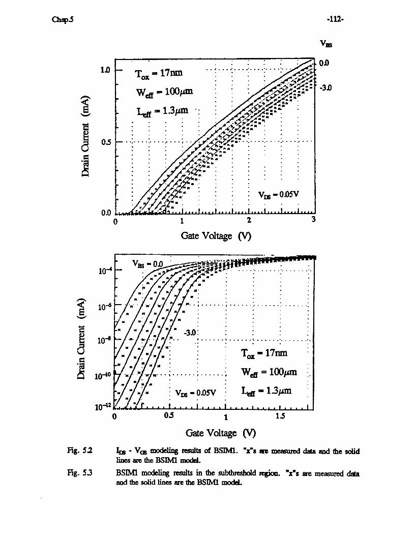
Fig. 5 2
Fig. 53
1D
05
0 .o 0 1 2
Gatevoltage (V)
,
-1l2-
VBS
01)
-31)
I
0 OS 1 1s
Gatevoltage (V)

-11s
1. mobility rechction due to the vertical fidd
2. carder velocity sahuation,
3. draiDinduced banier lmaing.
4. sauce/drain charge shariog.
5. llomuniform channel Qping.
6. channel lcngth modul&on.
7. subthreshold condllcticm.
8. di parasitic resistaace.
9. h o t 4 ~ n - i n d u c e d outplt resistance reduction.
10. inversion-layer capacitance.
E c q t for the last three effects, most of these were alredy included in the BSMl mode€. In
the following sections, these effects were mexamined based on deepsubmicrometer MOS
ms considerations and their implementation in BSIMlL is descn'bed.
53.2 Strong-inversion region
(A) Threshold voltage
It has been shown in ch- 3 that the threshold voltage of propexiy designed deep
submicrometer MOSFEI's does not exhiit severe short-channel effects until the devices are
oear punchthrough. Therefore, the -hold voltage model, E;q.(5.1), used in BSIMl which
already includes most of the important short-chanuel effects such as the d d r a i n charge
sharing, non-uniform channel doping, and draikindud=er-lowering, is retained in
BSIMIL. A typical threshold vd-e for a quarterdcron n-chamel MOS transistor is shown
Rg. 5.4. The asterisks are meanucd data aod the d i d awe is calculated from (5.1). In
BSIMl, the cimh-imchcecCbarrier-lowexing d u e n t q is empi.xically expressed as a linear
function of V, md V,. But in BSlM2, be dependence of q on V,, qB is nmoved since
it does not agree with physical principle and may c81se negative output resistance at low
ament levels if q D has awnmg sign.

1.5
n + U
1.0 !Y c, m
$
2 a m
8 0.5
0
-114-
_ - .
To, - 86 A NMOS Weff = 10 pm La - 0.25 p m Weff = 10 pm La - 0.25 p m
1 . 1 . 1 . 1 . 1 - 1 . ' . ' . ' - '
0.5 0.9 1.3 1.7 2 1
Fig. 5.4 Threshold voltage vems body bias for a qucater micron whamel MOSFET. The ssterisks aremeanuleddataapld the d i d curve is thtmodcl,

-115-
.
Ibe sccumy of a drain a m a t modd is M y diected @ how the vdocity saluratioa
effect is implemented, apedally for deepsubmi- &vices in which the c h d dcctxic
field is high d the drain clll~t quickiy saruratcs. 'Ihe nlltionship bctwetll the caxxicr o d e
Qty eDd the chaanel e l h c fidd har been studied vollious groups [5.19$20]. W of lhc
d t s is shown in Fig. 55 (5391. 'Ihc dots arc mawed dasa md the c w c s rcpreseat
different velocity models which will be described below. 'Ihe most cammonly used dQ.
velocity model is (5.13), becase it leads to simple analytical chin camcat equations.
(r v = l + p J
(5.13)
where & - &-, EV&, p is the mobility, and v- is the carrier satmition velocity. 'Ihe result
of (5.13) is indicated by me1 in Fq. 55. However, this modd undurstimates the h e r
velocity in the low-field region as cao be sea in Fs. 55. A second model, the socalled
"two-section" model [521), was proposed, to improve the tccunxy of (5.13). In the twe
d o n d, a larger Critical field of&-= is used in (5.13) w h E <E, md sets v - v, whea E > E , The result is plotted = awe-2. Although this modcl am achieve betta
~~ccuracy, it results in a discontinuity in the bt duivadive of the drain ament equation d
V-. To retain the high l~ccuracy and yet to rnroid the discontinuity prublan, a compmmised
solution is used in BSM.
when the critid field &starts from alargervalue of&& + Q in the low-field reg;Oa IS
m the twesecticm modd d smoothly CbaDges to & t&V= = V- IS in (5.13). &is a
fitting paramctcr. The rcsult of (5.14) is shown in awe-3 in FSg. 53. The q u a c fuodion
used in (5.14) is to keep the first derivdve of the drain cuzrcllt @on continuals at V ~ T .

-116
IC# t . a
ICW 2 "d I . . . . . . a
. . V = A:
1 + (E/E,) . IC- ' I
IC+2 Ice3 IE- I E+S I C Y Electric Field (Vlcm)
2. E,=2E, ESE,
v =vat E>E,
3.

-117-
(Q Mobility Isduction due to v d d field
It has bcar shown Paaa the d e r mobility cam be explesssd s aunivasal furdon of the
effective vertical electric fidd for a wide renge of oxide t h i c k and c h d doping casea-
tdon (522-5241.
where h, I&, and n are mutants whose values am be fouad in [524], & is the effsctive
vertical electric fidd in the inversion layer given by
(5.16)
4, and $I are the bulk and iqwrsb charge density, respectively. However, Eq.(5.15) is sd-
dom used in circuit analysis for several reasons. Fixst, Eq.(5.15) docs not have a desiie
functional fom for ckcuit simulation purpose becarse of the power function in tbc denomina
tor. Tale 5.1 lists the relative evaludon time required for v&au functions based m 106 4-
culations in a SUN SPARG1 station. 'Ihc evaluadion tkne of a p a function is about 3
times that of an exponential and 120 timer Ehatd asimple arithmetic aperabicm. secoadly,Q,
in the subthreshold w not be errplicitly expnssed s a fuoction of the v01-
tag=, therefore it can mt be dinctly used in most cirarit simulators d d t s in difficulty in
parameter extraction. Thirdly, the parasitic saurcddcain nsistaaoe effect also cases mtllsurcd
mobirity to devi& from (5.15). A more Widely accepted mobility modd is (5.17), which can
be considered as a first-ordtt approximation of (5.15).
For d c e p s u M ~ devices with thin gate oxides, the vertical electric field is too lage
which caws the first-order approaimdm d (5.u) to bacome indexpate as shown in Fig.
5.6, whae the electron d t y for 8.6nm gate oxide &vices is plotted agaiast Vm-V,. 'Ihe
Qss arc meawsd dada and the clashed h e is thebest fit of (5.17). A simple amemrimat to

-5 -1111-
improve the l l xxv~cy is to add higbcr-orda tam to the hamugor * d (5.17). It is f d
that the inclusion of the SdOOtlCCOrdQ term only, (5.18), is am@ for most thin gate axi&
devices undcrIlorm$ bias cooditions ad the result is giveaby the d i d curve in Fig. SA.
'Ihe use of (5.18) also provides BSIM2 with the capabitity to mo&4 the nowmonotun 'c nxM-
ity bthavior with the vettical fidd at low ( 5 2 9
The effect of the SoUrcejdfEdn resistance on device paformance has bctn discussed in
section 33 . In section 33, these parasitic rtsistaoces were frcatcd as external components to
the MoSFETs, but from a circuit shlation point ab view, ddbg extra e l m to each
transistor w d d greatly increase the circuit size and slow &wn tbe simuldon speed.
more, extrecting intrinsic MOSFEI' paoanebs hm wdrinsjc &vice 'csrequire
p i a l care during themeasurerpe~r and Optimizatioaprocsdurs, which w o u l d g d y a@-
cape the param"r txtraction proccss. It am be shown [52q that with a papa sdediua of
the model equations, the parasitic resistrrnce c € f ~ c a n b e l U m p e d i n t o t h e m o b i l i t y ~ In
mobility parameters are extracted fnnn test devices, tbe d d r a i n parasitic nsistaKx efFect
is altomedically included in this rryytl.
BSIM2, the parasitic resistance effect is i n c o p d in (US) rad (5.18). 'Ibcrcfore, w h the
Iu BSIMI, the velocity saturation d mobility rc&ctkm &e to vertical field effects wae
pt togetha through multiplication of (5.15) d (5.17), xcsultjng in a pro&ct tam in tbe
denominator of (52). With such formulation, tk Saturatioo vdodty decreases as tbe grte vol-
*e incrurses which does mt agree With the physid ObsavatiOO thac the Canicr d t m
velocity is ccmstmt at a givea tanpedum, independent d the v d c a l fidd [5.19$20$27].
A more physical approach, which sums the two dkts t o g a , is &ptd io BSM2 rad tbe

-119-
d t i q cfrain cunmt for the linurr region is giva in (5s).

S20.0
440.0
360.0
280.0
208.8 I

chap5 -121-
when E, is given in (5.15). As a mattex of fact, when the channel length is longer thau one
micron, either using a procfuct term or a summa$ 'on term in the deoormnado r of (5.19) hrs vay
little difference, 8s far as the (wwzy~y is concerned. This is shown in Fg. 5.7 where S i m U l d
drain aments for both appmaches are compared to measured data for a device with T, =
8.6nm and = 15pm. 'Ihe dots are measured data and the curves are simulations. The
difference between the two simulation results is negligible. However, as the channel length is
reduced, velocity saturation effects become more important and simulations from the summa
tion approach becomes more 8ccuTafe than the multiplication approach as shown in Fig. 58,
where measured and simulated 1~ - Vm characteristics for a quarter-micron MOSFET are
l'hus far the drain current formulation of BSIM2 in the strong-inversion region is similar
to that of BSIMl listed in (5.2)-(59) except for some minor modifications. Since the homi -
nator in (5.19) is different fmm that in (52), the expression for V, in (58) should be changed
to (520) accordingly.
Fig. 59 shows messured and calculated Im - V, chmckxistics in the hear region for
= 025pm and T, - 8.6nm. The asteaisks are measured data an n-cl~annel MOSFET with
and the solid m e s axe simulation results. 'Ihe dashed w e along V, - OV shows the fesult
if (5.17) is used instegd of (5.18) in the drain current equation, (5.19), ex- the impor-
tance of the second-order term of the mobility mhction effect in (5.18). Fig. 5.10 shows
meaSured and calculated Im - V, charadcristics in the sahuation region for the same device.
Similar figures for a pchannel MOSF" with - OApm and T, = 75nm are shown in Fig.

-5 -l22-
5.11
alsQ
d 5.12.
bcfoundin
More
[5.11]
Tox = 86
W 5 L 1.5
-PI-
can
1
Fig. 5.7 comprhn of modeling results betwan a d o n term md a produd te!am in the denominapor of Eq(5.19) for a "longer" c h d device.

Tox - 86
3
2
3 w
13 M
1
0
W 5 L 0.25 -.I--.--
1
Summation Term
3
2
1
Kg. 5.8
Product Term .%
0 1 2
vm 0 3

-124-
50E-06
0.8 -6 1 e 2 1.8 - 2.4
Gate Voltage (V)

-125-
NMOS
Lea - 0.25 pm t 40E-04
u
Gate Voltage (V)
Fig. 5.10 BSIM2 modeling results in the saturation region for an n-c- device. ?he asterisks are m d data and the solid lines are the modd.

ToX - 75 PMOS
OOE +00 0 .0 L -. 8 -1.6 -2 .4 -3.2 - 4 . 0
Gate Voltage (VI
fig. 5.11 BSIM2 modeliog results in the linear region for a bchmnd &via. 'Ibe astaL ish =measured dataand tk solid lines are the model.

n 4 v
7 -206-04
i -16E-04
ToX = 75 A PMOS Wa-5pm Lea - 0.4 pm
00E+00
-1.6 - 2 . 4 -3.2 - 4 0.0 -. e Gate Voltage (VI
.0
Fig. 5.12 BSIMIZ modeling results in the satudion region for a pchannd device. 'Ih+ asterisks are measured data and the solid lines are the model.

chap5 -128
53.2 Subthreshold region
’Ihe drain current in the subthresholdrrgion is *by t h c d i f F u s i o n ~ [527].
Using the chargashed approXimation [528], the subthreshdd currerd of a MosFEf cm be
exHesd=
A quick derivation of (521) is given in Appendix C However, Eq.(521) wn not be directly
used unless & can be expressed as an explicit function of the terminal voltages. A relationship
between the gate voltage, Vm, and & has been dexived in [5.27], but it is too ooolplicaded to
be used in circuit analysis. In BsIM2, a simple appmximation is used which will be desc r i i
below. Fig. 5.13 shows a plot of & vemus Va - Vm calculated froin lwo-&mensionrd
analysis. It is found thalk in the subthreshold region c811 be axumtdy approximated as a
hear function of V, with slope nV, and y-intercept -V, as drmn by the dashed in in fig.
5.13.
where n is the subthreshold swing coefficient givm by
GI n=l+C,
and
A detailed derivation of
(525)
(523)-(525) cm ills0 be found in Appendix c substituting (523)

-129-
into (521), the subthreshold curzeaf can be mvntten IS
Eq. (526) can further be simplified to yield
where all the missing tenns in (526) are incorporated into the fitting panmetex V,, which
accounts for the threshold voltage offset between strong-inversion and subthreshold regions.
e. e I . I ) 2 .I) 3.8 1.) f. I
'GS -vFB
Fig. 5.13 Surfixe potential versus gate voltage. ?he dashed line is a hear approximation of the d a c e potential in the subthreshold region.

chap5 -130-
533 Transition regiao
(A) Inversion-layer mtmcc d k t
When the gate oxide thiclrness becomes comparable to the depletion-layer thickness 8s in
in most deepsubmicrometer devices, the inversimlayer czptxiw effect is no longer negligi-
ble and has to be included in MOSF" modeling especially for low gate vdtage operdoos.
Fig. 5.14 shows calculated inversion charge density as a fuection of the gate voltage for a T,
= 8nm device. ?he stmight line in the same figure repnsents the usual linear approximation
given by &(V,-V&. Because of the inversimlgra capacitaoce &ea, the inversiall
charge density deviates from its linear approximation when the gate voltage is near the tbs-
hold voltage. ?his deviation increases as the gate oxide thickness decreases. Although the
drab current equations in both the mng-inversion and the subthreshold regions can be
derived, there is no simple analytical expression for the drain currenf near the threshold vol-
%e-
In this m&, a transition region between the strong-inversion and the subthreshold
regions is determined. ?his transition region is marked in Fig. 5.15. A cubic spline function
of V, is created for this region to axamt for the inversion-layer capacitance effect. Ihe
upper and lower bound of the transition regiOn can be dculated from the equivalent Circuit
shown in Hg. 5.16. The effective gate cap9citance Ch of a MOSFET looking into the gate
terminal is equal to C, in series w i t h a .
where C, is defined 8s W d k
( 5 W
and can be expressed as (529) in the subthreshold region
Using the same approach used in the chivdon of (527), & cau be approldmatad as

-131-
50.8
0.0 A .0 1.2 1.6 2.8
Rg. 5.14 Channel inversion charge density versus gate voltage calculated iium twe dimensional analysis. 'Ihe straight h e is the usual qproximation given by cdV,-V,)*

-132-
lo4 - 10-7' -
n 4 - m CI w
10- 0 0.4 0.8 1.2 1.6 2.0
Hg. 5.15 I>rain ament V~ISUS gate voltage in logarithmic scalei illustr&g the smooth tmsition from subthreshold region to the strong inV&on region.
Fig. 5.16 Equivalent capacitance circuit of a M O S m looking into the gate.

-5 -13%
~n the stmng-immsion region, c is lul~h larger tfian G, w o r e , C&G. TES is
where the linear appmxim&ion Q,<(V=-Vth) is valid. In the subthreshold region how-
ever, C, is much larger than &. 'Ibis is where the cliffusion current dominates * Bycornpar-
bg the relative magnihrdes of C, and & dong V=,the thelowerboundVa andupper
bound V, of the transition region can be determined. For example, if we define the Iowa
bound to be at which C,-lOOG, then Va wiU be
Similarly, the upper bound, defined at &, = lOOC,, can also be calculated.
The width of this transition region ( - Vm - V a ) is about 02 - 03V depending on the oxide
thiCkLMXS.
An effective gate voltage is created in this region by using a cubic spline function of
where the coefficieats cs are to be detearmned from the boundary conditions. 'Ihe drain
cunent equation used in the eansition region is the same as that in strong-inversion region
except V& is used instead of v,. his cubic *e function also serves as a means to
acQuire a smooth transition from the subthreshold region to the strong-inversion region. Ihe
reason to use V& for tht cubic spline function in this region rather than using the drain
CulIMt directly is to simplify the boundary conditions. l l i s approach avoids the need to deter-
mine whether the linear region or the -00 region drain curzent equrSions should be used
at the upper bound

chap5 -134
At the lower bound, Vm - Va, the bamdary conditions am
and at the upper bound, Va - Va, the boundary conctitions
v;, =vc;z
Substituting (534) and (535) into (533), the coefficients of the cubic spline function,cs can
be determined. ?he solutions for these coefficients arc given in Appendix D.
(c) Modeling results
The measured and calculated subthreshold char~~terktics of an D and p-channel devices
are shown in Fig. 5.17 and Fig. 5.18. In Fig. 5.17, three regi0as madred A, B, and C for the
V, = OV a w e indicate the subthreshold, transition, and sfroag-hversiOn regions when the
three different drain ament equations wen uscd. A smooth transition between the regions is
observed.

-135-
h
W
Y
4
Fig. 5.17 B S M modeliDg results in the subthreshold region for an nchannd device. 'Ihc askrisks are m d data d the d i d lines are the 4.

- 1 E-a4
- 1 E-05
- - - - V,--O.OSV :
1 . 1 . 1 . 1 . 1 , 1 , ~ , 1
-0.8 -1 .6 -2.4 -3.2 -4.0 Gate Voltage (VI
I d 6 -1
E-09 i -1E-13
0
fig. 5-18 B S M modeling I t s in the subthreshold region for a pchamd device. The m s k s are rneasmd data and the d i d lines are the modd.

-137-
53.4 Output resistance modding
Although the outpt resistance & is m e of the most importmt perameters in analog c i ~
cuit designs, few MOSFET models can simulate & accwdy. meal autput resistance
charactenstic of a short-channel MOSFBI' is shown in Flg. 5.19. 'Ihe shape of the artplt
resistance in the saturation region can be attdmted to three mechanisms: drain-induced barrier
lowering, channel 1- mocblation, and bot-electron induced cutplt resistance reduction. In
most MOSFET models, the drain-induced-eer lowering &ect is included in the threshold
voltage. In BSlM2 this ef€ect is modeled by the q pammder, therefore in this section, only the
other two effects will be discussed.
(A) Channel length modulation
When the drain voltage is larger than VmAT, the velocity saturation region extends
toward the source, which effectively &ces the channel length and results in a non-zero chan-
nel conductance (or finite R,,J in the saturation region [5.29,530]. A schematic diagram of
the channel length modulation is shown in F4g. 520.
Channel length modulation is the dominant mechanism affecting & when V, is near
V,, This effect is usually implemented in the model through the Bo parameter. BecaPrse of
the reduced channel length, the chaunel conductance coefficient, BO, increases as V, increases.
where & is the chanael length reduction due to the channel length modulation &e&
According to a quasi-2D analysis [531332], LyaM is zero when the drain voltage is less
than VmT ahd increases logarithmically with V, adter Vmp A qualitative r d t of the
quasi-2D analysis is plotted by the solid a w e in Fig. 521. In practice, however, it is found
empirically that the combinatian of a h+c taugent function and a quadratic functjon is
more ac<wate and approPriate to model & when V, is near V ~ T .

-5 -l38-
when Bo and B 8 8 c the amdu- d d e n t s extraded at linear md -on regions,
=q=tivelY, B2, I%, 4 B4 fittiog paraneta, ad Br - 8,-(BO+4Vm-P,Vib. A*-
M v e sketch (537) is plotted by the dashed curve in Fq. 521. In (537), the cnhdmce
coeffideat @ starts to increase from V, - 0 which is Merent from the @2D dys is .
Eq. (537) also eliminates the aiscontinuity problem at Vmp "he ef€& of each in
(537) on the shape of & is indicated in Fig. 522 which atso rev& the mems in which
these parameters can be extracted from meanued data
. As the drain voltage increases beyond VmAT, the peak e l d c field in the velocity
saturation region increases sharply and electron-hde pairs are generated due to impact i&
tim [533,534]. 'Ihe holes generated are collected by the substrate is referred to as the sub
strate wrent Ism. When the substrate ament flows through the substrate, it slightly forward
biases the source junction with respect to the substrate becau~e of the ohmic voltage drop VI,
( - I s d m ). ?his positive body bias (for NMO6) reduces the thrtshdd voltage camsing the
drain current to increase and in turn ckgndes the outplt resistance [53]. This process is dep
icted in Fig. 523. Therefore, to the first-0rde.r apprordmatioa, the d t a n t drain d o n
current I k T due to the hot-electron effects caa be expressed as
where I ~ T is the Qain saturation current without hot-electron effect &ea by (5.6), &UB is
the effective resistance of the substrate, and C is a constant. Substituting the substrade cumat
equation, (324), into (538), Eq. (538) can be rewritten ES
where A, and are impact ionization wcffidents. Under n o d bias ConditiOnS, the second
term in the brackets is much smaller thm OM, henct (539) has very little e f k t on the magni-
tude of the calculated drain current, but it has Significant effect on the output resistance as will

be shown later.
-139-
-- .
Triode Region Saturation Region 10E +e+ I . I - I
80E+03 - - ,
68E+03 - e v - cr a #" 40E+03 -
i 20E+03
d I
& I I
* I 1. . 00E+00 ***
0.0 06
Effect
Fig. 5.19 weal a u p t resistance characteristics of a shortchannel MOSFET.

-140-
I I I
Fig. 520 A schematic diagram showing the chamd le@ tm&lation &at.
VDSAT
Posat
Fig. 521 Qualitative plots of thc conductance coefficient versus drain vdtage. The solid tame is the d t of a quasi 2-D analysis and the dashed curve is the B S M 2 model.

-141-
Fig. 5 2 2
Drain Voltage
resamce vetsus drain voltage showing the effects of various BSM2 parameters on the shape of the outpt re&tance.

-142-
I J
Rg. 5 2 3 A schematic diagram showing the process of outpt xtxktance rexbction due to hot-elcdron d€ccts.

-143
Fig. 524a b s measured d calculadbd I= - V= characteristics of a quarter-micrOn
n-channel MOSFEI: The comqxmchg autpt resistaxe is shown in Fig. 524b. 'Ihe ~wz f -
rate Ins and & modeling results make BSIMIZ highly suitable for both digital and andog
applications.
As illustrated in the design a w e s developed in chapter 4, hotelectron reliability has
becume the major concern in deepsubrnicnweter device.and circuit design. To predict the
device Iifetime andor aged circuit behavior due to hotelectron &ects have also become one
of the design steps in VLSIKJLSI systems. Recently, various activities in this area have bees
reported [535-5381. More programs are expected to be developed in the future. In these pro-
grams, model parameters from both fresh and hot-electron stressed transistors are usually
required. Therefore, a MOSFET model for the future s h d d serve well for this pupose. To
test BSIM2's capability in modeliog stressed devices, the device used in Fig. 524 was pr-
posdy degraded by hotelectron stress to generate a threshold voltage shift of 022 volts, then
model parameters were r- from this device. "he modeling results are shown in Fig.
525. Again, very good agreement between measured and calculated Im and & are observed
which proves that BSIM;! is also a potential candidate for Circuit aging related simulations.
Since the LDD structure has become common in ament technologies, a MOSEET model
will not be useful if it fails to model LDD devices. BSJM2's capability in this aspect is
verified in Fig. 526 where measured and calculated I= and for an LDD transistor are
shown. Finally, the modeling d t s for a non-LDD pchaanel transistor are shown in Fig.
527.

-144-
2.K-83 I T,, = 8.6nm NMOS - L - - -
--- Drain Voltage (V)
(a) BSIM2 I= - V, mo&ling results for a quarter-micron n-channel device, The asterisks arc meErmnd data and
the solid lines are the modd.
Fig. 524 0) the CorresPoMhng cwJut -

-145-
2.61V
183V
Drain Voltage (V)
Fig. 5 2 s (a) BSIM2 I= - V= modeling results for a quarter-micron n-channel device after hot-e!ledr~n stnss. 'Ihe threshold voltage shift is 022V. (b) thc coxresponding outpt resistance. 'Ihe &sks are meamred data and the sdid linesZU!5thCmodd.

I .st* T,, = 125nm NMOS
4.06V n 4
cB.Ic41 - tl
.- cc.eE-83.
Y
w
L 6 3.12v
ii a
2.17V
2.a 3.8 4.a 8.0 1 .8 Drain Voltage (v)
Fig. 526 (a) BSlM2 - V, modeling results for tm OGhannd LDD device, (b) the corresponding cutpt resi-. The d s k s are measured daka and the d i d linesaretfitrmdd,

-147-
e v t t
Fig. 527 (a) BsTM2 - Vm modeling d t s for a p - c h d &vice, (b) the corresponding outprt resistance. 'Ihe d s k s am measured data and the d i d

-148-
5 3 5 Bias-dependent parametaJ
So far, 18 SI342 parmetes havekm descxihd. SaneoftheseparaDetas rae f a d
to be slightly biasdependent which are approximated by liocar €imcticms of biases. AU of
these -, dong with the equations danonstratiq their b i a s d e p e m a e ~ are listed
below.
1 7 . 4 = & + Ag
18. Bj Ba + Bg
Note that the biasdependencies of prametas 5 and 15 arc H e r e n t from those in BSIM1.
They are more physical now. & and &) in (5.14) have been @aced by VI and Urn,

-149-
respectively ES in BSIMl, wherc &=-.
53.6 Size-independent parameters
'Ihe parameters extmted from a test device only pertain to that particular device size.
'Ihe parameter set for each device size is r e f e n e d to a "parameter file". Several Siza
dependent "parameter files" can be procased to generate a set of S idependent parameta
called a "process file". The equation used in BSIMl to generate the "process file" is given in
(5 .a).
PL pw p(4, WJ =Po +- +- 4 Wi
where P&, WJ is a parameter for a padcular effective length 4 and width Wi, Po, PL and Pw
are the sizeindependent parameters. A schematic dirlgram of this proudme is shown in Fig.
528. The Size-independent pparanetrrs arc generated by fitting parameter files with different
device dimensions (Lt's and W<s) to (5.40). Once PO, PL and Pw ace known, the model
parameten for a device with any channel length and width can be calculated from (5.40) by
replacing 4 and Wi with the desired dimensions. Detailed description of this procedure um be
found in [5.11].
Although (5.40) does not wo& wdl wheo the rmge of the device dimensions is wide, for
exampIe~>lO,itissti l lkeptinBSIM2forthetimebeing. Ifawiderangeofdevice
dimensions has to be used in a circuit design, breaking the process fde into two or more pro-
cess files with d e r device dimension m g e s is recommended. Studies on improving (5.40)
areundexway.

-150-
a
Process file
Para. Para. filen ~ m m m m m ~ m m m
Para. file1 file2 Ll9 Wl L29 w2 Ln, Wn
m m m m m m m m m m
t
PW PL P=P*+- Leff weff
+-
5.4 Parameter extraction for BSIM2
-151-
An IBM FGbascd integrated system has been develqzd for autom&cd d o n of
BSM2 parametas. In this section, only a g m d ov&ew of the system is dcscn"bcd. A
cunplete description ofthepram&erextraction systan,useiS guide$ andcxqies aregival
m [S.ll].
5.4.1 Automated parameter extraction system
A schematic diagram of the system hardware in shown in Rg. 5.29. "his system Consists
of three major parts: an IBM PS/z (model 50 or higher) or a €CAT complter with a VGA
graphics card running under Dos 3.0 or higher @os 4.0 or higher to enable VGA screen
dump), an HP4145 paramebic analyzery and a manual probe station. An IOtech GP48812 inter-
face board is required in the computer to Commuoicrde with the HP4145 parametric analyzer.
The extraction program is written in Microsoft C veasion 5.1 with d e d IOtech Per-
sonal488/2 modules. 'Ihe executable code is about 310KB.
@) systan operation
Fig. 5 3 0 shows the flowchart of the parameter extraction progtmn. The program is
modular and menu-driven for easy operation and future modification. 'Ihe only required user-
supplied inputs are the device dimensions, dit location, supply voltages, and the SMU
(Stimulus-Meawement Unit) Connections for the HP4145 pammekz andyzer. 'Ihe functions
of the parameter extraction system are grouped into two categories: single device mode and
multiple device mode. In the single device mode, parameter files are extraded from each dev-
ice. In the multiple device mode, a process file is created hnn user selected parameter files. In
either mode, calculated I-V charaderistics cau be displayed togethex with measured d t s for
comparison. Dwice I-V data caa be either meawed directly from physical devices thruugh
the Hp4145 paramhc analyzer or read back from a hadfloppy disk. If the I-V data are to

-5 -152-
and the last two data sets are used to extract cupt-resistmcc related pamnetm, (537>(539).
The playback featwe of the program then allows the usen to check the quality of the extractbd
parameters for each device. 'Ihis extraction process is repeaded every time the single device
model operation is executed. ?he total extraction time for each device is about 20 - 30 seconds without measurement and about 2 minutes with measurement on a PS/2 Model 50
computer. After a few devices have been extracted, a prows file may be created.
5.43 Extraction algorithms
?he most commonly used technique in parameter emtion is the nonlinear global aptin-
ization [539-5.421. Although global Optimization wil l give the minimum avenge emr
between calculated and measured results, the extracted parameter values may not be physidy
meaningful which makes interpolation or extrapolation of parameters for other device
sions very difficult and unreliable. Also, the optimization processes are usually slow, since the
compltation time incresses drastically with the number of pametem. Most of all, if some
parameters are mutually correlated in the model, the o p h h t i o n plocess becomes difficult to
m e r g e or may d t in non-uniye solutions. Various auxiliaoy me&~ods such LIP
Levenberg-Marquardt method [5.43,5.44], modified Gam method [5.45,5.461, and the steepest
descent mehod I5.471, etc., are incorporaded into the global ophhation process to expedite
the convergence or to midmize the effect of parametex redun-. 'Therefore, parameter
extraction programs adopting the globat optimization technique are always quite corzlplicatcd.

manual probe it station
I E E E W B U S r] HP4145 -
I I
I- I SMU1-4
r printer
Hardware Platform
IOtech GP488/2 interface board
HP4145B parametric analyzer
VGA graphics capability
Parallel Printer
IBM model 50 (or higher)

1 I - U n t v l z t p u a m e k n 1
Safyfatlon Rea lon Parameter Ext ractiQn
8 lkxtrad subthreshold Parametem
Putbut Resista nce Para mter Ext racw
Fig. 530 Flowchart of the BSIM2 cxtnxtim Prognm.

-5 -155-
Ihe to the mathematically compgcf functiooal forms d the BSIM2 modd, a l d Optimi-
zation technique together with a physi- paranetrr extrtajon method am be anplaysd
to extract BsIM2 parameters. Becalse no sophisticated algorithms m needed with this
appaoach, the pameter extraction progran can be easily implement and the pmmctas
extracted are also more physical and reliable than those fn>m global 0pthhtior.w. With local
opt;m;zatian, d y two or three param&s ate cxtracted at atime under a certain bias condition
and the optimization process is qeated to cover all upemtion regions until all of the parama
texs are extracted. Since only two or three parameters rn optimized each time, the o p t i n k
tion p m s is very fast. ?he nonconvergence and non-uniqueness problems usually do not
exist.
In the BSIM.2 parameter extraction program, the only 0pt;m;Zation process is a combina
tion of Newton-Raphson's iteration and a linear least-square fit routine with two or three vari-
able.~. "he flowchart of the opt;m;zaSion process is shown in Fig. 531. The model equations
are first arranged in a form suitable for Newton-F&phson's iteration as shown in (5.41).
(5.41)
where fo is the function to be optdzed, Pl, P2, and P3 are the parameters to be extradcd, PlW
Pb, and Pk stand for the true parameters that we are looking for, Plm), Pim), and P$")
represent the parameter values after the m* itemtion. III mi case, the function fo may be the
drain current equation or its variational form, and f(Plo,PbP& would be measured I-V dada
To make (5.41) ready for the linear least-square fit routine (a form of y =a+bxl +cxz), both
sides of (5.41) arc first divided by 8f/8Pl. Thea the measured I-V data are fitted to (5A1) and
the increments of parameteas for next iteration, L P ~ ~ ~ S , are determined, be prameta value^
for the (mg)* iteratia are given by
pi"' =pi'"' +&p) i=1,2,3 (5.42)
' Ihis procedure is qeated until all b p i ' s are smaller than some p n x b m ~ ~ ~ * ed values, at this
point the opt inh ion process is considered converged.

chap5 -156.
ple shawing how tbe optimjzeaioa pmccss is pllyskdy applied. Exst of d, the drain culzmt
equation in the linear e o n (5.19) is matmged in such a fann suitable for (5.41).
where G = I&Vm is the measured chanacl condudmce.Tbe QV, termin rhc demunm& * r
of (5.19) hm been dropped in (5.43), since Vm is & (0.1V) compared to Vm. S~bstit~tiag
(5.43) into (5.41), the equation used in the Newton-Raphson’s iteration can be obtained
where
and
-= a 2
v,-v*--v,
(5.45)
During each iteration, the same measured 1, - Va dppa are fitted through (5.44) to ddate
&?Am), &Jim), and for mxt ite,ratioa. ’Ihe itemtion is tPrmjnaied when the increu~eats of
all three patameters arc less than 0.01% of their ammt values or when a preset maximum
iteration numbef is reached.
For each substrate voltage, a set of Bo, Vu ad I& arc extracted. ’Ihese pammeter vducs
may exhibit slight substrate birr, ckpdemc and are fitted through ahear equation as listedh
section 535 to extract the subsmte-bias dependent parcanetess.

-157-
Initial estimates of parametas P,,
<
Fig. 531
Model quatiorw
calculated values
Measured data 3
* fi
v
Linear least S q w
fit routine 1 d

5 5 SPICE simulation results
-158-
The BSlM2 model has been in.@& SPIcE3.Cl. A program list of the
BSIMevaluate.~ module, which evaluates the BSM model expaions in SPI-, is giva in
Appendix E An cxBmple of SPXCEiaplt deck with BSlM2 model m r s is shown in
Fig. 532. BSIM2 model has been used to simulate an NMO6 cahmementdpletion type
ring oscillator with T, = 8.6m and - OBpn The simulaled delay time is 24ps/stage,
very close to the measured data of 22ps/stzige.
The 8c~ll8cy of the BSIM2 model has been demonstrated in section 53. More results
can be found in [5.11]. In this section, the computational efficiency of the model is discussed.
Table 5 2 shows the comparison of SPICE simulation times required for BSIM2,level-l, and
level-2 models on two typical circuits. The device dimensions used in the simulation were T,
= 25nm and & - 2pm for level-1 and level-2 models; T, = 8.6m and & - 025,05, and
0.7pm for BsIM2. The parameten for level-1 and level-2 models are typical values for 2-p
technology provided by MOSIS.
'Ihe first simulalion is a DC aaalysis of five I= - V, charaderistics. Althaugh the
evaluation time of BsIM2 model itself is slower than that of level-1 model and comparable to
that of level-2 model, the total cotuptation times required for BSlM2 in this simulation is
similar to that of level-1 mode4 a d twice as fast 8s that of level-2 model. This is bezause the
number of iterations needed in the simulation for BSIM2 is less than those of the other two
models due to BSIM2's smoother functional form. Ihe total number of iterations for each
mc&l are also shown in Table 52. The second simulation is the traasient analysis of a 15-
stage CMOS ring oscillator. Similar results wen also observed. More simulations on analog
circuits aTe mdemay.

chap5 -159-
AN 11-STAGE CMOS RING OSCILLATOR WITH TOX-86A AND LEFF-0.3UM .SUBCKT INV 1 2 3 c1 3 0 0.1P M1 3 2 1 1 PMEN L-0.3U W=30U AD-lZOP AS=75P PD-36U PS-6U M2 3 2 0 0 NMEN L-0.3U W-15U AD=60P AS-37.5P PD-23U PSm6U .ENDS INV x1 21 2 3 INV x2 1 3 4 INV x3 1 4 5 INV X4 1 5 6 INV X5 1 6 7 INV X6 1 7 8 INV X7 1 8 9 INV X8 1 9 10 INV x9 1 10 11 INV x10 1 11 12 INV X11 1 12 2 INV VDDl 1 0 4.0 VDD 2 1 0 PULSE(0 4 . 0 0 0.5N 1N 500N) .TRAN 60P 60N .PLOT TRAN V ( 2 ) .PRINT TRAN V(2) .OPTIONS VNTOL-1E-5 ABSTOL-1E-9 ITL4-50 + CPTIME-lE4 RELTOL-0.01 CHGTOL-1E-12 PIVTOL-1E-29 ITL1-500 ITL2-500 .OPT ACCT .WIDTH OUT-80 .model NMEN nmos level - 4 + vfb -1.0 lvfb 0.0 Wfb 0.0 + phi = 0.889 lphi - 0.0 wphi - 0.0 + kl = 0.93 lkl = 0.0 wkl 0.0 + k2 - 0.125 lk2 = 0.0 wk2 = 0.0 + eta0 - 0.017 letaO - 0.0 w e t a O = 0.0 + etab = -0.007 letab = 0.0 wetab - 0.0 + mu0 = 327.3 dl = 0.0 dw - 0.0 + muOb = -8.42 lmuOb = 0.0 wmuOb = 0.0 + musO = 431.8 lmus0 - 0.0 mus0 = 0.0 + musb = -7.4 lmusb - 0.0 wmusb - 0.0 + mu30 = 15.1 lmu30 - 0.0 mu30 = 0.0 + mu3b = -1.34 lmu3b - 0.0 wmu3b = 0.0 + mu3g - -2 lmu3g - 0.0 wmu3g - 0.0 + mu20 = 2.37 lmu20 - 0.0 wmu20 9 0.0 + mu2b = 0.09 lmu2b - 0.0 wmu2b = 0.0 + uaO = .443 luaO - 0.0 ma0 = 0.0 + uab - -0.025 luab - 0.0 wuab - 0.0 + ubO - 0 . 0 7 5 l u b 0 - 0.0 wubo 0.0 + ubb = -0.0076 lubb 0.0 Wbb 0.0 + u10 9 0.18 lul0 0 . 0 wul0 = 0.0 + ulb = 0.00014 lulb = 0.0 wulb = 0.0 + nO = 1.125 In0 = 0.0 wnO - 0.0 + nb - 0.35 lnb - 0.0 w n b = 0.0 + nd - -0.017 lnd - 0.0 wnd - 0.0 + vofO = 1.16 lvof0 = 0.0 wofO 0.0 + vofb = -0.034 1~0fb 0.0 Wofb 0.0 + vofd -0.069 lvofd 0.0 Wofd 0.0 + ai0 - 332.68 laiO - 0.0 waiO - 0.0 + aib = 108.55 laib - 0.0 waib - 0.0

+ biO = 24 .62 lbiO = 0.0 ubi0 = 0.0 + bib = 2 .92 lbib = 0.0 w b i b - 0.0 + v g h i y h = 0.232 lvghigh = 0.0 wvghigh = 0.0 + vglow = -0.114 lvglow 0.0 wvglow = 0.0 + tox - 8.6e-3 t emp = 27 vdd - 3 vgg = 4 vbb = -3 + cgdo = 2.0e-10 cgso - 2.0e-10 cgbo - 5.0e-11 + x p a r t = 0 + r s h = 10 c j = 0.0002 cjsw = 1.0e-10 + js = 5e-5 pb = 0 . 7 pbsw = 0.8 + m j - 0 .5 m j s w - 0 . 3 3 w d f = 0 + del l - 0 .model PMEN pmos l e v e l - 4 + vfb -1.0 lv fb 0 .0 wvfb = 0.0 + p h i - 0 .889 l p h i = 0.0 w p h i - 0 .0 + k l = 0 . 9 3 l k l = 0.0 wkl - 0.0 + k2 = 0 . 1 2 5 l k 2 - 0 .0 wk2 - 0.0 + e t a 0 = 0.017 letaO = 0.0 wetaO = 0.0 + etab = -0 ,007 le tab = 0.0 w e t a b - 0.0 + mu0 - 131 d l = 0.0 d w = 0.0 + muOb = -3 .42 lmuOb = 0 . 0 wmuOb = 0 . 0 + musO = 1 7 3 . 8 lmusO = 0 . 0 wmus0 = 0 . 0 + musb = -3 lmusb = 0 . 0 wmusb = 0 .0 + mu30 = 6 . lmu30 - 0 . 0 wmu30 = 0.0 + mu3b = -0 .6 lmu3b = 0 .0 wmu3b = 0.0 + mu3g = -0.8 lmu3g = 0.0 wmu3g = 0 . 0 + mu20 = 2 . 3 7 lmu20 - 0 . 0 wmu20 = 0.0 + mu2b = 0 .09 lmu2b = 0 .0 wmu2b = 0.0 + uaO = . 4 4 3 luaO = 0 .0 wuaO = 0.0 + u a b = -0 .025 l u a b = 0 .0 wuab - 0.0 + ubO = 0 . 0 7 5 lubO = 0 .0 wubO = 0 .0 + u b b = -0 .0076 lubb = 0 .0 wubb 0.0 + u10 = 0 . 1 3 l u l 0 = 0 .0 wul0 = 0.0 + u l b = 0,0001 l u l b = 0.0 wulb = 0.0 + nO = 1 . 1 2 5 I n 0 = 0.0 wnO = 0 .0 + n b = 0 . 3 5 l n b = 0 .0 w n b = 0.0 + n d = -0 ,017 l n d = 0.0 wnd = 0.0 + vofO = 1 . 1 6 l v o f O = 0 .0 wvofO = 0.0 + vofb = -0.034 lvofb 0 .0 wvofb = 0.0 + v o f d = -0.069 lvofd 0 .0 wvofd 0.0 + ai0 = 0 laiO = 0 .0 w a i O = 0.0 + a i b = 0 l a i b = 0 .0 waib = 0.0 + biO - 0 lbiO = 0 .0 w b i O = 0.0 + bib = 0 l b i b - 0 .0 wbib - 0.0 + vghigh = 0.232 lvghigh = 0.0 Wghigh = 0.0 + vglow -0.114 lvglow 0.0 wvglow 0.0 + t o x = 8 .6e -3 t e m p - 27 vdd = 3 vgg = 4 vbb - -3 + cgdo = 2.0e-10 cgso = 2.0e-10 cgbo - 5.0e-11 + x p a r t - 0 + r s h = 0 c j = 0.0002 c j s w = 1.0e-10 + js = 5e-5 pb = 0 . 7 pbsw = 0.8 + m j - 0 . 5 m j s w = 0 . 3 3 wdf - 0 + d e l l = 0 . END
Fig. 532 An exEpLlplc of SPiCE3 inpt deck for an 11-me CMO6 % oscillator with RsMparametes3.

-161-
SPICE Simulation Results Measured delay time: 22psktage Simulated delay time: 24psktage (NMOS E-D ring. osc., Tox=8.6nm, Leff=0.25um)
Model I
Circuit
Time (s) Iterations 1 Circuit -1 Time (s) 1 Iterations1
Level 1 250 2.0 DC Ar 1.51 113
TRAN 185.4 576
Level 2BSIM2 I BSlM2 I BSIM2 I I I
250 I 86 I 86 I 86 2.0 0.25 0.5 0.7
alysis, Id-Vd characteristics 2.80 I 1.55 I 1.49 I 1.52 111 I 71 I 71 I 71
I I I
Analysis, l5stage ring osc. ----- 173.7 142.7 152.6
1 - ---- 435 342 369
Table 5 2 Comparison of SPICE simulation times between the BSIM2 model and level-1, level-2 models.

-162-
5.6 References
G. Baccarani, M.R. Worchm, and FW. Dennard, "Gencrdkd scaling 'Ihcory and
Its Application to a 114 Micromdu MOSFET Design," IEEE Tran. on Electn>n Dev-
ices, vol. ED31, no. 4, pp.452-462, April 1984.
P X KO, "MOS L)evice Modeling for C h 6 t Sidation," IElDM Tech. Digs., p 488,
1985.
E Hsu, P. K. KO, S. Tam, C. Fb, and R S. Muller, "An Analytical Breakdown Model
for Short-Channel MOSFETs," IEEE Tran. on Electron Devices, vol. ED29, p.1735,
Nov., 1982.
M.-C. Jeng, PX. KO, and C. HI, "A DeepSubmicrometer MOSFET Model for
Analog/Digital Circuit SimulationS," IEDM Tech. Digs., pp.114-117,1988.
PX. Chatterjee, W X Huntex, T.C HEdloway, and Y.T. Iin, "The impact of scaling
laws on the choice of nchannel or p-channd for MO6 W I , " I E E Elm Device
Lett., vol. EDGl, no. 10, p. 220,1980.
H. Shichijo, "A re-examination of p d c a l pedoxmance limits of scaled n - c h d and
pchannel MOS devices for MSI," sdi&State Electron, vol. 26, no. 10, p. 969,1983.
K.K. Ng and W.T. Lynch, "The impact of intrinsic s e i s resistance on Mmm seal-
ing," IEEE Tran. on Electron Mct, vd. ED-34, no. 3, p. 503,1987.
T.L. Quarles, "Analysis of Performance and Concergence Issues for Circvit Simula
tion," Univ. of califomia, Berkeley, Meanoranh no. UCBERL, pu189/42,1989.
TL Quarim, "The SHCE3 ~ e m e o t a t i o n Guide," Univ. of califomia, Berkeley,
Memorandum no. ucB/ERL M89/44,l989.
T L Quaries, "SPICE3 Version 3Cl Users Guide," Univ. of California, BeIlceley,
Memorandum no. UCBERL, M89/46,1989.

chap5 -163-
[SUI J. I>uster, "Parmetex Exhzctioa for BSM," Master 'Ihesis, universi~ of Womia,
Bedreley, 1990.
[ 5 Z ] SJ. Wmg, J.Y. Lee, and C.Y. chaolg, "An Efficient and Rdiable Approach for &m
iconductor Device Parawer &trdon," IEEE Tran. on COmplter-Aided Design, vd.
CADS, no. 1, pp. 170479, Jm. 1986.
[S.l3] CJ'. b h a l a , P.C. P-, d P. Yang, "An BKcient Algorithm for the Ekhactioa
of Pmmeters with Hgb confidence from Nonlineap Modds," Electron Device Lettas,
vol. EDL7, no. 4, pp214-218,1986.
[5.14] B J. Sha , D.L. Shsufetter, P K KO, a d M-C. Jag, "BSIM: Berkeley ShOrt-Channel
IGFEI' MODEL for MOS Transistors," IFEE J. of Solid-State Circuits, vol. SG22, no.
4, Aug. 1987.
[5.15] AH.-C. F i q , "A Subthreshold Conduction Model for BSIM," Univ. of California,
Berkeley, l3C memo. no. UCBh3L, h48542,1985.
[5.l6] BJ. Sheu, DL Scharfetter, and KC Poon, "COIIIpact Short-Chand IGF" Model," Univ. of Califomia, Berkeley, ERL, memo. no. UCB/ERL M84/20,1984.
[5.17] C.S. Chao and LA. Akers, "DrabVoltage EBl- on the lhreshold Voltage of a
Small-Gxme&y MOSFET," Wd-State Elechmics, vd. 26, no. 9, pp.851-860,1983.
(5.181 M.-C Jag, BJ. Sheu, and PX. KO, "BSIM Parameter mti~n - Algoithm and
Users Guide," univ. of California, Memo. no. UCBhBL W/79,1985.
[5.19] RW. Coen and RS. Muller, "velocity of Stdace carders h Inversion Layers on Silk
con," Solibstate Electmics, vd. 23, ~35,1980.
[ S a ] J.-P. Le&ton and G E Dorda, "v-E Dependence in Small-Sized MOS Transistors,"
DFEE Tran. on Electron Devices, vol. ED29, no. 8, Aug. 1982.
(521) C.G. Sidini, P X KO, and J. M d , "The Wed of S g h Helds on MOS Device aad
Circuit Perfonnance," Tran. on Electron Bvices, vd. D31, no. 10, pp. 138&
1393, oct. 1984.

S.C. Sun and J.D. Plummer, "Electron Mobility in hersion aod A#.urmlation Layers
OCI T h d y Oxidzed Silicon Surf-, " IEEE Tm. on Eecbw Devices, vd. Ep
27, p.1497, August, 1980.
AG. Sabnis and J.T. Clem&, "cbaractenzah * 'on of tfie Hec&on Mobility in the
Inverted dOO> Si Surfax," IEDM Tech. Dig., pp.l8-21,1979
M-S. L i q , J.Y. chai, P X KO, and C. €b, "Imrersi~~~-%a C a n n c ; m and Mobil-
ity of Very 'Ibin Gatechrick MOSFETs," IEEETm. on &drcm Devices, vd. E D
33, p.409, March, 1986.
I€ Hartstein, AB. Fowler, and M. Albert, "Tempexa!.ure Dependence of Wering in
the Inversion Layer," Surface Sci., vol. 98, p.181,1980.
P.K. KO, "Hot-Electron Effects in MOSF'EI's," PhD. Dissertation, University of Cali-
fornia, Berkeley, 1982.
S M Sze, "Physics of Semimndctor Devices," 2nd Edition, Wily-InterScience, 1981.
JR Brews, "A ChaqpSheet Model of the MOSm," sdid-State Electronics, vol. 21,
p~345-355,1978.
D. Fmhman-Bentchkowsky and A S. Grove, "conductmce of MOS Transistors in
Saturation," IEEETran. on Electmn Devices, vd. ED16, p.108, Jm., 1969.
T. L. Qliu and C. T. Sah, "Coxrelation &pe&neats with a ~ ~ S e c t i o x ~ M o d e l 'Theory
of the Saturation Drain condudance of MOS Transistors," Sdid-State Electronics, vd.
11, p.1149, Dec., 1968.
Y. A B-Mansy and A. R Boothrayd, "A simple ~o-Dimension$ Model for IGFEl'
Operation in the Saturation Region," IEEE Tran. on Electron Devices, vd. D24, p.
254, Mar., 1977.
P. K. KO, R S. Muller, and C. €31, "A Wed Modd f a --E- in
MOSFETs." 1981 IEaM Tech. Din.. ~600 .

-5 -165-
[533] T H N b g , P.W. cook, R.H Dcnoad, CM. Osbm, S E schusta, d H.N. Yu,” 1
pm MOGFET VLSI T a w , Part IV. Hot-Elestnm Design Coastrains,’’ IEEE
Tm. on €3ectnm Devices, vd. D26, pp34&353,1979.
[534] C. HI, ’Tbt-EleCtron HfeaS in MOSFETS,” IEDM Tech. Dig., ~p.176-181,1983.
[535] YMebiCi, S M Kang, C.T. Sah, and N,I%hida, “Mm d Sirmlation of €Io&-
Electron ETfects for MSI Reliability: ICCAD Tcch. Digs., ppZ2-255,1987.
[536] P.M. I, UU Kuo, K scki, P.K. KO, and C HI, “Circuit Aging Simulabr (CAS),” IEDM Tech. Digs., pp.l34-137,1988.
[537] JH. Chem and P. Yang, ”Reliability modeling tools,” Wafer Level Reliability
Workshop, October 1988.
[538] W.-J. Hsu and BJ. Sheu, ”complter-Aided VISI Reliability Studies”, Wafer Level
Reliability Workshop, Odober 1988.
[539] W. Maes, KM. Ik mer, and IJI. Dupsr, “ S I M P a A Versatile Technology
Independent Parameter Extracton Program Using a New Optimhd Fit-Strategy,”
IEEETran. on Cornphx-Aided X g n , vd. CADS, no. 2, p214, April, 1986.
[5.40] CJB. Spanos and S.W. Director, “Parameter ]Extraction for Statistical IC Process
Characterization,” IEEE Tran. on COmplter-Aided &sign, vd. CADS, ~66,1986.
[5.41] P. Yang, PX. ichattejee, ”An Optimd Parameter l%&don Program for M m
Models,” IEEE Trau. on Electron Devices, vd. EDM, no. 9, p.1214,1983.
[5.42] DE Eard and K. Doganis, “Optimhd Extraction of MOS Model Parameters,” IEEE
Tm. on hpter -Ai&d E g n , vd. CADI, no. 4, p.163,1982.
[5.43] K. Levenberg, “A Method for thc Solution of certain Nonlinear Problems in Least
Squm,” Quart. Appll. Maths., vd. 2, p9.164-168,1944.
[5.44] D.W. Marquardt, “An algorithm for Last-Square Estimation of Nonlinear Parmeters,”
J. Sa. Indust Appl. Maths., vd. 11, pp.431-441,1963.

chap5 -166-
[5.45] D. Jacobs, "State of tbe Art in Numerical Analysis," Acabmic, lW7.
[5.46] G. Mquist d A Bjordr, "&tunatic compltaton: NumriCaa Methods," h g l w d
Cliffs, NJ., Pmtice Hall, 1974.
[5.47] R FIdchex arid h4.M.D. Powell, "A Rapid Comrugent Decent Method for Minimim
tion," The camplter hmd, vd. 6, pp.16%168,1963.

Chapter 6
CONCLUSION
-167-
High current drive, high pdring density, and high integration levels have been the
motivations in MOS scaling. &e to the resolution of optical lithography, the minimum MOS
FET channel length was limited to the range of near micron. With the advent of X-rgr lithog-
raphy and S h direct-wnte technique, MOSFETs with channel length as small 8s 0.1pm
have been demonstrated However, these techniques are veq expensive and are incompatible
with existing technologies. In this work, a photoresist ashing technique has been developed
which, when used in conjunction With conventional g-line optical lithography, permits the COD-
trolled defbition of the gates of deepsubmicrometer devices. Since most polymer-based resist
material are ashable with oxygen plasma, this photoresist-ashing technique can also be
extended to supplement other lithographic processes, such as those of e-beam and X-ray.
As the device dimensions arc scaled Mow one micron, shoxt-cbannel ef€& and other
second-order effects become more prominent. To design and model deepsubmicrometer dev-
ices, the physics of these dewices has to be reexamined and understood. Studies based on the
performance and reliability have shown that the basic physics associated with deep
submicrometer devices is similar to that of th& long-channel counterparts. Therefore, existing
design guidelines and models can still be applied with the need only for minor modifications.
In this work, various design awes for deepsubmicrometer devices have been generated
hm experimental results based on the following Considerations: short-chmd and dnib
indu&barrier-lowahg ef€ects, punchthrough and gabinduced drain leakage currents, hot-
electron reliability, timo-dependent-dielectric breakdown, current-driving W t y , voltage
gain, and switching speed. It is fd that for an effective channel length of 03pm, the max-
imum dowable power supply is 3V, which [email protected] that some kind of hot-ekc~resistant
structure is stiU desirable for OJpm technology with 33V power supply.

cbap-6 -168-
Wlth the d r m c increElse in the number of traasisdon pu chip, the circuit Complexity
and the fabrication cost also increase proportionally. In order to speed up the VLsVtRsI sys-
tem design andtorsduce costs, it hasbecomeoecessary to start the circuit design inthccady
stages of technology development and to predict circuit M o r before the circuit is actually
fabricated, both of which require intensive use of circuit sirmlators. Since the device chme
texistics of small-geometry devices am highly sensitive to m e r variations, optimal circuit
designs become even more difficult to create than bdon. Iherefon, m EIcw8dt and complta
tionally efficient drain current model for deepsubmicrome& MOSFETs becomes extremtly
cmcial and indispensable in developing fuhue system designs.
In this work, a MOSFET drab current model suitable to predict small geomeq effects
for size as small as quarter-micron channel length, for digital as well as analog applications is
developed. In developing this model, meticulous care has been taken in retaining the basic
functional form of fully physical models while improving model 8c<w~cy and compltational
efficiency. The ease of parameter extrxtion was also a major mnsi&ration. In dditim to the
effects commonly included in the MOSFEI' drain aurent equation, it is found that the
inversion-layer capacitance effect, hot-electron induced output resistance degradation, and
sourddrain parasitic resistance effect are also important factors to consider in deep
submicrometex MOSFET modeling. This d e l has been hplemented in SPICE3. A p m
ter extraction system dedicated to this model was also developed.

-169-
APPENDIX A
PROCESS FLOW
su5MIcRoMEIERNMa m m (modified from MICROLAB CMOS PR- version 3.0)
single poly-Si, single mtal
Step 0: Starting Wafus: 15-30fh11, ptype, do03 scribed SUBcl to s m o . control wafers: PSUB (ptype) Measure bulk resistivity (Q-cm) of prime wafers on Sonogage. [NCIlZJ: Only amy out HF dips where indicated.
Step 1: Initial Orridation: target oxide - 2OOangstrom
12 Standard clean wafers, include PSUB control: piranha clean for 10 min, spindry.
1 3 Dry oxidation at 950 d e g d 3 o h d r y Q 20 m h dry N2
Measured oxide - on PSUB contrd. (Rework if oxide <SOangStrOm).
Step 2: Field Implant (Blanket Implant): boron (Bll), 15ElUcm2, 70 KeV Include PSUB control (no photoresist).
step 3: Locos Pad oxidation/Nitride Depositioa: target thickness - 250aagstmm SiQ + 1OOOangstrom SisN,
3.1 TCAcleanfumacctube.
3 2 Remove all oxide in 1O:l HF until wafers &wet (including PSUB). Measure sheet resistance R, of PSUB control on pn>metdx.
3 3 standard clean wafexs.
3.4 Dry oxidation at 950 degree42 4 5 m i n d r y q 20 min dry N2 d.
a) Measured oxide - on PSUB control.

(Rework if oxide <18oaugstrom). b) Strip oxide off PSUB control in BHF.
-170-
3 5 Deposit 1OOOaogstrom of Si-nit&dc immediatdy: Deposition time-22 min, temperature = 800 degnd=. Include S U B Contrd. MeasuredTa- (Make additional deposition if T- <8OOaogstmm) Save RUB control for Step 7.
~~ ~~ ~ ~
Step 4: Active Area Photo uask: ND (emulsi@ -hydrate, HMDS, Spin, expose, develop, descum, hard bake.
Step 5: Nitride Rch Technics-C plasma etcher [Nw: 1. ]Rotate wafexs to insure unifom nitride etch.
2. Wet-etch oxide. (Check for dew& in field regions). ~~
5.1 Remove photoresist aod piranha clean wafers.
Step 6: Loco6 Oxidation: target oxide - 3OOOangstrom) 6.1 TCA cleao furnace tube.
6 2 Standardcleanwders. No HF dip. -~ ~
6 3 Wet oxidstion at 950 degreeC: 5 d Q y 4
5 h W 4 20minN2cmneed
1 hour25minwttQ
Measured oxide - (Stop and consult if oxkk <25OOangstrom and check wafer d o h t y ; stop and consult if oxi& variatian >SOOangstrom)
on a device wafer in the field am.
step 7: Nitride Removal (include PSUB mtd)
7.1 (bride dip in 25:l HF for 1 min. ~~ ~
7 2 Etch nitride off in hot phosphoric acid: 145 degreeC, 60 min. l 3 d point detection by dewet of PSUB contd.
73 Dip off sacdicial oxide (dewet) in 25:l HF for 1 min.
Step 8: Sacri6dal Oxide Growth: target oxide - 2Wangstnw
8.1 “KA clean fumclce tube.

-171-
83 Dry oxidation at950 degrecC: 3 0 d d t Y Q 2omin*anneal
a) Meawcd oxide - b) Donot iOCludePSUB control in Step 9 to 12.
onPSUB control
Step 10: Enhancement Implant: Boron (B11) at 30 KeV, 9 splits in implant dose.
WaferSUBC- I 4 I 5 I 6,lO I h e (*lE12/m2) I 3.0 I 6.0 I 9.0 I
oh = 5oang-)
Rmme photoresist and piranha clean wafen aftex hplaut.
Step 11: w e t i o n Implant Mask M (chmmedQ Dehydrate, HMm, align, qose , develop, -9 -- WUTEl: ?he exposure shouldbe increasedby 25% to
for the dark field
Step 12: Depletion Implant: Axsenic at 50 KeV, 9SplitSinimpiantdose.
Wafer SUBC- I 4 I 5 I 6,lO 1
b e (*lE12/cm2) I 20 I 14 I 12 I vat - 5oang-)

-172-
Remove rcsist and piraoha clam wafers after implant.
Step 13: Gate Oxidation/Pdy-Si Depositioa: target = 25angstrom SiQ + 2500mgstrom poly-Si for wafers SUBCl-3 target = 50angstrom SiQ + 2500sngstrom poly-Si for SUBCA- aod SUBClO target = 75angstrom SiQ + 2500mgstrwn poly-Si for wafexs SUBC7-9
13.1 TCA clean furnace tub, reseme *-Si deposition tube.
132 Standard clean wafexs, include new monitor wafers Toxl,'IDX2 and TOX3.
133 Dip off sacrificial oxide (dewet) in 251 HF (approx. 1 min).
13.4a Dry oxidation at 800 d e g r d Wafers: SUBCl-3,Tox1 target T, - 25angstrom 5 h d r y Q 10 min N2 8Meal. MerrsurcT,= onToxlcontrd.
135a Immediately after oxidation deposit 25OOaogstmm of phosphorous-doped pdy-Si. time = 1 hour 15 min, temperahue-650 d e g d [No: Do not include Toxl contrd; hcluck a new
control with 1 O O O a n g s ~ thermal SiQ on it.
stop and consult if Tw ~2ooOangstrom or T+,, >3OOOangstrcm) Megsur~Tw-
13.4b Dry oxidation at 800 degreeC SUB<;Q-6,SUBClO,TO7Q target Tar = 5Oangstrom
3 o h d r y Q 10 min N2 anneal. Measure Tar = onmx colltrd.
~
1 3 3 Immediately after oxidation deposit 25OOaugstmm of phosphortxwkpd poly-Si. time = 1 hour 15 min, b p r a t u m - 650 degreeC [NUIEj: Do not include Tox2 control; include a new
control with lOOOangst10m thermal S i Q on it.
stop and c d t if Tw <2000a43stn>m or T+,, >3OOOangstrom) Mea~lre Tp.ly

-173-
13% Immediately dtcr oxidation deposit 25OOangstmm of
time - 1 hour 15 min, tanperatun - 650 @re& [Narq: Do not indude Tolo contd; include a new
Phosphorous-doped PdY-Si.
control with lO0Oangstrom thennal SiQ on it.
stop and CoLlSulf if TW <2000aagstrom or T m >3OOOangstrom) M-TW-
Step 14: Gate Definition Mask: NP (emulsion-cf) Dehydrate, €MIX, spin, align, expose, develop. 1. Right before exposure, do a fms-exposure test for GCA
wafer stepper to detexmine the best focus and exposuie. 2. Expose and develop.
4.25:l BHF dip. 5. Etch poly-Si in LAh4.
3. Photoresist ashiog.
Step 15: Reoxidation: target oxide - 200angstrom on poly-Si.
15.1 TCA clean furnace tube.
152 Standard clean wafers, include controls, 'NIX2 and Tox3. No dip in HF after piranha
Step 16: N+ Source/Ixarn * Implant
16.1 linplant Arsenic at Odegree inclination, 50 KeV, 3El5/d , including 'TO=, and Tox3 controls.
Step 17: N+ S / D Reoxidation and h e a l : target orride = 4OOaagskom on pdy-S
17.1 TCA clean furnace tube.
172 Staodard clean wafers, include TOX2 aod 'TOX3 mtrd

Appendix24
[NCYEl: No dip in HF after piranha.
-174-
17.4 Strip Tox2 and Tox3 conttols and me8surc sheet
Save aU controls in "comp>leted controls" box, resisbnce (n/square) on FkoxnCk
Step 18: Reflow target oxide = 3OOOangstram ~ ~
18.1 Standard clean wafers (NUIE No HF dip). Include only one new, PSG control.
182 Deposit undoped LTO. including PSG control. Layers: 3000angstrom undoped LTO. time - (approx) 15 min total (check current deposition rates) temperature - 450 degreeC. Mea~ure Tps~ on PSG control.
183 ~ ~ g I a s s a t 9 2 5 d e g r e e C include one PSG control. 20mindry4.
Step 19: Contact Photo Mask: NC (chrome-dl) Dehydrate, HMDS, spin, align, -e, HAND develop, desaun, bardbake. The exposure should be incresed by 25% to compensate for the dark field. Hand develop 90 seconds. One part Microposit developer, one part watn.
20.1 Dry plasma etch in LAh42 rnspfxt thoroughly.
Step 21: Buffer Doped-Poly Depositio~
21.1 Remove photoresist and piranha clcm.
212 Standard clean widen: piranha clean for 5 min, followed by dip in 25:l for 15 stc. [ N W : use fresh 25A HF solution.
213 Immediately after spin dry, deposit 2000angstn>m of

-175-
phosphorous-doped poly-Si. time=lhOUr,-- 650 & p e d Include a new control with 1OOOangstrorn thermal SiQ cm it. M!fSSlWT*-
21.4 Wpoly actiVatiOa. h e a l waders in N2 at900 degreeC for 15 min.
Step 22: Btxk Si& Bch
22.1 Spin photoresist (front side), Q not expose; hard bake.
222 Spin photoresist again, and hard bake. ~ ~ ~
223 Etch back side of wafers 8s follows: a) Wet etch poly-Si (buffer poly-Si thickness). b) Etch off PSG in BHF. c) Wet etch poly-Si (gate poly-Si thickness). d) Fmal dip in BHF until back dewets.
22.4 Remove photomist in Q plasma: 5-7 min at 300 watts, followed by piranha clean wafers.
225 Do a 20 sec 25:l HF dip just before metallization.
Step 23: Fmt Metallization: target thickness - 6OOOangstrom Sputter Al with 2% Si on all waders.
Step 24: Fmt Metal phdo Mask: Nh4 (emuls io~f )
24.1 Spin Hunt WX-235 resist, expose, develop, descum. pm: 1. No HMDS step.
2. No hard bake.
242 Wet etch Al. (Wet wafers first in DI water.)
243 Wet etch buffer pdy-Si, visual end point detection.
24.4 h v c resist with acetone (no piranha!)
24.5 Rinse wafers in DI water for 20 minutes, spin dry.
24.6 Probetestdevices. ~~~ ~
Step 25: Back Side Metalizati on
25.1 Spin photoresist (front side), Q not expose; hard bake.

-176-
252 Dip in BHF until badr dewcis.
253 Hardbake at 120 &gmC, 10 min.
25.4 Right after hardbake, sprtter 6OOOangstrom Al with 2% Si un back si& of dl wdas.
Step%: sinteriag: 400 degreec for 20 min in farming gap.
Step27: Endof procesS

APPENDIX B
BSIMl MODEL
List of Parameters
flat-band voltage
surface potential
body-effect coefficient
non-uniform channel doping coefficient
value of rl extracted at V, = 0 and V, = V,
sensitivity of q to V,
sensitivity of 7 to Vm
value of ,80 extracted at Vm = 0 and V, = 0
sensitivity of Bo to v, at v, - 0
value of Bo extracted at Vm = 0 and Vm = VDD
sensitivity of Po to v, at v, = v, sensitivity of Bo to Vm at Vm = V m
value of U, extracted at VB = 0
sensitivity of u, to v, value of Ul extrru=ted at VB - 0 d Vm -Vm
Sensitivity of u, to v, sensitivity of u, to v, valueofnextractedatV~=OaudV~=O
sensitivity of n to VB
sensitivity of n to V,

-178-
(€3) Linear region:
1 1.744 +O.i3364(h -V=) g =1
(C) Saturation region:
1+v,+4- 2
K=
@) Subthreshold regiosx
033)
03-41


APPENDIX C
SUBTHRESHOLD CONDUCTION
’Ihe drain current in the subthreshold e o n is doninateti by the diffusion current Sipen
where qS) and Q(Jl) am the invexxiomcharge density at the source and the drain. D,, is the
diffusion constant given by D , ,=Vd.
(C.l) over the depletion depth, the subthreshold ament can be derived.
when

m c -181-
"he relationship Meen the gate vdtage Va and the surface potential & is givm by
v,-v*=-* Q G
where the inversioncharge Q in the subthreshold region c8n be apcroxirnated by [Sa (C.10)
A plot of q& versus V, is shown in Fig. 5.13. In the subthreshold region (& <2M, & can
be approximated by a linear function of V, as shown by the dashed line in Fig. 5.13.
where
Substituting (C.12) into (C.ll) and COmpaLing with (C9) apxl (ClO), V, can solved.
(C.11)

-182-
APPENDIX D
BSIM2 MODEL
List of Parameters
Given parameters:
Tax oxide thickness
T temp-
Vm drain supply voltage
V, gate supply voltage
VBB body supply voltage
V,
V,
lower bound of the transition region
upper bound of the transition region

AppedixB
Extracted parameters:
-183-
vm
4s
Kl
K2
rl
rl0
rlB
80
Boo
BOB
BSO
BSB
8 3
830
BB 83G
84
840 84B
84G
8 2 - 820
BZB
B2G
u8
u,
flat-band vd-t
Surf= potential
bodytff~coefficient
non-uniform channel doping coefkicnt
d l o w e * coefficiat
valueof q extradeaatVB-0
sensitivity of q to v, conductance coefficient
value of Bo extracted at VB = 0 and Vm = 0
sensitivity of Bo to v, at v, - 0
value of j30 extracted at V B - 0 and Vm = V m
sensitivity of /!?s to v, at v, = v, linear empirical parameter in expression
value of P3 extracted at V, = 0 d V m - 0
sensitivity of 83 to v, sensitivity of /93 to v, quadratic empirical panmeter in expression
value of P4 extracted at V, = 0 and V, = 0
sensitivity of 8 4 to v, sensitivity of 8 4 to v, empirical m e t e r in BO exps ion
value of 82 extraxted at v, = 0 and v, - 0
sensitivity of & to v, sensitivity of 82 to Va
first-order parameter of vertivd field effect
value of U8 extracted at Vs = 0

-184-
Sensitivity of u, to v, saxmhdu pmmctcx a€ vutical fidd effect
valueof&extradedatVBs=O .
sensitivity of rr, to v, velocity sahuation ccefEcieat
value of VI extracbd at V, - 0 and V, = Vm
sensitivity of u, to v, sensitivity of u, to v, subthreshold Swing coefficient
value of n when Vm - mand Vm - 0
sensitivity of n to V,
sensitivity of n to Vm
V, off set in the subthreshold region
value of V- extracted at V, - 0 and Vm - 0
sensitivity of v,, to v, sensitivity of v,, to v, pmexponential pararneter of & degradation due to high fidd
value of 4 extmted at Vm - 0
sensitivity of 4 to v, exponential parameter of %\It degradation due to high field
value of Bi at V, - 0
sensitivity Of Bj to Vm

-185-
Model equations:
(B) Drain saturation voltage:
1 +v,+4- 2
K=
(C) Linear region:
(C.1) drain current:
G W t a Bo-
u=qr,+u,v,
(C.2) biasdependent parameters:


(C.4) output conductance (gd:

-188-
0335)
~ 4 . 8 3 6 4 (1 -o>t dg= -0.8364 ~ V B S (1.744+0.8364(&-VBs))2
.
03-43)

da w3s
, 2ulS uld vIX (VE6 -vIXAT) % S A T I
V L T av, @) Saturation region:
FR
VDSAT 2K
P53)
D53)
0354)

4
(D.4) output conductance (Gds):

@) Transition region: . (El) effective gate capacitance:
where
n=nO+ nB +mv, 6-i
03m

(E4) lower tJa&
(E6) cubic spline fundon:
boundary conditions at Va:
boundary conditions at Va:
-192-
(D-75)

where

APPENDIX E
-194-
PROGRAM LIST OF "BSIMeva1uate.c" IN SPICE3
xtnclude "prefix&" xtnclude *tdiob Rlnclude qnarh.b Rtnclude "Utilh" xtnclude "CKTdefSh" xtnclude "BSIMdefS&" xtnclude -lR?iNdefs.h- #nclude "C0NST.h" xlcnclude "suffixh"
P This routine evaluates the drain current, its derivatives and the * charges associated with the g a t e m and drain tertninal * using the BSM (Berkeley Short-Channel 1- Model) Quations. */
void BSIMevaIu ate(vds ,vbs,vgs ,hereplodel ,gmP&ter,gdsPointergmbSPointex,
%Pointer ,qbPointer,qdPointer,cggbPointer,cgdbPointer,cgsbPohta, CbgbPointer ,cbdbPointer,cbsbPointer,cdgbPointer,cddbPointer, CdsbPointer ,cdra;lPo;nter,vonPointer,vdsatPointer,c~)
.
register CKTcircuit *ck, register BSIMmoc3el *model; register BSIMinstance *here; dcuble vds ,vbs,vgs; double *grnPointeq double *gdsPoinW, double *gmbsPobW, dcuble *qgPointeq double *qbPointeq dcuble *qdPoine, dcuble *cggbPointeq dcuble *cgdbP&W, double *cgsbPohW, double *cbgbP&*, dcuble *cbdbPohteq double *cbsbPointeq h b l e *uigbPointeq b b l e *cddbPointeq h b l e *cdsbPointeq double *cdrainPointw, Wble *vonPohteq

QuMegmg&@s; -e%&& &le cggb,cgbb,cgdbfigsb; &ubk cbgb,cbbb,cb&&sb; double cdgb,cdbb,cd&&& double ua,ub,ul plinv; double &advbs,dubdVbs,dul~, double cta; double detadtrbs; double Ai,Bi; double daidVbs,cibiciWs; double Vdlimit,Vglimit,Vblimit; double Vp,Vpinv; double scptvp,sqrt@nv; double Von,Vth,VthO; double dvthdvbs,dvth0dvbs,dvthdVds; double Vgsmiwth,VgsminvtM); double Vgl,Vg2; double Vof,Vtm,Vcom; double Vgef€,Vgeffinv; double Vc,VcnewSqrtlzvc; double dvcdvbs,dvcdvgs&cdvck,dvcncw~, double kkJdcinv,kknesv; double dkkdVbs,dkkdVgs,&dVds,dkkdVc,dldmewciWs; double sqrtkk,ssqrtkkimr; double Vdsat,Vdsahv,VdsalO; double dvdsatdvbs ,dvdsatdvds ,dvdsatdVgs; double IdsJdd; double FRJXinv; double didVgs,dWvds,dMVbs; double UvertJhertiW; &le duvertdvds,duvertdVgs,duvertdvbs; double Usatvd; double dusatveldVds&satvcldVb~; double Utot,Utotinv; double dutotdVds,chrtotnvbs&btdVgs; double G&dVbs; double A,Ainv; double double alpha; double dalphaxdvbs; double n; double betalin,betasat,betabxq double dbetabmpdvbs,-gs;

-1%
if( ( C k t - X X T r n d e & (MODEAC I MOD-) u ((~kt->cKTmode & MODEIRANOP) &Bt (~kt->crcrmode & MODmC)) II (ckt-XKTmode & MODEDXI'SMSIG) ) {
QlargeCompltationNeeded - 1;
QlargeChmptationN4 - 0; W e (
3 if (vbs 01 2.0 * here->BSIMvbb)
vbwt - 2.0 heresBSIMvb, P the dependence ofparam- on Vbs is limited to2Vbb +/ detadvbs - OD; duadvbs - 01); d u m - OD; duldvbs - OD; daidvbs - 01); d b i o s - 00;
3
vblimit - vbq
else
detadvbs - here->BSIMetaB; duadvbs - h e S 3 S W a B y dubdvbs - hers23SIMuBy duldvbs - hem>BSIMulB; daidvbs - berP>BSIMaiBy dbidvbs-here->BsIMbiB;
3
vglimit = 2.0 her€e3sIMvgg;
if (vgs >I 2.0 hemA3SIMvgg)
P the Qependence of parameters 011 Vgs is limited to 2Vgg */

-197-
eta - here>BslMetd+h>BsIMetaB VMimit; i f ( e t a e O . 0 )
eta = 0.0; detadvbs - OD;
else if ( eta >05 )
{
1
< eta - 05; detadvbs - 01);
1 if ( vds * 2.0 * hereJ-SSMvdd)
Vcuimit - 2.0 henA3sIMvdd; <

-198-
Von = Vth, dvthdvbs -heraSIMkl2 - & d V b ~ Vdlimit - 05 b > B s I M k l e; vgsminvth = vgs - vth, G- 1.0 - 11) /(1.744 + 08364 Vp); dgaVbs=48364*(1.0-G)*(1.0-G); A-1.0 +05 G* here->BsIMkl sqrtvpinv; AinV-11)/& dadvbs -0.25 hersS3SlMkl sqrtvph * (2.0 dgavbs + G * Vph); Vgl = here->BsMvghigh; Vg2 = here->BsIMvglow; Vof - hem>BSIMvofO + h~SSXMvo€B Vblimit + hex+>BSIMvofD Vdlimie Vtm = 8.6255 (hereSSlMtemp + 273); I* should be moved./ n = here->BSIMd) + here>BSIMnB * sqrtvph + h->BSIMnD * Vdlimi; tmpl8 - 2.0 * n Vtm; tmp19 = 1.0 / -18; if (vgsminvth >Vgl)
{
3
-1 = vgsminvth tmpl9; i f (w1 <-151))
Vgeff = Vgsminvth;
else if (vgsminvth <Vg2)
Vgeff - sqrt(2 * A) Vtm 4 0 5 Vof - 15.0); < 3
{
1
else
Vgef€ - 4 2 * A) Vtm 4 0 5 Vof + -1);
3
anl = Vgl; coo2-1D; con3 = sqrt(2.0 A) * vtm * e 4 0 5 Vof + vg2 -19); con4 = con3 -19; Sqlvgl - Vgl Vgl; scpvg2 = vg2 * vg2; cubvgl - Vgl sqrvgl; albvg2 = vg2 sqrvg2; w p l = sqrvgl+ sqrvg2; tmp2 = 2.0 * cubvgl + cubvg2;
else
tm$ con3 - Con1 + con2 he>BsIMv&i& delta-2.0* Vg2 tmpZ + 3.0 v g l * tmpl+ 6D * Vgl
arbVg2- 6.0 * q g l *scpVg2-21) lm$ Vgl

- 3.0 scp~g2 -1; CMta=lfl /delta; CkRb-21) con2 vg2 tmp2 +31) sqrvgl tmpl (3x34
-2.0 Vgl con4 tmp2- 31) qwg2 * chi2 -1; aXffb=Coeffb*dclta;
- 3.0 sqrvgl* vg2 con4 - con2 lxqQ - 31) s p g 2 tmp3;
* con4 - 21) sqrvg2 coo2 - 2.0 .Vgl anp3 - coa4 -1;
* cubvgl;
+6.0 Vgl q g 2 tmp3-60 Vg2* v g l
M c = G m 4 tmp2 + 3.0 s p g 1 tm@ + 3 8 * cubvg2 *coa2
M C = M C * delta; Cheffd-2.0 * Vg2 tmp3 + ( h 2 tmpl+ 21) Vgl Vg2
Coeffd - coeffd delta; Coeffa- Cod - con2 Vgl + W c * sqwgl+ 21) W d
Vgef€ = Coeffa + coeffb * Vgsminvth + Coeffc * Vgsminvth * Vgsminvth + Coeffd * Vgsminvth * Vgsminvth * Vgsminvth,
1 Vgeffinv - 1.0 / VgeE; ua = hemSSIMuaO + hers>BsIMuaB vblimit; ub - here-SSIMubO + here93SIMubB Vblimit; Uve,rt = 1.0 + ua* V g d + ub Vgef€ V g e , duvertdvgs = ua + 2.0 ub Vgef€; drvextdVds = duvextdvgs dvthciVds; duvertdvbs = Vg& * d u m + Vgeff Vgeff * &bdvbs -
duvertdvgs * dvthd\lbs; = MAX(Uvert,05);
Uvertinv = 1.0 /We* u l - hemS3SIMulO + here-SSIMulB Vblimi~ u l - MAX(u1JaS); ulinv - 1.0 /ul ; v c - u l V g d Ainv uvertimr; dvcdvgs - vc Vg&m - vc uveatinv * duvertdvgs; dvcdVcls = Vc dvthdvds ( Uvertinv duvertdvgs - Vgdfinv ); dvcdvbs - Vc ulinv duldvbs - Vc Vgeffinv dvthdvbs
-Vc Ainv dadvbs - Vc* Uvertinv * ctwertdlb; . sqntvc = 4 1 + 2.0 Vc); dkluiVc - 05 (1.0 + 1.0 / sqrt2vc); Irk = 05 ( 11) + v c + sqt2vc); kkinv = 1.0 /& ssrtkk-sqrt(kk); sqrtkkinv = 1.0 /sqrtkk; dkkdvgs = dkkdvc dvcdvgs; dkkdvbs - dkkdvc d v m ; dkkdvds = dw<dvc dvcdvdq vdsap = VgeE Ainv sqrtkkim;

V& = MA?C(V&z&,leS); Vckatinv=lx)/Vdsat; dv- = - vdsat Ainv dadvbs - vdsao vgetiinv dvwvbs
dvdsddvgs = Ainv s@dcim - 05 * Vdu$ * kkiw M g s ; -0s Vdw * kkinv dkk*;
dvdsatdVds --Vdsat * Vgeffinv dvthdvds - 0 5 V u * kkinv dkkdvck;
betalin = b>BSIMbetao + here->BSIMbet&B vblimit; betasat = here->BsIMbebsO + here-SIMbetaSB vblimit; sgrvdd = hersSSIMvdd * here>BsIMvdd; beta2 - hemSSMbeta20 + here->BsIMbeta2B VbWt + beta3 = here>BSXMbetdO + hae>BSIMbets3B * Vblimit
beta4 - herej8S1MbetaQo + here>BsIMbetaQB Whit
here>BSIMbeta2G* V g W ,
+ here-SSIMbeta3G Vglimit;
+ here-%SIMbeMG * Vglimit;
. bebtmp p betasat- betalin - beta3 * hae>BsIMvdd+ beZa4
sqrvdd; dbetatmpdvbs = here>BSIMbetasB - here-SSMbeMB
- hereSSIMbeta3B * hers>BsIMvdd + here-SSJMbeMB * sqrvdd;
db&t@Vgs = - dbeta3dVgS ha*>BSIMvdd + abetacravgs sqrvdd;
tmP'l=be&2*vds*vdsatimr; if ( h p 7 >ax))
tanh = 1.0; scysech = 0.0;
<
1
<
3
else if ( -7 <-201) )
tanh = -1.0; sqcsech = Ox);
dse

-201-
- -7 V&&IV dv-6 ) - 2 M v&, dbeteodvbs =b>BsIMbetaoB + c t x m q d b tanh+
heza>BsIMbeta3B vds + ktaanp aqsech (vds vdsatinv k S S I M b e t a 2 B - !DIP7 vdrstinv dvdsaedvbs) - b>BSIMbetaQB vds v&,
tmp22 - vdr - vdsat; if(Vds+Vdsat)
tmp20-(1.0 -hera>BSIMulD* tmp22 tmp22 Vdsatinv Vdsstinv); =&eel = u l tmp#); dusatvddvds = u l tmp22 vdsatinv vdsahv 2.0 *
tAlSalveldVbs = tm@O * &ldvbs +ul vds tmp22 2.0
UtDt = uvert + usatvel vds; Utolinv = 1.0 /utot; cbtotdVds = duvertdvds + Usatvel+ vds dusatveldvds; dutotdVgs = duvertdvgs; dutotdvbs - duvertdvbs + vds * dusatveldvbs; beta = bet$) Utotinv; betainv = 1.0 /beta; -21 Ids = beta -21 vds; gm=beta* vds + Ids betaimt utotinv * (dbe&Ddvgs - beta * dutotdvgs); gds =I& * betainv utotimr (abetaocivds - beta
dutotdvds) +beta* tmp21 -beta* vds (dvthdvds
gmbs =Ids * betainv utotinv (dbet$)dVbs -beta* dutotdvbs)
1
kta=bet$) watinv; behillv = 1.0 / bets;
he>BsIMulD (v& VdsaPinv dvdsaddvds - 1); here-SIMulD * V d s h Vdsatinv V d s h dvdsatdvbs;
Vg& - 05 A * vds;
+ 05 A);
-beta* V& ( M d b + 05 vds dadvbs);
else
Id$) = 05 beta* Vgeff Vgef€'* Ainv kkinv; Ai = k>BSIMaiO + here-SlMaiB VMimit; Bi = hemSIMbi0 + hereS3SIMbiB VblimiQ
tmprl-Bi/tmp; rn W W 2 J 4 ;
if(tmprl<50.0)

-202-
FBiIlV=11)/FR; W g s - tm@ dvds€?tdvgs; dErbvds = -lm@ (1 - dvdsatdvds); dfrdvbs = tmp23 dvdsacdvkr; IdS=Idso*FR;
3
< FR-lQ FRimr = 11); dfrdvgs = 0.0; cifrdvds = 01); dfrdvbs - 0.0; Ids - Idso; 1 + 2.0 * Ids * Vgeffinv - Ids kkinv dkkavgs + Ids * FRinv W g s ;
gds = Ids * betainv Uvertinv (dbetaDdvds - beta * duvertdVds) - 2.0 * Ids Vgeffinv * dvthNds -Ids * kkinv dkkdvds +Ids * FRinv * dfrdvds;
gmbs -Ids * betainv Uvertinv * (abetd>dVb~ - beta duvertdvbs) - 2.0 * Ids Vgeffinv dvthdvbs
-Ids Ainv * dadvbs-Ids kkinv dkkdms + Ids Flzinv * dfrdvbs;
dse
gm - Ids betainv * Uvertinv * (dbet$)dvgs - beta * duvertavgs)
1
W x - model->BsIMcox (here->BSM - model->BSIMdeltaL 1.d) (here->BSIMw - model->BSlM<aW 1.0-6) 1.4; P F */
if( b>BSIMchannelChargePartitionFlag >1)
c h a r g ~ m p l t a l i d & = 1; 1
if( ! ChargeGxrptationNeeded )
qg =ox); qd - 0.0; qb = 01);
t

cggb = 0.0; cgsb = 0.0; cgcb = OD; d g b = OD; cdsb = OD; cdd, = 0.0; cbgb - 0.0; cbsb = 0.0; cbdb = 0.0; got0 finisbtd;
3
{ if( ( h ~ > B S I M c h m d Q e P d t i o d b g - 1) PO400 partitioning for drain/source charges in saturarion region*/
Vgb VgS - vbs; Vgb-Vfb = Vgb - hers>BSIM*,
Vg2 = -0.15; VtM) - hem>BSlMvfb + here->SSMphi + here->BSIMkl
Vgl -02;
sqrtvp; vgsminvtho = vgs - VW; vdsato = v g s m i l l a Aiw, vclsato = MAxglasclrop);
if( Vgb-Vfb <O.O) P Accumulation Region */ { qg * wLx=ox * Vgb-Vftq qb=-qg; qd = 0.0;
cgdb = OD;
cgbb - - cggb;
cbdb = OD; cbsb - OD; cbbb = Cggb;
cddb = 0.0; cdsb = 0.0; cdbb = OD; goto finished;
3
cggb = WX;
cgsb - OD;
cbgb--wLx=ox;
cdgb - OtO;
else if ( VgsmimrtM) Vg2 ) P Subthreshold Region */

AppendixE
trnps=sqrt(l1)+41)*Vgb,Vfb/(hc,m>BSIMkl
a = 05 wLX=ox b>BsIMkl beaaS3SlMkl b>BsIMkl));
(-ll) + tmp8); +=qi?; qd = 01);
cgbb = - cggb cgdb = cgsb = 01); cbbb = Cggb; @b=-cggb; C b d b = C b S b - O x ) ; cdgb = cckib = cdsb = cdbb =OD; goto finished;
3
<
c a b = W x / tmp8;
else if ( VgsminvthO <Vgl )
tmp8 = ~qrt(l.0 + 4.0 * (Vgb-Vfb - VgsminvtM) + Vg2) /(hem>BSIMkl* here+BSIMkl));
coni= 05 WLOX h->BSIMkl herct>BsIMkl
tm@ 4 1 . 0 + 4.0 * (Vgb-Vfb - VgsminvtM))
con2 - 05 WLX=OX here->BSIMkl heae->BsIMkl
dvtM)dvbs = - hae->BsIMkl* 05 w;
(-1.0 + tmp8);
/(here>BSIMkl here->BsIMkl));
(-1.0 + tmp9);
if( vds 4 k l s a b o )
alphax = A;
tmp9 = Vgl - 0 5 alphat vds; tmp9 = WW, leg); tmp2=1.0/*;
-10 - alphax * vds; tmpl = -10 bq2; q l l = vds * tmp2; -12 = tmpl0 honpll mp2;
)L triode region */
dalphaxdvbs = dad\lbs;
dtmp9dVbs ~ b @ d V d s = - O . S * d ~
-dVtM)dVbs - 05 * vds * dalpha~dvbs;
-14 1.0 - al+; Imp13 = -14 * vds; con3 = WLCOX (Vgl+ VW - her*>BsIMvfb
- here->BsIMphi - 05 V& + 0.08333 V& tmpl); tnq>2o=conl-C0O2; -21 - coo3 - C0O2; delta= 11) /(vg2 Vgl Vgl - Vgl * vg2 Vg2); coeffb - (tmp20 Vgl Vgl - tmp21 vg2 * Vg2) delta;

-205-
W c = (vg2 tmp21- Vgl tmp#)) ddta; qg = con2 + GXBb * vg- + W c vgsminvtm
cod = - W u h x ( - VthD + here->BsIMvfb + b S W
tmp21= con3 - con2; COefIb- (tmpu> Vgl* Vgl- tmp21 vg2 * Vg2) delta; coeffc = (vg2 tmp21- Vgl tmpu>) ddta; cp-- (COD2 + coeffb VgSminvtM) + coeffc vg-
Vgsminvtbo); trmjo - Vgl - vg2; t m p 2 1 = 1 . 0 / ( t m p 2 0 * ~ ~ q 2 2 = VgsminvtllQ - vg2; tmp23 = -22 tmp2;
qd = - WLCOX * (05 Vgl - 0.75 bapl0
vgtmhvtho;
+ 05 -13 - 0.08333 * -13 -1);
-19 = @21* tmp23;
+ 0.125 * tmpl0 -1) * bapl9; C ~ b ~ w L x 3 o X / t m p 8 * ( 1 . 0 - t m p l 9 ) + ~ ~ * ( 1 . O
- 0.08333 * tmp12) * -19;
- 0.08333 * -12 dtmp96VdS) -19; cgdb = m x * ( - 05 + 0.16667 * alphax tmpll
cgbb = - WX / tmp8 * (1.0 - tmpl9) + WLCOX 0.08333 (vds tmpll * daphaxdvbs - q l 2 dtmp9dvbs) -19;
cgsb cbgb
Cbdb
- (Cab + Cgdb + cgbb); - WX / tmp8 * (1.0 - tmpl.9) + WX 0.08333
WX mp14 (05 - 0.16667 * alphax * -11 -12 * tmpl4 -19;
+ 0.08333 tmpl2 dtmp9dVds) -19;
+ 05 vds dalphaxdvbs + 0.08333 * vds tmpll
tmpl4 tmpl2 dtmp96vbs) * tmp19;
cbbb = m x /tmg8 * (1.0 - bnp19) - m x * (dvthodvbs
(1.0 - 05 alpha) +dalpha~dVbs - 0.08333
cbsb-- (cbgb + cbdb + cbbb); cdgb E - WX (05 - 0.125 alpha^ * tmp12) -19; Cddb- WX (0.75 alpha^ - 0.25 alphm alphax
mpll+ 0.125 al* * mp12 dtxnp9dvds) -19;
dalphaxos + 0.125 alphax Imp12 dtmp9dvbs) mpl9;
cdbb = wLx30x (05 &thOdvbs + 0.75 * vds dalphaxavbs - 025 * alpha V& -11
cdsb-- ( e b + CdB, + db); got0 finished;
1 elst

alphax-A; dalphaxavbs-~,
-10 = Vgl tIllF$; tmpll= tmpl0 / dphax; coa3 - wtcox (VM + Vgl - helm>BsIMvfb
tmp2o=conl-con2; tmp21= coa3 - con2; delta = 1.0 / 0 3 2 Vgl Vgl - Vgl vg2 Vg2); coeffb - (-20 Vgl Vgl - -1 vg2 * Vg2) ata; oeffc-(vg2 tm@1 -Vgl mp20)* ddta; qg - con2 + coeffb VgSminvtM) + Cocffc. vgsminvtho
-11) /(31) * dphax);
- kA3slMphi - lmpl0);
VgSminvtM); Con3 - WLCOX * (h~>BSD&fb + hm>BsB-@li - VW
+ (1.0 - alphax) * tmpl0); -21 = con3 - Qn2; coeffb = (tmprn Vgl * Vgl - imp21 vg2 Vg2) delta; coeffc = (vg2 * tmp21- Vgl * q 2 0 ) * delta;
* Vgsminvtho); tmp2o - Vgl - vg2; -21 = 11) /(tmp20 tmp20); tmp22 VgsminVtM) - vg2; tmp23 = -22 tmp22; tmpl9 = -21 * tmp23; qd - 0.0;
- W ) * -19; cgdb = 0.0; cgbb = - w x /tmp8 (11) - tmpl9) + m x * (tmp9
dvthodvbs + tmpll dalfiaxdvbs) tmpl9;
qb p - (con2 + VgsminvtM) + Coeffc * VgSminvtM)
cggb - WX /tmp8 (11) - -19) + -X (11)
cgsb = - (cab + ~ g d b + Cgbb); cbgb -WL&x / t@ (1.0 -19) + W I O x (b@ - 033333) -19; cwb = 0.0; cbbb
Cbsbm- ( a b + cbd, + cbbb); cdgb = 0.0; cddb - OD; cdbb = OD; cdsb = 0.0; gdo finished;
3
WX /tmp8 (1.0 - W l 9 ) - WX ((0.66667 + tmp9) * dvtM)dvbs + hpl l dalphaxdvbs) * -19;
} else if( vds < V & d ) I* tliode Iegion */

AppmcfixE
< alphax=A; dalphaxavbs-dadvbs; t~@=Vg~mhthO-OJ* alphaX*~do; tmpg = ww, lag); ’
tX@ = 1.0 /tmrJ9;
dtm@ivds = - 05 ai*; q l 0 = alphax vds; tmpl= q l 0 * *; q l l = vds tmp2; q 1 2 = tmpl0 m p l l tu@;
~ d V b s = a v t M M v b s - 05 * vds aalphaxavbs;
q 1 4 1.0 - alpha; tmp13 = tmg14 * vds; WX * (vgs - h-SSIMvfb - h-SSIMpbi
WLx30~ ( - Vtho + hme>BSIMvfb + hm>BSIM@i
- WX (05 VgsminvtM) - 0.75 tmpl0
- 05 * vds + 0.08333 vds -1);
+ 0 5 * tmpl3 - 0.08333 * -13 tmpl); qb
@
cggb + 0.125 * tmpl0 * -1);
WLCOX * (1.0 - 0.08333 -12); cgdb = WLCOX * ( - 05 + 0.16667 alpha tmpll
- 0.08333 * -12 dt@dVds); c g b = WLCox * 0.08333 (vds tmpll dalphaxavbs
cgsb
cbdb
- -12 dtmp!3dvbs); - (cggb + Cgdb + ~gbb);
WLCOX tmpl4 * (05 - 0.16667 * alphax -11
W=- WEOX * (dvthodvbs + 05 vds dalpha~avbs
cbgb = W x 0.08333 -12 -14;
+ 0.08333 tmpl2 dtmp9dVds);
+ 0.08333 vds -11 (1.0 - 0 5 * alpha) dalpha~dvbs - 0.08333 -14 * tmpl2 * dtmp9dvbs);
cbsb = - (cbgb + cbdb + cbbb); cdgb 9 - WLX=OX (05 - 0.125 dphax -12); &=WLCOX (0.75 alpha - 0.25 aipha~ alphax
cdbb =WX (05 dvtN)dVbs + 0.75 vds dalpha~db -11 + 0.125 * alphax -12 dfmp9dvds);
- 0.25 * alphax vds q l l dalphaxdvbs + 0.125 alphax tmp12 * cltmp9dvbs);
&= - ( a b + cdb, + a); goto finishad;
1 else if( vds P Vdsado ) P satmition region */
dphaX=A; ddphaxaVbs = dadvbs; t@ = 11) /(31) alphrrx);

biIlpl0 - Vgsminvtho * tu@; -11 - tmpl0 / aI-
qb = WLx30x (heJe>BsIMvfb + herd3sIMphi - V M
qd = OD; cggb-WLCor*(lX)-@); cgdb = OD; cgbb - w u h (tmp!J * CtvtwMVbs + -11 * dalphElxdvtB~ cgsb cbgb cwb = 0.0; cbbb-- WX ((0.66667 + tmp9) dvtM)dVbs
&b-- (cbgb + cbdb + cwb);
98 WLx30~ (Vgs - hmSsIMvfb - bSw - -10); + (11) - alphax) -10);
- (Cggb + cgdb + cgbb); WLCOX * (t~@ - 033333);
+ tmpll dalphaxdvb6);
cdgb = 0.0; cddb = 0.0; cdbb = OD; cdsb = 0.0; goto finished;
1 goto finished;
3 else EL QlannelaargePartioag < 1*/
P4OM partitioning for drain/source charges in sahuation region*/ -24 q 2 4 - 20; Vgb vgs - vbs ; Vgb-Vfb Vgb-here->BSM*, Vgl -02; Vg2 = -0.15; VthO = hereSSMvfb + h e r e - S S W + her~>BSIMkl
* scptvp; VgSminvtM) - vgs - VW; vdsato = vgsrnhtho Ainv; V d s a l o - ~ d s a Q p ) ;
if( Vgb-Vfb <O.O) I* Acaunuldon Region */ <
qg = WLCox Vgb-W, + - - q g ; qd = 01);
cgdb = 0.; cgsb = 0.; cgbb = - cggb;
cggb = WLcOx;

w b - - a , cbb, - 0.; cbsb - 0.; cbbb = Cggb; dgb = 0.; cdcb - 0.; cdsb = 0.; CCBb = 0.0; goso finished;
3
< dsc%(VgsmhvthO+Vg2) PSuwlrcshadRegion*/
tmp8 - sqt(l.0 + 4.0 * Vgb-Vfb /(hem>BSIMkl
qg = 05 W x * hemSSIMkl hem>BSIMkl hem>sSW));
* (-10 + tmp8); sb = -98; qi = 0.0; cggb = WIXlox cgbb = - cggb; cgdb - cgsb - 0.0; cbbb = Cggb; cbgb = - cab; cwb - cbsb = 0.0; cdgb - cddb = cdsb =cdbb=O.0; got0 finished;
3
< else if ( Vgsminvtho <Vgl ) P Subthreshold Region */
tmp8 4 1 . 0 + 4.0 (Vgb-Vfb - VgsminvtM) + Vg2)
M= 05 WX * b > B S I M k l k > B s I M k l
ti@ sqrt(l.0 + 4.0 (Vgb-Vfb - V g d )
coo2 -05 WLcOx hera>BSIMkl heraSSIMkl
/ (here+>BSIMkl hexe>BsIMkl));
* (-1.0 + tosp8);
/@ere>SSIMkl b>BslMkl));
(-1.0 + tznp9); if(vdp<VdSEdo) Ptrio®ian */
< alphax-A; dalphaxdvbs = dadvb6; tmp9 - Vgl - 05 * alpaax vds; tmp9 = MAx(tmp9, leg); lqS2 = 1.0 /tmp9; dtnqj9dVbs dtmpj9dVds I- 0 5 alphaxi tmpl0 - al* vds;
-dWMdVbs - 05 V ~ S ddpha~avbs;

-210-
tmpl= -10 tmgQ; ~ l l = v d s * ~ ;
-13 = -14 vds; -12 - mp10 tmpll t q 2 ; tIIIpl5 - alphax * tmpll /tm@; tmpl6 - -10 -10; tmpl7 - 0.1667 Vgl Vgl; imp18 = 0.125 -10 * Vgl;
t@O e l =2.0 -15 /tm@ * tmp20; &i3 -WX (Vgl+ VtM) - k ~ - S S l M v f b - h e S S I M @
mp14 11) - aphax;
-19 - om * -16; -17 - -18 + -19;
- 05 vds + 0.08333 vds -1); -2 = cod- con2; -23 con3 - ad; delta = 1.0 / (Vg2 * Vgl * Vgl - Vgl Vg2 * Vg2); coeffb = (tmp22 Vgl * Vgl - hp23 vg2 * Vg2) delta; WC 1 (Vg2 * tmp23 - Vgl tmp22) * delta; qg = CQd + C o e f f b vgsminvtho + w c * VgSminvtM)
* VgSmiwtK); coa3 =- WLCox * ( - VthO + he>BSIMvfb + he>BsbQhi
+ 05 hp13 - 0.08333 -13 * tmpl); tu4323 - con3 - ad; coeffb = (tmp22 * Vgl Vgl -tmp23 vg2 Vg2) delta; WC qb=- (Con2 + coeffb VgsmiwtM) + COeffc VgSmbtMl
(Vg2 * tmp23 - Vgl tmp22) delta;
* VgsmimrtM)); -22 = Vgl - vg2; -22 = 1.0 / (tmp22 tmp22);
-23 = -23 -23 * w 2 ; qd-- W E O X (05 V g l - 0 5 *lo
+ -15 * tmp20) * bmp23;
-23 VgsminvtM) - Vg2;
C S b WLCox / tmp8 * (11) - -23) + -X (11) - 0.08333 * -12) tmp23,
- 0.08333 -12 * dbmp9dVds) t1@3; cgdb - wL&x ( - 05 + 036667 dphax -11
cgbb-- W x / h p 8 (1.0 - he) + WX 0.08333 (vas tmpll Qlphaxavbs - bnpl2 dtmp9dvbs) tmp23;
cgsb cbgb
~ ~ c U J
cbbb=WLCox /tmp8 (11) - t m p 2 3 ) - W (-
- (cggb + Cgdb + cgbb); - WLX=OX / tmp8 (1.0 - -3) + W I O X 088333
WLCOX tmpl4 (05 - 0.16667 alphax tmpll -12 -14 tmp23;
+ 0.08333 tmpl2 cbnp9dVds) * tn1~23;

-211-
+05 vds dal#~~dvt~+01)8333 vds tmpll
-14 * -12 chug$*) tn@; (1.0 - 05 d e ) ddlphaaavbs - O m 3 3
&b - - ( a b + &b + cbbb); e b I- WL&X (05 + -15 (03333 Vgl - 0.125 -10) - -1) tM@;
+ 3.0 hpl9)) bnp23;
cddb - wIx;ox (OS al* + tmpzl &np9dvdi? - tmp2 tmp2 (-17 - 2.0 -18
cdbb -- (05 dvtMdh~ +05 vds daiphaxavbs +-21 d t~@dVb~- t~@l /t@ * (-17 dalphaxavbs - 03333 alphax Vgl dvWdVb - 21) tmpl8 ddlphaxavbs + 0.l25 d* -10 mdvbs + 38 mpl9 ddphaxdvbs)) Qnp23;
& = - (ab + cddb + cdbb); goto hished;
3 else if( vds > VdsatO ) P saturation region */
alphax = A; dalphaxavbs - d a d b ;
-10 - Vgl tmp9; tnrpll - tmpl0 / dphax;
tmp9 = 1.0 / (3.0 dphax);
con3-wLx3ox*(VtM)+V~l-~>BsIMvfb-h~>BsIMphi - tmPl0);
tmp2O-cOnl-Gm2; tmp21- con3 - coo2; delta- 1.0 l (vg2 Vgl Vgl- Vgl vg2 Vg2); aef fb = (tmprn * Vgl Vgl - tmp21 vg2 Vg2) * delta; coedfc - (vg2 tmp21- Vgl tmp20) * delta; qg -con2 + coeffb* vgminvtho +
Con3 =- m x (hereeBsIMvfb + hers>BsIMphi - VthD
tup21 - con3 - con2; coeffb - (bnp20 Vgl Vgl - tmp21 vg2 Vg2) delta; W C - (vg2 -1 - Vgl tmp20) ddtq qb-- (con2 + coeffb vgsmiwtho + M C vgsmimho
Vgsmiavw); tmp20 = Vgl - vg2; tup21 - 11) 1 (tmP20 W); tm@ - vgsminm - vg2; tmp23 - mp22 * tmp22 tmp21; qd-- m x 0266667 Vgl tmp23;
VgSminvtM) VgSmiwtM);
+ (la - alphax) bnpl0);
c u b - W I B x /tmp8 (1.0 - w) + WX (1.0 - e) *w;
...

AppeodixE -212-
cgd, = 01); cgbb = - w x /t+? (11) - tmp23) + WIX'na (tmp9
dvthDdvbs +tmpll d$phdvbs)* tm@; q s b cbgb
cbdb = 0.0;
- (Cggb + cg& + cgbb); -X / tmps (11) - w) + (tnaJ0 - 033333) tz@;
cbbb - WLCOX /t+? (1.0 - t11@3)- WUOX ((0.66667
cbsb I- (Cbgb + cbdb + cbbb); e b m - 0266667 b@3; CdB, - 0.0; c&b= WX* 0266667 dvtfdMvbs tm@; cdsb- -(cdgb+&+&b); got0 finished;
got0 fished,
+ tmp9) dvthodvbs + tmpll daIphaxdvbs) rmpz3;
1
1
< eke if( vds <VdsatO ) I* t h i e region */
dphax = A; dalphaxdvbs = dadvbs;
hmpg = ww, lag); tmp2 - 1.0 /m@;
dh-ng9dvds = - 05 * dphax; -10 - alphax vds; tmplp -10 tmp2; -11 = vds *; tmp12 = -10 mpll tmp2; t q 1 5 = alpha -11 mp2;
bnpg -VgsminvtM) - 05 dpha~ * V&
-*=- dVtM)* - 0 5 * vds ddpha~dvbs,
-14 1.0 - alphax; -13 = -14 vds;
tmp16 = -10 * -10; -17 = 0.16667 Vgsmiwtho VgsminvW; -18 = 0.125 -10 * VgdnvthO; -19 = 0.025 -16; t ~ @ -21 -2.0 * -15 mp2 w; ~g = WX (vgs - h-SSIMVfb - - 05 vds + 0.08333 vds -1);
+ + 0 5 -13 - 0.08333 * -13 tmpl);
-17 - tmpl8 + -19;
WLCox ( - VthO + he>BSIMvfb + he>BSD@i
qd - - m x (05 vgsminvtho - 0 5 Imp10 + -15 W);
a b = WLCOX (1.0 - 0.08333 -12);
cgb,-WL&~ ( -05 +O.l6667 dpha -11
qbb = W L b x OB8333 (vds -11 ddphradvbe
~ g s b I- (cggb + qd;, + qbb); cbgb = wLx=ax OB8333 ml2 tmpl+ M -wIx=oa -14 Q.5 - 056661
CW=-
- 008333 -12 W d V d s ) ;
-@w w-);
-1
(dvthodvk + 05 V& ddpkdW6 + 0.08333 wl2 &@dVdr);
+ 0.08333 V& -11 (11) - 05 dphm) datphaxavbs - 008333 -14 wl2 -);
cbsb-0 (cbgb + + &); e b I-
cddb -- (05 alphax + imp21 dhnp9dvds
(05 + -15 (03333 V g M - 0525 -10) - mp2l);
- alpha h p 2 * tmp2 (-17-24 -18 + 3.0 -19));
cdbb - W x (05 dvtN)dVbs + 05 vds ddpbadVtm +t@l dt@dVbs-t@l /h$ (-17 ddphaxavbs - 03333 alphax V g M dvthDdVbs -2.0 -18 ddlphaxavbs + O U alpha -10 dvtM)dVbs + 3.0 -19
* dalph=dvbs)); &b= - (cdgb + cdb> + e); got0 finished;
1
< alPhEa-4 dalphadvbs = dadvbs; YI@ = 1.0 / (3.0 dpbax); mpl0 = vgsminvtho * tmp9; -11 = mpl0 / alphax; qg = wubx (vgs - baa>BsIMvfb - k S S I M p b i - *lo); qb= WLcOx (hercF>BsIMvfb+ hub>8shplbi - V W
else if( vck > Vdsd ) P sahuadion rq&m */
+ (11) - dpha) -10); qd=-n*0266667*VgsminvthD; c6gb=WIOx* ( 1 . 0 - w ) ; cgcb = 0.0; qbb =wubx (t@ dvtMMvbs + -11 clalphdvb6~ C@ m- (cab + cgb, + qbb); cbgb = W U h (t@ - 033333); cwb = 0.0; &bb=- WL&X ((066667 + t@) dvtfJodvk
&b I- (cbgb + && + &bbh *b - W 0-,
+ mpll d a I m ) ;

-214-
grnPointcr- gm; *gdsPointer = gdp; *gmbspointer = gmbs; *qgPointCr - qg; *qbPOinW = qb; *qdPohtcr - sd; *cggbPointcx = cggb; *cgdbPointer - cgdb; *cgsbPointcr = cgsb; *cbgbPointer - cbgb *cbdbPointu - cbdb; *cbsbPointcr - cbsk *cdgbPointer = cdgb; *cddbPointer = *, *cdsbPointcx * cdsb; *cdrainpointw = uAx(lds, 1.0e50); *vonPointer - Von; *vdsaPointe!r = vdsad;
.

