design and measurement of superconducting spiral microwave
TRANSCRIPT

Design and Measurement of
Superconducting Spiral Microwave
Resonators
Entwurf und Vermessung
supraleitender
Spiralmikrowellenresonatoren
Bachelor Thesis of
Egor Kiselev
Department of Physics
Physikalisches Institut (PI)
Reviewer: Prof. Dr. Alexey Ustinov
Advisor: Dr. Martin Weides
Duration:: February 2013 – August 2013
KIT – University of the State of Baden-Wuerttemberg and National Research Center of the Helmholtz Association www.kit.edu

I declare that I have developed and written the enclosed thesis completely by myself, andhave not used sources or means without declaration in the text.
Karlsruhe, 28. August 2013
. . . . . . . . . . . . . . . . . . . . . . . . . . . . . . . . . . . . . . . . .(Egor Kiselev)

Design and Measurement of Superconducting Microwave
Spiral Resonators
Egor Kiselev
September 4, 2013, Karlsruhe

Contents
Introduction 2
1 Basics of Superconductivity 3
1.1 Critical Temperature, Resistance and Diamagnetism of Superconductors . . . . . . 31.2 Flux Quantization, Classification of Superconductors in Types I and II, BCS Theory 6
1.2.1 Flux Quantization . . . . . . . . . . . . . . . . . . . . . . . . . . . . . . . . 61.2.2 Type I and Type II Superconductors . . . . . . . . . . . . . . . . . . . . . . 71.2.3 BCS-Theory . . . . . . . . . . . . . . . . . . . . . . . . . . . . . . . . . . . 8
1.3 Kinetic inductance . . . . . . . . . . . . . . . . . . . . . . . . . . . . . . . . . . . . 9
2 Resonator Theory 11
2.1 The Transmission Line . . . . . . . . . . . . . . . . . . . . . . . . . . . . . . . . . . 112.1.1 Reflection and Transmission Coefficients . . . . . . . . . . . . . . . . . . . . 12
2.2 Scattering Parameters of a Two Port . . . . . . . . . . . . . . . . . . . . . . . . . . 132.3 Resonant Circuits and Quality Factors . . . . . . . . . . . . . . . . . . . . . . . . . 14
2.3.1 Series RLC Resonant Circuit . . . . . . . . . . . . . . . . . . . . . . . . . . 142.3.2 Parallel RLC Resonant Circuit . . . . . . . . . . . . . . . . . . . . . . . . . 15
2.4 Lumped Element Model of a Spiral Resonator Coupled to a Feedline . . . . . . . . 162.5 Determinating Quality Factors from Simulated Data . . . . . . . . . . . . . . . . . 18
2.5.1 The -3 dB Method . . . . . . . . . . . . . . . . . . . . . . . . . . . . . . . . 182.5.2 Determination of Q through linearization of S21 . . . . . . . . . . . . . . . . 202.5.3 Determination of Q Using a Third Port . . . . . . . . . . . . . . . . . . . . 20
3 Design and Simulation of Spiral Resonators 22
3.1 Spiral Design . . . . . . . . . . . . . . . . . . . . . . . . . . . . . . . . . . . . . . . 223.2 Simulation of Resonators . . . . . . . . . . . . . . . . . . . . . . . . . . . . . . . . . 28
3.2.1 Current Density and Field Distribution in Simple Archimedean and DoubleWound Spirals . . . . . . . . . . . . . . . . . . . . . . . . . . . . . . . . . . 29
4 Measurements 32
4.1 Measurement Setup . . . . . . . . . . . . . . . . . . . . . . . . . . . . . . . . . . . 324.1.1 Sample Chip . . . . . . . . . . . . . . . . . . . . . . . . . . . . . . . . . . . 324.1.2 The Setup . . . . . . . . . . . . . . . . . . . . . . . . . . . . . . . . . . . . . 33
4.2 Measurement Results . . . . . . . . . . . . . . . . . . . . . . . . . . . . . . . . . . . 344.2.1 Overview . . . . . . . . . . . . . . . . . . . . . . . . . . . . . . . . . . . . . 344.2.2 Quality factors . . . . . . . . . . . . . . . . . . . . . . . . . . . . . . . . . . 364.2.3 Power Dependence of Resonances . . . . . . . . . . . . . . . . . . . . . . . . 374.2.4 Temperature Dependence of the Frequency and the Quality Factors of the
6.79 GHz Resonance . . . . . . . . . . . . . . . . . . . . . . . . . . . . . . . 42
Conclusion 43
Acknowledgement 44
1

Introduction
The developement of so called metamaterials is currently a large area of research. Metamaterialsare artificially made materials, which exhibit unusual electromagnetic properties, the most famousexample being a material with a negative refraction index n < 0. Negative refraction indexmetamaterials are known to have most useful applications, such as building a flat lense withoutan optical axis, thus perfectly linear in its behavior [1].
A material’s response to applied electromagnetic fields is characterised by its magnetic per-meability µ and electric permittivity ǫ. n < 0 requires µ < 0 and ǫ < 0 simultaneously [2].µ < 0 can be obtained by periodically arranging planar electromagnetic resonators on a surface,whereas a negative permittivity is approached through an array of thin conductive wires [1]. Anecessary condition for an arrangement of elements to effectively behave as a medium allowingelectromagnetic wave propagation is that the scale representing the arrangement’s periodicity sis much smaller than the length λ of waves transmitted through it: s ≪ λ. In other words: themedium has to be sufficiently homogeneous, hence compact elements are favorable.
The idea to use superconducting spiral resonators to build a negative refraction metamaterialwas recently proposed [3],[4]. Because of their small sizes and low losses they are promisingmetamaterial building blocks. This work deals with the practical task of designing single spiralsuperconducting microwave resonators and the study of their properties through simulations andmeasurement. It also provides an overview of the basic properties of superconductors and oflumped element resonator theory.
2

Chapter 1
Basics of Superconductivity
Since in our case a superconductor is used for the fabrication of microwave resonators, some im-portant properies of such a material as well as some basic theoretical concepts of superconductivityshall be discussed in this chapter.
1.1 Critical Temperature, Resistance and Diamagnetism of
Superconductors
The most striking property of a superconductor is, that below a critical temperature TC its spe-cific resistance ρ vanishes, which was discovered as early as 1911 by H. Kamerlingh Onnes. Thesuperconductor studied was mercury with a critical temperature of 4.2 K (see Fig. 1.1). Todaymany materials are known to exhibit superconducting properties below a critical temperature,which is material specific. On the other hand good room temperature conductors such as copperand silver do not behave as superconductors even at lowest temperatures. Here as the temper-ature approaches zero the specific resistance approaches a constant value, the so called residualresistance, which is due to lattice impurities (see Fig. 1.2).
Figure 1.1: Kammerlingh Onnes’ diagram of the resistance of hismercury sample marking the discovery of superconductivity in1911. Below a critical temperature the resistance vanishes. (After[5])
3
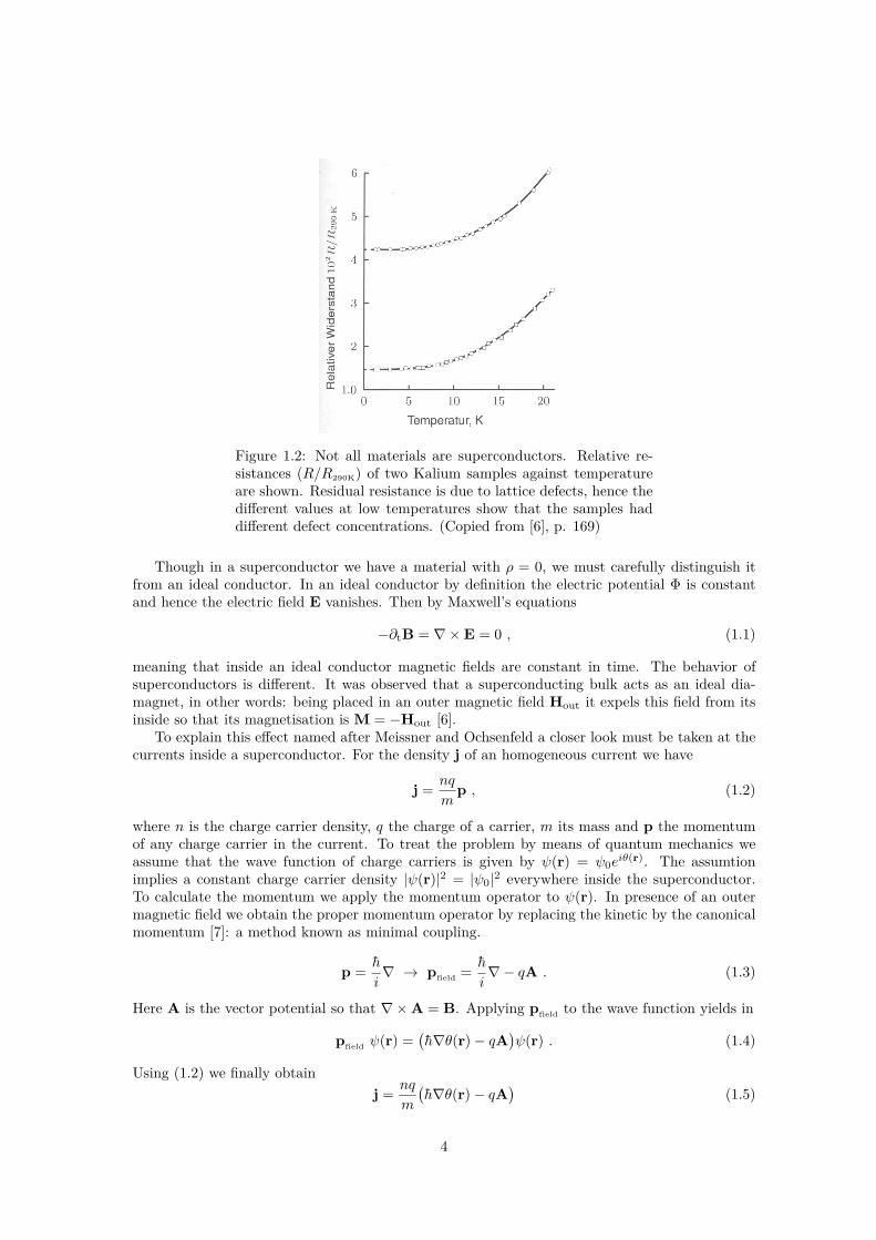
Figure 1.2: Not all materials are superconductors. Relative re-sistances (R/R290K) of two Kalium samples against temperatureare shown. Residual resistance is due to lattice defects, hence thedifferent values at low temperatures show that the samples haddifferent defect concentrations. (Copied from [6], p. 169)
Though in a superconductor we have a material with ρ = 0, we must carefully distinguish itfrom an ideal conductor. In an ideal conductor by definition the electric potential Φ is constantand hence the electric field E vanishes. Then by Maxwell’s equations
−∂tB = ∇ × E = 0 , (1.1)
meaning that inside an ideal conductor magnetic fields are constant in time. The behavior ofsuperconductors is different. It was observed that a superconducting bulk acts as an ideal dia-magnet, in other words: being placed in an outer magnetic field Hout it expels this field from itsinside so that its magnetisation is M = −Hout [6].
To explain this effect named after Meissner and Ochsenfeld a closer look must be taken at thecurrents inside a superconductor. For the density j of an homogeneous current we have
j =nq
mp , (1.2)
where n is the charge carrier density, q the charge of a carrier, m its mass and p the momentumof any charge carrier in the current. To treat the problem by means of quantum mechanics weassume that the wave function of charge carriers is given by ψ(r) = ψ0e
iθ(r). The assumtionimplies a constant charge carrier density |ψ(r)|2 = |ψ0|2 everywhere inside the superconductor.To calculate the momentum we apply the momentum operator to ψ(r). In presence of an outermagnetic field we obtain the proper momentum operator by replacing the kinetic by the canonicalmomentum [7]: a method known as minimal coupling.
p =h
i∇ → p
field=h
i∇ − qA . (1.3)
Here A is the vector potential so that ∇ × A = B. Applying pfield
to the wave function yields in
pfield
ψ(r) =(
h∇θ(r) − qA)
ψ(r) . (1.4)
Using (1.2) we finally obtain
j =nq
m
(
h∇θ(r) − qA)
(1.5)
4

and taking the curl of both sides:
∇ × j = −nq2
mB , (1.6)
because the curl of a gradient field vanishes. Equation 1.6 is called the first London equation. Itoffers the following explanation to the Meissner-Ochsenfeld effect: Since by a Maxwell equation∇×B = µ0j+µ0ǫ0∂tE and in our case there will be no time dependent electric fields, it is ∇×
(
∇×B
)
= −∇2B = − µ0nq2
m B. This equation is called second London equation and(
µ0nq2
m
)−1/2= λ is
called the London penetration depth. The equation indicates that superconductors expel magneticfields, which can be shown by solving it for the simple case of a planar superconducting bulk ofthickness d, placed parallel to the field lines of an homogeneous magnetic field. Disregarding edgeeffects the above equation can be simplified to ∂2
xB = λ−1B, where the x axis lies perpendicularto the bulk surface at x = 0. Then B = Bx=0e
−x/λ meaning that if λ ≪ d inside the bulk B = 0holds. Since B = µ0(Hout +M) we have Hout = −M as quoted above or in terms of susceptibilityχ = −1.
Figure 1.3: Illustration of the behavior of an homogeneous mag-netic field inside a superconductor. The field is parallel to thesuperconductor surface, the field strength decreases exponentiallyas described by the second London equation. (Copied from [8])
Common values for λ are of the order of tens of nm, so that a bulk superconductor will behave asan ideal diamagnet. Figure 1.4 illustrates the difference in behavior of ideal and superconductors.
Figure 1.4: Behavior of a hypothetical material becoming an idealconductor below a critical temperature TC (top) and a supercon-ductor with the same TC (bottom). Inside an ideal conductormagnetic fields do not change with time, whereas the supercon-ductor shows the Meissner Ochsenfeld effect and expels the field.(Copied from [9], p. 457)
5

One consequence of the Meissner-Ochsenfeld effect is that superconducting currents flow on thesurface of a superconductor, otherwise magnetic fields inside the superconductor would appear. Infact it can be shown by further application of Maxwell’s equations that an electric field E inside
the superconductor also has to obay the equation ∇2E = − µ0nq2
m E [10].It is essential to our discussion, that we considered superconducting charge carriers to be
of bosonic nature. Otherwise in the above derivation further complications due to Fermi-Diracstatistics would arise. For example in case of fermionic charge carriers it is known that only thosecarriers located on the Fermi surface can support an electric current. As we will see supercon-ducting charge carriers in fact are bosonic.
1.2 Flux Quantization, Classification of Superconductors in
Types I and II, BCS Theory
1.2.1 Flux Quantization
The magnetic flux through a superconducting ring (see Fig. 1.5) is quantized in whole numbermultiples of the flux quantum Φ0 = h
q , where h denotes Planck’s constant and q is the charge ofa single superconducting charge carrier. In other words: flux is quantized. This can be explainedusing equation (1.5). As discussed in section 1.1 inside the superconductor no currents flow. From(1.5) we get ∇θ = q
h A and integrating over the closed loop C (Fig. 1.5) yields:
∮
c
∇θds =q
h
∮
c
A · ds . (1.7)
Stokes’ theorem together with ∇ × A = B gives
∮
c
∇θds =q
h
∫
B · ds , (1.8)
where the second integral is over the inner surface of the ring and gives the total flux through thering. The first integral, if not carried out over the whole loop, but between the two points 1 and
2 gives:∫ 2
1∇θds = θ2 − θ1. For a well behaved θ(r) the closed integral should vanish. However
it is not of physical importance that θ(r) is well behaved, but that eiθ(r) is well defined at everypoint r
∮
c
∇θds = 2πn (1.9)
holds, where n is an integer number1. Obviously under such a condition eiθ(r) is well defined atthe point r0. On the other hand
∮
c∇θds = 2πn 6= 0 becomes possible. Putting eq. (1.9) and
eq. (1.8) together we see, that if the total flux inside the ring Φ =∫
B · ds does not vanish, it isnecessarily
Φ =2πhn
q=h
qn (1.10)
and flux is quantized. Figure 1.6 shows a measurement of quantized flux.
1If we are not too concerned with uniqueness of θ at every point, a function satisfying (1.9) is not hard to find.For example θ = φ, where φ is the polar angle, satisfies (1.9).
6

Figure 1.5: Magnetic flux inside a superconducting ring. The areathrough which the flux flows is not superconducting. Integrationpath C is shown. ([6], p. 308)
Figure 1.6: Measurement of magnetic flux quantization in a Sncylinder. Flux comes in quanta of Φ0 = h
2e . ([11], p. 30)
1.2.2 Type I and Type II Superconductors
Type I and type II superconductors show different magnetisation properties. A type I supercon-ductor expels an applied magnetic field completely until it reaches a critical value HC . Above HC
the material shows no superconductivity. A type II superconductor expels an applied magneticfield completely until it reaches a critical value HC1. Above HC1 the magnetic field is expelledonly partly. This state is called the vortex state. Finally above a second critical value HC2 thesuperconductivity vanishes. Figure 1.7 visualizes this behavior.
Figure 1.7: Magnetization depending on applied outer magneticfield H. In Type 1 materials superconductivity breaks down at acritical field Hc. In Type 2 superconductors above Hc1 magneticfields are expelled only partly. Here superconductivity breaksdown at a higher outer field Hc2 (after [12])
.
7

Typically HC and HC1 are quite low and HC1 ≪ HC2. To distinguish between both supercon-ductor types more precisely the coherence length ξ must be introduced. It is the length beneathwhich electromagnetic fields varying in space have no considerable influence on superconductingcharge carrier density. Hence to calculate j fields must be averaged over ξ. Later ξ will be definedmore carefully. As stated in [6] following distinction can be made: London penetration depthλ < ξ for a type I superconductor, whereas λ > ξ for a type II superconductor.
An important property of Type II superconductors is that between HC1 and HC2 magneticfields can penetrate the superconductor in the form of so called Abrikosov vortices (hence M 6=−Hout and the name vortex state). This is visualized in Figure 1.8. Inside a vortex the materialis not in the superconducting but in the normal conducting state, hence flux quantization occursand the flux inside a vortex is equal to Φ0. In presence of an electric field vortices can move insidethe superconductor dissipating energy, however they tend to pin on crystal defects. To lower theenergy dissipation due to Abrikosov vortices on a superconducting film so called pinning centersor flux traps, consisting of non-superconducting areas acting as artificial defects, can be placed(see section 3.1).
Figure 1.8: In a Type II superconductor an applied outer mag-netic field penetrates the superconductor in the form of so calledAbrikosov vortices. Inside the vortices material is not supercon-ducting, hence flux quantization occurs. Every vortex carries onquantum of magnetic flux. Supercurrents supporting the flux areshown. ([13], p. 24)
1.2.3 BCS-Theory
The accepted microscopic theory on conventional superconductivity is the BCS (Bardeen, Cooper,Schrieffer) theory. It states that even a weak attractive force between electrons leads to an elec-tronic energy ground state of electrons (BCS groundstate) that is separated from excited statesby an energy gap of size ∆ and lies below the Fermi level of ordinary electrons.
Attractive forces between electrons stem from scattered electrons deforming the lattice andmaking it possible for another electron to use this deformation to minimize its potential energy.The two electrons are then attracted to each other. This attraction can be described mathemati-cally by the exchange of a (virtual) phonon between the two electrons (see Fig. 1.9). One mightwonder, why the Coulomb force does not destroy such a subtle interaction. Here it is of impor-tance that the processes of lattice deformation and Coulomb force act on significantly differenttimescales. The time the lattice takes to return to its original state is so long, that the scatteredelectron already is “too far away” for the Coulomb interaction between it and the arriving secondelectron to be of importance.
8

Figure 1.9: A Cooper pair. Two electrons with opposite momen-tum vectors are attracted by means of a virtual phonon exchange.Cooper pairs are the charge carriers of supercurrent. ([13], p. 117)
The attracted electrons as shown in Fig. 1.9 are called Cooper pairs. Electrons of a Cooperpair have wave vectors k, −k and, which is most important, spins (↑) showing in oposite directions(see [13], p. 115). Therefore Cooper pairs k ↑,−k ↓ are bosonic and can condense in the BCSgroundstate. Measurements of quantized flux (Φ0 = h
q ) show ([6], p. 308) that the charge qof superconducting charge carriers is in fact −2e, meaning that supercurrents are supported byCooper pairs.
Many electromagnetic properties of superconductors are consequences of the existance of theenergy gap ∆. Cooper pairs can not be decelerated by scattering on lattice defects, because thereexist no energy states supporting such a process. The occurance of critical temperature TC alsois explained by ∆. Furthermore the BCS theory delivers a formula for coherence length ξ0 =2hvF /π∆ ([6], p.306), where vF is the Fermi velocity. In case of so called dirty superconductorswith mean free path l for electrons in the normal state it is ξ = (ξ0 · l)1/2, which together with1.2.2 explains why alloys and non-epitaxial thin films tend to be type II superconductors. Forexample pure lead is a type I superconductor, whereas an alloy of lead and 2% Indium becomestype II. NbN films, used for resonator fabrication in our case, also are type II superconductors.
1.3 Kinetic inductance
The energy stored in a magnetic field H,B is given by W = 12
∫
VH · B d3x. For a wire through
which current I flows W can also be expressed in terms of current [14]:
W =1
2LgeoI
2 , (1.11)
where Lgeo is called inductance and depends on the geometry (curvature, length...) of the wire.Creating a magnetic field is not the only way a flowing current can store energy. The kineticenergy of charge carriers also can be of importance, however it is negligible for a normal conductorsince, due to frequent scattering, electrons have no time to accumulate a great amount of kineticenergy beside their thermal energy which is not considered, because it is not caused by an electricfield. Cooper pairs however are not scattered and therefore can store kinetic energy.
Consider a thin superconducting film of cross section A and length l with a homogeneouscurrent density j. The total current is I = jA. The kinetic energy stored by the current is
Ekin =∑ p2
2m where the sum is over all Cooper pairs. Assuming an homogeneous Cooper pair
density ns we can write Ekin = p2
2m · ns · A · l. From (1.2) we get p = mnsq j and therefore using
9

I = jA:
Ekin =m
2nsq2
l
AI2 . (1.12)
Since Ekin ∝ I2 in analogy to (1.11) we can write
Ekin =1
2LkinI
2 (1.13)
hereby defining the kinetic inductance Lkin. The total energy stored is Etot = Ekin +W = 12
(
Lkin +
Lgeo
)
I2. Therefore total inductance is the sum of geometric and kinetic inductance. From thisfollows, that geometric and kinetic inductance behave equal in terms of ac impedances. Theresonant frequency 1/
√LC of an ordinary capacitance inductance resonator is lowered by a non
vanishing kinetic inductance because of L = Lgeo + Lkin.
10
Chapter 2
Resonator Theory
This chapter gives an overview of lumped element resonator theory. Scattering parameters aredefined and discussed, as well as parallel, series RLC resonators and their quality factors. A lumpedelements model of a spiral resonator capacitively coupled to a feedline is proposed. Methodes fordetermining quality factors from simulations are derived from the model.
2.1 The Transmission Line
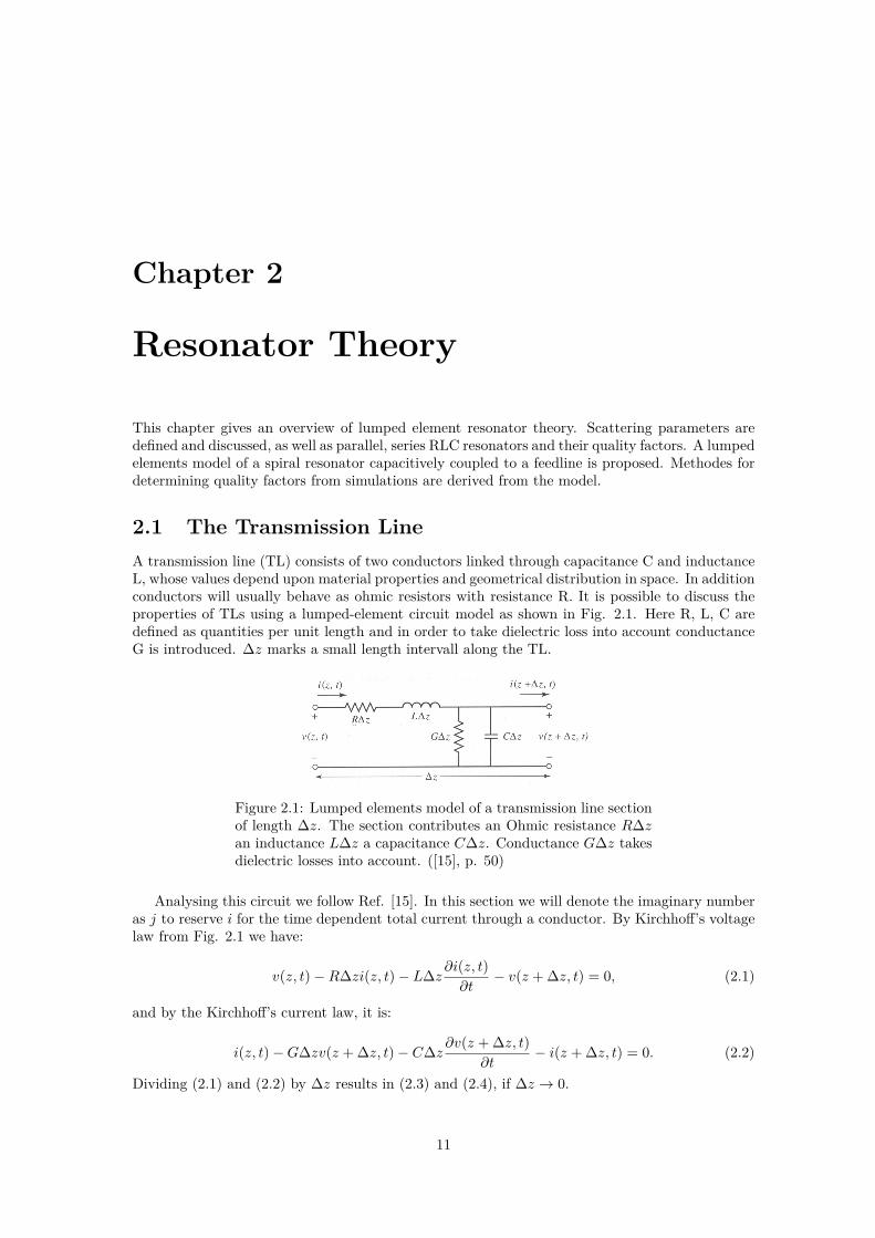
A transmission line (TL) consists of two conductors linked through capacitance C and inductanceL, whose values depend upon material properties and geometrical distribution in space. In additionconductors will usually behave as ohmic resistors with resistance R. It is possible to discuss theproperties of TLs using a lumped-element circuit model as shown in Fig. 2.1. Here R, L, C aredefined as quantities per unit length and in order to take dielectric loss into account conductanceG is introduced. ∆z marks a small length intervall along the TL.
Figure 2.1: Lumped elements model of a transmission line sectionof length ∆z. The section contributes an Ohmic resistance R∆zan inductance L∆z a capacitance C∆z. Conductance G∆z takesdielectric losses into account. ([15], p. 50)
Analysing this circuit we follow Ref. [15]. In this section we will denote the imaginary numberas j to reserve i for the time dependent total current through a conductor. By Kirchhoff’s voltagelaw from Fig. 2.1 we have:
v(z, t) −R∆zi(z, t) − L∆z∂i(z, t)
∂t− v(z + ∆z, t) = 0, (2.1)
and by the Kirchhoff’s current law, it is:
i(z, t) −G∆zv(z + ∆z, t) − C∆z∂v(z + ∆z, t)
∂t− i(z + ∆z, t) = 0. (2.2)
Dividing (2.1) and (2.2) by ∆z results in (2.3) and (2.4), if ∆z → 0.
11

∂v(z, t)
∂z= −Ri(z, t) − L
i(z, t)
∂t(2.3)
∂i(z, t)
∂z= −Gv(z, t) − L
v(z, t)
∂t. (2.4)
Assuming oscillating voltages and currents v(z, t) = V (z)ejωt and i(z, t) = I(z)ejωt (2.3) and (2.4)can be rewritten as
dV
dz= −(R+ jωL)I (2.5)
dI
dz= −(G+ jωC)V . (2.6)
General solutions to this first order coupled ordinary differential equations are
V (z) = V +0 e−γz + V −
0 eγz (2.7)
I(z) = I+0 e
−γz + I−0 e
γz , (2.8)
implying that wave propagation is possible in +z direction (hence V +0 , I+
0 ) and -z direction.
γ =√
(R+ jwL)(G+ jwC) = α+ jβ is called propagation constant. By plugging (2.7) into (2.5)we see that
I(z) = Z0
(
V +0 e−γz − V −
0 eγz)
, (2.9)
where Z0 = γR+jωL is called characteristic impedance.
2.1.1 Reflection and Transmission Coefficients
In this section we assume a low loss or lossless transmission line, so that the amplitudes of voltageand current are constant along the TL. Consider a terminated TL as shown in Fig. 2.2. By
definition it is ZL = V (z=0)I(z=0) . From (2.7), (2.9) we see ZL =
V +0
+V −
0
V +0
−V −
0
Z0, so that
V −0
V +0
=ZL − Z0
ZL + Z0=: Γ . (2.10)
The ratio between amplitudes of incident and reflected waves Γ is called reflection coefficient. Notethat Γ = 0 if ZL = Z0, so no waves are reflected.
Figure 2.2: Transmission line with characteristic impedance Z0
and propagation constant jβ terminated at z = 0 in an impedanceZL. ([15], p.58)
To calculate the transmission coefficient T we imagine that the TL is not terminated at z = 0 butconnected to another TL with a different characteristic impedance Z1 (Fig. 2.3).
12

Figure 2.3: Illustration of transmission and reflection of waves ata connection of TLs of different characteristic impedances. ([15],p.63)
(2.7) can be rewritten as V (z) = V +0
(
e−jγz + Γejγz)
. Assuming the second TL is terminatedin Z1 somewhere at z > 0, there is no reflection except at z = 0. Thus for z > 0 we writeV1(z) = V +
0 Te−γz, hereby defining the transmission coefficient T. At z = 0 it is V (0) = V1(0), sothat
T = 1 + Γ =2Z1
Z1 + Z0. (2.11)
2.2 Scattering Parameters of a Two Port
During this work a spiral resonator coupled to a feedline is considered to be a two port network.Abstractly speaking a two port networt (short: two port) consists of a “black box”1 and fourterminals (see Fig. 2.4). Two terminals respectively form a port, which can be connected to a TL.
Figure 2.4: An abstract two port. V+/−
i are the amplitudes ofincident or reflected voltage waves. The black box may containsome unknown circuitry.
The so called scattering parameters can be defined by
Sij =V −
i
V +j
, (2.12)
where i, j indicate at which port voltage amplitude is measured and where - / + indicate the am-plitude of waves leaving / entering the “black box”. In our case the “black box” has an impedanceZbox and the TL leading to port 2 is terminated in an impedance that equals its characteristicimpedance Z0, to avoid wave reflection at the port (see Fig. 2.5).
1in our case containing the resonator
13

Figure 2.5: In simulations we will concider a two port where one ofthe ports is terminated to avoid wave reflections. The scatteringparameters are calculated taking this termination into account.
Effectivly such a two port is a TL2 with characteristic impedance Z0 terminated in an impedanceZeff. Depending on the box circuitry it is Zeff = Zbox + Z0 or Zeff = Zbox||Z0. The symbol a||bstands for a and b being cirquited parallel. Now the expressions for the scattering parameters canbe obtained in terms of impedances. By (2.10) and (2.11) we know that
S11 = Γ =Zeff − Z0
Zeff + Z0(2.13)
and
S21 = T =2Zeff
Zeff + Z0. (2.14)
2.3 Resonant Circuits and Quality Factors
2.3.1 Series RLC Resonant Circuit
A series RLC is shown in Fig. 2.8. Its input impedance is Zin = R+ jωL+ 1jωC and the resonance
frequency is ω0 = 1√LC
, implying that |Zin| at resonance is minimal and Zin(ω0) = R is real.
Figure 2.6: Series RLC contour consisting of resistor R, induc-tance L and capacitance C.
An important parameter of a resonant cirquit is its quality factor Q, indicating how well thecirquit stores energy. It is defined as
Q = ωaverage energy stored
energy loss per time unit= ω
Wm +We
Pl, (2.15)
where Wm = 14 |I|2L is the average energy stored in magnetic fields, We = 1
4 |VC |2C = 14 |I|2 1
ω2Cthe average energy stored in electric fields and Pl = 1
2 |I|2R the average power dissipated. Theadditional factor 1
2 in this equations origins in averaging over the sinusoidal time dependences ofI and V . Plugging this into (2.15) gives Qω0
= 1ω0RC .
For a small ∆ω = w − w0 the impedance of a series RLC can be approximated by
Zin ≈ R+ j2RQ∆ω
ω0= R+ j2L∆ω . (2.16)
Using this result it can be shown3 that
Q ≈ ω0
BWω, (2.17)
2namely the TL leading to port 1.3See [15], p. 268f for further details.
14

where BWω is the width of |Zin|-curve at |Zin| = 1√2R (see Fig. 2.7). This approximation is
reasonable for large quality factors, where ∆ω is small.
Figure 2.7: Input impedance of a series RLC. Illustration of de-terming Qi by measuring the width of |Zin|-curve. ([15], p.267)
2.3.2 Parallel RLC Resonant Circuit
The input impedance of a parallel RLC circuit is given by |Zin| = 11R
+ 1jωL
+jωC, its resonant
frequency is ω0 = 1√LC
and its quality factor is Q = ω0RC. For a small ∆ω = w − w0 the
impedance can be approximated by
Zin ≈ R
1 + 2j∆ωRC=
R
1 + 2jQ∆ω/ω0, (2.18)
At resonance |Zin| is maximal, but the approximation
Q ≈ ω0
BWω, (2.19)
still holds for a big Q4. The knowledge of parallel and series RLCs is useful, because many resonantcircuits can be approximated by RLCs near resonance.
Figure 2.8: Parallel RLC contour consisting of resistor R, induc-tance L and capacitance C.
Until now only the internal energy loss of resonators was concidered, usually however theresonator is coupled to other circuitry, which lowers its overall Q. Let Qi be the resonator’sinternal quality factor. We define the coupling quality factor Qc such, that
1
Q=
1
Qc+
1
Qi. (2.20)
4See [15], p. 270f for further details.
15

2.4 Lumped Element Model of a Spiral Resonator Coupled
to a Feedline
Naively one can picture a spiral resonator (Fig. 2.10) as a wound up piece of open-cirquitedTL (Fig. 2.9). An open circuited piece of TL behaves as a resonator by itself and its inputimpedance can be, at resonance, approximated5 by Zin ≈ Z0
αl+j(∆ωπ/ω0) . Here α is the real part
of propagation constant γ, l the TL’s length and Z0 its characteristic impedance. Comparing thisexpression for Zin to (2.18) we see, that at resonance an open circuited transmission line resonatorbehaves like a parallel RLC circuit. We therefore want to assume that the spiral, being a woundup open circuited TL, also will behave as a parallel RLC at resonance. Additionally the spiral iscapacitively coupled to a feedline6.
Figure 2.9: An open cirquited piece of transmission line with char-acteristic impedance Z0 and propagation constant γ = a + ib asshown here is by itself a resonator. It is resonable to concider aspiral resonator to be a wound up piece of an open circuited TLas done in our analysis. ([15], p.276)
Since in our simulations resonators are considered lossless, the resistance of the parallel RLCapproaches infinity and can be neglected, thus leading to the lumped element model shown in Fig.2.10.
5See [15] p. 276.6Our approach is analogous to the one proposed in Ref. [16], where a waveguide resonator measured in trans-
mission was concidered.
16
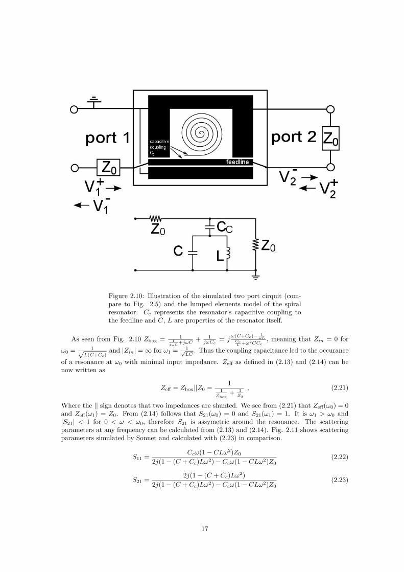
Figure 2.10: Illustration of the simulated two port cirquit (com-pare to Fig. 2.5) and the lumped elements model of the spiralresonator. Cc represents the resonator’s capacitive coupling tothe feedline and C, L are properties of the resonator itself.
As seen from Fig. 2.10 Zbox = 11
jωL+jωC
+ 1jωCc
= jω(C+Cc)− 1
ωLCcL
+ω2CCc
, meaning that Zin = 0 for
ω0 = 1√L(C+Cc)
and |Zin| = ∞ for ω1 = 1√LC
. Thus the coupling capacitance led to the occurance
of a resonance at ω0 with minimal input impedance. Zeff as defined in (2.13) and (2.14) can benow written as
Zeff = Zbox||Z0 =1
1Zbox
+ 1Z0
, (2.21)
Where the || sign denotes that two impedances are shunted. We see from (2.21) that Zeff(ω0) = 0and Zeff(ω1) = Z0. From (2.14) follows that S21(ω0) = 0 and S21(ω1) = 1. It is ω1 > ω0 and|S21| < 1 for 0 < ω < ω0, therefore S21 is assymetric around the resonance. The scatteringparameters at any frequency can be calculated from (2.13) and (2.14). Fig. 2.11 shows scatteringparameters simulated by Sonnet and calculated with (2.23) in comparison.
S11 =Ccω(1 − CLω2)Z0
2j(1 − (C + Cc)Lω2) − Ccω(1 − CLω2)Z0(2.22)
S21 =2j(1 − (C + Cc)Lω2)
2j(1 − (C + Cc)Lω2) − Ccω(1 − CLω2)Z0(2.23)
17

Figure 2.11: Typical |S21| values deliverd by a Sonnet simulationand the fitted |S21|-curve of the lumped elements model. Thelarge figure shows the assymetric behavior at |S21| ≈ 1 due tothe capacitive coupling, and the smaller figure shows the wholeresonance. At ω0 |S21| vanishes, whereas at ω1 |S21| = 1.
The minimum at ω0 in Fig. 2.11 implies, that around this frequency Zeff, representing the cou-pled resonator, can be approximated by the impedance of a series RLC. In fact Taylor expandingZeff gives
Zeff ≈ j 2(C + Cc)2
C2c
L∆ω + O(∆ω2) , (2.24)
which can be written in a form similar to (2.16) by defining Leff = (C+Cc)2
C2c
L.
2.5 Determinating Quality Factors from Simulated Data
The results of preceding analysis are useful for determinating quality factors of spiral resonatorsfrom data obtained by Sonnet simulations.
2.5.1 The -3 dB Method
We first show that a statement resembling (2.17) is valid for our capacitively coupled resonators7.We will, however, concider the absolute value of scattering parameter |S21| instead of the inputimpedance, since simulation data is delivered in form of scattering paramenters. The couplingquality factor at frequency ω0 = 1√
(C+Cc)Lcan be calculated using the lumped element model
(Fig. 2.13) and is given by
Qc = ω0Wm +We
Pl= ω0
|VC |2
4ω20
L+ 1
4 |VC |2C + 14 |VCc
|2Cc
|VZ0|2/Z0
= 2(C + Cc)
√
(C + Cc)L
C2cZ0
. (2.25)
From (2.14) and (2.21) it is |S21|2 =[
1 +C2
c ω2(CLω2−1)2Z20
4((C+Cc)Lω2−1)2
]−1=
[
1 + 14Y
]−1. Let BWω be the
width of |S21|-curve at the point where Q ≈ ω0
BWω. Approximating ω2 = (ω0 +∆ω)2 ≈ ω2
0 +2ω0∆ω
7This is reasonable because the coupled resonator, in contrary to the uncoupled spiral, can be approximated asseries RLC, as shown in 2.24.
18

for a small ∆ω = 12BWω we can write Y =
(QC2c Z0−CCcZ0)2(QC2
c Z0+C2c Z0)
14
Q3C6c Z3
0
= 4(
1 + O(
1Q
)
)
, which
is effectively 4 for a big Q. Thus |S21| = 1√2
when Q ≈ ω0
BWω
Since Q ≈ ω0
BWωat |S21| = 1√
2one can determine Q by measuring BWω and resonance
frequency ω0. In case scattering parameters are given in dB, |S21|2 = 12 corresponds |S21| =
−3dB. This method however often is tedious because BWω can be measured properly only afterperforming several “zoom-in” simulations.
Figure 2.12: Model used for calculating the Q factor. The calcu-lation implies that voltage is applied at capacitance C at t = 0,power passing through Cc at t > 0 is dissipated.
Figure 2.13: Measuring the the width of the resonance allowsto determine the quality factors of a resonator. Measuring thewidth 3dB below |S21| = 1 gives the overall, loaded Q. It isQ = ω0
BW1, where ω0 is the resonance frequency and BW the width.
Through measuring the width 3dB above the resonance minimumone obtains the internal quality factor Qi = ω0
BW2(see 2.3.1). Since
in this chapter we are considering a lossless resonator, power onlydissipates through the coupling to cirquitry and the quality factorcorresponding to BW1 is the coupling quality factor Qc = Q (see(2.20)).
19
2.5.2 Determination of Q through linearization of S21
Near ω0 |S21| behaves linear and can be approximated by
|S21| = 4(C + Cc)2L
C22Z0∆ω + O(∆ω2) = 2Q
∆ω
ω0+ O(∆ω2) . (2.26)
If therefore a simulation delivers some |S21|-values near zero, the Q factor can be determined from(2.26).
2.5.3 Determination of Q Using a Third Port
Additionally, as shown in Ref. [17], Q can be determined using a third port directly attached tothe resonating part of the circuit (Fig. 2.14). The third port allows to measure the resonator’sinput impedance. Although in simulations resonators are assumed lossless, their input impedanceZin can be approximated by that of parallel or series RLC with finite R due to energy dissipationthrough their coupling to feedlines. Ref. [17] conciders the series RLC case, where from (2.16)
one sees immediately that ℜ(Zin) = R and dℑ(Zin)dω = 2RQ
ω0. This is not obvious for the parallel
RLC circuit representing a resonating spiral, however Taylor expanding (2.18) around ω0 showsthat here Zin = R − j 2RQ
ω0∆ω. In both cases Q can be determined from ℜ(Zin) and the slope
S = dℑ(Zin)dω at resonance.
R = ℜ(Zin(ω0)) (2.27)
Q =∣
∣
∣
Sω0
2R
∣
∣
∣. (2.28)
All three methods were used during this work. If carried out properly the results of all threemethods are in good agreement with each other (see Table 2.1).
20

Method Qc
-3 dB 2330 ± 30Linearization 2324 ± 5Third port 2330 ± 5
Table 2.1: The quality factor of a resonator at 6.52 GHz wasdetermined using the three described methods. The results werein good agreement.
Figure 2.14: Geometry of a Sonnet simulation using three ports.
21

Chapter 3
Design and Simulation of Spiral
Resonators
3.1 Spiral Design
Two types of resonating spirals were chosen to be investigated during this work. First a simpleArchimedean and second a double wound spiral (Fig. 3.1). The layouts were created with LEdit[18], a programm commonly used for designing MEMS, which allows to generate circuit geometryfrom C++ code. To parameterize the Archimedean spiral the formula
~r(t) = R(t)
(
cos(ωt)sin(ωt)
)
(3.1)
was used. R(t) is a function linear in t. Through a convenient choice of R(t) and ω, dependingon the width of spiral loops as well as on outer and inner radii, one obtains a spiral with a givennumber of loops n. Parameters used to describe the spirals are listed and explained in Fig. 3.2.Double wound spirals were constructed out of two Archimedean spirals, whose centers were shiftedagainst each other and connected with two half open toruses.
Figure 3.1: Two types of spiral resonators were simulated: a sim-ple Archimedean spiral and a double wound spiral as seen on theright.
In total 32 resonators of different resonant frequencies, quality factors and widths of spiralloops were designed. The resonators were distributed on four chips, with eight resonators on each.
22

All resonators on one chip differ in frequencies but are of the same type (simple or double wound).Four of the resonators on each chip have a high coupling Q (order of 105) and four have a low one(order of 103). Table 3.1 lists all the resonators and chips.
Chip Resonant frequency Type of spiral Width of spiral loops Qc
SPIRAL S 1 15 GHz simple Archimedean 1µm ≈ 103
6 GHz ” ” ”7 GHz ” ” ”8 GHz ” ” ”5.25 GHz ” ” ≈ 105
6.25 GHz ” ” ”7.25 GHz ” ” ”8.25 GHz ” ” ”
SPIRAL S 5 55 GHz simple Archimedean 5µm ≈ 103
6 GHz ” ” ”7 GHz ” ” ”8 GHz ” ” ”5.25 GHz ” ” ≈ 105
6.25 GHz ” ” ”7.25 GHz ” ” ”8.25 GHz ” ” ”
SPIRAL D 1 15 GHz double wound 1µm ≈ 103
6 GHz ” ” ”7 GHz ” ” ”8 GHz ” ” ”5.25 GHz ” ” ≈ 105
6.25 GHz ” ” ”7.25 GHz ” ” ”8.25 GHz ” ” ”
SPIRAL D 5 55 GHz double wound 5µm ≈ 103
6 GHz ” ” ”7 GHz ” ” ”8 GHz ” ” ”5.25 GHz ” ” ≈ 105
6.25 GHz ” ” ”7.25 GHz ” ” ”8.25 GHz ” ” ”
Table 3.1: Table of the 32 designed resonators and their charac-teristics. The chip names are as written on the chips themselves;S/D meaning simple or double, 1 1 and 5 5 indicating the widthof spiral loops and distance between loops in µm.
23

Figure 3.2: Parameters used to specify a spiral resonator’s geom-etry. loopn: number of loops, polyt: number of vertices of thespiral polygon. rad0: outer radius, width: width of spiral loops,distance: distance between spiral loops. feedline distance: dis-tance between spiral coupling and feedline or bridge. coupling:length of spiral’s capacitive coupling. bridge: whether a groundedbridge between feedline and spiral is placed to achieve a higherQc. anglecutoff: angle to be cut off at the inner end of the spiralto fine tune the resonant frequency.
The quality factor Qc as calculated from the lumped elements model (see 2.5) is given by
Qc = 2(C + Cc)
√
(C + Cc)L
C2cZ0
, (3.2)
meaning that we can adjust Qc by varying the coupling capacity Cc. To do so it is possible tovary the distance between coupling and feedline d or the length of the couling l - analogous toa parallel-plate capacitor. Aditionally to achieve a higher Qc a grounded bridge of width w canbe placed between coupling and feedline (for typical values of d, l and w see table 3.1). In caseof our resonators Cc was adjusted once at a certain frequency for a certain type of spiral (simpleor double wound design, 5 or 1 µm loop width, coupling strength) and then kept while varyingfrequency. Thus the Qc of resonators with same coupling geometry but different frequencies variesby a factor of two to three, which is not surprising, since, to vary the frequency from 5GHz to8GHz the resonator’s geometry, i.e. C and L have to be changed.
24

Type of Resonator Resesonance Coupling Qc Width offrequency /GHz length /µm grounded
bridge /µm
Simple Archimedean 8.2 6 670 0Simple Archimedean 8.2 26 10500 15Double wound 8.3 1 5000 0Double wound 8.3 8 11000 1
Table 3.2: Data on coupling length, width of grounded bridgebetween feedline and coupling as well as distance between feedlineand coupling for simple Archimedean and double wound types ofresonators with a loop width of 1µm.
Altering the radius as well as the number of loops and thereby it’s length changes the resonancefrequency of a spiral resonator. Facing the task of designing 32 resonators with given frequenciesit seems reasonable to change only one of the many spiral parameters from Fig. 3.2. The decisionwas made to let the number of loops constant for a certain type of spiral and to alter the frequencyby changing the outer radius. Since the width of spiral loops was fixed to 1 or 5 µm altering theouter radius automatically leads to an altered inner radius, which is not an independent parameterin our design (see Fig. 3.3).
Figure 3.3: To vary the resonant frequencies, outer radii of thespirals were changed, whereas the number of loops was held con-stant. The figure shows resonators at 8.25, 6.25 and 5.25 GHz.
Finally, for each type of spiral, frequencies were adjusted in the same way. Four outer radiiwere chosen by eye, simulated and than, through an interpolation of obtained results, radii corre-sponding to the required frequencies were calculated. As an example we show how the frequenciesof the four double wound resonators with a loop width of 5µm and Qcof order 105 were adjusted.Here simulations yielded in the results shown in table 3.3.
Outer radius /µm Resonant frequency /GHz
159 8.36180 6.56198 5.53212 4.93
Table 3.3: Results of simulations of four double wound resonatorswith a loop width of 5µm and different outer radii.
This data was interpolated with a polynomial of fourth degree:
router = 509µm − 106µm
GHzν + 11.7
µm
GHz2 ν2 − 0.478
µm
GHz3 ν3 , (3.3)
which allows to calculate radii leading to needed resonance frequencies (table 3.4).
25

Outer radius /µm Resonant frequency /GHz
204 5.25184 6.25170 7.25159 8.25
Table 3.4: Calculated outer radii of four double wound resonatorswith a loop width of 5µm and Qcof order 105.
Figure 3.4 shows the simulated frequencies and the interpolation polynomial.
5.0 5.5 6.0 6.5 7.0 7.5 8.0Frequency GHz
160
170
180
190
200
210
Outer radius
Figure 3.4: Outer radii in µm and resonance frequencies of fourdouble wound spirals. Simulated frequencies and the interpola-tion polynomial used to determine radii corresponding to givenresonance frequencies.
After designing the resonators in the manner described above they were distributed on chipsaccording to table 3.1. A chip is shown in Fig. 3.6. Although our resonators nominally aremeasured at zero magnetic field, to avoid energy dissipation due to Abrikosov vortices in caseof some residual magnetic field, flux traps were placed on the chips as suggested by Ref. [19].The traps consist of rectangular, 10x10 µm2 large holes in the superconducting film and weredistributed 10µm apart from each other over the whole surface of the chip. No flux traps wereplaced on the spiral itself and the feedline. A strip of 5µm width around the edges of feedlineand resonator box was kept flux trap free to avoid influence on quality factors and resonancefrequencies (Fig. 3.5).
26

Figure 3.5: Rectangular nonconducting flux traps were placed onthe chip’s surface to lower the energy losses due to Abrikosovvortices. The flux traps are 10x10 µm2 in size.
Figure 3.6: Part of a chip consisting of launcher and four res-onators. Eight resonators of the same kind were placed on everychip.
27

Type Radii of 5.0 GHz resonators Radii of 8.0 GHz resonators
Simple 1 1 78 µm 62 µmDouble 1 1 91 µm 70 µmSimple 5 5 178 µm 140 µmDouble 5 5 210 µm 161 µm
Table 3.5: Radii of smallest and largest resonators of every type.
3.2 Simulation of Resonators
To determine the resonance frequency and quality factor of designed resonators the spirals weresimulated with Sonnet [20]. Sonnet is a commercial software, which allows simulations of planarcircuits or antennas at high frequencies. As described in the previous section, in order to obtainprecise resonance frequencies the parameters of a spiral were changed by eye and then simulationresults were interpolated. Simulations were carried out with the two port geometry shown in figure3.7, employing a third port for determining Qc if necessary. The flux traps were not simulated dueto memory constrains, however the grounded planes around spiral and feedline were included. Asthe feedline width was chosen to be 10µm, the distance between feedline and grounded box wasfixed to 6µm ensuring a characteristic transmission line impedance of 50Ω to avoid wave reflectionat the ports.
Figure 3.7: Geometry of Sonnet simulations. Simulation planewith spiral and grounded box consisting of an ideal conductor.Vacuum (ǫr = 1) above and silicon (ǫr = 11) below the simulationplane.
Silicon is used as substrate for resonator chips, so a dielectric constant ǫ = 11 was chosen asmaterial parameter for the layer below and ǫ = 1 for the layer above the superconducting surface(vacuum). The thickness of both layers was chosen to be 1000µm (see Fig. 3.7). All conductingparts were simulated as ideal conductors with zero resistance; dielectric losses were neglected, too.
The results of a simulation are given in terms of scattering parameters Sij or in terms ofimpedances. Being at the minimum of transmission the resonance frequency can be directly seenfrom the S21 data. Qc factors were determined using methods described in the resonator theorychapter. The duration of a simulation strongly depends on the quality factor of a simulatedresonator. For a high Qc resonator it is more difficult to obtain an accurate resonance curve, since
28
the curve is narrow and demands a high resolution in frequency space.
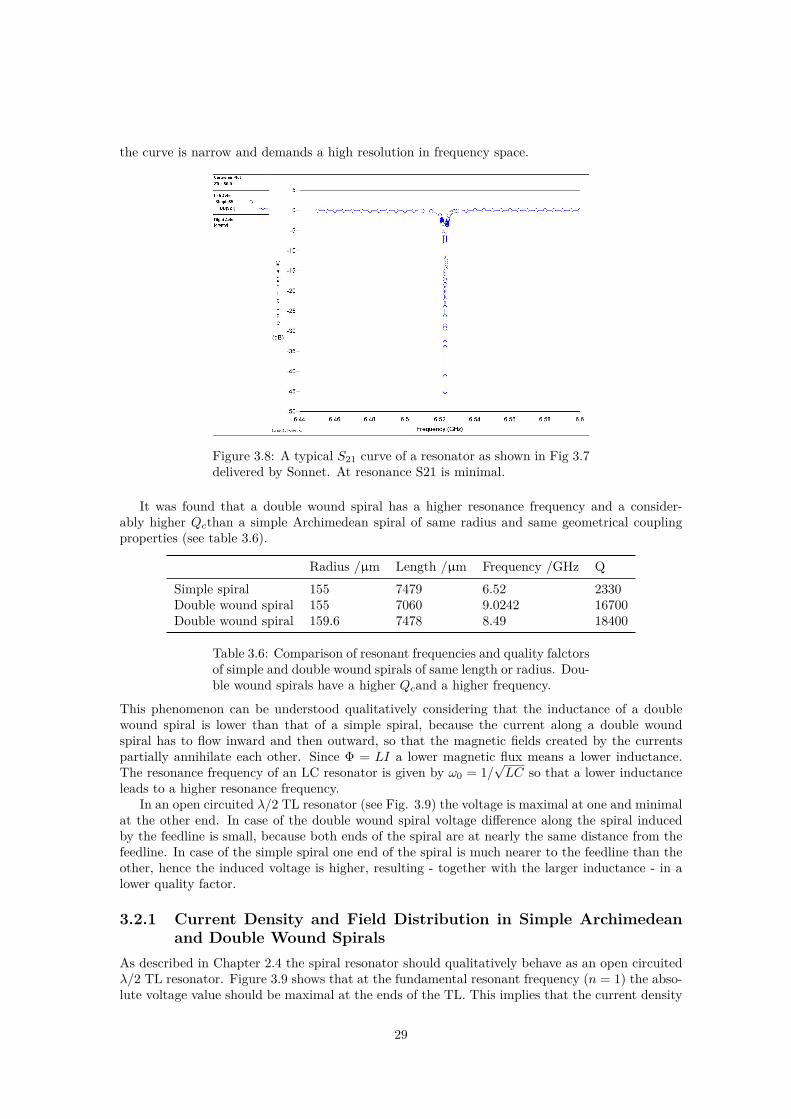
Figure 3.8: A typical S21 curve of a resonator as shown in Fig 3.7delivered by Sonnet. At resonance S21 is minimal.
It was found that a double wound spiral has a higher resonance frequency and a consider-ably higher Qcthan a simple Archimedean spiral of same radius and same geometrical couplingproperties (see table 3.6).
Radius /µm Length /µm Frequency /GHz Q
Simple spiral 155 7479 6.52 2330Double wound spiral 155 7060 9.0242 16700Double wound spiral 159.6 7478 8.49 18400
Table 3.6: Comparison of resonant frequencies and quality falctorsof simple and double wound spirals of same length or radius. Dou-ble wound spirals have a higher Qcand a higher frequency.
This phenomenon can be understood qualitatively considering that the inductance of a doublewound spiral is lower than that of a simple spiral, because the current along a double woundspiral has to flow inward and then outward, so that the magnetic fields created by the currentspartially annihilate each other. Since Φ = LI a lower magnetic flux means a lower inductance.The resonance frequency of an LC resonator is given by ω0 = 1/
√LC so that a lower inductance
leads to a higher resonance frequency.In an open circuited λ/2 TL resonator (see Fig. 3.9) the voltage is maximal at one and minimal
at the other end. In case of the double wound spiral voltage difference along the spiral inducedby the feedline is small, because both ends of the spiral are at nearly the same distance from thefeedline. In case of the simple spiral one end of the spiral is much nearer to the feedline than theother, hence the induced voltage is higher, resulting - together with the larger inductance - in alower quality factor.
3.2.1 Current Density and Field Distribution in Simple Archimedean
and Double Wound Spirals
As described in Chapter 2.4 the spiral resonator should qualitatively behave as an open circuitedλ/2 TL resonator. Figure 3.9 shows that at the fundamental resonant frequency (n = 1) the abso-lute voltage value should be maximal at the ends of the TL. This implies that the current density
29

is minimal at the ends and maximal in the middle (at l/2) of the resonator. In fact simulationsconfirmed that this is the case. Figures 3.10 and 3.11 show the current destributions along simpleand double wound spirals, figures 3.12 and 3.13 show the corresponding field distributions1.
Figure 3.9: Voltage distribution along an open circuited λ/2 TLresonator, which can be used to develop a qualitative understand-ing of the behaviour of the spiral resonator. n=1 stands for thefundamental frequency and n=2 for the second harmonic. Theresonator has a characteristic impedance Z0 = α+ jβ. Note thatthe current density is minimal at the TL’s ends. ([?],S.276)
Figure 3.10: Current destribution along asimple Archimedean spiral at the funda-mental resonance frequency. As expectedfrom comparison with the open circuitedλ/2 TL resonator the current density isminimal at the spiral’s ends. Simulationwas performed with Sonnet.
Figure 3.11: Current destribution alonga double wound spiral at the fundamen-tal resonance frequency. As expected fromcomparison with the open circuited λ/2 TLresonator the current density is minimalat the spiral’s ends. Simulation was per-formed with Sonnet.
1Since Sonnet is designed for planar simulations, only the field component parallel to the spiral plane couldbe simulated. For doing so a so called sense metal plane of high reactance was placed above the resonator. Thesimulated current destribution along the sense metal plane is, by Ohms law E = σj, proportional to the fieldstrength.
30

Figure 3.12: Electric field destribution of asimple spiral resonator. The field is max-imal at both ends of the spiral. Notethat Sonnet is only able to simulate thefield component parallel to the spiral plane.The field is simulated by calculating thecurrent destribution of sense metal planeabove the resonator, hence the absolutevalues in this diagramm are not of partic-ular interest.
Figure 3.13: Electric field destribution of adouble wound spiral resonator. The field ismaximal at both ends of the spiral. Notethat Sonnet is only able to simulate thefield component parallel to the spiral plane.
31

Chapter 4
Measurements
One of the four chip designs was measured at 4.2 K and below. The measured chip containeddouble wound spiral resonators of 5 µm loop width. Resonances were observed and internal aswell as coupling quality factors determined.
4.1 Measurement Setup
4.1.1 Sample Chip
Chip SPIRAL D 5 5 (see 3.1), containing four strongly coupled (QC of order of 103) and fourweakly coupled (QC of order of 105) double wound spiral resonators was measured. The chip wasfabricated using intrinsic Si as substrate on which a 60 nm thick intrinsic NbN superconductingfilm was sputtered. The NbN film was found to have a critical temperature of 9.25 K1. Figures4.1 and 4.2 show a part of the chip and a single double wound resonator.
Figure 4.1: Microscope image of a part of the fabricated SPI-RAL D 5 5 chip with launcher attached to feedline and five doublewound spiral resonators of different frequencies along the feedline.
1Tobias Bier by private communivation.
32

Figure 4.2: A fabricated double wound strongly coupled spiralresonator at 6 GHz. Fluxtraps, 10 x 10 µm2 in size, were placedon the groundplane.
Before measurements the protecting photoresist for dicing was removed from the chip withaceton, isopropanol and ethanol baths. Then the chip was wire-bonded to a cryostatic sampleholder (see Fig. 4.3).
Figure 4.3: The chip’s launcher bonded to the sampleholder withtwo bonding wires.
4.1.2 The Setup
After bonding the sample was attached to a dipstick (Fig. 4.4), covered with a Mu-metal magneticshield and placed inside a helium (4He) Dewar at 4.2 K. The sampleholder at the end of the dipstickwas conncected to a two port Vector Network Analyzer through coaxial cables made from copper(in the upper part of the stick) and a copper-nickel alloy (used near the sampleholder to lowerthe thermal conductivity). To lower the transmitted power and to suppress reflexions at theconnectors two 20 dB attenuators are placed in front and one 3 dB attenuator behind the sample.Additionaly the signal passes through an HEMT2 amplifier suitable for low temperatures.
2Hot electron mobility transistor.
33

Figure 4.4: Dipstick used for measurements. To lower the trans-mitted power and to suppress reflexions at the connectors two20 dB attenuators are placed in front and one 3 dB attenuatorbehind the sample. Additionaly the signal passes through an am-plifier suitable for low temperatures.
4.2 Measurement Results
4.2.1 Overview
Four resonances were observed in the VNA range (0.4 to 8.5 GHz). Since the measurement wasperformed at 4.2 K which is quite high compared to the critical temperature of the superconductingNbN (TC = 9.25K) we assume, that only the resonances of strongly coupled resonators wereobserved due to large internal losses caused by thermal quasi particles. Figure 4.5 shows themeasured resonances.
Figure 4.5: Resonances as listed in Table 4.1 measured at 4.2 K.The lowest dip, having the largest internal Q-factor, is also thedeepest.
To assure that the resonances were in fact due to superconducting resonators and not partof the background their dependence on applied microwave power was tested. The resonance dipschanged significantly with applied power. At high powers (0 dBm) some dips even vanished. Thiscould be due to excitation of quasi particles, reaching of the critical current inside the resonator
34

or simply warming up the resonator by power dissipation. The power dependence of resonancesshall be discussed in detail later.
By pumping out helium gas from the Dewar the helium vapour pressure was decreased insidethe Dewar and the system’s overall temperature was lowered to about 3.2 K. While the temperaturedecreased, resonance dips became deeper and more dominant in comparison to the background(see Fig. 4.6 and Fig. 4.7), as expected from dips which are due to superconducting resonators.Table 4.1 lists the four observed resonances as well as the designed resonance frequencies. Thoughthe observed resonances are in the same range as the designed ones it is difficult to assign thedips to certain resonators, because the shift is quite significant. For example the lowest resonatordesigned at 5 GHz must have been shifted more than 1 GHz up. This can be due to fabricationinaccuracies (specifically it is possible that the 5 µm widths of loops and the 5 µm distancesbetween loops are not transfered accurately to the substrate) and / or surface contamination.
Figure 4.6: Measurement at 500 mbar vapour pressure corre-sponding to 3.56 K. Resonance dips become deeper at lower tem-peratures, internal quality factors increase, thus assuring that res-onances indeed are due to by superconducting resonators. Thelowest and most dominant resonance at 4.2 K is however absorbedby the background.
35

Figure 4.7: Measurement at 300 mbar vapour pressure corre-sponding to 3.16 K. Resonance dips become deeper at lower tem-peratures, internal quality factors increase, assuring that reso-nances indeed are due to superconducting resonators. The lowestand most dominant resonance at 4.2 K is absorbed by the back-ground.
Frequencies of observed resonances / Ghz Frequencies of designed resonators / GHz
6.26 56.79 67.57 77.86 8
Table 4.1: Frequencies of observed resonances and the frequenciesof designed resonators. An assignment of observed resonances tospiral resonators is difficult because the frequency shift is signifi-cant compared to the resonator’s designed difference in frequency.However the pairs 6.26 GHz - 6 GHz, 6.79 GHz - 7 GHz and 7.86GHz - 8 GHz are in good agreement. In this case the 5 GHzresonator must have been lifted by 2.57 GHz.
4.2.2 Quality factors
It was discussed in 2.3.2 that given an internal quality factor Qi and an external, coupling qualityfactor Qc the overall quality factor Q can be calculated as
1
Q=
1
Qc+
1
Qi. (4.1)
36

The internal and external quality factors of a resonance dip can be determined by a procedurecalled circle fit3 (for details see [21]). Employing this procedure we obtained all results on quality
factors. The given errors are χ2 values of the fits: χ2 =∑
i(Ei−Fi)2
Ei, where Ei are measured
values and Fi values of the fitted curve. Hence the fit delivers good results if χ2 is small. Table4.2 shows the quality factors of three observed resonance dips4.
Frequency / GHz Qi / 103 QC / 103 Error of Fit Power / dBm
6.26 2.8 0.30 1.9 · 10−4 -106.79 0.80 3.9 2.3 · 10−5 -107.86 0.19 0.72 4.3 · 10−4 -30
Table 4.2: Internal and coupling quality factors of three resonancedips. Since Qcs were designed to be of the order of 103 theyare - with exception of the 6.79 GHz dip - lower than expected.The internal quality factors also are low, which is not surprisingbecause the measurement was made at the comparatively hightemperature of 4.2 K.
4.2.3 Power Dependence of Resonances
Typically the resonance dip of a superconducting resonator exhibits a dependence on the powertransmitted through the circuit (chip). This can be due to excitation of quasi particles, reaching ofthe critical current inside the resonator or simply warming up the resonator by power dissipation.
The 6.26 GHz Resonance
The four resonances from Table 4.1 show a power dependence, which is most striking in case ofthe 6.26 GHz resonance as shown in Fig. 4.8.
3Because imaginary and real parts of S21 if plotted against each other sweeping through the resonance ideallyform a circle.
4The Q factor of the 7.57 GHz resonance was not measured because the resonance dip showed two S21 minima(see 4.2.3).
37

Figure 4.8: Amplitudes of the 6.26 GHz resonance at differenttransmission powers at 4.2 K. The resonance dip becomes deeperas power is lowered. It is deepest at -20 dBm. Also a frequencyshift is observable.
As is obvious from Fig. 4.8 lowering the transmission power shifts the resonance frequency tolower frequencies. This effect is quite small (≈ −5MHz over the range from 0 to -50 dBm). Theshift is shown seperately in Fig. 4.9. Also the quality factors of the resonator vary with frequency(see Fig. 4.10 and Table 4.3). Around -20dBm the internal quality factor is about ten times higherthan at other frequencies, here we also observe that the dip is deepest (Fig. 4.9). Also the lowestinternal quality factor is at 0dBm, meaning that here power dissipation inside the resonator ishighest.
Figure 4.9: Frequency shift due to transmitted power of the 6.26GHz resonance at 4.2 K. Frequency decreases as power is lowered.The shift is maximal around -20dBm, where the internal Q of theresonator is highest and the dip deepest.
38

Power / dBm Qi / 103 Qc / 102 Error of Fit
0 1.3 3.2 2.3·10−4
-10 2.6 3.0 1.7·10−4
-17 8.7 2.8 2.5·10−4
-19 14 2.8 3.0·10−4
-20 28 2.7 3.1·10−4
-30 3.3 3.0 6.1·10−4
-40 2.6 3.2 6.7·10−4
-50 2.5 3.3 7.1·10−4
Table 4.3: Power dependence of internal and coupling quality fac-tors of the 6.26 GHz resonator. The internal quality factor showsa maximum around -20dBm. The coupling quality factor remainsapproximately constant. Since Qc is dominated by the geometryof a resonator the observed behavior is reasonable.
Figure 4.10: Lowering the transmitted power strongly increasesthe internal Q of the 6.26 GHz resonance above -20 dBm. Atlowest powers Q again falls. Measurement performed at 4.2 K
The 6.79, 7.57 and 7.86 GHz resonances
For the 6.79 GHz resonance we observe (Fig. 4.11) that the dip is becoming deeper as transmittedpower is decreased. Also a slight shift from lower to higher frequencies is observable. This shift isapproximately of the same magnitude as the shift of the 6.26 GHz resonator.
39
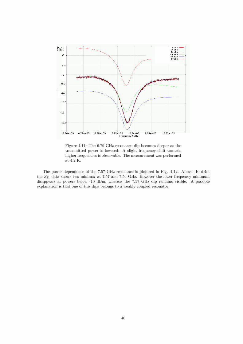
Figure 4.11: The 6.79 GHz resonance dip becomes deeper as thetransmitted power is lowered. A slight frequency shift towardshigher frequencies is observable. The measurement was performedat 4.2 K.
The power dependence of the 7.57 GHz resonance is pictured in Fig. 4.12. Above -10 dBmthe S21 data shows two minima: at 7.57 and 7.56 GHz. However the lower frequency minimumdisappears at powers below -10 dBm, whereas the 7.57 GHz dip remains visible. A possibleexplanation is that one of this dips belongs to a weakly coupled resonator.
40

Figure 4.12: At high powers the resonance at 7.57 GHz shows twominima, however at lower powers the lower minimum disappears,while the upper minimum becomes more distinct. The measure-ment was performed at 4.2 K.
In case of the 7.86 GHz resonance we again see the dip becoming more distinct as the trans-mitted power is decreased (Fig. 4.13). Here the effect is even more striking as in case of the 6.79GHz resonance.
41

Figure 4.13: Lowering the transmitted power, we observe that the7.86 GHz resonance dip becomes more distinct. The measurementwas performed at 4.2 K.
4.2.4 Temperature Dependence of the Frequency and the Quality Fac-
tors of the 6.79 GHz Resonance
Lowering the vapour pressure inside the helium Dewar temperatures down to 3.2 K - correspondinga vapour pressure of 300 mbar - were achieved. As the temperature was decreasing, the dips becamedeeper and internal quality factors higher, also the frequencies shifted to higher values. Table 4.4shows the temperature dependence of frequency and quality factor of the 6.79 GHz resonance.
Vapour pressure Temperature / K Frequency / GHz Qi / 103 QC / 103 Error of Fit
1000 mbar 4.2 6.79 0.80 3.9 2.3 · 10−5
700 mbar 3.9 6.82 1.1 3.7 1.1 · 10−4
300 mbar 3.2 6.84 3.4 1.7 4.5 · 10−3
Table 4.4: Temperature dependence of internal and coupling qual-ity factors of the 6.79 resonance dip. Resonance frequency shiftswith temperature. For dependence of temperature upon vapourpressure see Ref. [22].
42

Conclusion
This thesis shows how the task of designing superconducting microwave spiral resonators was ap-proached by means of electromagnetic simulation (using Sonnet) of created layouts (LEdit). Thedesigned resonators were measured and found to be functional, having resonance frequencies inthe range expected from simulations. The work also provides an overview of the basic propertiesof superconductors and of lumped element resonator theory. A lumped elements model was intro-duced to describe qualitatively the scattering parameters of a spiral resonator capacitively coupledto a feedline and to understand the behavior of its quality factor.
43

Acknowledgement
I want to thank Prof. Dr. Alexey Ustinov for giving me the opportunity to work in his groupand Dr. Martin Weides for his most patient and throughout helpful, constructive supervision. Iam also grateful to Tobias Bier for fabricating the measured resonators and I thank Philipp Jungfor helping me with IT problems at the beginning of my work, as I do thank all members of theUstinov group for the help I received.
44

Bibliography
[1] G. V. Eleftheriades and K. G. Balmain. Negative-refraction metamaterials: fundamental
principles and applications. John Wiley & Sons, 2005.
[2] V. G. Veselago. The electrodynamics of substances with simultaneously negative values of ǫand µ. Physics-Uspekhi, 10(4):509–514, 1968.
[3] C. Kurter, A. P. Zhuravel, J. Abrahams, C. L. Bennett, A. V. Ustinov, and S. M. Anlage.Superconducting rf metamaterials made with magnetically active planar spirals. Applied
Superconductivity, IEEE Transactions on, 21(3):709–712, 2011.
[4] B. Ghamsari, J. Abrahams, S. Remillard, and S. Anlage. High-temperature superconductingspiral resonators for metamaterials applications. Applied Superconductivity, IEEE Transac-
tions on, 23(3), 2012.
[5] H. Kamerlingh Onnes. The superconductivity of mercury. Comm. Phys. Lab. Univ. Leiden,122:124, 1911.
[6] C. Kittel. Einfuhrung in die Festkorperphysik. Oldenbourg, 15th edition, 2013.
[7] G. Muenster. Quantentheorie. De Gruyter, 2nd edition, 2010.
[8] M. Neuwirth. Investigation of field distribution in superconducting microwave resonators.Bachelor thesis, Karlsruhe Institute of Technology, 2013.
[9] S. Hunklinger. Festkorperphysik. Oldenbourg, 3rd edition, 2011.
[10] M. Tinkham. Introduction to Superconductivity. Dover Publications, second edition, 2004.
[11] B. S. Deaver and W. M. Fairbank. Experimental evidence for quantized flux in supercon-ducting cyclinders. Physical Review Letters, 7(2):43–46, 1961.
[12] E. Babaev, J. Carlstrom, J. Garaud, M. Silaev, and J. M. Speight. Type-1.5 superconductivityin multiband systems: Magnetic response, broken symmetries and microscopic theory–a briefoverview. Physica C: Superconductivity, 479:2–14, 2012.
[13] W. Buckel and R. Kleiner. Superconductivity. Wiley-VCH, second edition, 2004.
[14] W. Greiner. Klassische Elektrodynamik. Harri Deutsch Verlag, 6th edition, 2002.
[15] D. M. Pozar. Microwave Engineering. Wiley, 3rd edition edition, 2005.
[16] M. Goppl, A. Fragner, M. Baur, R. Bianchetti, S. Filipp, J. M. Fink, P. J. Leek, G. Puebla,L. Steffen, and A. Wallraff. Coplanar waveguide resonators for circuit quantum electrody-namics. Journal of Applied Physics, 104(11):113904–113904, 2008.
[17] D. Wisbey, A. Reinisch, W. Gardner, J. Brewster, and J. Gao. New method for determiningthe quality factor and resonance frequency of superconducting micro-resonators from sonnetsimulation. Bulletin of the American Physical Society, 58(1), 2013.
45

[18] http://www.tannereda.com/products/l-edit pro.
[19] D. Bothner, T. Gaber, M. Kemmler, D. Koelle, and R. Kleiner. Improving the perfor-mance of superconducting microwave resonators in magnetic fields. Applied Physics Letters,98(10):102504–102504, 2011.
[20] http://www.sonnetsoftware.com/about/.
[21] J. Gao. The Physics of Superconducting Microwave Resonators. PhD thesis, CaliforniaInstitute of Technology, 2008.
[22] Ch. Enss and S. Hunklinger. Tieftemperaturphysik. Springer, 2000.
46