design and implementation of efficient curve tracer for ... · pdf fileinternational journal...
TRANSCRIPT

International Journal on Electrical Engineering and Informatics - Volume 7, Number 1, March 2015
Design and Implementation of Efficient Curve Tracer for Photovoltaic System under Partial Shaded Conditions
R. Ramaprabha, S. H. Jubair, K. Suhas, and A. Lokesh
Department of EEE, SSN College of Engineering, Chennai, Tamilnadu, India
[email protected], [email protected], [email protected], [email protected]
Abstract: Photovoltaic (PV) panels are subjected to problems such as hot spots and reduced output power when operating in partially shaded conditions. Although bypass diodes are utilized to alleviate these problems, the diodes cause multiple-peak characteristics. Tracking the maximum output power in partially shaded conditions is difficult using conventional software-based maximum power point tracking (MPPT) techniques. Curve tracers can assist software-based MPPT to track the true/global maximum power point (MPP) by scanning several potential MPP areas. Therefore, a software-based MPPT with an I-V curve tracer is a preferred solution. Moreover, curve tracers reveal more about the PV array performance and the fastest method to do so. This paper investigates the advantages and disadvantages of several I-V curve tracers and proposes a load self-adaptive PV panel characteristic curve tracer by applying a hysteretic self-controlled duty-modulated load resistor (DMLR) to a boost converter I-V curve tracer. Several advantages are achieved such as simple structure, cost-efficient implementation and no tracing limitation near the Voc. A circuit for 72 W PV panel is used to verify the feasibility of the proposed curve tracer. Keywords: Photovoltaic system, Boost Converter, Duty Modulated Load Resistor (DMLR), Curve tracer, PSpice. 1. Introduction Awareness of the global warming and continuous increase in global electricity energy consumption has drawn attention towards the renewable energy sources. Among the renewable energy sources, power generation from solar photovoltaic (PV) system becomes more popular, because it is a clean energy source and abundant in nature. Photovoltaic panels generate direct electricity. The main problem in PV system is its non-linear characteristics which make the extraction of maximum power a difficult task. The tracking of MPP becomes more difficult because of the usage of bypass diodes in case of partially shaded PV array. PV panels are subject to problems such as hot spots and reduced output power when operating in partially shaded conditions. Bypass diodes are utilized to overcome these problems [1]-[6], but they introduce multiple peaks in the characteristics [7]-[8]. In this case, tracking of MPP is difficult using conventional software-based maximum power point tracking (MPPT) techniques [9]-[15]. Current-voltage (I-V) curve tracers can assist software-based MPPT to track the true maximum power point (MPP) by scanning several potential MPP areas. Therefore, software-based MPPT with an I-V curve tracer is a preferred solution. Among several I-V curve tracers, boost converter I-V curve tracer has many advantages, which include simple circuit, low implementation cost and continuous input current. However, conventional boost converter I-V curve tracers have a tracing limitation near Voc area [15]. To solve this problem, a load self-adaptive PV panel characteristic curve tracer is proposed by applying a hysteretic self-controlled duty-modulated load resistor (DMLR) to a boost curve tracer, called an improved boost converter I-V curve tracer [14]. In this paper, the detailed design of PV fed improved boost converter based I-V curve tracer has been discussed. The analysis has been carried out using PSpice software [16] with 72 WP
Received: October 5th, 2014. Accepted: March 26th, 2015 DOI: 10.15676/ijeei.2015.7.1.11
140

array. The designed circuit has been validated through hardware implementation with proposed curve tracer and the results are presented. 2. System Description The schematic diagram of the proposed system is shown in Figure 1.
Figure 1. Schematic of the proposed system
The components of the system include a 72 WP PV array (two 36 WP panels in series), a boost converter, duty modulated load resistor (DMLR) and pulse generating circuit. A detailed design, modelling and simulation of each section in the schematic are discussed in the following sections. A. Modelling and Simulation of PV System using PSpice In this paper, SOLKAR make PV panel is considered. Each panel consists of 36 cells in series and the technical specifications of a single panel at standard test condition (STC: G= 1000 W/m2, T=25oC, AM =1.5 m/s) are given as; Short circuit current, Isc = 2.55 A, Open circuit voltage, Voc = 21.24 V, Maximum Power, Pmax = 37.08 W, Maximum power point voltage, Vmax = 16.54 V and Maximum power point current, Imax = 2.25 A. The modeling and simulation of PV panel have been carried out using PSpice software by considering one diode model of PV [15]. The parameters like shunt resistance, series resistance, diode saturation current and diode ideality factor are suitably modified to get the required characteristics. The simulation model has been validated against the panel characteristics at important points like Isc, Voc, Vmax, Imax and Pmax. The simulated I-V and P-V characteristics at STC are shown in Figure 2 indicating the knee points.
Figure 2. Characteristics of PV panel obtained using PSpice
R. Ramaprabha, et al.
141
B. Design and Simulation of an Improved Boost converter In order to show the effectiveness of the proposed curve tracer, a small array (72 W) of two series connected panel is considered in this work. The proposed curve tracer has two parts as shown in Figure 1. The first part is boost converter with closed loop control circuit and the other part is DMLR stage containing a duty-modulated load resistor with hysteretic self-controlled circuit. The boost converter stage is same as a conventional boost V-I curve tracer where the converter pushes a panel operating point to a load operating point which has same power level. In the proposed system, a closed loop circuit forces the converter to operate at any particular operating point voltage (Vop) by using a proper reference voltage (Vref). This loop makes the boost curve tracer more stable and controllable. As a result, accurate and flexible I-V curve tracing is achieved. The duty cycle of Q1 is controlled by a reference signal Vref with negative feedback. When the sense voltage, Vsen is higher than the reference voltage Vref, the duty cycle of Q1 will increase. A larger duty cycle increases the operating current of the PV panel. In the meantime, Vsen will reduce to trace Vref. To ensure the system stability Rcomp and Ccomp are added. The values of sensing resistors R1 and R2 are calculated as in (1).
maxref,VsenV2R1R
2RocV ≤=+× (1)
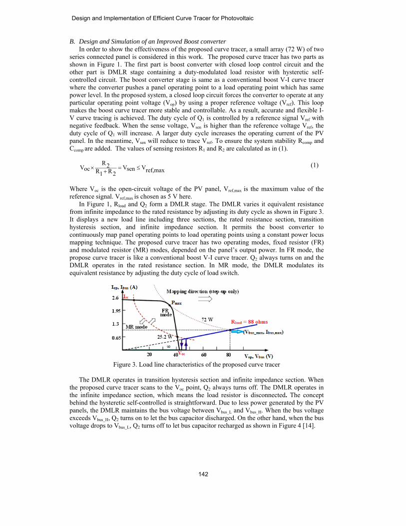
Where Voc is the open-circuit voltage of the PV panel, Vref,max is the maximum value of the reference signal. Vref,max is chosen as 5 V here. In Figure 1, Rload and Q2 form a DMLR stage. The DMLR varies it equivalent resistance from infinite impedance to the rated resistance by adjusting its duty cycle as shown in Figure 3. It displays a new load line including three sections, the rated resistance section, transition hysteresis section, and infinite impedance section. It permits the boost converter to continuously map panel operating points to load operating points using a constant power locus mapping technique. The proposed curve tracer has two operating modes, fixed resistor (FR) and modulated resistor (MR) modes, depended on the panel’s output power. In FR mode, the propose curve tracer is like a conventional boost V-I curve tracer. Q2 always turns on and the DMLR operates in the rated resistance section. In MR mode, the DMLR modulates its equivalent resistance by adjusting the duty cycle of load switch.
Figure 3. Load line characteristics of the proposed curve tracer
The DMLR operates in transition hysteresis section and infinite impedance section. When the proposed curve tracer scans to the Voc point, Q2 always turns off. The DMLR operates in the infinite impedance section, which means the load resistor is disconnected. The concept behind the hysteretic self-controlled is straightforward. Due to less power generated by the PV panels, the DMLR maintains the bus voltage between Vbus_L and Vbus_H. When the bus voltage exceeds Vbus_H, Q2 turns on to let the bus capacitor discharged. On the other hand, when the bus voltage drops to Vbus_L, Q2 turns off to let bus capacitor recharged as shown in Figure 4 [14].
Design and Implementation of Efficient Curve Tracer for Photovoltaic
142
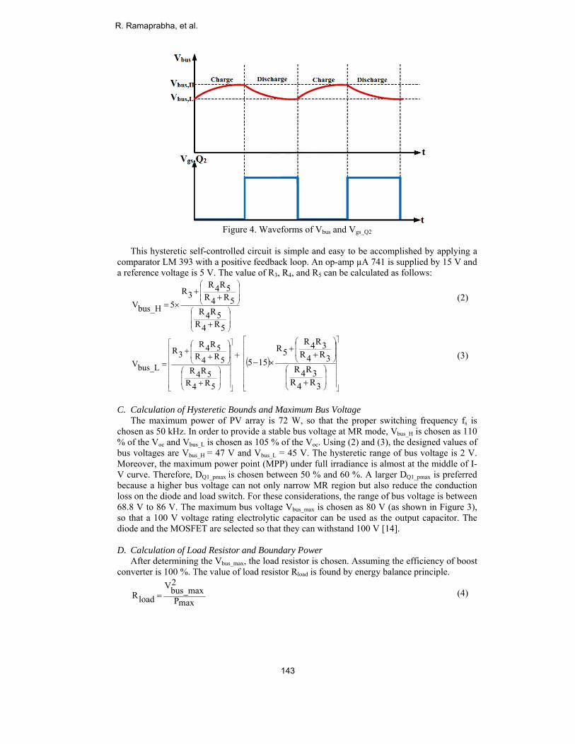
Figure 4. Waveforms of Vbus and Vgs_Q2
This hysteretic self-controlled circuit is simple and easy to be accomplished by applying a comparator LM 393 with a positive feedback loop. An op-amp µA 741 is supplied by 15 V and a reference voltage is 5 V. The value of R3, R4, and R5 can be calculated as follows:
⎟⎟⎟
⎠
⎞
⎜⎜⎜
⎝
⎛
⎟⎟⎟
⎠
⎞
⎜⎜⎜
⎝
⎛
+
++
×=
5R4R5R4R
5R4R5R4R
3R5bus_HV
(2)
⎥⎥⎥⎥⎥⎥⎥
⎦
⎤
⎢⎢⎢⎢⎢⎢⎢
⎣
⎡
⎟⎟
⎠
⎞
⎜⎜
⎝
⎛
⎟⎟
⎠
⎞
⎜⎜
⎝
⎛
+
++
=
5R4R5R4R
5R4R5R4R
3R
bus_LV+ ( )
⎥⎥⎥⎥⎥⎥⎥
⎦
⎤
⎢⎢⎢⎢⎢⎢⎢
⎣
⎡
⎟⎟
⎠
⎞
⎜⎜
⎝
⎛
⎟⎟
⎠
⎞
⎜⎜
⎝
⎛
+
++
×−
3R4R3R4R
3R4R3R4R
5R155
(3)
C. Calculation of Hysteretic Bounds and Maximum Bus Voltage The maximum power of PV array is 72 W, so that the proper switching frequency fs is chosen as 50 kHz. In order to provide a stable bus voltage at MR mode, Vbus_H is chosen as 110 % of the Voc and Vbus_L is chosen as 105 % of the Voc. Using (2) and (3), the designed values of bus voltages are Vbus_H = 47 V and Vbus_L = 45 V. The hysteretic range of bus voltage is 2 V. Moreover, the maximum power point (MPP) under full irradiance is almost at the middle of I-V curve. Therefore, DQ1_pmax is chosen between 50 % and 60 %. A larger DQ1_pmax is preferred because a higher bus voltage can not only narrow MR region but also reduce the conduction loss on the diode and load switch. For these considerations, the range of bus voltage is between 68.8 V to 86 V. The maximum bus voltage Vbus_max is chosen as 80 V (as shown in Figure 3), so that a 100 V voltage rating electrolytic capacitor can be used as the output capacitor. The diode and the MOSFET are selected so that they can withstand 100 V [14]. D. Calculation of Load Resistor and Boundary Power After determining the Vbus_max, the load resistor is chosen. Assuming the efficiency of boost converter is 100 %. The value of load resistor Rload is found by energy balance principle.
maxP
2bus_maxV
loadR = (4)
R. Ramaprabha, et al.
143

Where Vbus_max is 80 V, Pmax is 72 W, and Rload is 88 Ω. The maximum power dissipation of load resistor is chosen as 90 W with 20 % de-rating. After Rload is chosen, Pboundary between FR mode and MR mode is calculated as follows.
loadR
2bus_HV
boundaryP = (5)
Pboundary is 25.2 W (35 % of Pmax). When the PV power exceeds 35 % of Pmax, the improved boost converter based I-V curve tracer operates in FR mode. Otherwise, it operates in MR mode. Under full irradiance, the operating voltage at MPP (Vmax) is referred from the specification. The input inductor is assumed to be large enough. The duty cycle of Q1 can be found by the voltage gain equation of boost converter under continuous conducted mode (CCM) as follows:
bus_maxV
maxVbus_maxVQ1_PmaxD
−= (6)
Where Vbus_max is 80 V, Vmax is 34.4 V and DQ1_pmax is 56.8 %. After calculating DQ1_pmax, the inductor is designed with a proper input current ripple at MPP Δ IL_pmax by using (7).
sfL_pmaxΔI
Q1_maxDpmaxVL
×
×= (7)
Where Δ IL_pmax is chosen as 28 % of the operating current at MPP (Ipmax). The inductance is designed 3 mH using (7). Although boost converter provides a continuous input current, there is still a small current ripple. Therefore, an input capacitor acting as an input filter is necessary. It improves the high frequency switching noise which may affect the I-V curve measurement. A larger capacitor leads a small input voltage ripple. However, it may also cause longer response time, extra cost and layout space. Filter capacitor Cin is calculated as,
sfin_pmaxΔV8L_pmaxΔI
inC××
= (8)
Where ΔVin_pmax is the input voltage ripple at MPP, Δ Vin_pmax is chosen as 0.15 % of Vpmax, and the input capacitor Cin is calculated as 150 μF. Cout needs to meet the bus voltage ripple Δ Vbus_pmax at MPP. The output capacitor is designed by (9).
sfbus_pmaxΔV
Q1_pmaxDbus_maxIoutC
×
×= (9)
Where DQ1_pmax is 56.8%, fs is 50 kHz, Δ Vbus_pmax is chosen as 1 % of Vbus_max and Cout is 64 μF. MOSFET and diode are selected with proper current and voltage ratings. When the improved boost converter V-I curve tracer traces Isc point, the duty of Q1 is equal to 100%. Therefore, the maximum current flowing through boost switch Q1 is Isc. When operating at MPP, Vds_max of Q1 is Vbus_max. As a result, Q1 is chosen as 100V/5A MOSFET. For the diode, when operating at MPP, peak inverse voltage (PIV) of boost diode and the Vds_max of load switch are Vbus_max. Also, for both of D and Q2, the maximum current flowing through them is the maximum bus current Ibus_max [14].
Design and Implementation of Efficient Curve Tracer for Photovoltaic
144

loadRbus_maxV
bus_maxI = (10)
Ibus_max is 1.5 A, diode is chosen as 100V/3A Schottky diode and load switch Q2 is chosen as 100V/3A MOSFET. 3. Simulation results and Inference The proposed curve tracer is simulated to prove its feasibility by PSpice software. In this section, I-V curve and P-V curve are measured not only under uniform irradiance but also under partial shading. Case 1: Uniform insolation condition The two PV panels are operating under full irradiance level, Isc1 = Isc2 = 2.55 A. The characteristics curves are shown in Figure 5. The maximum power (Pmax= 74.26 W) occurs when Vop= 34.04 V.
Figure 5. Characteristics of PV array under uniform insolation conditions (Isc1=Isc2=2.55 A)
Case 2: Non-uniform insolation condition 1 When PV panel operates under partial shading, Isc value is reduced. Under different shaded levels, the global MPP may occur at higher or lower voltage as mentioned earlier. P-V curve has a global MPP at a lower voltage when Isc2 < 0.5 Isc1. A condition, Isc1 = 2 A and Isc2 = 0.7 A, is an example. The characteristics of this condition are shown in Figure 6. The global MPP of Pmax = 26.41 W occurs at the lower voltage (Vop =16.25 V).
Figure 6. Characteristics of PV array under partial shaded conditions (Isc1=2A & Isc2=0.7A)
Case 3: Non-uniform insolation condition 2 On the contrary, the global MPP occurs at higher voltage when Isc2 > 0.5 Isc1. Under a condition, Isc1 = 2.55 A and Isc2 = 1.55 A, the characteristics are shown in Fig 7. The global MPP (Pmax = 46.55 W) occurs at higher voltage (Vop = 34.86 V).
R. Ramaprabha, et al.
145

Figure 7. Characteristics of PV array under partial shaded conditions (Isc1=2.55 A & Isc2 =1.55
A) For different shading conditions, the developed tracing system is validated and results are consolidated in Table 1.
Table 1. Simulation Parameters
Insolation levels (W/m2)
Panel Currents (A) Array Parameters
Isc1 (A) Isc2 (A) Voc (V) Isc (A) Vmax (V) Imax
(A) Pmax (W)
1000,1000 2.55 2.55 43.10 2.54 34.04 2.19 74.26 1000, 608 2.55 1.55 41.49 2.53 34.86 1.33 46.55 800, 275 2 0.7 40.20 1.98 16.25 1.62 26.41
4. Hardware Implementation The proposed curve tracer shown in Figure1 is implemented in hardware with designed values. In this work two series connected panels are used for testing. One of the solar panels is kept under full illumination whereas another is subjected to partially shaded conditions, using artificial light source, as shown in Figure 8. In case of partially illuminated panel, the insolation level received by the module has been changed using tilting stand arrangement. The improved boost converter is realized with proper component selection as discussed in Section 2. The switch used is IRFP460 (Metal Oxide Semiconductor Field Effect Transistor) which is TO-247 package type. It is an N-channel MOSFET and its rating is 500V and 20A. The diode used id IN5408 with the current rating of 3A. The inductor (3mH) is designed by winding appropriate turns of insulated copper coil on an E core. The hysteretic self-controlled DMLR circuit is simple and easy to be accomplished by applying a comparator µA741 with a positive feedback loop. µA741 is supplied by 15 V and a reference voltage is 5 V. The complete system is fed by the small PV array. The hardware setup of the power circuit is shown in the Figure 8.
Figure 8. Hardware setup of the proposed curve tracer system
Vop and Iop of a PV panel are traced under partial shaded condition as shown in Figure 9.a. The oscilloscope is switched to X-Y mode to trace I-V curve, and is shown in Figure 9.b.
Design and Implementation of Efficient Curve Tracer for Photovoltaic
146
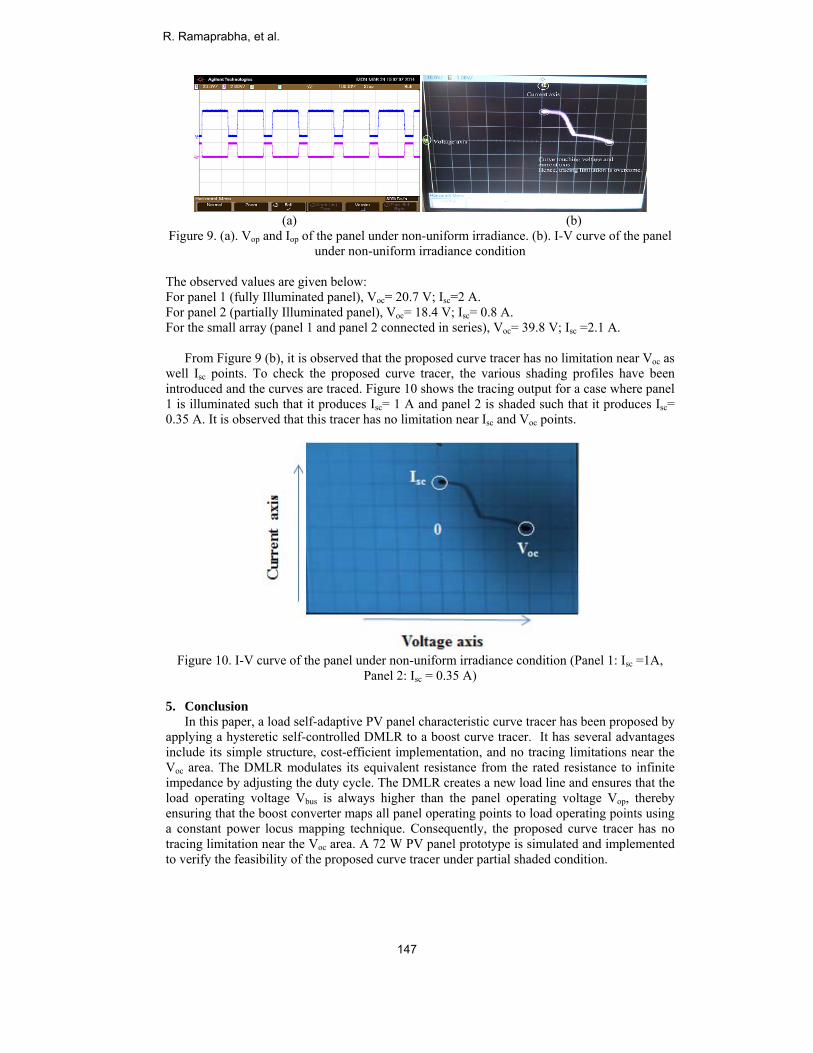
(a) (b) Figure 9. (a). Vop and Iop of the panel under non-uniform irradiance. (b). I-V curve of the panel
under non-uniform irradiance condition
The observed values are given below: For panel 1 (fully Illuminated panel), Voc= 20.7 V; Isc=2 A. For panel 2 (partially Illuminated panel), Voc= 18.4 V; Isc= 0.8 A. For the small array (panel 1 and panel 2 connected in series), Voc= 39.8 V; Isc =2.1 A. From Figure 9 (b), it is observed that the proposed curve tracer has no limitation near Voc as well Isc points. To check the proposed curve tracer, the various shading profiles have been introduced and the curves are traced. Figure 10 shows the tracing output for a case where panel 1 is illuminated such that it produces Isc= 1 A and panel 2 is shaded such that it produces Isc= 0.35 A. It is observed that this tracer has no limitation near Isc and Voc points.
Figure 10. I-V curve of the panel under non-uniform irradiance condition (Panel 1: Isc =1A,
Panel 2: Isc = 0.35 A)
5. Conclusion In this paper, a load self-adaptive PV panel characteristic curve tracer has been proposed by applying a hysteretic self-controlled DMLR to a boost curve tracer. It has several advantages include its simple structure, cost-efficient implementation, and no tracing limitations near the Voc area. The DMLR modulates its equivalent resistance from the rated resistance to infinite impedance by adjusting the duty cycle. The DMLR creates a new load line and ensures that the load operating voltage Vbus is always higher than the panel operating voltage Vop, thereby ensuring that the boost converter maps all panel operating points to load operating points using a constant power locus mapping technique. Consequently, the proposed curve tracer has no tracing limitation near the Voc area. A 72 W PV panel prototype is simulated and implemented to verify the feasibility of the proposed curve tracer under partial shaded condition.
R. Ramaprabha, et al.
147

6. Acknowledgement The authors wish to thank the management of SSN College of Engineering, Chennai for providing internal funding to carry out this work. 7. References [1] P. Abete, C. Cane, M. Rizzitano, Tarantino and R. Tomasini, “Performance testing
procedures for photovoltaic panels in mismatching conditions”, Proceedings of IEEE PVSC, pp. 807-811, 1991.
[2] J. W. Bishop, “Computer simulation of the effect of electrical mismatches in photovoltaic interconnection circuits”, Solar Cells, Vol. 25, No. 1, pp. 73-89, June 1988.
[3] W. Herrmann, W. Wiesner, and W. Vaassen, “Hot spot investigations on PV panels - new concepts for a test standard and consequences for panel design with respect to bypass diodes”, Proceedings of IEEE PVSC, pp. 1129-1132, 1997.
[4] J. W. Bishop, “Micro-plasma breakdown and hot-spots in silicon solar cells”, Solar Cells, Vol. 26, No. 4, pp. 335-349, Sept. 1989.
[5] V. Quaschning, “Numerical simulation of current voltage characteristics of photovoltaic systems with shaded solar cells,” Solar Energy, Vol. 56, No. 6, pp. 513-520, June 1996.
[6] E. Molenbroek, D. W. Waddington and K. A. Emmery, “Hot spot susceptibility and testing of PV panels”, Proceedings of IEEE PVSC, pp. 547-552, 1991.
[7] R. Ramaprabha and B. L. Mathur, “MATLAB based modelling to study the influence of shading on series connected SPVA”, Proceedings of ICETET, pp. 30-34, 2009.
[8] Atsushi Kajihara and Tetsumi Harakawa, “Model of photovoltaic cell circuits under partial shading”, Proceedings of IEEE ICIT, pp. 866-870, 2005.
[9] K. Kobayashi, I. Takano, and Y. Sawada, “A study on a two stage maximum power point tracing control of a photovoltaic system under partial shaded isolation conditions,” in Proceedings of IEEE PES, 2003, pp. 2612-2617.
[10] Peng Lei, Yaoyu Li, and John E. Seem, “Sequential ESC-based global MPPT control for photovoltaic array with variable shading”, IEEE Transactions on Sustainable Energy, Vol. 2, No. 3, pp. 348-358, July 2011.
[11] Tat Luat Nguyen and Kay-Soon Low, “A global maximum power tracing scheme employing DIRECT search algorithm for photovoltaic systems,” IEEE Transactions on Industrial Electronics, Vol. 57, No. 10, pp. 3456-3467, Oct. 2010.
[12] R. Alonso, P. Ibaez, V. Martinez, E. Roman and A. Sanz, “An innovative perturb, observe and check algorithm for partially shaded PV systems”, Proceedings of IEEE European Conference on Power Electronics and Applications, pp. 1-8, 2009.
[13] Hiren Patel and Vivek Agarwal, “Maximum power point tracing scheme for PV system operating under partially shaded conditions”, IEEE Transactions on Industrial Electronics, Vol. 55, No. 4, pp. 1689-1698, April 2008.
[14] R. Ramaprabha, S. H. Jubair,K. Suhas and A. Lokesh, “ Development of Improved Curve Tracer forPhotovoltaic System under Partial Shaded Conditions”, Proceedings of 2014 International Conference on Circuit, Power and Computing Technologies (ICCPCT), 2014.
[15] Yan Chun Yi and Lv Jinshan, “Load adaptive characteristic curves scanner solar panels”, ROC hundred and July 20, 2001.
[16] www.cadence.com
Design and Implementation of Efficient Curve Tracer for Photovoltaic
148

and memtechnique
R. RChenfromPhD been paperconfephoto
mber in IEEE. es for renewabl
S. HEngicomphe isSolut
K. SEngicomphe is
A. LoEngincompis woBhad
Ramaprabha isnnai, Tamilnad
m Bharathidasandegree from Aworking in th
rs in Nationerences and 5ovoltaic and poHer areas of
le energy sourc
H. Jubair was ineering, SSN pleted this pros working as ations, Chennai
Suhas was anineering, SSN pleted this pros doing Master
okesh was an uneering, SSN Cpleted this projeorking as an Eledrachalam, AP,
s an Associate du, India since n University inAnna Universite teaching fielal conference
50 papers in iower electroni
f interest incluces.
an undergradCollege of Eng
oject under SSNan Associate Soi, India.
n undergraduaCollege of En
oject under SSs in EE at Texa
undergraduate College of Engect under SSN ectrical Manag India.
Professor in S2001. She obt
n 1997 and 200ty in the area old for about 14es, 62 papersinternational jics & drives. Sude Solar PV
duate student ogineering, CheN Student Inteoftware Engin
ate student ofgineering, Che
SN Student Intas Tech Univer
student of Elecineering, ChenStudent Intern
ger(Operations)
SSN College otained B.E and00 respectivelyof solar PV sys4 years. She has in referredournal in the
She is a life meSystems, Pow
of Electrical anennai, TamilNaernally funded
neer at Wolters
f Electrical anennai, TamilNaernally fundedrsity
ctrical and Elecnnai, TamilNadnally funded pr) at ITC PSPD
of Engineering,d M.E. degreesy. She obtainedstems. She has
as published 27d International
area of solarember in ISTE
wer conversion
nd Electronicsadu, India. Hed project. Nows Kluwer-ELM
nd Electronicsadu, India. Hed project. Now
ctronics du, India. He roject. Now he
, s d s 7 l r
E n
s e
w M
s e
w
R. Ramaprabha, et al.
149