design and analysis of electromagnetic interference
TRANSCRIPT

Clemson UniversityTigerPrints
All Dissertations Dissertations
5-2014
Design and Analysis of ElectromagneticInterference Filters and ShieldsAndrew McDowellClemson University, [email protected]
Follow this and additional works at: https://tigerprints.clemson.edu/all_dissertations
Part of the Electrical and Computer Engineering Commons
This Dissertation is brought to you for free and open access by the Dissertations at TigerPrints. It has been accepted for inclusion in All Dissertations byan authorized administrator of TigerPrints. For more information, please contact [email protected].
Recommended CitationMcDowell, Andrew, "Design and Analysis of Electromagnetic Interference Filters and Shields" (2014). All Dissertations. 1368.https://tigerprints.clemson.edu/all_dissertations/1368

DESIGN AND ANALYSIS OF ELECTROMAGNETIC INTERFERENCE FILTERS AND SHIELDS
A Dissertation Presented to
the Graduate School of Clemson University
In Partial Fulfillment of the Requirements for the Degree
Doctor of Philosophy Electrical Engineering
by Andrew Joel McDowell
May 2014
Accepted by: Todd H. Hubing, Committee Chair
Anthony Q. Martin Pingshan Wang Simona Onori

ii
ABSTRACT
Electromagnetic interference (EMI) is a problem of rising prevalence as electronic
devices become increasingly ubiquitous. EMI filters are low pass filters intended to
prevent the conducted electric currents and radiated electromagnetic fields of a device
from interfering with the proper operation of other devices. Shielding is a method, often
complementary to filtering, that typically involves enclosing a device in a conducting box
in order to prevent radiated EMI. This dissertation includes three chapters related to the
use of filtering and shielding for preventing electromagnetic interference.
The first chapter deals with improving the high frequency EMI filtering
performance of surface mount capacitors on printed circuit boards (PCBs). At high
frequencies, the impedance of a capacitor is dominated by a parasitic inductance, thus
leading to poor high frequency filtering performance. Other researchers have introduced
the concept of parasitic inductance cancellation and have applied this concept to
improving the filtering performance of volumetrically large capacitors at frequencies up
to 100 MHz. The work in this chapter applies the concept of parasitic inductance
cancellation to much smaller surface mount capacitors at frequencies up to several
gigahertz.
The second chapter introduces a much more compact design for applying parasitic
inductance cancellation to surface mount capacitors that uses inductive coupling between
via pairs as well as coplanar traces. This new design is suited for PCBs having three or
more layers including solid ground and/or power plane(s). This design is demonstrated to

iii
be considerably more effective in filtering high frequency noise due to crosstalk than a
comparable conventional shunt capacitor filter configuration.
Finally, chapter 3 presents a detailed analysis of the methods that are used to
decompose the measure of plane wave shielding effectiveness into measures of
absorption and reflection. Textbooks on electromagnetic compatibility commonly
decompose shielding effectiveness into what is called the Schelkunoff decomposition in
this work with terms called penetration loss, reflection loss, and the internal reflections
correction term. In experimentally characterizing the shielding properties of materials,
however, other decompositions are commonly used. This chapter analyzes the
relationships between these different decompositions and two-port network parameters
and shows that other decompositions offer terms that are better figures of merit than the
terms of the Schelkunoff decomposition in experimental situations.

iv
ACKNOWLEDGMENTS
I would especially like to thank my advisor, Dr. Todd H. Hubing for his guidance
and support throughout my graduate school career. Dr. Hubing’s enthusiasm for
electromagnetic compatibility research is truly inspiring. It has been a pleasure to work
with him.
I would also like to thank the other members of my PhD advisory committee: Dr.
Anthony Q. Martin, Dr. Pingshan Wang, and Dr. Simona Onori for their helpful
comments. I would also like to acknowledge the help that I have received from my
graduate student colleagues at Clemson at various times.
Finally, I also appreciate how supportive my parents and brothers have been of
me. My parents have come out to visit me quite a bit and they always want to hear about
my work.

v
TABLE OF CONTENTS
Page
ABSTRACT ..................................................................................................................... ii
ACKNOWLEDGMENTS .............................................................................................. iv
LIST OF TABLES ......................................................................................................... vii
LIST OF FIGURES ...................................................................................................... viii
CHAPTER
1 Parasitic Inductance Cancellation for Surface Mount Shunt Capacitor Filters ..................................................................................................... 1
Abstract .................................................................................................................. 1
1.1 Introduction ................................................................................................... 1
1.2 Theory and Characterization of Parasitic Inductance ................................... 4
1.2.1 Review of Capacitor Parasitics ......................................................... 4
1.2.2 Cancellation of Parasitic Inductance ................................................ 7
1.3 Designs Optimized and Compared ............................................................... 9
1.4 Simulation of Parameterized Designs ......................................................... 10
1.5 Construction and Measurement of Designs ................................................ 17
1.5.1 Comparison of “Best” Cancellation Coil Between Different Designs ............................................................. 21
1.5.2 Comparison with Controls and Other Methods for Improving High Frequency Attenuation ................................... 23
1.6 Analysis of Cancellation Scheme ............................................................... 26
1.6.1 Determining Values of Secondary Parasitic Lumped Components ...................................................................... 27
1.6.2 Lumped Model Simulations of Designs ......................................... 29
1.7 Conclusion .................................................................................................. 32
References ............................................................................................................ 32
2 A Compact Implementation of Parasitic Inductance Cancellation for Shunt Capacitor Filters on Multilayer PCBs ............................. 35
Abstract ................................................................................................................ 35
2.1 Introduction ................................................................................................. 35
2.2 Proposed Design and Rationale .................................................................. 37
2.3 Design Procedure ........................................................................................ 39 2.3.1 Validation of Capacitor Model ....................................................... 41
2.4 Implementation on a Three Layer PCB ...................................................... 43
2.5 Implementation on a Four-Layer PCB ....................................................... 47

vi
Table of Contents (Continued)
Page
2.6 Example Application to I/O Filtering ......................................................... 49
2.7 Conclusion .................................................................................................. 54
References ............................................................................................................ 54
3 Decomposition of Shielding Effectiveness into Absorption and Reflection Components ................................................................................. 57
Abstract ................................................................................................................ 57
3.1 Introduction ................................................................................................. 58
3.2 Review of Transmission Line Model of Shielding ..................................... 62
3.3 Schelkunoff Decomposition of Shielding Effectiveness ............................ 66
3.3.1 Determining Decomposition from Scattering Parameters ....................................................................................... 68
3.3.2 Determining Power Distribution from Decomposition ................................................................................ 69
3.3.3 Application to Layered Shields ...................................................... 72
3.4 Mismatch Decomposition ........................................................................... 75
3.4.1 Basic Description ............................................................................ 75
3.4.2 Comparison to Schelkunoff Decomposition ................................... 77
3.5 Examples ..................................................................................................... 79
3.6 Conclusion .................................................................................................. 83
Appendix: Image Parameters and Schelkunoff Decomposition .......................... 85
References ............................................................................................................ 88

vii
LIST OF TABLES
Table Page
Table 1.1. Comparison of Parameters Including Experimentally Optimized Parameter for Different Designs ............................................... 23
Table 1.2. Parasitic Capacitances Measured with Network Analyzer and Lumped Model Inductances Calculated with FASTHENRY ..................................................................................... 29
Table 2.1. Comparison of Measured and Simulated Parasitic Inductances of Conventional Shunt Capacitor Filters ................................ 42
Table 2.2. Summary of Different Boards Tested and Letter Codes Assigned to Each ........................................................................................ 51

viii
LIST OF FIGURES
Figure Page
Fig. 1.1. (a) Example schematic of an ideal shunt capacitor filter. (b) Example schematic of shunt capacitor filter with parasitics. (c) Calculated insertion gain for these two filters. ..................................................................................................... 5
Fig. 1.2. (a) Transformer T-equivalent for positively coupled inductors. (b) Transformer T-equivalent for negatively coupled inductors. ......................................................................................... 6
Fig. 1.3. Transformer T-equivalent applied to analyzing parasitic inductance cancellation. ................................................................. 7
Fig. 1.4. (a) Shunt capacitor filter with parallel mutually coupled trace segments leading to increased parasitic inductance. (b) Shunt capacitor filter with inductance cancellation scheme leading to decreased parasitic inductance. .................................................................................................... 9
Fig. 1.5. Basic cancellation coil designs investigated in simulations. The white areas indicate optional holes in the ground plane. ........................................................................................ 10
Fig. 1.6. Different designs constructed utilizing a rectangular hole in the ground plane. ............................................................................ 14
Fig. 1.7. Different designs constructed without a hole in the ground plane. .............................................................................................. 15
Fig. 1.8. Simulated mutual inductances versus a for designs utilizing rectangular hole in ground plane. ................................................. 16
Fig. 1.9. Simulated mutual inductances versus a for designs with solid ground plane. ............................................................................. 16
Fig. 1.10. Simulated mutual inductances versus s for design U7 which has fixed dimensions except for the spacing between traces which is varied. .................................................................. 17
Fig. 1.11. Photo of one board of each of the twelve designs tested. .......................................................................................................... 18
Fig. 1.12. Measured results for designs with a rectangular hole in the ground plane for different values of coil length. In each subplot, the filter response taken to be best is indicated by a solid and bold black curve. .................................................. 19

ix
List of Figures (Continued)
Figure Page
Fig. 1.13. Measured results for designs with a solid ground plane for different values of coil length or trace spacing. In each subplot, the filter response taken to be best is indicated by a solid and bold black curve. .................................................. 20
Fig. 1.14. Comparison of “best” cancellation coil designs: (a) 0603 capacitor, 0.79 mm FR4; (b) 0603 capacitor, 1.6 mm FR4; (c) 1210 capacitor, 0.79 mm FR4; (d) 1210 capacitor, 1.6mm FR4. ................................................................................ 22
Fig. 1.15. Shunt capacitor filter without cancellation coil applied. ............................ 23
Fig. 1.16. Layouts compared: (a) single capacitor; (b) dual capacitors together; (c) dual capacitors spaced 20 mm apart; (d) single capacitor with self-inductive loop similar to design G4; (e) cancellation loop of design G4; (f) cancellation loop of design G4 combined with another capacitor. ........................................................................................ 25
Fig. 1.17. Comparison of measured results for different layouts. ............................... 26
Fig. 1.18. Basic lumped model of cancellation coil. ................................................... 27
Fig. 1.19. Example of how traces were cut to determine CP....................................... 28
Fig. 1.20. Comparison of measured (bold) and lumped model (dashed) insertion gain curves for each of designs with rectangular hole in ground plane. ............................................................... 30
Fig. 1.21. Comparison of measured (bold) and lumped model (dashed) insertion gain curves for each of designs with solid ground plane. ...................................................................................... 31
Fig. 2.1. Parameterized layout of proposed design using inductive coupling between vias and coplanar traces to implement cancellation of capacitor parasitic inductance. .................................................................................................. 37
Fig. 2.2. Layout of conventional single shunt capacitor filter arrangement for measurements and simulations. ........................................ 42
Fig. 2.3. FASTHENRY simulations of the effect of via spacing on overall mutual inductance of 0603 package shunt capacitor with coupled via inductance cancellation implemented on a three-layer board. .......................................................... 44

x
List of Figures (Continued)
Figure Page
Fig. 2.4. Measured insertion gains of coupled via inductance cancellation filter design implementations on three layer boards with 0603 10 nF capacitors. ................................................... 45
Fig. 2.5. Comparison of implementation of coupled via design to a comparable conventional shunt capacitor filter and comparable implementations of previously published designs (G3, U5, and U6 from [4] which are shown as dotted curves). ............................................................................................. 46
Fig. 2.6. Comparison of total board area requirements of the new coupled via design and the optimized sizes of the previously published designs G3, U5, and U6 from [4]. The red and green dashed boundaries show which regions are counted toward the board area on the top and bottom layers, respectively. ................................................................. 47
Fig. 2.7. FASTHENRY simulations of the effect of via spacing for two different via diameters on overall mutual inductance of coupled via inductance cancellation filter on a four-layer board. ................................................................................. 48
Fig. 2.8. Comparison of insertion gains of commercially fabricated four layer board implementations of the coupled via design with different via diameters (dv) and spacings (sv) to the insertion gain of a comparable conventional shunt capacitor filter on the same type of four layer board. All filter capacitors are 10 nF 0603 capacitors. ................................................................................................... 49
Fig. 2.9. Block diagram of setup demonstrating application of coupled via inductance cancellation to I/O filtering. .................................. 50
Fig. 2.10. Comparison of measured spectrum of noise measured from board D (coupled via inductance cancellation-based filter) and board B (conventional shunt capacitor filter). These two boards have one end of the victim trace connected to VDD. ............................................................................... 52

xi
List of Figures (Continued)
Figure Page
Fig. 2.11. Comparison of measured spectrum of noise measured from board C (coupled via inductance cancellation-based filter) and board A (conventional shunt capacitor filter). These two boards have one end of the victim trace connected to a CMOS output of a microcontroller outputting a 40 kHz square wave. ............................................................... 52
Fig. 2.12. Measured spectra of boards with one end of the victim trace connected to VDD with filter capacitors removed. .............................. 53
Fig. 2.13. Measured spectra of boards with one end of the victim trace connected to the CMOS output of a microcontroller with the filter capacitors removed. ................................... 54
Fig. 3.1. Basic plane wave shielding problem of homogeneous and isotropic material infinite in xy-plane. ................................................. 64
Fig. 3.2. Field solution for multi-layered plane-wave shielding problem. ...................................................................................................... 73
Fig. 3.3. Comparison of Schulz’s generalization of Schelkunoff decomposition to the decomposition which would be obtained if the shield was treated like a single-layered shield and the procedure in section 3.3.1 was used (these terms are prefixed by the word “Image.”) ........................................ 74
Fig. 3.4. Shielding decompositions for 10 µm thick copper shield. .......................................................................................................... 82
Fig. 3.5. Shielding decompositions for 0.1 mm-thick shield with σ = 1×10⁴ S/m. ........................................................................................... 82
Fig. 3.6. Shielding decompositions for 3 mm-thick shield with σ = 10 S/m. .................................................................................................. 83

1
1 PARASITIC INDUCTANCE CANCELLATION FOR SURFACE MOUNT SHUNT CAPACITOR FILTERS
Abstract
Parasitic mutual inductance between the input and output loops of a shunt
capacitor filter limits the attenuation obtainable at high frequencies. This paper presents
compact designs for integrated cancellation coils for surface mount shunt capacitor filters
that enable these filters to be effective from MHz to GHz frequencies. Computer
inductance extraction tools are used to optimize the filter performance. Experiments are
performed to validate the designs. A lumped element model of the filter describes the
secondary parasitics that affect the performance and ultimately determine the bandwidth
of the filter.
1.1 Introduction
Capacitors are widely used in a shunt configuration as low pass filters. On printed
circuit boards, surface mount capacitors are often used to connect a signal line to a return
plane, thereby filtering out high frequency noise. There is a parasitic mutual inductance
associated with the capacitor’s connection to the circuit. The frequency at which this
parasitic inductive reactance is equal and opposite to the capacitive reactance, such that
the insertion gain is minimized, is called the self-resonance frequency. Above the self-
resonance frequency, the apparent magnitude of the capacitor’s impedance increases due
to mutual inductance [1–3].
Conventional methods for improving the attenuation of a shunt capacitor filter at
frequencies where the parasitic mutual inductance is dominant include reducing the

2
capacitor shunt path length, reducing the trace height above the ground plane, using feed-
through capacitors, using multiple capacitors on opposite sides of a trace [1], using
multiple capacitors spaced apart [2], or using multiple capacitors on opposite sides of the
board [4]. Recently, several parasitic inductance cancellation schemes have been
described that use coupled inductors to create a negative mutual inductance [5–17]. This
negative mutual inductance is able to cancel the positive mutual inductance associated
with the shunt capacitor when the coupled inductors are appropriately designed. Other
methods have also been described for cancelling the parasitic inductance of differential-
mode filter capacitors without the use of coupled inductors such as those described in
[18].
The parasitic inductance cancellation schemes using coupled inductors previously
described in the literature have been designed for physically large capacitors.
Additionally, these schemes have been primarily designed-for and tested-in the
conducted electromagnetic interference (EMI) frequency range (up to 30 MHz). These
schemes have used air core transformers in the form of spiral inductors with the coupled
coils on separate layers of a PCB [8], [15] or coils integrated with the capacitor package
[17]. References [5], [6], [14] describe the cancellation of the parasitic inductance of
multiple capacitors. Reference [7] describes the integration of a cancellation coil with
large surface mount EMI filter Y-capacitors.
This report evaluates a variety of compact parasitic inductance cancellation coil
designs for improving the high frequency filtering performance of surface mount
capacitors on a PCB. The design configurations evaluated were parameterized and a

3
computer program was used to automatically generate a large number of circuits with
various parameters and interface with an inductance extraction program to determine the
effective mutual inductance of each filter configuration. The automated evaluation of
many parameter combinations allowed for the identification of design configurations that
minimized the effective mutual inductance between the input and output loops.
This paper investigates the efficient integration of a cancellation coil with a
surface-mount capacitor on a circuit board with a ground plane. Because the parasitic
inductance of surface mount capacitors implemented on a circuit board is typically small
(up to several nanohenries), the cancellation coils described in this work are more
compact than those presented in other publications and do not necessarily have a
complete cancellation turn on each side of the capacitor. An additional difference
between this work and previous works is that the inductively coupled trace segments of
the designs presented in this paper are coplanar, and can be implemented on a wide
variety of circuit boards from two-layer to multilayer boards of different thicknesses. The
primary application of the filters presented in this paper is filtering of high frequency
noise. The inductance cancellation schemes reduce the effective shunt path inductance
while increasing the signal path inductance.
This paper is organized as follows. Section 1.2 describes the physics of
inductance cancellation. Section 1.3 describes the different designs that were evaluated.
Section 1.4 discusses optimization of the cancellation schemes by using inductance
extraction simulations. Section 1.5 provides experimental results to validate the designs
developed using the inductance extraction program. Section 1.6 analyzes the secondary

4
parasitics observed in the implementations of the cancellation schemes. Section 1.7
concludes the paper.
1.2 Theory and Characterization of Parasitic Inductance
1.2.1 Review of Capacitor Parasitics
An ideal capacitor is characterized by impedance that decreases in magnitude
with increasing frequency and can be connected between a source and a load to form a
low-pass filter as indicated in Fig. 1.1 (a). For an actual implementation of a shunt
capacitor filter, however, mutual inductance between the input and output loops causes
the impedance of the capacitor to start increasing in magnitude above the self-resonance
frequency. This parasitic mutual inductive effect is commonly modeled as a series
inductance (LS in Fig. 1.1 (b)). Likewise the parasitic resistance of a capacitor can be
modeled as a series resistance (RS in Fig. 1.1 (b)). Insertion gain is a measure of the
attenuation of a filter and is the ratio of the voltage output magnitude with the capacitor
in place, Vf¸ to the voltage output magnitude without the capacitor, V0, expressed in
decibels:
( )10 020log /fIG V V= . (1.1)
Insertion gain in a system where the source impedance is matched to the load
impedance can be measured with a network analyzer as the magnitude of the S21
scattering parameter. The insertion gains for the ideal low pass filter in Fig. 1(a) and for
the low pass filter with parasitic mutual inductance in Fig. 1(b) are shown in Fig. 1.1 (c).
Above f-3dB, the 3dB cutoff frequency, the insertion gain of the ideal shunt capacitor filter
decreases with frequency by 20 dB per decade. The insertion gain of the shunt capacitor

5
filter with parasitics, however, begins to increase above the self-resonance frequency, f0,
due to the increasing reactance of the parasitic inductance, LS.
Fig. 1.1.(a) Example schematic of an ideal shunt capacitor filter. (b) Example schematic of shunt capacitor filter with parasitics. (c) Calculated insertion gain for these two filters.
The parasitic inductance that limits the high frequency attenuation of the filter is
highly dependent on the way the capacitor is connected to the circuit. This parasitic
inductance represents a mutual inductance that is the magnetic flux coupled to the output-
side current loop due to current in the input-side loop, 21Φ , divided by the current in the
input-side loop, I1 or,

6
22121
1 1
sS
d
L MI I
⋅Φ= = =
∫∫ 21B s. (1.2)
The transformer T-equivalent can be used to find equivalent self-inductances for
the two different coupled inductor configurations shown in Fig. 1.2. It follows that the
mutual coupling between parts of the circuit outside of the capacitor body can also be
lumped into an inductance in series with the shunt path (provided that the distances are
electrically small). The dot convention is commonly used to describe the direction of flux
coupling in schematic diagrams. Current entering both dotted terminals causes flux to be
coupled in the same direction, whereas current entering one dotted terminal and exiting
from another dotted terminal causes flux to be coupled in opposite directions. Thus, if the
coupled inductors have the dot convention shown in Fig. 1.2 (a) then the T-equivalent
features a positive self-inductance from the common point to ground. Conversely, if the
coupled inductors have the dot convention shown in Fig. 1.2 (b), then the T-equivalent
features a negative self-inductance from the common point to ground.
Fig. 1.2. (a) Transformer T-equivalent for positively coupled inductors. (b) Transformer T-equivalent for negatively coupled inductors.

7
1.2.2 Cancellation of Parasitic Inductance
Fig. 1.3 shows how the inductance cancellation scheme can be analyzed using the
transformer T-equivalent. If the mutual inductance due to coupled trace segments of a
cancellation scheme, M, is equal to the parasitic inductance due to the shared current
paths in the capacitor, LS, the effective shunt path inductance, Leff, can be made nearly
zero.
Fig. 1.3. Transformer T-equivalent applied to analyzing parasitic inductance cancellation.
Coupled segments of the input and output loops of the capacitor filter may
contribute mutual inductance between the input and output loops that leads to an either
equivalent positive or negative shunt path inductance. If currents flowing in from both
ports of the filter toward the shunt path create mutually coupled magnetic fields around
the coupled segments in the same direction, then the positive mutual inductance can be
added to the shunt path using the T-equivalent. If, however, currents flowing in from both
ports toward the shunt path create mutually coupled magnetic fields around the coupled
segments in opposite directions, then negative mutual inductance can be added to the
shunt path using the T-equivalent. In the following explanations, currents I1 and I2

8
represent currents entering from port 1 and port 2, respectively, and flowing toward the
shunt path. Fig. 1.4 (a) shows a sketch of the magnetic field directions for a configuration
with I1 and I2 creating mutually coupled magnetic fields in the same direction leading to
greater positive effective shunt path inductance. A current I1 in the parallel trace
segments of Fig. 1.4 (a) generates magnetic fields B21 and B11 in the reference directions
shown. By Lenz’s law, the induced EMF results in a current that creates a B22 that
opposes the coupled magnetic field. Thus the induced B22 and I2 are in opposite
directions to the reference directions shown. Fig. 1.4 (b) shows the parallel segments
physically arranged so that I1 and I2 create opposing mutually coupled magnetic fields,
leading to the addition of negative effective shunt path inductance. The coupled magnetic
field B21 in adjacent parallel trace segments is opposite to the direction of the field B22
created by the current I2. Thus an EMF is induced that causes a current to flow in the
reference direction of I2 such that the magnetic field B22 opposes B21 (Lenz’s Law). In
order for parasitic inductance cancellation to work the parallel traces must be the correct
length and geometry such that the flux coupled between parallel traces is equal and
opposite to the flux coupled due to the paths where the input and output current loops
share a conductor.

9
Fig. 1.4. (a) Shunt capacitor filter with parallel mutually coupled trace segments leading to increased parasitic inductance. (b) Shunt capacitor filter with inductance cancellation
scheme leading to decreased parasitic inductance.
1.3 Designs Optimized and Compared
Fig. 1.5 shows six basic inductance cancellation coil designs that were evaluated
in this study. These implementations are designed specifically for boards with two or
more layers. For two-layer boards, a coplanar configuration of the coils allows for a
ground plane to be implemented on one layer. For three or more layer boards, the
coplanar cancellation coils configuration allows for the cancellation coils to be
implemented utilizing the top layer for the coupled sections and the bottom layer (the
layer below power and/or ground layers in the center of the board) for completing the

10
loop of the cancellation coils. Implementing the coupled sections on opposite layers of
the board instead of on coplanar traces as is done in this work would require a large keep-
out-area of the ground plane and would be ineffective for thick boards.
Fig. 1.5. Basic cancellation coil designs investigated in simulations. The white areas indicate optional holes in the ground plane.
1.4 Simulation of Parameterized Designs
Mutual inductance can be computed using numerical methods that produce an
inductance matrix for a modeled configuration. In this paper, the partial element
equivalent circuit method (PEEC) inductance extraction program FASTHENRY [19] was
used to compute the inductance matrix of the parameterized layouts shown in Fig. 1.5
with the capacitor bodies replaced by conductors. This replacement is valid for
simulating the high frequency inductance matrix of the layouts, because the capacitive

11
reactance becomes negligible at frequencies above the self-resonance frequency. In the
inductance matrix of a two-port network, the off diagonal entries represent the mutual
inductance, and the diagonal entries represent the self-inductance of the loop connected
to each of the ports. For the inductance cancellation circuit layouts in the figures in this
paper, ports 1 and 2 are indicated by P1 and P2, respectively.
Minimizing the mutual inductance of a shunt capacitor filter is equivalent to
minimizing the parasitic shunt path inductance of the T-filter equivalent. Therefore, a
combination of MATLAB and FASTHENRY was used to simulate and analyze many
parameter combinations in order to identify the combinations that yielded near zero
mutual inductance while minimizing the area required to implement the cancellation coil.
The MATLAB interface for FASTHENRY performed parameter sweeps that varied all of
the relevant geometrical parameters while analyzing the resulting large data sets to
determine the optimal (minimal area and near zero mutual inductance) designs. The
filament densities used in FASTHENRY were approximately 8 to 12 segments per mm in
the plane of the PCB and approximately 4 to 6 segments in the thickness direction of the
PCB traces in order to accurately model skin and proximity effects. Experimentation with
finer mesh densities showed that further mesh refinement led to negligible differences in
simulation results while increasing the computational resources required. The
FASTHENRY simulation results demonstrated some frequency dependence of the
designs. However, the simulated effects of frequency on the parasitic inductance were
minimal in comparison to the effects of the cancellation coil geometry on the parasitic
inductance at the high frequencies of interest. A frequency of 200 MHz was selected for

12
most of the inductance calculations performed, because it was around the target
frequency for the minimum insertion gain.
The purpose of these extensive simulations was to identify a selection of designs
to build and test. The selected designs were chosen for one of two reasons: they were
determined through simulations to be near optimal designs or they were chosen for
comparison purposes. Twelve distinct designs were selected to be prototyped. A number
of physical circuit boards of each design with varying cancellation loop sizes were
constructed to verify performance and identify the best performing cancellation loop size.
These designs consisted of five designs with a rectangular hole in the ground plane
(denoted by G1 to G5 as shown in Fig. 1.6) and seven designs without a rectangular hole
in the ground plane (denoted by U1 to U7 as shown in Fig. 1.7). In each of the designs in
Fig. 1.6 and Fig. 1.7, all of the parameter values are given except for one variable
parameter that is denoted as *** in the diagrams. Physical prototypes were constructed
with a range of values for this variable parameter. For all of the designs except design
U7, this variable parameter is a, the length of the cancellation coils. For design U7, the
variable parameter is s, the spacing between traces.
In the simulations and prototypes constructed, there was at least 8 mm clearance
between the edges of the cancellation coil and the edges of the board in the width
direction and the boards were at least 20 mm in length (distances between input and
output ports). The board dimensions varied between the different designs of Fig. 1.6 and
Fig. 1.7, but the board dimensions remained the same within each the designs for both
simulations and constructed prototypes. The designs in Fig. 1.6 and Fig. 1.7 use FR4
13
substrates with either two or three copper layers. The designs labeled with substrate A in
these figures have three copper layers with the separations indicated in the cross sections
of the substrates at the bottoms of these figures. The ground layer is indicated by gray
shading. The top layer traces are indicated by solid outlines, and the only sections of
copper on the bottom layer are labeled “trace on bottom layer.” The designs with
substrate B in Fig. 1.6 and Fig. 1.7 have only two layers, so a jumper (i.e. a commercial 0
Ω resistor) in the indicated package is used to form the cancellation loop instead of using
traces on the bottom layer. Designs G1 and U2 also use a jumper above the top layer
traces even though these designs are constructed on substrate A.

14
Fig. 1.6. Different designs constructed utilizing a rectangular hole in the ground plane.

15
Fig. 1.7. Different designs constructed without a hole in the ground plane.
Fig. 1.8 shows a plot of the simulated mutual inductances versus the variable
parameter, a, for each of the designs in Fig. 1.6. Text box arrows are used to point out the
length of the cancellation coil predicted to yield zero mutual inductance by interpolation.

16
Fig. 1.8. Simulated mutual inductances versus a for designs utilizing rectangular hole in ground plane.
Fig. 1.9 and Fig. 1.10 likewise show the simulated mutual inductances versus the
values of the variable parameter for the designs in Fig. 1.7. Designs U6 and U7 do not
have zero crossings in these results due to physical constraints and prototyping equipment
limitations that would prevent construction of a design with smaller values of these
variable parameters.
Fig. 1.9. Simulated mutual inductances versus a for designs with solid ground plane.

17
Fig. 1.10. Simulated mutual inductances versus s for design U7 which has fixed dimensions except for the spacing between traces which is varied.
1.5 Construction and Measurement of Designs
For each of the twelve design configurations evaluated in the previous section,
several prototypes with a sequence of values for the variable parameter were constructed
using a CNC PCB milling machine. One of the prototypes constructed and measured for
each of the designs is shown in Fig. 1.11. For each of these twelve boards shown, at least
4 other boards not shown in this photo were constructed that were the same except for
having different values of the variable parameter.

18
Fig. 1.11. Photo of one board of each of the twelve designs tested.
These circuit boards were then measured with a network analyzer to determine the
insertion gain. Fig. 1.12 shows the measured insertion gain of the designs in Fig. 1.6. Fig.
1.13 shows the measured insertion gains of the designs in Fig. 1.7. In each of the subplots
in Fig. 1.12 and Fig. 1.13, one of the insertion gain curves is taken to be the “best” and is
indicated by a solid and bold black curve. The corresponding variable parameter value is
likewise taken to be the “best” value for that design. Note, however, that the definition of
“best” is application-dependent in actual design situations.

19
Fig. 1.12. Measured results for designs with a rectangular hole in the ground plane for different values of coil length. In each subplot, the filter response taken to be best is indicated by a solid and bold black curve.

20
Fig. 1.13. Measured results for designs with a solid ground plane for different values of coil length or trace spacing. In each subplot, the filter response taken to be best is
indicated by a solid and bold black curve.
21
1.5.1 Comparison of “Best” Cancellation Coil Between Different Designs
Fig. 1.14 shows comparisons of the “best” cancellation coils grouped into
subfigures (a)-(d) corresponding to the different sets of designs that share the same
capacitor package and board thickness. In each of these sub-figures, the case labeled
“Single” is simply the single capacitor layout shown in Fig. 1.15 with the substrate,
capacitor package, and trace width corresponding to those parameters in the cancellation
coil design being compared. It should be observed that the different cancellation schemes
can offer over 20 dB improved attenuation in the hundreds of MHz frequency range as
compared to a single capacitor without inductance cancellation implemented. For
additional comparison between these designs, the fixed parameter values as well as the
variable parameter values determined to be “best” are also listed in Table 1.1.

22
Fig. 1.14. Comparison of “best” cancellation coil designs: (a) 0603 capacitor, 0.79 mm FR4; (b) 0603 capacitor, 1.6 mm FR4; (c) 1210 capacitor, 0.79 mm FR4; (d) 1210
capacitor, 1.6mm FR4.

23
Fig. 1.15. Shunt capacitor filter without cancellation coil applied.
Table 1.1. Comparison of Parameters Including Experimentally Optimized Parameter for Different Designs
Design Code
a (mm)
b (mm)
s (mm)
w (mm)
lC (mm)
Cap. Pkg.
Jumper type
U1 16 8.02 0.25 2.54 6 1210 2010 U2 23 8.02 0.25 2.54 6 1210 2010 U3 6 3.43 0.25 0.762 2.4 0603 1206 U4 6 2.024 0.25 0.762 2.4 0603 1206 U5 3.524 3.43 0.25 0.762 2.4 0603 trace U6 2.024 3.43 0.25 0.762 2.4 0603 trace U7 0.2 8.02 0.2 2.54 6 1210 trace G1 10 8.02 0.25 2.54 6 1210 2010 G2 9.5 5.58 0.25 2.54 6 1210 2010 G3 6.5 2.024 0.25 0.762 2.4 0603 trace G4 12 3 0.25 2.54 6 1210 trace G5 9 3.25 0.25 2.54 6 1210 trace
1.5.2 Comparison with Controls and Other Methods for Improving High Frequency Attenuation
The layouts shown in Fig. 1.16 were implemented on a 0.79-mm thick FR4
substrate and also tested with the network analyzer for comparison purposes. The
measured results are shown in Fig. 1.17. Note that the insertion gain of the optimized
cancellation loop decreases by about 20 dB per decade until about 150 MHz, providing
nearly 20 dB improved performance compared to the standard single shunt capacitor
filter and nearly 10 dB improved performance compared to dual capacitors spaced 20 mm
apart. While the minimum in the insertion gain curve measured for the cancellation loop

24
is not as deep as those in the curves for the dual-capacitor configurations, the cancellation
loop is more effective than the dual capacitor designs without a cancellation loop
between 120 MHz and 700 MHz. The dual capacitors spaced 20 mm apart configuration
also has the disadvantage of introducing an anti-resonant peak around 40 MHz in this
case due to a resonant low impedance path formed in the inductive loop between and
including the two capacitors. The results for configuration (f) in Fig. 1.16 shown in Fig.
1.17 demonstrate that the best performance above 100 MHz was obtained by combining
two capacitors spaced apart with a cancellation coil for one of the capacitors.

25
Fig. 1.16. Layouts compared: (a) single capacitor; (b) dual capacitors together; (c) dual capacitors spaced 20 mm apart; (d) single capacitor with self-inductive loop similar to
design G4; (e) cancellation loop of design G4; (f) cancellation loop of design G4 combined with another capacitor.

26
Fig. 1.17. Comparison of measured results for different layouts.
1.6 Analysis of Cancellation Scheme
The simple transformer T-equivalent model valid for a standard shunt capacitor
filter doesn’t account for all of the parasitics that affect the high frequency behavior of a
shunt capacitor filter with inductance cancellation turns. Secondary parasitics such as the
inter-trace capacitance and the capacitance between the jumper and the underlying trace
begin to limit the high frequency attenuation of the filter at GHz frequencies. A more
complete lumped model for the shunt capacitor filter with a parasitic inductance
cancellation coil is shown in Fig. 1.18. Leff is the residual effective shunt path inductance
(zero for ideal inductance cancellation). RS is the equivalent series resistance of the filter
capacitor. CP is the capacitance due to the coupling between the adjacent traces of the
cancellation coil and the coupling between the jumper and the underlying trace. M
represents the magnitude of the mutual inductance due to flux linkage between the input
27
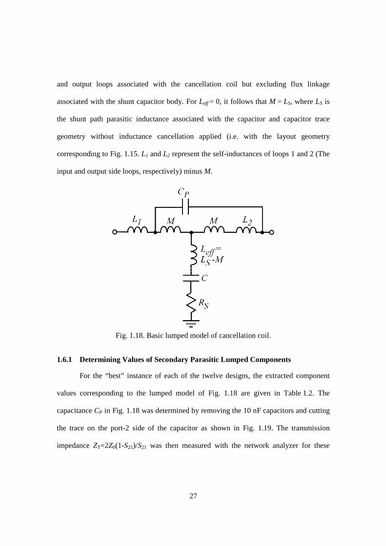
and output loops associated with the cancellation coil but excluding flux linkage
associated with the shunt capacitor body. For Leff = 0, it follows that M = LS, where LS is
the shunt path parasitic inductance associated with the capacitor and capacitor trace
geometry without inductance cancellation applied (i.e. with the layout geometry
corresponding to Fig. 1.15. L1 and L2 represent the self-inductances of loops 1 and 2 (The
input and output side loops, respectively) minus M.
Fig. 1.18. Basic lumped model of cancellation coil.
1.6.1 Determining Values of Secondary Parasitic Lumped Components
For the “best” instance of each of the twelve designs, the extracted component
values corresponding to the lumped model of Fig. 1.18 are given in Table 1.2. The
capacitance CP in Fig. 1.18 was determined by removing the 10 nF capacitors and cutting
the trace on the port-2 side of the capacitor as shown in Fig. 1.19. The transmission
impedance ZT=2Z0(1-S21)/S21 was then measured with the network analyzer for these

28
modified boards. The parasitic capacitances were then calculated from the linear regions
of the |ZT| versus frequency measurements by,
T1/ (2 )PC f Zπ= . (1.3)
Fig. 1.19. Example of how traces were cut to determine CP.
The parameter Leff was assumed to be zero because FASTHENRY predicts that
Leff is close to zero for these designs and the tolerances of construction and modeling do
not allow for a more accurate prediction. The parameter M was thus taken to be the
mutual inductance computed using FASTHENRY for the capacitor filter without a
cancellation loop, or LS as listed in Table 1.2. Parameters L1 and L2 were determined by
modifying the FASTHENRY simulations so that the input and output ports were on the
perimeter of the cancellation coil. Then these inductances were calculated from the
simulation inductance matrices as L1 = L11 – LS and L2 = L22 – LS. The parameter RS was
approximated as 50 mΩ.

29
Table 1.2. Parasitic Capacitances Measured with Network Analyzer and Lumped Model Inductances Calculated with FASTHENRY
Design Parameter Value
CP (pF) L1 (nH) L 2 (nH) LS (nH)
U1 a=16 mm 1.65 4.55 15.49 1.86 U2 a=23 mm 1.63 4.57 14.43 1.25 U3 a=6 mm 0.65 3.03 9.19 1.18 U4 a=6 mm 0.60 2.85 6.59 1.18 U5 a=3.524 mm 0.16 5.00 5.69 0.84
U6 a=2.024 mm 0.16 3.57 4.31 0.84 U7 s=0.2mm 0.47 4.89 6.08 1.25 G1 a=10 mm 1.35 2.66 9.39 1.25 G2 a=9.5 mm 1.69 3.17 9.18 1.86 G3 a=6.5 mm 0.32 3.01 6.82 0.84 G4 a=12 mm 0.78 3.73 8.25 1.25 G5 a=9 mm 0.26 6.21 7.56 1.25
1.6.2 Lumped Model Simulations of Designs
This lumped model was used to model the insertion gains of the “best” instances
of each of the twelve designs presented in this paper. The lumped models were analyzed
in LTspice by performing an AC analysis of the circuit in Fig. 1.18 with source and load
resistances of 50 Ω and a source amplitude of 1 volt. Then the insertion gain (equivalent
to S21) was taken to be twice the magnitude of the load voltage. A comparison of the
insertion gains predicted by the lumped model implemented in LTspice and the measured
insertion gains for each of the designs with a rectangular hole in the ground plane, G1 to
G5, is given in Fig. 1.20. Likewise, similar comparisons for the designs with a solid
ground plane, U1 to U7, are given in Fig. 1.21.

30
Fig. 1.20. Comparison of measured (bold) and lumped model (dashed) insertion gain curves for each of designs with rectangular hole in ground plane.

31
Fig. 1.21. Comparison of measured (bold) and lumped model (dashed) insertion gain curves for each of designs with solid ground plane.

32
1.7 Conclusion
Small PCB trace coils have been used to cancel the parasitic mutual inductance of
surface mount filter capacitors. These coils were implemented on 1.6 mm and 0.79 mm
thick double-sided printed circuit boards. Working from the basic design types shown in
Fig. 1.5 and using an inductance extraction tool such as FASTHENRY, shunt capacitor
filters can be optimized to be effective from MHz to GHz frequencies. A number of
practical designs are presented matching simulation results with measurements, but the
techniques used to produce these designs can easily be used to make inductance
cancellation coils for arbitrary surface mount capacitor filter implementations. The
lumped model presented in Fig. 1.18 provides an additional tool for understanding and
analyzing the secondary parasitics limiting the high frequency performance of a shunt
capacitor filter utilizing a cancellation coil.
References
[1] T. Fischer, C. Kneuer, M. Albach, and G. Schubert, “Mutual Inductance of Capacitor Low-Pass Filters,” in 2009 20th International Zurich Symposium on Electromagnetic Compatibility, 2009, pp. 381–384.
[2] T. M. Zeeff, T. H. Hubing, T. P. Van Doren, and D. Pommerenke, “Analysis of simple two-capacitor low-pass filters,” IEEE Trans. Electromag. Compat., vol. 45, no. 4, pp. 595–601, Nov. 2003.
[3] T. M. Zeeff, A. Ritter, T. H. Hubing, and T. Van Doren, “Analysis of a Low-Pass Filter Employing a 4-Pin Capacitor,” IEEE Trans. Electromag. Compat., vol. 47, no. 1, pp. 202–205, Feb. 2005.
[4] C.-W. Lam, “Methods and Systems for Filtering Signals,” U.S. Patent US 7,417,869 B12008.
[5] H.-F. Chen and K.-H. Lin, “Sensitivity analysis for planar self-coupled windings to reduce parasitic inductance of three-capacitor EMI filters,” in 2009 Asia Pacific Microwave Conference, 2009, vol. 1, pp. 1258–1261.

33
[6] H. Chen, C. Yeh, and K. Lin, “A Method of Using Two Equivalent Negative Inductances to Reduce Parasitic Inductances of a Three-Capacitor EMI Filter,” IEEE Trans. Power Electron., vol. 24, no. 12, pp. 2867–2872, Dec. 2009.
[7] X. Gong and J. A. Ferreira, “Three-dimensional Parasitics Cancellation in EMI Filters with Power Sandwich Construction Three-dimensional coupling,” in Power Electronics and Applications (EPE 2011), Proceedings of the 2011-14th European Conference on, 2011, pp. 1–10.
[8] T. C. Neugebauer and D. J. Perreault, “Filters With Inductance Cancellation Using Printed circuit board transformer,” IEEE Trans. Power Electron., vol. 19, no. 3, pp. 591–602, 2004.
[9] T. C. Neugebauer, J. W. Phinney, and D. J. Perreault, “Filters and Components With Inductance Cancellation,” IEEE Trans. Ind. Appl., vol. 40, no. 2, pp. 483–491, Mar. 2004.
[10] D. J. Perreault, T. C. Neugebauer, and J. W. Phinney, “Filter Having Parasitic Inductance Cancellation,” U.S. Patent 7,242,2692007.
[11] D. J. Perreault, J. W. Phinney, and T. C. Neugebauer, “Filter Having Parasitic Inductance Cancellation,” U.S. Patent 6,937,1152005.
[12] D. J. Perreault and B. J. Pierquet, “Method and Apparatus to Provide Compensation for Parasitic Inductance of Multiple Capacitors,” U.S. Patent 7,589,6052009.
[13] B. J. Pierquet, T. C. Neugebauer, and D. J. Perreault, “A Fabrication Method for Integrated Filter Elements With Inductance Cancellation,” IEEE Trans. Power Electron., vol. 24, no. 3, pp. 838–848, Mar. 2009.
[14] B. J. Pierquet, T. C. Neugebauer, and D. J. Perreault, “Inductance Compensation of Multiple Capacitors With Application to Common- and Differential-Mode Filters,” IEEE Trans. Power Electron., vol. 21, no. 6, pp. 1815–1824, Nov. 2006.
[15] G. Spiazzi and S. Buso, “A practical method for achieving inductance cancellation in filter capacitors,” in 2008 IEEE Power Electronics Specialists Conference, 2008, pp. 885–890.
[16] H. Yoshidome, T. Maruyama, and K. Hirota, “Inductance Cancelled Condensor Implemented Apparatus,” U.S. Patent 5,761,0491998.
[17] B. J. Pierquet, T. C. Neugebauer, and D. J. Perreault, “A Fabrication Method for Integrated Filter Elements With Inductance Cancellation,” IEEE Trans. Power Electron., vol. 24, no. 3, pp. 838–848, Mar. 2009.
[18] S. Wang, F. C. Lee, and W. G. Odendaal, “Cancellation of Capacitor Parasitic Parameters for Noise Reduction Application,” IEEE Trans. Power Electron., vol. 21, no. 4, pp. 1125–1132, Jul. 2006.

34
[19] M. Kamon, M. J. Tsuk, and J. K. White, “FASTHENRY : A Multipole- Accelerated 3-D Inductance Extraction Program,” IEEE Trans. Microw. Theory Tech., vol. 42, no. 9, pp. 1750–1758, 1994.

35
2 A COMPACT IMPLEMENTATION OF PARASITIC INDUCTANCE CANCELLATION FOR SHUNT CAPACITOR FILTERS ON MULTILAYER
PCBS
Abstract
A recent paper by the authors, “Parasitic Inductance Cancellation for Surface
Mount Shunt Capacitor Filters,” described the integration of PCB trace coils with surface
mount capacitors to reduce the negative effects of capacitor parasitic inductance on the
high frequency filtering performance of shunt capacitor filters. This paper introduces a
similar but more compact design that makes use of magnetic coupling between vias as
well as coplanar traces for use on PCBs with more than 2 layers. Implementations of the
design are shown to exhibit similar filtering performance to comparable implementations
of previously published designs while requiring nearly 40% less board area. Additionally,
implementations of the design are demonstrated to be effective in the practical situation
of filtering noise due to crosstalk on a four layer board.
2.1 Introduction
A number of recent papers have demonstrated and analyzed methods for
improving the high frequency performance of shunt capacitor filters by cancelling the
parasitic inductance of the capacitor [1]–[12]. The parasitic inductance of a surface
mount capacitor is highly dependent on the layout of the capacitor on the printed circuit
board (PCB). The basic idea of inductance cancellation is to introduce a precise amount
of mutual inductance between the conductors on each side of a shunt capacitor so that the
total mutual inductance between the input and output loops of the shunt capacitor filter is
zero. By the transformer T-equivalent theorem, this zeroing of the mutual inductance

36
between the input and output loops is equivalent to zeroing the effective shunt path
inductance associated with the capacitor. The use of inductance cancellation for
improving the high frequency performance of filters is an alternative to more
conventional methods like using feed-through capacitors or paralleling multiple
capacitors.
The authors’ recent paper, [4], provides a more in depth review of the theory
behind inductance cancellation as well as its application to surface mount shunt capacitor
filters. This previous paper investigated numerous inductance cancellation filter designs
for surface-mount multilayer ceramic capacitors (MLCCs) using coplanar traces. This
paper extends the work in [4] by presenting an improved design for the integration of
cancellation coils with surface mount MLCCs on practical circuit boards that have a solid
ground plane. The design presented here makes use of magnetic coupling between
neighboring vias as well as coplanar traces, leading to a more compact design relative to
those presented in [4]. This new compact inductance cancellation design will be referred
to in this paper as the coupled via design. Additionally, the new design is advantageous in
that it does not require gapping the ground plane of the circuit board. Closely spaced vias
provide some of the mutual inductance needed for cancellation of the capacitor parasitic
inductance. The work here differs from the works of other researchers on inductance
cancellation schemes in [1]–[3], [5]–[12] in that it employs capacitors with a much
smaller physical size and is effective at much higher frequencies.

37
2.2 Proposed Design and Rationale
A diagram of the proposed design is shown in Fig. 2.1. Note that there are two
pairs of neighboring vias from the top to the bottom layer that contribute to the
cancellation mutual inductance. These contributions can be intuitively visualized by
observing that a current flowing in from Port 1 (P1) and through the capacitor to the
ground plane induces an EMF in each of the vias on the Port 2 (P2) side of the capacitor
that cause a current to flow from Port 2 towards the ground plane (by Lenz’s Law).
Additionally, the section of coplanar traces on the bottom layer and the shorter section on
the top layer above the capacitor also contribute to the mutual cancellation inductance.
The mutual cancellation inductance of the coplanar traces generally decreases for
decreasing distance between the traces and the ground/power plane and for increasing
trace width. The mutual cancellation inductance between the vias likewise decreases with
increased via spacing.
Fig. 2.1. Parameterized layout of proposed design using inductive coupling between vias and coplanar traces to implement cancellation of capacitor parasitic inductance.
Additionally, the inductive coupling between the current into Port 1 and the
current in the capacitor body is beneficial for the reduction of the parasitic inductance.

38
This form of inductive coupling between a trace and the capacitor body for reducing the
negative effects of surface mount capacitor parasitic inductance is described in [13].
Complete cancellation of the parasitic inductance with such coupling, however, is not
very practical for surface-mount capacitors because the magnetic field due to the initial
Port 1 trace that wraps around the capacitor body would need to be equal and opposite to
the magnetic field that wraps around the capacitor body due to current flowing through
the capacitor body itself. The “end tapped” designs described in [6] implement complete
inductance cancellation for large through-hole capacitors using a similar form of
magnetic coupling by having one turn of a coil in series with the shunt path of the
capacitor that couples to many turns of another coil, but these designs were shown in that
paper to be volumetrically inefficient.
There is not a ground plane parallel to the direction of current flow in the vias so a
substantial amount of mutual inductance can be obtained in the small distance in which
the vias are coupled without the need to gap the ground plane (except for the keep-out
region around the vias that allows them to penetrate the ground plane without making
electrical contact). An additional theoretical benefit of the proposed design is that the
ground plane separates halves of the cancellation coils and prevents magnetic coupling
from occurring where it is not beneficial. This design is intended for PCB configurations
with solid ground (and possibly power) plane(s) in between the signal layers on the top
and bottom of the PCB.

39
2.3 Design Procedure
The partial element equivalent circuit (PEEC) method inductance extraction
program FASTHENRY [14] is used to determine the mutual inductance between the two
ports (i.e. L21 of the inductance matrix). In these simulations, the vias are approximated as
solid conductors of square cross section with side length equal to the diameter of the
actual via holes divided by 1.18 [15]. The capacitor is approximated as a copper
conductor of nearly the same dimensions as the actual capacitor package in these
simulations. Thus when L21 of an arrangement of a cancellation coil and a capacitor is
computed as zero, cancellation of the capacitor parasitic inductance is achieved.
FASTHENRY assumes constant currents in linear filament segments, so more accurate
predictions for optimal geometries could potentially be obtained with full wave 3D
electromagnetic numerical methods like the finite element method or method of moments
at the cost of increased computation time.
The nodes in the FASTHENRY simulation geometry associated with the
capacitor body are placed at half the height of the top of the capacitor body above the top
of the traces. A segment with width and height equal to the corresponding dimensions of
the actual capacitor minus 0.1 mm (representing an estimation of the thickness of the
insulation) connects these two nodes. Vertical segments with width equal to the width of
the capacitor body and thickness equal to 0.4 mm (an estimate of the average thickness of
the solder and metal connectors making electrical connection with the MLCC plates) for
the 0603 capacitor model connect the PCB trace to the nodes at half the height of the
capacitor in these simulations. For the FASTHENRY simulation results presented in this

40
paper, the number of filaments assigned to the cross-sections of segments and ground
planes was three plus seven times the length of that dimension in millimeters, rounded
down. For example, a trace that is 0.762 mm wide and 35 µm thick has a cross section
that is discretized into 8×3 filaments. Discretizing conductor segments into separate
filaments is necessary to properly model the influence of skin and proximity effects on
the inductance matrix.
Parametric sweeps of simulations were used to determine the optimal design
parameters. Specifically, the procedure used is outlined as follows:
(1) Validate and/or develop capacitor models by measuring and simulating
parasitic inductance of simple conventional shunt capacitor filter
arrangements.
(2) Create FASTHENRY input file template describing the parameterized
geometry with two ports.
(3) Validate filament densities chosen by performing simulations with several
higher filament densities and checking for convergence at the frequencies of
interest.
(4) Determine which parameters of the layout are fixed constraints and which are
variable.
(5) Perform simulations of a sweep through the variable parameter values within
their practical range to determine a desirable combination of variable
parameter values. Each simulation should be performed at a high frequency
(200 MHz was used in this work).

41
(6) If there is no zero crossing of a mutual inductance vs. parameter values plot,
repeat the process, varying additional parameters, or select a parameter
combination resulting in a nearly zero mutual inductance.
Modeling the inductance of an inductance cancellation-based filter fairly
accurately is important. If the parasitic inductance is overcompensated, the effective
shunt path impedance magnitude increases with increasing cancellation mutual
inductance so the performance can actually be worse than that of a conventional shunt
capacitor filter. However, the measurements in [4] demonstrate that even when the
coplanar cancellation traces are lengthened or shortened by about 30% compared to the
optimal value, the resulting insertion gains are still improved relative to a conventional
shunt capacitor filter.
2.3.1 Validation of Capacitor Model
For boards with a small distance between the signal layer and the ground plane, as
is common on multilayer PCBs, how the capacitor is modeled can make a big difference
in how much parasitic inductance is calculated. In order to validate the simulation model
of the capacitor described previously, several conventional shunt capacitor filter boards
with the layout shown in Fig. 2.2 were constructed. They were built using a PCB milling
machine from double-sided copper clad FR4 boards. These boards were 35 mm long and
25 mm wide and had the following parameter values: w=0.762 mm, wc=0.762 mm, and
dcv=0.8 mm. The measured parasitic inductances of these boards were compared with
those of equivalent models simulated in FASTHENRY at a frequency of 60 MHz. For
each board, the measured parasitic inductance was determined from the measured self-

42
resonant frequency, f0, and the measured capacitance, C, (after soldering the capacitor on
the board and allowing it to cool to room temperature) by,
2 201/ (4 )SL Cfπ= . (2.1)
The self-resonant frequency, f0, was determined from the minimum of 1601
linearly spaced |S21| measurement points between 300 kHz and 300 MHz.
Fig. 2.2. Layout of conventional single shunt capacitor filter arrangement for measurements and simulations.
All capacitors used for the measurements were 5% tolerance X7R MLCC 10 nF
capacitors with a 0603 package. All vias used to make the boards for these measurements
were hollow 0.8 mm outer diameter copper rivets designed for PCB prototyping. The
measured and simulated results are listed in Table 2.1 for boards with a total thickness
(including 35 µm thick copper on both sides) of 0.79 mm and 0.32 mm. These results
show that the capacitor models used are reasonable approximations.
Table 2.1. Comparison of Measured and Simulated Parasitic Inductances of Conventional Shunt Capacitor Filters
Total board thickness (mm)
lc (mm)
Measured LS (nH)
Simulated LS (nH)
0.32 2.4 0.6149 0.5788 0.79 2 0.6736 0.7051 0.79 2.4 0.7728 0.8432 0.79 2.5 0.7921 0.8793 0.79 3 1.0285 1.0607

43
2.4 Implementation on a Three Layer PCB
In order to be able to directly compare the performance and board area
requirements of an implementation of this design with some of the designs in [4],
implementations of the coupled via design were made with a milling machine and a
0.79 mm thick double-sided copper clad FR4 board stacked on top of a 0.76 mm thick
single-sided copper clad FR4 board to form a three layer board with a ground plane in the
center. The capacitors used were 10 nF MLCCs with a 0603 package. The following
parameters from Fig. 2.1 were considered fixed for purposes of comparison to some of
the designs in [4]: lc=2.4 mm, s=0.25 mm, w=0.762 mm, wc=0.762 mm, sc=0.25 mm, and
dcv=0.8 mm. The copper layers are all 35 µm thick. The via diameter was dv=0.36 mm.
The ground plane was removed to a distance of 0.4 mm from the outside of the via holes
(except for the capacitor via hole) in both simulations and physical implementations.
Results of a parametric sweep of FASTHENRY simulations at 200 MHz over a
variety of distances between neighboring vias (parameter sv in Fig. 2.1) for this
implementation of the coupled via design are shown in Fig. 2.3. This figure suggests that
the optimum spacing between the vias is about 0.725 mm.

44
Fig. 2.3. FASTHENRY simulations of the effect of via spacing on overall mutual inductance of 0603 package shunt capacitor with coupled via inductance cancellation
implemented on a three-layer board.
Implementations of the design were built with 0.65 mm, 0.70 mm, 0.75 mm, and
0.80 mm spacings between vias. The capacitor via was implemented using 0.8 mm outer
diameter copper rivets in 0.8 mm diameter holes and the other vias were implemented
using 0.4 mm holes filled with 0.36 mm diameter (27 AWG) copper wire bent over and
cut off about 0.3 mm above the top and bottom surfaces of the stacked boards and
soldered in place while the two boards were clamped together. As evident from the plot
of the measured insertion gains in Fig. 2.4, the coupled via design with 0.70 mm via
spacing showed the best insertion gain at high frequencies. All insertion gains presented
in this paper were measured with a network analyzer with 50 Ω ports that was calibrated
using the short-open-load technique.

45
Fig. 2.4. Measured insertion gains of coupled via inductance cancellation filter design implementations on three layer boards with 0603 10 nF capacitors.
Fig. 2.5 compares the measured insertion gain of the implementation with
sv=0.70 mm to that of a comparable conventional single capacitor filter (as shown in Fig.
2.2) as well as to the insertion gains of the optimized comparable designs presented in
[4]. These comparable designs use the same capacitors and have the same distance
between the ground plane and the top layer, the same trace width (w), the same capacitor
via diameter (dcv), and the same capacitor trace length (lc) as the implementation of the
coupled via design. The coupled via inductance cancellation design exhibits similar high
frequency filtering to the comparable designs in [4].

46
Fig. 2.5. Comparison of implementation of coupled via design to a comparable conventional shunt capacitor filter and comparable implementations of previously published designs (G3, U5, and U6 from [4] which are shown as dotted curves).
However, this implementation of the coupled via design requires nearly 40% less
board area than the most compact of the previously published optimized designs that had
comparable design parameter values. Fig. 2.6 shows how the board areas were computed
and gives a quantitative comparison of the area requirements of the inductance
cancellation designs whose insertion gains are shown in Fig. 2.5. The interior of the
dashed red boundaries are the regions that are considered to count towards board area for
the top layer of these designs and the dashed green boundaries represent the regions that
are considered to count toward board area for the bottom layer of these designs. Note that

47
the large gap in the ground plane for design G3 is not counted towards the area of this
design so as to have a conservative measure of area.
Fig. 2.6. Comparison of total board area requirements of the new coupled via design and the optimized sizes of the previously published designs G3, U5, and U6 from [4]. The red and green dashed boundaries show which regions are counted toward the board area on
the top and bottom layers, respectively.
2.5 Implementation on a Four-Layer PCB
Coupled via inductance cancellation designs were also implemented on
commercially fabricated four-layer boards. These boards were 29.8 mm long × 19.7 mm
wide and consisted of the following copper layers and dielectric substrates: top layer
copper, 0.31 mm FR4, ground plane copper, 0.711 mm FR4, power plane copper,
0.31 mm FR4, and bottom layer copper. All copper layers were 35 µm thick. For each
board, the connection of the SMA connectors to the ground plane was made with an array
of 10 vias on each side in order to provide a low inductance path. Four 0.1 µF decoupling
capacitors with 0805 packages connected the power plane and ground plane through vias

48
near the four corners of the board. The coupled via inductance cancellation filter was
placed near the center and employed a 10 nF capacitor with a 0603 package. For these
coupled via inductance cancellation design implementations, the following parameter
values were used: lc=2.4 mm, s=0.25 mm, w=0.762 mm, wc=0.762 mm, sc=0.25 mm, and
dcv=0.356 mm. Additionally, the via spacing, sv, was varied and two different via
diameters were used: dv=0.203 mm and dv=0.356 mm.
In the FASTHENRY simulations of these designs, the ground reference nodes at
each port were made electrically equivalent to the proximal points of the power plane.
FASTHENRY simulations showing parametric sweeps of via spacing for two different
via diameters for this configuration are shown in Fig. 2.7.
Fig. 2.7. FASTHENRY simulations of the effect of via spacing for two different via diameters on overall mutual inductance of coupled via inductance cancellation filter on a
four-layer board.
Measured results comparing the insertion gains with different via diameters (dv)
and via spacings (sv) to the insertion gain of a conventional shunt capacitor with the same
values for parameters lc, wc, and dcv on the same type and size of four-layer board are
shown in Fig. 2.8. All of the coupled via filter designs in this figure perform better than

49
the comparable conventional shunt capacitor filter and the implementation with
0.203 mm diameter vias spaced 0.762 mm apart exhibits the best high frequency
performance.
Fig. 2.8. Comparison of insertion gains of commercially fabricated four layer board implementations of the coupled via design with different via diameters (dv) and spacings (sv) to the insertion gain of a comparable conventional shunt capacitor filter on the same
type of four layer board. All filter capacitors are 10 nF 0603 capacitors.
2.6 Example Application to I/O Filtering
The insertion gains measured with the network analyzer represent the
performance of the filter in a 50 Ω system, which may be different from the performance
in actual systems. To demonstrate the effectiveness of the coupled via inductance
cancellation filter in a system with a practical noise source impedance, four different
four-layer boards with the same layer configuration as those described in the previous
section were built. These boards employed shunt capacitor filter configurations with or

50
without inductance cancellation to filter noise due to crosstalk. In these boards, a trace
connects the output of a 3.3 V crystal oscillator generating a 50 MHz square wave with
fast rise times to a 15 pF capacitor load. This aggressor trace is routed next to a victim
trace that is terminated in a board-edge SMA connector (which also connects to the
ground plane through vias). Both of these traces are 0.762 mm wide and are separated by
0.25 mm for a total coupling distance of about 3.3 cm. Fig. 2.9 shows a block diagram of
this test setup.
Fig. 2.9. Block diagram of setup demonstrating application of coupled via inductance cancellation to I/O filtering.
These four boards are identical in layout except that two of the boards have
conventional shunt capacitor filters and two of them have implementations of the coupled
via inductance cancellation filter design with 0.203 mm diameter vias spaced 0.762 mm
apart next to the SMA connector. Furthermore, two of the boards have the end of the
victim trace that is not terminated in an SMA connector connected directly to the 3.3 V
power plane (VDD) and two of the boards have this end of the victim trace connected to
the CMOS output of a microcontroller which is generating a 40 kHz square wave. Table

51
2.2 summarizes the differences between these four boards and assigns a letter code to
each of them.
Table 2.2. Summary of Different Boards Tested and Letter Codes Assigned to Each
Victim trace connected to CMOS output; 1 nF
filter capacitor
Victim trace connected to VDD; 100 nF filter
capacitor Conventional shunt
capacitor filter Board A Board B
Coupled via inductance
cancellation filter Board C Board D
The SMA connector of the boards is connected to a Rohde and Schwarz FSL
spectrum analyzer that is set up with a resolution bandwidth of 100 kHz, peak detection,
and averaging over five sweeps from 10 MHz to 3 GHz. The boards are powered by a
3.3 V power supply and have five decoupling capacitors totaling 3.2 µF spread around
the board. Fig. 2.10 and Fig. 2.11 compare the coupled noise measured on the board with
the coupled via parasitic inductance cancellation filter design to that of the board using a
shunt capacitor in a conventional arrangement. Fig. 2.10 compares the measured spectra
for boards B and D while Fig. 2.11 compares the measured spectra for boards A and C.
Note that the filter using inductance cancellation is more effective than the conventional
shunt capacitor configuration at frequencies in the hundreds of megahertz.

52
Fig. 2.10. Comparison of measured spectrum of noise measured from board D (coupled via inductance cancellation-based filter) and board B (conventional shunt capacitor
filter). These two boards have one end of the victim trace connected to VDD.
Fig. 2.11. Comparison of measured spectrum of noise measured from board C (coupled via inductance cancellation-based filter) and board A (conventional shunt capacitor
filter). These two boards have one end of the victim trace connected to a CMOS output of a microcontroller outputting a 40 kHz square wave.

53
For comparison purposes, the noise spectra of the four different boards were also
measured with the filter capacitors removed. These results are presented in Fig. 2.12 for
the boards with the victim trace terminated to VDD (B and D) and in Fig. 2.13 for the
boards with the victim trace terminated to the microcontroller CMOS output (A and C).
These measurements verify that the boards with the same victim trace terminations and
with the filter capacitors removed exhibit very similar spectral peaks.
Fig. 2.12. Measured spectra of boards with one end of the victim trace connected to VDD with filter capacitors removed.

54
Fig. 2.13. Measured spectra of boards with one end of the victim trace connected to the CMOS output of a microcontroller with the filter capacitors removed.
2.7 Conclusion
A compact shunt capacitor parasitic inductance cancellation design using
inductive coupling between via pairs as well as coplanar traces is introduced. An
implementation of this new design requires about 40% less area than the most compact
comparable design demonstrated in [4] while exhibiting similar filtering performance.
The design is implemented on three and four layer PCBs and is effective in a 50 Ω
system as well as in practical situations of filtering noise on an output trace due to cross
talk.
References
[1] H.-F. Chen and K.-H. Lin, “Sensitivity analysis for planar self-coupled windings to reduce parasitic inductance of three-capacitor EMI filters,” in 2009 Asia Pacific Microwave Conference, 2009, vol. 1, pp. 1258–1261.

55
[2] H. Chen, C. Yeh, and K. Lin, “A Method of Using Two Equivalent Negative Inductances to Reduce Parasitic Inductances of a Three-Capacitor EMI Filter,” IEEE Trans. Power Electron., vol. 24, no. 12, pp. 2867–2872, Dec. 2009.
[3] X. Gong and J. A. Ferreira, “Three-dimensional Parasitics Cancellation in EMI Filters with Power Sandwich Construction Three-dimensional coupling,” in Power Electronics and Applications (EPE 2011), Proceedings of the 2011-14th European Conference on, 2011, pp. 1–10.
[4] A. J. Mcdowell and T. H. Hubing, “Parasitic Inductance Cancellation for Surface Mount Shunt Capacitor Filters,” IEEE Trans. Electromag. Compat., vol. 56, no. 1, pp. 74–82, Feb. 2014.
[5] T. C. Neugebauer and D. J. Perreault, “Filters With Inductance Cancellation Using Printed circuit board transformer,” IEEE Trans. Power Electron., vol. 19, no. 3, pp. 591–602, 2004.
[6] T. C. Neugebauer, J. W. Phinney, and D. J. Perreault, “Filters and Components With Inductance Cancellation,” IEEE Trans. Ind. Appl., vol. 40, no. 2, pp. 483–491, Mar. 2004.
[7] D. J. Perreault, T. C. Neugebauer, and J. W. Phinney, “Filter Having Parasitic Inductance Cancellation,” U.S. Patent 7 242 269, 2007.
[8] D. J. Perreault, J. W. Phinney, and T. C. Neugebauer, “Filter Having Parasitic Inductance Cancellation,” U.S. Patent 6 937 115, 2005.
[9] D. J. Perreault and B. J. Pierquet, “Method and Apparatus to Provide Compensation for Parasitic Inductance of Multiple Capacitors,” U.S. Patent 7 589 605, 2009.
[10] B. J. Pierquet, T. C. Neugebauer, and D. J. Perreault, “A Fabrication Method for Integrated Filter Elements With Inductance Cancellation,” IEEE Trans. Power Electron., vol. 24, no. 3, pp. 838–848, Mar. 2009.
[11] B. J. Pierquet, T. C. Neugebauer, and D. J. Perreault, “Inductance Compensation of Multiple Capacitors With Application to Common- and Differential-Mode Filters,” IEEE Trans. Power Electron., vol. 21, no. 6, pp. 1815–1824, Nov. 2006.
[12] B. J. Pierquet, T. C. Neugebauer, and D. J. Perreault, “A Fabrication Method for Integrated Filter Elements With Inductance Cancellation,” IEEE Trans. Power Electron., vol. 24, no. 3, pp. 838–848, Mar. 2009.
[13] H. Yoshidome, T. Maruyama, and K. Hirota, “Inductance Cancelled Condensor Implemented Apparatus,” U.S. Patent 5 761 049, 1998.
[14] M. Kamon, M. J. Tsuk, and J. K. White, “FASTHENRY : A Multipole- Accelerated 3-D Inductance Extraction Program,” IEEE Trans. Microw. Theory Tech., vol. 42, no. 9, pp. 1750–1758, 1994.

56
[15] C. Balanis, Antenna Theory, 2nd ed. New York: John Wiley & Sons, Inc., 1997, pp. 454–456.

57
3 DECOMPOSITION OF SHIELDING EFFECTIVENESS INTO ABSORPTION AND REFLECTION COMPONENTS
Abstract
Plane wave shielding effectiveness is frequently expressed as the sum of three
terms called penetration loss, reflection loss, and an internal reflections correction term.
This well-known decomposition was originally developed by Schelkunoff, and provides
an intuitive way of relating material properties to the overall shielding effectiveness of
certain shielding materials, especially metallic materials. In experimentally characterizing
the shielding effectiveness of composite materials, other methods of describing the
reflection and absorption contributions to shielding are commonly used. These other
decompositions are generally more closely related to the reflected and absorbed power
densities and are thus easier to obtain from measurements. This paper analyzes different
decompositions that have been used to describe the shielding properties of materials. It
introduces the term mismatch decomposition to describe a method for decomposing
shielding effectiveness into terms related to the reflectance and absorptance of a material.
This decomposition method has been effectively applied by a number of researchers, but
inconsistent terminology has prevented the full value of this decomposition from being
recognized. The mismatch decomposition results in terms that are useful as figures of
merit because they are closely related to the reflected and absorbed power and are readily
derived from standard measurements of plane wave shielding effectiveness.

58
3.1 Introduction
Electromagnetic shielding plays an important role in ensuring the electromagnetic
compatibility (EMC) of many electronic systems. Shields have traditionally been
constructed from metals and metal coatings, but this approach to shielding can be
expensive and/or heavy [1]. The need for lightweight and inexpensive shielding materials
has driven a large amount of research in recent years on the shielding properties of
polymer composites and intrinsically conductive polymers [2]–[19]. Additionally, it is
often desirable for a shield to absorb a large amount of energy relative to the energy that
it reflects so that secondary electromagnetic pollution is minimized [3], [5], [8], [20]–
[22]. Thus quantifying the reflection and absorption contributions to shielding is
important in many applications.
The shielding properties of materials are typically quantified by measuring the
electromagnetic shielding effectiveness (EMSE) of a flat material sample with a given
thickness. The EMSE is the insertion loss expressed in decibels of the sample in free
space with a normally incident plane wave. In recent books on EMC (for example [23]–
[28]), plane wave shielding is typically presented in a model known as the transmission
line model of shielding. This model of shielding was originally developed by Schelkunoff
[29]–[31]. Schelkunoff analyzed the EMSE of planar, cylindrical, and spherical shields
by using wave impedances in a manner analogous to transmission line characteristic
impedances. He applied the transmission line concepts of reflection and transmission
coefficients to the shielding analysis. The transmission line model of shielding gives an
exact solution for the EMSE of an infinite homogeneous material sheet or layers of sheets

59
with a normally-incident plane wave. However, the transmission line model of shielding
gives only approximate solutions in situations with non-plane waves, for example a near
field source next to a planar shield, or the cylindrical and spherical shields that
Schelkunoff analyzed. For approximate application of the transmission line model to
situations with non-plane waves, the wave impedance must be selected carefully to
achieve good accuracy [28], [32]–[34]. The transmission line model of shielding is also
applicable to composite materials using effective constitutive parameters when the
heterogeneities are evenly dispersed and are small compared to the effective wavelength
in the medium [35]. Section 3.2 of this paper reviews the transmission line model of
shielding.
The transmission line model of shielding breaks up the decibel value of EMSE
into the sum of three decibel loss terms: penetration loss (also called absorption loss),
reflection loss, and an internal reflections correction term (also called multiple reflections
loss) as illustrated in (3.1).
Internal reflections
correction
Schelkunoff decomposition of shielding effectiveness (terms in dB)
Penetration loss / Reflection lossabsorpti termon loss
SE A BR= + +
(3.1)
This decomposition of EMSE will be referred to in this paper as the Schelkunoff
decomposition. Additionally, the sum of reflection loss and the internal reflections
correction term will be referred to in this paper as the net reflection loss. The internal
reflections correction term is generally negligible for thick good conductors; but for poor
conductors, thin metallic films, or shielding at low frequencies, it can have a large
negative value. In EMC textbooks, graphs of the EMSE of materials decomposed into the

60
terms of the Schelkunoff decomposition are commonly presented. Although the
Schelkunoff decomposition may break EMSE into components that are easy to calculate
and intuitive for understanding the parametric dependence of EMSE, the terms do not
represent very useful figures of merit and they do not correlate to quantities obtained
from shielding effectiveness measurements in a straightforward manner. Section 3.3 of
this paper reviews and analyzes the Schelkunoff decomposition, its physical
interpretations, and its mathematical relationship to network parameters and
reflectance/absorptance.
Even though the terms describing reflection and absorption in the Schelkunoff
decomposition are not closely related to the actual levels of reflected and absorbed
power, terms from the Schelkunoff decomposition have been used to quantify the
reflection and absorption contributions to EMSE in some experiments on materials (for
example [3], [5]). However, other measures have also been used to quantify the reflection
and absorption contributions to shielding. For the analysis of radar absorbing materials, it
is common to use the reflection coefficient expressed in decibels with the absorbing
material backed by a thick metal sheet approximating a perfect electrical conductor as a
specification of the balance of reflection/absorption [3], [36]. A number of recent papers
have used the input reflection coefficient expressed in decibels to quantify reflected
power in shielding experiments [18], [37]. Of course, one could use the linear measures
of reflectance (reflected power density divided by incident power density), transmittance
(transmitted power density divided by incident power density), and absorptance
(absorbed power density divided by incident power density) to describe how much of a

61
material’s shielding is due to reflection and how much is due to absorption. Such
measures are employed in a number of recent shielding experiments [10], [38], [39].
However, it is often desired to have decibel measures of reflection and absorption that
sum to give the total decibel EMSE as the terms in the Schelkunoff decomposition do.
In transmission line engineering, a quantity called the mismatch loss is frequently
used to describe the degree of mismatch in a transmission line at a particular point.
Mismatch loss has been widely used in the analysis of the shielding properties of
composites in recent publications [6], [17], [20], [21], [40]–[45]; although the authors of
these publications used different terminology to describe this loss. Mismatch loss is a
different quantity than the reflection loss or net reflection loss of the Schelkunoff
decomposition. This point is explicitly made in a few of these publications, but confusion
arises from the fact that the decomposition based on mismatch loss is often described
using the same name or notation as the terms in the Schelkunoff decomposition. Some
recent publications incorrectly imply that the mismatch loss is an approximation for the
Schelkunoff reflection loss for good conductors when the internal reflections correction
term is close to zero (for example [21], [43], [45]). The decomposition of EMSE using
mismatch loss and another term called dissipation loss will be referred to in this paper as
the mismatch decomposition. The mismatch decomposition gives terms that are useful as
figures of merit because they are closely related to the absorbed and reflected power.
Furthermore, the mismatch decomposition may be interpreted as a comparison to a
situation of conjugate matching between the source impedance and the equivalent input
or output impedance of the shield transmission line analog terminated with free space.

62
Section 3.4 of this paper reviews and analyzes the mismatch decomposition and
compares it to the Schelkunoff decomposition.
Section 3.5 of this paper provides graphical plots of various EMSE
decompositions computed for three example shields and Section 3.6 concludes the paper.
Additionally, the appendix (referenced in Section 3.3) shows how the Schelkunoff
decomposition can be generalized using image parameters to apply to layered materials.
3.2 Review of Transmission Line Model of Shielding
The basis for the transmission line (TL) model of shielding is that the voltage in a
TL is analogous to the electric field intensity of a plane wave and the current in a TL is
analogous to the magnetic field intensity of a plane wave. Additionally the distributed
series inductance per unit length, shunt capacitance per unit length, and shunt
conductance per unit length of a TL are analogous to the respective constitutive
parameters of permeability, permittivity, and conductivity. These analogies make most
TL concepts directly applicable to the analysis of shielding of normally incident plane
waves.
Fig. 3.1 shows a depiction of the basic plane wave shielding problem of a single-
layered homogeneous and isotropic material that is infinite in the xy-plane but has
thickness t in the z direction. The shield is surrounded by free space with intrinsic
impedance η0 and propagation constant γ0 on either side for z < 0 and z > t. For the
electric and magnetic field intensity vectors expressed as RMS phasors, the complex
Poynting vector is given by *= ×S E H and the time-average Poynting vector is Re(S).
By the nature of a plane wave, the electric and magnetic field vectors are spatially

63
orthogonal, so the cross product of vectors reduces to a multiplication of scalars. The
magnitude of the time-average Poynting vector is the time-average power density (with
units of watts per square meter). Because η0 is real, the time-average power densities
associated with the incident, reflected, and transmitted fields in Fig. 3.1 are given by:
20| | /I IP E η= , 2
0| | /R RP E η= , and 20| | /T TP E η= , respectively. By conservation of
energy,
I R T AP P P P= + + , (3.2)
where PI is the incident power density, PR is the reflected power density, PT is the
transmitted power density, and PA is the absorbed power density. It is more convenient,
however, to consider power densities normalized to the incident power density. Dividing
each term in (3.2) by IP gives the normalized power balance equation,
ˆ ˆ ˆ1 R T AP P P= + + . (3.3)
The following notation and terminology for these power densities normalized to the
incident power density will be used in this paper: is called the reflectance, is called
the transmittance, and is called the absorptance.

64
Fig. 3.1. Basic plane wave shielding problem of homogeneous and isotropic material infinite in xy-plane.
With the permeability µ, the conductivity σ, and the permittivity ϵ potentially
expressed as complex numbers and with ω representing the angular frequency of the
wave, the propagation constant in the material is:
( )j j jγ α β ωµ σ ω= + = + ε . (3.4)
As in (3.4), the propagation constant may be written in terms of the attenuation constant α
and the phase constant β. The intrinsic impedance of the material is:
j
j
ωµησ ω
=+ ε
. (3.5)
Another term important for the analysis of shielding materials is the skin depth,
which is defined as δs = 1/α. In good conductors when the frequency is such that σ ≫ ωϵ,
the intrinsic impedance may be approximated as /jη ωµ σ≈ and the propagation
constant may be approximated as ( )1 / 2jγ ωµσ≈ + . Thus the skin depth in good
conductors can be closely approximated by ( ) 1/2
s fδ π µσ −≈ , where f = ω/(2π).

65
Elementary electric field reflection coefficients are denoted by ρ and represent the ratio of
reflected to incident electric field intensity that would occur at the junction of two
materials if both materials were infinitely thick. Actual reflection coefficients
representing the ratio of electric field intensity in the backward and forward traveling
waves next to a junction are denoted by Γ. The elementary electric field reflection and
transmission coefficients of a normally incident plane wave traveling from free space and
impinging on the material in Fig. 3.1 are given by ( ) ( )1 0 0/ρ η η η η= − + and
( )1 02 /T η η η= + , respectively. Likewise, the electric field reflection and transmission
coefficients of a wave traveling out of the material and into free space are given by
( ) ( )2 0 0/ρ η η η η= − + and ( )2 0 02 /T η η η= + , respectively. The relationships 1 11T ρ= + ,
2 21T ρ= + , and 1 2ρ ρ= − will be used for subsequent derivations in this paper.
The transmitted electric field can be expressed as a sum of the field that would be
transmitted directly through the material, 1 2t
IE eT Tγ− , and the fields that experience
internal partial reflections an even number of times and then are transmitted into the
region z > t of Fig. 3.1. Thus, the transmitted electric field intensity can be expressed as
the following summation of partial reflections:
( )21 1 2 2
0
mt t
T Im
E T TE e eγ γρ ρ∞
− −
=
= −∑ . (3.6)
By converting the electric field intensities represented in (3.6) to power densities, using
the formula for the sum of a convergent geometric series, noting that 21 1 2ρ ρ ρ= − , and
dividing by the incident power density, the transmittance can be expressed as,

66
2
1 22 21
ˆ1
T
I
t
T t
P TT eP
P e
γ
γρ
−
−= =−
. (3.7)
The reflectance is easily found by calculating the input reflection coefficient and
taking the magnitude squared of this value:
( ) 22
2 1
2 21
1ˆ
1
t
R in t
eP
e
γ
γ
ρρ
−
−
−−
== Γ . (3.8)
Consequently, from the power balance relationship, (3.3), the absorptance can be
expressed as,
ˆ ˆ ˆ1A T RP P P= − − . (3.9)
3.3 Schelkunoff Decomposition of Shielding Effectiveness
In general, EMSE can be defined as either the electric or magnetic field insertion
loss expressed in decibels when the material is added [26]. However, for the plane wave
shielding problem shown in Fig. 3.1, this is equivalent to the power insertion loss or
simply the reciprocal of the transmittance expressed in decibels:
( ) 1 210
110 2 2
ˆSE 10log 20log1
t
T t
TT eP
e
γ
γρ
−
−= − = −−
. (3.10)
In the EMC literature, there is widespread decomposition of (3.10) into decibel
quantities called penetration loss, reflection loss, and the internal reflections correction
term that sum to give the EMSE. As described in Section 3.1, this decomposition is called
the Schelkunoff decomposition and can be expressed as,
SE A R B= + + . (3.11)

67
The penetration loss, which is also called absorption loss, is the reciprocal of the
attenuation that occurs when a wave travels through the material once and is the non-
negative quantity given by:
10 1020log 20log ( )· 8.7tA e e t tγ α α−= − = ≈ . (3.12)
The penetration loss can equivalently be physically interpreted as the ratio expressed in
decibels of the magnitude of the incident complex Poynting vector to the magnitude of
the transmitted complex Poynting vector when the shield is simultaneously matched for
no reflection on both sides.
The reflection loss is the reciprocal of the product of the transmission coefficients
at both interfaces expressed in decibels and represents the reduction in transmitted field
that would occur due to reflections off of both interfaces in the absence of loss in the
medium and internal reflections between the two interfaces. Reflection loss is the non-
negative quantity given by:
210 1 2 10 120 log 20log 1R TT ρ= − = − − . (3.13)
The remainder of the expression for EMSE is the correction term for multiple
internal reflections, accounting for the reflections represented by the geometric series in
(3.6). The internal reflections correction term, which is also called the multiple
reflections loss, is given by:
2 210 120 log 1 tB e γρ −= − . (3.14)
68
Because 1 1ρ < , it follows that the upper positive limit of B is about 3 dB which occurs
when 2 21
te jγρ − = ± . For sufficiently thick good conductors at frequencies where t ≫ δs,
the argument of the absolute value function in (3.14) is near unity and 0 dBB ≈ .
The sum of the internal reflections correction term and the reflection loss will be
called the net reflection loss in this paper:
netR R B= + . (3.15)
This net reflection loss thus represents a comparison loss comparing the magnitude of the
ratio of the incident and transmitted complex Poynting vectors of the actual shield
configuration to the corresponding ratio which would occur if the shield was
simultaneously matched.
3.3.1 Determining Decomposition from Scattering Parameters
There are many different techniques that have been used to obtain measurements
approximating plane wave EMSE. Often these measurement techniques make use of
transverse electromagnetic (TEM) cells or coaxial airlines. Analysis of these different
measurement techniques is beyond the scope of this paper, but if one obtains the
necessary complex-valued scattering parameters S11 and S21 of a single-layered shield in
free space, the terms of the Schelkunoff decomposition can easily be obtained. As
presented in [46], the elementary reflection coefficient of a wave impinging on the
material can be found by,
21 1ρ χ χ= ± − , (3.16)
where the solution giving 1 1ρ ≤ is taken and where,

69
2 211 21
11
1
2
S S
Sχ − += . (3.17)
From this result, the propagation term can be determined as,
( )11 21 1
11 21 11t S S
eS S
γ ρρ
− + −=− +
. (3.18)
Then, the penetration loss, the reflection loss, and the internal reflections corrections term
can be found from the results of (3.16) and (3.18) using the formulas in (3.12), (3.13),
and (3.14).
3.3.2 Determining Power Distribution from Decomposition
The full characterization of a reciprocal linear two-port network requires six real-
valued parameters, while a network known to be symmetric may be characterized by four
real-valued parameters. Thus, the three real-valued parameters that are given by the
Schelkunoff decomposition are by themselves insufficient to fully characterize a network.
However, it is often of interest to know simply how much power is reflected and
absorbed by a shield. This raises the question of whether it is possible to determine the
reflectance/absorptance from the Schelkunoff decomposition of a single-layered shield in
different circumstances.
3.3.2.1 Good Conductor Approximation
It is easy to approximate the reflectance/absorptance from the Schelkunoff
decomposition of a shield composed of a good conductor at frequencies when σ ≫ ωϵ.
For good conductors, the magnitude of η is generally very small at frequencies of interest
for EMC. For example, the intrinsic impedance of copper at 1 GHz is 0.0037∠45° Ω and

70
|η| is even lower for f < 1 GHz. Additionally, both the propagation constant and intrinsic
impedance in good conductors have approximately equal real and imaginary parts. These
relationships are evident from the following equation which is valid for materials with
real-valued permeability and conductivity:
( )( )
2 2 2
2 22
Re 1 tan 1
Im 1 tan 1
η δ βαη δ
+ += =+ −
, (3.19)
where tan ( ) / ( )δ ω σ ω′′ ′= +ε ε is the loss tangent (which is very large for good
conductors) and where the complex permittivity is expressed as ϵ = ϵ′ − jϵ″.
Thus the normalized intrinsic impedance (which is denoted by ζ with real part ζr)
can be approximated as,
0 (1/ )r jζ η η ζ += ≈ . (3.20)
With this approximation, the argument of the logarithm in the reflection loss term (which
is denoted by MR) can be expanded as,
2 2/10
2 4 3 2
32410
( 1) 4 8 8 4 1R r
Rr r r r
Mζζ
ζ ζ ζ ζ ζ−= = ≈
+ + + + +. (3.21)
Solving (3.21) for ζr and selecting the correct root (the one giving 0 < ζr < 1 for the
possible interval of 0 < MR ≤ 1 gives,
( )14 2 8 2 2
2r R R R
R
M M MM
ζ ≈ − − − − + + . (3.22)
Then, the elementary electric field reflection coefficient may be approximated as,
1
(1 ) 1
(1 ) 1r
r
j
j
ζρζ
+ −≈+ +
. (3.23)

71
From (3.12), the product of the attenuation constant and thickness may be written
in terms of the Schelkunoff absorption loss as, αt = A/(20 log10(e)). The product of the
propagation constant and thickness may thus be approximated as,
( )1t t jγ α≈ + . (3.24)
Also note that the denominator of (3.8) is 10B/10. Thus the reflectance can be
approximated by substituting 10B/10, γt from (3.24), and 1ρ from (3.23) into (3.8). The
transmittance is = 10/, so the absorptance can be approximated with (3.9).
These approximations are shown to be accurate for a variety of example materials later in
this paper.
3.3.2.2 General Material Solution
For a general single-layered material for which it is only known that the relative
permeability is one, but for which it is not necessarily the case that σ ≫ ωϵ, determining
the reflectance/absorptance from the Schelkunoff decomposition is a more involved
process. For such a material, we can write the intrinsic impedance as
( )0 0 //j j jη ωµ γ ωµ α β= = + . By expressing the reflection coefficient 1ρ in terms of
, ω, α, and β, we can write the arguments of the logarithms in the Schelkunoff
decomposition reflection loss and internal reflections correction terms as the following
two expressions, which both involve entirely real-valued quantities:
( )( )( )
2 2 2 2 20 0/10
22 2 2 2 20 0 0 0
1610
2
Rη µ ω α β
η α β βη µ ω µ ω−
+=
+ ++ and (3.25)
/10 20 0,cos(2 si10 ( , , n(2e ), ), , , )B tf t tαα β β β η µ ω− = , (3.26)

72
where f is a real-valued multivariate rational function.
A nonlinear system of two equations with two unknowns in terms of α and β is
formed by (3.25) and (3.26) with the symbolic substitution made in (3.26) that
t = A/(20 log10(e)⋅α). Although this system is solvable with numerical methods, the
robustness of this procedure was not thoroughly investigated as these formulas are
intended primarily to indicate the theoretical relationships between the Schelkunoff
decomposition and the reflectance/absorptance; furthermore, the approximate method in
the previous section works well for many practical shielding materials. This procedure
may be simplified to a closed form solution of (3.25) expanded in terms of β as a quartic
polynomial if the thickness is also known. Once α and β are obtained, the reflectance and
absorptance are easily computed.
3.3.3 Application to Layered Shields
Schulz presented an extension of the Schelkunoff decomposition to layered
shields in [47]. Schulz’s extension to the Schelkunoff decomposition is briefly reviewed
here. The field solution for the general multilayered (with homogeneous and isotropic
layers) plane wave shielding problem is presented in Fig. 3.2 below.

73
Fig. 3.2. Field solution for multi-layered plane-wave shielding problem.
From the field solution (using the notation in Fig. 3.2), Schulz defines the
penetration loss as,
101
20log i i
Nt
i
A e γ−
=
= − ∏ , (3.27)
the reflection loss as,
( )1
101
120logN
ii
R ρ+
=
= − +∏ , (3.28)
and the internal reflections correction term as,
( )210 1
1
120log i i
Nt
i ii
B e γρ −+
=
Γ+= ∏ . (3.29)

74
If, however, one were to apply the procedure presented previously for obtaining
the Schelkunoff decomposition of a single layered shield to a symmetrically layered
shield, one would generally obtain a different decomposition as illustrated in Fig. 3.3
below. In this figure, “Image Am” and “Image Rm,net” represent what one would obtain for
A and Rnet, respectively, by applying the previously presented procedure for obtaining the
Schelkunoff decomposition from scattering parameters. The trace labeled “Schulz Rnet”
represents the sum of (3.28) and (3.29) for this shield and the trace labeled “Schulz A” is
found from (3.27).
Fig. 3.3. Comparison of Schulz’s generalization of Schelkunoff decomposition to the decomposition which would be obtained if the shield was treated like a single-layered
shield and the procedure in section 3.3.1 was used (these terms are prefixed by the word “Image.”)

75
The decomposition corresponding to the curves prefixed by the word “Image” in
Fig. 3.2 is what one would obtain using image parameters to generalize the comparison
loss interpretations of the single layered shield for layered media. This generalization of
the Schelkunoff decomposition using image parameters is presented in the appendix.
However, this image parameter generalization is only useful from a theoretical point of
view because not only do its terms lack usefulness as practical figures of merit (like the
Schelkunoff decomposition and Schulz’s extension), but its terms are not useful as
intermediate terms in calculating EMSE (unlike the Schelkunoff decomposition and
Schulz’s extension which are useful in this respect). The theoretically interesting thing
about this image parameter decomposition is that its terms can be interpreted by
comparing to a hypothetical situation of simultaneous image matching (a generalization
of the reflectionless matched condition) of the Schelkunoff decomposition. Specifically,
the image absorption loss is the ratio expressed in decibels of the magnitudes of the
incident and transmitted complex Poynting vectors when the shield is image matched.
3.4 Mismatch Decomposition
3.4.1 Basic Description
A number of authors have used a decomposition, commonly used in the analysis
of mismatches between transmission lines for the decomposition of experimental
shielding effectiveness measurements [6], [17], [20], [21], [40]–[45]. In these papers, the
decomposition terms have been called experimental reflection / absorption losses [20],
net shielding by reflection / absorption [40], [41], and various other names. Here the
terms will be called mismatch loss and dissipation loss to be consistent with the

76
terminology that has been used for decades in the analysis of transmission lines [48],
[49]. The decomposition is called the mismatch decomposition here, because it is based
on a comparison to conjugate matching of the equivalent input or output impedance of a
network.
Mismatch loss, which is also called conjugate mismatch loss, is defined at a
reference plane between a source and a load as the ratio of the power that would be
delivered to a conjugate-matched load to the power delivered to the mismatched load. In
other words, it is the ratio expressed in decibels of the power available from the source to
the power delivered to the load. Note that mismatch loss is only defined at a reference
plane between a load and a source. The mismatch loss at the input of a transmission line
segment that is mismatched at both ends, however, can be defined as the mismatch loss
between the source and the equivalent input impedance of the transmission line [50].
Alternatively, it can be defined at the output of the transmission line segment by taking
the Thévenin equivalent of the source cascaded with the transmission line.
The mismatch loss at the input-side of a shield in free space may be expressed as:
( ) ( )
2
010
0
10 log4Re Re
in
inML
η ηη η
+=
, (3.30)
where ηin is equivalent wave impedance looking into the transmission line analog of the
shield terminated with η0:
( ) ( )0 1 / 1in in inη η + Γ − Γ= . (3.31)
Because η0 is real, mismatch loss can also be expressed as:
( )10ˆ10log 1M RL P= − − . (3.32)

77
The efficiency of a transmission line section is defined as the power delivered to
the load divided by the net power input. Application of this concept to the transmission
line analogy of shielding gives the efficiency as,
ˆ
ˆ1T T
I R R
P Ph
P P P= =
− − . (3.33)
The dissipation loss of the shield is then defined as the reciprocal of the efficiency
expressed in decibels:
( )1010logDL h= − . (3.34)
Note that the mismatch loss (3.32) and the dissipation loss (3.34) add up to the total
EMSE:
SE D MLL= + . (3.35)
Another way of viewing the dissipation loss is to define the effective absorptance
as the absorbed power relative to the power not reflected,
( ),ˆ ˆ ˆ/ 1A eff A RP P P= − . (3.36)
Then the dissipation loss can be expressed as,
( )10 ,ˆ10log 1D A effL P= − − . (3.37)
3.4.2 Comparison to Schelkunoff Decomposition
From the equivalence of (3.30) and (3.32), it is apparent that mismatch loss has an
advantage over the Schelkunoff decomposition in that mismatch loss is closely related to
the power balance as well as the impedance mismatch. Thus it is trivial and intuitive to
obtain the decomposition from measured network parameters and to obtain the

78
reflectance/absorbance from the decomposition. Another advantage of this decomposition
is that the terms in this decomposition have the same physical meaning as comparison
losses for single-layered and multi-layered materials. In contrast, the Schelkunoff
decomposition generalized for layered materials by Schulz lacks this property. Although
the image parameter generalization of the Schelkunoff decomposition presented in the
appendix does yield identical comparison loss interpretations for single and multi-layered
shields, its terms are neither useful as figures of merit nor as intermediate calculation
terms.
One disadvantage of the mismatch decomposition is that the terms in the
mismatch decomposition are less useful for understanding the parametric dependence of
EMSE; however, the terms are intuitively simple and represent useful figures of merit.
The mismatch loss decreases with the power that is either absorbed by the shield or
transmitted through the shield and the dissipation loss gives a measure of the absorbed
power relative to the power not reflected. Authors who have used the terms of this
decomposition as figures of merit have justified its use because increasing the percentage
of conductive nanoparticles in a composite increases the reflectance of the material. Thus
the absorptance will decrease simply because there is less power available to be absorbed.
Therefore, these authors argue that for purposes of describing shielding mechanisms, the
measure of absorption should be of the absorbed power relative to the power not reflected
[41].
Mismatch loss and dissipation loss are totally different quantities than the terms in
the Schelkunoff decomposition, even for good conductors. However, a number of recent

79
papers are unclear in this regard (for example [20], [21], [40], [41], [43], [45]). The
Schelkunoff reflection loss can be expressed as,
( )22 210 1 110log 1 2Re( )R ρ ρ= − − + . (3.38)
The elementary electric field reflection coefficient between free space and a good
conductor only has a very small imaginary part so it follows that 2 21 1Re( ) | |ρ ρ≈ . Thus the
Schelkunoff reflection loss can roughly be approximated as,
( ) ( )22 2
10 1 10 110log 1 20log 1R ρ ρ−=≈ − − − . (3.39)
For thick good conductors with t ≫ δs, the reflectance given by (3.8) may also be
approximated as, ≈ ||, since e−2γt is very small. Thus, the mismatch loss can be
approximated as,
( )2
10 110log 1ML ρ≈ − − . (3.40)
Notice that the mismatch loss approximated by (3.40) is half of the decibel value of the
Schelkunoff decomposition reflection loss approximated by (3.39) for materials in which
t ≫ δs and σ ≫ ωϵ. Consequently, the dissipation loss will be greater than the
Schelkunoff absorption loss for thick good conductors.
3.5 Examples
The calculated EMSE decompositions are shown in Fig. 3.4–Fig. 3.6 for three
different materials. In these plots, A, R, B, and Rnet represent the absorption loss,
reflection loss, internal reflections correction term and net reflection loss of the
Schelkunoff decomposition, respectively. LM and LD represent the mismatch loss and

80
dissipation loss of the mismatch decomposition, respectively. Finally, an additional
decomposition consisting of three decibel power ratios is provided that illustrates another
possible way to describe the reflection and absorption contributions to shielding. These
three decibel ratios also sum to give the total EMSE. The first of these additional decibel
ratios, shown in magenta in the figures, is the ratio of reflected to absorbed power,
10 log / . Next, shown in gray, is the decibel ratio of absorbed to transmitted
power, 10 log/ . The last of these ratios, shown in cyan, is the decibel ratio of
incident to reflected power or the return loss, 10 log1/ .
In all of the plots, note that the Schelkunoff net reflection loss is greater than the
mismatch loss. Also, while the reflected power is greater than the absorbed power for all
of these examples, the Schelkunoff absorption loss exceeds the Schelkunoff net reflection
loss for the cases in Fig. 3.4 and Fig. 3.6 above several GHz. In each of these examples,
the dissipation loss exceeds the mismatch loss. For the examples in Fig. 3.5 and Fig. 3.6,
the internal reflections correction term of the Schelkunoff decomposition has a negative
value of relatively large magnitude at frequencies up to hundreds of megahertz.
Note that the decibel ratio of absorbed to transmitted power approximates the
dissipation loss and the decibel ratio of reflected to absorbed power approximates the
mismatch loss for all of the examples. In Fig. 3.4, these approximations hold to within
0.0012 dB. In Fig. 3.5, these approximations hold to within 0.083 dB. Finally, in Fig. 3.6,
the mismatch loss differs from the decibel ratio of reflected power to absorbed power by
up to 2.67 dB and the dissipation loss differs from the ratio of absorbed to transmitted
power by up to 0.37 dB. In general, the dissipation loss will approximately equal the

81
decibel absorbed-to-transmitted power ratio when the power absorbed is much greater
than the power transmitted as is evident from rewriting the formula for dissipation loss
as,
( )10ˆ ˆ10log / 1D A TL P P= + . (3.41)
Thus if the absorbed-to-transmitted power ratio exceeds 10 dB, then this ratio will be
within 0.5 dB of the dissipation loss. Likewise, the mismatch loss can be written in the
following form,
( )10ˆ ˆ ˆ10log / ( ) 1M R A TL P P P= + + , (3.42)
which illustrates why it is approximately equal to the decibel ratio of reflected to
absorbed power in the examples.
Additionally, the errors associated with approximating the absorptance and
reflectance using the good conductor approximation-based equations in (3.21)−(3.24)
were investigated. In Fig. 3.4, the approximated absorptance was within 0.0022% of the
actual absorptance from 1 MHz to 10 GHz. For Fig. 3.5, the approximated absorptance
was within 0.0532% of the actual absorptance from 1 MHz to 10 GHz. Finally, in
Fig. 3.6 the approximated absorptance was within 3.64% of the actual absorptance from
1 MHz to 10 GHz and within 1.02% from 1 MHz to 1 GHz. The maximum
approximation errors for the reflectance were lower than those for the absorptance for
each of the three examples.

82
Fig. 3.4. Shielding decompositions for 10 µm thick copper shield.
Fig. 3.5. Shielding decompositions for 0.1 mm-thick shield with σ = 1×10⁴ S/m.

83
Fig. 3.6. Shielding decompositions for 3 mm-thick shield with σ = 10 S/m.
3.6 Conclusion
For many applications of shielding materials, it is useful to consider the reflection
and absorption contributions to the overall EMSE. The terms in the Schelkunoff
decomposition represent intermediate terms in the calculation of EMSE using the
transmission line model of shielding. However, these terms are distantly related to
measurable quantities and as such are generally poor figures of merit for comparing the
reflection and absorption contributions to the shielding effectiveness of materials in
experimental situations.
The mismatch decomposition has several advantages compared to the
Schelkunoff decomposition. It has only two components that are easily expressed in
terms of the amounts of power reflected and absorbed by the shielding material.

84
Additionally, the power absorbed by a shield will go down if that shield becomes a better
reflector. Thus it makes sense to quantify the ability of a shield to absorb power by
comparing the absorbed power to the power that is not reflected as the mismatch
decomposition does. The mismatch loss is also physically meaningful in that can also be
interpreted as a comparison loss (comparing the attenuation in a situation of conjugate
matching to the actual attenuation). Likewise the terms of the mismatch decomposition
can easily be expressed in terms of the constitutive parameters and thickness of the
material.
Due to the multitude of definitions for the terms “absorption loss” and “reflection
loss” that appear in the literature, the terms in the Schelkunoff decomposition are often
misinterpreted. It is important to recognize that the penetration loss and reflection loss of
the Schelkunoff decomposition are not related to the normalized absorbed and reflected
power in a straightforward or intuitive manner. As was illustrated by the examples in the
previous section, the penetration loss can exceed the net reflection loss when the reflected
power is around ten-thousand times greater than the absorbed power as in the case of the
copper shield example, or when the reflected power is only slightly greater than the
absorbed power as in the case of the 10 S/m shield example.
For describing the absorption and contributions to shielding, the figures of merit
should convey information that is of interest in practical situations. The terms of the
Schelkunoff decomposition are useful for giving an intuitive understanding of the
parametric dependence of EMSE, but they otherwise do not convey very useful
information. The mismatch decomposition does convey useful information directly

85
related to the reflected and absorbed power, but it should not be mistaken for an
approximation of the terms of the Schelkunoff decomposition when the internal
reflections correction term is negligible. EMSE can also be decomposed in other manners
that may give measures of interest. The examples section of this paper demonstrated how
EMSE could be decomposed into three decibel terms representing useful power ratios. In
many experimental situations, however, it may be best to use unambiguous figures of
merit like the reflectance and absorptance to describe the mechanisms of shielding rather
than decibel quantities that add to give the EMSE.
Appendix: Image Parameters and Schelkunoff Decomposition
Image parameters were first defined by Zobel [51] and can be used to completely
characterize a reciprocal two-port network with two complex-valued image impedances
and a complex-valued image propagation constant. Image parameters will be defined in
terms of the ABCD transmission matrix from network theory. The ABCD matrix of the
transmission line analogy of a single-layered shield can be expressed as,
1 2 2
11 2 2
cosh( ) sinh( )
sinh( ) cosh( )
t tE E EA B
t tH H HC D η
γ η γγ γ
= =
. (3.43)
The field quantities in (3.43) correspond to using the positive x-axis in Fig. 3.1 as
the reference direction for the electric field and the positive y-axis as the reference
direction for the magnetic field. The field quantities in (3.43) can thus be expressed in
terms of the quantities defined for the shielding problem as: 1 I RE E E= + ,
1 0( ) /I R I RH H H EE η== − − , 2 TE E= , and 2 0/T TH H E η== . The ABCD matrix has a

86
unity determinant for a reciprocal two-port network and satisfies A = D for a symmetric
two-port network.
The image impedances of a reciprocal two-port network can be expressed as
( )1 2, ,m m
AB BDZ Z
CD AC
=
. (3.44)
A network with the source and load impedances equal to the respective image
impedances of the network is said to be image matched and the impedance looking in the
forward and backward directions is the same at both the input and output terminals. The
image propagation constant of a reciprocal two-port network can be expressed as:
1coshm m mj ADγ α β −== + . (3.45)
Note that the two image impedances reduce to η and the image propagation constant
reduces to γt for the ABCD matrix of the single layer shield in (3.43).
A decomposition of insertion loss very similar to the Schelkunoff decomposition
of shielding, but using image parameters, is applied to circuit filters in [51], [52]. This
decomposition can be derived by hypothetically considering ideal transformers with
complex-valued ratios placed on either end of the network providing conversion from the
actual source and load impedances to the image impedances of the network [53].
Adaption of this concept to the transmission line analogy of shielding to provide a
generalization of the Schelkunoff decomposition is presented below.
From the image impedances defined above, we can define terms analogous to
reflection coefficients as follows:

87
( ) ( )( ) ( )
1 1 0 1 0
2 2 0 2 0
/
/
m m m
m m m
Z Z
Z Z
ρ η ηρ η η
= − +
= − + . (3.46)
Likewise, we can define terms analogous to transmission coefficients as follows:
( ) ( )
( ) ( )1 1 0 1 0
2 2 0 2 0
2 /
2 /
m m m
m m m
T Z Z
T Z Z
η η
η η
= +
= +. (3.47)
Note that these image transmission and reflection coefficients are defined for waves
traveling into the network from both sides, which is different than the analogous
definitions used in Fig. 3.1 (in which case both transmission coefficients are for a wave
traveling in the positive z direction). Then the EMSE can be expressed as,
m m mSE A R B= + + , (3.48)
where, the image absorption loss is,
1020log 8.686mm mA e γ α−= − = , (3.49)
the image reflection loss is,
10 1 220log mm mR T T= − , and (3.50)
the image interaction loss is,
210 1 220log 1 m
m mmB e γρ ρ −= − . (3.51)
Likewise, we will call the following term the image net reflection loss:
,m net m mR R B= + . (3.52)
For a symmetric shield (i.e. S11 = S22), the image reflection coefficient and the
image propagation constant are equal to the corresponding terms that would be found by
using the method presented in Section 3.3.1. Thus, for a symmetric shield, converting the
shield’s scattering matrix to its ABCD matrix representation and then solving for the

88
image absorption loss, image reflection loss, and image interaction loss is equivalent to
obtaining the penetration loss, reflection loss, and internal reflections correction terms,
respectively, of the Schelkunoff decomposition from scattering parameters using the
method presented in Section 3.3.1.
References
[1] P. F. Wilson, M. T. Ma, and J. W. Adams, “Techniques for Measuring the Electromagnetic Shielding Effectiveness of Materials : Part I: Far-field Source Simulation,” IEEE Trans. Electromag. Compat., vol. 30, no. 3, pp. 239–250, 1988.
[2] B. Hornbostel, U. Leute, P. Pötschke, J. Kotz, D. Kornfeld, P.-W. Chiu, and S. Roth, “Attenuation of electromagnetic waves by carbon nanotube composites,” Phys. E Low-dimensional Syst. Nanostructures, vol. 40, no. 7, pp. 2425–2429, May 2008.
[3] A. Saib, L. Bednarz, R. Daussin, C. Bailly, J.-M. Thomassin, C. Pagnoulle, C. Detrembleur, R. Jerome, and I. Huynen, “Carbon nanotube composites for broadband microwave absorbing materials,” IEEE Trans. Microw. Theory Tech., vol. 54, no. 6, pp. 2745–2754, Jun. 2006.
[4] K. Ehinger, S. Summerfield, W. Bauhofer, and S. Roth, “DC and microwave conductivity of iodine-doped polyacetylene,” J. Phys. C Solid State Phys., vol. 17, pp. 3753–3762, 1984.
[5] H. Tong, G. Zhu, and W. Mao, “Development of EMI shielding materials characterized by low secondary electromagnetic radiation pollution,” in 2011 Second International Conference on Mechanic Automation and Control Engineering, 2011, pp. 2075–2077.
[6] B. S. Villacorta, A. A. Ogale, and T. H. Hubing, “Effect of Heat Treatment of Carbon Nanofibers on the Electromagnetic Shielding Effectiveness of Linear Low Density Polyethylene Nanocomposites,” Polym. Eng. Sci., vol. 53, no. 2, pp. 417–423, 2013.
[7] W. Chiang and Y. Chiang, “Effect of Titanate Coupling Agent on Electromagnetic Interference Shielding Effectiveness and Mechanical Properties of PC-ABS-NCF Composite,” J. Appl. Polym. Sci., vol. 46, pp. 673–681, 1992.
[8] K. R. Paton and A. H. Windle, “Efficient microwave energy absorption by carbon nanotubes,” Carbon N. Y., vol. 46, no. 14, pp. 1935–1941, Nov. 2008.
[9] A. S. Hoang, “Electrical conductivity and electromagnetic interference shielding characteristics of multiwalled carbon nanotube filled polyurethane composite films,” Adv. Nat. Sci. Nanosci. Nanotechnol., vol. 2, no. 2, p. 025007, May 2011.

89
[10] B. Fugetsu, E. Sano, M. Sunada, Y. Sambongi, T. Shibuya, X. Wang, and T. Hiraki, “Electrical conductivity and electromagnetic interference shielding efficiency of carbon nanotube/cellulose composite paper,” Carbon N. Y., vol. 46, no. 9, pp. 1256–1258, Aug. 2008.
[11] D. D. . Chung, “Electromagnetic interference shielding effectiveness of carbon materials,” Carbon N. Y., vol. 39, no. 2, pp. 279–285, Feb. 2001.
[12] N. F. Colaneri and L. W. Shacklette, “EMI Shielding Measurements of Conductive Polymer Blends,” IEEE Trans. Instrum. Meas., vol. 41, no. 2, pp. 291–297, 1992.
[13] J.-C. Huang, “EMI Shielding Plastics : A Review,” Adv. Polym. Technol., vol. 14, no. 2, pp. 137–150, 1995.
[14] D. D. . Chung, “Materials for Electromagnetic Interference Shielding,” J. Mater. Eng. Perform., vol. 9, no. 3, pp. 350–354, 2000.
[15] Y. Yang, M. C. Gupta, K. L. Dudley, and R. W. Lawrence, “Novel carbon nanotube-polystyrene foam composites for electromagnetic interference shielding.,” Nano Lett., vol. 5, no. 11, pp. 2131–4, Nov. 2005.
[16] C. Chen and K. Naishadham, “Plane Wave Shielding Effectiveness Of Conductive Polymer Films,” in Proceedings of IEEE 1990 Southeastcon, 1990, pp. 38–41.
[17] M. Lin and C. H. Chen, “Plane-Wave Shielding Characteristics of Anisotropic Laminated Composites,” IEEE Trans. Electromag. Compat., vol. 35, no. 1, pp. 21–27, 1993.
[18] K. Naishadham, “Shielding effectiveness of conductive polymers,” IEEE Trans. Electromagn. Compat., vol. 34, no. 1, pp. 47–50, 1992.
[19] W.-S. Jou, H.-Z. Cheng, and C.-F. Hsu, “The electromagnetic shielding effectiveness of carbon nanotubes polymer composites,” J. Alloys Compd., vol. 434–435, pp. 641–645, May 2007.
[20] P. Saini and M. Arora, “Microwave Absorption and EMI Shielding Behavior of Nanocomposites Based on Intrinsically Conducting Polymers, Graphene and Carbon Nanotubes,” in New Polymers for Special Applications, InTech, 2012, pp. 71–111.
[21] P. Saini, V. Choudhary, B. P. Singh, R. B. Mathur, and S. K. Dhawan, “Enhanced microwave absorption behavior of polyaniline-CNT/polystyrene blend in 12.4–18.0GHz range,” Synth. Met., vol. 161, no. 15–16, pp. 1522–1526, Aug. 2011.
[22] a. N. Yusoff, M. H. Abdullah, S. H. Ahmad, S. F. Jusoh, a. a. Mansor, and S. a. a. Hamid, “Electromagnetic and absorption properties of some microwave absorbers,” J. Appl. Phys., vol. 92, no. 2, p. 876, 2002.
[23] K. L. Kaiser, Electromagnetic Compatibiltity Handbook. Boca Raton: CRC Press, 2004.
90
[24] H. Ott, Noise Reduction Techniques in Electronic Systems, 2nd ed. New York: John Wiley & Sons, Inc., 1988.
[25] T. Williams, EMC for Product Designers, 4th ed. Newnes, 2007.
[26] C. R. Paul, Introduction to Electromagnetic Compatibility, 2nd ed. John Wiley & Sons, Inc., 2006.
[27] R. Perez, Ed., Handbook of Electromagnetic Compatibility. Academic Press, 1995.
[28] S. Celozzi, R. Araneo, and G. Lovat, Electromagnetic Shielding. John Wiley & Sons, Inc., 2008.
[29] S. A. Schelkunoff, “The Electromagnetic Theory of Coaxial Transmission Lines and Cylindrical Shields,” Bell Syst. Tech. J., vol. 13, no. 4, pp. 532–579, Oct. 1934.
[30] S. A. Schelkunoff, Electromagnetic Waves. Van Nordstrum, 1943.
[31] S. A. Schelkunoff, “The Impedance Concept and its Application to Problems of Reflection, Refraction, Shielding and Power Absorption,” Bell Syst. Tech. Journal1, vol. 17, no. 1, 1938.
[32] P. F. Keebler, K. O. Phipps, and F. A. Name, “Shielding effectiveness with a twist,” in 2008 IEEE International Symposium on Electromagnetic Compatibility, 2008, pp. 1–6.
[33] A. C. D. Whitehouse, “Screening: new wave impedance for the transmission-line analogy,” Proc. Inst. Electr. Eng., vol. 116, no. 7, p. 1159, 1969.
[34] D. R. Brush, R. B. Schulz, G. C. Huang, W. L. Williams, V. C. Plantz, and L. Jorgensen, “Comparison of Shielding Calculations,” IEEE Trans. Electromagn. Compat., vol. EMC-10, no. 1, pp. 175–177, 1968.
[35] I. Youngs, “The Shielding Effectiveness of Composite Media - a Parametric Analysis Supporting an Engineering Perspective,” IEEE Trans. Dielectr. Electr. Insul., vol. 14, no. 5, pp. 1145–1153, Oct. 2007.
[36] K. M. Lim, M. C. Kim, K. A. Lee, and C. G. Park, “Electromagnetic wave absorption properties of amorphous alloy-ferrite-epoxy composites in quasi-microwave band,” IEEE Trans. Magn., vol. 39, no. 3, pp. 1836–1841, May 2003.
[37] P. B. Jana, A. K. Mallick, S. K. De, and M. Used, “Effects of sample thickness and fiber aspect ratio on EMI shielding effectiveness of carbon fiber filled polychloroprene composites in the X-band frequency range,” IEEE Trans. Electromagn. Compat., vol. 34, no. 4, pp. 478–481, 1992.
[38] Z. Liu, G. Bai, Y. Huang, Y. Ma, F. Du, F. Li, T. Guo, and Y. Chen, “Reflection and absorption contributions to the electromagnetic interference shielding of single-walled carbon nanotube/polyurethane composites,” Carbon N. Y., vol. 45, no. 4, pp. 821–827, Apr. 2007.

91
[39] N. Li, Y. Huang, F. Du, X. He, X. Lin, H. Gao, Y. Ma, F. Li, Y. Chen, and P. C. Eklund, “Electromagnetic interference (EMI) shielding of single-walled carbon nanotube epoxy composites.,” Nano Lett., vol. 6, no. 6, pp. 1141–5, Jun. 2006.
[40] M. H. Al-Saleh and U. Sundararaj, “Electromagnetic interference shielding mechanisms of CNT/polymer composites,” Carbon N. Y., vol. 47, no. 7, pp. 1738–1746, Jun. 2009.
[41] M. H. Al-Saleh and U. Sundararaj, “X-band EMI shielding mechanisms and shielding effectiveness of high structure carbon black/polypropylene composites,” J. Phys. D. Appl. Phys., vol. 46, no. 3, p. 035304, Jan. 2013.
[42] a. Ameli, P. U. Jung, and C. B. Park, “Electrical properties and electromagnetic interference shielding effectiveness of polypropylene/carbon fiber composite foams,” Carbon N. Y., vol. 60, pp. 379–391, Aug. 2013.
[43] Y. K. Hong, C. Y. Lee, C. K. Jeong, D. E. Lee, K. Kim, and J. Joo, “Method and apparatus to measure electromagnetic interference shielding efficiency and its shielding characteristics in broadband frequency ranges,” Rev. Sci. Instrum., vol. 74, no. 2, p. 1098, 2003.
[44] H. M. Kim, K. Kim, C. Y. Lee, J. Joo, S. J. Cho, H. S. Yoon, D. a. Pejaković, J. W. Yoo, and a. J. Epstein, “Electrical conductivity and electromagnetic interference shielding of multiwalled carbon nanotube composites containing Fe catalyst,” Appl. Phys. Lett., vol. 84, no. 4, p. 589, 2004.
[45] P. Saini, V. Choudhary, B. P. Singh, R. B. Mathur, and S. K. Dhawan, “Polyaniline–MWCNT nanocomposites for microwave absorption and EMI shielding,” Mater. Chem. Phys., vol. 113, no. 2–3, pp. 919–926, Feb. 2009.
[46] W. B. Weir, “Automatic Measurement of Complex Dielectric Constant and Permeability,” Proc. IEEE, vol. 62, no. 1, pp. 33–36, 1974.
[47] R. B. Schulz, V. C. Plantz, and D. R. Brush, “Shielding theory and practice,” IEEE Trans. Electromagn. Compat., vol. 30, no. 3, pp. 187–201, 1988.
[48] R. W. Beatty, “Insertion Loss Concepts,” Proc. IEEE, 1964.
[49] K. A. Norton, “Should the conventional definition of mismatch loss be abandoned?,” Proc. IEEE, vol. 52, no. 6, pp. 710–710, 1964.
[50] I. T. and T. Corporation, Reference Data for Radio Engineers, 4th ed. New York, 1956.
[51] O. J. Zobel, “Transmission Characteristics of Electric Wave-Filters,” Bell Syst. Tech. J., vol. 3, no. 4, 1924.
[52] A. T. Starr, Electric Circuits and Wave Filters, 2nd ed. London: Sir Isaac Pitman & Sons, Ltd., 1938.
[53] V. Belevitch, Classical Network Theory. San Francisco: Holden-Day, 1968.