design, analysis and test of logic circuits under uncertaintyimarkov/pubs/diss/skdiss.pdf ·...
TRANSCRIPT

Design, Analysis and Test of Logic Circuitsunder Uncertainty
bySmita Krishnaswamy
A dissertation submitted in partial fulfillmentof the requirements for the degree of
Doctor of Philosophy(Computer Science and Engineering)
in The University of Michigan2008
Doctoral Committee:Professor John P. Hayes, Co-ChairAssociate Professor Igor L. Markov, Co-ChairAssociate Professor Todd AustinAssociate Professor Dennis M. SylvesterAssistant Professor Martin J. Strauss

c© Smita Krishnaswamy 2008All Rights Reserved

To my family and friends
ii

ACKNOWLEDGEMENTS
I have been blessed with numerous wise and caring people who have supported me
through my Ph.D. and earlier education. I would like to thank my advisors John Hayes
and Igor Markov for their advice in all aspects of research including conceptualization,
sanity checking, technical writing, and presentation. Their feedback and unending pa-
tience were essential in helping me develop as a researcher. Financial support from the
Air Force Research Laboratory and the National Science Foundation is also gratefully
acknowledged.
I wish to thank all the professors I have worked with, either as a GSI or a student, in-
cluding Marios Papaefthymiou, Bill Rounds, Kevin Compton, Alfred Hero, Alyce Brady,
Tom Askew, and Eric Barth. I would also like to thank my secondary and primary school
teachers, especially my math teachers Peggy Becker, Rosemary Brown, and Marcia Wein-
hold who encouraged me to keep thinking differently.
I wish to thank George Viamontes and Stephen Plaza with whom I collaborated exten-
sively. Their insights and tireless efforts enriched our work. I also would like to thank all
of the intelligent students I befriended at Michigan including Shaili Jain, David Papa, Jar-
rod Roy, Kai-Hui Chang, Ramashis Das, Jin Hu, Hector Garcia, Chien-Chih Yu, Sungsoon
Cho, Dae Young Lee, and Ganesh Dasika. I gained a lot of ”megaknowledge”, technical
insights, and practical skills from each of them.
I wish to thank my entire family who taught me to believe that I have the ability to
achieve anything as long as I put my mind to it. I thank my grandmother Nagalakshmi
iii

for all her love and support. I wish she were still here with us. I thank my parents Jyothi
and Tipa who did everything possible to support me including paying for parking tickets,
listening to complaints, and cooking for me weekly. I would not be able to do anything
without them. Most people have two parents, I have about sixteen. I wish to thank these
extra parents; my uncles Satyamama, Ramu, Papu, Raghu, Somu, Shekhar and Visweswar,
and my aunts for always being there for me and telling me the right things to do. Way back
in kindergarten, when I hated going to school, my uncle Shekhar would personally drop
me off and say, “when you get your Ph.D. you’d better thank me for this.” Twenty four
years later, here it is. I thank my sister Esha who lived with me and brought joy and humor
to my life. Finally, I thank my husband Ben for being supportive, rational, and distracting
me at just the right moments with earth-shattering football news.
iv

PREFACE
Integrated circuits (ICs) are becoming increasingly susceptible to uncertainty caused
by soft errors, inherently probabilistic devices, and manufacturing variability. These ef-
fects can be detrimental to the reliability of logic circuits as device technologies scale. In
order to address these issues, we develop methods for analyzing, designing, and testing
circuits subject to probabilistic effects. The main contributions of this work are: 1) a fast,
soft-error rate (SER) analyzer that uses functional-simulation signatures to capture error
effects, 2) novel design techniques that improve reliability using little area and perfor-
mance overhead, 3) a matrix-based reliability-analysis framework that can capture many
types of probabilistic faults, and 4) test-generation and test-compaction methods aimed at
probabilistic faults in logic circuits.
SER analysis must account for the three main error-masking mechanisms in ICs: logic,
timing, and electrical masking. We observe that logic masking is closely related to node
testability of the circuit. We use functional-simulation signatures, i.e., partial truth tables,
to efficiently compute the testability measures (signal probability and observability). To
account for timing masking, we compute error-latching windows from timing analysis
information. Electrical masking is incorporated into our estimates through derating factors
for gate error probabilities. The SER of a circuit is computed by combining the effects of
all three masking mechanisms within our SER analyzer called AnSER.
Based on AnSER, we develop several low-overhead techniques that increase reliability,
including: 1) a design method called SiDeR to enhance circuit reliability using partial
v

redundancy already present within the circuit, 2) a guided local rewriting technique to
resynthesize small windows of logic to improve area and reliability simultaneously, and 3)
a post-placement gate-relocation technique that increases timing masking by decreasing
the error-latching window of each gate.
In order to analyze probabilistic effects beyond soft errors, we develop a reliability
analysis method that can evaluate circuits under a variety of fault assumptions. This
method represents faulty gate behavior by means of stochastic matrices called probabilistic
transfer matrices (PTMs). To improve computational efficiency, PTMs are, in turn, com-
pressed into algebraic decision diagrams (ADDs). Several ADD algorithms are developed
for the corresponding matrix operations.
We propose new algorithms for circuit testing under probabilistic faults. This con-
text requires a reformulation of existing techniques for circuit testing. For instance, any
given fault may remain undetected by a given test vector, unless the test vector is repeated
sufficiently many times. Also since different vectors detect the same fault with differ-
ent probabilities, the number of repetitions required is a key issue in probabilistic testing.
We develop test generation methods that account for these differences, and integer linear
programming (ILP) formulations to optimize our test sets for various objectives.
vi

TABLE OF CONTENTS
DEDICATION . . . . . . . . . . . . . . . . . . . . . . . . . . . . . . . . . . . ii
ACKNOWLEDGEMENTS . . . . . . . . . . . . . . . . . . . . . . . . . . . . iii
PREFACE . . . . . . . . . . . . . . . . . . . . . . . . . . . . . . . . . . . . . . v
LIST OF FIGURES . . . . . . . . . . . . . . . . . . . . . . . . . . . . . . . . x
LIST OF TABLES . . . . . . . . . . . . . . . . . . . . . . . . . . . . . . . . . xv
PART
Chapter I. Introduction . . . . . . . . . . . . . . . . . . . . . . . . . . . . . 1
1.1 Background and Motivation . . . . . . . . . . . . . . . . . . . . . . . 31.1.1 Soft Errors . . . . . . . . . . . . . . . . . . . . . . . . . . . . 31.1.2 Technology Trends . . . . . . . . . . . . . . . . . . . . . . . 6
1.2 Related Work . . . . . . . . . . . . . . . . . . . . . . . . . . . . . . 91.2.1 Soft-Error Rate Analysis . . . . . . . . . . . . . . . . . . . . 101.2.2 Fault-Tolerant Design . . . . . . . . . . . . . . . . . . . . . . 141.2.3 Soft-Error Testing . . . . . . . . . . . . . . . . . . . . . . . . 181.2.4 Probabilistic Analysis of Circuits . . . . . . . . . . . . . . . . 20
1.3 Thesis Outline . . . . . . . . . . . . . . . . . . . . . . . . . . . . . . 21
Chapter II. Signature-based Soft-error Analysis . . . . . . . . . . . . . . . 27
2.1 SER in Combinational Logic . . . . . . . . . . . . . . . . . . . . . . 282.1.1 Fault Models for Soft Errors . . . . . . . . . . . . . . . . . . 292.1.2 Signatures and Observability Don’t-Cares . . . . . . . . . . . 322.1.3 SER Evaluation . . . . . . . . . . . . . . . . . . . . . . . . . 362.1.4 Multiple-Fault Analysis . . . . . . . . . . . . . . . . . . . . . 39
2.2 SER Analysis in Sequential Logic . . . . . . . . . . . . . . . . . . . 422.2.1 Steady-State and Reachability Analysis . . . . . . . . . . . . 432.2.2 Error Persistence and Sequential Observability . . . . . . . . . 45
2.3 Additional Masking Mechanisms . . . . . . . . . . . . . . . . . . . . 482.3.1 Static Analysis of Timing Masking . . . . . . . . . . . . . . . 49
vii

2.3.2 Statistical-Interval Weighting . . . . . . . . . . . . . . . . . . 522.4 Empirical Validation . . . . . . . . . . . . . . . . . . . . . . . . . . 542.5 Summary . . . . . . . . . . . . . . . . . . . . . . . . . . . . . . . . 62
Chapter III. Design for Robustness . . . . . . . . . . . . . . . . . . . . . . 63
3.1 Signature-Based Design . . . . . . . . . . . . . . . . . . . . . . . . . 643.2 Impact Analysis and Gate Selection . . . . . . . . . . . . . . . . . . 673.3 Local Rewriting . . . . . . . . . . . . . . . . . . . . . . . . . . . . . 693.4 Gate Relocation . . . . . . . . . . . . . . . . . . . . . . . . . . . . . 703.5 Empirical Validation . . . . . . . . . . . . . . . . . . . . . . . . . . 713.6 Summary . . . . . . . . . . . . . . . . . . . . . . . . . . . . . . . . 76
Chapter IV. Probabilistic Transfer Matrices . . . . . . . . . . . . . . . . . 78
4.1 PTM Algebra . . . . . . . . . . . . . . . . . . . . . . . . . . . . . . 804.1.1 Basic Operations . . . . . . . . . . . . . . . . . . . . . . . . 824.1.2 Additional Operations . . . . . . . . . . . . . . . . . . . . . . 854.1.3 Handling Correlations . . . . . . . . . . . . . . . . . . . . . . 90
4.2 Applications . . . . . . . . . . . . . . . . . . . . . . . . . . . . . . . 924.2.1 Fault Modeling . . . . . . . . . . . . . . . . . . . . . . . . . 924.2.2 Modeling Glitch Attenuation . . . . . . . . . . . . . . . . . . 954.2.3 Error Transfer Function . . . . . . . . . . . . . . . . . . . . 99
4.3 Summary . . . . . . . . . . . . . . . . . . . . . . . . . . . . . . . . 102
Chapter V. Computing with PTMs . . . . . . . . . . . . . . . . . . . . . . 103
5.1 Compressing with Decision Diagrams . . . . . . . . . . . . . . . . . 1045.1.1 Computing Circuit PTMs . . . . . . . . . . . . . . . . . . . . 108
5.2 Improving Scalability . . . . . . . . . . . . . . . . . . . . . . . . . . 1145.2.1 Dynamic Evaluation Ordering . . . . . . . . . . . . . . . . . 1155.2.2 Hierarchical Reliability Estimation . . . . . . . . . . . . . . . 1175.2.3 Approximation by Sampling . . . . . . . . . . . . . . . . . . 123
5.3 Summary . . . . . . . . . . . . . . . . . . . . . . . . . . . . . . . . 124
Chapter VI. Testing for Probabilistic Faults . . . . . . . . . . . . . . . . . 126
6.1 Test-Vector Sensitivity . . . . . . . . . . . . . . . . . . . . . . . . . 1276.2 Test Generation . . . . . . . . . . . . . . . . . . . . . . . . . . . . . 1336.3 Summary . . . . . . . . . . . . . . . . . . . . . . . . . . . . . . . . 140
Chapter VII. Conclusions . . . . . . . . . . . . . . . . . . . . . . . . . . . 141
7.1 Summary of Contributions . . . . . . . . . . . . . . . . . . . . . . . 142
viii

7.2 Directions for Future Work . . . . . . . . . . . . . . . . . . . . . . . 1447.2.1 Scalability of PTM-Based Analysis . . . . . . . . . . . . . . . 1457.2.2 SER-aware Design of Sequential Circuits . . . . . . . . . . . 1467.2.3 Impact of Process Variations on Soft Errors . . . . . . . . . . 1477.2.4 Probabilistic Analysis of New Technologies . . . . . . . . . . 149
BIBLIOGRAPHY . . . . . . . . . . . . . . . . . . . . . . . . . . . . . . . . . 151
ix

LIST OF FIGURES
Figure
1.1 Shower of error-inducing particles caused by a primary particle in theatmosphere [129]. . . . . . . . . . . . . . . . . . . . . . . . . . . . . . 4
1.2 Latch failure for 1.25MeV proton strikes, as a function of the angle ofincidence [106]. . . . . . . . . . . . . . . . . . . . . . . . . . . . . . . 5
1.3 Ionized track in a transistor, caused by cosmic radiation [34]. . . . . . . 6
1.4 Moore’s law, showing IC density increase per year. . . . . . . . . . . . 7
1.5 Memory and logic sensitivity to soft errors in the RISC processor [44]. . 8
1.6 Feature-size trends in ICs by year [34]. . . . . . . . . . . . . . . . . . . 9
1.7 Illustration of transient-fault propagation in combinational logic. . . . . 10
1.8 Illustration of logically sensitized paths (in heavy lines) for error propa-gation with respect to a specific input vector. . . . . . . . . . . . . . . . 12
1.9 Basic SER computation algorithm. . . . . . . . . . . . . . . . . . . . . 12
1.10 Algorithms for SER computation used by (a) SERA, (b) FASER, and (c)SET. . . . . . . . . . . . . . . . . . . . . . . . . . . . . . . . . . . . . 24
1.11 The cascaded TMR scheme; M denotes a Majority gate [125]. . . . . . 25
1.12 The NAND-multiplexing scheme [125]. . . . . . . . . . . . . . . . . . 25
1.13 (a) Normal and (b) dual-port CMOS inverter with two additional transis-tors in an isolated well [9]. . . . . . . . . . . . . . . . . . . . . . . . . 26
1.14 The error-correcting BISER flip-flop design with a C-element and a keepercircuit [131]. . . . . . . . . . . . . . . . . . . . . . . . . . . . . . . . . 26
x

2.1 Computational flow of AnSER. . . . . . . . . . . . . . . . . . . . . . . 29
2.2 Basic algorithm for signature computation. . . . . . . . . . . . . . . . . 33
2.3 Signatures, ODC masks, and testability information associated with cir-cuit nodes. . . . . . . . . . . . . . . . . . . . . . . . . . . . . . . . . . 34
2.4 (a) Exact and (b) approximate ODC mask computation algorithms. . . 35
2.5 Algorithm to compute SER under the TSA fault model. . . . . . . . . . 37
2.6 Algorithm to compute SER under the TMCSA fault model. . . . . . . . 41
2.7 Algorithm to compute SER under the TMSA fault model. . . . . . . . . 41
2.8 Algorithm for multi-cycle sequential-circuit simulation. . . . . . . . . . 45
2.9 Illustration of bit-parallel sequential simulation. . . . . . . . . . . . . . 45
2.10 Illustration of time-frame expansion into three frames: C0,C1,C2. . . . . 46
2.11 Algorithm to compute SER in sequential circuits under TSA faults. . . . 48
2.12 Error-latching windows illustrated. . . . . . . . . . . . . . . . . . . . . 50
2.13 Computing error-latching windows (ELWs). . . . . . . . . . . . . . . . 51
2.14 Computing the union of two ELWs. . . . . . . . . . . . . . . . . . . . 52
2.15 Comparison of SER trends on inverter chains produced by SERD [100]and AnSER. . . . . . . . . . . . . . . . . . . . . . . . . . . . . . . . . 57
3.1 (a) Rewriting a subcircuit to improve area. (b) Finding a candidate coverfor node a. . . . . . . . . . . . . . . . . . . . . . . . . . . . . . . . . . 65
3.2 Algorithm to approximate impact. . . . . . . . . . . . . . . . . . . . . 69
3.3 Two different realizations of an 8-input AND. . . . . . . . . . . . . . . 70
3.4 (a) Original circuit with ELWs; (b) Modified circuit with gate h relocatedto decrease the size of ELW ( f ). . . . . . . . . . . . . . . . . . . . . . 72
4.1 Sample logic circuit and its symbolic PTM formula. . . . . . . . . . . . 81
xi

4.2 (a) ITM for the circuit in Figure 4.1; (b) circuit PTM, where each gateexperiences error with probability p = 0.01 . . . . . . . . . . . . . . . 81
4.3 Illustration of the tensor product operation: (a) circuit with parallel ANDand OR gates; (b) circuit ITM formed by the tensor product of the ANDand OR ITMs. . . . . . . . . . . . . . . . . . . . . . . . . . . . . . . . 83
4.4 Wiring PTMs: (a) identity gate (I) ; (b) 2-output fan-out gate (F2); (c)adjacent swap gate (swap). . . . . . . . . . . . . . . . . . . . . . . . . 84
4.5 Circuit to illustrate PTM calculation; vertical lines separate levels of thecircuit; the parenthetical subexpressions correspond to logic levels. . . . 84
4.6 Matrices used to compute f idelity for the circuit in Figure 4.1: (a) inputvector; (b) result of element-wise multiplication of its ITM and PTM; (c)result of left-multiplication by the input vector. . . . . . . . . . . . . . 86
4.7 Example of the eliminate variables operation: (a) ITM of subcircuit C′
from Figure 4.5; (b) PTM of C′; (c) Output variable h eliminated; (d)Output variable g eliminated. . . . . . . . . . . . . . . . . . . . . . . . 88
4.8 Signal forwarding using eliminate redundant variables: (a) circuit withsignal b fanning out to two different levels; (b) NAND⊗ I, adding b as aninput and output; (c) final ITM for circuit computed by removing rowsin boldface. . . . . . . . . . . . . . . . . . . . . . . . . . . . . . . . . 90
4.9 Example of output inseparability: (a) PTM for a probabilistic wire-swap;(b) PTM for each individual output after applying eliminate variables;(c) incorrect result from tensoring two copies of the PTM from part (b)and applying eliminate redundant variables. . . . . . . . . . . . . . . 91
4.10 PTMs for various types of gate errors: (a) a fault-free ideal 2-1 MUXgate; (b) first input signal stuck-at 1; (c) first two input signals swapped;(d) probabilistic output bit-flip with p = 0.05; (e) wrong gate: MUXreplaced by 3-input XOR gate. . . . . . . . . . . . . . . . . . . . . . . 92
4.11 Circuit to illustrate crosstalk faults. . . . . . . . . . . . . . . . . . . . . 94
4.12 Representing a crosstalk error using PTMs. . . . . . . . . . . . . . . . 94
xii

4.13 PTMs for SEU modeling where the row labels indicate input signal type:(a) I2,2(poccur) describes a probability distribution on the energy of anSEU strike at a gate output, (b) AND2,2(pprop) describes SEU-inducedglitch propagation for a 2-input AND gate. The type-2 glitches becomeattenuated to type 3 with a probability 1− pprop. . . . . . . . . . . . . . 98
4.14 Circuit with ITM and PTMs describing an SEU strike and the resultantpropagation with multi-bit signal representations. . . . . . . . . . . . . 99
4.15 Circuit used in Example 8 to illustrate the incorporation of electricalmasking into PTMs. . . . . . . . . . . . . . . . . . . . . . . . . . . . . 99
4.16 PTM for the circuit used in Example 8 which incorporates electricalproperties of the gates. . . . . . . . . . . . . . . . . . . . . . . . . . . 100
4.17 Circuit error probability under various gate error probabilities. . . . . . 101
5.1 PTMs with identical ADDs without zero-padding: (a) matrix with onlyone column variable; (b) matrix without dependency on the second col-umn variable. . . . . . . . . . . . . . . . . . . . . . . . . . . . . . . . 106
5.2 Algorithm to pad matrices with zeros. . . . . . . . . . . . . . . . . . . 107
5.3 (a) NOT gate ITM; (b) zero-padded NAND gate ITM; (c) their tensorproduct with incorrect placement of all-zero columns. . . . . . . . . . . 108
5.4 Algorithm to compute the ADD representation of a circuit PTM. Thegate structure stores a gate’s functional information, including its PTM,input names, output names, and ADD. . . . . . . . . . . . . . . . . . . 110
5.5 Algorithm to eliminate redundant variables. . . . . . . . . . . . . . . . 112
5.6 Algorithm to compute f idelity. . . . . . . . . . . . . . . . . . . . . . . 113
5.7 Tree of AND gates used in Example 9 to illustrate the effect of evaluationordering on computational efficiency. . . . . . . . . . . . . . . . . . . . 115
5.8 Circuit used in Example 10 to illustrate hierarchical reliability estimation .118
5.9 The Bit f idelity estimation algorithm. . . . . . . . . . . . . . . . . . . 120
6.1 Circuit to illustrate test-vector sensitivity computation. . . . . . . . . . 128
6.2 Sensitivity computation on the circuit of Figure 6.1. . . . . . . . . . . . 130
xiii

6.3 Algorithm for output-vector computation. . . . . . . . . . . . . . . . . 133
6.4 Greedy algorithm for minimizing the number of test vectors (with repe-tition) required for fault detection. . . . . . . . . . . . . . . . . . . . . 136
6.5 ILP formulations for test-set generation for a fixed number of expecteddetections: (a) to minimize the number of test vectors required (b) tomaximize fault resolution (minimize overlap). . . . . . . . . . . . . . . 137
xiv
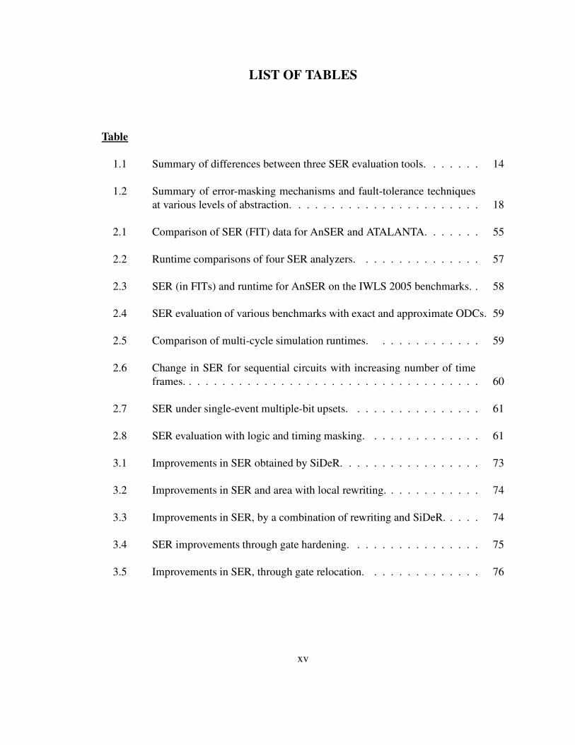
LIST OF TABLES
Table
1.1 Summary of differences between three SER evaluation tools. . . . . . . 14
1.2 Summary of error-masking mechanisms and fault-tolerance techniquesat various levels of abstraction. . . . . . . . . . . . . . . . . . . . . . . 18
2.1 Comparison of SER (FIT) data for AnSER and ATALANTA. . . . . . . 55
2.2 Runtime comparisons of four SER analyzers. . . . . . . . . . . . . . . 57
2.3 SER (in FITs) and runtime for AnSER on the IWLS 2005 benchmarks. . 58
2.4 SER evaluation of various benchmarks with exact and approximate ODCs. 59
2.5 Comparison of multi-cycle simulation runtimes. . . . . . . . . . . . . 59
2.6 Change in SER for sequential circuits with increasing number of timeframes. . . . . . . . . . . . . . . . . . . . . . . . . . . . . . . . . . . . 60
2.7 SER under single-event multiple-bit upsets. . . . . . . . . . . . . . . . 61
2.8 SER evaluation with logic and timing masking. . . . . . . . . . . . . . 61
3.1 Improvements in SER obtained by SiDeR. . . . . . . . . . . . . . . . . 73
3.2 Improvements in SER and area with local rewriting. . . . . . . . . . . . 74
3.3 Improvements in SER, by a combination of rewriting and SiDeR. . . . . 74
3.4 SER improvements through gate hardening. . . . . . . . . . . . . . . . 75
3.5 Improvements in SER, through gate relocation. . . . . . . . . . . . . . 76
xv

4.1 Polynomial approximations of circuit error transfer curves and residualerrors. The fitted polynomials are of the form e(x) ≈ a0 + a1x + a2x2 +a3x3 . . .. . . . . . . . . . . . . . . . . . . . . . . . . . . . . . . . . . . 102
5.1 Statistics on various small benchmarks. . . . . . . . . . . . . . . . . . 111
5.2 Comparison of runtimes and memory usage for levelized ordering andordering computed by dynamic programming. . . . . . . . . . . . . . . 117
6.1 Key differences between deterministic and probabilistic testing. . . . . . 127
6.2 Runtime and memory usage for sensitivity computation for benchmarkcircuits. Faulty gates all have error probability 0.05 for all inputs. . . . . 133
6.3 Number of repetitions required using random vectors versus maximallysensitive test vectors. . . . . . . . . . . . . . . . . . . . . . . . . . . . 138
6.4 Number of test vectors required to detect input signal faults with variousthreshold probabilities pth. Rand is the average number of test vectorsselected during random test generation. . . . . . . . . . . . . . . . . . . 139
xvi
CHAPTER I
Introduction
Digital computers have always been vulnerable to a variety of manufacturing and wear-
out defects. Integrated circuit (IC) chips, which lie at the heart of modern computers,
are subject to silicon-surface imperfections, contaminants, wire shorts, etc. Due to the
prevalence of such defects, various forms of fault tolerance have been built into digital
systems since the 1960s. For example, the first computers NASA sent to space were
equipped with triple-modular redundancy (TMR) [113] to protect their internal logic from
defects.
Over time, IC technology scaling has brought forth heightened device sensitivity to
a different kind of error, known as a soft, or transient, error. Soft errors are caused by
external noise or radiation that temporarily affects circuit behavior without permanently
damaging the hardware. These errors first became problematic in the 1970s, when scien-
tists at Intel noticed that DRAM cells experienced spontaneous bit-flips that could not be
replicated. May and Woods [70] discovered that these errors were a result of α-particles
emitted by trace amounts of radioactive material in ceramic chip packaging. Although the
α-particle problem was eliminated for a period of time by using plastic packaging mate-
1

rial, other sources of soft error soon became apparent. Later that year, Ziegler et al. [130]
at IBM, showed that cosmic rays, consisting primarily of neutrons produced by cosmic
rays from outer space, could also cause errors. The neutrons could strike p-n junctions of
transistors and create enough electron-hole pairs for current to flow through the junctions.
With the advent of nanoscale computing, soft errors are beginning to affect not only
memory but also combinational logic. Unlike errors in memory, errors in combinational
logic cannot be easily corrected and can lead to system failures, with potentially disastrous
results in error-critical systems such as pacemakers, spacecraft, and servers. Additionally,
new device technologies such as carbon nanotubes (CNTs), resonant tunneling diodes
(RTDs), and quantum computers exhibit inherently probabilistic behavior due to nanoscale
and quantum-mechanical effects. Resilience under these sources of uncertainty is vital for
technology and performance improvements.
Due to the cost and high power consumption of modern ICs, the widespread addition
of redundancy is not a practical option for curtailing error rates. Instead, careful circuit
analysis and low-cost methods of improving reliability are necessary. Further, circuits
must be tested post-manufacture for their vulnerability to transient faults as well as to
manufacturing defects.
In the remainder of this chapter, we describe soft errors and technology trends that lead
to increased uncertainty in circuit behavior. We also survey previous work on soft-error
rate (SER) analysis, fault-tolerant design, SER testing, and probabilistic-circuit analysis.
Finally, we state the goals of our research and outline the remaining chapters.
2

1.1 Background and Motivation
Soft errors are one of the main causes of uncertainty and failure in logic circuits [114].
Current trends in circuit technology are exacerbating the frequency and impact of soft
errors. In this section, we describe soft errors and how they affect circuit behavior. We also
survey technology trends, from current CMOS ICs to quantum and molecular computing.
1.1.1 Soft Errors
A soft error is a signal that has an incorrect logic value but does not imply a per-
manent defect. Soft errors can be caused by cosmic rays, α-particles, and even thermal
noise. Cosmic rays are particles that originate in space, usually from supernovas or solar
flares, and enter the Earth’s atmosphere. They are estimated to consist of 92% protons,
6% α-particles, and 2% heavy nuclei [129]. When primary cosmic particles enter the at-
mosphere, they can create a shower of secondary and tertiary particles, as shown in Figure
1.1. Some of these particles can eventually reach the ground and disturb circuit behavior.
While cosmic rays are more problematic at higher altitudes, α-particles can affect cir-
cuits at any altitude. An α-particle (or equivalently, a helium nucleus) consists of two
protons and two neutrons that are bound together. They are emitted by radioactive ele-
ments, such as the uranium or lead isotopes in chip-packaging materials. When packaging
materials were improved in the 1980s, the problem was eliminated to a large extent; how-
ever, as device technologies scale down towards 32nm, the particle energy required to
upset the state of registers and memory circuits becomes smaller [41]. Figure 1.2 shows
that even at 1.25 MeV, incident particles can alter the state of latches, depending on the
angle of incidence. As the energy threshold for causing an error decreases, the number
3

Figure 1.1: Shower of error-inducing particles caused by a primary particle in the atmo-sphere [129].
of particles with sufficient energy to cause errors increases rapidly [106]. For instance,
even the lead in solder balls or trace amounts of radioactive contaminants in tin can affect
CMOS circuits at lower energies [40].
When a particle actually strikes a circuit and lands in the sensitive area of a logic gate,
it can cause an ionized track in silicon, known as a single-event upset (SEU), as illustrated
4

in Figure 1.3. An SEU is a transient, or soft, fault as opposed to a permanent fault. The
effects of an SEU do not propagate if the charge deposited is below the critical charge
Qcrit required to switch the corresponding transistor on or off [114]. If an SEU deposits
enough charge to cause a spurious signal pulse or glitch in the circuit, it produces a soft
error. Error propagation from the site of fault occurrence to a flip-flop or primary output is
stopped if there is no logically sensitized path for the error to pass through. If a soft error
is propagated to and captured or ”latched” by a flip-flop, then it can persist in a system for
several clock cycles.
A single latched error can also fan out to multiple flip-flops. Unlike errors in memory,
errors in combinational logic cannot be rectified using error-correcting codes (ECCs) with-
out incurring significant area overhead. Hence, it becomes vital to find ways to accurately
Figure 1.2: Latch failure for 1.25MeV proton strikes, as a function of the angle of inci-dence [106].
5

Figure 1.3: Ionized track in a transistor, caused by cosmic radiation [34].
analyze and decrease the soft-error rate (SER) of a circuit through careful design. This is
especially true of circuits in mission-critical applications, such as servers and aircraft and
medical devices.
1.1.2 Technology Trends
As described by Moore’s Law in 1965, the number of transistors in an IC tends to
double every two years—a trend that has continued to the present; see Figure 1.4. In
order to facilitate this growth, chip features have become smaller, alongside the amount
of charge stored and transferred between gates during computation. Consequently, the
various sources of uncertainty described in the previous section can disrupt circuit func-
tionality with greater ease. Other technology trends affecting the SER include decreasing
power supply voltage and increasing operating frequency.
The power supply voltage has steadily decreased to improve the power performance of
ICs. Additionally, dynamic voltage scaling is now being employed for further reductions in
power consumption. Keyes and Landauer [47] lower-bound the energy required to switch
a logic gate by KT ln2, where K is the Boltzmann constant and T is the temperature.
6

A more accurate estimate is given by CV 2, where V is the supply voltage and C is the
capacitance of the gate given by C = WCout +∑ f anout CinWj +CL. Here, Cin, Cout , and CL
are the input, output, and load capacitance of the gate, respectively, while W is the width
of the transistor. Therefore, as W and V decrease, the switching energy approaches KT ln2,
causing logic gates to become more susceptible to noise.
Figure 1.4: Moore’s law, showing IC density increase per year.
Increased operating frequency—another technology trend—can lead to designs with
smaller logic depth, i.e., fewer levels of logic gates. This means that fewer errors are
masked by the intermediate gates between the site of fault occurrence and a flip-flop. En-
gineers at IROC Technologies have observed that the SER in logic circuits increases pro-
portionally with operating frequency [44]. Processors with 40MHz operating frequency
were tested, and 400MHz processors were simulated. The results, shown in Figure 1.5,
indicate that at higher frequencies, the SER of logic is only 10 times smaller than the SER
of memories—despite the additional sources of masking present in logic circuits.
7

Figure 1.5: Memory and logic sensitivity to soft errors in the RISC processor [44].
IC technologies beyond CMOS are expected to exhibit even more probabilistic behav-
ior. Examples of new device technologies under active investigation include carbon nan-
otube transistors (CNTs), resonant-tunneling diodes (RTDs), quantum cellular automata
(QCA), and various quantum computing technologies, like ion traps that handle quan-
tum bits (qubits). CNTs and RTDs experience high error probabilities because they oper-
ate near the thermal limit of KT ln2 [69, 14]. QCAs have two main sources of error: 1)
decay—when electrons that store information are lost to the environment, and 2) switching
error—when the electrons do not properly switch from one state to another due to back-
ground noise or voltage fluctuations [62, 104]. Quantum computing devices are inherently
probabilistic (even during fault-free operation) because qubits exist in superposition states
and collapse to either 0 or 1, with different probabilities upon measurement.
Finally, technology scaling also makes devices harder to manufacture. Process vari-
ations cause stochastic behavior, in the sense that device parameters are not accurately
known after manufacture. While most process parameters do not change after manufac-
ture, they can often be modeled probabilistically. Figure 1.6 illustrates the lithography
wavelengths associated with smaller IC feature sizes by year. As the gap between the
8

wavelength and feature sizes continues to widen, it becomes difficult for manufacturers
to control gate and wire widths. Neighboring wires can suffer from crosstalk, the ca-
pacitive and inductive coupling that occurs when two adjacent wires run parallel to each
other. Crosstalk can delay or speed up signal transitions and sometimes causes glitches
that resembles SEUs to appear [96]. Also, as the number of dopant atoms in transistors
decreases, a difference of just a few atoms can lead to large variations in threshold voltage
[15]. These variations can cause inherent uncertainty in circuit behavior.
Figure 1.6: Feature-size trends in ICs by year [34].
1.2 Related Work
In this section, we discuss related work in soft-error rate (SER) analysis, fault-tolerance
techniques, soft-error testing, and probabilistic circuit analysis.
9

1.2.1 Soft-Error Rate Analysis
We first introduce the problem of SER estimation and discuss solutions that appear in
the literature, often alongside our work. The aim here is to reveal the intuition behind SER
analysis methods and to motivate techniques introduced in later chapters.
Figure 1.7: Illustration of transient-fault propagation in combinational logic.
There are several factors to consider in determining the SER of a logic circuit. Figure
1.7 illustrates the three main conditions that are required for an SEU to be latched, and
these conditions are explained below.
• The SEU must have sufficient energy to change a signal and propagate the erroneous
signal value through subsequent gates. If not, the fault is electrically masked.
• The change in a signal’s value must be propagated through the logic to affect a
primary output. If not, the fault is logically masked.
• The fault must reach a flip-flop during the sensitive portion of a clock cycle, nor-
10

mally known as the latching window. If not, the fault is temporally masked.
The probability of electrically masking a fault depends on the electrical characteris-
tics of the gates it encounters on its way to the primary output, i.e., it is path-dependent.
Similarly, the propagation delay of the SEU, before reaching a latch or a primary output,
depends on the gate and interconnect delays along the path it takes. Any path the SEU
takes has to have non-controlling values on side inputs. Therefore, different input vectors
can sensitize different sets of paths.
Assuming a single strike per clock cycle, the SER can be computed using the brute-
force algorithm given in Figure 1.9. In this algorithm, Perr is the probability of an error on
a gate. It is computed using the following variables.
• P(i), the probability of vector i being applied to the input,
• Pstrike(n), the probability of a fault at location n,
• Pattenuate(path(p)), the probability of attenuation along path p, and
• Platch(p,o), the probability of an error arriving on path p at output o during a latching
phase of a clock cycle.
Since the four values are probabilities, neglecting to model any of these factors leads to
overestimation of the SER. Figure 1.8 shows an example of an SEU in the ISCAS-85
circuit C17, along with logically sensitized paths for different input vectors.
The algorithm of Figure 1.9 is only practical for the smallest of circuits. The number
of input vectors to a circuit is exponential in the number of inputs, and the number of
sensitized paths can grow exponentially in the size of the circuit [99]. Therefore, even
11

Figure 1.8: Illustration of logically sensitized paths (in heavy lines) for error propagationwith respect to a specific input vector.
compute SER(circuit C){
for(input vector i)for(node n ∈C)
for(output o ∈C)for(sensitized path p ∈ path(i,n))
Pprop(n) = (1−Pattenuate(p))Perr(C)+ = P(i)Pstrike(n)Pprop(n)Platch(p,o)
return Perr(C)}
Figure 1.9: Basic SER computation algorithm.
determining the probability of logical masking is as difficult as counting the number of
solutions to a SAT instance—a problem in the ]P-hard complexity class.
Several software tools have been recently shown to approximate the SER for com-
binational circuits. Below, we describe three of these tools and their SER computation
techniques [134, 135, 100]. Of the three algorithms, SERA is closest to that of Figure 1.9.
SERA relies on user-specified input patterns and analyzes each input vector individually.
For each gate, SERA finds all the paths from the gate to an output. Then, SEU-induced
12

glitches are simulated on inverter chains of the same lengths as the paths in order to de-
termine the probability of electrical masking. In general, there can be many paths of the
same length, but only one representative inverter chain of each length is simulated. Since
the number of paths is in the size of the circuit, this algorithm runs in exponential time in
the worst case. However, the average runtime is much smaller since SERA only simulates
paths of unique length.
Unlike SERA, FASER [135] uses binary decision diagrams (BDDs) to enumerate all
possible input vectors. A BDD is created for each gate in a circuit—a static BDD for gates
outside the fan-out cone of the glitch location, and duration and amplitude BDDs for gates
in the fan-out cone of the glitch location. Then, these BDDs are merged in topological
order. During the process of merging, the width and amplitude of glitches at inputs are
decreased according to FASER’s estimation of electrical masking. Due to complete input-
vector enumeration, FASER’s BDD representations can require a lot of memory for many
practical circuits, especially multipliers. FASER attempts to lessen the amount of memory
used by partitioning the circuit into smaller subcircuits and then treating the inputs to these
subcircuits as pseudo-primary inputs.
SET’s algorithm [100] proceeds in topological order and considers each gate only once.
For each gate, SET encodes the probability and shape of a glitch as a Weibull probability-
density function. This distribution over the Weibull parameters is known as an SER de-
scriptor (SERD). The SERD for each gate is combined with those of its inputs, to produce
the output SERD. The Weibull parameters are slightly changed at each gate to account for
electrical attenuation, and the new output SERDs are passed on to their successor gates.
13

The SET algorithm is similar to static timing analysis (STA) and does not consider false
paths. The authors of SET do provide another vector-driven mode that computes SER
vector-by-vector to account for input-pattern dependence.
Table 1.1 summarizes the main characteristics of the tools described above, as well as
their methods for incorporating masking mechanisms. These tools have vastly different
methods of computing SER, and their different assumptions can yield very different SER
values for the same circuit.
Attribute SERA FASER SETLogic masking Vector simulation BDD-based analysis Vector simulationTiming masking SER derating No details given SER deratingElectrical masking Inverter-chain simulation Gate characterization Gate characterizationFault assumptions Single Single Multiple
Table 1.1: Summary of differences between three SER evaluation tools.
Our work aims to build SER analysis tools that are scalable and can be used early in
the logic design phase [58, 59, 55]. Due to our emphasis on reliability-driven logic design,
we focus on modeling logical masking both accurately and efficiently. We then use our
tools to guide several design techniques to improve circuit resilience against soft errors.
1.2.2 Fault-Tolerant Design
Techniques for transient-fault tolerance have been developed for use at nearly all stages
of the design flow. Generally, these techniques rely on enhancing masking mechanisms
to mitigate error propagation. Below, we discuss several techniques and highlight their
masking mechanisms.
Faults can be detected at the architectural level via some form of redundancy and can
be corrected by rolling back to a checkpoint to replay instructions from that checkpoint.
14

Redundant multi-threading (RMT) [82, 107] is another common method of error detection
at the architectural level. RMT refers to running multiple threads of the same program and
comparing results. The first thread, known as the leading thread, often executes ahead of
other threads to allow time for transient glitches to dissipate.
The DIVA method [7, 126] advocates the use of a functional checker to augment detect-
and-replay by recomputing results before they are committed. Since the data fetch is
assumed to be error-free (and memory is assumed to be protected by ECC), the functional
checkers simply rerun computations on pre-fetched data. Other methods attempt to detect
errors using symptoms that are unusual behaviors for specific programs. An example
is given by an instruction that accesses data spatially far from previous executions of the
same instruction. Another example is a branch predictor that misspeculates with unusually
high frequency [97, 6]. The main masking mechanism in these techniques is functional
masking. Components are selected for the addition of fault tolerance using a metric called
the architectural vulnerability factor (AVF) of the component in question, as computed by
statistical fault injection or other forms of performance analysis [80].
At the logic level, designers have complete information about the function of the circuit
and its decomposition into gates or other low-level functional modules. At this level, one
can assess logic masking in more detail. Traditionally, logic masking has been increased
by adding gate-level redundancy to the circuit. John von Neumann [125], in his classic
paper on reliability, showed that it is possible to build reliable circuits with unreliable
components, using schemes like cascaded triple modular redundancy (CTMR) and NAND
multiplexing. CTMR contains TMR units that are, in turn, replicated thrice, and this
15

process is repeated until the required reliability is reached.
In NAND multiplexing, each unreliable signal is replicated N times. Then, a set of
NAND gates, each of which takes two of the N redundant signals as inputs, is used as
a simple majority function. Some of these NAND gates may produce incorrect outputs
due to an unfortunate combination of inputs; however, such instances are rare since a
random permutation changes the gate-pairs between stages of multiplexers. von Neumann
concluded that as long as component error probabilities are below a certain threshold,
redundancy can increase the reliability of a system to any required degree.
Techniques that involve replicating an entire circuit increase chip area significantly
and, therefore, decrease chip yield. Mohanram and Touba [76] propose to partially tripli-
cate logic by selecting regions of the circuit that are especially susceptible to soft errors.
Such regions are selected by simulating faults with random test vectors. Dominant-value
reduction [76] is also used to duplicate, rather than triplicate, selected logic. Dominant-
value reduction mitigates the soft errors that cause only one of the erroneous transitions
0-1 or 1-0, depending on which is more common. More recently, Almukhaizim et al. [3]
used a design modification technique, called rewiring, to increase reliability. In the spirit
of [3], our work focuses on lightweight modifications to the circuit that increase reliability
without requiring significant amounts of redundancy. These types of modifications will be
discussed further in Chapter III.
At the transistor level, gates can be electrically characterized, and electrical mask-
ing can be used as an error-mitigation mechanism. Gate sizing is a common technique
for increasing electrical masking: increasing the area of a gate increases its internal ca-
16

pacitance and, therefore, the critical charge Qcrit necessary for a particle strike to alter a
signal. However, this technique increases circuit area and can also increase critical path
delay. Therefore, gates are usually selected for hardening according to their susceptibility
to error, which requires error-susceptibility analysis at the logic level.
Another transistor-level technique for soft-error mitigation is the dual-port design style
proposed by Baze et al. [9] and, later, by Zhang et al. [132]. Dual-port gates, illustrated
in Figure 1.13, decrease charge-collection efficiency, using two extra transistors placed in
a separate well from the original transistors.
In the 1990s, Nicolaidis proposed another method of increasing electrical masking
[87]. In this method, three latches sample a signal with small delays between, and a voter
is used to decide the correct value of the signal. Since stray glitches tend to have short
durations, the erroneous value induced by a glitch is likely to be sampled by only one of
the three latches. Razor [33] uses this idea for dynamic voltage scaling, sampling signals
twice and, when an error is found, restoring program correctness via a detect-and-playback
scheme. The recently-proposed BISER [131] architecture duplicates flip-flops and feeds
the outputs to a C-element and a keeper circuit. At each clock cycle, if the new flip-
flop values are the same, the C-element forwards the new value to the primary outputs;
otherwise, the C-element retains the value from the previous cycle. See Figure 1.14 for the
BISER flip-flop design.
Finally, after the placement and routing of a circuit are completed, gate and intercon-
nect delays can be determined. In earlier IC technology, timing was usually analyzed at
the gate level, since wire delay contributed only a small (often negligible) fraction of the
17

Level Masking mechanism Fault-tolerance techniquesArchitecture/RTL Functional masking Multithreading, functional checkers, replayLogic Logic masking TMR, NAND-mux, partial replication, rewiringTransistor Electrical masking Gate hardening, dual-port gates, dual samplingPhysical Timing masking No known techniques
Table 1.2: Summary of error-masking mechanisms and fault-tolerance techniques at vari-ous levels of abstraction.
critical path delay. However, in current technology, wire delay dominates gate delay and
needs to be incorporated into any accurate timing analyzer. Once we can analyze the tim-
ing, we can also obtain information about timing masking [114, 74]. To date, very few
techniques that decrease timing masking have been proposed.
In summary, faults can be mitigated at several levels of abstraction including the ar-
chitecture, logic, transistor, and physical levels. Solutions at the logic and transistor levels
tend to be more general and do not depend on the function of the circuit. Our work indi-
cates that fine-grained, accurate SER analysis at low levels is computationally feasible and
decreases overhead [58, 59, 55]. Table 1.2 summarizes the fault-tolerance techniques and
masking mechanisms discussed in this section.
1.2.3 Soft-Error Testing
Chip manufacturers including IBM, Intel, and Toshiba, as well as medical equipment
manufacturers like Medtronics, routinely test their chips for SER [129, 70, 50, 127]. SER
testing is normally done in one of two ways: field testing or accelerated testing. In field
testing, a large number of devices are connected to testers and evaluated for several months
under normal operating conditions. In accelerated testing [130], devices are irradiated with
neutron or α-particle beams, thus shortening the test-time to a few hours. Accelerated tests
18

can be further sped up by reducing the power-supply voltage, which changes the Qcrit of
transistors.
There has been some difficulty, however, in translating the SER obtained by acceler-
ated testing to that of field testing [50]. For instance, the SER may vary over time due
to solar activity, which can be difficult to replicate in a laboratory setting. Also, intense
radiation beams can cause multiple simultaneous errors, triggering system failures more
often than normal. Therefore, it is necessary to field-test some devices to calibrate the
accelerated tests.
Since field testing requires a vast number of devices and dedicated testers for each de-
vice, Polian et al.[39] have proposed a non-concurrent built-in self-test (BIST) architecture
for online testing. They define the impact of various soft faults on the circuit in terms of
frequency, observability, and severity. For instance, more frequent and observable faults
are considered more impactful than rare faults. With this fault characterization, integer
linear programming (ILP) is used to generate tests for various objectives, such as ensuring
a minimum fault-detection probability.
Recently, researchers have sought to accelerate testing by selecting test patterns that
sensitize faults. Conceptually, the main difference between testing for hard errors versus
soft errors is that soft errors are only present for a fraction of the test time. Therefore, test
vectors must be repeated to detect faults, and they must be selected to sensitize the most
frequent faults. Sanyal et al. [108] accelerate testing by selecting a set of error-critical
nodes and deriving test sets that, using ILP, sensitize the maximum number of these faults.
In our work, which preceded [108], we developed a way of identifying error-sensitive test
19

vectors for multiple faults, which could include other masking mechanisms like electrical
masking, and we devised algorithms for generating test sets to accelerate SER testing
[54, 53].
1.2.4 Probabilistic Analysis of Circuits
Soft errors and new device technologies are projected to make circuit behavior gener-
ally more uncertain. Therefore, circuit design and testing require new types of probabilistic
analysis that goes beyond soft error analysis only. In this section, we provide background
on the probabilistic analysis of logic circuits, using Bayesian networks and Markov ran-
dom fields.
In our work, we develop a novel probabilistic matrix-based model for gates, and we
use matrix operations and symbolic methods to evaluate overall circuit error probabilities
[60, 61]. More recently, Rejimon et al. [104] proposed capturing errors in nano-domain
logic circuits by Bayesian networks. A Bayesian network is a directed graph with nodes
representing variables and edges representing dependence relations among the variables.
If there is an edge from node a to another node b, then we say that a is a parent of b. If
there are n variables, x1 . . .xn, then the joint-probability distribution for x1 through xn is
represented as the product of the conditional probability distributions
Πni=1P[xi|parents(xi)]
If xi has no parents, its probability distribution is said to be unconditional. In order
to carry out numerical calculations on a Bayesian network, each node xi is labeled with a
probability distribution, conditioned on its parents. The probability distribution of xi can
be given in tabular form or by specifying a known distribution. Certain nodes (such as
20

those corresponding to primary inputs) are given pre-defined probabilities. The probabil-
ities of other nodes are then computed using a method called belief propagation. Joint
probabilities are computed in large Bayesian networks using sampling methods such as
importance sampling. Many tools [35, 89] exist for Bayesian network analysis.
Bahar et al.[14] propose to model and design CNT-based neural networks using Markov
random fields (MRFs). MRFs are similar to Bayesian networks in that they specify joint-
probability distributions in terms of local conditional probabilities, but they can also de-
scribe cyclic dependences. In [14], the neural network is described by an MRF with node
values computed by a weighted sum of conditional probabilities of a neighboring clique
of nodes. This formulation of an MRF is known as the Gibbs formulation and lends itself
to optimizing for clique energy, which is translated into low probabilities of node error in
[14]. Related to this, Nepal et al. [86] present a method for implementing MRF-based
circuits in CMOS, and Bhadhuri et al. [12] describe a software tool, known as Nanolab,
which uses the algorithm from [14] to automate the design of fault-tolerant architectures,
like CTMR, in nanotechnologies.
1.3 Thesis Outline
In this dissertation, we focus on gate-level SER analysis, probabilistic circuit analysis,
and fault-tolerant design. We carefully study the input-vector dependence in logic, as well
as timing masking, in order to design circuits with better reliability. We further develop
methods to model inherently probabilistic methods in logic circuits and to test circuits for
determining their reliability after they are manufactured. Our main goals are:
• To develop scalable and accurate methods of SER and susceptibility analysis, usable
21

during the CAD flow at the gate level,
• To devise methods that guide logic design towards greater resilience against soft
errors,
• To develop general and accurate methods for modeling and reasoning about proba-
bilistic behavior in logic circuits, and
• To develop test methods for accurately and efficiently measuring soft-error suscep-
tibility in circuits after they are manufactured.
The remainder of this dissertation is organized as follows. Chapter II presents an ef-
ficient technique to analyze SER at the logic level. Here, we formulate probabilistic fault
models, based on the stuck-at model used in the testing literature. We propose ways to
account for the three basic masking mechanisms, using probabilistic reasoning and func-
tional simulation. We also present techniques in the spirit of static-timing analysis to
estimate timing masking and use derating factors to account for electrical masking. Our
analysis methods are also extended to sequential circuits.
In Chapter III, we apply the analysis techniques from the previous chapter to the design
of reliable circuits. Our techniques include logic rewriting, gate hardening, and a novel
technique we call SiDeR. This technique uses functional relationships between signals
to partially replicate areas of logic with low redundancy. We also present a gate reloca-
tion technique that targets timing masking, a factor which has often been overlooked in
fault-tolerant design. This technique entails no area overhead and negligible performance
overhead. For sequential circuits, we derive integer linear programs for retiming, which
22

move latches to positions where they are less likely to propagate errors to primary outputs.
Chapter IV presents a general matrix-based reliability analysis technique, the proba-
bilistic transfer matrix (PTM) framework, to model faulty gate behavior. PTMs form an
algebra for reasoning about uncertain behavior in logic circuits. The algebra includes sev-
eral specific types of matrices to describe gates and wires, along with matrix operations
that can be used symbolically or numerically to combine the matrices. Several new ma-
trix operations that are useful in modifying and combining PTMs are introduced to derive
information about circuit reliability and output error probabilities, under various types of
faults.
Chapter V develops decision diagram-based methods for compressing and computing
with PTMs. Several heuristics are presented for improving the scalability of PTM-based
computations, including dynamic evaluation ordering, partitioning, hierarchical computa-
tion, and sampling.
Chapter VI introduces a new method to test for probabilistic faults. We discuss the
differences among traditional testing methods geared towards identifying structural defects
and assessing circuit susceptibility to probabilistic faults. We also present algorithms for
compacting the test-vector set.
Finally, Chapter VII summarizes our work and discusses possible directions for future
research.
23

compute SER SERA(circuit C, vectors V)
{for(v ∈V)
for(nodes n ∈C)for(output o ∈C)
for(sensitized path p ∈ path(n,v))l = length(p)Perr(n) = simulate inverter chain(l)K = Area(n)/Area(C)Perr(C)+ = Perr(n)∗K
return Perr(C)}
(a)
compute SER FASER(circuit C){
for(n ∈C)create strike BDD(n)for(output o ∈C)
for(gate g ∈Ccreate static BDD(g)if(g ∈ f anout(n))modify terminals(g)
sort topological(C)for(g ∈C)attenuate(inputs(g))merge BDD(inputs(g))
Perr(C)+ = (Area(n)/Total)∗Flux∗Perr(BDD(o))return Perr(C)
}(b)
compute SER SET(circuit C){sort topological(C)for(gate g ∈ G)
SERD(g) = calculate strike SERD(g)SERD(g) = merge input SERD(SERD(g),inputs(g))
for(output o ∈ C)
Perr(C)+ = Perr(SERD(o))return Perr(C)
}(c)
Figure 1.10: Algorithms for SER computation used by (a) SERA, (b) FASER, and (c) SET.
24

1
2
3
4
5
6
7
8
9
1
2
3
Figure 1.11: The cascaded TMR scheme; M denotes a Majority gate [125].
Majority
Rand
omPe
rmut
atio
n
Rand
omPe
rmut
atio
n
Maj
ority
Gat
eM
Figure 1.12: The NAND-multiplexing scheme [125].
25

(a) (b)
Figure 1.13: (a) Normal and (b) dual-port CMOS inverter with two additional transistorsin an isolated well [9].
Figure 1.14: The error-correcting BISER flip-flop design with a C-element and a keepercircuit [131].
26

CHAPTER II
Signature-based Soft-error Analysis
As soft errors become increasingly prevalent in logic circuits, soft-error rate (SER)
prediction becomes important in all phases of design. As discussed in Section 1.2, the SER
depends not only on noise effects, but also on the logical, electrical, and timing-masking
characteristics of the circuit. Each of these types of masking can be predicted with a fair
amount of accuracy after certain phases of the design process—logic masking after logic
design, electrical masking after technology mapping, and timing masking after physical
design—and generally stays in effect through the rest of the design flow. Therefore, it is
important to efficiently and accurately analyze the SER during the actual design process.
This chapter presents the SER analyzer called AnSER. AnSER employs functional-
simulation signatures extensively in order to estimate logic masking and to account for the
input-vector dependence in timing and electrical masking. Signatures provide an efficient
way of computing testability measures like signal probability and observability, which
are, in turn, closely connected to the probability of error propagation. More specifically,
the probability of logic-fault propagation is the same as the testability of the fault. The
testability of a fault is the likelihood of a test vector for the fault being applied at the
27

primary inputs. Enumerating test vectors for a particular fault is known to be a problem
with ]P-hard complexity. In other words, it has the same complexity as counting the
number of solutions to a SAT instance. Since exact analysis is impractical for all but
the smallest of circuits, we estimate testability using a new and efficient signature-based
algorithm.
Figure 2.1 illustrates the flow of computation in AnSER. Functional-simulation signa-
tures are computed from logical information, error-derating factors from gate-characterization
information, and error-latching windows from static-timing analysis. These smaller com-
putations are combined to form an estimate of circuit SER. Since AnSER is intended to be
used alongside logical and physical design tools, we pay particular attention to runtime,
memory requirements and the incremental-use model. Figure 2.1 also shows how AnSER
can be incorporated into a typical RTL-to-GDSII flow through incremental calls after each
change to the netlist or placement.
The remainder of this chapter is organized as follows. Section 2.1 develops our method
for computing the SER of logic circuits by accounting for logic masking. Section 2.2 ex-
tends this methodology to sequential circuits. Finally, Section 2.3 incorporates timing and
electrical masking into our SER estimates. Most of the techniques and results presented in
this chapter also appear in [58, 55, 59, 57].
2.1 SER in Combinational Logic
In this section, we present an SER analysis method for combinational logic which,
by definition, contains no memory. We first develop fault models for soft errors. Then,
we provide background on functional-simulation signatures, which we use extensively in
28

Timing Masking Latching-window
computations
SER Algorithms
Reliability-Guided Design
Timing Analyzer
Electrical Masking Derating Factors
FunctionalSimulation
SignaturesODC masks
ElectricalCharacterization
Design ToolsSynthesis
Physical Design
Circuit DataNetlist
PlacementCell Library Bindings
Figure 2.1: Computational flow of AnSER.
AnSER. Next, we derive SER algorithms for single- and multiple-fault assumptions using
signal probability and observability measures that are computed using signatures. Finally,
we show how to account for electrical and timing masking.
2.1.1 Fault Models for Soft Errors
For the purposes of logic-level reasoning, we formulate a model for single transient
faults with extensions to account for multiple faults. In general, fault models are abstract,
logic-level representations of defects and are usually employed in automatic test-pattern
generation (ATPG) algorithms. Fault models for soft errors, as we show in Chapter VI,
can be useful for testing. However, in this section their primary use is in SER analysis; the
close connections between testability and SER facilitate this use.
We conceptualize external noise (such as an SEU) as a probabilistic fault. The main
29

difference between a permanent fault and a transient fault is its persistence, which we
model as a probability of error per clock cycle. Each circuit node g can potentially ex-
perience a temporary single stuck-at-1 (TSA-1) fault with probability a Perr1(g), and a
temporary single stuck-at-0 (TSA-0) fault with probability Perr0(g).
Definition 1 A transient stuck-at (TSA) fault is a triple, (g,v,Perr(g)) where g is a node
in the circuit, v ∈ {0,1} indicates a stuck-at value, and Perr(g) is the probability of a
stuck-at fault when the node has correct value v.
The advantage of basing a fault model on the stuck-at model is that test vectors for
TSA faults can be derived in the same way as for SA faults. Therefore, the same ATPG
tools can be used for TSA faults as well. The TSA fault model, in particular, assumes that
at most one fault will occur in any clock cycle. This assumption is common in much of
SER research because for most technologies, the intrinsic error rate (due to neutron flux,
for instance) is fairly low. Using the single-error assumption, SER can be computed as the
sum of gate/component contributions. The contribution of each gate to the SER depends
on the SEU rate of the particular gate, as captured by Perr(g), and on the observability of
the error.
In the case of multiple faults, we have to consider the possible sets of gates that experi-
ence faults in the same cycle and the possibility that these faults interfere with each other.
The TSA model can be extended to two types of multiple faults called transient multiple
correlated stuck-at faults, and transient multiple stuck-at faults.
Faults are correlated if the occurrence of one fault changes the probability of another
fault. An example is a multiple-bit upset where a single particle strike causes multiple
30
upsets in nearby gates. Such upsets are spatially correlated.
Definition 2 A transient multiple-correlated stuck-at fault (TMCSA) is the triple (G,V,Perr)
where G is a set of node {g1,g2,g3, . . .}, V is a set of binary values {v1,v2,v3 . . .vn} that
correspond to the stuck-at values of nodes in G, and Perr is the joint-fault probability of
nodes in G.
Transient multiple stuck-at faults apply to circuits with independent probabilities of
gate or node failure.
Definition 3 A transient multiple stuck-at fault (TMSA) fault is represented by (G,V,P)
where G is a set of nodes {g1,g2, . . .gn}, V is the set of corresponding binary stuck-at
values {v1,v2, . . .vn} and P is the corresponding vector of independent error probabilities
{p1, p2, . . . pn}.
Unlike TSA and TMSA faults, a circuit may contain only one TMSA fault of interest—
the fault with G containing all the nodes in the circuit. TMSA faults may be used to model
independent device failure probabilities rather than SEU effects.
In the next two sections, we mainly utilize the TSA fault model to compute the SER of
logic circuits. It is sometimes convenient to measure the SER in terms of the probability
of error per cycle. The results can easily be converted into units of FIT, or failures per 109
seconds. If the soft-error probability per cycle is p, then the expected number of failures
per 109 seconds is simply p× f req× 109, where f req is the clock frequency. Assuming
only one error occurs in each cycle, Perr0(g) is the probability that only gate g experiences
an error. Therefore, gate SER in units of FITs can also be used in a similar fashion. In
general, we denote probabilities of error Perr and gate SER as gerr.
31

2.1.2 Signatures and Observability Don’t-Cares
We systematically use node signatures for three purposes: 1) to compute the SER, 2) to
identify error-sensitive areas of a circuit, and 3) to identify redundant nodes for resynthesis.
A circuit node g can be labeled by a signature as defined below.
Definition 4 A signature, denoted, sig(g) = Fg(X1)Fg(X2) . . .Fg(XK) is the sequence of
logic values observed at circuit node g in response to applying a sequence of K input
vectors X1,X2, . . . ,XK to the circuit.
Here, Fg(Xi)∈ {0,1} indicates the value appearing at g in response to Xi. The signature
sig(g) thus partially specifies the Boolean function Fg realized by g. Applying all possible
input vectors (exhaustive simulation) generates a signature that corresponds to a full truth
table. In general, sig(g) can be seen as a kind of “supersignal” appearing on g. It is
composed of individual binary signals that are defined by some current set of vectors.
Like the individual signals, sig(g) can be processed by EDA tools such as simulators and
synthesizers as a single entity. It can be propagated through a sequence of logic gates
and combined with other signatures via Boolean operations. This processing can take
advantage of bitwise operations available in CPUs to speed up the overall computation
compared to processing the signals that compose sig(g) one at a time.
Signatures with thousands of bits can be useful in pruning non-equivalent nodes during
equivalence checking [137, 92]. A related speedup technique is also the basis for “parallel”
fault simulation [19]. The basic algorithm for computing signatures is shown for reference
in Figure 2.2. Here, Op < g > refers to the operation gate g. This operation is applied to
the signatures of the input nodes of gate g, denoted inputsigs(g).
32

compute sigs(Circuit C, size K)
{for(all inputs i ∈C)
sig(i) = gen random sig(K)
sort topological(C)for(all nodes g ∈C)
sig(g) = Op < g > (inputsigs(g))}
Figure 2.2: Basic algorithm for signature computation.
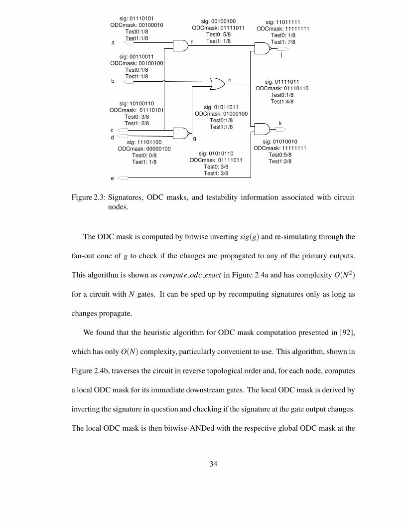
Figure 2.3 shows a 5-input circuit where each of the 10 nodes is labeled by an 8-bit
signature computed with eight input vectors. These vectors are randomly generated, and
conventional functional simulation propagates signatures to the internal and output nodes.
In a typical implementation such as ours, signatures are stored as logical words and ma-
nipulated with 64-bit logical operations, ensuring high simulation throughput. Therefore
64 vector simulations are conducted in parallel with each signature processed. Generating
K-bit signatures in an N-node circuit takes O(NK) time.
Observability don’t-cares (ODCs) occur at a node g for input vectors for which the
value at g does not affect the primary outputs. For example, in the circuit AND(a,OR(a,b)),
the output of the OR gate is inconsequential when a = 0. Hence, input vectors 00 and 01
are ODCs for b.
Definition 5 Corresponding to the K-bit signature sig(g), the ODC mask of g, denoted
ODCmask(g), is the K-bit sequence whose ith bit is 0 if input vector Xi is in the don’t-care
set of g; otherwise the ith bit is 1, i.e., ODCmask(g) = X1 6∈ODC(Fg)X2 6∈ODC(Fg) . . .XK 6∈
ODC(Fg).
33
f
g
h
j
k
b
d
e
a
c
sig: 01110101ODCmask: 00100010
Test0:1/8Test1:1/8
sig: 00110011ODCmask: 00100100
Test0:1/8Test1:1/8
sig: 10100110ODCmask: 01110101
Test0: 3/8Test1: 2/8
sig: 11101100ODCmask: 00000100
Test0: 0/8Test1: 1/8
sig: 01010110ODCmask: 01111011
Test0: 3/8Test1: 3/8
sig: 00100100ODCmask: 01111011
Test0: 5/8Test1: 1/8
sig: 01011011ODCmask: 01000100
Test0:1/8Test1:1/8
sig: 01111011ODCmask: 01110110
Test0:1/8Test1:4/8
sig: 11011111ODCmask: 11111111
Test0: 1/8Test1: 7/8
sig: 01010010ODCmask: 11111111
Test0:5/8Test1:3/8
Figure 2.3: Signatures, ODC masks, and testability information associated with circuitnodes.
The ODC mask is computed by bitwise inverting sig(g) and re-simulating through the
fan-out cone of g to check if the changes are propagated to any of the primary outputs.
This algorithm is shown as compute odc exact in Figure 2.4a and has complexity O(N2)
for a circuit with N gates. It can be sped up by recomputing signatures only as long as
changes propagate.
We found that the heuristic algorithm for ODC mask computation presented in [92],
which has only O(N) complexity, particularly convenient to use. This algorithm, shown in
Figure 2.4b, traverses the circuit in reverse topological order and, for each node, computes
a local ODC mask for its immediate downstream gates. The local ODC mask is derived by
inverting the signature in question and checking if the signature at the gate output changes.
The local ODC mask is then bitwise-ANDed with the respective global ODC mask at the
34

compute odc exact(Circuit C, size K)
{compute sigs(C,K)
sort reverse topological(C)for(all nodes g ∈C)
newsig(g) =∼ sig(g)recompute sigs(C,K,g)for(each output o ∈C)
ODCmask(g)| = newsig(o)⊕ sig(o)restore computed sigs(C)
}(a)
compute odc approx(Circuit C, size K)
{compute sigs(C,K)
sort reverse topological(C)for(all nodes g ∈C)
newsig(g) =∼ sig(g)for(each fan-out branch f ∈ f anout(g))
sig( f ) = Op < f > (inputsigs( f ))localodc(g, f ) = newsig( f )⊕ sig( f )globalodc(g, f ) = localodc(g, f )&ODCmask( f )ODCmask(g)| = globalodc(g, f )
}(b)
Figure 2.4: (a) Exact and (b) approximate ODC mask computation algorithms.
output of the gate to produce the ODC mask of the gate for a particular fan-out branch.
The ODC masks for all fan-out branches are then ORed to produce the final ODC mask
for the node. The ORing takes into account the fact that a node is observable for an input
vector if it is observable along any of its fan-out branches. Reconvergent fan-out can
eventually lead to incorrect values. The masks can then be corrected by performing exact
simulation downstream from the converging nodes. This step is not strictly necessary for
SER evaluation as we show later.
Example 1 Figure 2.3 shows a sample 8-bit signature and the accompanying ODC mask
35

for each node of a 10-node circuit. The ODC mask at c, for instance, is derived by com-
puting ODC masks for paths through nodes f and g, respectively, and then ORing the two.
The local ODC mask of c for the gate through f is 01110101. When this is ANDed with
the ODC mask of f , we find the global ODC mask 01110001 of c on paths through f .
Similarly, the local ODC mask of c for the gate with output g is 11101100, and the global
ODC mask for paths through g is 01000100. We get the ODC mask of c by ORing the
ODC masks for paths through f and g, which yields 01110101.
2.1.3 SER Evaluation
We compute the SER by counting the number of test vectors that propagate the effects
of a transient fault to the output(s). Test-vector counting was also used in [39] to com-
pute SER, although the algorithm there uses BDD-based techniques. Intuitively, if a large
number of test vectors are applied at the inputs, then faults are propagated to the outputs
often. SER computation is inherently more difficult than test generation. Testing involves
generating vectors that sensitize the error signal on a node and propagate the signal’s value
to the output. SER evaluation involves counting the number of vectors that detect faults
on a signal.
Next, we describe how to compute signatures and ODC masks to derive several met-
rics that are necessary for our SER computation algorithm. These metrics are based on
the signal probability (controllability), observability and testability parameters commonly
used in ATPG [19].
Figure 2.5 summarizes our algorithm for SER computation. It involves two topolog-
ical traversals of the target circuit: one to propagate signatures forward and another to
36

compute TSA SER(Circuit C, int K)
{compute sigs(C,K)
compute odc approx(C,K)
for(all nodes g ∈C)test0(g) = zeros(sig(g)&ODCmask(g))/Ktest1(g) = ones(∼ sig(g)&ODCmask(g))/KPerr(C)+ = Perr0(g)test1(g)Perr(C)+ = Perr1(g)test0(g)
return Perr(C)}
Figure 2.5: Algorithm to compute SER under the TSA fault model.
propagate ODC masks backwards. The fraction of 1s in a node’s signature is an estimate
of its signal probability, while the relative proportion of 1s in an ODC mask indicates ob-
servability. These two measures are combined to obtain a testability figure-of-merit for
each node of interest, which is then multiplied by the probability of the associated TSA to
obtain the SER for the node. This SER for the node captures the probability that an error
occurs at the node, combined with the probability that the error is logically propagated
to the output. Our estimate can be contrasted with technology-dependent SER estimates,
which include timing and electrical masking.
We estimate the probability of signal g having logic value 1, denoted P[g = 1], by the
fraction of 1s in the signature sig(g). This is sometimes called the controllability of the
signal.
Definition 6 The controllability of a signal g, denoted P[g = 1], is the probability that g
has logic value 1.
P[g = 1] = ones(sig(g)
)/K(2.1)
37

Definition 7 The observability of a signal g, denoted P[obs(g)] is the probability that a
change in the signals value changes the value of a primary output.
The observability of a node is approximated by the number of 1s in its ODC mask.
P[obs(g)] = ones(ODCmask(g)
)/K(2.2)
This observability metric is an estimate of the probability that g’s value is propagated
to a primary output. The 1-testability of g, denoted P[test1(g)] = P[obs(g),g = 1], is the
number of bit positions where g’s ODC mask and signature both are 1.
Definition 8 The 1-testability of a node g is the probability that the node’s correct value
is 1 and that it is observable.
P[test1(g)] = ones(sig(g)&ODCmask(g)
)/K(2.3)
Similarly, 0-testability is the number of positions where the ODC mask is 1 and the signa-
ture is 0. In other words, 0-testability is an estimate of the number of vectors that test for
stuck-at-0 faults.
Example 2 Consider again the circuit in Figure 2.3. The signature for node g is given
by sig(g) = 01011011 and ODC mask ODCmask(g) = 01000100. Hence, P[g = 1] =
ones(sig(g)) = 5/8, P[g = 0] = 3/8, P[obs(g)] = 2/8, P[test0(g)] = 1/8 and P[test1(g)] =
1/8.
Suppose each node g in a circuit C has fault probabilities Perr0(g) and Perr1(g) for
TSA-0 and TSA-1 faults, respectively, then the SER of C is the sum of SER contributions
38

from each gate g in the circuit. Here, we weight gate error probabilities by the testability
of the gate for the particular TSA.
Perr(C) = ∑g∈C
P[test1(g)]Perr0(g)+P[test0(g)]Perr1(g)(2.4)
Example 3 The test0 and test1 measures for each gate in the circuit are given in Figure
2.3. If each gate has TSA-1 probability Perr0 = p and TSA-0 probability Perr1 = q, then
the SER is given by Perr(C) = 2p+(13/8)q.
The metrics test0 and test1 implicitly incorporate error sensitization and propagation
conditions. Hence, Equation 2.4 accounts for the possibility of an error being logically
masked. Note that the Perr1(g) refers to the 1-controllability of g and so is weighted by
the 0-testability, similarly for Perr1(g).
2.1.4 Multiple-Fault Analysis
In this section, we discuss SER computation for the two multiple-fault models intro-
duced previously: the TMSCA model for multiple correlated faults, and the TMSA model
for multiple independent faults.
The SER for TSA faults requires the computation of signatures and ODC masks for
each node in the circuit. Each node represents the location of a potential TSA fault, and the
ODC mask for each node contains information about the probability of the corresponding
fault being observed. The same process can be generally followed for TMSCA faults.
However, ODC masks must be applied to a set of nodes rather than a single node.
Recall that exact ODC computation of Figure 2.4a requires resimulation of the entire
fan-out cone of the fault location, while the algorithm from [92], shown in Figure 2.4b,
39

only resimulates through the immediate successor gate(s). These techniques represent
two extremes in error-propagation analysis. Between these extremes, it is possible to
resimulate the fan-out cone partially. In fact, the farther through the fan-out cone we
resimulate, the more accurate our ODC masks become. For TMSCA faults, we resimulate
through the subcircuit consisting of gates in the set G. We then bitwise invert the signatures
of all the nodes in the subcircuit and resimulate to either the boundary of the subcircuit
(for approximate ODC computation) or through the entire fan-out cone of the subcircuit
(for exact ODC computation). This algorithm is shown in Figure 2.6. In this algorithm,
the nodes in the set G are topologically sorted and resimulated by flipping the signature of
each node sig(g), to the value V [g]. This requires the use of a bit mask called valsig(g)
that contains V [g] in every bit position. After the resimulation is completed through G,
we check for differences that are propagated to the immediate outputs of G (locally) and
combine them with the global ODCs computed at the outputs of G using the bitwise AND
operation.
For TMSA faults, each of the gates in G has an independent probability of error. Thus,
the difference between computing SER for TMSCA faults and TMSA faults is that the sig-
natures of nodes within G are flipped with independent probabilities. In order to represent
this situation, we only flip a fraction of the bits in each signature randomly. The rest of
the algorithm remains the same. Since usually a single TMSA fault is of interest, we can
compute the exact error propagation probability of a TMSA fault by resimulating through
the entire circuit in only linear time. The algorithm for SER computation using a TMSA
fault is given in Figure 2.7. Here, the circuit is resimulated by selectively flipping the bits
40

in the signatures of gates in G. The bits are flipped randomly based on the probability of
error P[g] and the value V [g] for each node G. The resimulation is done all the way to the
primary outputs , then the primary outputs are checked for any differences that have been
propagated.
compute TMCSA SER(Circuit C, nodes G, values V, Perr P){
T = sort topological(G)
T ′ = find output nodes(Tfor(each node g ∈ T ′)
compute sig(g)if(g ∈ T)
valsig(g) = create sig(V [g])for(each node g ∈ out put(T ′))
di f f (g) = sig(g)⊕newsig(g)ODCmask(G)|= (di f f (g)&ODCmask(g))
return Perr×ones(ODCmask(G))/K}
Figure 2.6: Algorithm to compute SER under the TMCSA fault model.
compute TMSA SER(Circuit C, nodes G, values V, errors P){
sort topological(C)for(each node g ∈C)compute sig(g)if(g ∈ G)
flip sig bits(g,V [g],P[g])for(each node o ∈ out put(C))
di f f (o) = sig(o)⊕newsig(o)ODCmask(G)|= di f f (g)
return Perr×ones(ODCmask(G))/K}
Figure 2.7: Algorithm to compute SER under the TMSA fault model.
In practice, random bits of the signature can be bitwise XORed by a mask with p/K
ones where p is the probability of error. Such a mask can be created by forming a bit
41
vector with p/K ones that are permuted randomly. Then, when the signature is bitwise
XORed with the mask, p/K of the bits are flipped, corresponding to a fault that occurs
with probability p.
2.2 SER Analysis in Sequential Logic
In this section, we extend our SER analysis to handle sequential circuits, which have
memory elements (D flip-flops) in addition to primary inputs and outputs. Recall that the
values stored in the flip-flops collectively form the state of the circuit. The combinational
logic computes state information and primary outputs as a function of the current state and
primary inputs. Below, we list three factors to consider while analyzing sequential-circuit
reliability.
1. Steady-state probability distribution: It has been shown that under normal operation
most sequential circuits converge to particular state distributions [36]. Discovering
the steady-state probability is useful for accurately computing the SER.
2. State reachability: Some states cannot be reached from a given initial state, therefore
only the reachable part of the state space should account for the SER.
3. Sequential observability: Errors in sequential circuits can persist past a single cycle
if captured by a flip-flop. A single error may be captured by multiple flip-flops and
result in a multiple-bit error in subsequent cycles. Such errors can then be masked
by logic.
The following two subsections develop a simulation-based framework to address these
issues.
42

2.2.1 Steady-State and Reachability Analysis
Usually, the primary input distribution is assumed to be uniform, or is explicitly given
by the user, while the state distribution has to be derived. A finite state machine (FSM) is
periodic if its states can be visited only at regular intervals, and, otherwise, is aperiodic.
Periodic FSMs do not reach steady state. Hachtel et al. [36, 23] show that aperiodic
FSMs with strongly-connected state spaces eventually reach a steady-state distribution. A
modulo-d counter is an example of such an FSM. In [23], it is shown that most ISCAS
and other benchmark circuits reach steady-state because they are synchronizable; in other
words, they can be taken to a reset state starting from any state, using a specific fixed-length
input sequence. This indicates that the circuits are aperiodic (otherwise, different-length
sequences would have to be used from each state) and strongly connected (otherwise some
states could not be taken to the reset state).
In order to approximate the steady-state distribution, we perform sequential simulation,
using signatures. Assume that a circuit with m flip-flops L = {l1, l2 . . . lm} is in state SL =
{s0,s1,s2 . . .sm}, where each si ∈ {0,1}. Our method starts in state S0 for each simulation
run (sets of 64 states are processed in parallel in our implementation). Then, we simulate
the circuit for n cycles. Each cycle propagates signatures through the combinational logic
and stops when flip-flops are reached. Primary input values are generated randomly from
a given fixed probability distribution. At the end of each simulation cycle, flip-flop inputs
are transferred to flip-flop outputs, which are, in turn, fed into combinational logic for the
subsequent cycle. All other intermediate signatures are erased before the next simulation
cycle starts. The K-bit signatures of the flip-flops, at the end of n simulations cycles, define
43

K states. We claim that for a large enough n, these states are sampled from the steady-state
probability distribution. Empirical results suggest that most ISCAS benchmarks reach
steady-state in 10 cycles or fewer, under the above operating conditions [75].
Additionally, our signature-based SER analysis methods can handle systems that are
decomposable. Such systems pass through some transient states and are then confined to
a set of strongly connected closed (SCC) states. That is, the system can be partitioned
into transient states and sets of SCC states. For such systems, the steady-state distribution
strongly depends on the initial states. We address this implicitly by performing reachability
analysis starting in a reset state. Thus, each bit of the signature corresponds to a simulation
that 1) starts from a reset state and propagates through the combinational logic, 2) moves
to adjacent reachable states, and 3) for a large enough n, reaches steady-state within the
partition.
Figure 2.8 summarizes our simulation algorithm for sequential circuits. Using this al-
gorithm, simulating a circuit with g gates for n simulation cycles and with K-bit signatures
takes time O(Kng). Note that it does not require matrix-based analysis, which is often the
bottleneck in other methods [36, 75]. For example, Markov matrices are used to encode
state-transition probabilities explicitly, and therefore, can be large due to the problem of
state-space explosion [36, 75].
Figure 2.9 shows an example of sequential simulation with 3-bit signatures. The flip-
flops with outputs x and y are initialized to 000 in cycle 0, T0. Then the combinational
logic is simulated. For cycle T1, the input of x and y are transferred to the output, and the
process continues. At the conclusion of the simulation, the values for x and y at T3 are
44

simulate sequential(Circuit C, int K)
{for(all flip-flops l ∈C)
out putsig(l) = inputsig(l)for(all inputs in0 ∈C)
in0 = new random input()
compute sigs(C,K)
}
Figure 2.8: Algorithm for multi-cycle sequential-circuit simulation.
saved for sequential-error analysis, which is explained in the next subsection.
Q
QSET
CLR
D
Q
QSET
CLR
D
T0: 000T1: 111T2: 001
T0: 000T1: 000T2: 111
T0: 101T1: 110T2: 001
T0: 110T1: 111T2: 101 T0: 110
T1: 111T2: 100
T0: 000T1: 110T2: 001
T0: 111T1: 001T2: 110
T0: 000T1: 111T2: 110
T0: 000T1: 000T2: 001
Figure 2.9: Illustration of bit-parallel sequential simulation.
Although we only considered aperiodic systems, we observe that for a periodic system
the SER would need to be analyzed for the maximum period D, since the state distribution
oscillates over that period. If the FSM is periodic with period D, then we can average over
the SER for D or more simulation cycles.
2.2.2 Error Persistence and Sequential Observability
In order to assess the impact of soft faults on sequential circuits, we analyze several
cycles through which faults persist, using time-frame expansion. This involves making n
45
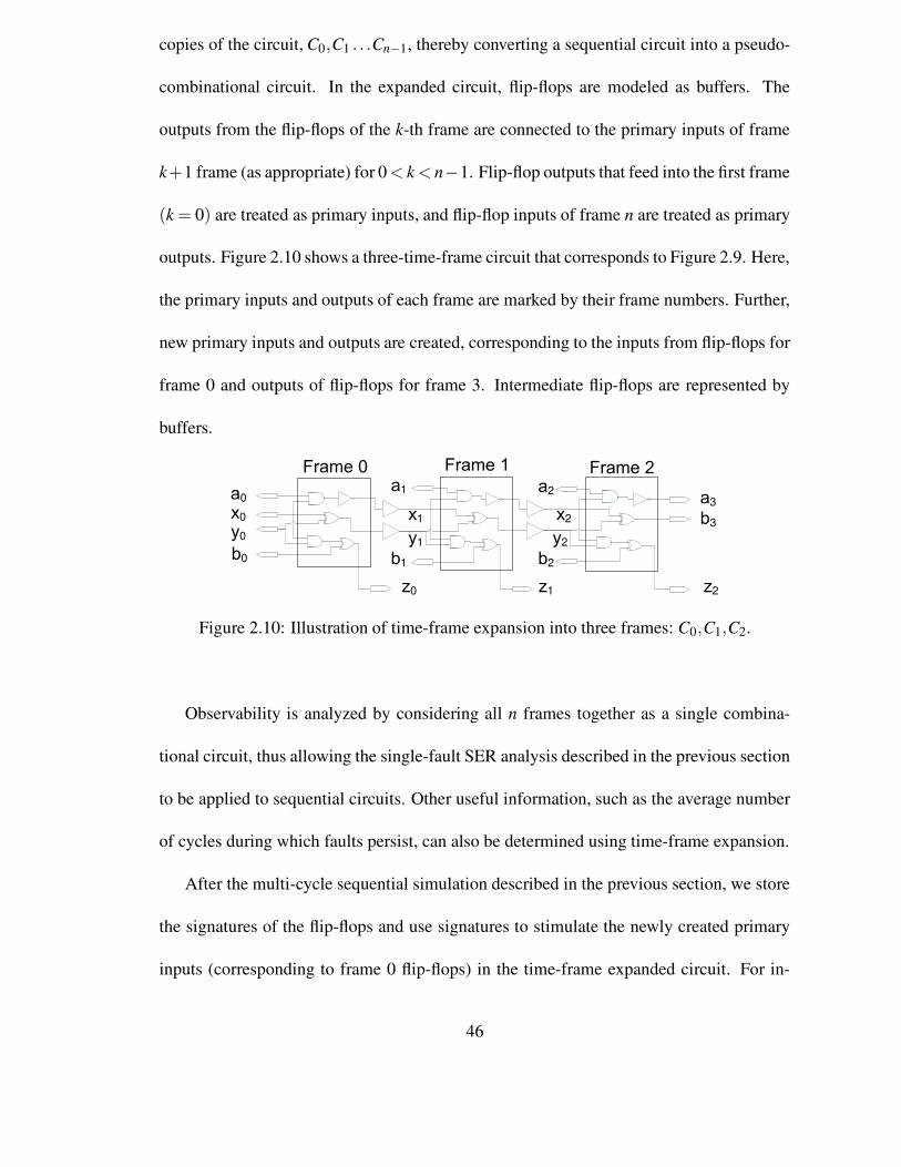
copies of the circuit, C0,C1 . . .Cn−1, thereby converting a sequential circuit into a pseudo-
combinational circuit. In the expanded circuit, flip-flops are modeled as buffers. The
outputs from the flip-flops of the k-th frame are connected to the primary inputs of frame
k+1 frame (as appropriate) for 0 < k < n−1. Flip-flop outputs that feed into the first frame
(k = 0) are treated as primary inputs, and flip-flop inputs of frame n are treated as primary
outputs. Figure 2.10 shows a three-time-frame circuit that corresponds to Figure 2.9. Here,
the primary inputs and outputs of each frame are marked by their frame numbers. Further,
new primary inputs and outputs are created, corresponding to the inputs from flip-flops for
frame 0 and outputs of flip-flops for frame 3. Intermediate flip-flops are represented by
buffers.
000
0
0
1
1
11
1
22
2
2
33
2
Figure 2.10: Illustration of time-frame expansion into three frames: C0,C1,C2.
Observability is analyzed by considering all n frames together as a single combina-
tional circuit, thus allowing the single-fault SER analysis described in the previous section
to be applied to sequential circuits. Other useful information, such as the average number
of cycles during which faults persist, can also be determined using time-frame expansion.
After the multi-cycle sequential simulation described in the previous section, we store
the signatures of the flip-flops and use signatures to stimulate the newly created primary
inputs (corresponding to frame 0 flip-flops) in the time-frame expanded circuit. For in-
46

stance, the x0 and y0 inputs of the circuit in Figure 2.10 are simulated with the correspond-
ing signatures, marked T3 (the final signature after multi-cycle simulation is finished), from
Figure 2.9. Randomly generated signatures are used for primary inputs not corresponding
to flip-flops (such as a0 and b0 in Figure 2.10).
After simulation, we perform ODC analysis, starting from the primary outputs and
flip-flop inputs of the n-th frame and moving all the way to the inputs of the 0-th frame.
In other words, errors in primary outputs and flip-flops are considered to be observable.
Figure 2.11 gives our algorithm for sequential SER computation. The value of n can
be varied until the SER stabilizes, i.e., it does not change appreciably from an n-frame
analysis to an (n+1)-frame analysis.
The n-frame ODC-analysis can lead to different gates being seen as critical for SER.
For instance, the designer can deem errors that persist longer than n cycles as more critical
than errors that are quickly flushed at primary outputs. In this case, the ODC analysis only
considers the fan-in cones of the primary outputs of Cn.
We denote the ones count of ODCmask(g, f ,n) as seqobs(g, f ,n). The testability is
computed using the signature and ODC mask after n simulations and f frames of unrolling.
P[test0(g, f ,n)] = zeros(sig(g, f ,n)&ODCmask(g, f ,n))/K(2.5)
P[seqobs(g, f ,n)] = ones(ODCmask(g, f ,n)
)/K(2.6)
Perr(C0, f ,n) = ∑gi∈C0
P[test1(gi, f ,n)]Perr0(gi)+P[test0(gi, f ,n)]Perr1(gi)(2.7)
47

compute seq SER(Circuit C,int K,int n,int f){
for(i < n)seq simulate(C,K)
C′ = time frame expand(C, f)copy flipflop inputs(C′,C)compute sigs(C′,K)
compute odc approx(C′,K)
for(all nodes g ∈C0)test0(g) = zeros(sig(g)&ODCmask(g))/Ktest1(g) = ones(∼ sig(g)&ODCmask(g))/KPerr(C′)+ = (Perr0(g)test1(g)+Perr1(g)test0(g))return Perr(C′)
}
Figure 2.11: Algorithm to compute SER in sequential circuits under TSA faults.
The SER algorithm in Figure 2.11 still runs in linear time, with respect to the size of
the circuit, since each simulation is linear and ODC analysis (even with n time frames)
runs in linear time as well.
2.3 Additional Masking Mechanisms
Due to various physical and electrical properties of circuits, phenomena other than
logic masking can stop error propagation in certain cases. While these factors cannot be
assessed during logic synthesis, they can be considered during technology mapping and
physical design and can serve to guide these processes. It should be noted that timing
and electrical masking are expected to diminish in strength as technology scales. Roughly
speaking, flip-flops can latch SEUs every time the latching clock-edge is triggered. There-
fore, an increase in operating frequency increases the frequency of latching opportunities
[111]. Additionally, as power-supply voltage decreases and gate sizes shrink, fewer SEUs
are expected to be attenuated.
48

To capture electrical masking in AnSER, we derate gate-error probabilities (gerr0,gerr1)
by a factor dependent upon characterization of successor gates. Previous research has
shown that electrical masking eliminates low-energy SEUs in 3-4 levels of logic and has
little effect thereafter [100]. This implies that considering paths of limited length starting
from the gate in question is often sufficient to approximate this effect. In the remainder of
this section, we develop a linear-time algorithm in the spirit of static timing analysis (STA)
for computing the error-latching window (ELW) of each gate in a circuit. The size of the
ELW relative to the clock period is an estimate of the circuit’s ability to mask the error
through timing properties. The input-vector dependence of timing masking is incorporated
into our estimates by functional simulation. We also briefly discuss the incorporation of
electrical masking through derating factors that are used to scale the intrinsic error proba-
bility of a gate. We assume sequential circuits with edge-triggered flip-flops separated by
combinational logic blocks.
2.3.1 Static Analysis of Timing Masking
The timing constraints associated with each edge-triggered D flip-flop are as follows:
• The data input D has to receive the data before the start of the setup time preceding
the latching clock-edge. The start of the setup time is denoted Ts.
• The data input must be held steady for the duration of the hold time following the
latching clock-edge. The end of the hold time is denoted Th.
A soft error is usually characterized by a transient glitch of duration d that results from
a particle strike. If such a glitch is present at the data or clock inputs of a flip-flop during
49

Q
QSET
CLR
Q
QSET
CLR
d1
d2
d3
d4
d5
d6
ELW
CLOCK
Figure 2.12: Error-latching windows illustrated.
the interval [Ts,Th], it can result in an incorrect value being latched. If the glitch is present
during the setup or hold time, it can prevent a correct value from being latched. Therefore,
the ELW of the D flip-flop is simply [Ts,Th].
The ELW for a gate is computed by 1) translating the ELWs of each of its fan-out
gates backwards by appropriate path delay and 2) taking the union of the resulting ELWs.
In contrast, during static timing analysis, only the minimum required time is computed
at each gate, even though a similar backwards traversal is used. Figure 2.13 shows the
algorithm that computes the union of such intervals. The union of two intervals can re-
sult in two separate intervals if the respective intervals are disjoint, or one if the intervals
overlap. In general, the latching window for a gate g is defined by a sequence of inter-
vals ELW (g)[0],ELW(g)[1] . . ., where ELW (g)[i] refers to the ith interval in the latching
window. Each interval ELW (g)[i] is itself described by its start and end times [Sgi,Egi].
ELW (g) = ([Sg1,Eg1] , [Sg2,Eg2] , . . . [Sgn,Egn])
50

compute ELW(Circuit C){reverse topological sort(C)for(all latches l ∈C)
ELW (l) = [Ts(l),Th(l)]for(all gates g ∈C)
for(all fan-outs f)ELW ′( f ) = translate(ELW( f ),delay(l, f ))
ELW (l) = union(ELW (l),ELW ′( f ))}
Figure 2.13: Computing error-latching windows (ELWs).
Example 4 Our proposed ELW computation algorithm is illustrated by the circuit in Fig-
ure 2.12. Each wire is marked with a delay, and each gate i is assumed to have delay d(i).
The corresponding ELWs are shown below. Note that f has a larger ELW than other gates
because its two output paths have different delays.
ELW(F1) = ELW(F2) = [Ts,Th]
ELW(i) = [Ts −d2,Th −d2]
ELW(g) = [Ts −d2 −d(i)−d4,Th −d2 −d(i)−d4]
ELW(h) = [Ts −d1,Th −d1]
ELW( f ) = [Ts −d2 −d(i)−d4 −d(g)−d5,Th −d1 −d(h)−d3]
We define the timing masking factor as the ratio of the ELW to the clock cycle time C.
For a node f , the timing masking factor is computed as follows:
Tmask( f ) =n∑i=1
(E f i−S f i)/C
Taking timing masking into account, the SER contribution of each gate is computed by
scaling the testability and error probability by Tmask.
SER(C) = ∑g∈C
(P[test1(g)]Perr0(g)+P[test0(g)]Perr1(g)
)Tmask(g)(2.8)
51

union(ELW (g),ELW( f )){
for(all intervals ELW (g)[i])insert interval(ELW (g)[i],ELW( f )[1])
return ELW ( f )}
insert interval(ELW (g)[i],ELW( f )[ j]){
if(Egi < S f j)return insert before(ELW ( f )[ j],ELW(g)[i])
if(Sgi > E f j)if( j == size(ELW ( f )))return insert after(ELW ( f )[ j],ELW(g)[i])elsereturn insert interval(ELW (g)[i],ELW( f )[ j +1])
Sgi = max(Sgi,S f j))Egi = min(Egi,E f j))delete ELW ( f )[ j]return insert interval(ELW (g)[i],ELW( f )[ j])
}
Figure 2.14: Computing the union of two ELWs.
2.3.2 Statistical-Interval Weighting
The latching windows computed in the previous section were a result of static analy-
sis. Therefore, some intervals (or portions of intervals) correspond to paths that are not
traversed frequently. Our aim is to weight each interval in the ELW by the probability that
an error occurring within the interval latches. In order to compute such a probability, we
use bit-parallel logic simulation. Recall that the ones-count of the signature of a node is a
measure of signal probability, and the one-count of the ODC mask is a measure of signal
observability. Together, these measures give an estimate of the testability of the associated
stuck-at fault.
We extend this test-vector counting method to account for path faults. For such a
52

fault, an entire path, rather than a single stuck-at fault, is sensitized. For our purposes,
we consider sets of paths associated with each ELW interval, rather than single paths.
Therefore, we associate an interval ODC mask intODCmask( f , i) with each interval i in
an ELW ( f ).
Definition 9 The interval ODC mask of g, denoted intODCmask(g) is the K-bit sequence
whose ith bit is 0 if input vector Xi is in the don’t-care set of g during interval i; otherwise,
the ith bit is 1.
The one-count of the interval ODC mask is the interval weight.
We compute interval ODC masks in reverse topological order, along with ELWs. We
initially consider gates that feed primary outputs; for such a gate g, all interval ODC masks
are simply equal to ODCmask(g), i.e., for all intervals i in ELW (g), intODCmask(g, i) =
ODCmask(g). For subsequent gates, ELWs are computed by translating and merging the
ELWs of successor gates. Here, each interval ODC mask associated with a successor gate
is ANDed with the ODC mask of the current gate. Intuitively, the interval ODC mask
keeps track of the observability of a signal along a specific path. Therefore, ANDing the
ODC corresponding to a path by the ODC of the additional gate simply adds that gate to
the path.
When intervals from two fan-out cones are merged, the interval ODC masks are com-
bined together using the bitwise OR operation. This operation results in some lack of
accuracy for the weighting algorithm because it averages the weight for both intervals in
the merged interval. However, this operation is necessary for scalability since each gate
can be subject to exponentially many intervals and the loss of accuracy is small.
53

Suppose that a gate f has fan-out branches g and h and that during ELW computation,
intervals ELW (g)[i] and ELW (h)[ j] are merged together to form ELW ( f )[k]. In this case,
intODCmask( f ,k) = (intODCmask(g, i)+ intODCmask(h, j))&intODCmask( f )
The SER computation, including timing masking, is simply the sum of interval testa-
bilities weighted by the lengths of the corresponding intervals. The testabilities are in turn
derived using the interval ODC and signal probabilities. These computations are shown
below.
P[test1( f , i)] = ones(sig( f )&ODCmask( f , i)
)/K
Tmask( f , i) = (E f i−S f i)/C
SER(C) = ∑f∈C
∑i∈ELW( f )
(P[test1( f , i)]Perr0( f )+P[test0]( f , i)Perr1( f )
)Tmask( f , i)(2.9)
2.4 Empirical Validation
We now report empirical results for SER analysis using AnSER and our two SER-
aware synthesis techniques. The experiments were conducted on a 2.4 GHz AMD Athlon
4000+ workstation with 2GB of RAM. The algorithms were implemented in C++.
For validation purposes, we compare AnSER with complete test-vector enumeration
using the ATPG tool ATALANTA [63]. We provided ATALANTA with a list all of possible
stuck-at (SA) faults in the circuit to generate tests in ”diagnostic mode,” which calculates
all test vectors for each fault. We used an intrinsic gate-fault value of gerr0 = gerr1 =
1× 10⁶ on all faults. Since TSA faults are SA faults that last only one cycle, the proba-
bility of a TSA fault causing an output error is equal to the number of test vectors for the
54

Circuit No. gates ATALANTA AnSER % Error AnSER Exact-ODC % Errorc17 13 6.96E-7 6.96E-7 0.01 6.96E-7 0.01majority 21 6.25E-6 6.63E-6 6.05 6.57E-6 4.87decod 25 2.60E-5 2.62E-5 0.83 2.60E-5 0.83b1 25 1.28E-5 1.31E-5 2.81 1.27E-5 0.78pm1 68 2.86E-5 3.00E-5 4.70 2.97E-5 3.5tcon 80 5.30E-5 5.39E-5 1.67 5.35E-5 0.94x2 86 3.78E-5 3.87E-5 2.38 3.93E-5 3.97z4ml 92 5.29E-5 5.37E-5 1.50 5.41 E-5 2.20parity 111 7.60E-5 7.69E-5 1.24 7.71E-5 1.45pcle 115 5.38E-5 5.34E-5 0.75 5.35E-5 0.56pcler8 140 7.06E-5 7.24E-5 2.52 7.23E-5 2.41mux 188 1.58E-5 1.38E-5 12.54 1.63E-5 3.16Ave. 3.06 2.65
Table 2.1: Comparison of SER (FIT) data for AnSER and ATALANTA.
corresponding SA fault, weighted by their frequency. Assuming a uniform input distribu-
tion, the fraction of vectors that detect a fault provides an exact measure of its testability.
Then, we computed the SER by weighting the testability with a small gate fault proba-
bility, as in Equation 2.4. While the exact computation can be performed only for small
circuits, Table 2.1 suggests that our algorithm is accurate to about 3% for 2,048 simulation
vectors. More test vectors can be used if desired.
We isolate the effects of the two possible sources of inaccuracy: 1) sampling inaccu-
racy, and 2) inaccuracy due to approximate ODC computation. Sampling inaccuracy is due
to the incomplete enumeration of the input space. Approximate ODCs computed using the
algorithm from [92] incur inaccuracy due to mutual masking. When an error is propagated
through two reconvergent paths, the errors may cancel each other. However, the results in
Table 2.1 indicate that most of the inaccuracy is due to sampling, not approximate ODCs.
The last two columns of Table 2.1, corresponding to exact ODC computation, show an av-
55

erage error of 2.65%. Therefore, only 0.41% of the error is due to the approximate ODC
computation. On the other hand, while enumerating the entire input space is intractable,
our use of bit-parallel computation enables significantly more vectors to be sampled than
other techniques [134, 100, 3] given the same computation time.
To characterize the gates in the circuits accurately, we adapted data from [100], where
several gate types are analyzed in a 130nm, 1.2VDD technology via SPICE simulations. We
use an average SER value of gerr0 = gerr1 = 8× 10⁻⁵ for all gates. However, the SER
analyzers from [134, 135, 100] report error rates that differ by orders of magnitude. SERA
tends to report error rates on the order of 10−3 for 180nm technology nodes, and FASER
reports error rates on the order of 10−5 for 100nm. Furthermore, although our focus is
logic masking, we also approximate electrical masking by scaling our fault probabilities
at nodes by a small derating factor to obtain trends similar to those of [100]. In Figure
2.15, we compare AnSER and SERD when computing SER for inverter chains of varying
lengths. Since there is only one path that is always sensitized in this circuit, it helps us
estimate the derating factor.
Table 2.2 compares AnSER with the previous work on ISCAS 85 benchmarks, using
similar or identical host CPUs. While the runtimes in [24] include 50 runs, the runtimes
in [100] are reported per input vector. Thus, we multiply data from [100] by the number
of vectors (2,048) used there; our runtimes appear better by several orders of magnitude.
We believe that this is due to the use of bit-parallel functional simulation to determine
logic masking, which has a strong input-vector dependency. Most other work uses fault
simulation or symbolic methods.
56

Figure 2.15: Comparison of SER trends on inverter chains produced by SERD [100] andAnSER.
Time (s)Circuit No. gates AnSER SERD[100] FASER [135] [24]c432 246 <0.01 10 22 —c880 591 <0.01 10 — —c1355 746 0.014 20 40 2.09c1908 760 0.015 20 66 0.781c3540 1951 <0.01 60 149 5m42sc6280 4836 1.00 120 278 —
Table 2.2: Runtime comparisons of four SER analyzers.
Table 2.3 shows SER and runtime results for the IWLS benchmarks, which were eval-
uated when we implemented AnSER within the OAGear package. Note that our algorithm
scales linearly in the size of the circuit, unlike the majority of prior algorithms. We assume
a uniform input distribution in these experiments, although AnSER is not limited to any
particular input distribution. An input distribution supplied by a user, a sequential gate-
level simulator, or a Verilog simulator can be used directly, even if it includes repeated
vectors. SER and runtime results with exact and approximate ODCs are shown for the
ISCAS-85 benchmarks in Table 2.4. Again, the results show that approximate ODCs are
57

No. SER TimeCircuit gates (FIT) (s)pci conf cyc addr dec 97 4.89E-3 0.23steppermotordrive 226 8.00E-3 0.27ss pcm 470 1.68E-2 0.3usb phy 546 1.53E-2 0.28sasc 549 2.10E-2 0.26simple spi 821 2.50E-2 0.3i2c 1142 2.7E-2 0.34pci spoci ctrl 1267 0.029 0.342des area 3132 0.019 0.782spi 3227 0.118 0.68systemcdes 3322 0.127 0.55tv80 7161 0.104 0.91systemcaes 7959 0.267 0.97mem ctrl 11440 0.494 1.36ac97 ctrl 11855 0.409 1.38usb funct 12808 0.390 1.42pci bridge32 16816 0.656 1.78aes core 20795 0.550 2.1wb conmax 29034 1.030 4.18ethernet 46771 1.480 5.77des perf 98341 3.620 9.34vga lcd 124031 4.800 11.7
Table 2.3: SER (in FITs) and runtime for AnSER on the IWLS 2005 benchmarks.
sufficient for most benchmark circuits, since the loss of accuracy due to ODC approxima-
tion is negligible.
Table 2.5 compares the multi-cycle simulation runtimes of AnSER with those of MARS-
S, the sequential circuit SER analyzer from [75]. MARS-S employs symbolic simulations,
using a BDD/ADD-based method to compute steady-state probability distributions, while
we use signature-based bit-parallel functional simulation. The number of cycles needed to
reach steady-state is also listed in the table. Table 2.6 shows the results of SER analysis on
sequential circuits from the ISCAS-89 benchmark suite under time-frame expansion. The
listed runtimes in Table 2.6 are for processing signatures and ODCs on 10 frames. These
58

No. SER Time SER TimeCircuits gates (FIT) (s) (FIT) (s)alu4 740 1.13E-2 0.227 1.19E-2 0.004b9 14 4.67E-3 0.007 4.69E-3 0.005b1 114 6.79E-3 0.050 6.69E-3 0.000C1355 536 1.93E-2 2.010 1.93E-3 0.034C3540 1055 3.06E-2 0.409 3.07E-2 0.080C432 215 5.70E-3 0.056 5.71E-3 0.016C499 432 1.75E-2 0.291 1.71E-2 0.260C880 341 1.50E-2 0.54 1.51E-2 0.23cordic 84 9.43E-2 0.007 9.43E-2 .004dalu 1387 2.18E-2 0.535 2.17E-2 0.225des 4252 2.04E-1 5.283 2.03E-1 4.87frg2 1228 3.61E-1 0.217 3.65E-1 0.169i10 2824 1.03E-1 1.063 1.04E-1 0.315i9 952 5.07E-2 2.237 5.06E-2 2.044
Table 2.4: SER evaluation of various benchmarks with exact and approximate ODCs.
Time(s)Circuit No. gates No. cycles MARS-S AnSERs208 112 10 1000 1s298 133 10 6900 0s444 181 10 365 4s526 214 5 551 11s1196 547 5 68 8s1238 526 4 70 8
Table 2.5: Comparison of multi-cycle simulation runtimes.
results indicate that the SER obtained by considering only one time frame is 62% higher
than the 2-frame SER. After this point, increasing the number of frames has little effect
on the SER. This indicates that most faults, if at all propagated, are usually observable at
primary outputs in the current cycle. This result is supported by observations in [39]. In
other words, flip-flops propagate few errors to the outputs in later cycles, due to sequential
circuit masking. The latched errors tend to quickly dissipate after a few cycles. This leaves
the SER for multiple-cycle analysis close to the error rate of the current cycle’s primary
59

No. Time SER for n time framesCircuit gates (s) n = 0 n = 1 n = 2 n = 3 n = 4 n = 5s208 112 9 2.40E-3 2.34E-3 2.34E-3 2.33E-3 2.32E-3 2.33E-3s298 133 9 2.97E-3 2.75E-3 2.69E-3 2.67E-3 2.65E-3 2.62E-3s400 180 14 4.24E-3 3.00E-3 2.38E-3 2.23E-3 2.23E-3 2.05E-3s444 181 14 4.69E-3 3.06E-3 2.43E-3 2.18E-3 2.02E-3 1.98E-3s526 214 9 3.87E-3 2.97E-3 2.65E-3 2.52E-3 2.46E-3 2.44E-3s1196 547 18 6.35E-3 3.87E-3 3.71E-3 3.68E-3 4.05E-3 3.89E-3s1238 526 14 6.09E-3 3.54E-3 3.42E-3 3.47E-3 3.72E-3 3.62E-3s1488 659 5 1.02E-1 1.11E-2 1.03E-2 1.06E-2 1.15E-2 1.07E-2s1423 731 47 1.43E-2 8.48E-3 5.08E-3 3.47E-3 2.78E-3 2.54E-3s9234 746 4 1.31E-2 1.24E-2 1.22E-2 1.18E-2 1.07E-2 9.78E-2s13207 1090 15 3.07E-2 2.66E-2 3.14E-2 3.62E-2 3.61E-2 4.39E-2
Table 2.6: Change in SER for sequential circuits with increasing number of time frames.
outputs.
Table 2.7 shows SER results under the TMSA model, which represents single-event
multiple-bit upsets. In this experiment, we included as TMSA faults, sets of topologi-
cally adjacent gates 2-3 levels away from a central gate. The results under exact SER
are obtained by resimulating the entire fan-out cone. The results under approximate ODC
computations, given in Figure 2.4b, are shown with analysis of 10 levels of logic. The
runtime is shown for the exact algorithm. To evaluate our algorithms involving timing
masking, we use the IWLS 2005 benchmark suite [46], with design utilization set to 70%
to match recent practice in industry. Our wire and gate characterizations are based on a
65nm technology library. We perform static timing analysis using the D2M delay metric
[5] on rectilinear steiner minimal trees (RSMTs) produced by FLUTE [25]. These designs
are placed using Capo, version 10.2 [20, 121], and relocations are legalized, i.e., gates
are moved to the nearest empty or legal locations, using the legalizer provided by GSRC
Bookshelf [121].
60

Circuits Exact Time (s) Exact SER (FIT) Approx SER (FIT)alu4 0.492 2.56e-2 1.00e-2b1 0.001 2.56e-4 4.62e-4b9 0.008 2.72e-3 3.30e-3C1355 0.843 1.82e-2 1.44e-2C3540 0.992 3.95e-2 2.29e-2C432 0.129 7.93e-3 6.24e-3C499 0.589 1.45e-2 1.45e-2C880 0.087 7.79e-3 7.30e-3cordic 0.014 2.30e-3 1.25e-3dalu 0.857 3.89e-3 1.76e-3des 1.201 0.113e-3 0.139e-3frg2 0.332 2.75e-2 3.26e-3i10 0.212 8.07e-2 7.83e-2i9 0.496 1.87e-3 2.57e-3
Table 2.7: SER under single-event multiple-bit upsets.
No. Clock Logic SER Time Timing SER Time PotentialCircuit gates Period (s) (FIT) (s) (FIT) (s) % improvementaes core 20265 5.68E-07 0.1654 6 9.33E-05 3 37.57spi 2998 3.19E-07 0.05722 1 4.23E-05 1 15.28s35932 5545 6.18E-07 0.1363 2 6.03E-05 1 26.73s38417 6714 3.56E-07 0.1360 2 1.22E-04 1 37.83tv80 6802 6.79E-07 0.05602 2 2.64E-05 1 37.50mem ctrl 11062 6.44E-07 0.2185 2 8.45E-05 3 19.64ethernet 36227 1.46E-06 0.7010 9 1.31E-04 9 91.68usb funct 10357 5.06E-07 0.1852 3 8.79E-4 3 36.59
Table 2.8: SER evaluation with logic and timing masking.
Table 2.8 shows changes in SER when timing masking is considered. Incorporating
timing masking into SER can be useful in guiding physical synthesis operations, while
only considering logic masking is sufficient for technology-independent logic synthesis
steps in the design flow. Table 2.8 also shows the potential for improvement in timing
masking, i.e., the improvement in reliability when the ELW of each gate is made as small
as possible (equal to the ELW of a latch). This shows that SER can be significantly de-
61

creased by manipulating timing masking.
2.5 Summary
Efficient analysis methods are necessary for assessing and reducing the SER of a cir-
cuit. This chapter presented AnSER, our linear-time method for the logic-level soft-error
analysis. AnSER achieved its low runtimes by functional simulation signatures, which en-
abled a fast and accurate method for computing signal probability and observability, even
in the presence of reconvergent fan-out. We analyzed sequential circuits using AnSER and
employing multicycle simulation and time-frame expansion. In addition, we incorporated
timing masking through error-latching windows which where computed using timing anal-
ysis information. We derived results on IWLS and ISCAS benchmarks, which generally
showed 2-3 orders of magnitude speed-up over previous SER analyzers and high accuracy
when validated against the ATALANTA ATPG tool.
62
CHAPTER III
Design for Robustness
At the gate level, soft errors have traditionally been eliminated through the use of time
or space redundancy. The cascaded-TMR scheme illustrated in Figure 1.11 [125] is one
example. Here, the circuit is replicated three times, and the majority value is taken as
the result. To protect against faults in the majority voter, this entire circuit ensemble is
replicated three times, a process which can be recursively applied until the desired level
of fault tolerance is reached. However, as we demonstrate in this chapter, it is possible to
achieve improvements in reliability without resorting to explicit or massive redundancy.
In combinational logic, an SEU only affects the primary outputs if it is propagated
through the intermediate gates. For instance, in Figure 1.7, the error does not propagate
if A = 0. In this case, A controls the output of the AND gate, and stops error propaga-
tion. Recall that this phenomenon is known as logic masking. A basic way that designers
can improve a circuit’s reliability is to ensure that faults are logically masked, with high
probability. We target logic and timing masking to obtain soft-error-tolerant circuits in the
following ways: 1) by identifying and using partial redundancy already present within the
circuit, to mask errors; 2) by selecting error-sensitive areas of the circuit for replication
63

or hardening; 3) by generating a large number of candidate rewrites for each subcircuit
and selecting among them for improvements in area and SER; and 4) by increasing timing
masking during physical design.
Section 3.1 presents a signature-based method for identifying partial redundancy in the
circuit. Section 3.2 develops an impact metric for selecting error-sensitive gates. Section
3.4 describes a gate-relocation technique which increases timing masking. Finally, Section
3.5 offers empirical validation of these techniques. Most of the techniques and results
described in this chapter also appear in [58, 55, 59].
3.1 Signature-Based Design
In this section, we describe a technique called signature-based design for reliability
(SiDeR). Using functional simulation, SiDeR identifies redundancy already present in the
circuit and utilizes it to increase logic masking. As discussed in Chapter II, signatures
provide partial information about the Boolean function of a node. Therefore, candidate
nodes with similar functionality can be identified by matching signatures.
We take advantage of the fact that nodes need not implement identical Boolean func-
tions to bolster reliability. Any node that provides predictable information about another
can be used to mask errors. For instance, if two internal nodes x and y satisfy the prop-
erty (y = 1) ⇒ (x = 1), where ⇒ denotes “implies”, then y gives information about x
whenever y = 1. More generally, if f (x0,x1,x2, . . .xn) = x, then x can be replaced by f to
logically mask errors that are propagated through x. However, errors at x are only masked
in cases where x does not control f . The probability that x controls f can be determined
by reevaluating the SER, with the modified node in place.
64

Figure 3.1: (a) Rewriting a subcircuit to improve area. (b) Finding a candidate cover fornode a.
Additionally, we can increase the number of potential candidates that can replicate x,
by taking ODCs into account. Instead of searching for candidates where f (x0,x1,x2, . . .xn) =
x, we search for candidates such that f (x0,x1,x2, . . .xn)&care(x) = x&care(x). Here,
care(x) is the function representing the care-set of x. In terms of signatures, this corre-
sponds to bitwise ANDing sig( f ) and sig(x) by ODCmask(x) to check for the following
relation:
sig( f )&ODCmask(x) = sig(x)&ODCmask(x)
Figure 3.1a shows an example of replicated logic for node a, derived by utilizing don’t-
care values and signatures.
In order to limit area overhead, the function f must be efficiently constructed from
x0,x1, . . .xn. Therefore, we only consider cases where f is implemented by a single AND
or OR gate. We add redundant logic by transforming node x into OR(x,y). This means
that either (y = 1) ⇒ (x = 1) or (x = 1) ⇒ (y = 1), which makes candidate pairs x and y
easy to identify.
When OR(x,y) = x, it follows that sig(x) > sig(y), lexicographically; otherwise, sig(y)
65

is 1 in a position where sig(x) is not. Therefore, lexicographically sorting the signatures
can narrow the search for candidate signals y. Also, sig(x) must contain more 1s than
sig(y), i.e., |sig(x)|> |sig(y)|, where |sig(x)| is the size of the signature. Thus, maintaining
an additional list of size-sorted signatures and intersecting the two lists can prune the
search. Multiple lexicographical sorts and multiple size sorts of signatures starting from
different bit positions can further narrow the search. For instance, if we sort the signatures
lexicographically from the ith bit, sig(x) must still occur before sig(y), for the same reason.
As a result of these properties, signature-based redundancy identification can efficiently
perform logic-implication analysis.
Generally, several candidates satisfy implication relations for each node x. Among the
candidates, we choose a node y: 1) that most often controls the output of the additional
OR/AND gate, and 2) whose fan-in cone is maximally disjoint from that of x. Errors in the
mutual fan-in cone can be propagated both through x and y. Hence, the additional OR or
AND gate would not stop propagation in these cases. However, in order to decide exactly
between candidates, it is necessary to evaluate the SER for each potential modification.
The high speed of our linear-time SER computation algorithm allows for this, in most
cases.
Once we find candidates for resynthesis, a SAT solver can can be used to verify the
implication relation. The basic process of verifying circuit optimizations with SAT is as
follows [17]. Two copies of the circuit are constructed, the original C and the modified
version C′. To check if C = C′, each output of C and corresponding output of C′ are
connected to a so-called miter (XOR gate). The outputs of all the miters are fed into an
66

OR gate. This entire ensemble (containing C, C′, the miters, and the OR gate) is converted
into a SAT instance. A SAT engine checks if the output of the OR gate is ever 1 (satisfied).
If it is, the two circuits cannot be equal. In our case, the modified circuit contains f (x,y)
in place of x. ODCs are taken into account by feeding the primary outputs (rather than
earlier signals) into the miters. In this case, only those differences between C and C ′ that
are observable from the primary outputs result in a 1 at the output of the miters. However,
it is possible to decrease the size of the SAT instance by using cuts that are closer to f and
x as the inputs of the miters. In [92], verification is done incrementally, starting from f
and x, and moving closer to the primary outputs if the relation is unverified.
3.2 Impact Analysis and Gate Selection
Gate selection is important in many optimizations that improve SER. For instance, gate
selection is used by SiDeR to limit the area overhead, and the same is true of techniques
that harden gates [77]. Gate hardening refers to the use of larger gates with higher critical
charge, Qcrit , in order to electrically mask more errors. When a gate is hardened, it does not
just change the SER contribution of that particular gate but can also mask errors propagated
from its fan-in cone. For instance, if a gate f is hardened, and a gate f ′ ∈ f an-in( f ) is
smaller than f , then errors occurring in f ′ can also be stopped by f . Therefore, in deciding
which gates to harden, it is important also to account for the error probability of gates in
the fan-in cone. In the case of multiple faults, hardening a gate can affect the whole circuit.
For instance, if f masks certain errors, they can alter the propagation of other errors in the
fan-in of the fan-out cone of f .
We define the improvement in SER, when a subcircuit c (possibly consisting of a single
67

gate) is changed to a subcircuit c′, as the impact of c with respect to the change (c,c′).
Formally, impact(c,(c,c′)) = Perr(C′c)−Perr(Cc), i.e., the difference in the SER of the
entire circuit C when c is replaced by c′. However, this is not an efficient method for
practically identifying high-impact gates. For instance, evaluating the impact of each gate
with respect to replication takes time O(n2) for a circuit with n gates. Therefore, we
provide an approximate algorithm to assess the impact of gates. Our algorithm, given in
Figure 3.2, runs in linear time and employs a notion of the observability of one node g
relative to another node f .
relODCmask(g, f ) = ODCmask(g)&ODCmask( f )(3.1)
The algorithm works by keeping a running signature called, impactsig( f ), at each node
f , which is an indication of the faults propagated to f through paths from its fan-out cone.
In general, nodes closer to the primary outputs are more observable than those closer
to the primary inputs. However, a node g in the fan-in cone F of node f may be more
observable than f , due to fan-out in F . For the circuit in Figure 2.3, relODCmask(g,h) =
01000100&01110110) = 01000100. If Perr = p, then when including faults on h itself,
the impact of h is 5p/8+2p/8 = 7p/8. In cases where some gates have higher intrinsic-
error probabilities than others, an average value of p can be used. For gate hardening, this
measure can also be modified by weighting each node f with the width of its ELW, as in
Equation 2.8.
68

approx impact(Circuit C){sort topological( f ,C)for(all gates f ∈C)
for(all g ∈ inputs( f ))impactsig( f )|= impactsig(g)&ODCmask( f )
impactsig( f )|= relODCmask(g, f )impact( f ) = p∗ones(impactsig( f ))/K
}
Figure 3.2: Algorithm to approximate impact.
3.3 Local Rewriting
Rewriting is a general technique that optimizes small subcircuits to obtain overall
area improvements [73]. We optimize circuits for SER and area simultaneously by us-
ing AnSER to accept or reject rewrites. This technique relies on the fact that different
irredundant circuits corresponding to the same Boolean function can exhibit different SER
characteristics. For instance, the balanced AND tree in Figure 3.3a is more error-tolerant
than the imbalanced one of Figure 3.3b, if the input vectors are distributed uniformly.
However, when P[a = 0] = 0.8, the imbalanced tree actually has lower SER. Due to this
dependence on signal probability, choosing such cases is difficult—this is precisely where
AnSER’s speed can aid in deciding between certain optimizations for a particular subcir-
cuit.
We use the implementation of rewriting reported in [1, 73], which, first, derives a
4-input cut for a selected node, defining a one-output subcircuit. Next, replacement can-
didates are looked-up in hash tables that store several alternative implementations of each
function. We rewrite 4-input subcircuits to both improve area and reliability. To ensure
global reliability improvement, we resimulate the circuit and update SER estimates. Com-
69

ab
c
defgh
z
(a) (b)
Figure 3.3: Two different realizations of an 8-input AND.
putational efficiency is achieved through fast incremental updates by AnSER. As shown
in Figure 3.1a, the original subcircuit with three gates can be rewritten with two gates.
New nodal equivalences for the rewritten circuit can quickly be identified using structural
hashing to further reduce area.
3.4 Gate Relocation
In this section, we consider ways to enhance timing masking, rather than logic or
electrical masking. The timing-masking characteristics of a circuit can be improved by
reducing the width of gate ELWs. Gates with many different-length paths to outputs have
the largest latching windows, due to uneven path delay. Therefore, timing masking can be
improved if some fan-out paths are eliminated or if the paths are modified such that the
ELWs from the paths have greater overlap.
Embedding an SER analyzer within a placement tool or closely coupling a placement
algorithm with reliability goals is one way of tackling this problem. However, in order to
be compatible with all placement algorithms, we take a less intrusive approach, by making
local changes to pre-placed designs. Specifically, we relocate nodes within the bounding
box defined by their adjacent gates; global characteristics of the placement are maintained
70

in this way.
If a gate f has two fan-out branches g and h, then ELW ( f ) can be translated by adding
or subtracting delay from the g-to- f path and the g-to-h path in such a way that the overlap
is maximized when ELW (g) and ELW (h) are merged to form ELW ( f ). The problem of
computing a locally optimal position for a gate f , i.e., an (x,y) position such that the ELWs
of its successor gates maximally overlap, is a nonlinear constrained optimization problem
that can be difficult to solve for even one gate. We conjecture that the best location is
likely to be near the center of gravity of the sources and sinks of the gate; neighboring
locations should be tried as well. We move in reverse-topological order because the latch-
ing windows of gates near primary outputs affect the latching windows of earlier gates,
but not vice versa. Our results suggest that these gate relocations can improve reliability
while maintaining delay. When interconnect delay forms a large portion of circuit delay,
we expect this technique to decrease SER even more.
Figure 3.4 illustrates an example of a gate relocation. Here, gate h is moved from
the position shown in Figure 3.4a to the position shown in Figure 3.4b such that ELW ( f )
is smaller. Recall that ELW ( f ) is computed by translating and merging ELW (g) and
ELW (h). The relocation results in the ELW (h) being translated by the new path delay
between f and h, which has greater overlap with ELW (h) when translated and merged.
3.5 Empirical Validation
We now report empirical results for the various design techniques presented in this
section. Our experiments were conducted on a 2.4 GHz AMD Athlon 4000+ workstation
with 2GB of RAM, and the algorithms were implemented in C++.
71

Q
QSET
CLR
Q
QSET
CLR
d1
d2
d3
d4
d5
d6
ELW
CLOCK
(a)
Q
QSET
CLR
Q
QSET
CLR
d1
d2
d3
d4
d5
d6
ELW
CLOCK
Relocationof gate hResults in a
smaller ELW(f)
(b)
Figure 3.4: (a) Original circuit with ELWs; (b) Modified circuit with gate h relocated todecrease the size of ELW ( f ).
Table 3.1 shows SER and area overhead improvements obtained by SiDeR. The first
set of results is for exact implication relationships, i.e., not considering ODCs. The sec-
ond column shows the use of ODCs to increase the number of candidates. In both cases,
AND/OR gates are added based on the functional relationship satisfied. We see an average
29% improvement in SER with only 5% area overhead without ODCs. The improvements
for the ODC covers are 40% with area overhead of 13%, suggesting a greater gain per
additional unit area than the partial TMR techniques in [76], which achieve a 91% im-
provement but increase area by 104% on average.
Table 3.2 illustrates the use of AnSER to guide the local rewriting method implemen-
tated in the ABC logic-synthesis package [1]. AnSER calculates the global-SER impact of
each local change to decide whether or not to accept the change. After checking hundreds
of rewriting possibilities, those that improve SER and have limited area overhead are re-
tained. The data indicate that, on average, SER decreases by 10.7%, while area decreases
by 2.3%. For instance, for alu4, a circuit with 740 gates, we achieve 29% lower SER,
72

With exact covers With approx. covers% SER % Area % SER % Area
Circuit Area decrease increase decrease increasecordic 84 1.7 1.2 27.3 45.2b9 114 18.1 14.9 30.7 31.6C432 215 37.6 14.0 38.7 14.9C880 341 9.6 0.9 13.1 2.3C499 432 1.0 3.2 32.2 20.6C1908 432 5.9 9.0 32.4 24.1C1355 536 25.3 9.0 30.7 8.6alu4 740 55.9 0.9 55.9 1.6i9 952 65.4 6.6 65.4 6.6C3540 1055 31.1 2.2 49.4 3.6dalu 1387 74.3 1.2 74.3 1.2i10 2824 40.4 5.4 40.4 5.6des 4252 11.4 2.9 26.7 4.4Ave. 29.1 5.5 39.8 13.1
Table 3.1: Improvements in SER obtained by SiDeR.
while reducing area by 0.5%. Although area optimization is often thought to hurt SER,
these results show that carefully guided logic transformations can eliminate this problem.
Table 3.3 shows the results of combining SiDeR and local rewriting. In this experi-
ment, we first used SiDeR, followed by two passes of rewriting (in area-unconstrained and
area-constrained modes), to improve both area and reliability. This particular combination
of the two techniques yields 68% improvement in SER with 26% area overhead.
We evaluated our gate relocation and gate-hardening techniques on circuits from the
IWLS 2005 benchmark suite [46], with design utilization set to 70% to match recent prac-
tice in industry. Our wire and gate characterizations are based on a 65nm technology
library. We perform static timing analysis using the D2M delay metric [5] on rectilinear
steiner minimal trees (RSMTs) produced by FLUTE [25]; these designs are placed using
Capo, version 10.2 [20, 121], and relocations are legalized (i.e., gates are moved into the
73

Circuits No. No. % SER % Area Timegates rewrites decrease decrease (s)
alu4 740 13 29.3 0.5 24.5b1 14 0 0.0 0.0 0.2b9 114 8 6.8 0.9 0.3C1355 536 97 1.2 9.0 37.6C3540 1055 23 5.8 0.9 51.5C432 215 68 5.5 1.4 12.1C499 432 37 0.0 0.5 13.0C880 341 7 0.2 0.0 5.4cordic 84 5 1.2 1.2 0.5dalu 1387 58 24.0 3.2 35.0des 4252 282 11.2 0.1 12.3frg2 1228 96 27.9 2.0 8.9i10 2824 143 5.0 0.6 16.7i9 952 83 31.4 11.7 35.3Ave. 10.7 2.3 18.1
Table 3.2: Improvements in SER and area with local rewriting.
Circuit % SER % Areadecrease increase
alu4 95.33 55.41b1 8.08 14.29b9 19.88 25.44C1355 99.49 19.40C3540 96.02 39.72C432 96.81 22.79C499 86.74 14.58C880 59.58 24.93cordic 58.34 33.33dalu 92.68 41.17des 40.41 -1.69frg2 46.42 27.85i10 80.67 2.16i9 78.05 49.26Ave. 68.46 26.33
Table 3.3: Improvements in SER, by a combination of rewriting and SiDeR.
74
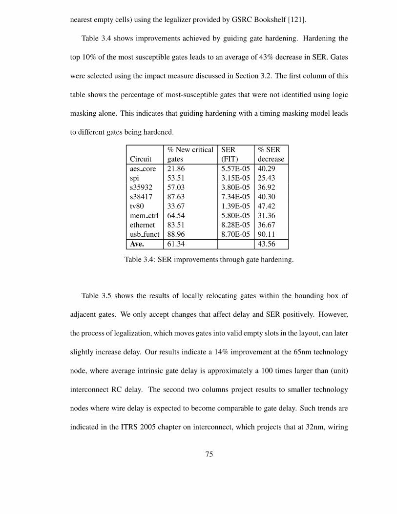
nearest empty cells) using the legalizer provided by GSRC Bookshelf [121].
Table 3.4 shows improvements achieved by guiding gate hardening. Hardening the
top 10% of the most susceptible gates leads to an average of 43% decrease in SER. Gates
were selected using the impact measure discussed in Section 3.2. The first column of this
table shows the percentage of most-susceptible gates that were not identified using logic
masking alone. This indicates that guiding hardening with a timing masking model leads
to different gates being hardened.
% New critical SER % SERCircuit gates (FIT) decreaseaes core 21.86 5.57E-05 40.29spi 53.51 3.15E-05 25.43s35932 57.03 3.80E-05 36.92s38417 87.63 7.34E-05 40.30tv80 33.67 1.39E-05 47.42mem ctrl 64.54 5.80E-05 31.36ethernet 83.51 8.28E-05 36.67usb funct 88.96 8.70E-05 90.11Ave. 61.34 43.56
Table 3.4: SER improvements through gate hardening.
Table 3.5 shows the results of locally relocating gates within the bounding box of
adjacent gates. We only accept changes that affect delay and SER positively. However,
the process of legalization, which moves gates into valid empty slots in the layout, can later
slightly increase delay. Our results indicate a 14% improvement at the 65nm technology
node, where average intrinsic gate delay is approximately a 100 times larger than (unit)
interconnect RC delay. The second two columns project results to smaller technology
nodes where wire delay is expected to become comparable to gate delay. Such trends are
indicated in the ITRS 2005 chapter on interconnect, which projects that at 32nm, wiring
75

65nm < 45nmCircuit %SER % Delay %SER % Delay
decrease increase decrease increaseaes core 11.83 3.00 21.15 -3.10spi 18.87 4.8 41.62 -2.90s35932 10.74 -0.13 44.02 3.40s38417 10.10 1.38 14.35 -11.57tv80 4.89 1.45 43.62 17.50mem ctrl 7.75 1.14 78.43 -1.70ethernet 19.07 0.43 75.17 6.04usb funct 28.50 -5.26 14.29 -9.09Ave. 13.97 0.55 41.59 2.10
Table 3.5: Improvements in SER, through gate relocation.
will contribute 90% of the circuit delay. The first set of results indicates a 14% decrease
in SER, while the second set shows a 41.59% decrease. Therefore, as technology scales,
timing masking can offer greater potential for improvement in SER.
3.6 Summary
We have developed several novel design techniques to improve circuit SER with low
area and performance overhead. Our techniques are based on the careful analysis of the
interplay between signal probability, observability, and masking mechanisms. The first
technique, called SiDeR, finds logical implications between signals, through signature
matching, and adds a few gates to decrease SER. In our second technique, several alternate
non-redundant realizations of the same subcircuit are assessed for global SER improve-
ment and selected based on an objective function that accounts for both SER and area.
Our third technique provides a better method for selecting gates to harden or replicate, by
accounting for errors propagating through the gate. Our fourth technique takes advantage
of improvements in timing masking, by relocating gates (post placement) to minimize their
76

error latching windows. Our results generally show significant improvements in SER, at
low cost.
77

CHAPTER IV
Probabilistic Transfer Matrices
Thus far, we have concentrated on soft-error analysis. Soft errors are a result of rela-
tively rare external-particle strikes or disturbances in circuit behavior. In this chapter, we
move to a more general reliability-analysis framework that treats circuits entirely proba-
bilistically. While this is useful for analyzing soft errors, it is also useful for analyzing
devices that periodically fail or behave probabilistically during regular operation. Quan-
tum dot cellular automata (QCA), where gates and wire are made from ”quantum dots”,
are examples of such devices. Each dot consists of a pair of electrons that can be config-
ured in two different ways to represent a single bit of information. In QCA, both gates and
wires are created from planar arrangements of dots. QCA have an inherent propensity for
faults because the electrons can easily be absorbed into the atmosphere or arrange them-
selves in an ambiguous configuration [62, 104]. Other examples of probabilistic devices
include probabilistic CMOS, molecular logic circuits, and quantum computers.
Historically, the probabilistic analysis of circuits has centered around signal-probability
estimation, which was motivated by random-pattern testability concerns [91], [32], [109].
In short, the probability of a signal being a 0 or 1 gives some indication of the difficulty in
78

controlling (and therefore testing) the signal. In this chapter, we treat circuits probabilisti-
cally to analyze circuit reliability. As opposed to signal probability estimation, reliability
analysis deals with complex probabilistic failure modes and error propagation conditions.
In general, accurate reliability analysis involves computing not just a single output dis-
tribution but, rather, the output error probability for each input pattern. In cases where each
gate experiences input-pattern dependent errors—even if the input distribution is fixed—
simply computing the output distribution does not give the overall circuit error probability.
For instance, if an XOR gate experiences an output bit-flip error, then the output distribu-
tion is unaffected, but the wrong output is paired with each input. Therefore, we need to
separately compute the error associated with each input vector.
Consider the circuit in Figure 4.1. Given that each gate experiences an error with prob-
ability p = 0.1, the circuit’s output error probability for the input combination 000 is 0.244.
The input combination 111 leads to an output error probability of 0.205. The overall error
rate of the circuit is the sum of the error probabilities, weighted by the input combination
probabilities. The probability of error for the circuit in Figure 4.1, given the uniform input
distribution, is therefore 0.225. Note that joint probabilities of input combinations, rather
than individual input probabilities, are necessary to capture correlations among inputs.
We analyze circuit reliability and other aspects of non-deterministic behavior, using
a representation called probabilistic transfer matrix (PTM). A PTM for a gate (or a cir-
cuit) gives the probability of each output combination, conditioned upon the input com-
binations. PTMs can model gates exhibiting varying input-dependent error probabilities.
PTMs form an algebra—a set closed under specific operations—where the operations in
79

question are matrix multiplication and tensor products. These operations may be used to
compute overall circuit behavior by combining gate PTMs to form circuit PTMs. Ma-
trix products capture serial connections, and tensor products capture parallel connections.
Also, PTM-based computations implicitly capture signal correlations that are caused by
fan-out. Most of the concepts and results described in this chapter also appear in [60, 61].
4.1 PTM Algebra
In this section, we describe the PTM algebra and some key operations needed to ma-
nipulate PTMs. First, we discuss the basic operations needed to describe circuits and to
compute circuit PTMs from gate PTMs. Next, we define additional operations to extract
reliability information, eliminate variables, and handle fan-out efficiently. Consider a cir-
cuit C with n inputs and m outputs. We order the inputs for the purposes of PTM represen-
tation and label them in0, . . . inn−1; similarly, the m outputs are labeled out0, . . .outm−1. The
circuit C can be represented by a 2n ×2m PTM M. The rows of M are indexed by an n-bit
vector whose values range from 000 . . .0︸ ︷︷ ︸
nto 111 . . .1
︸ ︷︷ ︸
n. The row indices correspond to input
vectors, i.e. 0/1 truth assignments of the circuit’s input signals. Therefore, if i = i0i1 . . . in
is an n-bit input vector, then row M(i) gives the output probability distribution for n input
values in0 = i0, in1 = i1 . . . inn−1 = in−1. Similarly, column indices correspond to truth as-
signments of the circuit’s m output signals. If j is an m-bit vector, then entry M(i, j) is the
conditional probability that the outputs have values out0 = j0,out1 = j1 . . . outm−1 = jm−1
given input values in0 = i0, in1 = i1 . . . inn−1 = in−1, i.e, P[out puts = j|inputs = i]. There-
fore, each entry in M gives the conditional probability that a certain output combination
occurs given a certain input combination.
80

(F2 ⊗F2 ⊗ I)(I⊗ swap⊗NOTp ⊗ I)(NAND2p⊗NAND2p ⊗ I)(XOR3p)
Figure 4.1: Sample logic circuit and its symbolic PTM formula.
0 1000011010011100101110111
1 00 11 00 10 11 00 11 0
0 1000011010011100101110111
0.756 0.2440.244 0.7560.756 0.2440.244 0.7560.295 0.7050.705 0.2950.295 0.7050.705 0.295
(a) (b)
Figure 4.2: (a) ITM for the circuit in Figure 4.1; (b) circuit PTM, where each gate experi-ences error with probability p = 0.01
Definition 10 Given a circuit C with n inputs and m outputs, the probabilistic transfer
matrix for C is a 2n ×2m matrix M whose entries are M(i, j) = P[out puts = j|inputs = i].
Definition 11 A fault-free circuit has a PTM called an ideal transfer matrix (ITM) in
which the correct logic value of each output occurs with probability 1.
The PTM for a circuit represents its functional behavior for all input and output com-
binations. An input vector for an n-input circuit is a row vector with dimensions 2n × 1.
Entry v(i) of an input vector v represents the probability that the input values in0 = i0, in1 =
i1 . . . inn−1 = in−1 occur. When an input vector is right-multiplied by the PTM, the result is
an output vector of size 1×2m. The output vector gives the resulting output distribution.
81
4.1.1 Basic Operations
PTMs can be defined for all the gates of a logic circuit by taking into account errors
affecting the gates. A PTM for the entire circuit can then be derived from the PTMs of
the gates and their interconnections. The basic operations needed to compute the circuit
PTM from component PTMs are the matrix and tensor products. Consider the circuit C
formed by connecting two gates g1 and g2 in series, i.e., the outputs of g1 are connected
to the inputs of g2. Suppose these gates have PTMs M1 and M2; then the entry M(i, j)
of the resulting PTM M for C represents the probability that g2 produces output j, given
g1 has input i. This probability is computed by summing over all values of intermediate
signals (outputs of g1 which are also inputs of g2) for input i of g1 and output j of g2.
Therefore, each entry M(i, j) = ∑all l M1(i, l)M2(l, j) This operation corresponds to the
ordinary matrix product M1M2 of the two component PTMs.
Now suppose that circuit C is formed by two parallel gates g1 and g2 with PTMs M1 and
M2. Each entry in the resulting matrix M should represent the joint conditional probability
of a pair of input-output values from g1 and a pair of input-output values from g2. Each
such entry is therefore a product of independent conditional probabilities from M1 and M2,
respectively. These joint probabilities are given by the tensor product operation.
Definition 12 Given two matrices M1 and M2, with dimensions 2k × 2l and 2m × 2n, re-
spectively, the tensor product M = M1 ⊗M2 of M1 and M2 is a 2km × 2ln matrix whose
entries are:
M(i0 . . . ik+m−1, j0 . . . jl+n−1) = M1(i0 . . . ik−1, i0 . . . jl−1)×M2(ik . . . ik+m−1, jl . . . jl+n−1)
.
82

(a)
1 01 01 00 1
⊗
1 00 10 10 1
=
1 0 0 00 1 0 00 1 0 00 1 0 01 0 0 00 1 0 00 1 0 00 1 0 01 0 0 00 1 0 00 1 0 00 1 0 00 0 1 00 0 0 10 0 0 10 0 0 1
(b)
Figure 4.3: Illustration of the tensor product operation: (a) circuit with parallel AND andOR gates; (b) circuit ITM formed by the tensor product of the AND and ORITMs.
Figure 4.3 shows the tensor product of an AND ITM with an OR ITM. Note that the OR
ITM appears once for each occurrence of a 1 in the AND ITM; this is a basic feature of
the tensor product.
Besides the usual logic gates (AND, OR, NOT , etc.), it is useful to define three special
gates for circuit PTM computation. These are (i) the n-input identity gate, with ITM
denoted In; (ii) the n-output fan-out gate Fn; and (iii) the swap gate, swap. These wiring
PTMs are shown in Figure 4.1.
An n-input identity gate simply outputs its input values with probability 1. It cor-
responds to a set of independent wires or buffers and has the 2 × 2 identity matrix as
its ITM. Larger identity ITMs can be formed by the tensor product of smaller identity
ITMs. For instance, the ITM for a 2-input, 2-output identity gate is I2 = I ⊗ I. More
generally, Im+n = Im ⊗ In. An n-output fan-out gate, Fn, copies an input signal to its n
83

[1 00 1
] [1 0 0 00 0 0 1
]
swap =
1 0 0 00 0 1 00 1 0 00 0 0 1
(a) (b) (c)
Figure 4.4: Wiring PTMs: (a) identity gate (I) ; (b) 2-output fan-out gate (F2); (c) adjacentswap gate (swap).
2
2
b
c d
a
e
g
h
f
L1 L2 L3 L4
(F2 ⊗F2 ⊗ I)(I⊗ swap⊗NOTp ⊗ I)(NAND2p⊗NAND2p ⊗ I)(XOR3p)
Figure 4.5: Circuit to illustrate PTM calculation; vertical lines separate levels of the cir-cuit; the parenthetical subexpressions correspond to logic levels.
outputs. The ITM of a 2-output fan-out gate, shown in Figure 4.1b, has entries of the form
F2(i0, j0 j1) = 1, where i0 = j0 = j1 and all other entries are 0. Therefore, the 5-output fan-
out ITM, F5, has entries F5(0,00000) = F5(1,11111) = 1, with all other entries 0. Wire
permutations, such as crossing wires, are represented by swap gates. The ITM for an ad-
jacent wire swap (a simple two-wire crossover) is shown in Figure 4.1c. Any permutation
of wires can be modeled by a network of swap gates.
Example 5 Consider the circuit in Figure 4.5—this is the same circuit as in Figure 4.1,
with the wiring gates made explicit. The PTMs for the gates with error probability p are
as follows:
84

p 1− pp 1− pp 1− p
1− p p
1− p pp 1− pp 1− p
1− p pp 1− p
1− p p1− p p1− p p
[p 1− p
1− p p
]
NAND2p XOR3p NOTp
The circuit PTM is expressed symbolically by the formula in Figure 4.5. Each parenthe-
sized term in the equation corresponds to a level in the circuit. The advantage of evaluat-
ing the circuit PTM using such an expression is that the error probabilities for the entire
circuit can be extracted from it.
4.1.2 Additional Operations
In addition to the basic operations of matrix multiplication and tensor product, we
introduce the following three operations to increase the scope and efficiency of PTM-based
computation:
• fidelity: This operation measures the similarity between an ITM and a corresponding
PTM. It is used to evaluate the reliability of a circuit.
• eliminate variables: This operation computes the PTM of a subset of inputs or out-
puts, starting from a given PTM. It can also be used to compute the probability of
error of individual outputs.
• eliminate redundant variables: This operation eliminates redundant input variables
that result from tensoring matrices of gates that are in different fan-out branches of
the same signal
85

We now formally define and describe these operations in more detail. First, we define
the element-wise product used in computing fidelity.
Definition 13 The element-wise product of two matrices A and B, both of dimension n×m,
is denoted A.∗B = M and defined by M(i, j) = A(i, j)×B(i, j).
To obtain the f idelity, the element-wise product of the ITM and the PTM is multiplied
on the left by the input vector, and the norm of the resulting matrix is computed. In the
definition below, ||v|| denotes the l1 norm of vector v.
Definition 14 Given a circuit C with PTM M, ITM J, and input vector v, the fidelity of M
is given by
f idelity(v,M,J) = ||v(M.∗ J)||
The fidelity of a circuit is a measure of its reliability. Figure 4.6 illustrates the f idelity
computation on the circuit from Figure 4.1. The ITM, shown in Figure 4.2a, is denoted J,
and the PTM, shown in Figure 4.2b, is denoted M.
vT =
0.1250.1250.250.25000.1250.125
J.∗M =
0.756 00 0.7560.756 00 .7560 0.7050.705 00 0.7050.705 0
v(J.∗M) =[
0.567 0.177]
(a) (b) (c)
Figure 4.6: Matrices used to compute f idelity for the circuit in Figure 4.1: (a) input vector;(b) result of element-wise multiplication of its ITM and PTM; (c) result of left-multiplication by the input vector.
86

Example 6 Consider the circuit C from Figure 4.1, with inputs {w,x,y} and output {z} .
The circuit PTM is calculated using the PTMs from Example 5, with probability of error
p = 0.05 at each gate, on all inputs. Figure 4.6 shows intermediate matrices needed for
this computation. The quantity f idelity(v,M,J) is found by first element-wise multiplying
J and M, then left-multiplying by an input vector v. The l1 norm of the resulting matrix is
f idelity(v,M,J)= (0.567+0.177)= 0.743. The probability of error is 1−0.743 = 0.257.
The eliminate variables operation is used to compute the ”sub-PTM” of a smaller set
of input and output variables. We formally define it for 1-variable elimination.
Definition 15 Given a PTM matrix M that represents a circuit C with inputs in0 . . . inn−1,
eliminate variables(M, ink) is the matrix M′ with n−1 input variables
in0 . . . ink−1ink+1 . . . ink+1 . . . inn−1 whose rows are
M′(i0 . . . ik−1ik+1 . . . in−2, j) = M(i0 . . . ik−1 0 ik+1 . . . in−2, j)+M(i0 . . . ik−1 1 ik+1 . . . in−2, j)
The eliminate variables operation is similarly defined for output variables. 1 The
elimination of two variables can be achieved by eliminating each of the variables individ-
ually, in arbitrary order. Figure 4.7 demonstrates the elimination of column variables from
a subcircuit C′ of the circuit in Figure 4.5, formed by the logic between inputs w,x and
outputs g,h. The PTM for C′ with probability of error p = 0.05 on all its gates is given by:
(F2 ⊗F2)(swap⊗NOTp)(NAND2p⊗NAND2p)
1The eliminate variables operation is analogous to the existential abstraction of a set of variables x ina Boolean function f [37], given by the sum of the positive and negative cofactors of f , with respect to x:∃x f = fx + fx. The eliminate variables operation on PTMs relies on arithmetic addition of matrix entriesinstead of the Boolean disjunction of cofactors.
87
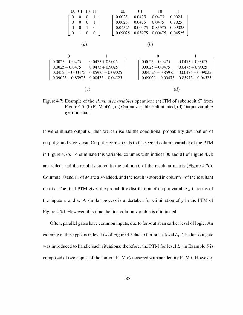
00 01 10 11
0 0 0 10 0 0 10 0 1 00 1 0 0
00 01 10 11
0.0025 0.0475 0.0475 0.90250.0025 0.0475 0.0475 0.90250.04525 0.00475 0.85975 0.090250.09025 0.85975 0.00475 0.04525
(a) (b)
0 1
0.0025+0.0475 0.0475+0.90250.0025+0.0475 0.0475+0.90250.04525+0.00475 0.85975+0.090250.09025+0.85975 0.00475+0.04525
0 1
0.0025+0.0475 0.0475+0.90250.0025+0.0475 0.0475+0.90250.04525+0.85975 0.00475+0.090250.09025+0.00475 0.85975+0.04525
(c) (d)
Figure 4.7: Example of the eliminate variables operation: (a) ITM of subcircuit C ′ fromFigure 4.5; (b) PTM of C′; (c) Output variable h eliminated; (d) Output variableg eliminated.
If we eliminate output h, then we can isolate the conditional probability distribution of
output g, and vice versa. Output h corresponds to the second column variable of the PTM
in Figure 4.7b. To eliminate this variable, columns with indices 00 and 01 of Figure 4.7b
are added, and the result is stored in the column 0 of the resultant matrix (Figure 4.7c).
Columns 10 and 11 of M are also added, and the result is stored in column 1 of the resultant
matrix. The final PTM gives the probability distribution of output variable g in terms of
the inputs w and x. A similar process is undertaken for elimination of g in the PTM of
Figure 4.7d. However, this time the first column variable is eliminated.
Often, parallel gates have common inputs, due to fan-out at an earlier level of logic. An
example of this appears in level L3 of Figure 4.5 due to fan-out at level L1. The fan-out gate
was introduced to handle such situations; therefore, the PTM for level L1 in Example 5 is
composed of two copies of the fan-out PTM F2 tensored with an identity PTM I. However,
88

this method of handling fan-out can be computationally inefficient because it requires
numerous matrix multiplications. Therefore, in either inputs or outputs we introduce a
new operation called eliminate redundant variables to remove redundant signals that are
due to fan-out or other causes. This operation is more efficient than matrix multiplication
because it is linear in PTM size, whereas matrix multiplication is cubic.
Definition 16 Given a circuit C with n inputs in0, . . . inn−1, and PTM M, let ink and inl be
two inputs that are identified with (connected to) each other. Then
eliminate redundant variables(M, ink, inl) = M′, where M′ is a matrix with n− 1 input
variables whose rows are
M′(i1 . . . ik . . . il−1 il+1 . . . in−1, j) = M(i1 . . . ik . . . il−1 ik il+1 . . . in−1, j)
The definition of eliminate redundant variables can be extended to a set of input variables
that are redundant. Figure 4.8 shows an example of the eliminate redundant variables
operation.
PTMs yield correct output probabilities despite reconvergent fan-out because the joint
probabilities of signals on different fan-out branches are computed correctly using the
tensor product and eliminate redundant variables operations. Suppose two signals on
different fan-out branches reconverge at the same gate in a subsequent circuit level. Since
the joint probability distribution of these two signals is computed correctly, the serial com-
position of the fan-out branches with the subsequent gate is also correct, by the properties
of matrix multiplication. On the other hand, if the individual signal probabilities are com-
puted separately, then these probabilities cannot be recombined into the joint probability
without some loss of accuracy.
89
000001010011100101110111
1 0 0 00 1 0 01 0 0 00 1 0 01 0 0 00 1 0 00 0 1 00 0 0 1
00011011
1 0 0 00 1 0 01 0 0 00 0 0 1
(a) (b) (c)
Figure 4.8: Signal forwarding using eliminate redundant variables: (a) circuit with sig-nal b fanning out to two different levels; (b) NAND⊗ I, adding b as an inputand output; (c) final ITM for circuit computed by removing rows in boldface.
The eliminate redundant variables operation can efficiently handle fan-out to differ-
ent levels by ”signal forwarding,” as seen in Figure 4.8. Signal b is required at a later level
in the circuit; therefore, b is added to the ITM as an output variable by tensoring the AND
ITM with an identity matrix. However, tensoring with the identity ITM adds both an input
and output to the level. Hence, the additional input is redundant with respect the second
input of the AND gate and is removed using eliminate redundant variables. Note that
the removed rows correspond to assigning contradictory values on identical signals.
4.1.3 Handling Correlations
There are many cases of errors where input and output values cannot be separated
and combinations of these values must be taken into account. For example, using the
eliminate variables operation, the conditional probabilities of the inputs or outputs cannot
always be stored separately in different matrices. While such storage can alleviate the
input-space explosion inherent in storing all possible combinations of inputs and outputs,
it may not capture correlations within the circuit.
Example 7 Suppose two wires have a 0.25 probability of swapping. The matrix corre-
90

1 0 0 00 0.75 0.25 00 0.25 0.75 00 0 0 1
1 00.75 0.250.25 0.750 1
1 0 0 00.752 (0.75)(0.25) (0.25)(0.75) 0.252
0.252 (0.75)(0.25) (0.25)(0.75) 0.752
0 0 0 1
(a) (b) (c)
Figure 4.9: Example of output inseparability: (a) PTM for a probabilistic wire-swap; (b)PTM for each individual output after applying eliminate variables; (c) incor-rect result from tensoring two copies of the PTM from part (b) and applyingeliminate redundant variables.
sponding to this error is given in Figure 4.9a. If we try to separate the probability of each
output, using eliminate variables, the output probabilities both have the PTM of Figure
4.9b. If these outputs are tensored (with redundant inputs eliminated), they result in the er-
roneous combined matrix of Figure 4.9c. This demonstrates that these two outputs cannot
be correctly separated; their joint conditional distributions are, in fact, inseparable.
Just as some errors cannot be separated, some faults affect multiple gates simultane-
ously. In this case, the combined PTM cannot be built from individual PTMs, and the joint
probabilities must be obtained (or the exact correlation determined). This same effect can
occur with input vectors, which cannot always be separated into probabilities of individual
inputs. An example is given below.
00 01 10 11[
0.5 0 0 0.5]T
PTMs have the advantage that, at every level, they can represent and manipulate joint
probabilities from the inputs to the outputs. If necessary, individual output distributions
can be obtained using the eliminate variables operation.
91

So far, we have introduced the PTM representations of gate and wire constructs, and
the operations needed to combine them into circuit PTMs. In the next section, we give
examples of the various kinds of faults that PTMs can capture, as well as the application
of PTMs in soft-error analysis and error-threshold computation.
4.2 Applications
In this section, we discuss applications of PTMs to various fault types as well as in
determining the error-transfer behavior of logic circuits.
4.2.1 Fault Modeling
The PTM model can represent a wide variety of faulty circuit behaviors, including
both hard and soft errors. The fact that there are separate probabilities for each input and
output, and the fact that they are propagated simultaneously make this possible. Figure
4.10 lists some errors that can be represented by PTMs.
000011010011100101110111
1 01 01 00 10 11 00 10 1
000011010011100101110111
1 01 01 00 11 01 01 00 1
000011010011100101110111
1 01 00 11 01 00 10 10 1
000011010011100101110111
0.95 0.050.95 0.050.95 0.050.05 0.950.05 0.950.95 0.050.05 0.950.05 0.95
000011010011100101110111
1 00 10 11 00 11 00 11 0
(a) (b) (c) (d) (e)
Figure 4.10: PTMs for various types of gate errors: (a) a fault-free ideal 2-1 MUX gate;(b) first input signal stuck-at 1; (c) first two input signals swapped; (d) prob-abilistic output bit-flip with p = 0.05; (e) wrong gate: MUX replaced by3-input XOR gate.
Figure 4.10a shows the ITM for a fault-free ideal 2-1 multiplexer (MUX). Figure
92

4.10b shows the first data input signal of the MUX stuck-at 1, i.e., row 000 is replaced
with row 100 of the ITM, row 010 with row 111, and so forth. Figure 4.10c shows an
example with the first two wires swapped; this is captured by permuting the rows of the
ITM, accordingly. Figure 4.10d shows the first example of a probabilistic error, an output
bit-flip where the wrong value occurs with probability p = 0.05 in each row. Figure 4.10e
shows a design error where a MUX has been replaced by an XOR gate. As these examples
indicate, PTMs can capture both gate errors and wiring errors.
PTMs can also represent errors that are likely to occur in nanoscale circuits. For in-
stance, in QCA, the wires themselves are made of ”quantum dots,” and so, like gates, wires
can experience bit-flips. Bit-flips on wires can be represented by the 1-input identity gate
I, with probabilistic errors as shown below.
1− p p
1 1−q
As mentioned in Chapter I, adjacent wires in nanoscale CMOS circuits can suffer
from crosstalk. When two adjacent wires run parallel to each other, there is capacitive
and inductive coupling, which can cause neighboring signals to erroneously switch [96].
Crosstalk can be represented by a faulty 16×2 matrix, which takes transitions rather than
signal values into account. Hence, we need circuit information for two consecutive time
units.
Consider the circuit shown in Figure 4.11. Let a0,b0, . . .y0,z0 denote signals at time
unit t0 and a1,b1, . . .y1,z1 denote the same signals at time t0. Suppose we identify f and g
as likely candidates for crosstalk faults, with f being the aggressor signal and g being the
victim. If f transitions from 0 to 1, then due to crosstalk, g also has a chance of erroneously
93

Figure 4.11: Circuit to illustrate crosstalk faults.
0000000100100011010001010110011110001001101010111100110111101111
1 00 11 00 1
1− p p0 1p 1− p0 11 0p 1− p1 0p 1− p1 00 11 00 1
Figure 4.12: Representing a crosstalk error using PTMs.
transitioning similarly. This is represented by the PTM with inputs f0, f1,g0,g1 and output
g′1 which contains an erroneous transition with probability p, as shown in Figure 4.12.
While we have explicitly modeled various types of errors in conventional CMOS
nanoscale circuits, we have not modeled errors whose probabilities change dynamically.
For instance, we do not model time-varying error probabilities or errors whose probabil-
ities are described by probability-distribution functions (PDFs). However, in the future,
using PTMs it may be possible to model such cases. For instance, in order to use PTMs
94
with entries formed by PDFs, the tensor and matrix multiplications operations will need
to be redefined to handle sums (convolutions) and products of probability distributions.
However, as we show in the next section, if error probabilities depend on specifically iden-
tifiable discrete variables, apart from the input variables, these too can be incorporated into
PTMs.
4.2.2 Modeling Glitch Attenuation
Thus far, signals have been described by their logic value, with each signal represented
by a 1× 2 vector that indicates the probability of it being 0 or 1. While retaining the
discreteness of our model, we now expand signal representation to incorporate necessary
electrical characteristics.
For instance, we can differentiate between signals of long and short duration just
as we differentiate between signals with high and low amplitude (by their logic value).
We can represent a signal by a vector w which has four entries instead of two, w =
[p0s p0l p1s p1l ]. The second bit of the row index represents short (“s”) or long (”l”) du-
ration, so p0s is the probability of a logic 0 with short duration. Extraneous glitches, such
as those induced by SEUs, are likely to have short duration, while driven logic signals are
likely to have relatively long duration.
Each gate in a circuit has a probability of an SEU strike that depends upon various
environmental factors, such as neutron flux and temperature. We call this the probability
of occurrence for a gate (or node) g, and denote it by poccur(g). However, SEU strikes cre-
ate glitches which can be differentiated by a combination of shape and amplitude. These
differentiations are important in the propagation of a glitch through circuit gates. There-
95

fore, we utilize a modified identity matrix known as I1,n(poccur) to represent a probability
distribution on a glitch induced by an SEU strike.
We use the specific glitch-propagation model from [88] to determine which signal
characteristics to capture; a different model might require other characteristics to be repre-
sented. In [88], glitches are classified into three types, depending on their duration D, and
amplitude A, relative to the gate propagation delay Tp, and threshold voltage Vt . Glitches
are assumed to change only logic-0 to logic-1 when they strike (but can later be inverted).
• Glitches of type 1 have amplitude A > Vt and duration D > 2Tp. Glitches of this type
are propagated without attenuation.
• Glitches of type 2 have amplitude A > Vt and duration 2Tp > D > Tp. Glitches of
this type are propagated with an attenuated amplitude of A′ < A.
• Glitches of type 3 have A < Vt . Glitches of this type are not propagated, i.e., they
are electrically masked.
Since amplitude is already indicated by the logic value, we need an additional bit
to indicate whether the duration is larger or smaller than the propagation delay of the
gate (when the amplitude is higher than the threshold voltage). The duration is irrelevant
for glitches with amplitude lower than the threshold voltage, since these are likely to be
attenuated. Figure 4.13a shows the probability distribution of an SEU strike when the
correct logic value is 0. Glitches of type 1 are indicated by row labels 11, glitches of types
2 are indicated by labels 10, and glitches of type 3 are indicated by 01. In particular, Figure
4.13a assumes uniform distribution, with respect to glitches.
96
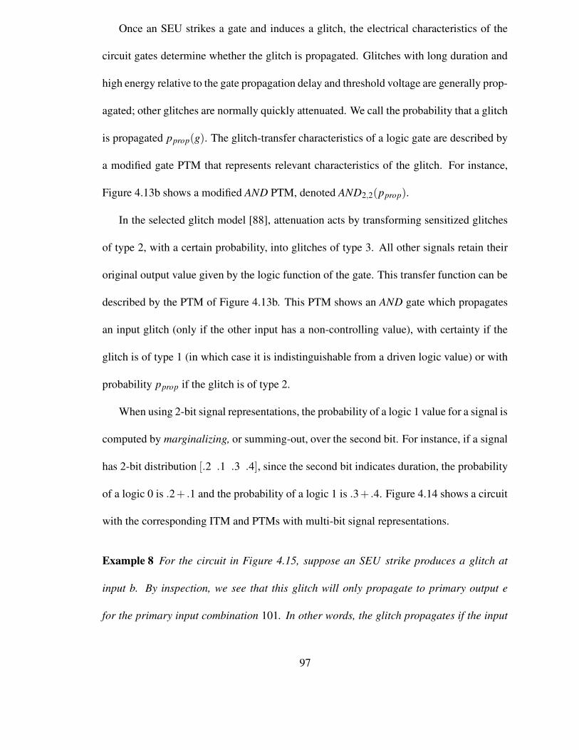
Once an SEU strikes a gate and induces a glitch, the electrical characteristics of the
circuit gates determine whether the glitch is propagated. Glitches with long duration and
high energy relative to the gate propagation delay and threshold voltage are generally prop-
agated; other glitches are normally quickly attenuated. We call the probability that a glitch
is propagated pprop(g). The glitch-transfer characteristics of a logic gate are described by
a modified gate PTM that represents relevant characteristics of the glitch. For instance,
Figure 4.13b shows a modified AND PTM, denoted AND2,2(pprop).
In the selected glitch model [88], attenuation acts by transforming sensitized glitches
of type 2, with a certain probability, into glitches of type 3. All other signals retain their
original output value given by the logic function of the gate. This transfer function can be
described by the PTM of Figure 4.13b. This PTM shows an AND gate which propagates
an input glitch (only if the other input has a non-controlling value), with certainty if the
glitch is of type 1 (in which case it is indistinguishable from a driven logic value) or with
probability pprop if the glitch is of type 2.
When using 2-bit signal representations, the probability of a logic 1 value for a signal is
computed by marginalizing, or summing-out, over the second bit. For instance, if a signal
has 2-bit distribution [.2 .1 .3 .4], since the second bit indicates duration, the probability
of a logic 0 is .2+ .1 and the probability of a logic 1 is .3+ .4. Figure 4.14 shows a circuit
with the corresponding ITM and PTMs with multi-bit signal representations.
Example 8 For the circuit in Figure 4.15, suppose an SEU strike produces a glitch at
input b. By inspection, we see that this glitch will only propagate to primary output e
for the primary input combination 101. In other words, the glitch propagates if the input
97

Tp
glitch due to SEU
attenuated glitchDA’
A
00001011
1− poccur poccur/3 poccur/3 poccur/30 1 0 00 0 1 00 0 0 1
(a)
00,0000,0100,1000,1101,0001,0101,1001,1110,0010,0110,1010,1111,0011,0111,1011,11
1 0 0 01 0 0 01 0 0 01 0 0 01 0 0 01 0 0 01 0 0 01 0 0 01 0 0 01 0 0 00 1− pprop pprop 01 0 0 00 1 0 01 0 0 00 1− pprop pprop 00 0 0 1
(b)
Figure 4.13: PTMs for SEU modeling where the row labels indicate input signal type: (a)I2,2(poccur) describes a probability distribution on the energy of an SEU strikeat a gate output, (b) AND2,2(pprop) describes SEU-induced glitch propaga-tion for a 2-input AND gate. The type-2 glitches become attenuated to type3 with a probability 1− pprop.
98

CircuitITM = (I1,2 ⊗F2,2 ⊗ I1,2)(AND2,2(pprop)⊗AND2,2(pprop))(F2,2⊗ I1,2)(I1,2⊗AND2,2(pprop))CircuitPTM = (I1,2 ⊗F2,2 ⊗ I1,2)(AND2,2(pprop)I1,2(poccur)⊗AND2,2(pprop)I1,2(poccur))
(F2,2 ⊗ I1,2)(I1,2⊗AND2,2(pprop)I1,2(poccur))
Figure 4.14: Circuit with ITM and PTMs describing an SEU strike and the resultant prop-agation with multi-bit signal representations.
Figure 4.15: Circuit used in Example 8 to illustrate the incorporation of electrical maskinginto PTMs.
sensitizes the appropriate path to d and then e. If we let poccur = 0.001 and pprop = 0.5,
and AND2,2(pprop) is as shown in Figure 4.13, then the circuit PTM is given by:
(I2 ⊗ I2,2(poccur)⊗ I2)(AND2,2(pprop)⊗ I2)(AND2,2(pprop))
The corresponding PTM and fidelity are given in Figure 4.16.
f idelity = .99994791
Perror = 1− f idelity = .000052083
4.2.3 Error Transfer Function
In this section, we analyze circuit reliability as a function of gate reliability. Using data
points for various gate error values, we derive low-degree polynomial approximations for
99

1 0 0 0...1 0 0 0
0.9996 0.0001 0.0003 00.9996 0.0002 0.0002 0
1 0 0 01 0 0 01 0 0 01 0 0 01 0 0 01 0 0 0
0.2500 0.1875 0.5625 00.2500 0.3750 0.3750 0
1 0 0 01 0 0 0
0.5000 0.1250 0.3750 00.5000 0.2500 0.2500 0
1 0 0 01 0 0 0
0.9995 0.0002 0.0003 00.9995 0.0001 0.0001 0.0003
1 0 0 01 0 0 01 0 0 01 0 0 01 0 0 01 0 0 00 0.1250 0.3750 00 0.2500 0.2500 01 0 0 01 0 0 00 0.5000 0.5000 00 0 0 1
Figure 4.16: PTM for the circuit used in Example 8 which incorporates electrical proper-ties of the gates.
the error transfer functions of standard benchmark circuits. Such functions can be used to
derive upper bounds for tolerable levels of gate error.
Definition 17 The error transfer function e(x) on 0 ≤ x ≤ 1 of a circuit C is the fidelity of
C with output-error probability x on all gates.
Figure 4.17 illustrates the error-transfer functions for several standard benchmark cir-
cuits, determined by introducing varying amounts of error into gates and then calculating
the circuit fidelity according to Definition 14. Generally, such error transfer curves can
be described by polynomials. If two gates have error p, then their composition (series,
parallel, or a combination of both) has terms that are linear combinations of p2 and p,
100
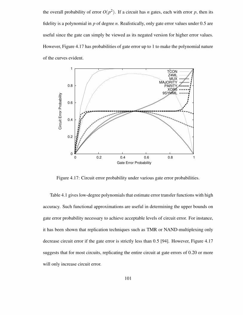
the overall probability of error O(p2). If a circuit has n gates, each with error p, then its
fidelity is a polynomial in p of degree n. Realistically, only gate error values under 0.5 are
useful since the gate can simply be viewed as its negated version for higher error values.
However, Figure 4.17 has probabilities of gate error up to 1 to make the polynomial nature
of the curves evident.
0
0.2
0.4
0.6
0.8
1
0 0.2 0.4 0.6 0.8 1
Circ
uit E
rror P
roba
bility
Gate Error Probability
TCONZ4MLMUX
MAJORITYPARITY
XOR59SYMML
Figure 4.17: Circuit error probability under various gate error probabilities.
Table 4.1 gives low-degree polynomials that estimate error transfer functions with high
accuracy. Such functional approximations are useful in determining the upper bounds on
gate error probability necessary to achieve acceptable levels of circuit error. For instance,
it has been shown that replication techniques such as TMR or NAND-multiplexing only
decrease circuit error if the gate error is strictly less than 0.5 [94]. However, Figure 4.17
suggests that for most circuits, replicating the entire circuit at gate errors of 0.20 or more
will only increase circuit error.
101

Polynomial coefficientsCircuit Error a0 a1 a2 a3 a4 a5 a6majority 2.5 E-7 0.2080 0.1589 0 0 0 0 0mux 6.6 E-6 0.0019 1.9608 -2.8934 1.9278 0 0 0parity 0.0040 0.0452 5.4892 -21.4938 31.9141 -4.2115 -30.3778 19.5795tcon 0.0019 0.0152 6.2227 -13.5288 7.1523 9.2174 -9.0851 09symml 0.0010 0.0250 2.4599 -3.7485 1.5843 0 0 0xor5 0.0043 0.0716 5.9433 -26.4666 51.1168 -44.6143 14.4246 0
Table 4.1: Polynomial approximations of circuit error transfer curves and residual errors.The fitted polynomials are of the form e(x) ≈ a0 +a1x+a2x2 +a3x3 . . ..
4.3 Summary
In this chapter, we proposed the probabilistic transfer matrix (PTM) to capture non-
deterministic behavior in logic circuits. PTMs provide a concise description of both nor-
mal and faulty behavior and are well-suited to reliability analysis. A few simple composi-
tion rules based on connectivity can be used to recursively build larger PTMs representing
entire logic circuits from smaller gate PTMs. PTMs can accurately calculate joint output
probabilities in the presence of reconvergent fan-out and inseparable joint input distri-
butions. In addition, we defined new matrix operations to eliminate variables, remove
redundancy, and compute the overall probability of circuit error. We showed how PTMs
can be used to capture various sorts of errors inherent in nanocircuits, including soft errors.
We also used PTMs to derive polynomial approximations for circuit error probabilities in
terms of gate error probabilities for the purpose of determining thresholds of acceptable
gate error for specific circuits.
102

CHAPTER V
Computing with PTMs
Circuit PTMs have exponential space complexity because they contain information
about all possible input vectors. Their complexity makes numerical computation with
PTMs impractical for circuits with more than 10-15 inputs. In order to improve scala-
bility, we develop an implementation of the PTM framework that uses algebraic decision
diagrams (ADDs) to compress matrices. We also derive several ADD algorithms to com-
bine PTMs directly in their compressed forms.
Figure 4.2 gives a PTM for the circuit in Figure 4.1 along with the corresponding ADD,
representing the case where all gates experience output bit-flips with probability p = 0.1.
As the figure shows, the same values occur multiple times in the matrix and suggest a
possibility of compression. Due to the canonicity of ADD/BDD representation, identical
subgraphs, corresponding to identical submatrices, can be identified and eliminated dur-
ing the process of ADD-construction. In some cases, ADDs contain exponentially fewer
nodes than the number of entries in the explicit matrix representation. In such cases,
linear-algebraic transformations can be applied exponentially faster to the ADD than to
the matrix.
103

Developing efficient ADD algorithms for PTM operations is a significant technical
challenge that we address in this chapter. We adapt previous ADD algorithms from [8]
and [123] for tensor and matrix products. The original versions of their algorithms handle
only square matrices, while PTMs are generally rectangular. In addition, we develop ADD
algorithms for the new operations defined in Chapter IV. These operations are necessary
for computing marginal-probability distributions, reconciling dimensions, and estimating
overall circuit-error probabilities.
In the second part of this chapter, we develop several methods to further improve the
scalability of PTM-based analysis. These methods employ the following techniques: parti-
tioning and hierarchical computation, dynamic evaluation ordering, and input-vector sam-
pling. Most of the techniques and results described in this chapter also appear in [60, 61].
5.1 Compressing with Decision Diagrams
This section discusses the compression of PTMs using algebraic decision diagrams
(ADDs), and develops a procedure for computing circuit PTMs from gate PTMs.
Recall that a binary decision diagram (BDD) is a directed acyclic graph representing a
Boolean function f (x0,x1,x2, . . .xn) with root node x0. The subgraph formed by the outgo-
ing edge labeled 0 represents the negative cofactor fx′0(x1 . . .xn), or the else BDD. The sub-
graph formed by the outgoing edge labeled 1 represents the positive cofactor fx0(x1 . . .xn),
or the then BDD. Boolean constants are represented by terminal nodes.
ADDs are variants of BDDs in which terminal nodes can take on any real value. Bahar
et al. [8] present a method of encoding a matrix, using an ADD. The ADD encoding of a
matrix M is a rooted directed acyclic graph whose entries depend on the row- and column-
104

index variables (r0,c0,r1,c1 . . .rn,cn) of M; branches of the ADDs correspond to portions
of the matrix. The root of the ADD is the node labeled r0. The subgraph formed by the
outgoing edge labeled 0 represents the top half of M, i.e., the half corresponding to r0 = 0.
The subgraph formed by the outgoing edge labeled 1 represents the bottom half of M,
which has r0 = 1. As in BDDs, the same path can encode several entries if variables are
skipped. The input variables are queried in a pre-defined order and facilitate reductions,
through the use of a single subgraph for identical submatrices.
We use the QuIDDPro library [123] to encode PTMs as ADDs. We also added func-
tions to this library for perform operations on PTMs. QuIDDPro includes the CUDD
library [117] and uses interleaved row and column variable ordering, which facilitates fast
tensor products and matrix multiplications—key operations in the quantum-mechanical
simulations for which QuIDDPro was designed. The basic ADD functions used in PTM
computations are as follows.
• topvar(Q) : returns the root node of an ADD Q
• then(Q) : returns the 1 branch
• else(Q) : returns the 0 branch
• ite(Q,T,E): refers to the i f -then-else operation, which takes a node Q correspond-
ing to the root and two ADDs, T and E, corresponding to the then and else branches,
and combines them into a larger ADD.
All matrix algorithms for ADDs, that we are aware of, assume square matrices but can
represent non-square matrices using zero padding [8, 26]. Zero-padding is necessary in
105

ADDs to distinguish between missing row (or column) variables and those that do not exist
because of matrix dimensions—a non-square matrix has fewer row variables than column
variables, or vice versa. Recall that ADD variables are ordered, and nodes are levelized
by decision variables. Any variable missing from the ADD can be wrongly interpreted
as marking replicated matrix entries; Figure 5.1 illustrates a situation in which missing
variables can create ambiguity.
0 1
p 1− pp 1− pp 1− p
1− p p
00 01 10 11
p 1− p p 1− pp 1− p p 1− pp 1− p p 1− p
1− p p 1− p p
(a) (b)
Figure 5.1: PTMs with identical ADDs without zero-padding: (a) matrix with only onecolumn variable; (b) matrix without dependency on the second column vari-able.
Figure 5.2 describes an algorithm for padding matrices with zeros. This algorithm
assumes that there are more row variables than column variables but can easily be modified
to handle cases with more column variables than row variables. Suppose a PTM with
ADD A has 2m+1 rows and 2m columns. The zero padding of A is done by introducing a
new node, q, with then(q) pointing to the original ADD and else(q) pointing to the zero
terminal. In Figure 5.2, the function shi f t col var labels, by shifting the column variable
number up to facilitate the introduction of missing variables into the ADD, renames nodes
representing column variables.
The introduction of zero padding is sufficient to implement the matrix multiplication
operation. However, the tensor products of zero-padded PTMs are generally incorrect.
106
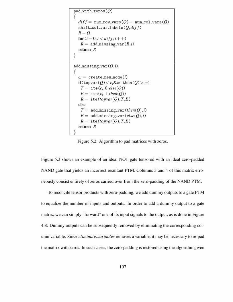
pad with zeros(Q)
{di f f = num row vars(Q)− num col vars(Q)
shift col var labels(Q,di f f)R = Qfor(i = 0; i < di f f ; i++)
R = add missing var(R, i)return R
}
add missing var(Q, i){
ci = create new node(i)if(topvar(Q)< ci&& then(Q)> ci)
T = ite(ci,0,else(Q))E = ite(ci,1, then(Q))R = ite(topvar(Q),T,E)
elseT = add missing var(then(Q), i)E = add missing var(else(Q), i)R = ite(topvar(Q),T,E)
return R}
Figure 5.2: Algorithm to pad matrices with zeros.
Figure 5.3 shows an example of an ideal NOT gate tensored with an ideal zero-padded
NAND gate that yields an incorrect resultant PTM. Columns 3 and 4 of this matrix erro-
neously consist entirely of zeros carried over from the zero-padding of the NAND PTM.
To reconcile tensor products with zero-padding, we add dummy outputs to a gate PTM
to equalize the number of inputs and outputs. In order to add a dummy output to a gate
matrix, we can simply ”forward” one of its input signals to the output, as is done in Figure
4.8. Dummy outputs can be subsequently removed by eliminating the corresponding col-
umn variable. Since eliminate variables removes a variable, it may be necessary to re-pad
the matrix with zeros. In such cases, the zero-padding is restored using the algorithm given
107

[0 11 0
]
(a)
⊗
0 1 0 00 1 0 00 1 0 01 0 0 0
(b)
=
0 0 0 0 0 1 0 00 0 0 0 0 1 0 00 0 0 0 0 1 0 00 0 0 0 1 0 0 00 1 0 0 0 0 0 00 1 0 0 0 0 0 00 1 0 0 0 0 0 01 0 0 0 0 0 0 0
(c)
Figure 5.3: (a) NOT gate ITM; (b) zero-padded NAND gate ITM; (c) their tensor productwith incorrect placement of all-zero columns.
in Figure 5.2.
5.1.1 Computing Circuit PTMs
We present an algorithm for computing the ADD of a circuit’s PTM in Figure 5.4,
following the method illustrated in Example 5 of Chapter IV. First, a gate library is
specified in the form of a set of gate PTMs. The circuit (in BLIF format) is read into
a data structure that stores its individual gates and wiring structure. The gates are reverse-
topologically sorted, from primary outputs to primary inputs, and the subsequent compu-
tation proceeds by topological level. Next, the gate PTMs are converted to ADDs. The
ADDs for gates at each level are tensored together, zero-padding is performed, and finally,
the eliminate redundant variables operation is applied to eliminate dummy outputs. The
ADD representing each level, called levelADD in Figure 5.4, is multiplied with the accu-
mulated circuit ADD computed thus far, which is called circuitADD. After all levels are
multiplied together, the computation of the circuitADD is complete. An added subtlety is
that the signals of adjacent levels have to be properly aligned, i.e., the outputs of current
level have to match with the inputs of the previous level in order for the multiplication to
108

be performed correctly; this can be done by appropriately permuting the row and column
variables of the ADDs.
A detail not shown in Figure 5.4 is that when a circuit has fan-out branches to multiple
levels, the gate is placed at the first level at which it is needed, and its output is forwarded
to other levels using the method shown in Figure 4.8. The intermediate-level ADDs are
discarded after they are multiplied with the circuitADD. This is important for the scalabil-
ity of the implementation because levelADDs are the tensor products of several gate ADDs
and can have large memory complexity.
In place of fan-out gates, we use the eliminate redundant variables operation (Defini-
tion 16), whose ADD implementation is given in Figure 5.5. By removing each duplicated
(due to fan-out) input signal, the number of levels decreases and multiplications are saved.
Previously computed partial results of the eliminate redundant variables operation are
stored in a common hash table, which is searched first to avoid traversing common paths
or recomputing existing results.
In Figure 5.5, capitalized variables refer to ADDs, and lower-case variables refer to
nodes. This algorithm searches the ADD, starting from the root, for the first of two re-
dundant variables v1,v2 with v1 < v2 in the ADD node ordering. Whenever v1 is found on
a path, it traverses down then(v1) until v2 is found. It eliminates the v2 node and points
the preceding node to then(v2). Next, it traverses down else(v1) and searches for v2; this
time it eliminates v2 and points the preceding node to else(v2). This process can be re-
peated in cases where there are more redundant variables. Both eliminate variables and
eliminate redundant variables are operations that can disturb the equality between row
109

struct gate
{PTM[][]
node *ADD
DDmanager M
}
compute circuit ADD(circuit C, errors E){
gatemap = read into gates(C)sort topological levels(gatemap)add errors(gatemap,E)for(each gate g ∈ gate map)
gatemap[g].ADD = convert to ADD(gatemap[g].PTM)
pad with zeros(gatemap[g])for(each level l ∈ gatemap)
levelgates = order outputs by previous level inputs(l)for(each gate h ∈ levelgates)
levelADD = tensor ADD(levelADD,h.ADD)
zero track(levelADD)
redvars = find redundant inputs(levelADD)
eliminate redundant variables(levelADD,redvars)circuitADD = multiply ADD(circuitADD, levelADD)
delete(levelADD)return circuitADD
}
Figure 5.4: Algorithm to compute the ADD representation of a circuit PTM. The gatestructure stores a gate’s functional information, including its PTM, inputnames, output names, and ADD.
and column variables, since they both remove variables. Therefore, it may be necessary to
introduce zero-padding. (Figure 5.2).
Once the ADD for the PTM and ITM of a circuit is known, we can compute the f idelity
of the circuit to extract reliability information (see Figure 5.6). The f idelity algorithm first
takes the element-wise product of the ADD for the ITM with the ADD for the PTM, and
then performs a depth-first traversal to sum probabilities of correctness. The traversal
of the ADD sums the terminal values while keeping track of skipped nodes. A skipped
110

node in an ADD is an indication that the terminal value is repeated for 2x times, where
x depends on the skipped variable’s ordering. Note that the ADD implementations of
eliminate redundant variables, f idelity, and eliminate variables run in linear time in
the size of the ADDs in their arguments.
Characteristics Reliability, p = 0.05 No. Stats., p = 0 Stats., p = 0.05Circuit No Width Two One ADD Mem. Time Mem. Time
gates -way -way nodes (MB) (s) (MB) (s)C17 6 5 0.846 0.880 2.00E3 1.090 0.002 0.071 0.313mux 6 23 0.907 0.939 1.35E4 26.13 3.109 8.341 2.113z4ml 8 20 0.670 0.817 7.01E3 6.594 1.113 3.030 0.8400x2 12 23 0.150 0.099 2.85E4 11.015 2.344 237.9 10.52parity 15 23 0.602 0.731 1.96E3 1.060 0.113 0.337 0.262pcle 16 16 0.573 0.657 5.46E5 28.59 6.160 4.196E1 4.300decod 18 13 0.000 0.000 2.76E4 30.15 1.020 5.690E2 11.80cu 23 23 0.461 0.579 1.06E5 13.39 2.176 2.155E1 3.430pm1 24 27 0.375 0.596 4.55E5 77.66 5.031 2.155E2 13.349symml 44 37 0.327 0.534 1.05E7 4445 552.7 5.341E3 696.2xor5 47 19 0.067 0.071 4.67E4 46.72 3.539 10.556E3 19.58
Table 5.1: Statistics on various small benchmarks.
Results from the calculation of circuit ITMs, PTMs, and f idelity are listed in Table
5.1. We used the smaller LGSynth 91 and LGSynth 93 benchmarks with uniform input
distributions. These simulations were conducted on a Linux workstation with a 2GHz Pen-
tium 4 processor. In these experiments, CPU time was limited to 24 hours. The runtimes
and memory requirements are sensitive to the width of a circuit, i.e., the largest number
of signals at any level. Empirically, circuits with widths of around 40 signals can be eval-
uated. In these experiments, we calculate entire circuit PTMs, i.e., output probabilities
for all input combinations. If we separated output cones and calculated individual output
probabilities, the results would scale much further. However, as discussed before, individ-
ual output probabilities cannot always be accurately combined to obtain the overall error
probability of a circuit. The number of ADD nodes required for the f idelity computation
111

eliminate redundant variables(Q,v1,v2){
if(isconstant(Q)) return Qif(topvar(Q)== v1)
T = comp remove branch(then(Q),v2,1)E = comp remove branch(else(Q),v2,0)
elseif(topvar(then(Q))≤ v1)
T = comp remove branch(then(Q),v2,1)else
T = eliminate redundant variables(then(Q),v1,v2)if(topvar(else(Q))≤ v1)
E = comp remove branch(else(Q),v2,0)else
E = eliminate redundant variables(else(Q),v1,v2)R = ite(topvar(Q),T,E)return R
}
comp remove branch(Q,v2,const){
if(table lookup(Q,v2,const) ! = NULL)return table lookup(Q,v2,const)
if(topvar(Q)== v2)if(const == 1)return then(Q)
else return else(Q)
else if(topvar(Q) ≤ v2)return Q
elseT = comp remove branch(then(Q),v2,const)E = comp remove branch(else(Q),v2,const)R = ite(topvar(Q),T,E)table insert(R,Q,v2,const)
return R}
Figure 5.5: Algorithm to eliminate redundant variables.
is also listed in Table 5.1, including intermediate computations.
Table 5.1 gives the overall probability of correctness for circuits with gate error proba-
bilities of 0.05 and also for one-way gate errors with probability 0.05. In CMOS gates, an
112

compute fidelity(Q1,Q2,v){
Q3 = apply(Q1,Q2,∗)R = multiply ADD(v,Q3)P = sum probs(R,1)return P
}
sum probs(Q,mult){
if(table lookup(Q,mult) ! = NULL)return table lookup(Q,mult)
sum = 0mult∗= 2if(isconstant(Q))
return value(Q)∗multif(topvar(Q)+1! = topvar(then(Q)))
multt = multt +2sum+ = sum probs(then(Q),multt)
if(topvar(Q)+1! = topvar(else(Q)))multe = mult +2sum+ = sum probs(else(Q),multe)table insert(sum,Q,mult)return sum
}
Figure 5.6: Algorithm to compute f idelity.
erroneous output value 0 is more likely than an erroneous value 1 because SEUs typically
short-circuit power to ground. PTMs can easily encode this bias since error probabilities
can be different for different input combinations. Relevant empirical results are given in
the ”one-way” column of Table 5.1. Circuits with a high output-to-input ratio, such as
decod.blif, tend to magnify gate errors at fan-out stems and, therefore, have higher error
probabilities.
PTM computation for p = 0.05 requires more memory and longer runtime because less
compression is possible. Ideal transfer matrices have large blocks of 0s, which lend them-
113

selves to greater compression. When gate PTMs with error probabilities are composed in
various ways, PTMs with a greater number of distinct entries are created, thus yielding
less compression. Compare the values in the ITM and PTM shown in Example 6. Our
results indicate that, while exact and complete circuit-PTM computation cannot be used
to evaluate industry-sized circuits, it can be used to calibrate or validate other reliability
evaluation tools.
5.2 Improving Scalability
We have presented ADD algorithms for PTM-based computation, but their scalability
appears limited due to the possibility of combinatorial explosion in PTM size. Scalability
can be improved in a variety of different ways. In this section, we cover several techniques,
starting from methods of speeding up exact-PTM computation and moving to heuristic
methods that approximate the circuit’s error probability.
In Section 5.2.1, we propose to improve the efficiency of PTM computation by pre-
scheduling an evaluation order for combining gate PTMs into circuit PTMs. While the
evaluation order does not affect the final result, it can decrease the sizes of intermediate
matrices. Good evaluation orders compute PTMs for clusters of gates with a small number
inputs and outputs in between the clusters. In effect, such an ordering would enclose fan-
out branches and reconvergences within the clusters.
In Section 5.2.2, we use exact-PTM computations for partitions in a circuit (instead of
the whole circuit) and propagate signal and error probabilities between the partitions. This
method allows exact computations to be maximally used while approximating the overall
error rate. In Section 5.2.3, we briefly discuss methods of sampling, i.e., computing the
114

average error probability of a randomly generated set of input vectors to estimate the true
error probability.
5.2.1 Dynamic Evaluation Ordering
The ADD-based multiplication algorithm used in our PTM algebra implementation,
from [8], has a major impact on the efficiency of PTM computations. The worst-case time
and memory complexity of the multiplication operation is O((|A||B|)2), for two ADDs A
and B. The PTM evaluation algorithm described in Figure 5.4 first tensors gates for each
level to form level PTMs and then multiplies the level PTMs, thereby creating relatively
large multiplication instances. Smaller instances can be created by rescheduling the order
of evaluation and delaying the tensor product as long as possible.
Figure 5.7: Tree of AND gates used in Example 9 to illustrate the effect of evaluationordering on computational efficiency.
Example 9 Consider the tree of AND gates in Figure 5.7. Suppose we wish to compute its
circuit PTM. The algorithm of Figure 5.4 requires topologically sorting the gates, calculat-
115

ing the PTM for each level, and multiplying together the levels in order. The levels are L4 =
{G15},L3 = {G14,G13},L2 = {G12,G11,G10,G9},L1 = {G8,G7,G6,G5,G4,G3,G2,G1}.
The corresponding level PTMs have dimensions 22 × 2,24,22,28 × 24, and 216 × 28, re-
spectively. We denote the Li PTM as Mi. First, we compute M3×M4, which is of dimension
24×2; next, M2 is multiplied by M3 ×M4, yielding a matrix of size 28×2; and so on. The
dimensions of the matrix product instances are as follows: (22 ×2,24 ×22),(24×2,28 ×
24),(28×2,216×28). In the worst case, when ADD sizes are close to matrix sizes (in gen-
eral, they are smaller, as ADDs provide compression), the total memory complexity of the
multiplications is 250 +234 +218. On the other hand, separating the gates (not tensoring)
for as long as possible, starting from the primary inputs, yields the matrix multiplication
instances of the following sizes: 4(24 × 22,22 × 2),2(24 × 2,22 × 2),and(28 × 2,22 × 2).
Here, the total memory complexity is only 220 +227 +242. Therefore, carefully scheduling
matrix multiplication leads to a more efficient PTM computation algorithm.
If the output of a source gate is connected to more than one sink gate, there are two
possibilities for evaluation ordering: the first is to tensor gates PTMs and eliminate the
redundant variables; the second possibility is to process gates and logic cones separately
until they need to be tensored at a different level to facilitate a multiplication. We choose
the latter approach, which exchanges multiplications for tensor products. This is advan-
tageous, as the tensor product has lower complexity than multiplication. Determining the
optimal order to multiply levels is similar to solving the matrix chain multiplication prob-
lem [27], which can be solved by a dynamic programming algorithm in O(n3) time. Our
application can use the same algorithm; the cost of multiplying two matrices is estimated
116

based on their dimensions, without taking ADD compression into account.
Improved ordering Levelized orderingCircuit Time(s) Memory(MB) Time(s) Memory(MB)C17 0.212 0.000 1.090 0.004mux 18.052 2.051 26.314 3.109z4ml 3.849 1.004 6.594 1.113x2 11.015 2.344 193.115 12.078parity 1.060 0.113 1.07 0.133pcle 28.810 3.309 98.586 6.160decod 5.132 1.020 30.147 24.969cu 23.700 2.215 13.385 2.176pm1 72.384 3.734 77.661 5.031cc 57.400 4.839 1434.370 155.6609symml 89.145 6.668 4445.670 552.668xor5 3.589 0.227 46.721 3.539b9 9259.680 165.617 23164.900 295.984c8 35559.500 930.023 mem-out mem-out
Table 5.2: Comparison of runtimes and memory usage for levelized ordering and orderingcomputed by dynamic programming.
The results of applying the improved ordering for multiplication of levels are given
in Table 5.2. The data in this table were produced on a Pentium 4 processor running at
2GHz. In general, this ordering method uses less memory, with only a modest increase
in runtime. The runtime increase seen in Table 5.2 is partially due to the overhead of the
dynamic programming. However, this tradeoff is acceptable since memory was the main
bottleneck.
5.2.2 Hierarchical Reliability Estimation
In this section, we extend PTM analysis hierarchically to estimate the reliability of
larger circuits partitioned into subcircuits. This allows for the use of exact PTM com-
putation for smaller partitions, and provides a way of estimating the error on the entire
circuit.
117

First, the ITMs and PTMs of all subcircuits are calculated. Then, in topological order,
we calculate the fidelities and output probabilities on each subcircuit output individually.
We call the individual fidelity of an output bit its bit- f idelity. Since evaluation proceeds in
topological order, input bit- f idelities are already calculated for the previously processed
subcircuits.
In order to formally define bit-fidelity, we introduce the abstract operation for nota-
tional convenience.
Figure 5.8: Circuit used in Example 10 to illustrate hierarchical reliability estimation .
Definition 18 For a PTM M and an output variable ok, M′ = abstract(M,k) is the matrix
which results from the elimination of all variables except ok from M. Therefore, M′ =
eliminate variables(M,0,1,2 . . .k−1,k +1 . . .m)
Definition 19 The bit-fidelity of output ok of circuit C, with ITM J, PTM M, and input dis-
tribution v, is the probability of error of the kth output bit. It is given by bit f idelity(k,v,J,M) =
f idelity(vk,Jk,Mk), where Jk = abstract(J,k), Mk = abstract(M,k), and vk = abstract(v,k)
118

Suppose the input bit-fidelities for the inputs of a particular subcircuit are p1, p2, p3 . . . pn.
Then, in order to account for input error, the subcircuit PTM is multiplied by Ip1⊗Ip2 . . . Ipn ,
where Ip has the form
p 1− p
1− p p
.
The probability distribution of each signal is also calculated by multiplying the input distri-
bution of each subcircuit by its ITM and then abstracting each of the output probabilities.
The algorithm details are given in Figure 5.9, where SubCircArray is the topologically
sorted array of subcircuits, PIs is the list of primary inputs, POs is the list of primary
outputs, Distro stores the separated probability distribution of intermediate variables, and
the Bfid array contains the bit-fidelities of previously processed signals. At each iteration,
Bfid is updated with output bit-fidelities of the current subcircuit. At the termination of the
algorithm, Bfid contains the bit-fidelities of the primary outputs.
This algorithm has several interesting features. First, it only calculates PTMs of sub-
circuits and, thus, avoids the state-space explosion associated with directly computing the
entire circuit’s PTM. For instance, if a circuit with n inputs and m outputs is partitioned
into two subcircuits each with n/2 inputs and m/2 outputs, the PTMs of the two subcircuits
together are of size 2(2(n+m)/2), which is significantly smaller than the circuit PTM, which
has size 2n+m. Second, the algorithm approximates joint probability distributions, using
marginal probability distributions, and averages local error probabilities at each subcircuit.
Any loss of accuracy is a result of the abstract operation and the averaging effect which oc-
curs in bit-fidelity calculations. Therefore, the estimation technique will be very accurate
in cases where there is no reconvergent fan-out between the subcircuits. In fact, the error
probabilities are exact when each output bit has the same error on all input combinations
119

estimate bit fidelity(input V, circuit C){topological sort(C)for(each primary input in ∈C)
B f id[in] = 0Distro[in] = abstract(V, in)partition circuit(C)for(each partition S ∈C)
J = calc itm(S)M = calc ptm(S)for(each input in ∈ S)Vin[S] = tensor ADD(Vin[S],Distro[in])Vout[S] = multiply ADD(Vin[S],J)
for(each output out ∈ S)Distro[out] = abstract(Vout[S], j)
for(each input in ∈ S)I′ = tensor ADD(M′,create I matrix(B f id[in]))
M′ = multiply ADD(I ′,M)
for(each output out ∈ S)B f id[out] = bit fidelity(out,Distro[out],J,M′)
}
Figure 5.9: The Bit f idelity estimation algorithm.
120
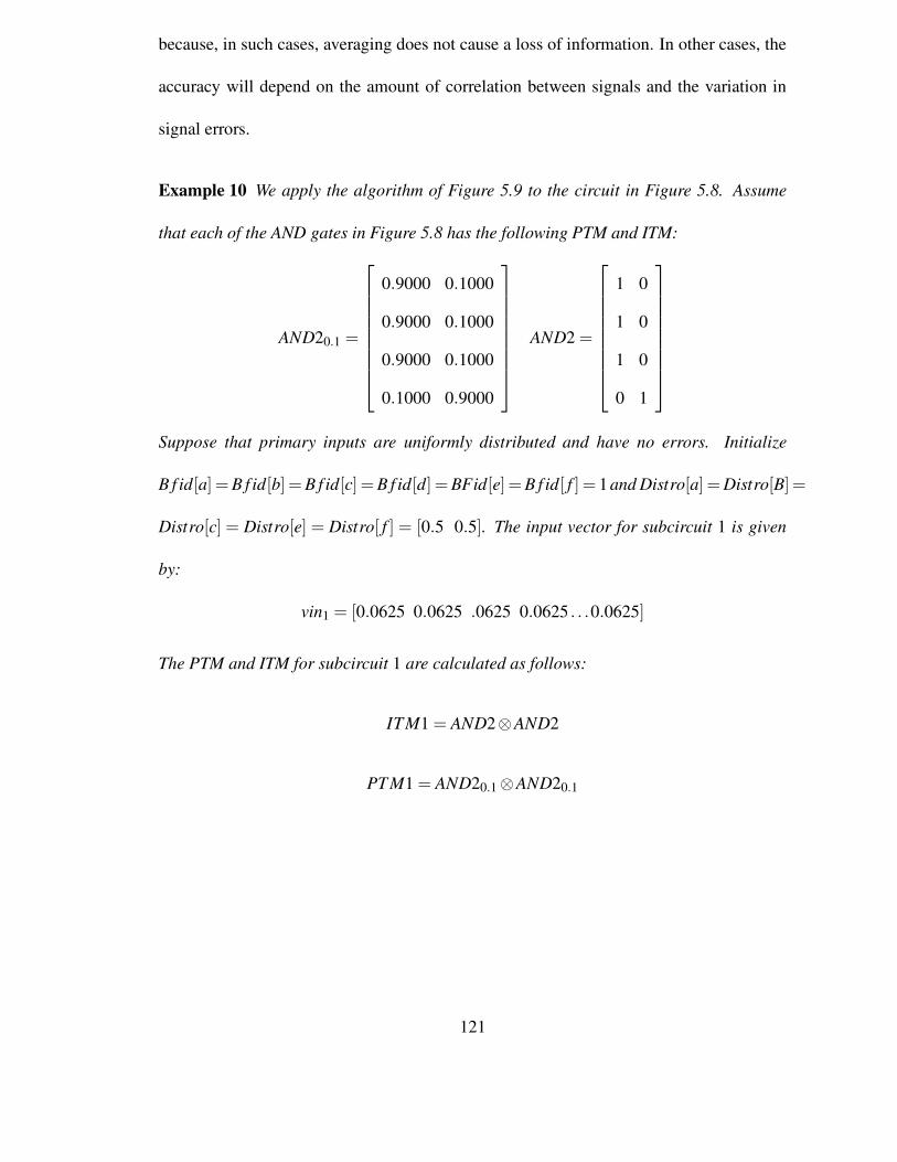
because, in such cases, averaging does not cause a loss of information. In other cases, the
accuracy will depend on the amount of correlation between signals and the variation in
signal errors.
Example 10 We apply the algorithm of Figure 5.9 to the circuit in Figure 5.8. Assume
that each of the AND gates in Figure 5.8 has the following PTM and ITM:
AND20.1 =
0.9000 0.1000
0.9000 0.1000
0.9000 0.1000
0.1000 0.9000
AND2 =
1 0
1 0
1 0
0 1
Suppose that primary inputs are uniformly distributed and have no errors. Initialize
B f id[a] = B f id[b] = B f id[c] = B f id[d] = BFid[e] = B f id[ f ] = 1 and Distro[a] = Distro[B] =
Distro[c] = Distro[e] = Distro[ f ] = [0.5 0.5]. The input vector for subcircuit 1 is given
by:
vin1 = [0.0625 0.0625 .0625 0.0625 . . .0.0625]
The PTM and ITM for subcircuit 1 are calculated as follows:
ITM1 = AND2⊗AND2
PT M1 = AND20.1 ⊗AND20.1
121

ITM1 =
1 0 0 01 0 0 01 0 0 00 1 0 01 0 0 01 0 0 01 0 0 00 1 0 01 0 0 01 0 0 01 0 0 00 1 0 00 0 1 00 0 1 00 0 1 00 0 0 1
PTM1 =
0.81 0.09 0.09 0.010.81 0.09 0.09 0.010.81 0.09 0.09 0.010.09 0.81 0.01 0.090.81 0.09 0.09 0.010.81 0.09 0.09 0.010.81 0.09 0.09 0.010.09 0.81 0.01 0.090.81 0.09 0.09 0.010.81 0.09 0.09 0.010.81 0.09 0.09 0.010.09 0.81 0.01 0.090.09 0.01 0.81 0.090.09 0.01 0.81 0.090.09 0.01 0.81 0.090.01 0.09 0.09 0.81
The fidelity and probability distribution for each output of subcircuit 1 are calculated
as follows:
vout1 = vin1 ∗ ITM1 = [0.5625 0.1875 0.1875 0.0625]
Distro[g] = abstract(vin1,g) = [0.75 0.25]
Distro[h] = abstract(vin1,h) = [0.75 0.25]
PT M1′ = (I(1)⊗ I(1)⊗ I(1)⊗ I)∗PTM1 = PT M1
B f id[g] = bit f idelity(g,Distro[g],PTM1′, ITM1) = 0.9
B f id[h] = 0.9
Similarly for subcircuit 2:
IT M2 = (I ⊗AND2⊗ I)(I⊗F2 ⊗ I)(AND2⊗AND2)(AND2)
PT M2 = (I ⊗AND20.1 ⊗ I)(I⊗F2 ⊗ I)(AND20.1 ⊗AND20.1)(AND20.1)
PT M2′ = (I⊗ I0.9 ⊗ I0.9 ⊗ I)(PTM2)
vin2 = [0.5 0.5]⊗ [0.75 0.25]⊗ [0.75 0.25]⊗ [0.5 0.5]
122

ITM2 =
1 01 01 01 01 01 01 01 01 01 01 01 01 01 01 00 1
PTM2 =
0.8920 0.10800.8856 0.11440.8920 0.10800.8856 0.11440.8920 0.10800.8856 0.11440.8920 0.1080.8344 0.16560.8856 0.11440.8280 0.17200.8856 0.11440.8280 0.17200.8856 0.11440.8280 0.17200.8344 0.16560.3160 0.6840
PTM2′ =
0.8920 0.10800.8851 0.11490.8920 0.10800.8810 0.11900.8920 0.10800.8810 0.11900.8920 0.10800.8441 0.15590.8851 0.11490.8229 0.17710.8810 0.11900.7819 0.21810.8810 0.11900.7819 0.21810.8441 0.15590.4133 0.5867
vout2 = [0.9922 0.0078]
Distro[l] = [0.9922 0.0078]
BFid[l] = bit f idelity(l,Distro[l],PTM2′, ITM2) = 0.869
Alternatively, using the circuit PTM to calculate the fidelity gives f idelity = 0.862. This
has an error of only 0.003 for gate errors in the range 0.1.
The f idelity of the entire circuit (rather than just its output bits) can be further esti-
mated by using the binomial probability distribution to calculate the probability that any
output signal has an error. This once again assumes that output signals are independent.
5.2.3 Approximation by Sampling
Reliability estimation requires computing the error associated with each input combi-
nation. Like SER analysis, reliability analysis can also be approximated by sampling input
vectors. This sampling can be done in several ways. We briefly discuss two methods of
sampling which yield estimates of the overall circuit error probability.
123

The first method is to sample input and output vectors without computing circuit or
component PTMs. This method is akin to replacing the TSA/TMSA fault models of Chap-
ter II with a more general PTM-based fault model (where the error probabilities depend on
the input values) and then using the same methods of bit-parallel sampling. This provides
a link between signature-based approximate analysis and PTM-based exact analysis. The
algorithm from Figure 2.7 can be used to compute the error probability, with a slight mod-
ification. Instead of flipping bits of signatures with constant probabilities at each gate, we
can flip signatures with probabilities conditioned on the input values (as indicated by the
appropriate row of the gate PTM).
A second method of sampling involves computing the exact output distribution for
each input vector but generating the set of input vectors to sample randomly. Computing
the exact output vector for an input vector is fairly complicated in and of itself. However,
it does scale to much larger circuits than circuit PTM computation. The algorithm for
computing the output vector for a given input vector, using vector-PTM multiplication and
tensoring, is described in Chapter VI.
5.3 Summary
To improve computational efficiency, we encoded PTMs as algebraic decision dia-
grams (ADDs). We also developed equivalent ADD algorithms for our newly defined
matrix operations that can be used to compute circuit fidelity and to obtain marginal error
probabilities for subsets of outputs. We also developed methods to handle non-square ma-
trices, which were not represented as decision diagrams in past literature. In addition, we
presented several heuristic methods for improving the scalability of PTMs, including sam-
124

pling, partitioning, evaluation ordering, and hierarchical computations which allow PTM
computations to scale to larger circuits.
125

CHAPTER VI
Testing for Probabilistic Faults
After circuits are manufactured, it is important to insure that they do not have unusually
high sensitivity to soft errors. While the SER of a circuit can be analyzed during or after
design, the error rate can be significantly increased because of variability in the manufac-
turing process. Therefore, circuits have to be tested in order to ensure that their soft error
rates do not exceed an acceptable threshold. To estimate the expected soft error rate in the
field, chips are typically tested while exposed to intense beams of protons or neutrons, and
the resulting error rate is measured. However, these types of tests often take a long time
to conduct because random patterns may not be sensitive to vulnerabilities in the circuit.
In this section, we develop methods selecting test vectors such that test application time is
minimized.
Generating tests for probabilistic faults is fundamentally different from previous test-
ing techniques. Traditionally, the goal of testing has been to detect the presence of defects.
A set of test vectors is normally applied to the inputs of a circuit and the resultant outputs
are compared to correct pre-computed outputs to determine whether a fault is present. In
contrast, the goal of probabilistic testing is the estimation of error probability. Probabilistic
126

testing requires a multiset (a set with repetitions) of test patterns, since a given fault is only
present for a fraction of the computational cycles. Another difference is that some test
vectors detect transient faults with higher probability than others due to path-dependent
effects like electrical masking. Therefore, one can consider the likelihood of detection, or
the sensitivity, of a test vector to a fault. Table 6.1 summarizes these differences.
Attribute Deterministic Testing Probabilistic TestingFault type Deterministic Transient or intermittentFault model Stuck-at, bridging, etc Probabilistic generalizationTest inputs Set of input vectors Multiset of input vectorsCoverage Faults detected with certainty Faults detected with varying probabilitiesGoal Detect fault presence Estimate fault probability
Table 6.1: Key differences between deterministic and probabilistic testing.
In Section 6.1, we define and provide computation methods for test-vector sensitivity to
faults. Section 6.2 provides integer linear programming (ILP) formulations for generating
a compact set of test vectors for probabilistic faults. Most of the concepts and results in
this chapter also appear in [53, 54].
6.1 Test-Vector Sensitivity
In this section, we discuss the sensitivity of test vectors to transient faults. We be-
gin with an example and then present a PTM-based algorithm for test-vector sensitivity
computation.
Example 11 Consider the circuit in Figure 6.1. If an SEU occurs with a certain proba-
bility at input b, then the test vectors that propagate the induced error to the outputs are:
t1 = 001 (to output Y ), t2 = 100 (to output Z), and t3 = 101 (to both Y and Z).
127

Figure 6.1: Circuit to illustrate test-vector sensitivity computation.
In deterministic testing, any test vector that detects a fault can be chosen. However,
error attenuation along sensitized paths affects the propagation of probabilistic faults. If
the propagation probability is pprop at each gate, then t1 has probability pt1 = p2prop of
propagating the error to an output, t2 has probability pt2 = pprop, and t3 has probability
pt3 = pt1 + pt2 − pt1 pt2 . For a fault that occurs with probability p f , a vector ti has to be
repeated d1/(pti ∗ p f )e times for one expected detection. Therefore, test application time
will be shortest for test vector t3. Vector t3 is said to be the most sensitive to the transient
fault in question.
Since PTMs can encode a wide variety of faults, including faults with path-based
effects, test-vector sensitivity computed with PTMs can take these effects into account.
There are two ways to compute the sensitivity of a test vector. The first is by circuit-PTM
computation, which is explained in Chapter IV. Here, the gate PTMs are combined to
form a circuit PTM, and the most sensitive test vectors correspond to the PTM rows with
the lowest probability of correctness.
We can formally define the sensitivity of a test vector to faults in the circuit using
PTMs. The sensitivity of a test vector t to a multi-fault set F = { f1, f2, . . . fn} which occurs
128

with probability P = {p1, p2, . . . pn} in circuit C with PTM MF and ITM M is defined as
the total probability that the output under t is erroneous, given that faults F exist with
probability P. A test vector t can be represented by the vector vt , with 0’s in all but the
index corresponding to t’s input assignments. For instance, if a test vector t assigns 0’s
to all input signals and C has 3 inputs, then vt = [1 0 0 0 0 0 0 0]. The sensitivity
of t is the probability that the ideal and faulty outputs are different, and this is computed
by taking the norm of the element-wise product (Definition 13) of the correct and faulty
output vectors. This operation is similar to the f idelity operation of Chapter IV, defined
for vectors rather than matrices.
sens(F, t) = 1−||(vtM f ).∗ (vtM)||l1(6.1)
The sensitivity of test vector
vt = [1 0 0 0 0 0 0 0]
for the circuit in Figure 6.1, with the probability of error p = 0.1, can be computed from
the circuit’s ITM M, and PTM MF , as shown in Figure 6.2. Here, both the correct and
faulty output vectors are computed and the results are compared to obtain the sensitivity.
Note that vtM f and vtM need to be marginalized if there is a multi-bit signal represen-
tation. For instance, in the case of the SEU model of Chapter IV, the second bit needs to
be summed out for both of the vectors to obtain the correct sensitivity.
The second method of sensitivity computation is through output vector computation
for a particular test vector. Here, we begin with a pre-selected complete set of test vectors
for the permanent stuck-at faults corresponding to those in F . For each test vector in this
129

vt ×MF = vt ×
0.8100 0.0900 0.0820 0.01800.8100 0.0900 0.0820 0.01800.8100 0.0900 0.0820 0.01800.8100 0.0900 0.0180 0.08200.8100 0.0900 0.0820 0.01800.8100 0.0900 0.0820 0.01800.0900 0.0100 0.7380 0.16200.0900 0.0100 0.1620 0.7380
=
0.81000.09000.08200.0180
T
vt ×M = vt ×
1 0 0 01 0 0 01 0 0 01 0 0 01 0 0 01 0 0 00 0 1 00 0 0 1
=[
1 0 0 0]
sens(F, t) = 1−||[1 0 0 0].∗ [0.81 0.09 0.082 0.018]||
= 1−||[0.81 0 0 0]|| = 1− (.81) = 0.9
Figure 6.2: Sensitivity computation on the circuit of Figure 6.1.
130
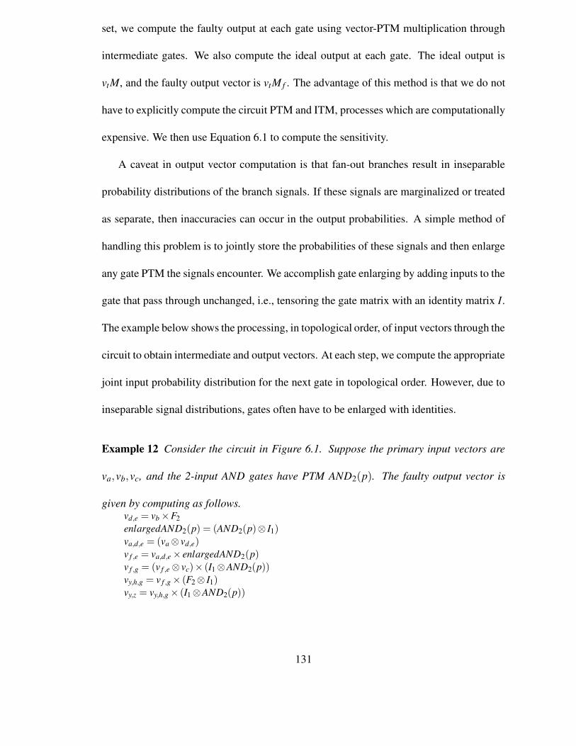
set, we compute the faulty output at each gate using vector-PTM multiplication through
intermediate gates. We also compute the ideal output at each gate. The ideal output is
vtM, and the faulty output vector is vtM f . The advantage of this method is that we do not
have to explicitly compute the circuit PTM and ITM, processes which are computationally
expensive. We then use Equation 6.1 to compute the sensitivity.
A caveat in output vector computation is that fan-out branches result in inseparable
probability distributions of the branch signals. If these signals are marginalized or treated
as separate, then inaccuracies can occur in the output probabilities. A simple method of
handling this problem is to jointly store the probabilities of these signals and then enlarge
any gate PTM the signals encounter. We accomplish gate enlarging by adding inputs to the
gate that pass through unchanged, i.e., tensoring the gate matrix with an identity matrix I.
The example below shows the processing, in topological order, of input vectors through the
circuit to obtain intermediate and output vectors. At each step, we compute the appropriate
joint input probability distribution for the next gate in topological order. However, due to
inseparable signal distributions, gates often have to be enlarged with identities.
Example 12 Consider the circuit in Figure 6.1. Suppose the primary input vectors are
va,vb,vc, and the 2-input AND gates have PTM AND2(p). The faulty output vector is
given by computing as follows.vd,e = vb ×F2enlargedAND2(p) = (AND2(p)⊗ I1)va,d,e = (va ⊗ vd,e)v f ,e = va,d,e × enlargedAND2(p)v f ,g = (v f ,e ⊗ vc)× (I1 ⊗AND2(p))vy,h,g = v f ,g × (F2 ⊗ I1)vy,z = vy,h,g × (I1 ⊗AND2(p))
131

Additionally, note that signal probabilities incorporate the effects of reconvergent fan-
out from b to z, since signals in the fan-out branch (d,g, f ,x,z) were always jointly rep-
resented and processed. However, storing joint probability distributions can be computa-
tionally expensive; therefore, in some cases a loss of accuracy may be traded in favor of
memory complexity reduction.
An algorithm for computing the output of a test vector under probabilistic faults (en-
coded in gate PTMs) is shown in Figure 6.3. The primary input values, determined by the
given test vectors, are converted into input vectors. Then, in topological order, the inputs
for each gate are tensored together to form the input vector for the gate. If any of the
input signals are stored jointly with other signals, the gate in question is enlarged by the
number of additional signals. The gate PTM is multiplied by the input vector to obtain
the output vector. In the case of a multiple-output gate such as a fan-out gate, the output
vector stays as a joint probability distribution. In practice, output distributions can become
very large, through the accumulation of correlated signals. However, the joint signals can
be separated by using the eliminate variables operation, which may entail some loss of
accuracy.
This process can be repeated with gate ITMs (or functional simulation) to obtain the
ideal output vector. Finally, test vector sensitivity is computed according to Equation 6.1,
using the f idelity algorithm of Figure 5.6 applied to the ideal and faulty primary-output
vectors. Table 6.2 shows average runtime and memory usage statistics for test vector
sensitivity computation for various input vectors on standard benchmark circuits from the
ISCAS85 suite. These simulations were conducted on a Linux workstation with an Intel
132

compute faulty output(Circuit C, testvector T){
for(all inputs i ∈C)vector[i] = create row vector(T [i])insert fanout gates(C)sort topological(C)for(each node g ∈C)
for(each input j ∈ inputs(g))inputvector[g] = inputvector[g]⊗PTM[ j]enlarge(g,size( j)−1)
out putvector[g] = inputvector[g]×PTM[g]for(each outputs o ∈ out puts(g))
vector[o] = out putvector[g]}
Figure 6.3: Algorithm for output-vector computation.
Xeon CPU 2.0GHz processor and cache size 512 KB. Here, the faulty circuit consisted of
gates with output bit-flip probabilities of 0.05.
Circuit Characteristics Ideal circuits Erroneous CircuitsInputs Outputs Gates Time (s) Memory (MB) Time (s) Memory (MB)
C432 36 7 160 0.28 0.7 0.73 0.8C499 41 32 202 0.30 0.2 0.36 1.2C880 60 26 383 0.47 0.4 52.50 124.0C1355 41 32 546 1.44 0.1 0.22 0.6C1908 33 25 880 0.76 1.1 11.70 42.2C3540 50 22 1669 1.48 2.2 131.50 547.1C6288 32 32 2416 2.12 3.3 50.90 44.8
Table 6.2: Runtime and memory usage for sensitivity computation for benchmark circuits.Faulty gates all have error probability 0.05 for all inputs.
6.2 Test Generation
Next, we use the test-vector sensitivity information computed in the previous section
to generate compact multisets of test vectors for transient-fault detection. Test-set com-
paction is closely related to the standard SET COVER problem [49]. In the set cover prob-
133

lem, elements of a set S are covered by subsets {t1, t2, . . .tn}. A minimal set of subsets
is chosen such that every member of S belongs to least one of the chosen subsets. In the
context of test generation, the set S consists of all possible faults and each test vector ti
represents a subset of faults, namely the subset of faults that it detects. In the context of
testing for soft errors, tests may have to be repeated to increase the probability of fault
detection and therefore multisets of tests are selected.
This connection between the SET COVER and test compaction allows us to modify
algorithms designed for SET COVER and introduce related ILP formulations whose LP
relaxations can be solved in polynomial time. Furthermore, modifying the test-multiset
objective simply amounts to altering the ILP objective function. We first describe the case
of a single fault in a circuit and then extend our argument to two multiple error assumptions
often used in the literature. Then, we give algorithms for multiset test generation with the
goal of high probabilities of fault detection and resolution.
Suppose a single fault f in a circuit C has an estimated probability p of occurrence.
We confirm its probability as follows:
1. Derive a test vector t with high sensitivity sens( f , t).
2. Apply t to C k = b1/sens( f , t)c times for one expected detection.
3. If we have d( f ) � 1 detections, we can conclude that the actual probability of f
is higher and reject the estimated probability. We can estimate the probability that
there are d( f ) detections in k trials using the binomial theorem. If the probability of
d( f ) detections is low, then it is likely that the actual sensitivity sens( f , t) is higher
than the estimate.
134

4. If sens( f , t) is higher than estimated, we can update our estimate and repeat this
process.
In order to extend the above method to multiple faults, we consider two fault cases:
• Assumption 1: There are several probabilistic faults, yet the circuit experiences only
a single fault in any given clock cycle. This is the standard single-error assumption,
which is justified by the rarity of particle strikes.
• Assumption 2: Each circuit component (gate) has an independent fault probability,
i.e., multiple faults at different locations can occur in the same clock cycle. This
assumption is applicable to nano-technologies where random device behavior can
lead to multiple faults in different locations of the circuit. Here, the probability of
two faults is given by the product of individual fault probabilities.
Our goal in either case is to pick a multiset of vectors T ′ taken from T = {t1, t2, . . .tm}
such that |T ′| is minimal. Recall that each test vector ti represents a subset of F , i.e., each
test vector detects a subset of faults. Under Assumption 1, we minimize the size of the
multiset by using test vectors that are either especially sensitive to one fault or somewhat
sensitive to many faults. Therefore, to obtain a detection probability of pth we need n tests,
where n satisfies (1− p)n ≤ 1− pth. Figure 6.4 gives the greedy algorithm for generating
such a multiset of test vectors, starting from a compacted set of test vectors.
Intuitively, compacted test sets are likely to contain many sensitive test vectors since
each test vector must detect multiple faults. However, better results can be obtained if we
start with a larger set of test vectors, such as the union of different compact test sets. The
135

set UF used in the algorithm stores the uncovered faults in any iteration, i.e., faults not
detected with a probability of pth. As before, T is the set of tests {t1, t2 . . .tn}, and F is the
set of faults.
select test multiset(faults F, tests T, prob pth){UF = Fwhile(!isempty(UF))
T max = find maximal test(UF,T, pth)add selected test(ST,T max)UF = remove new covered(UF,ST, pth)
return ST}
remove new covered(faults UF, test ST, prob pth){
for(each fault f ∈UF)for(each test t ∈ ST)Pdet+ = ∏i(1− sens( f , t))if(1−Pdet = pth)remove fault(UF, f)
return UF}
Figure 6.4: Greedy algorithm for minimizing the number of test vectors (with repetition)required for fault detection.
Kleinberg and Tardos [49] prove that a similar algorithm for the SET COVER algorithm
produces covers that have size within O(log(|testmultiset|)) of the minimal size. Note the
runtime is lower-bounded by the size of the multiset, as this is the number of iterations
through the while loop.
Our ILP problem for minimal test multiset generation is shown in Figure 6.5a. The
challenge in adapting the ILP solution algorithms for SET COVER or SET MULTICOVER is
that there is no notion of a probabilistic cover. In our case, each test detects each fault with
a different probability, sens( f j, ti). If we were to require a minimum detection probability
136

Minimize ∑mi=0 xi
subject to:
∀ j,(∑0i=1 xi × sens( f j, ti)) ≥ n
∀i,xi ≥ 0, xi is an integer
Minimize ∑nj=0 ∑m
i=0 xi × sens( f j, ti)subject to:
∀ j,(∑mi=1 xi × sens( f j, ti)) ≥ n
∀i,xi ≥ 0, xi is an integer
(a) (b)
Figure 6.5: ILP formulations for test-set generation for a fixed number of expected detec-tions: (a) to minimize the number of test vectors required (b) to maximize faultresolution (minimize overlap).
pth, as in Figure 6.4, the constraint that for all f j, ∏ j(1− sens( fi, t j)) < 1− pth would not
be linear. We therefore alter this constraint and linearize it by observing that the number
of repetitions of each test ti is an independent identically distributed binomial random
variable for each fault f j. Therefore, if a test is repeated xi times, the expected number of
detections for a fault f j is xi × sens( f j, ti), i.e., the expected value of a binomial random
variable with parameters (xi,sens( f j, ti)). Since the expectation is linear, we can add the
contributions of all test vectors for each fault f j as ∑i(xi × sens( f j, ti)), leading to the
constraint in Line 3 of Figure 6.5a. It can be shown that this ILP formulation reduces to
MULTISET-MULTICOVER, a variant of the set-cover problem previously discussed. The
LP-relaxation, along with randomized rounding, gives a solution of this problem, which is
within a log factor of optimal [122]. In randomized rounding, each xi is rounded up, with
a probability equal to the fractional part of xi.
Assumption 2 generalizes the single-fault case we described above. We can treat the
set of faults as a single fault with multiple locations and introduce fault probabilities into
all gate PTMs simultaneously; we denote this fault F ′. Then, we can simply pick the test
vector t that is most sensitive to the combination of simultaneous faults, using methods
from the previous section. We can repeat t a total of k/sens(F ′, t) times for k expected
137

detections. In Table 6.3, we consider a situation in which each gate in the circuit has a
small probability of error p = 10−5. The difference in the number of repetitions needed
between a random vector and the most sensitive test vector is 53.3%, on average. This
implies a proportional decrease in test application time.
Circuit Ave. No. Max No. % improvementsensitivity repetitions sensitivity repetitions
9symml 3.99E-5 2.51E+4 7.99E-5 1.25E+4 50.0alu4 5.78E-4 1.73e+03 1.82E-3 549 68.2i1 6.65E-5 1.50e+04 9.99E-5 1.00e+04 33.4b9 7.70E-5 1.30e+04 1.10E-4 9.09e+03 30.0
C880 5.38E-4 1.86e+03 9.39E-4 1.07e+03 42.7C1355 1.03E-3 970 1.27E-2 78 91.8C499 2.76E-4 3.62e+03 1.27E-3 787 78.27
x2 3.39E-5 2.95e+04 4.99E-5 2.00e+04 32.1Ave. 53.3
Table 6.3: Number of repetitions required using random vectors versus maximally sensi-tive test vectors.
In addition, we can diagnose the probabilistic faults under Assumption 1. In other
words, we can select test vectors such that ambiguity about which fault is detected is
minimized. For this purpose, we modify the objective to that of Figure 6.5b. Intuitively,
once the required detection probability is achieved, we minimize the total number of extra
detections. This is equivalent to minimizing the overlap in the subsets represented by the
test vectors. In contrast to the previous formulation, this problem is related to MULTISET
EXACT MULTICOVER, and the approximation is also within a log factor of optimal.
In practice, the number of test vectors needed is often quite small because testers are
likely to be primarily concerned with the faults that occur the most. The number of repe-
titions of a test vector for n expected detections is n/p f , where p f is the fault probability.
Therefore, the multiset size decreases with the expected fault probability.
138

Additionally, if application time is limited, we can select test vectors to maximize the
expected detection rate. Here, we use a binary search for the largest value of n which can
be achieved with m test vectors. Since the program in Figure 6.5a attempts to minimize
the number of test sets selected, it also maximizes the number of faults covered by each
test.
In summary, test generation for probabilistic faults requires the following steps:
• Generate a set of tests T for the corresponding deterministic faults in F .
• Evaluate the sensitivity of each test in T , with respect to each fault in F .
• Execute the greedy algorithm in Figure 6.4 or solve the ILP shown in Figure 6.5.
Table 6.4 shows the number of test vectors required to detect probabilistic stuck-at
faults using the method of Figure 6.4, and assuming probability p f = 0.05. These results
show that our algorithm requires 53−64% fewer test vectors than random selection, even
with a small complete test vector set (generated by ATALANTA) used as a base set.
pth = .05 pth = .75 pth = .85 pth = .95 pth = .99Circuit Rand Our Rand Our Rand Our Rand Our Rand Ourc6288 377 56 782 112 1034 148 1266 236 1998 360c432 731 462 1415 924 1771 1221 2696 1947 3797 2970c499 1643 518 2723 1036 3085 1369 4448 2183 8157 3330c3540 907 411 1665 817 2256 1078 3589 1716 4975 2615c5315 2669 854 4691 1708 6531 2557 8961 3599 13359 5490c7552 3729 1680 6824 3364 8352 4445 12210 7082 18314 10805c2670 3650 884 5699 1770 7755 2339 11104 3729 15961 5682% improv. 64.5 59.7 57.26 53.71 53.05
Table 6.4: Number of test vectors required to detect input signal faults with various thresh-old probabilities pth. Rand is the average number of test vectors selected duringrandom test generation.
139

Once a multiset of test vectors is generated, the actual probability of error can be
estimated using Bayesian learning. This well-established AI technique uses observation
(data) and prior domain knowledge to predict future events [29]. In our case, the prior
domain knowledge is the expected or modeled fault probabilities in a circuit, and the data
comes from testing.
6.3 Summary
Probabilistic faults, like SEUs, require a reformulation of test-generation methods to
account for faults occurring with varying probabilities and for test vectors detecting faults
with varying probabilities. The same fault can be detected by several test vectors, each of
which has its own detection probability or sensitivity with respect to the fault. We called
this probability the sensitivity of a test vector to a fault. We showed that test vector sen-
sitivity can be computed by an efficient PTM-based algorithm. We also proposed several
test generation and compaction methods for probabilistic faults, with the goals of bound-
ing and estimating fault detection probabilities. These methods use ILP to optimize test
sets. Results show that our methods can generate tests quickly and require only half as
many (repeated) vectors as random pattern testing.
140
CHAPTER VII
Conclusions
In this dissertation, we have performed in-depth analysis of non-deterministic behav-
ior in logic circuits, behavior that is due to soft faults and inherent device unreliability.
Unlike memories, logic circuits experience several masking mechanisms that can stop the
propagation of soft errors. Estimating the circuit soft-error rate (SER) involves carefully
analyzing the logical, electrical, and timing masking properties of the design. Beyond soft
errors, we analyzed general stochastic behavior in digital circuits. When components in a
circuit (gates, at the logic level) behave probabilistically, their effects interact in complex
ways and determine overall circuit behavior.
A major computational problem in SER and reliability analysis is the input-vector de-
pendence of the error probability. For a circuit with N inputs, there are 2N input vectors
to consider. In the case of SER estimation, different input vectors can lead to different
logically viable paths for error propagation and to different masking conditions. In the
case of probabilistic circuits, different input vectors trigger different failure probabilities
in gates, which accumulate into different overall probabilities of error. Our SER analyzer,
AnSER, and our PTM-based reliability analysis methods offered two different solutions to
141

this problem. The first solution involved analyzing SER on a random sample of input vec-
tors. Unlike previous methods, which use fault simulation on a vector-by-vector basis, we
related the SER to testability measures, like observability and signal probability in logic,
and determined these by sampling. Our second solution involved completely enumerating
input vectors, using a PTM-based representation of probabilistic circuit behavior.
Our analysis led us to design techniques that improve SER by enhancing error mask-
ing. An accurate SER analyzer can simply be used as a black box to approve or reject
circuit optimizations. However, our SER analyzer can do more than black-box analysis.
Observability and node functionality computations done during SER analysis allow us to
identify circuit flexibility and inherent redundancy, which can be used to bolster the re-
liability of the circuit. Further, error-latching window computations can guide physical
design changes to improve timing masking, in addition to logic masking.
We also presented methods to test circuits for probabilistic faults, which can be applied
to SER testing. SER testing is normally done by irradiating devices with neutron or α-
particle sources. We improve on such methods by generating test vectors that maximally
sensitize high-impact faults in the design. This is akin to test acceleration by pattern
selection rather than irradiation. This type of acceleration can be useful in the field testing
of devices to determine the SER in normal operating conditions rather than under heavy,
artificially induced radiation. Our main contributions are listed and explained in Section
7.1. We discuss directions for future work in Section 7.2.
7.1 Summary of Contributions
The main contributions of this dissertation are as follows:
142

• A functional-simulation signature-based SER analyzer for logic circuits, known as
AnSER.
• Several logic synthesis techniques that improve the SER of a design, with low area
and performance overhead.
• The development of probabilistic-transfer matrix (PTM) algebra into a useful com-
putational technique for CAD.
• A reliability analyzer that uses a PTM-based framework to model logic circuits.
• Test-generation methods for probabilistic faults, with the goal of estimating fault
probabilities.
AnSER uses functional-simulation signatures to analyze the SER of logic designs.
Simulation signatures are generated by randomly sampling input vectors from a given
distribution and propagating resultant logic values throughout the circuit. Observability
don’t cares (ODCs) are also computed for each node by flipping bits of the signature and
propagating changes. Together, signatures and ODCs can be used to estimate testability
measures that directly relate to the SER of a circuit. We also incorporated the effects of
timing masking with STA-like algorithms to determine the error-latching windows of gates
in a circuit. The fraction of the cycle within the error-latching window is a measure of the
timing masking capability of the circuit.
We proposed several novel techniques for SER-aware design. Our first technique is
known as Signature-based Design for Reliability (SiDeR). Here, signature-comparison is
used to identify partial redundancy in circuits. Partially redundant nodes can increase
143

logic masking with the addition of a small number of gates. Our second technique is
known as local rewriting. Here, we generate various alternative, non-redundant topologies
for sub-circuits and choose among them for maximal reliability. Third, we propose a
technique that targets timing masking instead of logic masking, through a post-placement
gate-relocation technique that decreases the size of error-latching windows for critical
gates.
We developed a matrix-based algebraic framework, known as the PTM framework, to
model stochastic behavior in logic gates. We also introduced several matrix operations that
are required for reliability analysis. To improve scalability, PTMs were compressed into
algebraic decision diagrams (ADDs). Matrix operations were directly applied to the com-
pressed ADD representations of PTMs. We also presented several heuristics that improve
the scalability of the PTM model, including hierarchical computation and input vector
sampling.
Finally, we presented a method for testing circuits for multiple probabilistic faults.
Using PTMs, we showed how to identify test vectors that are highly affected by errors in
the circuit. Then, we select a multiset of test vectors to generate tests optimized, through
ILP-based optimization, for the goals of maximizing fault-detection and fault-resolution
probabilities. In the next section, we discuss future directions and possible extensions of
our work, so as to meet further challenges in design, analysis and test.
7.2 Directions for Future Work
There are several ways to extend our work to accommodate emerging concerns in cir-
cuit reliability. First, we propose to continue tackling the central problem of improving the
144
scalability of exact reliability computations, using edge-valued decision diagrams. Next,
we propose to improve the SER of sequential circuits by taking advantage of the increased
resynthesis opportunities available. Third, we discuss possible methods of improving SER
estimates, by accounting for process variations. Finally, we discuss the possibility of us-
ing our probabilistic circuit analysis methods to make design decisions in future device
technologies such as QCA and CNTs.
7.2.1 Scalability of PTM-Based Analysis
By enumerating all possible input combinations, PTMs can be used to analyze the error
probability of a circuit dependent upon gate-error probabilities. However, their scalability
is limited by the exponentially many input vectors that are possible. In Chapter V, we
combated this problem by compressing PTMs using ADDs. ADDs are multi-terminal
decision diagrams with nodes deciding on matrix row and column variables and terminals
encoding real values (probabilities, in the case of PTMs). However, ADDs only recognize
structure in the form of identical matrix entries. The size of an ADD can explode if there
are many different matrix entries.
Large circuit matrices are constructed by tensoring smaller matrices and eliminating
(summing out) common variables. While computing the tensor product of two matrices,
pairs of entries, one from each operand, are multiplied together to generate entries in
the resultant matrix. Therefore, entries in the resultant matrix can have several common
multiplicative factors. One may be able to achieve further compression if each matrix entry
is represented as a product of a smaller set of factors. To capture these types of products,
we can use an alternative data structure calleda binary moment diagram (BMD) [18].
145

In a BMD, every edge is labeled with a real value; intermediate nodes and terminal
nodes can have real values associated with them. A path in a BMD encodes an input-
output pair whose value is given by the product of edge-values along the path. Hence, the
tensor product of a set of gate matrices amounts to a chaining of the BMDs. The BMD
chain avoids the flattening associated with constructing tensor-product ADDs. We believe
that BMDs and operations on BMDs should be explored further to improve scaling of exact
PTM-based computations. Even if only heuristic methods of error-rate computations are
used, it is important to have exact methods against which the heuristic methods can be
validated, for reasonably sized circuits.
7.2.2 SER-aware Design of Sequential Circuits
We improved the SER of combinational circuits with the SiDeR technique. However,
there may be more opportunities for resynthesis in sequential circuits. For instance, unlike
combinational circuits, whose inputs can take on any value, certain states (flip-flop values)
can be proven unreachable. Such states can serve as additional don’t-cares when searching
for implication or equivalence relations between nodes.
Case et al. [21] recently showed that an average of 10% more nodal equivalences can
be found by using sequential reachability and sequential observability. These additional
equivalent nodes can be used to mask errors, as in SiDeR, through the addition of AND/OR
gates. It is likely that the additional number of related signals we find for improving SER
will be higher than 10%, since our SiDeR method does not require nodes to be equivalent.
Flip-flops are an additional target for errors in a sequential circuit. Protecting flip-
flops from soft errors is vital because latched soft errors cannot be eliminated by electrical
146

or timing masking. Several techniques have been proposed to harden latches [101] or
add extra logic to protect latches [131]. However, these techniques tend to incur high
area overhead. We propose to use retiming to enhance logic masking without high area
overhead.
Retiming refers to the process of relocating flip-flops, usually to minimize the area or
the clock period in a given circuit [64]. The minimum-area and minimum-period retiming
problems can both be formulated as linear programs (LPs) and solved using the simplex
method. Therefore, exact optima are achievable using retiming. The idea of SER-aware
retiming is to stop error propagation from latches to any primary outputs by relocating
latches to regions of low observability. Recall that sequential observability is calculated
by transforming latches into buffers and expanding the circuit by several time frames. In
this context, the signatures and ODC masks of the buffers corresponding to latches can be
computed in the same way as any other gate. Therefore, existing retiming formulations
can be modified to jointly optimize for either period and SER or area and SER.
7.2.3 Impact of Process Variations on Soft Errors
There are three main sources of variation in transistor behavior that result from the
difficulty of controlling parameters during manufacture. These are 1) dopant fluctuations,
2) gate length and wire width variations, and 3) varying heat flux across the chip [16].
First, the number of dopant atoms in the channel of a transistor decreases quadratically
with transistor size. For instance, at the 1um technology node, transistors have thousands
of dopant atoms [15]. In the 32nm technology node they only have tens of dopant atoms.
Since the dopant level determines the threshold voltage Vt , even a few extra or missing
147

dopant atoms can cause Vt to vary widely. Second, sub-wavelength lithography causes
variations in gate length and wire width. Transistors at the 65nm technology node are
being manufactured with a 157nm lithography wavelength, causing variations of up to
30% [16]. Variations in wire widths normally increase delay, but variations in channel
width can also change the Vt . Third, changes in the switching activity of a chip can cause
varying heat flux and “hot spots” in certain areas of the chip. These hot spots can lead to
sudden drops in power-supply voltage.
While process variations have been analyzed for statistical timing analysis, there has
been little effort in analyzing the impact of these variations on SER. In particular, changes
in Vt alter SEU propagation in several ways. If Vt is increased, fewer SEUs will propagate,
regardless of the cause [28]. If the lower dopant level causes higher Vt , it can sometimes
lead to a higher rate of SEU occurrence (though lower rate of propagation), because of
increased charge-collection efficiency for particle strikes. If the gate length is increased,
then this exposes more area for particles to strike, causing more SEUs [112]. These effects
often counterbalance each other—although not perfectly. Therefore, it becomes important
to model these effects probabilistically in the context of SER. Also, delay variability, es-
pecially due to dynamic changes in heat flux, can cause differences in timing masking.
The results of statistical-timing analysis must be translated into timing masking in order
to accurately estimate the SER.
Interestingly, it may be possible to use accelerated-SER tests to actually determine the
static process parameters (such as Vt and gate length) of a circuit. Since variations can
directly affect the SER, irradiated chips can be used to induce changes in SER that reflect
148

the process parameters. Then, a fault resolution method like that in Chapter VI, may be
able to pinpoint locations with anomalous behavior.
7.2.4 Probabilistic Analysis of New Technologies
In our work, we have analyzed circuits probabilistically, without making assumptions
about the actual device technology. However, more specific types of analysis can be carried
out for particular technologies such as QCA and CNTs.
One unique aspect of QCA is that both wires and gates are constructed from quantum
dots. Different arrangements of quantum dots can yield different Boolean functions or
equivalent functions with different fault-tolerance properties. Therefore, layout, function-
ality, and reliability are intimately linked in QCA design. Generally, QCA are designed
modularly, with fixed tile sizes and basic gates. The SQUARES design paradigm [11]
proposes 5×5 tiles; others have proposed 3×3 tiles, orthogonal tiles, etc. Universal gates
can be synthesized in various ways from these tiles. Generally, the MAJORITY gate, the
NAND-NOR-INVERTER gate, or the AND-OR-INVERTER gate are used as universal
gates [110]. Due to the high propensity for error in QCA, each of these structures can
be analyzed and selected for its error tolerance. Dysart et al. [30] have already adopted
our PTM framework to analyze the reliability of adders and other small QCA modules.
However, the analysis can be carried much further to analyze layouts, wire shapes, and
possible gate libraries.
CNT circuits are also generally constructed as regular arrays of gates. The crossbar ar-
chitecture has often been considered in literature. However, recently, other combinational
logic blocks have been studied, including multi-valued logic gates, single-transistor XOR
149

gates, etc. [66]. Multi-valued gates are realized by varying the diameter of the nanotube
to change the threshold voltage [105]. Circuits constructed from such gates need built-
in fault tolerance to sustain reliable operation. The optimal number of logic values and
acceptable levels of SER can be determined by either AnSER or PTM-based analysis.
In closing, we have presented methods for analyzing, designing, and testing circuits
that are subject to non-deterministic effects. We hope that our work provides insights and
stimulates future research. Research in this area will be vital to enabling advancements in
device technology and improving IC performance.
150

BIBLIOGRAPHY
[1] Berkeley Logic Synthesis and Verification Group, “ABC: A System For SequentialSynthesis & Verification,” http://www.eecs.berkeley.edu/∼alanmi/abc/
[2] Z. Alkhalifa, V.S.S. Nair, N. Krishnamurthy, J. A. Abraham, “Design and Eval-uation of System-Level Checks for On-line Control Flow Error Detection,” IEEETrans. on Parallel and Distributed Systems, 1999, vol. 10, no. 6, pp. 627-641.
[3] S. Almukhaizim, et al., “Seamless Integration of SER in Rewiring-Based DesignSpace Exploration,” Proc. ITC, 2006, pp. 1-9.
[4] D. Alexandrescu, L. Anghel, M. Nicolaidis, “New Methods for Evaluating the Im-pact of Single Event Transients in VDSM ICs,” Proc. DFT, 2002, pp. 99-107.
[5] C. J. Alpert, A. Devgan, C. Kashyap, “A Two Moment RC Delay Metric for Perfor-mance Optimization,” Proc. ISPD, 2000, pp. 69-74.
[6] D. N. Armstrong, H. Kim, O. Mutlu, Y. N. Patt,“Wrong Path Events: ExploitingUnusual and Illegal Program Behavior for Early Misprediction Detection and Re-covery,” Proc. MICRO, 2004, pp. 119-128.
[7] T. Austin,“DIVA: A Reliable Substrate for Deep Submicron Microarchitecture De-sign,” Proc. Micro, 1999, pp. 196-207.
[8] R.I. Bahar, et al., “Algebraic Decision Diagrams and their Applications,” Journal ofFormal Methods in System Design, 1997, vol. 10, no. 2/3, pp. 171-206.
[9] M.P. Baze, S.P. Buchner, D. McMorrow, “ A digital CMOS design technique forSEU hardening,”IEEE Trans. on Nuclear Science, 2000, vol. 47, no. 6, part 3, pp.2603-2608.
[10] M.P. Baze, S.P. Buchner,“Attenuation of Single Event Induced Pulses in CMOSCombinational Logic,” IEEE Trans. on Nuclear Science, 1997, vol. 44, no. 6, part1, pp. 2217-2223.
[11] D. Berzon, T.J. Fountain, “A Memory Design in QCAs using the SQUARES For-malism,” Proc. GLSVLSI, 1999, pp. 166-169.
151

[12] D. Bhaduri, S. Shukla, “ NANOLAB-A Tool for Evaluating Reliability of Defect-tolerant Nanoarchitectures,” IEEE Trans. On Nanotechnology, 2005, vol. 4, no. 4,pp. 381-394.
[13] A. Biswas, et al., “Computing Architectural Vulnerability Factors for Address-Based Structures,” Proc. ISCA, 2005, pp. 532-543.
[14] R.I. Bahar, J. Mundy, J. Chan, “A Probabilistic Based Design Methodology forNanoscale Computation,” Proc. ICCAD, 2003, pp. 480-486.
[15] S. Borkar, et al., “Parameter Variations and Impact on Circuits and Microarchitec-ture,”Proc. DAC, 2003, pp. 328-342.
[16] S. Borkar, “Designing Reliable Systems from Unreliable Components: the Chal-lenges of Transistor Variability and Degradation,” IEEE Trans. on Microarchitec-ture, 2005, vol. 25, no. 6, pp. 10-16.
[17] D. Brand, “Verification of Large Synthesized Designs,” Proc. ICCAD, 1993, pp.534-537.
[18] R. Bryant, O. A. Chen “Verification of Arithmetic Functions with Binary MomentDiagrams,” Proc. DAC, 1995, pp. 535-541.
[19] M. Bushnell, V. Agrawal, Essentials of Electronic Testing, Kluwer, 2000.
[20] A. Caldwell, A. Kahng, I. Markov, “Can Recursive Bisection Alone ProduceRoutable Placements?,” Proc. DAC 2000, pp. 693-698.
[21] M. L. Case, V. N. Kravets, A. Mishchenko, R. K. Brayton, “Merging Nodes underSequential Observability,” Proc. DAC, 2008, pp. 540-545.
[22] S. Chen, J. Xu, “Modeling and Evaluating the Security Threats of Transient Errorsin Firewall Software,” Proc. DSN-PDS, 2002, pp. 53-72.
[23] H. Cho, S.-W. Jeong, F. Somenzi, C. Pixley, “Synchronizing Sequences and Sym-bolic Traversal Techniques in Test Generation,” Journal of Electronic Testing, vol.4, 1993, pp. 19.31.
[24] M. Choudhury, K. Mohanram, “Accurate and Scalable Reliability Analysis of LogicCircuits,” Proc. DATE, 2007, pp. 1454-1459.
[25] C. Chu, Y. -C. Wong, “Fast and Accurate Rectilinear Steiner Minimal Tree Algo-rithm for VLSI Design,” Proc. ISPD, 2005, pp. 28-35.
[26] E. Clarke, et al., “Multi-Terminal Binary Decision Diagrams and Hybrid Deci-sion Diagrams,” T. Sasao, M. Fujita, eds., Representations of Discrete Functions,Kluwer, 1996, pp. 93-108.
[27] T. Cormen, C. Lieserson, R. Rivest, C. Stein, Introduction to Algorithms, MITPress, 2001, pp. 331-338.
152

[28] V. Degalahal, et al., “The Effect of Threshold Voltages on the Soft Error Rate,”Proc. ISQED, 2004, pp. 503-508.
[29] M. DeGroot, Optimal Statistical Decisions, McGraw-Hill, 1970.
[30] T.J. Dysart, P. M. Kogge, “Probabilistic Analysis of a Molecular Quantum-Dot Cel-lular Automata Adder,” Proc. DFT, 2007, pp. 478-486.
[31] S. Egner, M. Puschel, Th. Beth, “Decomposing a Permutation into a ConjugatedTensor Product,” Proc. International Symposium on Symbolic and Algebraic Com-putation, 1997, pp. 101-108.
[32] S. Ercolani, et al., “Estimate of Signal Probability in Combinational Logic Net-works,” Proc. European Test Conference, 1989, pp. 132-138.
[33] D. Ernst, et al., “Razor: Circuit-Level Correction of Timing Errors for Low PowerOperation,” IEEE Micro, 2003, vol. 24, no. 6, pp. 10-20.
[34] A. Grove, “Changing Vectors of Moore’s Law,”International Electronic DevicesMeeting, 2002, http://www.intel.com/research/silicon/mooreslaw.htm.
[35] Genie SMILE software, http://genie.sis.pitt.edu/.
[36] G. D. Hachtel, E. Macii, A. Pardo, F. Somenzi, “Markovian Analysis of Large FiniteState Machines,” IEEE Trans. on CAD, 1996, vol. 15, pp. 1479-1493.
[37] G. Hachtel, F. Somenzi, Logic Synthesis and Verification Algorithms, Kluwer Aca-demic Publishers, 1996, pp. 309.
[38] J. Han, P. Jonker, “A System Architecture Solution for Unreliable NanoelectronicDevices,” IEEE Trans. on Nanotechnology, 2002, vol. 1, pp. 201-208.
[39] J. P. Hayes, I. Polian, B. Becker, “An Analysis Framework for Transient-Error Tol-erance,” Proc. VTS, 2007, pp. 249-255.
[40] D. F. Heidel, et al., “Alpha-particle Induced Upsets in Advanced CMOS Circuitsand Technology,” IBM Journal of Research and Development, 2008, vol. 52, no. 3,pp. 225-232.
[41] D. F. Heidel, et al., “Single-Event-Upset Critical Charge Measurements and Mod-elling of 65nm Silicon-on-Insulator Latches and Memory Cells,” IEEE Trans. onNuclear Science, 2006, vol. 53, no. 6, pp. 3512-3517.
[42] J. Huang, M. Momenzadeh, F. Lombardi, “Defect Tolerance of QCA Tiles,” Proc.DATE, 2006, pp. 1-6.
[43] ILOG CPLEX: High-performance Software for Mathematical Programming andOptimization, http://www.ilog.com/products/cplex.
153

[44] IROC Technologies, “White Paper on VDSM IC Logic and Memory Signal In-tegrity and Soft Errors,” 2002, http://www.iroctech.com.
[45] F. Irom, F. F. Farmanesh,“Frequency Dependence of Single-Event Upset in Ad-vanced Commercial PowerPC Microprocessors,” IEEE Trans. on Nuclear Science,2004, vol. 51, issue 6, part 2, pp. 3505-3509.
[46] IWLS05 Benchmarks, http://iwls.org/iwls2005/benchmarks.html.
[47] R. W. Keyes, R. Landauer, “Minimal Energy Dissipation in Computation,” IBMJournal of Research and Development, 1970, vol. 14, no. 152.
[48] L. B. Kish, “The End of Moores law: Thermal (Noise) Death of Integration in Microand Nano Electronics,” Physical Review Letters A, 2002, v. 305, pp. 144-149.
[49] J. Kleinberg, E. Tardos, Algorithm Design, Addison-Wesley, 2005, pp. 612-617.
[50] H. Kobayashi, et al., “Comparison between Neutron-induced System-SER andAccelerated-SER in SRAMs,” Proc. International Reliability Physics Symposium,2004, pp. 288-293.
[51] B. Konemann, “LFSR-Coded Test Patterns for Scan Designs,” Proc. European TestConference, 1991, pp. 237-242.
[52] P. Korkmaz, B. E. S. Akgul, L. N. Chakrapani, K. V. Palem, “Advocating Noiseas an Agent for Ultra Low-Energy Computing: Probabilistic CMOS Devices andTheir Characteristics,” Japanese Journal of Applied Physics, 2006, vol. 45, no. 4B,pp. 3307-3316.
[53] S. Krishnaswamy, I. L. Markov and J. P. Hayes, “Testing Logic Circuits for Tran-sient Faults,” Proc. ETS 2005, pp. 102-107.
[54] S. Krishnaswamy, I. L. Markov, J. P. Hayes, “Tracking Uncertainty with Probabilis-tic Logic Circuit Testing,” IEEE Design and Test, 2007, vol. 24, no. 4, pp. 312-321.
[55] S. Krishnaswamy, I. L. Markov, J. P. Hayes, “On the Role of Timing Masking inReliable Logic Circuit Design,” Proc. DAC, 2008, pp. 924-929.
[56] S. Krishnaswamy, I. L. Markov, J. P. Hayes, “When Are Multiple Gate Errors Sig-nificant in Logic Circuits?” SELSE Workshop, 2006.
[57] S. Krishnaswamy, S. M. Plaza, I. L. Markov, J. P. Hayes, “AnSER: A LightweightReliability Evaluator for use in Logic Synthesis,” Digest IWLS, 2007, pp. 171-173.
[58] S. Krishnaswamy, S. M. Plaza, I. L. Markov, J. P. Hayes, “Enhancing Design Ro-bustness with Reliability-aware Resynthesis and Logic Simulation,” Proc. ICCAD,2007, pp. 149-154.
[59] S. Krishnaswamy, S. M. Plaza, I. L. Markov, J. P. Hayes, “Signature-based SERanalysis and Design of Logic circuits,” to appear in IEEE Trans. on CAD.
154

[60] S. Krishnaswamy, G. F. Viamontes, I. L. Markov, J. P. Hayes, “Accurate Reliabil-ity Evaluation and Enhancement via Probabilistic Transfer Matrices,” Proc. DATE,2005, pp. 282-287.
[61] S. Krishnaswamy, G. F. Viamontes, I. L. Markov, J. P. Hayes, “Probabilistic Trans-fer Matrices in Symbolic Reliability Analysis of Logic Circuits,”ACM Trans. onDesign Automation of Electronic Systems, 2008, vol. 13, no. 1, article 8.
[62] R. K. Kummamuru, et al. “Operation of Quantum-Dot Cellular Automata (QCA),Shift Registers and Analysis of Errors,” IEEE Trans. on Electron Devices, 1993,vol. 50-59, pp. 1906-1913.
[63] H. K. Lee, D. S. Ha, “On the Generation of Test Patterns for Combinational Cir-cuits,” TR No. 12-93, EE Dept., Virginia Polytechnic Institute.
[64] C.E. Leiserson, J. B. Saxe, “Retiming Synchronous Circuitry,” Algorithmica, 1991,vol. 6, pp. 5-35.
[65] M-L. Li, “Understanding the Propagation of Hard Errors to Software and Implica-tions for Resilient System Design,” Proc. ASPLOS, 2008, pp. 265-276.
[66] J. Liu, I. OConnor, D. Navarro, F. Gaffiot, “Novel CNTFET-based ReconfigurableLogic Gate Design,” Proc. DAC, 2007, pp. 276-277.
[67] F.T. Luk, H. Park, “An Analysis of Algorithm-Based Fault Tolerance Techniques,”Journal of Parallel and Distributed Computing, 1988, vol. 5, no. 2, pp. 172 - 184.
[68] J.P. Marques-Silva, T. Glass, “Combinational Equivalence Checking Using Satisfi-ability and Recursive Learning,” Proc. DATE, 1999, pp. 145-149.
[69] R. Martel, et al., “Carbon Nanotube Field- Effect Transistors and Logic Circuits,”Proc. DAC, 2002, pp. 94-98.
[70] T.C. May, M.H. Woods,“Alpha-Particle-Induced Soft Errors in Dynamic Memo-ries,” IEEE Trans. on Electron Devices, 1979, vol. 26, pp. 2-9.
[71] G.M. Megson, D.J. Evans, “Algorithmic Fault Tolerance of Matrix Operations onTriangular Arrays,” Journal of Parallel Computing, 1989, vol. 10, no.2, pp. 207-219.
[72] C. Metra, S. Di Francescantonio, G. Marrale, “On-line Testing of Transient FaultsAffecting Functional Blocks of FCMOS, Domino and FPGA-implemented Self-Checking Circuits,” Proc. DFT, 2002, pp. 207-215.
[73] A. Mishchenko, S. Chatterjee, R. Brayton, “DAG-aware AIG rewriting: A FreshLook at Combinational Logic Synthesis,” Proc. DAC, 2006, pp. 532-535.
[74] N. Miskov-Zivanov, D. Marculescu, “MARS-C: Modeling and Reduction of SoftErrors in Combinational Circuits,” Proc. DAC, 2006, pp. 767-772.
155

[75] N. Miskov-Zivanov, D. Marculescu, “Soft Error Rate Analysis for Sequential Cir-cuits,” Proc. DATE, 2007, pp. 1436-1441.
[76] K. Mohanram, N. A. Touba, “Partial Error Masking to Reduce Soft Error FailureRate in Logic Circuits,” Proc. DFT, 2003, pp. 433-440.
[77] K. Mohanram, “Simulation of Transients caused by Single-Event Upsets in Combi-national Logic,” Proc. ITC, 2005.
[78] Y. Monnet, et al., “ Case Study of a Fault Attack on Asynchronous DES Crypto-Processors,” Lecture Notes in Computer Science, 2006, vol. 4236, 88-97.
[79] J. Muir,“Seiferts RSA Fault Attack: Simplified Analysis and Generalizations,” Lec-ture Notes in Computer Science, 2006, vol. 4307, pp. 420-434.
[80] S.S. Mukherjee, et al., “A Systematic Methodology to Compute the ArchitecturalVulnerability Factors for a High-Performance Microprocessor,” Proc. MicroArch,2003, pp. 29-40.
[81] S.S. Mukherjee, J. Emer, S.K. Reinhardt, “The Soft Error Problem: An Architec-tural Perspective,” Proc. HPCA, 2005, pp. 243-247.
[82] S.S. Mukherjee, M. Kontz, S.K. Reinhardt,“Detailed Design and Evaluation of Re-dundant Multithreading Alternatives,” Proc. ISCA, 2002, pp. 99-110.
[83] D. Mukhopadhyay, D. RoyChowdhury, “Fault Based Attack on the Rijndael Cryp-tosystem,” Journal of Discrete Mathematical Sciences & Cryptography, 2007, vol.10, no. 2, pp 267-290.
[84] O. Musseau, et al., “Analysis of multiple bit upsets (MBU) in CMOS SRAM,” IEEETrans. on Nuclear Science, 1996, vol. 43, no. 6, pp. 2879-2888.
[85] K. Natori, N. Sano, “Scaling Limit of Digital Circuits due to Thermal Noise,” Jour-nal of Applied Physics, 1998, vol. 83, pp. 5019-5024.
[86] K. Nepal, et al., “Designing Logic Circuits for Probabilistic Computation in thePresence of Noise,” Proc. DAC, 2005, pp. 485-490.
[87] M. Nicolaidis, “Time Redundancy Based Soft-Error Tolerance to Rescue Nanome-ter Technologies,” Proc. VTS, 1999, pp. 86-94, 1999.
[88] M. Omana, et al., “A Model for Transient Fault Propagation in CombinatorialLogic,” Proc. IOLTS, 2003, pp. 11-115.
[89] Openbayes software, http://www.openbayes.org/.
[90] K. V. Palem, “Energy Aware Computing through Probabilistic Switching: A Studyof Limits,” IEEE Trans. on Computing, 2005, vol. 54, no. 9, pp. 1123-1137.
156

[91] K.P. Parker, E.J. McCluskey, “Probabilistic Treatment of General CombinationalNetworks,” IEEE Trans. on Computers, 1975, vol. C-24, no. 6, pp. 668-670.
[92] S. Plaza, K-H. Chang, I. Markov, V. Bertacco, “Node Mergers in the Presence ofDon’t Cares,” Proc. ASP-DAC, 2007, pp. 414-419.
[93] V. Pless, Introduction to the Theory of Error-Correcting Codes, John Wiley & Sons,1982.
[94] N. Pippenger, “Reliable Computation by Formulas in the Presence of Noise,” IEEETrans. on Information Theory, 1998, vol. 34, no. 2, pp. 194-197.
[95] I. Polian, et al., “Transient Fault Characterization in Dynamic Noisy Environments,”ITC 2005, pp. 1039-1048.
[96] J. M. Rabey, A. Chankrakasan, B. Nikolic, Digital Integrated Circuits, PrenticeHall, 2003. pp. 445-490.
[97] P. Racunas, K. Constantinides, S. Manne, S.S. Mukherjee, “Perturbation-basedFault Screening,” Proc. HPCA, 2007, pp. 169-180.
[98] P. Ramachandran, et al., “Statistical Fault Injection,” DSN, 2008.
[99] A. Ramalingam, et al., “An Accurate Sparse Matrix Based Framework for StatisticalStatic Timing Analysis,”Proc. ICCAD, 2006, pp. 231-236.
[100] R. Rao, K. Chopra, D. Blaauw, D. Sylvester, “An Efficient Static Algorithm forComputing the Soft Error Rates of Combinational Circuits,” Proc. DATE, 2006, pp.164-169.
[101] R. Rao, D. Blaauw, D. Sylvester, “Soft Error Reduction in Combinational Logicusing Gate Resizing and Flip-flop Selection,” Proc. ICCAD, 2006, pp. 502-509.
[102] A.L.N. Reddy, P. Banerjee, “Algorithm-Based Fault Detection for Signal ProcessingApplications,” IEEE Trans. on Computers, 1990, vol. 39, no. 10, pp. 1304-1308.
[103] S. Reddy, I. Pomeranz, S. Kajihara, “Compact Test Sets for High Defect Coverage,”IEEE Trans. on CAD, 1997, vol.16, no. 8, pp. 923-930.
[104] T. Rejimon, S. Bhanja, “Probabilistic Error Model for Unreliable Nano-logicGates,” Proc. NANO, 2006, pp. 47-50.
[105] Raychodhury, K. Roy, “Carbon-Nanotube-Based Voltage-Mode Multiple-ValuedLogic Design,” IEEE Trans. on Nanotechnology, 2005, vol. 4, no. 2, pp. 168-179.
[106] K. Rodbell, et al., “Low-Energy Proton-Induced Single-Event-Upsets in 65 nmNode, Silicon-on-Insulator, Latches and Memory Cells,” IEEE Trans. on NuclearScience, 2007, vol. 54, no. 6, pp. 2474-2479.
157
[107] E. Rotenberg, “AR-SMT: A Microarchitectural Approach to Fault Tolerance in Mi-croprocessor,” Proc. Fault-Tolerant Computing Systems, 1999, pp. 84-91.
[108] A. Sanyal, K. Ganeshpure, S. Kundu, “On Accelerating Soft-Error Detection byTargeted Pattern Generation,” Proc. ISQED, 2008, pp. 723-728.
[109] J. Savir, G. Ditlow, P.H. Bardell, “Random Pattern Testability,” Proc. IEEE Sympo-sium on Fault Tolerant Computing, 1983, pp. 80-89.
[110] B. Sen, B. K. Sikdar, “A Study on Defect Tolerance of Tiles Implementing UniversalGate Functions,” Proc. DTIS, 2007, pp. 13-18.
[111] N. Seifert, et al., “Frequency Dependence of Soft Error Rates for Sub-MicronCMOS Technologies,” International Electron Devices Meeting Technical Digest,2001, pp. 14.4.1 - 14.4.4.
[112] N. Seifert, X. Zhu, L.W. Massengill, “Impact of Scaling on Soft-error Rates inCommercial Microprocessors,” IEEE Trans. on Nuclear Science, 2002, vol. 49, no.6, part 1, pp. 3100-3106.
[113] D.P. Siewiorek, R.S. Swarz, Reliable Computer Systems, 2nd ed., Digital Press,1992.
[114] P. Shivakumar, et al., “Modeling the Effect of Technology Trends on Soft Error Rateof Combinational Logic,” Proc. ICDSN, 2002, pp. 389-398.
[115] S.K. Shukla, R.I. Bahar, Nano, Quantum and Molecular Computing, Springer-Verlag, 2004, chapter 2.
[116] A. Solomatnikov, et al., “Skewed CMOS: Noise-Tolerant High-Performance Low-Power Static Circuit Family,” IEEE Trans. on VLSI, 2002, vol. 10, no. 4, pp. 469-476.
[117] F. Somenzi, “CUDD: CU Decision Diagram Package,”http://vlsi.colorado.edu/fabio/CUDD.
[118] A.D. Tipton, et al., “Multiple-Bit Upset in 130 nm CMOS Technoogy,” IEEE Trans.on Nuclear Science, 2006, vol. 53, no 6, pp. 3259-3264.
[119] K.H. Tsai, et al.,“STARBIST: Scan Autocorrelated Random Pattern Generation,”Proc. DAC, 1997, pp. 472-477.
[120] J. G. Tryon, “Quadded Logic,” in W.C. Mann, R. H. Wilcox Ed.Redundancy Tech-niques for Computing Systems, 1962, pp. 205-228.
[121] UMICH Physical Design Tools http://vlsicad.eecs.umich.edu/BK/PDtools/.
[122] V.V. Vazirani, Approximation Algorithms, Springer-Verlag, New York, 2001.
158

[123] G.F. Viamontes, I.L. Markov, J. P. Hayes, “Improving Gate-Level Simulation ofQuantum Circuits,” Quantum Information Processing, 2003, vol. 2, no. 5, pp. 347-380.
[124] R. Venkatasubramanian, J.P. Hayes, B.T. Murray, “Low-cost On-line Fault Detec-tion Using Control Flow Assertions,” Proc. IOLTS, 2003, pp. 137-143.
[125] J. von Neumann,“Probabilistic Logics & Synthesis of Reliable Organisms from Un-reliable Components,” Automata Studies, 1956, pp. 43-98.
[126] C. Weaver, T. Austin, “A Fault Tolerant Approach to Microprocessor Design,” Proc.DSN, 2001, pp. 411-420.
[127] J. Wilkinson, S. Hareland,“A Cautionary Tale of Soft Errors Induced by SRAMPackaging Materials,” IEEE Trans. on Device and Materials Reliability, 2005, vol.5 no. 3, pp. 448-433.
[128] S. Yajnik, N.K. Jha, “Analysis and Randomized Design of Algorithm-Based FaultTolerant Multiprocessor Systems under an Extended Model,” IEEE Trans. on Par-allel and Distributed Systems, 1997, vol. 8, no. 7, pp. 757-768.
[129] J. F. Ziegler, et al., “IBM Experiments in Soft Fails in Computer Electronics (1978-1994),” IBM Journal of Reearch and Development, 1996, vol. 40, No. 1.
[130] J. F. Ziegler, et al., “Terrestrial Cosmic Rays,” IBM Journal of Reearch and Devel-opment, 1996, vol. 40, No. 1.
[131] M. Zhang, et al. “Sequential Element Design with Built-In Soft Error Resilience,”IEEE Trans. VLSI, 2006, pp. 1368-1378.
[132] M. Zhang, N. Shanbhag, “A CMOS Design Style for Logic Circuit Hardening,”Proc. International Reliability Physics Symposium, 2005, pp. 223-229.
[133] M. Zhang, N. R. Shanbhag, “Dual-Sampling Skewed CMOS Design for Soft-ErrorTolerance,” IEEE Trans. on Circuits and Systems II: Express Briefs, 2006, vol. 53,no. 12, pp. 1461-1465.
[134] M. Zhang, N. R. Shanbhag, “A Soft Error Rate Analysis (SERA) Methodology,”Proc. ICCAD, 2004, pp. 111-118.
[135] B. Zhang, W. S. Wang, M. Orshansky, “FASER: Fast Analysis of Soft Error Sus-ceptibility for Cell-Based Designs,” Proc. ISQED, 2006, pp. 755-760.
[136] Q. Zhou, K. Mohanram, “Gate Sizing to Radiation Harden Combinational Logic,”IEEE Trans. on CAD, 2006, vol. 25, no. 1, pp. 155-166.
[137] Q. Zhu, N. Kitchen, A. Kuehlmann, A. Sangiovanni-Vincentelli, “SAT sweepingwith Local Observability Don’t-cares,” Proc. DAC, 2006, pp. 229-234.
159

ABSTRACT
Design, Analysis and Test of Logic Circuits under Uncertainty
by
Smita Krishnaswamy
Co-Chairs: John P. Hayes and Igor L. Markov
Integrated circuits (ICs) are increasingly susceptible to uncertainty caused by soft
errors, inherently probabilistic devices, and manufacturing variability. As device tech-
nologies scale, these effects become detrimental to circuit reliability. In order to address
this, we develop methods for analyzing, designing, and testing circuits subject to prob-
abilistic effects. Our main contributions are: 1) a fast, soft-error rate (SER) analyzer
that uses functional-simulation signatures to capture error effects, 2) novel design tech-
niques that improve reliability using little area and performance overhead, 3) a matrix-
based reliability-analysis framework that captures many types of probabilistic faults, and
4) test-generation/compaction methods aimed at probabilistic faults in logic circuits.
SER analysis must account for the three main error-masking mechanisms in ICs: logic,
timing, and electrical masking. We relate logic masking to node testability of the circuit
and utilize functional-simulation signatures, i.e., partial truth tables, to efficiently compute

estability (signal probability and observability). To account for timing masking, we com-
pute error-latching windows (ELWs) from timing analysis information. Electrical masking
is incorporated into our estimates through derating factors for gate error probabilities. The
SER of a circuit is computed by combining the effects of all three masking mechanisms
within our SER analyzer called AnSER.
Using AnSER, we develop several low-overhead techniques that increase reliability,
including: 1) an SER-aware design method that uses redundancy already present within
the circuit, 2) a technique that resynthesizes small windows of logic to improve area and
reliability, and 3) a post-placement gate-relocation technique that increases timing mask-
ing by decreasing ELWs.
We develop the probabilistic transfer matrix (PTM) modeling framework to analyze
effects beyond soft errors. PTMs are compressed into algebraic decision diagrams (ADDs)
to improve computational efficiency. Several ADD algorithms are developed to extract
reliability and error susceptibility information from PTMs representing circuits.
We propose new algorithms for circuit testing under probabilistic faults, which require
a reformulation of existing test techniques. For instance, a test vector may need to be
repeated many times to detect a fault. Also, different vectors detect the same fault with
different probabilities. We develop test generation methods that account for these differ-
ences, and integer linear programming (ILP) formulations to optimize test sets.