design & implementation of a portable …
TRANSCRIPT

DESIGN & IMPLEMENTATION OF A PORTABLE ELECTROENCEPHALOGRAM
N. F. INGLIS
UNIVERSITY OF QUEENSLAND
Department of Electrical Engineering
Computer Systems Stream October, 1990
THE UNIVERSITY OF QUEENSLAND library
L 3 6 /8 4

Mt Gravatt
QLD 4122Dean of Engineering,
Faculty of Engineering,
University of Queensland.
St Lucia
QLD 4067.
Dear Sir,
As partial fulfillment of my Bachelor of Engineering Degree (Electrical -
Computer Systems Stream), I hereby respectfully submit this thesis entitled:
" DESI GN & IMPLEMENTATION OF A
PORTABLE ELECTROENCEPHA"
Yours Sincerely
Nicholas F. Inglis

The work contained in this thesis has not been previously submitted for a degree
or diploma at any other tertiary institution. To the best of my knowledge, the thesis
contains no material previously published or written by another person, except where due
reference is made.
Signed:
Date:

ACKNOWLEDGEMENTS
The author would like to thank the Wolston Park Hospital for the opportunity to
work on a project with practical applications in the field of Biomedical Engineering.
The author would like to thank Dr Price from the Wolston Park Hospital, the staff
of the Electrode Store for their help and advice, and Dr G.F. Shannon for assistance in
aspects of this project.

Design & Implementation a Portable 5
ABSTRACT
Electroencephalography is a measurement o f the electrical activity o f the brain as it
appears at the scalp, and is used extensively for diagnosing physical brain disorders.
This report investigates the particular requirements o f a portable electro-
encephalographic device capable o f operating in an electromagnetically "noisy"
environment. High performance amplifiers are incorporated in an "active electrode"
scheme, whereby most o f the amplification and common-mode rejection occurs on the
patient’s head near the electrode site. This is done in order to improve on the
performance and large size o f EEG machines using conventional "passive electrodes".
The EEG unit itself is built around the TMS320C25, a high performance D.S.P.
microcontroller. The choice o f the TMS320C25 resulted on benchmark comparisons, and
other considerations pertaining to portability.

Design & Implementation of_a Portable EEG 6
TABLE OF CONTENTS
ABSTRACT , 5
TABLE OF CONTENTS 6
1. INTRODUCTION 9
1.1 Device Overview 9
2. PHYSIOLOGY OF EEG AND NATURE OF EEG SIGNALS 11
2.1 Origin of Brainwaves 11
2.2 Electrode Placement 13
2.3 Classification of Brainwaves 15
2.4 Problems with Brainwave Reception, Processing and
Display 16
2.4.1 Reception 16
2.4.2 Processing and Display 17
3. HARDWARE 18
3.1 Device Specifications 18
3.1.1 Reception 18
3.1.2 Processing and Display 19
3.1.3 Functionality 19
3.2 Active Electrode System 21
3.3 Analogue Filtering 24-
3.4 Microcontroller Unit 26
3.4.1 CPU Selection 26
3.4.2 TMS320C25 System Hardware 29
3.4.3 Memory 30
3.4.4 I/O Decoding 32

Design & Implementation o f a Portable EEG 1
3.4.5 Audio Multiplexing and
Analog-to-Digital Conversion 32
3.4.6 Wait-State Generation 34
3.4.7 RS232 Port 37
3.4.8 Display Circuitry 39
4. SOFTWARE 41
4.1 Software Overview 41
4.2 Module Overview 44
5. PERFORMANCE 46
5.1 Active Electrode Performance 46
5.2 Filter Performance 46
5.3 Computer Hardware Performance 46
5.4 Computer Software Performance 47
5.5 Overall System Performance 48
6. CONCLUSIONS 49
APPENDIX 1: Block Diagrams 50
A l.l Portable EEG Unit 51
A1.2 Microcontroller 52
APPENDIX 2: Circuit Schematics 53
A2.1 Active Electrode 54
A2.2 Prefiltering 55
A2.3 TMS320C25 System Hardware 56
A2.4 Memory 57
A2.5 I/O Decoding and A-D Conversion 58
A2.6 Wait-State Generator 59
A2.7 RS232 Port 60

A2.8 Display Circuitry 61
APPENDIX 3: Software Listings 62
APPENDIX 4: References 79
Design & Implementation o f a Portable EEG_______________________________ 8

Design & Implementation of_a Portable 9
1 .INTRODUCTION
The electroencephalogram (EEG) records the electrical activity of the brain as it
appears at the scalp, via an arrangement of electrodes places on the scalp. This
information is used both in the diagnosis of physical brain disorders, such as brain tumors
and forms of epilepsy, and in psychological research into states of consciousness and
alertness, event related potentials, etc.
Two of the thesis topics suggested by Dr Price and Dr Shannon read as follows:
- "A portable EEG machine for use in ambulant patient monitoring", and
- "An investigation into the use of active electrodes in EEG recording"
It was felt by the author that the viability of a portable EEG machine would be enhanced
by the use of active electrodes, so the two topics were combined.
1.1 Device Overview
Most current EEG devices are physically large , and are designed to be operated
in a strictly controlled environment by a trained operator. This operating environment
must be motion free, electromagnetic interference free, and with constant temperature
conditions. These devices are obviously unsuitable for portable or field use, where they
must be transported and used in uncontrolled environments by non-specialist operators.
The ideal portable EEG, machine would have the following characteristics:
- Transportability
- Ease of use
- Able to operate under ambient levels of electromagnetic interference
- Able to operate consistently under variations in temperature
- Immune to the patient’s movements, and to movements of the device itself.
One use of such a device would be for ambulant patient monitoring. An ambulant

Design & Implementation of_ a Portable EEG 10
monitor would have additional features to those listed above. It would have to be fast
to set up, require little or no specialised training to operate and interpret the results, and
have some audio output.
Another use for such a device would be for biofeedback research. A "biofeedback
device" generally refers to a device which provides the user with information on
physiological functions for which they have little natural feedback and/or ability to
consciously control, such as pulse rate, skin temperature, muscle activity etc. Such a
device would also require audio output, as much biofeedback research requires that the
subject’s eyes be closed.
The device outlined in this report has been designed with the above features in
mind.

Design & Implemented of_a Portable 11
2. PHYSIOLOGY of EEG & NATURE of EEG SIGNALS
The EEG signal is basically the sum of the electrical activity in the area of the
brain near the electrode site. It is generally characterised as being of low frequency (<30
H z ) and low amplitude (<100 u V ). In this chapter, the source of this electrical activity
is discussed, and the conventional methods for receiving and classifying brainwaves are
given.
2.1 Origin of Brainwaves
The electrical activity in the brain is due to the "firing" of the neurons, or nerve
cells, of which there are ~10n in the brain. A typical neuron consists of four parts: the
dendrites, the cell body, the axon and the terminal fibres. The dendrites are the inputs
from other neurons, and there can be up to one thousand of them. The cell body is where
the "firing" takes place, dependent on the amount and type of input received. This firing
causes a signal to be passed down the axon, which can be up to a metre long. The axon
then branches into up to one thousand terminal fibres, which transmit signals to the
dendrites of other neurons via synapses.
Signal transmission across synapses is of a purely chemical nature, but signal
transmission through the dendrites, axons and terminal fibres is of an electro-chemical
nature, as is the firing action in the cell body. It is these activities which result in the
varying potentials seen at the scalp, known as EEG signals or brainwaves.
As it happens, the wavelengths of the signals produced by a neuron are larger than
the intercellular spacing in the brain. Thus the deeper a neuron resides in the brain, the
less effect its activity has on EEG signals at the scalp, as its signal .is effectively impeded
by the intervening brain matter. It follows that each electrode on the scalp is receiving
the strongest signals from neurons in the immediate region, and electrode placement
becomes important.

Design & Implementation of_a Portable EEG 12
FIG 1: Typical neuron o f a vertebrate [1].
TERMINAL FIBERS

Design & Implementation of_a Portable 13
2.2 Electrode Placement
When monitoring the electrical activity of a specific area of the brain, electrode
placement is basically a matter of placing electrodes at or near the site of interest on the scalp.
For monitoring overall brain activity, a system of electrode placement known as
the "10-20" system has been standardised by the International Federation of Societies for
Electroencephalography, and is in general use. It is so called because the electrode
spacing is based on 10% and 20% intervals of distance between specified points on the
scalp. Thus all modem EEG equipment have several input channel, each channel
corresponding to the difference between two electrodes. Each channel may have a
common reference electrode (usually the ear lobe or the mastoid), or each may represent
the differential signal between two different electrodes on the scalp.
The general features of the signals resulting from this electrode placement have
been used to broadly classify EEG signals, and to give them some meaning.
FIG 2:10-20 EEG electrode configuration.
01 0 2

Design & Implementation o f a Portable 14
FIG 3: Examples o f EEG recordings using the 10-20 system.
— \T — ^
CG
GK
KO
BF
FJ
JN
NP
'" -v —
LO V frtYWAvVV Wl/\otyYYAH^ /^ A /V v ^ v ^ V A J \A M V VV l f ^
/v ^ ^ A r ^ - r'~'A v AAw»AVA ^ \ y ^
//If xVMY vvyAy
ONESECOND
COoz
5
ELECTROENCEPHALOGRAM OF AN EPILEPTIC (co/or) shows normal electrical activity of the brain until the onset of a seizure at about the halfway point of the colored traces. The first half of the colored traces resembles the electroencephalogram (black) of a person who does not have epilepsy. Each trace records h^w the voltage between two i*,e«s of the head (labeled with two letters that correspond to the areas o i the dHgram of the head) changed In time. Below curves is a calibration mark, with horizontal line representing one second and vertical line 200 microvolts. Traces were provided by Robert R. Young of Harvard Medical School.

Design & Implementation of_ a Portable 15
2.3 Classification of Brainaves
Brainwaves generally fall into one of four categories:
Category Freauencv Amplitude State
- Delta Waves: 0.5-4 Hz >50uV Deep dreamless sleep
(stage 4)
- Theta Waves: 4-8Hz >20uV REM sleep, imagery etc.
- Alpha Waves: 8-12Hz 20-50uV Awake, relaxed, usually
closed eyes
- Beta Waves: 13-30Hz <20uV Alert, attending to
stimulus
It is desirable that the output of a portable EEG machine contain enough
information to be able to distinguish between the four types of brainwaves, at the very
least.
FIG 4: Brainwave c l a s s e s :
The brain is constantly producing alternating electrical currents termed brain waves. Four major brain wave rhythms each falling within a typical frequency, have been identified, and each of these is generally associated with a particular set of mental and physical states as outlined below:
B e t a
Alpha
13+ cycles per second Focussed attention, anxiety, concentration
8- 1 2 cycles oer second Rest, relaxation, freedom from anxiety and attention
4 - 8 cycles per second Deep relaxation, visual imagery, creativity
Delta 0.5 - 4 cycles per second Deep dreamless sleep

2.4 Problems in Brainwave Reception, Processing and Display
2.4.1 Reception
One of the major problems encountered in brainwave reception is that of electrode
contact. "Wet" EEG electrodes generally consist of a small (several mm in diameter)
"bell" of metal. The electrode is placed on a cleaned section of the scalp, and a viscous
conductive liquid is squeezed between the electrode and the scalp. It is through this
liquid that the electrical contact is made, so that any movement of the electrode itself will
not alter the impedance of the contact, as would occur with a "dry" contact, where no
such liquid is used. The liquid also serves to hold the electrode in place.
Another major problem encountered in brainwave reception is due to the fact that
the desired signal, being in the order of several microvolts, is "burned" in several volts
of undesired "noise". This noise has two main sources: external and internal. Externally
produced noise comes from powerlines, nearby electrical equipment, radio stations etc.
Internally produced noise, called "artifact noise", comes from other electrical activity in
the body, such as the heart, and eye, neck and body movement, and occur typically below
4Hz.
Design & Implementation of_ a Portable EEG_16
Another problem which arises is related to the first two. In conventional EEG
machines using passive electrodes, the electrodes are connected to the differential
amplifiers via long lengths of connecting wire. This wire in itself is enough to allow
further electromagnetic interference and signal loss into the system, especially in an
unshielded environment, but there is a further consideration. When a patient moves,
whether voluntarily or involuntarily, the wires connecting the electrodes to the recording
device sway and the electrodes move. This swaying results in a low-frequency periodic
variation in channel impedance, which can be mistaken for & valid signal.
It is desirable that an EEG device be immune to noise and to the patient’s
movements.

Design & Implementation o f a Portable 17
A fourth consideration arises whenever direct electrical contact to a person must
be made, and that is the issue of safety. The patient or subject must be protected from
all dangerous currents andj/oltages.
2.4.2 Processing and Display
A major problem is that of the processing and interpretation of brainwaves.
Although electroencephalography has been researched and in use for many decades, this
is still a subject of much speculation. Much research is being carried out in the ability
of mathematical transforms and techniques to extract useable information from EEG
signals, especially in the area of localizing active parts of the brain.
It is desirable that a piece of EEG equipment should be able to be adapted to use
new processing techniques as they arise.
An area that is closely related to that of processing and interpretation is that of
display. One of the problems of display for a portable unit is that a cathode-ray tube is
large, heavy and draws a lot of power, while the traditional paper output is both large and
sensitive to movement. Some form of LCD dot matrix display would be ideal, if one
could justify the expense (~$85 for the least expensive useable screen in August 1990).
If not, then both audio and LED based displays can be considered, again keeping power
consumption in mind.

Design & Implementation of_ a Portable 18
3. HARDWARE
An analysis of the nature of electroencephalographic signals has been given, and
the problems inherrent in their reception, display and interpretation have been discussed.
The objectives of a portable device, along with possible uses for the device, have been
given. The above data are now used to form the specifications for a Portable EEG
Monitor, and an implementation is described in detail.
3.1 Device Specifications
The specifications of the device are again divided into the areas of reception,
processing and display, in order to deal with the problems previously outlined. The issue
of portability is kept in mind at all times.
3.1.1 Brainwave Reception
In order to provide a useful portable electroencephalographic device, a minimum
of two channels is required. A device with 4 to 8 channels is proposed.
In order to amplify the low-amplitude desired signals that are local to each
electrode, while rejecting the high-amplitude noise signals that are common to all
electrodes, high performance differential amplifiers, or "instrumentation amplifiers" must
be used. These should have a differential-mode gain of the order of 5,000-10,000, and
a common mode rejection ratio (CMRR) of greater than 150dB at 50Hz. Stringent low-
pass and/or notch filtering should be employed to remove the remaining 50Hz signal and
higher frequency signals, while high-pass filtering with a -3dB point at ~6Hz should be
used to eliminate artifacts. This somewhat compromises delta-wave reception, but the
benefit outweighs this cost. In order to protect the patient, and in-order to aid portability,
the unit should be battery powered.
Thus power consumption becomes a further consideration.

3.1.2 Processing and Display
In order to use new processing techniques, the device should be programmable,
allowing the user to choose new mathematical processing techniques and new filter
bandwidths as required. Thus a computer capable of performing the digital signal
processing necessary should be used.
The display for the device should be electronic, depending on size and power
limitations. Audio and some visual (eg. LED, bargraph) display should be used. A
communications port should be provided to send data to a computer or device capable of
further processing, better display, and data storage.
3.13 Functionality
In order to give the system extra immunity to the problems associated with long
lengths of wire connecting the patient to the EEG monitor (added noise and impedance
variation due to movement), an "active electrode" system is employed. In this system,
the first and major stage of amplification takes place on the patient’s head, at or near the
elecrode site. The problem of electrode wire sway is totally eliminated, making the
system far more immune to the patient’s movement than conventional passive electrode
systems. The increased signal level on the wires connecting the patient to the monitor
also reduces the effect of noise and loss incurred in the wires, thus making the system
more suitable for use in an unshielded environment.
Since digital signal processing is to be used, the analog EEG signals must be
converted to digital form, via an analog-to-digital converter. Because the frequencies of
the desired signals are low, and in order to avoid redundant hardware, the 4 EEG
channels are multiplexed through the same A-D converter. However, the incoming "raw"
EEG signals cannot simply be converted to digital and digitally processed. Most of the
incoming signal is noise, and if this were converted to digital, the desired signal would
appear only in the least significant bits of the digital representation. Thus analogue
Design & Implementation o f a Portable EEG_19

prefiltering is required to remove some of the noise before conversion. Some anti
aliasing circuitry is also necessary to prevent aliasing occurring in the conversion.
The functional diagram of the proposed device is given below.
Design & Implementation o£_a Portable EEG ____ 20
FIG 5: Block diagram o f Portable EEG Monitor.
r
MICROCONTROLLER

Design & Implementation of_a Portable EEG _21
3.2 Active Electrode System
The active electrode system employed consists of 2-4 high gain, high CMRR, low-
noise differential amplifiers. It was found that the CMRR of standard operational
amplifiers was insufficient, so instrumentation amplifiers were used.
Shown below is the basic input circuitry of an operational amplifier. It derives its
common mode rejection ability from the emitter coupled pair configuration Q1A-Q1B,
and the constant current source Q2. When a differential signal is applied at the inputs,
Q1A and Q1B conduct alternately, amplifying the signal. When a common signal is
applied at the inputs, Q1A and Q2A try to conduct simultaneously. However, since there
is only a limited and constant amount of current available due to Q2, no more current
flows through either Q1A or Q2A, and, ideally, the signal is not amplified. A problem
arises because of the presence of Q3. Q3 takes the signal from the emitter coupled pair
and passes it to the output stage. The signal path from V(X)IN to Q3 goes through a
common emitter amplifier Q1B. The signal path from V(Y)IN to Q3 goes through a
common emitter amplifier Q1A, then through what appears to V(X)IN to be a common
base amplifier Q1B. Thus the gains and impedances on either side of the emitter coupled
pair are different, and some of the common mode signal gets passed to Q3. This results
in a CMRR too low for the EEG device (typically < 80dB).
FIG 6:Ba s i cd i f f e r e n t i a l a m p l i f i e r c i r c u i t [ 2 ] .
The problem is solved by the balanced-input differential amplifier, or
instrumentation amplifier. Below is the basic circuitry of the National Semiconductor
LM363 Precision Instrumentation Amplifier. The emitter coupled pair (Q1-Q2) and the

Design & Implementation of_a Portable EEC* 22
constant current source (lOOuA) are still present. However, signal is taken from both
sides of the emitter coupled pair by the operational amplifier. Thus the emitter coupled
pair has symetrical gain and impedance, and the CMRR is improved. For the LM363,
CMRR is typically 130dB. [7]
FIG 7:
The active electrode circuit used for one EEG channel is shown over. It was
originally planned to house the electrodes in a cap to be worn by the patient, with the
amplifiers housed at the rear of the cap. However, this was found to be impractical, as
it hindered the placement of the electrodes on the scalp, and prevented their repositioning.
The amplifiers are now housed on a belt or band, which can be worn around the patient’s
head or neck, giving full access to the electrodes.

Design & Implementation of_ a Portable EEG 23
FIG 8: Active electrode schematic.
Tins
BK€:ACTIUK ILICTlOlIc o
ne c
hannel s
hown)
STii fWii¥¥F
IItvltlon

Design & Implementation o f a Portable
3.3 Analogue Prefiltering
24
It is necessary to filter out the artifacts, 50Hz mains hum and higher frequencies
before A-D conversion/ Although the highest brainwave frequency is scited in most texts
as being the 30Hz beta wave, EEG devices exist which can analyse data with frequencies
of up to 256Hz. In order to make this device as versatile as possible, the 50Hz signal is
removed by a high-Q notch filter, rather than a low-pass filter. Thus both higher and
lower frequencies can be analysed. The circuit used is a "Twin-T" notch filter, and is the
first stage of the prefilter circuit shown over. A basic version is shown below, consisting
of a high-pass and low-pass filter which react with each other to produce a high-Q notch
filter if the correct component values are used.
FIG 9: Basic "Twin-T"
notch filter. C l = C 2 = 8 . 5 x C 3
R 1 = R 2 = 2 x R 3
f = 1 / 2 . .. R l . C l
The second stage of the circuit is a variable low-pass filter based on the National
Semiconductor MF6 6th Order Switched Capacitor Butterworth Lowpass Filter. The
cutoff frequency of this filter is one hundredth of the frequency of the signal appearing
on CLKR, which comes from the microcontroller unit and is software programmable. If,
for example, it is desired to perform a 64 point FFT on the EEG data, the filter can be
programmed to cutoff above 32Hz. If it is then desired to perform a 256 point FFT, the
filter can cut off above 64Hz.
The coupling capacitors C4 and C9 form high-pass filters to attenuate the artifacts.
The final R15-C12 pair filters off the clock signal being applied to the MF6, and the
image of the incoming EEG data which appears above the clock frequency due to the
operation of the MF6.
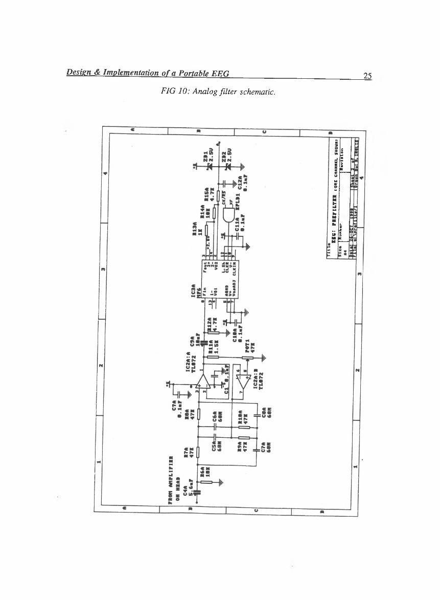
Design & Implementation of_a Portable EEG 25
FIG 10: Analog filter schematic.
IlCt P
IIFILTKI i
one c
hannel sh
ouhi
fHu"k
«r ~
rii
vi«t
»n—

Design & Implementation of_ a Portable EEG 26
3.4 Microcontroller Unit
The microcontroller unit is required to control the multiplexing of 4 channels,
perform real-time digital signal processing over the 4 channels, control/perform the
display of the output, and be able to communicate to other devices over an RS232 line,
whilst keeping size and power requirements at a minimum.
3.4.1 Microcontroller Selection
Digital signal processing algorithms are generally mathematically intensive. The
following benchmark table for floating point operations was compiled based on the cycle
periods and processing times supplied in the manufacturer’s specifications.
Processor Cvcle(ns) Ooeration Cvcles Time(us)
MC6805P3 1000 +,* 2000 2000-
MC6809 1000 +,* 2000 2000
MC68000 100 +,* 1000 100
TMS320C10 200 +,* 350 70
TMS320C20 200 +,* 300 60
TMS320C25 100 +,* 300 30
T414 50 + 230 11.5* 200 10
The Motorola MC6805P3 is commonly used in control applications, and includes
several dedicated features such as three I/O ports, a counter/timer, and on-chip EPROM.

The MC6809 is also available as part of a single board microcontroller. The three Texas
Instruments TMS320Cxx processors have instruction sets optimized for digital signal
processing, as well as other hardware features which enhance execution speed, as the
benchmark table shows. All three use a modified Harvard architecture with a partial
overlap of the instruction prefetch and execution, resulting in an effectively reduced cycle
time. The TMS320C2x chips both feature a combined multiply, accumulate operation.
The TMS320C25 also expands on the instruction set of the TMS320C20, with ’C20 code
being upwardly compatible. The Inmos T414 Transputer obained the best benchmark
performance, and offers the advantage of being able to increase performance by adding
transputers in a cellular network and by parallel decomposition of repetitive operations.
However, it is also the most expensive option, and offers performance greater than is
necessary.
The TMS320Cxx processors offer other advantages to those listed above. All are
excellently documented, and much software has been written fo r them. Also, they have
the added feature of a "powerdown" mode, in which they draw less current while
maintaining the current machine state, thus making them suitable for battery operation.
The TMS320C2x chips contain on-chip RAM, a counter/timer, and are easily interfaced
with memory and I/O, thus decreasing the amount of external hardware necessary.
Because of these factors, and its expanded instruction set, the TMS320C25 was chosen
as the basis for the microcontroller unit.
The TMS320C25 comes in a 68-pin grid-array package. In order to aid design and
hardware debugging, a "socket" was constructed which converted the 68-pin grid-array
to 68-pin dual-in-line, suitable for breadboarding. This socket also allowed each pin to
be labelled, and provided a contact for each pin which could be easily accessed with a
probe for a CRO or logic apfdyser. A logical pinout was devised, thus easing the
interface to the rest of the circuit. Some simple diagnostic-circuitry, described later in
this report, was also wired into the socket.
A block diagram of the microcontroller unit is given below. The schematic of the
TMS320C25 and the immediate system hardware appears on the page after.
Design & Implementation o f a Portable EEG______________________________ 27

FIG 11: Block diagram o f microcontroller.
Design & Implementation of_a Portable ___ 28
"TTTTa EEG: M I CROCONTROLLER5 l i •A4 N ur\ b ® r Dtuu ion
Bai s. JZZgj H Z iSKeet 2 0< 2L lIIl fct/ 1 --------- l-E.iayfl Tw; V. |4 l ] n

Design & Implementation of_a Portable 29
FIG 12: TMS320C25 and system hardware.
KK6:
M
ICB0
P10C
K88
0R

Design & Implementation of_ a Portable EEG 30
3.4.3 Memory
The on-board memory for the microcontroller appears over, and consists of 32K
x 16 bits of static data RAM, 32K x 16 bits of program RAM and 8K x 16 bits of
program ROM. All memory used is low power memory, in order to effectively
implement battery powered Operation. As these low-power memory ICs have access
times slower than the memory cycle time of the TMS320C25, a wait state must be
generated, and is described Jater in the report. Access times are 100ns for the RAM and
150ns for the ROM.
Although a wait state must be inserted for every external memory access, the
TMS320C25 provides a facility whereby 256 bytes of program memory may be
transferred into high-speed on-chip RAM and executed at full speed.
The memory circuit was also constructed on a wire-wrapped socket for ease of
breadboarding. The sockets for the TMS320C25 and the memory were constructed in
such a way that they needed only to be placed next to each other on the breadboard for
the data and address busses to connect This further enhanced the breadboarding and
debugging process by "hiding" almost 150 wires.

27
64
1
10
6£
?4
,,
I 2
76
4
Design & Implementation of_ a Portable EEG 31
FIG 13: Memory circuitry.
I*«:
HBIOIY CCT
Design & Implementation o fa Portable 32
3.4.4 I/O Decoding
When accessing its I/O space, the TMS320C25 places the address on pins A3-A0,
holding the other address lines low. This allows for the addressing of 16 peripherals.
The I/O address is decoded by a 74154. Half of a 7474 is used as a toggle flip flop for
the control of the filter clock and the RS232 port, denoted by the CK/RS line. Since both
the clock controlling the cut-off frequency of the low-pass filters, and the RS232 port,
must be interrupt driven and are both time sensitive, both use the External Flag (XF) pin
of the TMS320C25, as operations to this flag are faster than those to I/O or memory.
The CK/RS line allows the software to toggle the XF line between the filter clock and
the RS232 port. The. I/Q decoding was implemented on an EP900 Erasable
Programmable Logic Devicp.
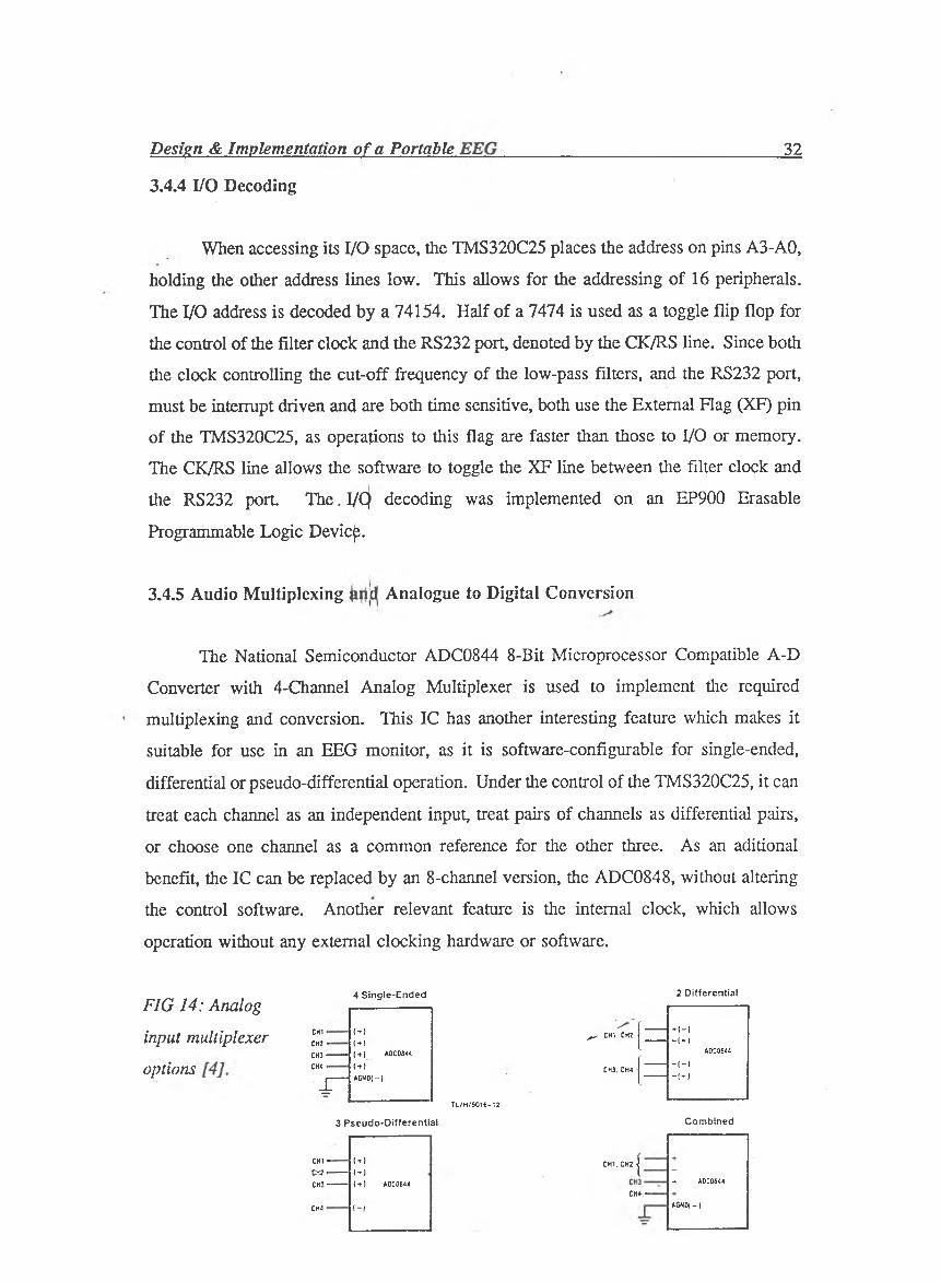
3.4.5 Audio Multiplexing Analogue to Digital Conversion
The National Semiconductor ADC0844 8-Bit Microprocessor Compatible A-D
Converter with 4-Channel Analog Multiplexer is used to implement the required
multiplexing and conversion. This IC has another interesting feature which makes it
suitable for use in an EEG monitor, as it is software-configurable for single-ended,
differential or pseudo-differential operation. Under the control of the TMS320C25, it can
treat each channel as an independent input, treat pairs of channels as differential pairs,
or choose one channel as a common reference for the other three. As an aditional
benefit, the IC can be replaced by an 8-channel version, the ADC0848, without altering
the control software. Another relevant feature is the internal clock, which allows
operation without any external clocking hardware or software.
FIG 14: Analog
input multiplexer
options [4
A Single-Ended 2 Differential
+ ( _ )cm 1 (-*■)(♦)( + ) ADC0844
^ CHI. CH2 ■ - ( * )CH2 -A0C0844CH3 — —
< + )4. | _ iCH4 ■ CH3. CH4 - \ f
r ~
AGNO(-) “ {•*■)
TL/H/50li-12
3 Pseudo-Differential Combined
CHI - ( -r) CHI. CH2 •!CHZ 1 --- (*•■)
{-(-) ADC08441
-t- ADC0S44CH3 ~— —CH4-:— ■
i — i ■ - - ACN0( - JCH<
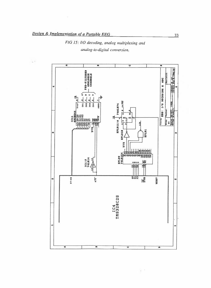
Design & Implementation ofji Portable EEG 33
FIG 15: HO decoding, analog multiplexing and
analog-to-digital conversion.
*«
«:
I'O
V
KC
0V
IM6
ft
A
»C
Runk*r
j KvT
aTon

Design & Implementation o f a Portable EEG 34
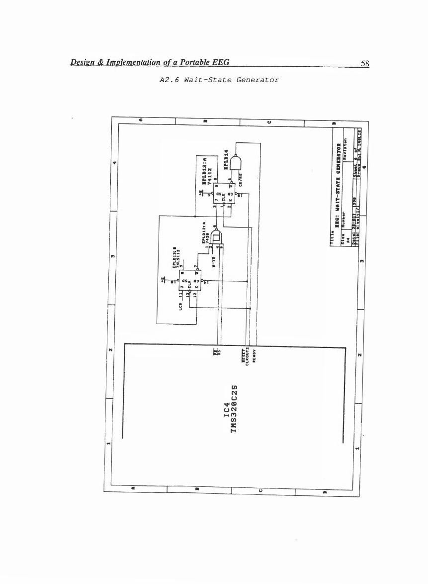
3.4.6 W ait State Generator
Both the memory ICs and the A-D converter have access times slower than the
memory cycle time of the TMS320C25 running at 20MHz. However, both are accessible
by the TMS320C25 with the insertion of 1 wait state. The display circuitry described in
section 3.4.8 of this report requires the insertion of 2 wait states to function correctly.
The circuit to supply these wait states, and an accompanying timing diagram,
appear on the following two pages.
The wait state generator was implemented on the EP900.
No wait states are requ|re4 when toggling the CK/RS line.

Design & Implementation of_a Portable EEG 35
FIG 16: Wait-state generator schematic.
Tin...
....
....
....
....
....
..KKC: M
AIT—8TATK
CINI1AT01
51*•
I b
unke
r 1d
ivis
ion

Design & Implementation of_ a Portable EEG 36
FIG 17: Wait-state generator timing diagram.
Y S 111 1 UAIT-STAT* nitlORV TWINSTrrrn M 1
| Hufikar1........."
TITTT 2 WAITSTATE TOUT TWINS~n"fi | M 1 j X«vIII«fl

Design & Implementation ofji Portable 37
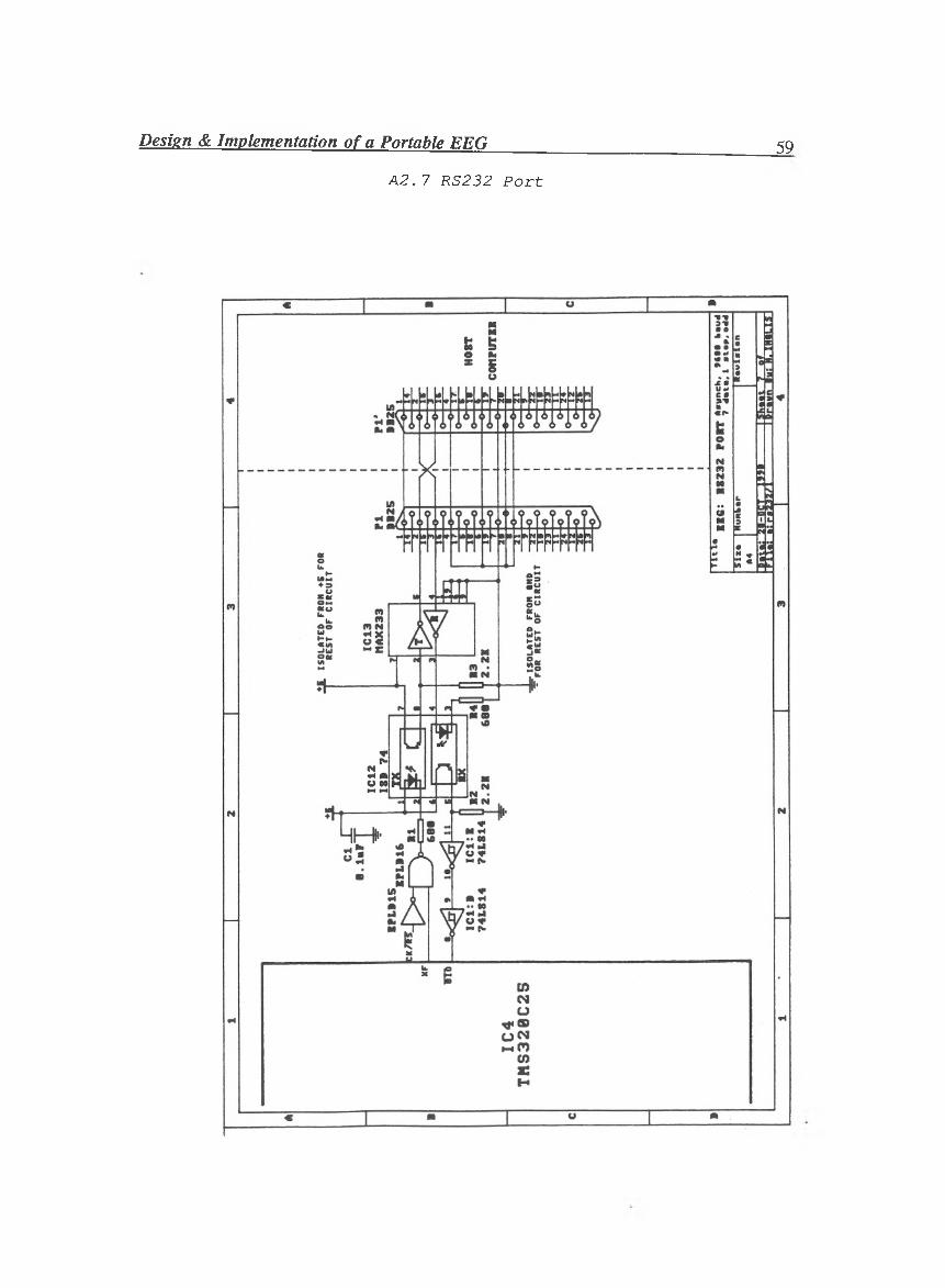
3.4.7 RS232 Port
In order to minimize on hardware, the RS232 port is implemented in software,
using the XF line and the polled interrupt line BIOZ. The port operates asynchronously
at 9600 baud, with 7 data bits, 1 stop bit and odd parity. The hardware is connected as
a null-modem, as no other RS232 control lines are implemented. The software for the
port appears in [5], entitled "An Implementation of a Software UART using the
TMS320C25".
Optoisolation is used to electrically isolate the EEG device from a device
connected via the RS232 port. This is to ensure the safety of the patient in the event of
an electrical fault in a device connected to this port.

Design & Implementation of_ a Portable EEG 38
FIG 18: RS232-portschematic.

Design & Implementation of_a Portable EEG 39
3.4.8 Display Circuitry
An aplhanumeric liquid crystal, display unit (LCD) is used as the output of the
unit. It can display two rows of 16 characters, and supports an extended ASCII character
set, as well as allowing eight user-programmable characters. With its own microprocessor
and memory, both the hardware and the software interfaces are simple to implement,
saving on both physical size and memory.
Included in the LCD’s character set are the Greek letters alpha, beta and theta.
Software was written to encode the Greek letter delta as one of the programmable
characters, thus allowing the unit to display the symbols for the four major brainwave
classes. Three more characters were programmed to implement bargraphs so that, for
example, the power present in each of the classes can be readily displayed in a graphical
form.

Design & Implementation of_a Portable EEG 40
FIG 19: Display circuit schematic.
LIQUI» CIVSTAL BISFLAV

Design & Implementation of_ a Portable EEG 41
4. SOFTWARE
4.1 Software Overview
Most of the software for the unit was written in a version of C, written by Texas
Instruments for their TMS320 range of microprocessors. It is similar to ANSI C, with
several additional features and several omissions. It is supplied with two libraries: a run
time support library and a floating-point library. The run-time support library provides
most of the necessary library functions defined in ANSI C, and the floating-point library
provides mathematical library functions using floating point arithmetic. A facility to edit
the libraries, as well as the source code for the run-time support library, was also
supplied. The remainder of the code was written in TMS320C25 assembly language.
The TMS320C25 incorporates a type of Harvard architecture, having separate data
and program memory addressing multiplexed over the one address bus. In order to aid
the design of the software, the program memory ROM was emulated using a ROM
Emulator module with a suitably equipped Arium Logic Analyser. While using this
module greatly facilitated program development (as opposed to repeatedly erasing and
reprogramming EPROMs), it constrained the size of the program memory to 8 K-Words.
Several steps were taken in order to keep the software within this limit.
- The run-time support library was edited and recompiled, keeping only the necessary
functions.
- Where possible, the compiled code for each object was streamlined after compilation.
- The code was written in a style which minimized program memory usage by avoiding •
macros, and writing a minimum number of functions in a very basic form. This was
done at the sacrifice of some structure and readability of code, which in some instances
resembles assembly language. Program documentation has been provided in the code
listings.

Design & Implementation of a Portable EEG 42
A further point to note concerning the software is that the functions for driving the
liquid crystal display and for driving the analog to digital converter have been written in
"pieces", to allow for the parallel operation of these devices. To expalin: In order to
write a character to the LCD, one must write one byte to the appropriate port, and wait
for 40 us for the LCD to be ready for the next character. In order to read a byte from
channel one of the A-D converter, one must write one byte to the appropriate port to
initiate the analog to digital conversion, wait for 40 us, then read a byte from the port.
In a strictly modular programming style, these functions would have been written in the
following form. The procedure Wait40usQ is assumed.
void printc(c) int c;
/* Prints data on LCD */ {_outport3 (c);Wait40us () ;}
int GetDataO
/* Gets ADC CHI data */ {_outport0( ini;)WaitAOus () ;return(_inport0 ());}
This code would create two high level abstractions, or objects, called printc() and
GetDataO, which would "hide" their implementational details from the programmer.
However, this modular programming style enforces sequential operation. The operations
of the LCD and the ADC, whilst being completely independent of each other, could not
occur concurrently.
Instead, the code has been written in a style similar to that used by several
"supercomputers", such as the MIPS machine [6], whereby independent operations can
occur concurrently, at the expense of code modularity. The above two functions are now
implemented as four function "pieces", printc(), SetCHl(), GetDataO and Wait40us().
Again, Wait40us() is assumed.

Design & Implementation of_a Portable EEG 43
void printc(c) /* Sends c to LCD */int c;
{_outport2(c);}
void Set CHI ()/* Initiates A-D conversion on channel 1 of ADC */{_outportO( i n i t _ c m d ) ;}
int GetData ()/* Gets converted data from ADC */{return (_inportO () ) ;}
The code to write to the LCD while converting incoming data is then as follows:
pri nt c( c h a r a c te r_;SetCHl () ; /*Wait40us () ;i=GetData () ;printc ( c h a r a c t e r_) ;
/* Sends character to LCD */Initiates A-D conversion */
/* Waits for both operations */ /* Gets the data from the ADC */ /* Sends next character to LCD */
This allows the two time consuming operations of input and output to occur,
simultaneously. This is very important in a real-time computing environment, where
events (eg. time-domain data sampling) must occur at regular intervals.s '
Several seemingly inexplicable problems were encountered while using the C
compiler and linker, involving pointers and external variables. After consultation with
a TI dealer and two other engineers who had used the TMS320 chips, it was discovered
that there are errors in the C compiler and linker themselves. These problems were
complicated by the nature of the TMS320 User’s Guide and the TI C Manual and
Assembler Manual. These were found to be hard to use, with most of the important
information being located by luck and accident. Several important facts involving the use
of the registers are "glossed over". In addition, the assembly language examples in the
User’s Guide were found to be misleading, in that they would only work under certain
circumstances which are not mentioned.
The above factors lead to code which completely avoids the use of pointers, and
minimizes use of the stack.
4.2 Module Overview
The software written for the device is implemented in the modules adcio.c, Icdio.c,
ffttms.c, teste , and timing.asm. Module adcio.c supplies function pieces to control the
analog to digital converter, allowing the programmer to set the various modes and obtain
the converted data. Similarly, module Icdio.c handles output to the liquid crystal display,
including display initialisation and the programming of custom graphics characters.
Module ffttms.c is an implementation of an in-place Cooley-Tukey 64 point Fast Fourier
Transform. The coordination of the above functions occurs in test.c, which is a program
to take time-domain input data from the analog to digital converter, convert it to
frequency domain power spectrum data via the FFT, group this data into the delta, theta,
alpha and beta brainwave classes, and output these to the liquid crystal display in the
form of four bar-graphs. Module timing.asm was written in assembly language, and
controls the timer interrupt which produces the clock signal to program the cut-off
frequency of the MF6 filter IC. The run-time support library had to be further edited in
order to support the timer interrupts.
Design & Implementation o£_ a Portable EEG____________________________________44
Listings of the software itself are included in this report as APPENDIX 3.

Design & Implementation of_a Portable EEG 45
5, PERFORMANCE
5.1 Active Electrode Performance
The active electrode system was found to perform very well. Movements of the
wires connecting the patient to the EEG machine had no noticeable effect on the display.
The unit and the patient were in a very electrically noisy environment, but seemed to
operate with no ill effects. No difference in the display was discemable when nearby
electrical activity was ceased (ie. other appliances in the room were switched off),
indicating that the active electrodes were reducing the effects of electrical noise.
5.2 Filter Performance
The analog filters employed were found to perform excellently, with only one
minor problem. One of the "twin-t" notch filters, whilst having a very steep notch,
unfortunately had the notch centered at 47 Hz instead of 50 Hz. Since 1% tolerance
resistors were used, it is almost certain that the wider-tolerance capacitors were causing
the notch to stray from the calculated value. This could have been corrected by using
narrow-tolerance capacitors, such as mylar or polystyrene capacitors. However, it was
found that the notch of the filter could be "widened" to attenuate 50 Hz, with only a
small loss of delta-wave signal appearing on the display.
5.3 Computer Hardware Performance
The computer hardware performed as expected. All of the "glue" logic, including
the wait-state generator and the I/O decoding circuitry, fitted comfortably on an EP900
Erasable Programmable Logic Device (EPLD). This resulted'in the computer being
implemented with only 6 IC’s: the TMS320C25, the EP900, two data RAM chips and
two program ROM chips, which were emulated with the Arium EPROM Emulator
module. The two program RAM chips were not used, but their sockets were wired to

Design & Implementation of_ a Portable EEG 46
allow for their insertion for system expansion.
No problems were encountered with clock skew or noise, even with four clock
signals present on the board. The TMS320C25 is driven by a 20 MHz crystal, using its
own internal oscillator to generate the signal. It then produces two 5 MHz signals,
CLKOUT1 and CLKOUT2, which drive the rest of the computer hardware. The final
clock signal comes from the EPLD, which has a frequency of 50 x fc for the MF6 filters.
All clocks showed no evidence of reflection or noise.
The unit was found to have a current consumption of ~119 mA while operational.
This is low enough to allow several hours ( <10 ) of operation using standard dry-cell
batteries and a voltage regulator supplying +/- 5V.
5.4 Computer Software Performance
Once all of the previously mentioned problems were overcome, most of the
software worked well. Even with the CPU running at half its maximum clock speed, and
with one wait-state memory, the EFT calculation seemed to complete in less than the time
taken for one half of a 64 Hz cycle — 7.8 ms. A more accurate time could not be
determined.
The only remaining problem with the software is the timer interrupt code. At low
frequencies, the timer interrupt causes no problems. However, when performing a 64*
point EFT, the MF6 filter requires an input clock frequency of 2 x 32 x 50 = 3.2kHz.
Problems were encountered at this frequency, with the computer sometimes "hanging".
Since all other aspects of the hardware work perfectly, and there is no noise trouble with
the 20 MHz and the two 5 MHz clock signals, it is strongly suspected that this problem
stems from the poor documentation of the operation of the- interrupts in the manuals.
There are possibly more faults in the TI C environment, especially since it was necessary
to write the interrupt code in assembler and edit the run-time support library to get the
interrupts to work at all.

Design & Implementation of_ a Portable A&
5.5 Overall System Performance
When using a sine-wave signal generator as input, the unit performed well in
determining the frequencies present.
A problem arose, however, which prevented the consistent operation of the unit
at the low-signal input levels required of an EEG machine. Once the EEG cables were
properly shielded and the active electrode circuitry was enclosed in a double-shielded box,
the amplifiers and filters were found to be immune to virtually all external sources of
electromagnetic interference. The amplifiers were capable of displaying brainwave
activity on an oscilliscope while the computer circuitry was turned off. However, high-
frequency "noise" on the power supply due to the operation of the computer degraded the
performance of the amplifier. Large decoupling capacitors and LC filters in the power
rails did not reduce this level of interference sufficiently. It is felt that this problem could
be solved by having separate voltage regulators and filters for the digital and analog
circuitry, but time did not permit their construction.
Another internal source of noise which seriously degraded the unit’s performance
until its discovery was the ROM emulator. This introduced noise into the system both
through the ROM connections and through the power supply. The final version of the
software was programmed into EPROMs to eliminate this problem.

Design & Implementation o f a Portable EEG 48
6. CONCLUSIONS
This project has been a serious study into the viability of both the portable EEG
monitor and the active electrode.
The system design has attempted to maintain generality and programmability in
all aspects.
The system has been designed to operate as a portable EEG monitor over four
channels, able to be operated outside an electromagnetically shielded environment. The
method of processing, the sampling frequency and all aspects of filtering are
programmable.
The estimated cost of the system of under $600 provides a cost effective
implementation of a portable EEG monitor.

Design & Implementation of_a Portable EEG 49
APPENDIX 1 Block Diagrams

Design & Implementation o£_a Portable 50
A l . l P o r t a b l e EEG Unit
EE
G:
BL
OC
K
DIA
GR
AM

Design & Implementation of_ a Portable EEG 51
A1.2 M i c r o c o n t r o l l e r
E E
G:
MIC
RO
CO
NT
RO
LL
ER

Design & Implementation of_ a Portable EEG 52
APPENDIX 2*
Circuit Schematics

Design & Implementation o f a Portable EEG 53
A2.1 A c t i v e E l e c t r o d e
TT
FIi
----
----
----
----
----
----
----
----
----
----
----
----
----
--B
IGs
AC
TIV
E
XU
CT
BO
BK
con
e cm
»nn
el s
ho
wn
)TI*» J Hu
nbar
fVivlslon---

Design & Implementation of_a Portable EEG 54
A 2.2 P r e f i l t e r i n g
U
M
plunbtr

IC1:A
||?
4L«
14
2
CIM
14
*!
■i
____
_ 39
«
Design & Implementation of_a Portable EEG 55
A 2.3 TMS320C25 System Hardware
tic:
mci
opio
ciss
oa

*TY-*V
Design & Implementation of_a Portable EEG 56
A2. 4 Memory
116:
MB10R
Y CCT

Design & Implementation o£_a Portable EEG 57
A2.5 I /O Decoding and A-D Conversion
•1311.
& a Portable EEG
1
1 I
N
I I
c
c
A2.6 Wait-State Generator
c
�N I �- I
• • i Ill OS� 0:1
I I .. � .. '
II ! I
I� '
�
I
I I I
�� = .. .. 0 c
lol � > "' u
u
u
•
•
.. a: .. "
.. = 10 I
.. ... c :I
...
N
Design & Implementation of_ a Portable EEG 59
A2.7 RS232 P o r t

Design & Implementation of_a Portable EEG 60
A2.8 D i s p l a y C i r c u i t r y
LIQIIIB CRYSTAL BISFLAY

Design & Implementation of_a Portable EEG 62
APPENDIX 3
Software Listings

Design & Implementation of_ a Portable EEG 63
/* MODULE adcio.c : I/O primitives for analog-to-digital converter */
extern void _outportO(); /* Import port 0 interface fh’s */
extern int _inportO();
#define DIFF12 0x00
#define DIFF21 0x01
#define DIFF34 0x02
#define DIFF43 0x03
#define CHI 0x04
#define CH2 0x05
#defme CH3 0x06
#define CH4 0x07
#define PD14 OxOC
#define PD24 OxOD
#define PD34 OxOE
/* Declare A-D conversion modes */
/* Differential modes */
/* Single-ended modes */
/* Pseudo-differential modes */
void SetDiffl2() { _outportO(DIFF12); } /* Set differential modes */
void SetDiff21() { _outportO(DIFF21); }
void SetDiff34() { _outportO(DIFF34); }
void SetDiff43() { _outportO(DIFF43); }
void SetCHl() {
void SetCH2() {
void SetCH3() {
void SetCH4() {
_outportO(CHl); }
_outportO(CH2); }
_outportO(CH3); }
_outportO(CH4); }
/* Set single-ended modes */
void SetPD14() { _outportO(PD14); } /* Set pseudo-differential modes*/
void SetPD24() { _outportO(PD24); }

Design & Implementation of a Portable EEG 64
void SetPD34() { _outportO(PD34); }
int GetDataO
{return (_inport0()%256);
}
/* Get the converted data */
/* The %256 is to strip the -*/
/* upper 8 bits */

Design & Implementation of_ a Portable EEG 65
/* MODULE lcdio.c : Output primitives for the liquid crystal display */
/* Control characters for the */
/* LCD screen... */
#defme CLEAR 0x01 /* Clears screen, cursor home */
#define HOME 0x02 /* Cursor home,screen unchanged */
#define LF OxCO /* Line feed */
#defme NrChrs 4 /* Number of programmable - */
#define NrRows NrChrs *8 /* - characters and rows used */
extern void Wait40us(),_outport2(), /* Declare global external fh’s */
_outport3();.
LCDInitO /* LCD initialisation routine */
{ /* Sends initialisation code &- */
int i; /*programmable character - */
int Code[6],CGData[32]; /*graphics (CG) information */
/* These arrays could not be initialised in the normal way as
/* done in K-R C, as Texas Instruments C does not support it
Code[0] = 0x38; /*Sets: 8-bit mode */
Code[l] = 0x38; l*2 lines */
Code[2] = 0x38; /* 5x7 pixel characters; */
Code[3] = 0x06; /* Cursor moves right */
Code[4] = OxOF; /* Flashing cursor */
Code[5] = 0x01; /* Clear display */
/* Data for a two bar character */
CGData[0] = 0x00; /* */
CGData[l] = OxlF;yy* ***** ^ */
CGData[2] = 0x00; /* */
CGData[3] = 0x00; /* */
CGData[4] = 0x00; /* */

Design & Imglementation o£_a Portable EEG 6 6
CGData[5] = OxlF; /* ***** */
CGData[6] = OxOO; /* */
CGData[7] = OxOO> /* */
/* Data for one (upper) bar */
CGData[8] = 0x00; /* */
CGData[9] = OxlF; /* ***** */
CGData[10] = 0x00; /* */
C G D ata[ll] = 0x00 */
CGData[12] = 0x00 1* */
CGData[13] = 0x00 */
CGData[14] = 0x00 */
CGData[15] = 0x00 */
/* Data for one (lower) bar */
CGData[16] = 0x00; /* */
CGData[17] = 0x00; /* */
CGData[18] = 0x00 /* */
CGData[19] = 0x00 */
CGData[20] = 0x00; /* */
CGData[21] = OxlF; /* ***** */
CGData[22] = 0x00; 1* • */
CGData[23] = 0x00; I* */
/* Data for the delta character */
CGData[24] = OxOF 1* */
CGData[25] = 0x08 * */
CGData[26] = 0x04 /* * */
CGData[27] = OxOE /* *** */
CGData[28] = O xll /* * % */
CGData[29] = O xll /* * * */
CGData[30] = OxOE /* *** */
CGData[31] = 0x00 /* */

Design & Implementation of a Portable EEG 61
for ( i=0 ; i<=400 ; i++ )
Wait40us();
for ( i=0 ; i<=5 ; i++ )
{_outport2(Code[i]);
Wait40us();
}for ( i=0 ; i<=400 ; i++ )
Wait40us();
• _outport2(0x40);
Wait40us();
for ( i=0 ; i<=63 ; i++ )
{_outport3(0);
Wait40us();
}_outport2(0x40);
Wait40us();
for ( i=0 ; i<=NrRows-l ; i++ )
{_outport3(CGData[i]);
Wait40us();
}
_outport2(0x80);
Wait40us();
}
void clear()
{_outport2(CLEAR);
/ * Wait for LCD to power up */
/* Send the initialisation code */
/* Pause after initialisation */
/* Set CG RAM address to start */
/* Clear the CG RAM */
.. ^
/* Set CG RAM address to start */
/* Sent the character data
/* Set DD RAM address to start */
/* Clear the display. */

Design & Implementation of_a Portable EEG 6 8
}
void homeO /* Send cursor home */
{_outport2(HOME);
}
void lf() /* Line feed */
{_outport2(LF);
}
void printc(c) I* Print character to LCD
int c;
{_outport3(c);
}
Design & Implementation of_ a Portable EEG 69
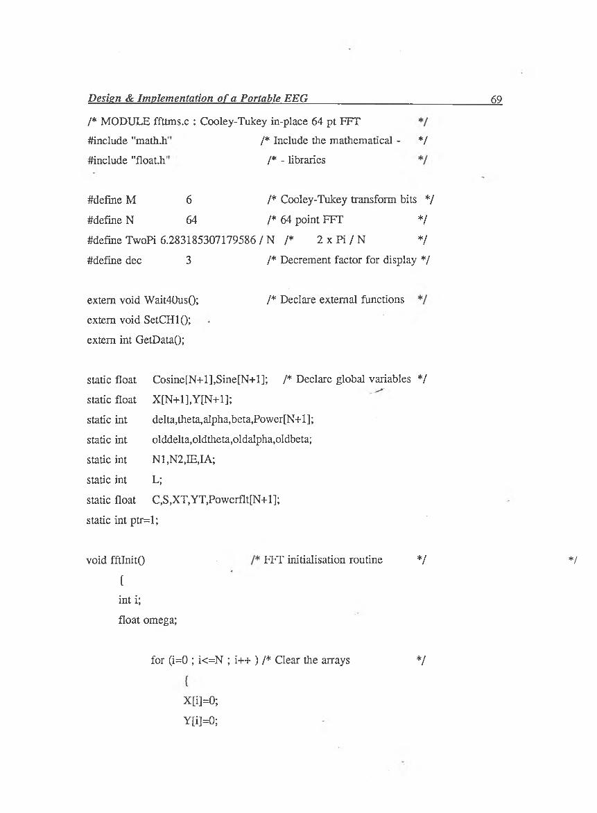
/* MODULE ffttms.c : Cooley-Tukey in-place 64 pt EFT
#include "math.h' /* Include the mathematical - */
#include "float.h' /* - libraries
#define M 6 /* Cooley-Tukey transform bits */
#define TwoPi 6.283185307179586 / N /*
#define N 64 /* 64 point FFT
N /* 2 x Pi / N
*/
*/
#defme dec 3 /* Decrement factor for display */
extern void Wait40us(); /* Declare external functions
extern void SetCHl();
extern int GetData();
static float Cosine[N+l],Sine[N+l]; /* Declare global variables */
static float X[N+1],Y[N+1];
static int delta,theta,alpha,beta,Power[N+l];
static int olddelta,oldtheta,oldalpha,oldbeta;
static int N1,N2,IE,IA;
static int L;
static float C,S,XT,YT,Powerflt[N+l];
static int ptr=l;
void fftlnit() /*FFT initialisation routine */
{int i;
float omega;
for (i=0 ; i<=N ; i++ ) /* Clear the arrays */

Design & Implementation of a Portable EEG 70
Power[i]=0;
}olddelta=6*dec; /* Initialise "old" values */
oldtheta=6*dec;
oldalpha=6*dec;
oldbeta=6*dec;
for ( i=l ; i<=N ; i++) / * Precalculating cos’s & sin’s */
{omega = TwoPi * (i-1);
Cosine[i] = .cos(omega);
Sine[i] = sin(omega);
}
}
void Readln() /* Gets data from ADC while printing */
{int i;
SetCHIO;
Wait40us();
X[ptr]=(float)GetData()/255;
Y[ptr++]=0;
if (ptr>64)
ptr=l;
for ( i=l ; i<=33 ; i++ )
Wait40us();
}
void fftO
{
/* Cooley-Tukey 64pt FFT */

Design & Implementation of_ a Portable EEG 71
extern void printc();
register int i,j;
int k,a;
N2=N; /* Cooley-Tukey algorithm */
for ( k=0 ; k<=M ; k++)
{N1=N2;
N2=N2/2;
IE=N/N1;
IA=1;
for ( j=l ; j<=N2 ; j++)
{C=Cosine[IA];
S=Sine[IA];
IA+=IE;
for ( i = j ; i<=N ; i+=Nl )
{L=i+N2;
XT=X[i]-X[L];
X[i]+=X[L];
YT=Y[i]-Y[L];
Y[i]+=Y[L];
X[L]=C*XT+S*YT;
Y[L]=C*YT-S*XT;
}
}
}
}
void UnscramO I* Unscramble output */

Design & Implementation o f a Portable EEG 72
{int i,j,k;
j= i;N1=N-1;
for ( i=l ; i<=Nl ; i++ )
{
if (i<j)
{
XT=X01;
■ X[j]=X[i ];
X[i]=XT;
XT=Y01;
Y[j]=Y[i];Y[i]=XT;
}
k=N/2;
while (k<j)
{j-=k;
k=k/2;
}
j+=k;
}
}
void WavesO /* Calculate the power present- */
{ /* -in each of the four - '•< */
int h,i; /* -brainwave classes */
for ( i=l ; i<=N ; i++ )

Design & Implementation o f a Portable EEG 73
{Powerflt[i]=2*sqrt( X[i]*X[i] + Y[i]*Y[i] );
Power[i]=(int)Powerflt[i];
}delta=(Power[2]+Power[3]+Power[4]+Power[5]);
theta= (Power [6]+Po wer [7 ] +Po wer [ 8 ]) *4/3;
alpha=(Power[9]+Power[10]+Power[ll]+Power[12]);
for ( h=13 ; h<=30 ; h++ )
beta+=Power[h];
beta=beta*4/18;
if ((delta>=12*dec) && (delta>=2*olddelta))
delta=olddelta;
if ((theta>=12*dec) && (theta>=2*oldtheta))
theta=oldtheta;. ^
if ((alpha>=12*dec) && (alpha>=2*oldalpha))
alpha=oldalpha;
if ((beta>=12*dec) && (beta>=2*oldbeta))
beta=oldbeta;
olddelta=delta;
oldtheta=theta;
oldalpha=alpha;
oldbeta=beta;
}
/* Write the bar graphs to LCD */
/* while getting data for next fft */
void ScreenDumpO
{int a;
extern void home(),lf();
home();
Wait40us();
/* Send cursor home */

Design & Implementation of_a Portable EEG 74
printc(0x03);
ReadlnQ;
/* Set printing going...
/* Simultaneously read data...
*/
*/
printc(0x2C);
ReadlnO;
printc(0xF2);
ReadlnO;
printc(0x3A);
ReadlnO;
for ( a=l ; a<=12 ; a-H-) /* Print the bars */
{if (delta>=dec)
{delta-=dec;
if (theta>=dec)
{printc(OxOO);
theta-=dec;
}else
printc(OxOl);
if (theta>=dec)
{printc(0x02);
theta-=dec;
}
else

Design & Implementation of_a Portable EEG 75
else
printc(0x20);
ReadlnO;
}
If();Wait40us();
printc(OxEO);
ReadlnO;
• printc(0x2C);
ReadlnO;
printc(0xE2);
ReadlnO;
printc(Ox3A);
ReadlnO;
for ( a=l ; a<=12 ; a++ )
{if (alpha>=dec)
{alpha-=dec;
if (beta>=dec)
{printc(0x00);
beta-=dec;
}
else
printc(OxOl);
}

Design & Implementation of_ a Portable EEG 76
else
if (beta>=dec)
printc(0x02);
beta-=dec;
}
else
printc(0x20);
ReadlnO;
}

77
/* MODULE test.c : controls operation of EEG device */
extern void fft()JJnscramO,WavesO,ScreenDumpO;
extern void SetCHl(); >.
void Wait40us() /* A pause for timing purposes */
{ int a;
for ( a=l ; a<=150 ; a+
+); }
Design & Implementation of a Portable _______________________
main()
{
extern void LCDInit(),fftInit();
int a;
LCDInitO;
fftlnitO;
while(l)
{ ScreenDump
O;
ScreenDumpO;
ffto;UnscramO;
Waves();
}
} .
/* Initialisations */
/* Get the data and print bars
/* Calculate transform */

78
/* MODULE timing.c : interrupt handler controlling the MF6 clock */
c_int4()
{int a;
asm(" SXF "); /* Sets the XF pin high */
for ( a=l ; a<=5 ; a++);
}
Design & Implementation of a Portable EEG______________________________

APPENDIX 4
References
[1] Scientific American, "THE BRAIN", Sept. 1979 Vol 241 No 3.
[2] Maher, "OPAMPS EXPLAINED", Federal Publishing Company
[3] National Semiconductor, "LINEAR DATABOOK 1", LM363 Notes
[4] National Semiconductor, "LINEAR DATABOOK 2", ADC0844, MF6 Notes
[5] Texas Instruments, "DIGITAL SIGNAL PROCESSING APPLICATIONS WITH
THE TMS320 FAMILY - THEORY, ALGORITHMS &
IMPLEMENTATIONS" Vol 2
- [6] Van De Goor, "COMPUTER ARCHITECTURE AND DESIGN", Addison-
Wesley, 1989
[7] Texas Instruments, "SECOND GENERATION TMS320 USER’S GUIDE"
[8] Texas Instruments, "TMS320Clx/TMS320C2x ASSEMBLY LANGUAGE
TOOLS"
[9] Texas Instruments, "TMS320C25 C COMPILER REFERENCE GUIDE"
[10] ETI, "TOP PROJECTS VOL.6", Federal Publishing Company
[11] Cromwell et al.,"BIOMEDICAL INSTRUMENTATION AND
MEASUREMENTS", Prentice Hall, 1973
[12] Tompkins, Webster, "DESIGN OF MICROCOMPUTER-BASED MEDICAL
INSTRUMENTATION", Prentice Hall, 1981
[13] Gevins, Reimond, "METHODS OF ANALYSIS OF BRAIN ELECTRICAL
AND MAGNETIC SIGNALS", EEG Handbook (Revised Series Vol 1), Elsener
Science Publishers, 1987
[14] Frost, "MIMETIC TECHNIQUES", EEG Handbook (Revised Series Vol 1),
Elsener Science Publishers, 1987.
[15] Council on Physical Medicine of the American Medical Association "MINIMAL
REQUIREMENTS OF THE AMERICAN MEDICAL ASSOCIATION FOR
ACCEPTABLE DIRECT-READING ELECTROENCEPHALOGRAPHS", Journal
of the American Medical Association Vol 138, No 13, 1948
Design & Implementation o f _ a Portable EE