deschler et al 2014 journal of physical chemistry letters.pdf
TRANSCRIPT

High Photoluminescence Efficiency and Optically Pumped Lasing inSolution-Processed Mixed Halide Perovskite SemiconductorsFelix Deschler,†,§ Michael Price,†,§ Sandeep Pathak,†,‡ Lina E. Klintberg,† David-Dominik Jarausch,†
Ruben Higler,† Sven Huttner,† Tomas Leijtens,‡ Samuel D. Stranks,‡ Henry J. Snaith,*,‡ Mete Atature,†
Richard T. Phillips,† and Richard H. Friend*,†
†Cavendish Laboratory, JJ Thomson Avenue, Cambridge CB3 0HE, United Kingdom‡Clarendon Laboratory, Parks Road, Oxford OX1 3PU, United Kingdom
*S Supporting Information
ABSTRACT: The study of the photophysical properties of organic−metallic lead halideperovskites, which demonstrate excellent photovoltaic performance in devices with electron-and hole-accepting layers, helps to understand their charge photogeneration andrecombination mechanism and unravels their potential for other optoelectronic applications.We report surprisingly high photoluminescence (PL) quantum efficiencies, up to 70%, inthese solution-processed crystalline films. We find that photoexcitation in the pristineCH3NH3PbI3−xClx perovskite results in free charge carrier formation within 1 ps and thatthese free charge carriers undergo bimolecular recombination on time scales of 10s to 100sof ns. To exemplify the high luminescence yield of the CH3NH3PbI3−xClx perovskite, weconstruct and demonstrate the operation of an optically pumped vertical cavity lasercomprising a layer of perovskite between a dielectric mirror and evaporated gold topmirrors. These long carrier lifetimes together with exceptionally high luminescence yield areunprecedented in such simply prepared inorganic semiconductors, and we note that theseproperties are ideally suited for photovoltaic diode operation.
SECTION: Energy Conversion and Storage; Energy and Charge Transport
Organo−lead mixed halide perovskite-based solar cellshave shown a breakthrough in power conversion
efficiency.1 Solution-processed devices with power conversionefficiencies of 10−12%2−6 were reported in 2012 and havemore recently exceeded 15% in devices processed byevaporation7 and sequential deposition.8 There is evidencefrom optical studies9,10 that the diffusion range for thephotoexcitations can be substantial, up to 1 μm, and thisallows efficient light harvesting across the thickness of theperovskite layer (typically 400 nm). Nevertheless, it has notbeen clear whether the mobile species is a neutral exciton orfree charge, nor is the origin of the high open-circuit voltagesclear. As was shown by Lee et al.,6 the mixed halide perovskiteis capable of both electron and hole charge conduction,consistent with the excellent performance of evaporated planarheterojunction structures reported by Liu et al.7 It was alsodemonstrated by Burschka et al.8 that the triiodide perovskite isan efficient sensitizer and can even operate as a hole conductor,sustaining reasonable efficiencies without a hole-acceptorlayer.11 Two-dimensional layer structures with PbIx layersseparated by organic ligands have been extensively investigatedby Mitzi et al. and show luminescent properties with excitoniccharacter.12−16 However, the perovskites used in the presentstudy are three-dimensional semiconductors. A fundamentalquestion is whether the photoexcitation in the perovskiteremains as a bound exciton and is later ionized at the electron-
and/or hole-accepting heterojunctions (either distributed orplanar) or whether charge generation occurs in the pristineperovskite material. In order to address this and also to studythe long-time recombination/luminescent processes, we carriedout transient photoluminescence (PL) and transient absorption(TA) measurements on spin-coated perovskite films spin-castonto glass substrates and also of working devices comprisingmixed halide perovskite on a compact titanium dioxideelectron-accepting electrode with a hole-acceptor layer formedby spin-coating the hole transporter 2,20,7,70-tetrakis(N,N-di-p-methoxyphenylamine)9,90-spirobifluorene (spiro-MeO-TAD).For sample preparation, methylamine (CH3NH2) solution
(33 wt %) in absolute ethanol was reacted with hydroiodic acid(HI, 57 wt %) in water with excess CH3NH2 under nitrogenatmosphere in ethanol at room temperature. Typical quantitieswere 24 mL of CH3NH2, 10 mL of HI, and 100 mL of ethanol.Crystallization of methylammonium iodide (CH3NH3I) wasachieved using a rotary evaporator; a white-colored powder wasformed, indicating successful crystallization. CH3NH3I andlead(II) chloride (PbCl2) were dissolved in anhydrous N,N-dimethylformamide at a 3:1 molar ratio of CH3NH3I to PbCl2
Received: March 14, 2014Accepted: March 24, 2014Published: March 24, 2014
Letter
pubs.acs.org/JPCL
© 2014 American Chemical Society 1421 dx.doi.org/10.1021/jz5005285 | J. Phys. Chem. Lett. 2014, 5, 1421−1426
This is an open access article published under a Creative Commons Attribution (CC-BY)License, which permits unrestricted use, distribution and reproduction in any medium,provided the author and source are cited.

to produce a mixed halide perovskite precursor solution. Thinfilm samples were prepared by spin-coating followed byannealing on a hot plate at 100 °C for 60 min (full detailsare given in the Supporting Information (SI)).PL from these materials is emitted in a relatively narrow band
centered at 1.6 eV, just below the absorption edge, as shown inFigure S1 (SI). Figure 1a shows the photoluminescencequantum efficiency (PLQE) as a function of excitation fluencefor a thin perovskite film on glass.The PLQE is relatively low at low fluences (<25 mW/cm2)
but rises rapidly above 50% (by 100 mW/cm2) and reaches amaximum value of 70% at high excitation densities. This isremarkably high and indicates few nonradiative decay pathways.We consider the lower PLQE at low excitation fluence to bedue to the presence of defects through which nonradiativedecay can occur. Radiative recombination becomes dominantover recombination at high fluences after the defects are filled.The rise in the PLQE toward higher fluences suggests anexcitation-density-dependent radiative recombination. We notethat comparable PL efficiencies are rarely achieved in untreatedinorganic or hybrid materials; thus, nanocrystalline II−VIsemiconductors show PL efficiencies of below 15% withoutspecial core−shell features, and bulk systems used in solar cellssuch as copper indium gallium selenide show lowerefficiencies.17−19 It is therefore extremely unusual to find suchhigh PL efficiency, and we consider that this points to a highsemiconducting quality and overall low defect density of thespincoated perovskite materials.We studied the recombination behavior of the photo-
excitations in films and solar cells with TA and transient PLspectroscopy on nanosecond time scales to track the excitationdensity and recombination rate, respectively. Working solarcells based on CH3NH3PbI3−xClx perovskites were fabricatedwith the structure as shown in the inset in Figure S2 (SI). Thecells were composed of a thin compact TiO2 layer (50 nm)deposited on an FTO covered glass substrate followed by a thin(300 nm) mesoporous Al2O3 layer onto which theCH3NH3PbI3−xClx was deposited by spin-coating.3,20 Thisstructure was capped with a spiro-MeOTAD layer acting as thehole acceptor and gold electrodes for charge extraction. Beforetaking TA measurements (details of the laser setup are given inthe SI), the power conversion efficiencies of the solar cells weremeasured in a solar simulator under AM1.5 conditions, yieldingvalues around ∼10% (Figure S3, SI). All measurements wereperformed at <10 μJ/cm2, which falls within the linearexcitation fluence regime, as verified by a linear response ofthe TA signal (at zero delay time) and external quantumefficiency (EQE) of the devices up to fluences of 50 μJ/cm2. Attimes beyond 1 ps, the TA response shows a ground-statebleaching (GSB) response peaked at 1.65 eV that is spectrallyunchanged out to times beyond 200 ns, as shown in Figure S2(SI). For comparison, Figure S1 (SI) shows the linearabsorption and PL spectrum. Any spectral signature due tothe spiro-MeOTAD is concealed by the strong perovskitesignal, and we consider that the GSB feature at 1.65 eV can beused to track the photoexcitation density as a function of time.We also measured the transient PL of working devices underopen-circuit conditions and also of thin films. PL excitation wasperformed at 2.3 eV with fluences in the range of 2−10 μJ/cm2.The PL (see Figure S1, SI) showed no detectable spectralevolution with time. At high fluences, we observed a blue shiftof the steady-state PL spectrum, by about 50 meV, and abroadening toward higher energies, which indicates state filling
of the band structure and emission from higher-lying states21
(Figure S4, SI). We calculated the expected shift in the PLspectrum from the photoexcitation density (ρexc ≈ 1020/cm3),
Figure 1. (a) PLQE of CH3NH3PbI3−xClx films on spectrosil,annealed in air and capped with a thin PMMA layer. Excitation wasperformed with a cw laser at 2.33 eV. The integrated PL intensity wastaken from 1.77 to 1.46 eV, measured in a Labsphere integratingsphere. The increase in PLQE with excitation fluence indicates acompetition between bimolecular recombination and monomolecular,trap-assisted charge recombination. The high values shown heredemonstrate that at higher fluences, the dominant mechanism ofrecombination is radiative. (b) Plot of the normalized PL intensity(integrated from 1.71 to 1.57 eV) and the TA signal versus time for aworking device and film samples. Excitation for PL decays of films anddevices was performed with a pulsed laser at 2.3 eV and fluence of ∼2μJ/cm2. The pulse length was 100 fs and 400 ps for devices and films,respectively. For TA measurements, the device was held at open circuitin a nitrogen-filled holder and was photoexcited at 2.33 eV (10 μJ/cm2, pulse length 400 ps). The excitation fluence for films was 2 μJ/cm2. (c) Plot of the normalized PL intensity (integrated from 1.71 to1.57 eV) versus the square of the TA signal for the samples shown in(b).
The Journal of Physical Chemistry Letters Letter
dx.doi.org/10.1021/jz5005285 | J. Phys. Chem. Lett. 2014, 5, 1421−14261422
the crystal unit size volume6 (V ≈ 10−21 cm3), and the densityof states22 (g ≈ 5/eV). We found a calculated shift of ∼20 meV,which is consistent with the observed shift of ∼50 meV and inagreement with previous observations of radiative free carrierrecombination in III−V semiconductors.21
Figure 1b shows the comparison between the normalizeddecays of the GSB feature at 1.65 eV and the spectrallyintegrated PL centered at 1.6 eV.We find a faster decay of the PL than of the TA. We note
that the PL decay reported at low fluences9,10 is approximatelymonoexponential (see also Figure S5, SI), but at the higherfluences used here, comparable to those for the TA and onlyslightly above solar illumination conditions, neither the PL northe TA can be described by such a monomolecular exponentialdecay. The solid lines in Figure 1b are fits of the TA decays to asimple bimolecular decay response
=+ ·
f ta b t
( )1
The film shows the slower decay and is well modeled by thisbimolecular rate out to 1 μs. The device shows faster decaysthat are modeled by this bimolecular rate only at early times.The solid lines in Figure 1b are fits for bimolecular rates of 7.4× 10⁻¹¹ (film) and 7.3 × 10⁻¹¹ cm3 s−1 (device). This value isvery close to bimolecular rate constants determined fromterahertz measurements of the loss of mobile charge carriers,23
confirming that the observed PL arises predominantly fromcharge recombination for films. We note as a comment thatfilms prepared fully under nitrogen conditions show fasterkinetics due to intrinsic effects that are reduced when thesample is prepared in ambient conditions (Figure S6, SI).Figure 1c shows the data of Figure 1b plotted as the
normalized PL kinetics versus the square of the absolute GSBkinetics (with time as the implicit variable).The PL is proportional to the square of the TA for all
samples measured, indicating that the PL emission rate isproportional to the square of the excitation density or theproduct of the electron and hole concentrations (equal foruncontacted films). It is interesting to note that thisrelationship is observed for films as well as devices that showvery different absolute decay rates (see Figure 1b) and differentPL strengths. This indicates that, besides charge extraction,mixed halide perovskites show few other nonradiative decaychannels in photovoltaic devices, a prerequisite for efficientphotovoltaic performance.24 These results indicate thatluminescence in organo−lead mixed halide perovskitesCH3NH3PbI3−xClx results from bimolecular free carrierelectron−hole recombination and highlight the surprisinglyhigh semiconducting quality of these spin-coated anddisordered materials.The evolution of charge generation following photoexcitation
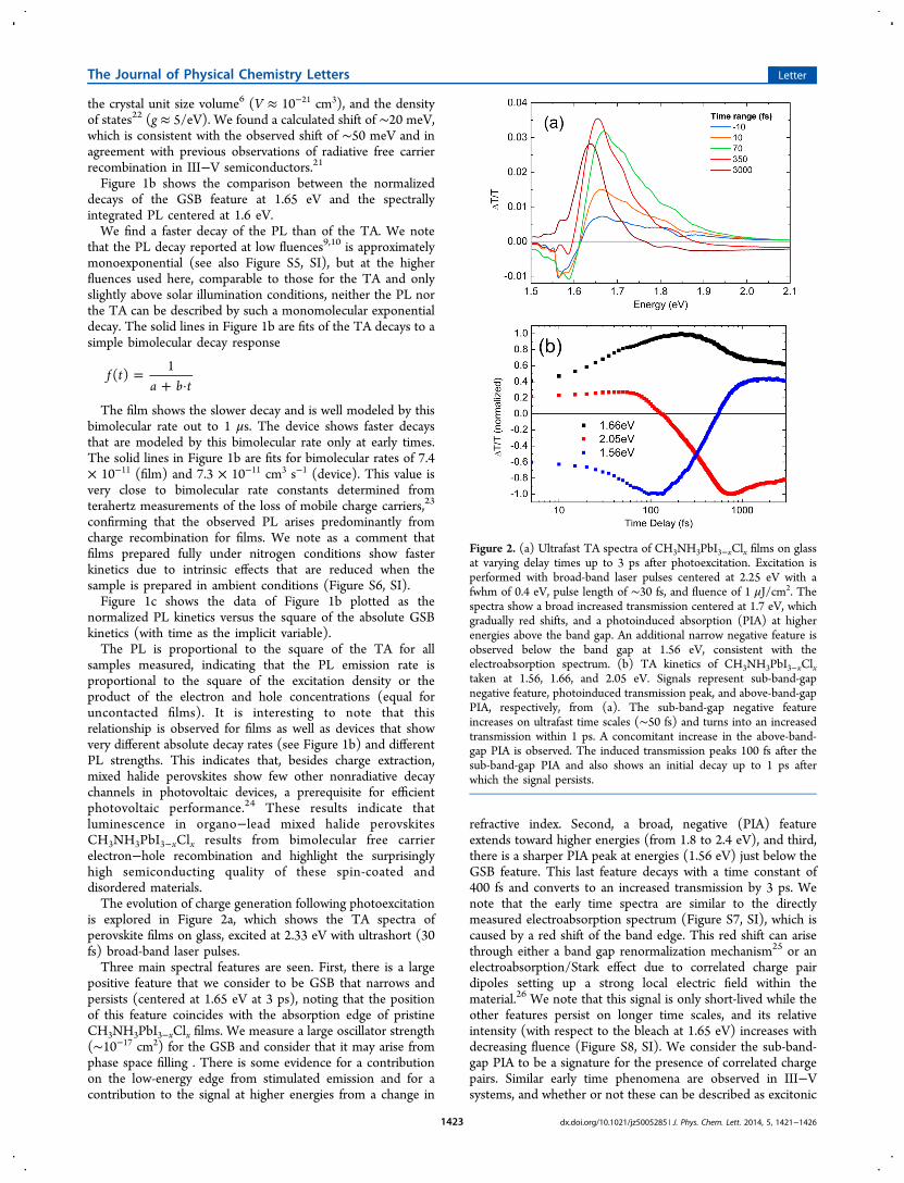
is explored in Figure 2a, which shows the TA spectra ofperovskite films on glass, excited at 2.33 eV with ultrashort (30fs) broad-band laser pulses.Three main spectral features are seen. First, there is a large
positive feature that we consider to be GSB that narrows andpersists (centered at 1.65 eV at 3 ps), noting that the positionof this feature coincides with the absorption edge of pristineCH3NH3PbI3−xClx films. We measure a large oscillator strength(∼10−17 cm2) for the GSB and consider that it may arise fromphase space filling . There is some evidence for a contributionon the low-energy edge from stimulated emission and for acontribution to the signal at higher energies from a change in
refractive index. Second, a broad, negative (PIA) featureextends toward higher energies (from 1.8 to 2.4 eV), and third,there is a sharper PIA peak at energies (1.56 eV) just below theGSB feature. This last feature decays with a time constant of400 fs and converts to an increased transmission by 3 ps. Wenote that the early time spectra are similar to the directlymeasured electroabsorption spectrum (Figure S7, SI), which iscaused by a red shift of the band edge. This red shift can arisethrough either a band gap renormalization mechanism25 or anelectroabsorption/Stark effect due to correlated charge pairdipoles setting up a strong local electric field within thematerial.26 We note that this signal is only short-lived while theother features persist on longer time scales, and its relativeintensity (with respect to the bleach at 1.65 eV) increases withdecreasing fluence (Figure S8, SI). We consider the sub-band-gap PIA to be a signature for the presence of correlated chargepairs. Similar early time phenomena are observed in III−Vsystems, and whether or not these can be described as excitonic
Figure 2. (a) Ultrafast TA spectra of CH3NH3PbI3−xClx films on glassat varying delay times up to 3 ps after photoexcitation. Excitation isperformed with broad-band laser pulses centered at 2.25 eV with afwhm of 0.4 eV, pulse length of ∼30 fs, and fluence of 1 μJ/cm2. Thespectra show a broad increased transmission centered at 1.7 eV, whichgradually red shifts, and a photoinduced absorption (PIA) at higherenergies above the band gap. An additional narrow negative feature isobserved below the band gap at 1.56 eV, consistent with theelectroabsorption spectrum. (b) TA kinetics of CH3NH3PbI3−xClxtaken at 1.56, 1.66, and 2.05 eV. Signals represent sub-band-gapnegative feature, photoinduced transmission peak, and above-band-gapPIA, respectively, from (a). The sub-band-gap negative featureincreases on ultrafast time scales (∼50 fs) and turns into an increasedtransmission within 1 ps. A concomitant increase in the above-band-gap PIA is observed. The induced transmission peaks 100 fs after thesub-band-gap PIA and also shows an initial decay up to 1 ps afterwhich the signal persists.
The Journal of Physical Chemistry Letters Letter
dx.doi.org/10.1021/jz5005285 | J. Phys. Chem. Lett. 2014, 5, 1421−14261423

populations is actively debated.27,28 Figure 2b shows the kinetictraces of the main features.The rise in the broad PIA signal (2.05 eV) is correlated with
the decay of the PIA feature at 1.56 eV, and on that same timescale, there is an enhancement in the GSB at 1.65 eV. Theresponse then remains constant after 900 fs, out to times aslong as microseconds9 (Figure S1, SI). The early time spectrumis consistent with the presence of correlated charge pairs, andthe observed loss of this signal within a subpicosecond is similarto the time scale of phonon-driven ionization observed in III−Vsystems.25 We therefore assign the later time spectrum to thatof free charges, which are formed within 1 ps afterphotoexcitation. This assignment is further supported by thecorrelation between the kinetics of this feature at longer timesand current extraction transients measured in devices (FigureS9, SI).As a test of the high photophysical quality of the
CH3NH3PbI3−xClx perovskite semiconductors, we have con-structed a vertical cavity optical structure in which a perovskitefilm is sandwiched between a gold mirror and a standarddielectric stack mirror29 with a reflectance band from 1.77 eV(see the SI for details on fabrication and measurement). Laserexcitation at 2.33 eV with 0.4 ns duration pulses reveals the
presence of cavity modes spaced by about 9.5 THz, as shown inFigure 3a.Above a threshold of 0.2 μJ/pulse, we observe an order of
magnitude increase in the slope of the output curve (Figure3b), line narrowing (Figure S10, SI), and the intensity beingtransferred to the mode closest to the PL emission peak.At high fluences, we also observe amplified spontaneous
emission (ASE) in thin films (Figure S11, SI), with asignificantly broader spectral width compared to the cavitymodes. The faster cavity ring down time of the lasing modecompared to the side bands, of order 5 ns, can be seen in FigureS12. Pulsed intensity correlation measurements (Figure 3c andS13) show photon bunching at zero time delay for lowexcitation densities below the lasing threshold, which isconsistent with amplified spontaneous emission. In contrast,similar measurements under high excitation densities (Figure3d) show a strong suppression of photon bunching, whichmanifests the high coherence of the emission and thereforelasing. In comparison with previous reports in two-dimensionalperovskite systems,30 we observe lasing at room temperatureand do not find a pronounced shift in the PL spectrumcompared to low fluences, which rules out previously observedbiexcitonic effects.
Figure 3. (a) Emission spectrum of a vertical microcavity with the structure as shown in the inset using a perovskite film as the gain medium. Thethickness of the perovskite layer was around 500 nm, and it was around 1 μm for the PMMA layer. Excitation was performed with a pulsed laser (400ps) at 2.33 eV and fluences as stated. At low fluences, three modes are resonant in the cavity with a mode spacing of ∼9.5 THz. At sufficiently highfluences, the mode at 1.6 eV is amplified. (b) Correlation between the intensity of the 1.6 eV mode and the pump laser energy showing a lasingthreshold at around 0.2 μJ/pulse. (c,d) Intensity correlation measurements of the cavity emission under excitation with 2.33 eV pulses (pulse widthof 68 ps, repetition rate of 80 MHz) selectively probing the lasing mode. The positions for zero time delay (red diamond) and the following laserpulses (black diamonds) are indicated. The blue line gives the average peak height, excluding the peak at zero time delay. The yellow area shows the4σ range. At low fluences (c) a pronounced correlation at zero time delay is found, which indicates photon bunching. At fluences above the lasingthreshold (d) the photon bunching effect vanishes, indicating lasing.
The Journal of Physical Chemistry Letters Letter
dx.doi.org/10.1021/jz5005285 | J. Phys. Chem. Lett. 2014, 5, 1421−14261424

In summary, we find a very unusual set of characteristics forthe mixed halide perovskite CH3NH3PbI3−xClx that indicatesurprisingly clean semiconducting behavior and give excellentPV performance. Free charges are formed within 1 ps ofphotoexcitation at room temperature and are long-lived, with abimolecular decay that gives rise to remarkably efficient PL,particularly at high excitation densities. This indicates thatmultiple electron−hole collisions can occur within the samplewithout nonradiative decay. This is a necessary criterion forphotovoltaic operation close to the Shockley−Queisser limit,24indicating significant future scope for these perovskite solarcells to reach the very highest solar power conversionefficiencies. The high room-temperature PLQE also revealsthe potential to use this class of three-dimensional perovskitesemiconductors in light-emitting devices because they provideeasy injection and transport of both electrons and holes,together with very high luminescence efficiency. These are theproperties required for LEDs and injection lasers.
■ ASSOCIATED CONTENT*S Supporting InformationAdditional figures, including steady-state absorption and PLspectra, TA spectra of photovoltaic devices, current−voltagecharacteristics of the photovoltaic devices, fluence-dependentPL spectra and kinetics, EA spectra, fluence-dependent TA offilms, line-narrowing of the cavity emission, and details ofsample fabrication, laser setup, and lasing measurements. Thismaterial is available free of charge via the Internet at http://pubs.acs.org.
■ AUTHOR INFORMATIONCorresponding Authors*E-mail: [email protected] (R.H.F.).*E-mail: [email protected] (H.J.S.).
Author Contributions§F.D. and M.P. contributed equally.
NotesThe authors declare no competing financial interest.
■ ACKNOWLEDGMENTSWe thank Dr. Cheng Li and Dr. Dan Credgington for assistancewith and helpful discussions on the EA measurements. Wethank the Engineering and Physical Sciences Research Council,and the Winton Programme (Cambridge) for the Physics ofSustainability for funding. M.P. wants to thank the CambridgeCommonwealth Trust and the Rutherford Foundation of NewZealand for funding.
■ REFERENCES(1) Snaith, H. J. Perovskites: The Emergence of a New Era for Low-Cost, High-Efficiency Solar Cells. J. Phys. Chem. Lett. 2013, 4, 3623−3630.(2) Abrusci, A.; Stranks, S. D.; Docampo, P.; Yip, H.-L.; Jen, A. K. Y.;Snaith, H. J. High-Performance Perovskite−Polymer Hybrid SolarCells via Electronic Coupling with Fullerene Monolayers. Nano Lett.2013, 13, 3124−3128.(3) Ball, J. M.; Lee, M. M.; Hey, A.; Snaith, H. J. Low-TemperatureProcessed Meso-Superstructured to Thin-Film Perovskite Solar Cells.Energy Environ. Sci. 2013, 6, 1739−1743.(4) Heo, J. H.; Im, S. H.; Noh, J. H.; Mandal, T. N.; Lim, C.-S.;Chang, J. A.; Lee, Y. H.; Kim, H.-j.; Sarkar, A.; Nazeeruddin, Md. K.;et al. Efficient Inorganic−Organic Hybrid Heterojunction Solar Cells
Containing Perovskite Compound and Polymeric Hole Conductors.Nat. Photonics 2013, 7, 486−491.(5) Kim, H. S.; Lee, C. R.; Im, J. H.; Lee, K. B.; Moehl, T.;Marchioro, A.; Moon, S. J.; Humphry-Baker, R.; Yum, J. H.; Moser, J.E.; et al. Lead Iodide Perovskite Sensitized All-Solid-State SubmicronThin Film Mesoscopic Solar Cell with Efficiency Exceeding 9%. Sci.Rep. 2012, 2, 591−598.(6) Lee, M. M.; Teuscher, J.; Miyasaka, T.; Murakami, T. N.; Snaith,H. J. Efficient Hybrid Solar Cells Based on Meso-SuperstructuredOrganometal Halide Perovskites. Science 2012, 338, 643−647.(7) Liu, M.; Johnston, M. B.; Snaith, H. J. Efficient PlanarHeterojunction Perovskite Solar Cells by Vapour Deposition. Nature2013, 501, 395−398.(8) Burschka, J.; Pellet, N.; Moon, S.-J.; Humphry-Baker, R.; Gao, P.;Nazeeruddin, Md. K.; Gratzel, M. Sequential Deposition as a Route toHigh-Performance Perovskite-Sensitized Solar Cells. Nature 2013,499, 316−319.(9) Stranks, S. D.; Eperon, G. E.; Grancini, G.; Menelaou, C.;Alcocer, M. J. P.; Leijtens, T.; Herz, L. M.; Petrozza, A.; Snaith, H. J.Electron−Hole Diffusion Lengths Exceeding 1 Micrometer in anOrganometal Trihalide Perovskite Absorber. Science 2013, 342, 341−344.(10) Xing, G.; Mathews, N.; Sun, S.; Lim, S. S.; Lam, Y. M.; Gratzel,M.; Mhaisalkar, S.; Sum, T. C. Long-Range Balanced Electron- andHole-Transport Lengths in Organic−Inorganic CH3NH3PBI3. Science2013, 342, 344−347.(11) Etgar, L.; Gao, P.; Xue, Z.; Peng, Q.; Chandiran, A. K.; Liu, B.;Nazeeruddin, Md. K.; Gratzel, M. Mesoscopic CH3NH3PBI3/TiO2
Heterojunction Solar Cells. J. Am. Chem. Soc. 2012, 134, 17396−17399.(12) Era, M.; Morimoto, S.; Tsutsui, T.; Saito, S. Organic−InorganicHeterostructure Electroluminescent Device Using a Layered Perov-skite Semiconductor (C6H5C2H4NH3)2PBI4. Appl. Phys. Lett. 1994, 65,676−678.(13) Kitazawa, N.; Watanabe, Y.; Nakamura, Y. Optical Properties ofCH3NH3PBX3 (X = Halogen) and Their Mixed-Halide Crystals. J.Mater. Sci. 2002, 37, 3585−3587.(14) Ishihara, T. Optical Properties of PBI-Based PerovskiteStructures. J. Lumin. 1994, 60−61, 269−274.(15) Mitzi, D. B. Synthesis, Structure, and Properties of Organic-Inorganic Perovskites and Related Materials. In Progress in InorganicChemistry; Karlin, K. D., Ed.; John Wiley & Sons, Inc.: New York,2007; pp 1−121.(16) Mitzi, D. B.; Wang, S.; Feild, C. A.; Chess, C. A.; Guloy, A. M.Conducting Layered Organic−Inorganic Halides Containing ⟨110⟩-Oriented Perovskite Sheets. Science 1995, 267, 1473−1476.(17) Talapin, D. V.; Rogach, A. L.; Shevchenko, E. V.; Kornowski, A.;Haase, M.; Weller, H. Dynamic Distribution of Growth Rates withinthe Ensembles of Colloidal II−VI and III−V SemiconductorNanocrystals as a Factor Governing Their PhotoluminescenceEfficiency. J. Am. Chem. Soc. 2002, 124, 5782−5790.(18) Dabbousi, B. O.; Rodriguez-Viejo, J.; Mikulec, F. V.; Heine, J.R.; Mattoussi, H.; Ober, R.; Jensen, K. F.; Bawendi, M. G. (CdSe)ZnSCore−Shell Quantum Dots: Synthesis and Characterization of a SizeSeries of Highly Luminescent Nanocrystallites. J. Phys. Chem. B 1997,101, 9463−9475.(19) Bothe, K.; Bauer, G. H.; Unold, T. Spatially ResolvedPhotoluminescence Measurements on Cu(In,Ga)Se2 Thin Films.Thin Solid Films 2002, 403, 453−456.(20) Eperon, G. E.; Burlakov, V. M.; Docampo, P.; Goriely, A.;Snaith, H. J. Morphological Control for High Performance, Solution-Processed Planar Heterojunction Perovskite Solar Cells. Adv. Funct.Mater. 2014, 24, 151−157.(21) Kappei, L.; Szczytko, J.; Morier-Genoud, F.; Deveaud, B. DirectObservation of the Mott Transition in an Optically ExcitedSemiconductor Quantum Well. Phys. Rev. Lett. 2005, 94, 147403.(22) Mosconi, E.; Amat, A.; Nazeeruddin, Md. K.; Gratzel, M.; DeAngelis, F. First-Principles Modeling of Mixed Halide Organometal
The Journal of Physical Chemistry Letters Letter
dx.doi.org/10.1021/jz5005285 | J. Phys. Chem. Lett. 2014, 5, 1421−14261425

Perovskites for Photovoltaic Applications. J. Phys. Chem. C 2013, 117,13902−13913.(23) Wehrenfennig, C.; Eperon, G. E.; Johnston, M. B.; Snaith, H. J.;Herz, L. M. High Charge Carrier Mobilities and Lifetimes inOrganolead Trihalide Perovskites. Adv. Mater. 2014, 26, 1584−1589.(24) Miller, O. D.; Yablonovitch, E.; Kurtz, S. R. Strong Internal andExternal Luminescence as Solar Cells Approach the Shockley−Queisser Limit. Photovoltaics, IEEE Journal of 2012, 2, 303−311.(25) Shank, C. V.; Fork, R. L.; Leheny, R. F.; Shah, J. Dynamics ofPhotoexcited GaAs Band-Edge Absorption with SubpicosecondResolution. Phys. Rev. Lett. 1979, 42, 112−115.(26) Sebastian, L.; Weiser, G.; Bassler, H. Charge TransferTransitions in Solid Tetracene and Pentacene Studied by Electro-absorption. Chem. Phys. 1981, 61, 125−135.(27) Szczytko, J.; Kappei, L.; Berney, J.; Morier-Genoud, F.; Portella-Oberli, M. T.; Deveaud, B. Determination of the Exciton Formation inQuantum Wells from Time-Resolved Interband Luminescence. Phys.Rev. Lett. 2004, 93, 137401.(28) Koch, S. W.; Kira, M.; Khitrova, G.; Gibbs, H. M.Semiconductor Excitons in New Light. Nat. Mater. 2006, 5, 523−531.(29) Tessler, N.; Denton, G. J.; Friend, R. H. Lasing fromConjugated-Polymer Microcavities. Nature 1996, 382, 695−697.(30) Kondo, T.; Azuma, T.; Yuasa, T.; Ito, R. Biexciton Lasing in theLayered Perovskite-Type Material (C6H13NH3)2PbI4. Solid StateCommun. 1998, 105, 253−255.
The Journal of Physical Chemistry Letters Letter
dx.doi.org/10.1021/jz5005285 | J. Phys. Chem. Lett. 2014, 5, 1421−14261426