demonstration of a 3ionolithic micro-spectrometer system/67531/metadc672460/m2/1/high... ·...
TRANSCRIPT
DEMONSTRATION OF A 3IONOLITHIC MICRO-SPECTROMETER SYSTEM
INTRODUCTION
The starting design of our spectrometer was based on a modified Czerny-Turner configuration containing five precision surfaces encapsulated in a monolithic structure. We were interested in exploring novel system designs, fabrication technologies, and examining numerous material systems, in the development of the micro-spectrometer. Our purpose at the early stages was to demonstrate the feasibility of the technology and not an attempt to address a specific sensing problem. Thus we had great liberty to select the first prototype material, which was optical quality polymethyl methacrylate (PMMA). However for most aerospace applications, more robust materials would be required such as BK7, sapphire, quarts, etc. In addition, these materials, as well as many 111-V and 11-VI, would allow tremendous wavelength flexibility to support most applications. Although many of these materials can be diamond-turned, some brittle substrates require ductile-grinding with some post-polishing to achieve the desired performance.
DESIGN
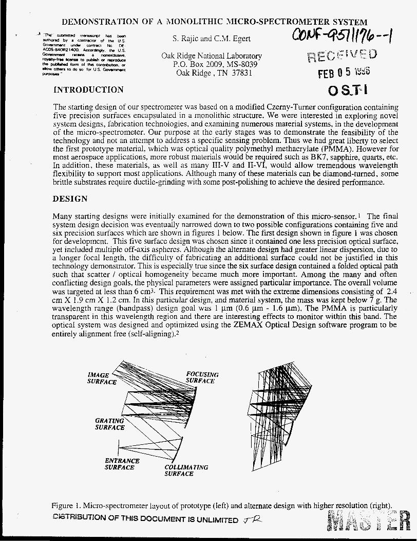
Many starting designs were initially examined for the demonstration of this micro-sensor. 1 The final system design decision was eventually narrowed down to two possible configurations containing five and six precision surfaces which are shown in figures 1 below. The first design shown in figure 1 was chosen for development. This five surface design was chosen since it contained one less precision optical surface, yet included multiple off-axis aspheres. Although the alternate design had greater linear dispersion, due to a longer focal length, the difficulty of fabricating an additional surface could not be justified in this technology demonstrator. This is especially true since the six surface design contained a folded optical path such that scatter / optical homogeneity became much more important. Among the many and often conflicting design goals, the physical parameters were assigned particular importance. The overall volume was targeted at less than 6 cm3. This requirement was met with the extreme dimensions consisting of 2.4 crn X 1.9 crn X 1.2 cm. In this particular design, and material system, the mass was kept below 7 g. The wavelength range (bandpass) design goal was 1 pm (0.6 pm - 1.6 pm). The PMMA is particularly transparent in this wavelength region and there are interesting effects to monitor within this band. The optical system was designed and optimized using the ZEMAX Optical Design software program to be entirely alignment free (self-aligning).2
ENTRANCE * SURFACE COLLIMA TING
SURFACE
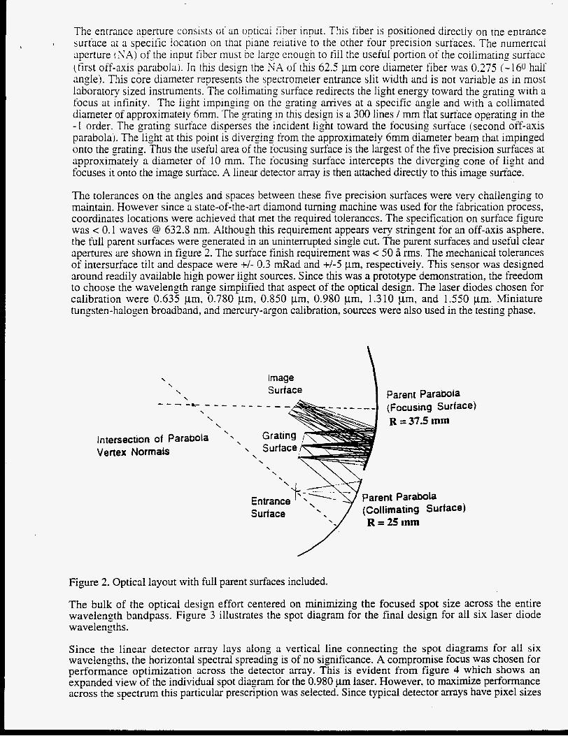
The entrance aperture consists OP an optical fiber input. This fiber is positioned directiv on the entrance surface at a specific location on that plane reiative to the other four precision surfaces. The numerical Liperture I XA) of the input fiber must be large enough to fill the useful portion of the collimating surrace (first off-axis parabola). In this design the NA of this 62.5 ,urn core diameter fiber was 0.275 (-160 haif anglej. This core diameter represents the spectrometer entrance slit width and is not variable as in most laboratory sized instruments. The collimating surface redirects the light energy toward the grating. with a focus at infinity. The light impinging on the grating arrives at a specific angle and with a collimated diameter of approximately 6mm. The grating in th s design is a 300 lines / mm tlat surface opgrating in the - 1 order. The grating surface disperses the incident light toward the focusing surface (second off-axis parabola,. The light at this point is diverging from the approximately 6mm diameter beam that impinged onto the grating. Thus the useful area of the focusing surface is the largest of the five precision surfaces at approximately a diameter of 10 mm. The focusing surface intercepts the diverging cone of light and focuses it onto the image surface. A linear detector array is then attached directly to this image suriace.
I
The tolerances on the angles and spaces between these five precision surfaces were very challenging to maintain. However since a state-of-the-art diamond turning machine was used for the fabrication process, coordinates locations were achieved that met the required tolerances. The specification on surface figure was e 0.1 waves 0 632.8 nm. Although this requirement appears very stringent for an off-axis asphere, the full parent surfaces were generated in an uninterrupted single cut. The parent surfaces and useful clear apertures are shown in figure 2. The surface finish requirement was < 50 S rms. The mechanical tolerances of intersurface tilt and despace were +/- 0.3 d a d and +/-5 pm, respectively. This sensor was designed around readily available high power light sources. Since this was a prototype demonstration, the freedom to choose the wavelength range simplified that aspect of the optical design. The laser diodes chosen for calibration were 0.635 pm, 0.780 pm, 0.850 pm, 0.980 pm, 1.310 pm, and 1.550 pm. Miniature tungsten-halogen broadband, and mercury-argon calibration, sources were also used in the testing phase.
\ \ image
\ Parent Paraoola \
-6- - - - - _ _ - - - - - - \
\ \
lntersecuon of Parabola '\
Vertex Normals
(Collimating Surface)
Figure 2. Optical layout with full parent surfaces included.
The bulk of the optical design effort centered on minimizing the focused spot size across the entire wavelength bandpass. Figure 3 illustrates the spot diagram for the final design for all six laser diode wavelengths.
Since the linear detector array lays along a vertical line connecting the spot diagrams for all six wavelengths, the horizontal spectral spreading is of no significance. A compromise focus was chosen for performance optimization across the detector array. This is evident from figure 4 which shows an expanded view of the individual spot diagram for the 0.980 pm laser. However, to maximize performance across the spectrum this particular prescription was selected. Since typical detector arrays have pixel sizes
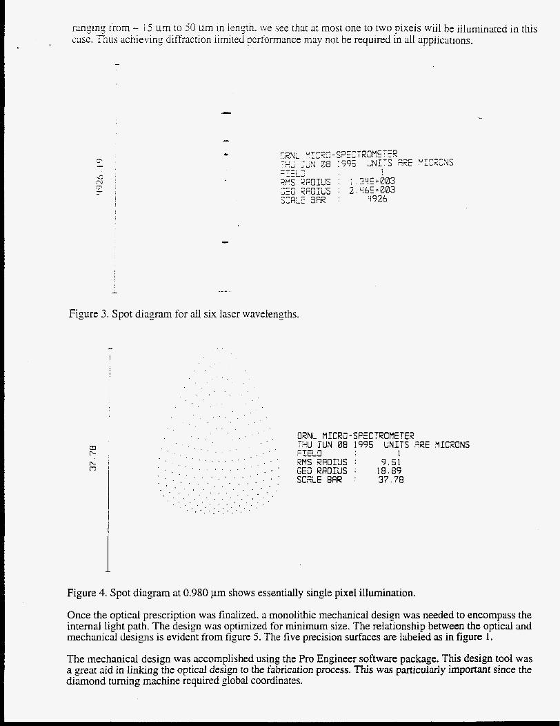
ranging rrom - i5 Ltrn to 5 0 urn in ienzrn. we see that at most one to two pixels will be illuminated in this case. Thus achieving diffraction iirnired performance may not be required in all appiications.
-
-
Figure 3. Spot diagram for all six laser wavelengths.
!
3 r- rc m . .
. . _ . . . . . . . . . . . . .
, . . _ . , _ . . . , . . . . . . . . . . . . . . . . ' . . . . . ' . . . .
ORNL MICRO TiiU TUN 08 FIELD RMS RADIUS GEO RROIUS SCALE ERR
-SPEC 1995
TROMETER W I T S ARE
I 9.51 18.89 37.78
MICRONS
Figure 4. Spot diagram at 0.980 pm shows essentially single pixel illumination.
Once the opticd prescription was finalized. a monolithic mechanical design was needed to encompass the internal light path. The design was optimized for minimum size. The relationship between the optical and mechanical designs is evident from figure 5. The five precision surfaces are labeled as in figure 1.
The mechanical design was accomplished using the Pro Engineer software package. This design tool was a great aid in linking the optical design to the fabrication process. This was particularly important since the diamond turning machine required global coordinates.
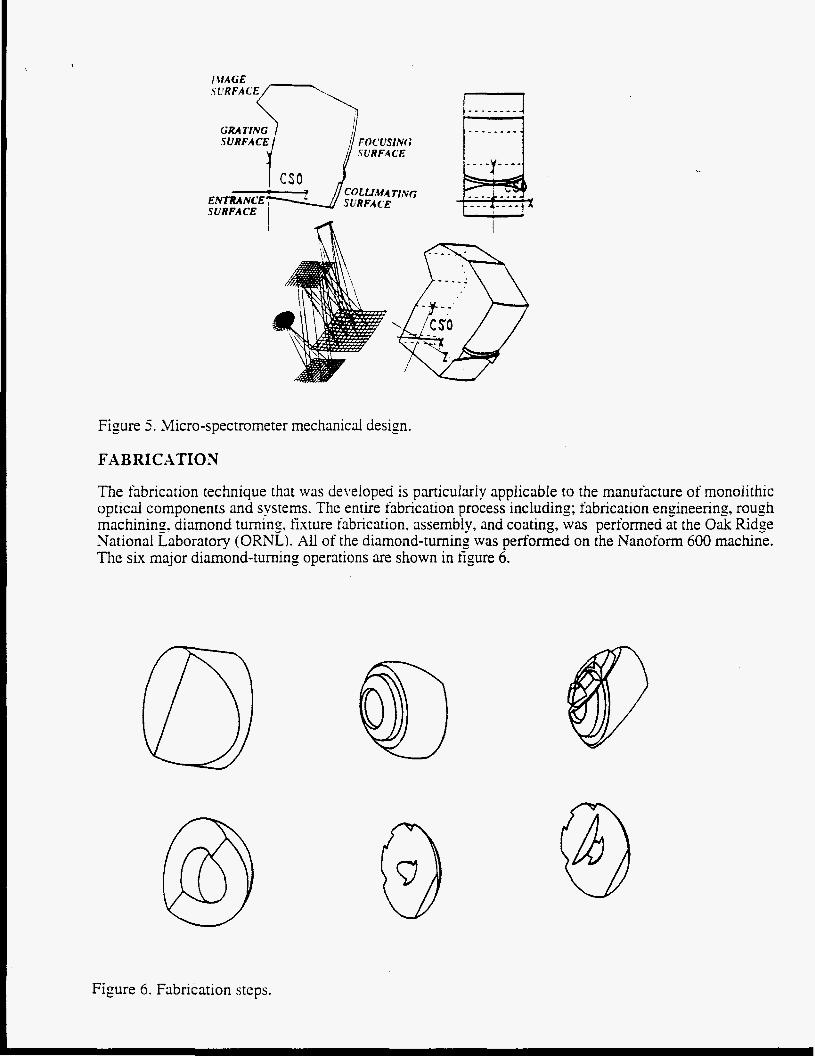
Figure 5. ,Micro-spectrometer mechanical design.
FABRICATION
The fabrication technique that was developed is particularly applicable to the manufacture of monolithic optical components and systems. The entire fabrication process including; fabrication engineering, rough machining, diamond turning, fixture fabrication, assembly, and coating, was performed at the Oak Ridge National Laboratory (ORNL). All of the diamond-turning was performed on the Nanoform 600 machine. The six major diamond-turning operations are shown in figure 6.
Figure 6. Fabrication steps.
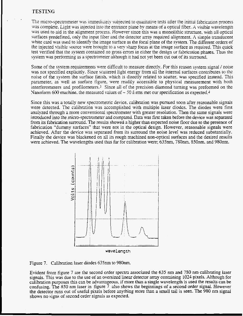
TESTING
The micro-spectrometer was immediatelv subjected to qualitative tests after the initial fabrication process was complete. Light was injected into rhe entrance piane by means of a optical fiber. A visible wavelength was used to aid in the alignment process. However since this was a monolithic structure, with all optical surfaces predefined, oniy the input fiber and the detector array required alignment. A simple translucent white card was used to identifi the image surface as the focal plane of the system. The different orders of the injected visible source were brought to a very sharp focus at the image surface as required. This quick test verified that the system contained no goss errors in either the design or fabrication phases. Thus the system was performing as a spectrometer although it had not yet been cut out of its surround.
Some of the system requirements were difficult to measure directly. For this reason svstem signal I’ noise was not specified explicitly. Since scattered light energy from all the internal surfaces contributes to the noise of the system the surface finish, which is directly related to scatter, was specified instead. This parameter, as’ well as surface figure, were readily accessible to physical measurement with both interferometers and profilometers.3 Since all of the precision diamond turning was preformed on the Nanoform 600 machine, the measured values of - 50 S rms met our specification as expected.4
Since this was a totally new spectrometric device. calibration was pursued soon after reasonable signals were detected. The calibration was accomplished with multiple laser diodes. The diodes were first analyzed through a more conventional spectrometer with greater resolution. Then the same signals were introduced into the micro-spectromerer and compared. Data was first taken before the device was separated from its fabrication surround. The results showed a higher than expected noise floor due to the presence of fabrication “dummy surfaces’’ that were not in the optical design. However, reasonable signals were achieved. After the device was separated from its surround the noise Ievei was reduced substantially. Finally the device was blackened on all its rough machined non-optical surfaces and the desired results were achieved. The wavelengths used thus far for calibration were: 635nm, 780nm. 850nm, and 980nm.
.... .
I . - , .... ... . .. .. ........ . .... r . . . . . . . . . . . . . . . . . . , . . . . .. . . . . . , . . . . . . . . . .. . . . . . . ... . . .. . . .
wavelength
Figure 7. Calibration laser diodes 635nm to 980nm.
Evident from figure 7 are the second order spectra associated the 635 nm and 750 nm calibrating laser signals. This was due to the use of an oversized linear detector array containing 1024 pixels. Although for calibration purposes this can be advantageous, if more than a single wavelength is used the results can be confusing. The 850 nm laser in figure 7 also shows the beginnings of a second order signal. However the detector runs out of useful pixels before anything more than a small tail is seen. The 980 nm signal shows no signs of second order signals as expected.
CONCLUSIONS
It now appears clear that ultra-precision monolithic sensors, such as a micro-spectrometer, can be successfully fabricated. The prototype system that has been demonstrated can now serve as the basis for low cost production techniques involving mold fabrication. This would include both the Sol-Gel technique, which can produce silica systems, as well as traditional plastic injection molding. The system was designed for a linear dispersion of -200 n d m m . However a design has been shown that, with the addition of a single flat surface, will produce a system with linear dispersion between 75-100 n d m m . This is typically sufficient for low / medium resolution sensor applications and would be tailored to the specific applications as required. The detailed analysis of the micro-spectrometer performance will be ongoing. The already identified applications include, emission mode laser warning receiver, transmission mode chemical / environmental detector, and a reflection mode corrosion monitor.
ACKNOWLEDGEMENTS
This work was sponsored by the laboratory directors research and development (LDRD) fund within the Oak Ridge National Laboratory (ORNL). O W L is managed by Lockheed Martin Energy Systems for the US. Department of Energy under contract no. DE-AC05-840R2 1400.
REFERENCES
1.
2 .
3.
4.
Instruments SA, JOBIN YVON/SPEX Division, Guide for Spectroscopy, Edison NJ, 1994.
S. Rajic, “Snap-Together Directed Energy Threat Protection System”, OSA, Optical Fabrication & Testing Workshop, 1992.
L.C. Maxey, “Novel Technique for Aligning Paraboloids”, SPIE VoI. 1532, Advanced Optical Manufacturing and Testing 11, 1991.
M.C. Gerchman, “Specifications and Manufacturing Considerations of Diamond-Turned Optical Components”,SPIE, O-E Lase, 1986.
DISCLAIMER
This report was prepared as an account of work sponsored by an agency of the United States Government. Neither the United States Government nor any agency thereof, nor any of their employees, makes any warranty, express or implied, or assumes any legal liability or responsi- bility for the accuracy, completeness, or usefulness of any information, apparatus, product, or process disclosed, or represents that its use would not infringe privately owned rights. Refer- ence herein to any specific commercial product, process, or service by trade name, trademark, manufacturer, or otherwise does not necessarily constitute or imply its endorsement, recom- mendation, or favoring by the United States Government or any agency thereof. The views and opinions of authors expressed herein do not necessarily state or reflect those of the United States Government or any agency thereof.
ENGINEERING TECHNOLOGY DIVISION APPROVAL FOR PREPARATION OF DOCUMENT
Classification: Unclassified
Date Needed:
1011 1 / 9 5
Titie: DEMONSTRATION OF A MONOLITHIC MICRO-SPECTROMETER SYSTEM
Reviewer: Roland D. Seals
I Author(s) (INDICATE IF FROM OTHER DIVISION OR ORGANIZATION): Raiic (16) . C. M. E ~ r t (15)
Section HeadlProgram Manager Approval:
GENERAL IN STR U CTlONS :
Please review the attached document by the date listed above for suitability and worth of the subject for presentation or publication, soundness of technlcal content, and clarity of presentation with respect to text, tables, graphs, and visual aids. You may note your comments on the attached draft, list them below, or note them on attached Sheets, whichever you prefer. Then please indicate your summary recommendation by checking the appropriate boxes below, sign this form, and return it with your comments to the author. Your assistance is greatly appreciated.
i recommend Its publication as submitted 0 i do not recommend publication of document mi recommend its publication i f revised as noted
It 0 needs, 0 does not need, editing (required for an ORNL report)
i &ave, 0 have not, reviewed this document with the author (not required)
Comments:
Technical Revie
ml have incorporated all comments n I have rejected some comments as noted Date
/ a - / a - 7r
ENGINEERING TECHNOLOGY DIVISION APPROVAL FOR PREPARATION OF DOCUMENT
Classification: Date Needed: Unclassified 10/ 11 /95
I
Reviewer: Kathv Hvlton
I Section Head/Program Manager Approval:
- Type of Document: ORNL Report NRC Report Journal Article Presentation [rl Other
I Presented at/Submitted to: International Conference on Integrated M i c r o - N a n o t e c W v v f o r
I Space Applications
i Title: DEMONSTRATION OF A MONOLITHIC MICRO-SPECTROMETER SYSTEM
Author(s) (INDICATE IF FROM OTHER DlVlSiON OR ORGANIZATION): S. Raiic (16) 9 C* M. (15)
G EN E R AL I N STR U CTI 0 N S :
Please review the attached document by the date listed above for suitability and worth of the subject for presentation or publication, soundness of technical content, and clarity of presentation with respect to text, tables, graphs, and visual aids. You may note your comments on the attached draft, list them below, or note them on attached sheets, whichever you prefer. Then please indicate your summary recommendation by checking the appropriate boxes below, sign this form, and return it with your comments to the author. Your assistance is greatly appreciated.
17 i recommend Its publication as submitted n , t ' d o not recommend publication of document
I recommend its publication if revised as noted
It [rlpeeds, 0 does not need, editing (required for an ORNL report)
I i have, have not, reviewed this document with the author (not required)
Comments:
Author:* Response to Reviewer's Comments: have incorporated all comments