defect-induced band-edge reconstruction of a...
TRANSCRIPT

Defect-Induced Band-Edge Reconstruction of a Bismuth-HalideDouble Perovskite for Visible-Light AbsorptionAdam H. Slavney,† Linn Leppert,§,# Davide Bartesaghi,‡,⊥ Aryeh Gold-Parker,†,∇ Michael F. Toney,∇
Tom J. Savenije,‡ Jeffrey B. Neaton,*,§,#,∥ and Hemamala I. Karunadasa*,†
†Department of Chemistry, Stanford University, Stanford, California 94305, United States§Molecular Foundry, Lawrence Berkeley National Laboratory, Berkeley, California 94720, United States#Department of Physics, University of California Berkeley, Berkeley, California 94720, United States‡Optoelectronic Materials Section, Department of Chemical Engineering, Delft University of Technology, 2628CD Delft, TheNetherlands⊥Materials Innovation Institute (M2i), 2628CD Delft, The Netherlands∇Stanford Synchrotron Radiation Lightsource, SLAC National Accelerator Laboratory, Menlo Park, California 94025, United States∥Kavli Energy NanoScience, Institute at Berkeley, Berkeley, California 94720, United States
*S Supporting Information
ABSTRACT: Halide double perovskites have recentlybeen developed as less toxic analogs of the lead perovskitesolar-cell absorbers APbX3 (A = monovalent cation; X =Br or I). However, all known halide double perovskiteshave large bandgaps that afford weak visible-lightabsorption. The first halide double perovskite evaluatedas an absorber, Cs2AgBiBr6 (1), has a bandgap of 1.95 eV.Here, we show that dilute alloying decreases 1’s bandgapby ca. 0.5 eV. Importantly, time-resolved photoconductiv-ity measurements reveal long-lived carriers with micro-second lifetimes in the alloyed material, which is verypromising for photovoltaic applications. The alloyedperovskite described herein is the first double perovskiteto show comparable bandgap energy and carrier lifetime tothose of (CH3NH3)PbI3. By describing how energy- andsymmetry-matched impurity orbitals, at low concentra-tions, dramatically alter 1’s band edges, we open apotential pathway for the large and diverse family ofhalide double perovskites to compete with APbX3absorbers.
Due to their rapid rise in power-conversion efficiencies, solarcells employing APbI3 perovskite absorbers are now being
considered for commercialization.1 However, the toxicity of thiswater-soluble Pb2+ source remains a critical concern for thematerials’ large-scale manufacture and use.2 The synthesis of aless toxic and stable analog that captures the remarkablephotophysical properties of APbI3 would constitute a criticaladvance in this field.3 To mimic the electronic properties ofAPbI3 we,
4 and others,5 recently replaced Pb2+ with nontoxic,isoelectronic Bi3+, by synthesizing the double perovskiteCs2AgBiBr6 (1) (Figure 1). Solid 1 is significantly more heatand moisture resistant than (MA)PbI3 (MA = CH3NH3
+).4
However, 1’s indirect bandgap of 1.95 eV4 provides inferior lightabsorption compared to the APbI3 perovskites, which have directgaps of ca. 1.6 eV. Here, we demonstrate how the photophysical
properties of 1 can be made competitive with those of (MA)PbI3through dilute alloying.The A2BB′X6 double perovskites offer far greater diversity of
B-site metals compared to ABX3 perovskites. Although there hasbeen much recent interest in halide double perovskites as solar-cell absorbers, these materials have so far displayed highbandgaps of 1.95−3.02 eV.4−6 Lead’s filled 6s orbitals at thevalence-band maximum (VBM) and empty 6p orbitals at theconduction-band minimum (CBM) play an important role inAPbI3’s strong direct-gap absorption (Figure 2a).7 The doubleperovskite (MA)2TlBiBr6 (2),6c where Pb2+ is replaced byisoelectronic Tl+ and Bi3+, has a similar orbital composition at itsband edges (Figure 2b). Although both (MA)PbI3 and 2 havedirect transitions, inclusion of Ag s (Ag d) orbitals in 1 shifts theCBM (VBM) leading to an indirect gap.5 We hypothesized thatincreasing 6s2 and 6p0 orbital character near 1’s band edges mayallow us to recover the direct gap of APbI3. We thereforeattempted to incorporate Tl+ as a dilute impurity into 1.Solid 1 crystallizes as translucent orange truncated octahedra.4
In contrast, adding TlBr to the crystallization solution affordsopaque black octahedral crystals of the Tl-alloyed perovskite: 1d(Figure 1). Using this method, the Tl content can be tunedacross the series Cs2(Ag1−aBi1−b)TlxBr6 (1d, 0.003 < x = a + b <
Received: February 15, 2017Published: March 29, 2017
Figure 1. Photographs of Cs2AgBiBr6 (1) and Cs2(Ag1−aBi1−b)TlxBr6(1d; x = a + b = 0.075) single crystals. Photograph of 1 reproduced fromref 4.
Communication
pubs.acs.org/JACS
© 2017 American Chemical Society 5015 DOI: 10.1021/jacs.7b01629J. Am. Chem. Soc. 2017, 139, 5015−5018
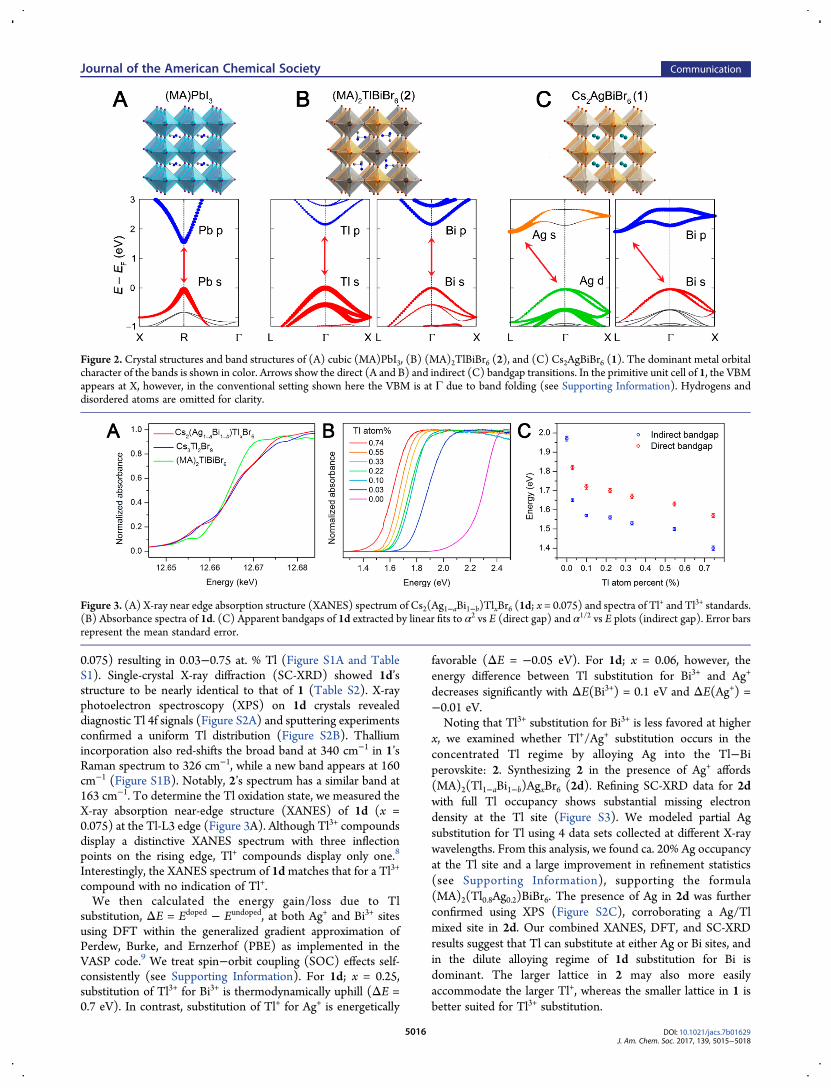
0.075) resulting in 0.03−0.75 at. % Tl (Figure S1A and TableS1). Single-crystal X-ray diffraction (SC-XRD) showed 1d’sstructure to be nearly identical to that of 1 (Table S2). X-rayphotoelectron spectroscopy (XPS) on 1d crystals revealeddiagnostic Tl 4f signals (Figure S2A) and sputtering experimentsconfirmed a uniform Tl distribution (Figure S2B). Thalliumincorporation also red-shifts the broad band at 340 cm−1 in 1’sRaman spectrum to 326 cm−1, while a new band appears at 160cm−1 (Figure S1B). Notably, 2’s spectrum has a similar band at163 cm−1. To determine the Tl oxidation state, we measured theX-ray absorption near-edge structure (XANES) of 1d (x =0.075) at the Tl-L3 edge (Figure 3A). Although Tl3+ compoundsdisplay a distinctive XANES spectrum with three inflectionpoints on the rising edge, Tl+ compounds display only one.8
Interestingly, the XANES spectrum of 1dmatches that for a Tl3+
compound with no indication of Tl+.We then calculated the energy gain/loss due to Tl
substitution, ΔE = Edoped − Eundoped, at both Ag+ and Bi3+ sitesusing DFT within the generalized gradient approximation ofPerdew, Burke, and Ernzerhof (PBE) as implemented in theVASP code.9 We treat spin−orbit coupling (SOC) effects self-consistently (see Supporting Information). For 1d; x = 0.25,substitution of Tl3+ for Bi3+ is thermodynamically uphill (ΔE =0.7 eV). In contrast, substitution of Tl+ for Ag+ is energetically
favorable (ΔE = −0.05 eV). For 1d; x = 0.06, however, theenergy difference between Tl substitution for Bi3+ and Ag+
decreases significantly with ΔE(Bi3+) = 0.1 eV and ΔE(Ag+) =−0.01 eV.Noting that Tl3+ substitution for Bi3+ is less favored at higher
x, we examined whether Tl+/Ag+ substitution occurs in theconcentrated Tl regime by alloying Ag into the Tl−Biperovskite: 2. Synthesizing 2 in the presence of Ag+ affords(MA)2(Tl1−aBi1−b)AgxBr6 (2d). Refining SC-XRD data for 2dwith full Tl occupancy shows substantial missing electrondensity at the Tl site (Figure S3). We modeled partial Agsubstitution for Tl using 4 data sets collected at different X-raywavelengths. From this analysis, we found ca. 20% Ag occupancyat the Tl site and a large improvement in refinement statistics(see Supporting Information), supporting the formula(MA)2(Tl0.8Ag0.2)BiBr6. The presence of Ag in 2d was furtherconfirmed using XPS (Figure S2C), corroborating a Ag/Tlmixed site in 2d. Our combined XANES, DFT, and SC-XRDresults suggest that Tl can substitute at either Ag or Bi sites, andin the dilute alloying regime of 1d substitution for Bi isdominant. The larger lattice in 2 may also more easilyaccommodate the larger Tl+, whereas the smaller lattice in 1 isbetter suited for Tl3+ substitution.
Figure 2. Crystal structures and band structures of (A) cubic (MA)PbI3, (B) (MA)2TlBiBr6 (2), and (C) Cs2AgBiBr6 (1). The dominant metal orbitalcharacter of the bands is shown in color. Arrows show the direct (A and B) and indirect (C) bandgap transitions. In the primitive unit cell of 1, the VBMappears at X, however, in the conventional setting shown here the VBM is at Γ due to band folding (see Supporting Information). Hydrogens anddisordered atoms are omitted for clarity.
Figure 3. (A) X-ray near edge absorption structure (XANES) spectrum of Cs2(Ag1−aBi1−b)TlxBr6 (1d; x = 0.075) and spectra of Tl+ and Tl3+ standards.
(B) Absorbance spectra of 1d. (C) Apparent bandgaps of 1d extracted by linear fits to α2 vs E (direct gap) and α1/2 vs E plots (indirect gap). Error barsrepresent the mean standard error.
Journal of the American Chemical Society Communication
DOI: 10.1021/jacs.7b01629J. Am. Chem. Soc. 2017, 139, 5015−5018
5016

To examine the optical effects of Tl alloying, reflectancespectra of 1 and 1d were converted to pseudoabsorbance spectrausing the Kubelka−Munk transformation10 and bandgaps wereextrapolated from αr vs photon energy (E) plots (r = 0.5 and 2for indirect and direct gaps, respectively; α = pseudoabsorptioncoefficient; Figures 3B,C, and S4). For 1, these data corroboratethe indirect bandgap previously reported.4,5 For 1d; x = 0.075,the data support either a direct gap of 1.6 eV or an indirect gap of1.4 eV (see Supporting Information). The bandgap energy dropssharply from 1.95 eV in 1 (indirect) to 1.72 eV (direct) or 1.57(indirect) in 1d; x = 0.010. At x > 0.010, the gap decreases moreslowly and reaches 1.40 eV (indirect) or 1.57 eV (direct) at thehighest alloying level of x = 0.075. Interestingly, the bandgapsthat arise from Tl alloying are much lower than those observedfor undoped 1 (1.95 eV) or for the fully Tl-substituted 2 (2.16eV). Notably, dilute Tl alloying brings 1’s bandgap within theideal range for a single-junction photovoltaic absorber.Dopants can form recombination trap states that decrease
carrier lifetime. We therefore performed time-resolved micro-wave photoconductivity (TRMC) measurements,11 to directlyprobe free-carrier lifetime. Although carrier lifetime decreasesupon alloying, 1d exhibits long-lived carriers (with microsecondlifetime; Figure S5), suggesting that carriers can be efficientlyextracted in a solar cell. Similar TRMC measurements on(MA)PbI3 crystals revealed a carrier lifetime of ca. 15 μs.12 Adetailed analysis of our TRMC measurements will be reportedseparately. Our results show that 1d is competitive with(MA)PbI3 with respect to two key indicators for an efficientabsorber: bandgap energy and carrier lifetime.We performed DFT calculations to determine the evolution of
1d’s electronic structure with Tl alloying, considering both Ag+
and Bi3+ substitution. Figure 2c shows 1’s band structurecalculated with DFT-PBE+SOC (see Supporting Information)with the conduction bands rigidly shifted to reproduce theexperimental bandgap. The CBM of 1 has Bi p character at Γ andBi p−Ag s character at L because completely symmetric Ag s−Bip hybridization is forbidden at Γ, but allowed at L. Thecalculated indirect (direct) bandgap is 1.09 eV (1.30 eV)underestimating experiment by ∼0.9 eV, as expected from DFT-PBE and similar to the trends reported for (MA)PbI3.
13 Toobtain quantitative optical gaps, a more advanced treatment ofexchange and correlation effects, including electron−holeinteractions, is required. However, we expect that computedtrends in bandgaps and relative energy differences betweendirect and indirect gaps will be captured reliably by DFT-PBE+SOC, at significantly less computational expense for thesecomplex systems. We then constructed 1d unit cells with 80,160, and 320 atoms, where in each case substitution of one B-siteatom with Tl corresponds to x = 0.13, x = 0.06, and x = 0.03,respectively. Keeping the lattice parameters fixed to those fromexperiment, we optimize all internal coordinates withoutsymmetry constraints using DFT-PBE, and subsequentlycalculate the band structure along high-symmetry directionsincluding spin−orbit interactions self-consistently. At x = 0.06,Tl+ substitution for Ag+ results in a direct gap at Γ and a bandgapreduction of ca. 0.1 eV (Figure 4A). Substitution of Tl3+ for Bi3+
shows a significantly larger bandgap reduction of ca. 0.8 eV,although the transition remains indirect (Figure 4B). Carriereffective masses for 1d; x = 0.06 and for 1 are shown in Table S6;higher alloying levels may further increase band dispersion.Calculations for other x values are shown in Figures S6 and S7.We also constructed a 1d unit cell with 320 atoms in which wesubstituted Tl+ and Tl3+ at both Ag+ and Bi3+ sites (1d; a = 0.03
and b = 0.03). This leads to a bandgap reduction of ca. 0.6 eV andan indirect bandgap only ca. 0.1 eV smaller than the directtransition at Γ(Figure S8). Calculations for only Tl3+
substitution and for mixed Tl+/Tl3+ substitution both agreewell with our optical data.Consolidating our experimental and theoretical results we
offer a model to explain the possible changes in 1’s electronicstructure upon dilute Tl alloying. Initial introduction of Tl+
produces defect levels derived from Tl 6s2 and 6p0 orbitals,whereas introduction of Tl3+ affords defect levels stemming fromTl 5d10 and 6s0 orbitals. At low doping levels, this results inlocalized perturbations in the periodic lattice potential extendingaround the Tl impurity. As the Tl concentration increases, theaverage distance between Tl impurities rapidly diminishes. Forexample, at 0.1 at. % Tl (∼1019 atoms/cm3) the average distancebetween Tl atoms is 3.3 nm or ca. 3 unit cells and the localizedimpurity states interact with each other and the host lattice tomodify the band edges. For Tl3+ substitution at Bi3+, the averageenergy of the empty Tl s states is below 1’s CBM, resulting in anew band that reduces the bandgap. This new band has Tl s andAg d character and is consequently similar to the highest VB of 1,placing the CBM at L. Comparable bandgap narrowing has beenobserved for isovalent alloying of GaAs1−xNx
14 andGaN1−xSbx.
15
Considering Tl+ substitution at Ag+, the average energy of thefilled Tl s states is above 1’s VBM, enabling a slight bandgapreduction. Additionally, Tl+ substitution for Ag+ introduces Tl pstates at Γ that hybridize with Br p and Bi p orbitals, lowering theenergy of the CBM at Γ and generating a direct gap. (FigureS6B). For equal substitution at both Ag and Bi sites, the CBM isdominated by the lower-energy Tl3+-derived s orbitals instead ofthe higher-energy Tl+-derived p orbitals, which maintains theindirect bandgap.
Figure 4. Band structures of Cs2(Ag1−aBi1−b)TlxBr6 (1d; x = 0.06) for(A) substitution of Tl+ for Ag+ and (B) substitution of Tl3+ for Bi3+.Metal orbital characters of the bands are shown in color.
Journal of the American Chemical Society Communication
DOI: 10.1021/jacs.7b01629J. Am. Chem. Soc. 2017, 139, 5015−5018
5017

Solid 1d retains the stability displayed by 1,4 with no changesin its PXRD patterns upon exposure to 0.75 sun at ca. 60 °Cunder N2 for 30 days, 90 °C in air for 5 days, and 55% relativehumidity under N2 for 30 days (Figure S9). Although Tl+ is ca.10 times more toxic than Pb2+, complete replacement of Pb2+
with a fraction of Tl+ results in an overall decrease in toxicity.Although semiconductor doping has played a central role in thephotovoltaics industry, the effects of doping APbX3 perovskitesare only just being explored. The most pronounced effects havebeen seen in heavily alloyed (MA)Pb1−xSnxI3, where x = 0.25−0.5 afforded a 0.4 eV bandgap reduction,16 and in doped(MA)Pb1−xBixBr3 where x = 0.03 resulted in a 0.3 eV bandgapdecrease.17
Here we demonstrate that halide double perovskites have richsubstitutional chemistry, which can engender dramatic changesto their photophysical properties. In the concentrated Tl regime,Tl+/Ag+ site mixing occurs readily, as in (MA)2(Tl1−aBi1−b)-AgxBr6 (2d; x = 0.2). At lower Tl levels, Tl3+ appears topredominantly substitute for Bi3+ as in Cs2(Ag1−aBi1−b)TlxBr6(1d; x = 0.075). Optical spectra reveal that the latter results in abandgap decrease of ca. 0.5 eV. Calculations show that dilute Tl+
alloying (x = 0.06) at Ag+ sites in 1d results in a 0.1 eV bandgapreduction and conversion to a direct gap, whereas Tl3+
substitution at Bi3+ sites affords a 0.8 eV reduction in bandgap,with the gap remaining indirect. Predominant substitution ofTl3+ for Bi3+ in 1d, where atmospheric oxygen mediates theoxidation of Tl+ to Tl3+, is most consistent with our experimentalresults.The optoelectronic properties of 1d motivate the continued
exploration of impurity alloying in double perovskites.Importantly, by describing how dopant orbitals at lowconcentrations selectively modify 1’s band edges, we provideguidelines for identifying other dopants that can afford largebandgap reductions and direct-gap transitions in environ-mentally benign double perovskites.
■ ASSOCIATED CONTENT*S Supporting InformationThe Supporting Information is available free of charge on theACS Publications website at DOI: 10.1021/jacs.7b01629.
Experimental details, crystallographic data, and spectra(PDF)Data for AgBiBr6Cs2 (CIF)Data for C2H12Ag0.2BiBr6N2Tl0.8 (CIF)Data for C2H12BiBr6N2Tl (CIF)
■ AUTHOR INFORMATIONCorresponding Authors*[email protected]*[email protected] F. Toney: 0000-0002-7513-1166Hemamala I. Karunadasa: 0000-0003-4949-8068NotesThe authors declare no competing financial interest.
■ ACKNOWLEDGMENTSWe thank Adam Jaffe, Dr. Yu Lin, Dr. Simon Teat, MatthewLatimer, Erik Nelson, and Jung-Hoon Lee for experimentalassistance. SC-XRD experiments used beamline 11.3.1 at theAdvanced Light Source (ALS). XANES measurements used
beamline 2-2 at the Stanford Synchrotron Radiation Lightsource(SSRL). A.H.S. is supported by a Stanford Graduate Fellowship.This work was funded by the SLAC National AcceleratorLaboratory and the Alfred P. Sloan Fellowship. J.B.N. and L.L.were supported by the U.S. Department of Energy, Office ofScience, Office of Basic Energy Sciences (DOE, BES), MaterialsSciences and Engineering Division (DE-AC02-05CH11231).L.L. is supported by the Feodor-Lynen program of the Alexandervon Humboldt foundation. Work at the Molecular Foundry,ALS, and SSRL was supported by the DOE, BES (DE-AC02-05CH11231 for the Molecular Foundry and ALS, and DE-AC02-76SF00515 for SSRL). Work by D.B. and T.J.S. wasfunded by the Partnership Program of the Materials InnovationInstitute M2i and the Foundation of Fundamental Research onMatter, Netherlands Organization for Scientific Research(F71.4.15562a). A.G.-P. is supported by an NSF GRFP (DGE-1147470).
■ REFERENCES(1) (a) Kojima, A.; Teshima, K.; Shirai, Y.; Miyasaka, T. J. Am. Chem.Soc. 2009, 131, 6050. (b) Zhang, W.; Eperon, G. E.; Snaith, H. J. Nat.Energy 2016, 1, 16048.(2) (a) Needleman, H. Annu. Rev. Med. 2004, 55, 209. (b) Babayigit,A.; Ethirajan, A.; Muller, M.; Conings, B. Nat. Mater. 2016, 15, 247.(3) Slavney, A. H.; Smaha, R. W.; Smith, I. C.; Jaffe, A.; Umeyama, D.;Karunadasa, H. I. Inorg. Chem. 2017, 56, 46.(4) Slavney, A. H.; Hu, T.; Lindenberg, A. M.; Karunadasa, H. I. J. Am.Chem. Soc. 2016, 138, 2138.(5) McClure, E. T.; Ball, M. R.; Windl, W.; Woodward, P. M. Chem.Mater. 2016, 28, 1348.(6) (a) Volonakis, G.; Filip, M. R.; Haghighirad, A. A.; Sakai, N.;Wenger, B.; Snaith, H. J.; Giustino, F. J. Phys. Chem. Lett. 2016, 7, 1254.(b) Wei, F.; Deng, Z.; Sun, S.; Xie, F.; Kieslich, G.; Evans, D. M.;Carpenter, M. A.; Bristowe, P. D.; Cheetham, A. K.Mater. Horiz. 2016,3, 328. (c) Deng, Z.; Wei, F.; Sun, S.; Kieslich, G.; Cheetham, A. K.;Bristowe, P. J. Mater. Chem. A 2016, 4, 12025. (d) Volonakis, G.;Haghighirad, A. A.; Milot, R. L.; Sio, W. H.; Filip, M. R.; Wenger, B.;Johnston, M. B.; Herz, L. M.; Snaith, H. J.; Giustino, F. J. Phys. Chem.Lett. 2017, 8, 772.(7) Filippetti, A.; Mattoni, A. Phys. Rev. B: Condens. Matter Mater. Phys.2014, 89, 125203.(8) Arvind, A.; Vishnoi, A. N. Phys. Scr. 2005, 2005, 534.(9) (a) Perdew, J. P.; Burke, K.; Ernzerhof, M. Phys. Rev. Lett. 1996, 77,3865. (b) Kresse, G.; Furthmuller, J. Phys. Rev. B: Condens. Matter Mater.Phys. 1996, 54, 11169.(10) Kubelka, P.; Munk, F. Z. Technol. Phys. 1931, 12, 593.(11) Savenije, T. J.; Ferguson, A. J.; Kopidakis, N.; Rumbles, G. J. Phys.Chem. C 2013, 117, 24085.(12) Bi, Y.; Hutter, E. M.; Fang, Y.; Dong, Q.; Huang, J.; Savenije, T. J.J. Phys. Chem. Lett. 2016, 7, 923.(13) Brivio, F.; Butler, K. T.; Walsh, A.; van Schilfgaarde, M. Phys. Rev.B: Condens. Matter Mater. Phys. 2014, 89, 155204.(14) Weyers, M.; Sato, M.; Ando, H. Jpn. J. Appl. Phys. 1992, 31, L853.(15) Sunkara, S.; Vendra, V. K.; Jasinski, J. B.; Deutsch, T.; Andriotis,A. N.; Rajan, K.; Menon, M.; Sunkara, M. Adv. Mater. 2014, 26, 2878.(16) Hao, F.; Stoumpos, C. C.; Chang, R. P. H.; Kanatzidis, M. G. J.Am. Chem. Soc. 2014, 136, 8094.(17) Abdelhady, A. L.; Saidaminov, M. I.; Murali, B.; Adinolfi, V.;Voznyy, O.; Katsiev, K.; Alarousu, E.; Comin, R.; Dursun, I.; Sinatra, L.;Sargent, E. H.; Mohammed, O. F.; Bakr, O. M. J. Phys. Chem. Lett. 2016,7, 295.
Journal of the American Chemical Society Communication
DOI: 10.1021/jacs.7b01629J. Am. Chem. Soc. 2017, 139, 5015−5018
5018