december 2008 joint industry standard · cv david corbett, defense supply center columbus robert...
TRANSCRIPT

JOINTINDUSTRY
STANDARD
Solderability Tests for
Component Leads,
Terminations, Lugs,
Terminals and Wires
EIA/IPC/JEDEC J-STD-002DJune 2013
Supersedes J-STD-002Cw/Amendment 1December 2008
®
SINGLE USER LICENSE - NOT FOR USE ON A NETWORK OR ONLINE

Notice ECIA, IPC and JEDEC Standards and Publications are designed to serve thepublic interest through eliminating misunderstandings between manufacturersand purchasers, facilitating interchangeability and improvement of products,and assisting the purchaser in selecting and obtaining with minimum delaythe proper product for his particular need. Existence of such Standards andPublications shall not in any respect preclude any member or nonmemberof ECIA, IPC or JEDEC from manufacturing or selling products not conformingto such Standards and Publications, nor shall the existence of such Standardsand Publications preclude their voluntary use by those other than ECIA, IPCor JEDEC members, whether the standard is to be used either domesticallyor internationally.
Recommended Standards and Publications are adopted by ECIA, IPC or JEDECwithout regard to whether their adoption may involve patents on articles, materials,or processes. By such action, ECIA, IPC or JEDEC do not assume any liability toany patent owner, nor do they assume any obligation whatever to parties adoptingthe Recommended Standard or Publication. Users are also wholly responsible forprotecting themselves against all claims of liabilities for patent infringement. Thematerial in this joint standard was developed by the IPC Components and WireSolderability Specification Task Group (5-23b) of the Assembly and JoiningProcesses Committee (5-20), the Electronic Components Industry AssociationSoldering Technology Committee (STC) and the JEDEC Solid State TechnologyAssociation Committee (JC14.1)
For Technical Information Contact:
EIA Standards
Electronic Components
Industry Association
2214 Rock Hill Rd, Suite 170Herndon, VA 20170-4212Phone: (571) 323-0294Fax: (571) 323-0245
IPC
Association Connecting
Electronics Industries®3000 Lakeside Drive, Suite 309SBannockburn, IL 60015-1249Phone: (847) 615-7100Fax: (847) 615-7105
JEDEC Solid State Technology
Association
3103 North 10th Street, Suite 240-SArlington, VA 22201-2107Phone: (703) 907-7540Fax: (703) 907-7583
Please use the Standard Improvement Form shown at the end of thisdocument.
©Copyright 2013. EIA, Herndon, Virginia, IPC, Bannockburn, Illinois, and JEDEC, Arlington, Virginia, USA. All rights reserved under bothinternational and Pan-American copyright conventions. Any copying, scanning or other reproduction of these materials without the priorwritten consent of the copyright holder is strictly prohibited and constitutes infringement under the Copyright Law of the United States.
SINGLE USER LICENSE - NOT FOR USE ON A NETWORK OR ONLINE

EIA/IPC/JEDEC J-STD-002D
Solderability Tests
for Component Leads,
Terminations, Lugs,
Terminals and Wires
A joint standard developed by IPC Components and Wire SolderabilitySpecification Task Group (5-23b) of the Assembly and Joining ProcessesCommittee (5-20), the Electronic Components Industry AssociationSoldering Technology Committee (STC) and the JEDEC Solid StateTechnology Association Committee (JC14.1)
Users of this standard are encouraged to participate in thedevelopment of future revisions.
Contact:
EIA Standards
Electronic Components
Industry Association
2214 Rock Hill Road, Suite 170Herndon, VA 20170-4212Phone: (571) 323-0294Fax: (571) 323-0245
IPC
Association Connecting
Electronics Industries®3000 Lakeside Drive, Suite 309SBannockburn, IL 60015-1249Phone: (847) 615-7100Fax: (847) 615-7105
JEDEC Solid State Technology
Association
3103 North 10th Street, Suite 240-SArlington, VA 22201-2107Phone: (703) 907-7540Fax: (703) 907-7583
Supersedes:J-STD-002C w/Amendment 1 -
November 2008J-STD-002C - December 2007Amendment 1 - October 2008J-STD-002B - February 2003J-STD-002A - October 1998J-STD-002 - April 1992
®
SINGLE USER LICENSE - NOT FOR USE ON A NETWORK OR ONLINE

This Page Intentionally Left Blank
SINGLE USER LICENSE - NOT FOR USE ON A NETWORK OR ONLINE

AcknowledgmentAny document involving a complex technology draws material from a vast number of sources. While the principal membersof the IPC Components and Wire Solderability Specification Task Group (5-23b) of the Assembly and Joining ProcessesCommittee (5-20) are shown below, it is not possible to include all of those we assisted in the evolution of this joint indus-try standard. Additionally, there were many participants from the Electronic Components Industry Association SolderingTechnology Committee (STC) and the JEDEC JC-14.1 Reliability Test Methods for Packaged Devices. To each of them, themembers and staffs of IPC, ECIA and JEDEC Associations extend their gratitude.
IPC Assembly & JoiningProcesses Committee
IPC Component & Wire SolderabilitySpecification Task Group
EIA SolderingTechnology Committee
ChairLeo P. LambertEPTAC Corporation
Vice ChairRenee J. MichalkiewiczTrace Laboratories - Baltimore
ChairDavid D. HillmanRockwell Collins
Vice ChairDennis FritzMacDermid, Inc.
ChairDouglas W. RommTexas Instruments Inc.
JEDEC JC14.1 Reliability TestMethods for Packaged Devices
ChairIfe HsuIntel Corporation
IPC Component & Wire Solderability Specification Task Group
Ross Dillman, ACI/EMPF
Constantino Gonzalez, ACMETraining & Consulting
Neil Witkowski, Alcatel-Lucent
Bradley Smith, Allegro MicroSystemsInc.
Karen Tellefsen, Alpha
Andrew Giamis, Andrew Corporation
George Wenger, Andrew Corporation
Greg Alexander, Ascentech, LLC
Fritz Byle, Astronautics Corp. ofAmerica
Jeffery Kukelhan, BAE SystemsPlatform Solutions
Marvin Banks, Ball Aerospace &Technologies
Gerald Leslie Bogert, Bechtel PlantMachinery, Inc.
Robert Wettermann, BEST Inc.
Beverley Christian, BlackBerry
Thomas Carroll, Boeing Company
Michael Paddack, Boeing Company
Mary Bellon, Boeing Research &Development
Michael Jawitz, Boeing Research &Development
Todd MacFadden, Bose Corporation
Jason Bragg, Celestica
Prakash Kapadia, Celestica
Louis Hart, Compunetics Inc.
Mark Fulcher, ContinentalAutomotive Systems
Brian Madsen, ContinentalAutomotive Systems
Jose Servin, Continental Temic SA deCV
David Corbett, Defense SupplyCenter Columbus
Robert Heber, Defense Supply CenterColumbus
Lowell Sherman, Defense SupplyCenter Columbus
Glenn Dody, Dody Consulting
Michael Toben, Dow ElectronicMaterials
Anne Lomonte, Draeger MedicalSystems, Inc.
Peter Bratin, ECI Technology, Inc.
Michael Pavlov, ECI Technology, Inc.
Karl Wengenroth, Enthone Inc.
Yung-Herng Yau, Enthone Inc.
Leo Lambert, EPTAC Corporation
Thomas Carlstrom, Ericsson AB
Gerald Gagnon, Extech InstrumentsCorporation
John Thompson, FCI USA, Inc.
Harjinder Ladhar, Flextronics
Terry Munson, Foresite, Inc.
Paco Solis, Foresite, Inc.
Martin Bayes, Four SquareConsulting
Michael Yuen, FoxconnCMMSG-NVPD
Graham Naisbitt, Gen3 SystemsLimited
Brian Wardhaugh, Gen3 SystemsLimited
Gregg Klawson, General Dynamics -C4 Systems
Donald Gerstle, Google
Brian Toleno, Henkel Corporation
Richard Davidson, HoneywellAerospace
June 2013 EIA/IPC/JEDEC J-STD-002D
iii
SINGLE USER LICENSE - NOT FOR USE ON A NETWORK OR ONLINE

Suzanne Nachbor, HoneywellAerospace Minneapolis
Vicka White, Honeywell Inc. AirTransport Systems
Fujiang Sun, Huawei TechnologiesCo., Ltd.
Yunhua (Danny) Tu, HuaweiTechnologies Co., Ltd.
James Bielick, IBM Corporation
James Maguire, Intel Corporation
Mark Kwoka, Intersil Corporation
Reza Ghaffarian, Jet PropulsionLaboratory
J. Lee Parker, JLP
David Scheiner, Kester
David Lober, Kyzen Corporation
Todd Jarman, L-3 Communications
Roger Su, L-3 Communications
Vijay Kumar, Lockheed MartinMissile & Fire Control
Linda Woody, Lockheed MartinMissile & Fire Control
Hue Green, Lockheed Martin SpaceSystems Company
Dennis Fritz, MacDermid, Inc.
Francis Anglade, Metronelec
Laya (Yan) Chen, Microtek(Changzhou) Laboratories
Russell Shepherd, MicrotekLaboratories Anaheim
Edwin Bradley, Motorola Solutions,Inc.
Christopher Hunt, National PhysicalLaboratory
Keith Sweatman, Nihon Superior Co.,Ltd.
Kil-Won Moon, NIST
Maureen Williams, NIST
Darrell Freiwald, Northrop Grumman
Mahendra Gandhi, NorthropGrumman Aerospace Systems
Joseph Sherfick, NSWC Crane
Richard Kraszewski, Plexus Corp.
Carol Handwerker, Purdue University
Bill Beair, Raytheon Company
Richard Iodice, Raytheon Company
Jeff Seekatz, Raytheon Company
Jeff Shubrooks, Raytheon Company
Royce Taylor, Raytheon Company
Bill Vuono, Raytheon Company
Lance Brack, Raytheon MissileSystems
Robert Morris, Raytheon MissileSystems
Martin Scionti, Raytheon MissileSystems
William Russell, RaytheonProfessional Services LLC
Steven Herrberg, Raytheon SystemsCompany
Christian Klein, Robert Bosch GmbH
Jason Koch, Robisan Laboratory Inc.
Chris Mahanna, Robisan LaboratoryInc.
David Adams, Rockwell Collins
DeAnn Gibbs, Rockwell Collins
Rachel Grinvalds, Rockwell Collins
David Hillman, Rockwell Collins
Eddie Hofer, Rockwell Collins
Gaston Hidalgo, SamsungTelecommunications America
Henry Rekers, Schneider Electric
Giovanni Casanova, SchweitzerEngineering Laboratories, Inc.
Donald Abbott, Sensata Technologies
Gerard O’Brien, Solderability Testing& Solutions, Inc.
Stephen Meeks, St. Jude Medical
Mel Parrish, STI Electronics, Inc.
Christine Blair, STMicroelectronicsInc.
William Sepp, Technic Inc.
Richard Edgar, Tec-Line Inc.
Douglas Romm, Texas InstrumentsInc.
Shirley He, The 5th ElectronicInstitute of MII
Elizabeth Allison, Trace Laboratories- Baltimore
Renee Michalkiewicz, TraceLaboratories - Baltimore
Debora Obitz, Trace Laboratories -Baltimore
John Radman, Trace Laboratories -Denver
Calette Chamness, U.S. ArmyAviation & Missile Command
Jere Wittig, Unknown Address
George Milad, Uyemura InternationalCorp.
Chris Ball, Valeo Inc.
Dale Albright, Winslow Automationaka Six Sigma
Russell Winslow, WinslowAutomation aka Six Sigma
Theodore Edwards
John Rohlfing
EIA/IPC/JEDEC J-STD-002D June 2013
iv
SINGLE USER LICENSE - NOT FOR USE ON A NETWORK OR ONLINE

Table of Contents
1 PREFACE .................................................................. 1
1.1 Scope ..................................................................... 1
1.2 Purpose .................................................................. 1
1.2.1 Shall and Should ................................................... 1
1.3 Method Classification ........................................... 1
1.3.1 Visual Acceptance Criteria Tests .......................... 1
1.3.2 Force Measurement Tests ..................................... 1
1.4 Coating Durability ................................................ 2
1.5 Solderability Backwards Compatibility ................ 2
1.6 Referee Verification Solder Dip for Tests A,B, C, A1, B1, and C1 ........................................... 2
1.7 Limitations ............................................................ 2
1.8 Contractual Agreement ......................................... 2
1.9 Terms and Definitions ........................................... 2
2 APPLICABLE DOCUMENTS .................................... 3
2.1 Industry .................................................................. 3
2.1.1 IPC ......................................................................... 3
2.1.2 International Electrotechnical Commission .......... 3
2.2 Government ........................................................... 3
2.2.1 Federal ................................................................... 3
3 REQUIREMENTS ...................................................... 3
3.1 Materials ................................................................ 3
3.1.1 Solder .................................................................... 3
3.1.2 Flux ........................................................................ 3
3.1.3 Standard Copper Wrapping Wires ........................ 4
3.1.4 Water ..................................................................... 4
3.2 Equipment ............................................................. 4
3.2.1 Steam Preconditioning Apparatus ........................ 4
3.2.2 Bake Preconditioning Apparatus .......................... 4
3.2.3 Optical Inspection Equipment .............................. 5
3.2.4 Dipping Equipment ............................................... 5
3.2.5 Timing Equipment ................................................ 5
3.3 Preparation for Testing ......................................... 5
3.3.1 Specimen Preparation and Surface Condition ..... 5
3.3.2 Steam Conditioning .............................................. 6
3.3.3 Surfaces to be Tested ............................................ 6
3.4 Solder Bath Requirements .................................... 6
3.4.1 Solder Contamination Control .............................. 6
4 TEST PROCEDURES ............................................... 7
4.1 Application of Flux ............................................... 7
4.2 Visual Acceptance Criteria Tests .......................... 7
4.2.1 Test A - SnPb Solder – Solder Bath/Dipand Look Test (Leads, Wires, etc.) ...................... 7
4.2.2 Test B - SnPb Solder – Solder Bath/Dipand Look Test (Leadless Components) ................ 9
4.2.3 Test C - SnPb Solder – Wrapped WiresTest (Lugs, Tabs, Terminals, Large StrandedWires) .................................................................. 10
4.2.4 Test D - SnPb or Pb-free Solder –Resistance to Dissolution ofMetallization Test ................................................ 12
4.2.5 Test S - SnPb Solder – SurfaceMount Process Simulation Test .......................... 13
4.2.6 Test A1 - Pb-free Solder – Solder Bath/Dipand Look Test (Leads, Wires, etc.) .................... 14
4.2.7 Test B1 - Pb-free Solder – Solder Bath/Dipand Look Test (Leadless Components) .............. 15
4.2.8 Test C1 - Pb-free Solder – Wrapped WiresTest (Lugs, Tabs, Terminals, Large StrandedWires) .................................................................. 16
4.2.9 Test S1 - Pb-free Solder – Surface MountProcess Simulation Test ...................................... 17
4.3 Force Measurement Tests ................................... 19
4.3.1 Test E - SnPb Solder – Wetting BalanceSolder Pot Test (Leaded Components) ............... 19
4.3.2 Test F - SnPb Solder – Wetting Balance ........... 20
4.3.3 Test G - SnPb Solder – Wetting BalanceGlobule Test ........................................................ 22
4.3.4 Test E1 - Pb-free Solder – Wetting BalanceSolder Pot Test (Leaded Components) ............... 24
4.3.5 Test F1 - Pb-free Solder – Wetting BalanceSolder Pot Test (Leadless Components) ............ 25
4.3.6 Test G1 - Pb-free Solder – Wetting BalanceGlobule Test ........................................................ 26
5 NOTES ..................................................................... 27
5.1 Use of Activated Flux ......................................... 27
5.2 Massive Components .......................................... 27
5.3 Sampling Plans .................................................... 27
5.4 Correction for Buoyancy .................................... 27
5.5 Preconditioning Limitations ................................ 28
APPENDIX A Critical Component Surfaces ........... 29
APPENDIX B Evaluation Aids .................................. 38
APPENDIX C Calculation of MaximumTheoretical Force ............................... 43
APPENDIX D Calculation of Integrated Value ofArea of the Wetting Curve ................ 45
June 2013 EIA/IPC/JEDEC J-STD-002D
v
SINGLE USER LICENSE - NOT FOR USE ON A NETWORK OR ONLINE

APPENDIX E Informative Annex .............................. 46
APPENDIX F J-STD-002/J-STD-003 ActivatedSolderability Test Flux RationaleCommittee Letter ............................... 47
APPENDIX G Graphical Representations:Progression of Solder WettingCurve Parameters As MeasuredBy Wetting Balance Testing ............. 49
APPENDIX H Test Protocol for WettingBalance Gauge RepeatabilityandReproducibility (GR&R)Using Copper Foil Coupons ............. 52
Figures
Figure 3-1 Example Reticle ................................................ 5
Figure 4-1 Dipping Schematic ............................................ 8
Figure 4-2 Solder Dipping Angle for Surface MountLeaded Components ........................................ 8
Figure 4-3 Solder Dipping Depth for Through-HoleComponents ..................................................... 9
Figure 4-4 Leadless Component Immersion Depth ......... 10
Figure 4-5 Illustration of Acceptable SolderableTerminal .......................................................... 11
Figure 4-6 Illustration of Unsolderable Terminal .............. 11
Figure 4-7 Illustration of Acceptable SolderableStranded Wire ................................................. 11
Figure 4-8 Illustration of Partially Solderable StrandedWire Showing Incomplete Fillet ...................... 11
Figure 4-9 Wetting Balance Apparatus ............................ 19
Figure 4-10 Set A Wetting Curve ....................................... 21
Figure 4-11 Set B Wetting Curve ....................................... 21
Figure 4-12 Component and Dipping Angle (Directlyfrom IEC 60068-2-69) ..................................... 24
Figure A-1 ‘‘J’’ Leaded Components ................................ 29
Figure A-2 Passive Components ...................................... 30
Figure A-3 Gull Wing Components .................................. 31
Figure A-4 Leadless Chip Carrier ..................................... 32
Figure A-5 ‘‘L’’ Leaded Component .................................. 33
Figure A-6 Exposed Pad Package ................................... 34
Figure A-7 Bottom-Only Termination Component ............ 34
Figure A-8 Area Array Component Critical Surface ......... 35
Figure A-9 Through-Hole Components - Flat Pin ............ 36
Figure A-10 Through-Hole Components - Round Pin ........ 37
Figure B-1 Defect Size Aid ............................................... 38
Figure B-2 Types of Solderability Defects ........................ 39
Figure B-3 Aids in Evaluation of 5% AllowableArea of Pin Holes ........................................... 40
Figure B-4 Aid in Evaluation of 5% AllowableArea of Pin Holes ........................................... 41
Figure B-5 Solderability Coverage Guide ......................... 42
Figure C-1 Lead Periphery and Volume for a132 I/O PQFP ................................................. 43
Tables
Table 3-1 Flux Compositions ............................................... 4
Table 3-2 Steam Temperature Requirements ..................... 5
Table 3-3 Preconditioning Parameters for SolderabilityTesting ................................................................. 6
Table 3-4 Maximum Limits of Solder Bath Contaminant .... 7
Table 4-1 Test A Solderability Testing Parameters ............. 8
Table 4-2 Test B Solderability Testing Parameters ........... 10
Table 4-3 Test C Solderability Testing Parameters ........... 11
Table 4-4 Test D Solderability Testing Parameters ........... 13
Table 4-5 Stencil Thickness Requirements ....................... 13
Table 4-6 Reflow Parameter Requirements ...................... 14
Table 4-7 Test S Solderability Testing Parameters ........... 14
Table 4-8 Test A1 Solderability Testing Parameters ......... 15
Table 4-9 Test B1 Solderability Testing Parameters ......... 16
Table 4-10 Test C1 Solderability Testing Parameters ......... 17
Table 4-11 Stencil Thickness Requirements ....................... 18
Table 4-12 Pb-free Reflow Parameter Requirements ......... 18
Table 4-13 Test S1 Solderability Testing Parameters ......... 18
Table 4-14 Wetting Balance Parameter and SuggestedEvaluation Criteria ............................................. 20
Table 4-15 Dipping Angle and Immersion Depth forComponents (Directly from IEC 60068-2-69) ... 23
Table 4-16 Wetting Parameters and SuggestedEvaluation Criteria ............................................. 24
Table 3-1 Flux Compositions ............................................. 47
EIA/IPC/JEDEC J-STD-002D June 2013
vi
SINGLE USER LICENSE - NOT FOR USE ON A NETWORK OR ONLINE

Solderability Tests for Component Leads,Terminations, Lugs, Terminals and Wires
1 PREFACE
1.1 Scope This standard prescribes test methods, defect definitions, acceptance criteria, and illustrations for assessing thesolderability of electronic component leads, terminations, solid wires, stranded wires, lugs, and tabs. This standard alsoincludes a test method for the resistance to dissolution/dewetting of metallization. This standard is intended for use by bothvendor and user.
1.2 Purpose Solderability evaluations are made to verify that the solderability of component leads and terminations meetsthe requirements established in this standard and to determine that storage has had no adverse effect on the ability to soldercomponents to an interconnecting substrate. Determination of solderability can be made at the time of manufacture, at receiptof the components by the user, or just before assembly and soldering.
The resistance to dissolution of metallization determination is made to verify that metallized terminations will remain intactthroughout the assembly soldering processes.
In the case of a discrepancy, the description or written criteria always takes precedence over the illustrations.
1.2.1 Shall and Should The words ‘‘shall’’ or ‘‘shall not’’ are used in the text of this document wherever there is arequirement for materials, preparation, process control, or acceptance of a soldered connection or a test method. The word‘‘should’’ reflects recommendations and is used to reflect general industry practices and procedures for guidance only.
Other documents to extent specified by the customer.
1.3 Method Classification This standard describes methods by which component leads or terminations may be evaluatedfor solderability. Any one of the following test methods - Test A, Test B, Test C, Test D, and Test S - may be used for SnPbsolder processes and any one of the following test methods - Test A1, Test B1, Test C1, Test D, and Test S1 - may be usedfor Pb-free solder processes and are to be used for each application as a default unless otherwise AABUS.
1.3.1 Visual Acceptance Criteria Tests
Test A – Solder Bath/Dip and Look Test (Leaded Components and Stranded Wires) SnPb Solder (4.2.1)
Test B – Solder Bath/Dip and Look Test (Leadless Components) SnPb Solder (4.2.2)
Test C – Wrapped Wires Test (Lugs, Tabs, Hooked Leads, and Turrets) SnPb Solder (4.2.3)
Test D – Resistance to Dissolution/Dewetting of Metallization Test SnPb Solder and Pb-free Solder (4.2.4)
Test S – Surface Mount Process Simulation Test SnPb Solder (4.2.5)
Test A1 – Solder Bath/Dip and Look Test (Leaded Components and Stranded Wires) Pb-free Solder (4.2.6)
Test B1 – Solder Bath/Dip and Look Test (Leadless Components) Pb-free Solder (4.2.7)
Test C1 – Wrapped Wires Test (Lugs, Tabs, Hooked Leads, and Turrets) Pb-free Solder (4.2.8)
Test S1 – Surface Mount Process Simulation Test Pb-free Solder (4.2.9)
1.3.2 Force Measurement Tests
Test E – Wetting Balance Solder Pot Test (Leaded Components) SnPb Solder (4.3.1)
Test F – Wetting Balance Solder Pot Test (Leadless Components) SnPb Solder (4.3.2)
Test G – Wetting Balance Globule Test SnPb Solder (4.3.3)
Test E1 – Wetting Balance Solder Pot Test (Leaded Components) Pb-free Solder (4.3.4)
Test F1 – Wetting Balance Solder Pot Test (Leadless Components) Pb-free Solder (4.3.5)
Test G1 – Wetting Balance Globule Test Pb-free Solder (4.3.6)
June 2013 EIA/IPC/JEDEC J-STD-002D
1
SINGLE USER LICENSE - NOT FOR USE ON A NETWORK OR ONLINE

These methods (1.3.2) are included for evaluation purposes only. Data collected should be submitted to the IPC WettingBalance Task Group for correlation and analysis. Tests E, F, G, E1, F1 and G1 shall not be used for acceptance/rejectionwithout user and vendor agreement.
1.4 Coating Durability The following are guidelines, not specification requirements, for determining the needed level ofpreconditioning category assurance (see Table 3-3). The coating durability guidelines describe two broad usage sectors andare not intended to encompass all possible product use scenarios. The user and vendor need to agree on the coating dura-bility requirements. Coating Durability Category 2 is the default condition for all component finishes.
Category 1 – Minimum Coating Durability Intended for surfaces that will be soldered within a short period of time (e.g.,up to six months) from the time of testing and are likely to experience a minimum of thermal exposures before soldering.No preconditioning category per Table 3-3.
Category 2 – Typical Coating Durability Intended for surfaces whose solderability may become degraded from storage oflonger than six months or from multiple thermal exposures. This is preconditioning Category E per Table 3-3.
1.5 Solderability Backwards Compatibility Typically Pb containing terminations are evaluated using SnPb solderabilitytest conditions and Pb-free terminations use Pb-free test conditions. If Pb-free terminations are to be used in a SnPb solderprocess (backward compatibility) then they should be evaluated at 215°C using test parameters consistent with standardSnPb solder conditions. The backward compatibility test does not apply to Pb-free BGA type packages.
1.6 Referee Verification Solder Dip for Tests A, B, C, A1, B1, and C1 When the dipped portion of the termination exhib-its anomalies such as surface roughness, dross, or anomalies that may have been induced by improper solder dipping, a ref-eree verification solder dip of the suspect anomaly may be necessary. Upon reinspection, if the suspect anomaly has beenremoved, the anomaly will have been verified as a non-rejectable cosmetic surface defect. If the anomaly persists, regard-less of area it shall be classified a rejectable solderability defect. This procedure may only be used on one component perlot. Continuous need of Referee Verification Solder Dip procedure is an indication of either improper testing procedure,examination interpretation, or of poor component quality.
1.7 Limitations This standard shall not be construed as a production procedure for the pre-tinning of leads and termina-tions. Solderability testing of components is considered a destructive test and the tested component should not be used forfunctional electrical evaluation. Components after such solderability testing shall only be used AABUS.
1.8 Contractual Agreement In cases where the stated test parameters are inappropriate or insufficient, alternative param-eters may be AABUS.
1.9 Terms and Definitions Terms repeated from IPC-T-50 are indicated by an asterisk (*).
AABUS Abbreviation for ‘‘as agreed by user and supplier.’’
Dewetting* A condition that results when molten solder coats a surface and then recedes to leave irregularly-shapedmounds of solder that are separated by areas that are covered with a thin film of solder and with the basis metal not exposed.
Dissolution of Component Metallization (Leaching) The loss or removal of metallization from an area on the basis orsubstrate material after immersion in molten solder.
Equilibrium Wetting The degree of wetting in which the forces of wetting are in balance with the forces of gravity.
Nonwetting, Solder* The inability of molten solder to form a metallic bond with the basis metal.
Pinhole* An imperfection in the form of a small hole that penetrates through a layer of material.
Solderability* The ability of a metal to be wetted by molten solder.
Solder Connection Pinhole* A small hole that penetrates from the surface of a solder connection to a void of indetermi-nate size within the solder connection.
Wetting, Solder* The formation of a relatively uniform, smooth, unbroken, and adherent film of solder to a base metal.
EIA/IPC/JEDEC J-STD-002D June 2013
2
SINGLE USER LICENSE - NOT FOR USE ON A NETWORK OR ONLINE

2 APPLICABLE DOCUMENTS
The following documents of the issue currently in effect form a part of this standard to the extent specified herein.
2.1 Industry
2.1.1 IPC1
IPC-T-50 Terms and Definitions
J-STD-004 Requirements for Soldering Fluxes
J-STD-005 Requirements for Soldering Pastes
J-STD-006 Requirements for Electronic Grade Solder Alloys and Fluxed and Non-Fluxed Solid Solder for Electronic Sol-dering Applications
IPC-TR-464 Accelerated Aging for Solderability Evaluations and Addendum
IPC-TM-650 Test Methods Manual2
2.1.2 International Electrotechnical Commission3
IEC 60068-2-69 Environmental testing - Part 2-69: Tests - Test Te: Solderability testing of electronic components for sur-face mounting devices (SMD) by the wetting balance method
2.2 Government4
2.2.1 Federal5
(CID) A-A-59551 Wires, Electrical, Copper (Uninsulated)
3 REQUIREMENTS
3.1 Materials All chemicals shall be of commercial grade or better. Fresh solvents shall be used as often as is necessaryto preclude contamination.
3.1.1 Solder For SnPb testing, the solder composition shall be Sn60Pb40 or Sn63Pb37 per J-STD-006. The compositionof the solder, including contamination levels, shall be maintained during testing per 3.4.1.
For Pb-free testing, the solder composition shall be Sn96.5Ag3.0Cu0.5 (SAC305), allowing variation of the Ag contentbetween 3.0-4.0 wt% and Cu content between 0.5-1.0 wt% with the balance being Sn per J-STD-006. If no Pb-free solderalloy is specified, the default solder composition shall be Sn96.5Ag3.0Cu0.5 (SAC305) per J-STD-006. Other Pb-free sol-der alloys may be used AABUS.
The composition of the SnPb solder paste to be used in Test S shall be Sn60Pb40 or Sn63Pb37 for SnPb per J-STD-005,flux type ROL1. The solder paste shall meet the storage and shelf life requirements of the manufacturer’s specification.
The composition of the Pb-free solder paste to be used in Test S1 shall be Sn96.5Ag3.0Cu0.5 (SAC305), allowing varia-tion of the Ag content between 3.0 - 4.0 wt% and Cu content between 0.5 - 1.0 wt% with the balance being Sn per J-STD-005. If no Pb-free solder paste is specified, the default composition shall be Sn96.5Ag3.0Cu0.5 (SAC305) per J-STD-005,flux type to be AABUS. Other Pb-free paste solder alloys may be used AABUS. The solder paste shall meet the storage andshelf life requirements of the manufacturer’s specification.
3.1.2 Flux The flux for SnPb solderability tests shall be a standard activated rosin flux #1 having a composition of 25%± 0.5% by weight of colophony and 0.15% ± 0.01% by weight diethylammonium hydrochloride (CAS 660-68-4), in 74.85%± 0.5% by weight of isopropyl alcohol (see Table 3-1).
The flux for Pb-free solderability tests shall be standard activated rosin flux #2 having a composition of 25% ± 0.5% byweight of colophony and 0.39% ± 0.01% by weight diethylammonium hydrochloride (CAS 660-68-4), in 74.61% ± 0.5%by weight of isopropyl alcohol (see Table 3-1).
1. www.ipc.org2. Current and revised IPC Test Methods are available on the IPC Web site (www.ipc.org/html/testmethods.htm)3. www.iec.ch4. apps.fas.gsa.gov5. http://astimage.daps.dla.mil/quicksearch/
June 2013 EIA/IPC/JEDEC J-STD-002D
3
SINGLE USER LICENSE - NOT FOR USE ON A NETWORK OR ONLINE

Appendix E.2 provides possible flux product sources; this list is subject to change. Appendix F provides information aboutthis flux.
The flux to be used in preparing the standard copper wrapping wires (see 3.1.3) for tests C and C1 shall be standard flux#2.
3.1.2.1 Flux Maintenance Standard activated rosin fluxes #1 and #2 shall be covered during breaks in testing (e.g., lunch)and discarded after eight hours.
3.1.3 Standard Copper Wrapping Wires The standard wrapping wires specified in 4.2.3.2 shall be fabricated from typeS, soft or drawn and annealed, uncoated in accordance with (CID) A-A-59551 and prepared per the following process.
The nominal diameter of the wrapping wires shall be 0.6 mm [0.023 in]. The preparation of the wrapping wires shall be asfollows:
a. Straighten and cut wires into convenient lengths (50 mm [1.9 in] minimum).
b. Degrease by immersion in an appropriate cleaner (e.g., isopropyl alcohol) for two minutes.
c. Clean in fluoroboric acid 10% HBF4 (by volume), in water, for five minutes at room temperature with agitation. Usecaution in handling.
d. Rinse acid off as follows:
1. Two non-heated water rinses (deionized or distilled).
2. Two isopropyl alcohol rinses.
3. Air dry.
e. Immerse in standard flux #2.
f. Dip in molten solder for five seconds at 245 ± 5°C [473 ± 9°F] for SnPb solder alloy. Dip in molten solder for five sec-onds at 255 ± 5°C [491± 9°F] for Pb-free solder alloy.
g. Remove all visible flux residues.
Standard wrapping wires will be stored in a clean, covered container if not used immediately. The usable life of the stan-dard wrapping wires shall not exceed 30 days after coating.
3.1.4 Water The water to be used for steam conditioning purposes shall be distilled or deionized.
3.2 Equipment The following equipment applies to more than one of the solderability test methods shown in this stan-dard. Equipment that is specific to any of the test methods is described in the specific section 4 paragraphs detailing themethod.
3.2.1 Steam Preconditioning Apparatus The steam conditioning chamber shall be constructed of non-corrodible materi-als such as borosilicate glass, quartz glass, stainless steel, or PTFE. The specimen holder shall be non-reactive to preventgalvanic corrosion. The container should be insulated. The steam temperature at the conditioning level shall be maintainedper the requirements of Table 3-2.
A safe means to prevent excessive pressure and a means of maintaining adequate water level shall be provided. Neither shallcause the vapor to cool below the specified temperature. Condensate shall drip freely back to the water. Care should be takento minimize contact between the condensate and the specimens.
3.2.2 Bake Preconditioning Apparatus A bake oven of sufficient size and capable of continuously maintaining 155°C ±5°C temperature control shall be used. If the bake oven is used for the curing of adhesives, due diligence shall be conductedto insure cross contamination of the test specimens shall not occur.
Table 3-1 Flux Compositions
Constituent
Composition by Weight Percent
Flux #1 Flux #2
Colophony 25 ± 0.5 25 ± 0.5
Diethylammonium Hydrochloride (CAS 660-68-4) 0.15 ± 0.01 0.39 ± 0.01
Isopropyl Alcohol (IPA) (CAS 67-63-0) Balance Balance
Weight of Chlorine as maximum % of Solids 0.2 0.5
EIA/IPC/JEDEC J-STD-002D June 2013
4
SINGLE USER LICENSE - NOT FOR USE ON A NETWORK OR ONLINE

3.2.3 Optical Inspection Equipment All test methods requiring visual inspection shall use microscope(s) capable of 10Xmagnification (see individual test methods), equipped with reticles, or equivalent, for measurement. An example of a reticleis shown in Figure 3-1. Shadowless lighting (i.e., uniform, nonglare, nondirectional) shall be suitable for proper inspection.
3.2.3.1 Referee Magnification Referee magnification shall be 30X. For fine pitch leaded parts (0.5 mm [0.020 in] pitchor less) the referee magnification shall be 70X. Referee conditions shall only be used to accept a product that has beenrejected at the inspection magnification.
3.2.4 Dipping Equipment Solder dipping devices shall be mechanical/electromechanical and capable of controlling theimmersion (rates), dwell time and immersion depth as specified in 4.2.1 to 4.2.9. Sample holding fixtures shall be designedto avoid trapping any excess flux in the fixture and to minimize heat loss and assure reproducibility of test results.
3.2.5 Timing Equipment Timing equipment shall be automated, where applicable, and accurate to the limits of the testmethod.
3.3 Preparation for Testing
3.3.1 Specimen Preparation and Surface Condition All component leads or terminations shall be tested in the conditionthat they would normally be in at the time of assembly soldering. The specimen surfaces to be tested shall be handled insuch a manner as to not cause contamination, nor shall the leads or terminations being tested be wiped, cleaned, scraped,or abraded.
Special preparation of leads or terminations, such as bending, shall be specified in the applicable procurement document.Lead orientation for testing is specified in each test method. If the insulation on stranded wire must be removed, it shall bedone in a manner so as not to loosen or damage the individual strands of the wires.
Table 3-2 Steam Temperature Requirements
Altitude Average Local Boiling Point °C Steam Temperature Limits °C
0-305 m 100 93 ± 3
305-610 m 99 92 ± 3
610-914 m 98 91 ± 3
914-1219 m 97 90 ± 3
1219-1524 m 96 89 ± 3
1524-1829 m 95 88 ± 3
IPC-002d-3-1
Figure 3-1 Example Reticle
20
15
10
5
0
0 5 10 15 20 25 30 35 40 45 50
June 2013 EIA/IPC/JEDEC J-STD-002D
5
SINGLE USER LICENSE - NOT FOR USE ON A NETWORK OR ONLINE

3.3.1.1 Preconditioning Categories The user shall specify to the vendor, as part of the purchase agreement, the requiredcoating durability (see 1.4) and preconditioning category per Table 3-3.
3.3.2 Steam Conditioning Before the application of flux and subsequent solderability testing, all specimens designatedCondition Category A thru D shall be conditioned in the device and under the conditions described in 3.3.1 at a steam tem-perature which is 7°C [12.6°F] below the local boiling point (see Table 3-2).
All components to be tested shall be placed into the steam conditioning chamber such that no specimens have their leadsor terminations touching, and that condensation forming will drain away from the lead or terminations to the package body(e.g., ‘‘Dead Bug’’ for dual-inline packages).
Specimens shall not be stacked in a manner which restricts their surface exposure to steam nor shall they be placed closerthan 10 mm [0.39 in] from the outer chamber walls, and shall not touch the inner container walls. In addition, no portionof the specimen shall be less than 40 mm [1.57 in] above the water level.
3.3.2.1 Post Steam Conditioning Drying After steam conditioning is complete, specimens shall be immediately removedfrom the chamber and dried using ambient air for 15 minutes minimum. Drying may be accomplished by baking at 100°C[212°F] maximum for 1 hour maximum in a dry nitrogen atmosphere AABUS. Solderability testing shall be performedwithin 72 hours of removal from the chamber.
3.3.2.2 Steam Equipment Maintenance Before use, the steam conditioning apparatus shall have been cleaned withdeionized or distilled water or hydrogen peroxide to remove any accumulated residues. This cleaning should be accom-plished within five working days of the conditioning period.
3.3.3 Surfaces to be Tested The critical areas of leads or terminations intended to be soldered shall be evaluated for sol-derability per the test method (see Appendix A). This shall include both the bottom termination and castellation on chip car-riers and on all surfaces intended to be soldered on discrete devices. Through-hole leads that are tested by Method A shallhave a 25 mm [0.98 in] portion, or the whole lead if less than 25 mm [0.98 in], evaluated for solderability (see 4.2.1.6).
Surfaces to be tested by Method D shall be completely immersed in molten solder during dipping (see 4.2.4).
3.4 Solder Bath Requirements
3.4.1 Solder Contamination Control The solder in solder baths used for solderability testing shall be chemically or spec-trographically analyzed or replaced each 30 operating days. The levels of contamination and Sn content must be within thoseshown in Table 3-4. The intervals between analysis may be lengthened if the test results indicate that the contamination lim-its are not being approached. The composition of the Pb-free solder, including contamination levels, shall be maintainedduring testing with the silver and copper element levels adjusted for alloy requirements.
Note: An operating day consists of any eight-hour period, or any portion thereof, during which the solder is liquefied andused.
If contamination exceeds the limits specified in Table 3-4, then the solder shall be changed and the intervals between analy-ses shall be shortened. A sampling plan shall be developed, implemented, and documented, demonstrating solder contami-nation limit process control.
Table 3-3 Preconditioning Parameters for Solderability Testing
ConditionCategory
PreconditionType Exposure Parameters Use Recommendation Applicability by Finish
A Steam 1 Hour ± 5 min. Optional Legacy Non-tin Containing Finishes
B 4 Hours ± 10 min. Optional Legacy All Finishes
C 8 Hours ± 15 min. Optional Legacy Non-tin Containing Finishes
D 16 Hours ± 30 min. Optional Legacy All Finishes
E 155°C Dry Bake 4 Hours ± 15 min. Default Condition All Finishes
EIA/IPC/JEDEC J-STD-002D June 2013
6
SINGLE USER LICENSE - NOT FOR USE ON A NETWORK OR ONLINE

4 TEST PROCEDURES
4.1 Application of Flux Flux per 3.1.2 shall be used. Leads and terminations shall have flux applied uniformly and tocover the surfaces to be tested. The flux shall be at room temperature. This section (4.1) shall apply to all of the followingtests: A, B, C, D, E, F, G, A1, B1, C1, E1, F1 and G1 but shall not apply to both tests S and S1, which require the use ofsolder paste and not a separate flux.
Axial, radial, and multiple leaded components intended for through-hole mounting shall have their leads immersed into theflux approximately perpendicular to the flux surface. Leaded or leadless components intended for surface mounting shallhave their leads or terminations immersed at an angle between 20° and 45° to the flux surface. The surfaces to be testedshall be immersed in the flux for 5-10 seconds. Any droplets of flux that may form shall be removed by blotting, takingcare not to remove the flux coating from the surfaces to be tested. For small passive surface mount devices, the flux drop-lets may be (but are not required to be) blotted from the surface. The specimens being tested shall be allowed to dry for5-20 seconds before solder immersion, but shall not be allowed to dwell above solder-pot (no preheat) before actual dip-ping action.
4.2 Visual Acceptance Criteria Tests
4.2.1 Test A - SnPb Solder – Solder Bath/Dip and Look Test (Leads, Wires, etc.) This test is for solder bath/dip and looktesting of leaded components, solid wires, and stranded wires greater than 0.254 mm [0.01 in] minimum.
4.2.1.1 Apparatus
4.2.1.1.1 Solder Pot/Bath A thermostatically controlled static solder vessel shall be used for all applicable tests. The sol-der vessel shall be of adequate dimensions to accommodate the specimens and contain sufficient solder to maintain the sol-der temperature during testing, and to prevent exceeding the contamination levels (see 3.4.1). A minimum of 750 grams ofsolder should be used.
4.2.1.1.2 Dipping Device A mechanical or electromechanical dipping device similar to the device shown in Figure 4-1shall be used unless AABUS. The rate of immersion, dwell time, and rate of withdrawal shall be within the test limitsdefined in 4.2.1.4. Perpendicularity of through-hole component leads to solder surface shall be maintained. Leaded surfacemount components shall be immersed at between 20° and 45° (or 90° or AABUS) to the solder surface (see Figure 4-2).This angle shall remain consistent for any given component type. Wobble, vibration, and other extraneous movements shallbe minimized.
Table 3-4 Maximum Limits of Solder Bath Contaminant
ContaminantMaximum Contaminant Weight
Percentage Limit SnPb Alloys (1,2)Maximum Contamination Weight
Percentage Limit Pb-free Alloys (3, 4)
Copper 0.300 1.000
Gold 0.200 0.200
Cadmium 0.005 0.005
Zinc 0.005 0.005
Aluminum 0.006 0.006
Antimony 0.500 0.500
Iron 0.020 0.020
Arsenic 0.030 0.030
Bismuth 0.250 0.250
Silver 0.100 4.000
Nickel 0.010 0.010
Lead N/A 0.100Notes:1. The tin content of the solder shall be maintained within ± 1% of the nominal alloy being used. Tin content shall be tested at the same frequency as testing
for copper/gold contamination. The balance of the bath shall be lead and/or the items listed above.2. The total of copper, gold, cadmium, zinc, and aluminum contaminants shall not exceed 0.4%. Not applicable to Pb-free alloys.3. The tin content of the solder shall be maintained within ± 1% of the nominal alloy being used. Tin content shall be tested at the same frequency as testing
for copper/silver concentration. The balance of the bath shall be the items listed above.4. Maximum contamination limits are applicable for Sn96.5Ag3.0Cu0.5 (SAC305) per J-STD-006. Other Pb-free solder alloy contamination limits may be used
AABUS.
June 2013 EIA/IPC/JEDEC J-STD-002D
7
SINGLE USER LICENSE - NOT FOR USE ON A NETWORK OR ONLINE

4.2.1.2 Preparation Specimen preparation and preconditioning for testing shall be in accordance with 3.3.
4.2.1.3 Test Parameters Test A solderability testing parameters are listed in Table 4-1.
IPC-002d-4-1
Figure 4-1 Dipping Schematic
FluxStation
SolderStation*
StopStart
Dwell Dwell
Termination to be tested
IPC-002d-4-2
Figure 4-2 Solder Dipping Angle for Surface Mount Leaded Components
Molten Solder Surface20-45° 90°
Table 4-1 Test A Solderability Testing Parameters
Solder Process Wave Soldering Reflow SolderingPb-Free Soldering
Backward Compatibility
Solder Type SnPb per 3.1.1
Flux Type Standard Flux #1 per 3.1.2
Flux Immersion Time 5 to 10 seconds
Flux Immersion Angle 90° Nominal 20° - 45° 20° - 45°
Solder Temperature 245 ± 5°C [473 ± 9°F] 245 ± 5°C [473 ± 9°F] 215 ± 5°C [419 ± 9°F]
Solder Immersion Time 5 +0/-0.5 seconds 5 +0/-0.5 seconds 5 +0/-0.5 seconds
Solder Immersion / Emersion Rate 25 ± 6 mm/sec [0.984 ± 0.24 in/sec]
EIA/IPC/JEDEC J-STD-002D June 2013
8
SINGLE USER LICENSE - NOT FOR USE ON A NETWORK OR ONLINE

4.2.1.4 Procedure
a. Dross and burned flux shall be skimmed from the surface of the molten solder immediately before dipping.
b. The fluxed specimen shall be immersed in the molten solder to within 1.25 mm [0.049 in] of the component body or tothe seating plane (whichever is further from the component body) for through-hole leaded components (see Figure 4-3).
c. Immerse and withdraw at 25 ± 6 mm [0.984 ± 0.24 in] per second and dwell for 5 +0/-0.5 seconds (see 5.2).
d. After withdrawal, the solder shall be allowed to solidify by air cooling while the specimen is maintained in the test atti-tude.
e. Before examination, all leads shall have all visible flux residues removed. The cleaned surface shall exhibit no mechani-cal damage.
4.2.1.5 Evaluation
4.2.1.5.1 Magnification Parts shall be examined at 10X using the equipment specified in 3.2.3. For fine pitch leaded parts(0.5 mm [0.019 in] pitch or less) the inspection magnification shall be 30X.
4.2.1.5.2 Accept/Reject Criteria All leads shall exhibit a continuous solder coating free from defects for a minimum of95% of the critical area of any individual lead. For exposed pad packages the exposed pad surfaces shall exhibit a continu-ous solder coating free from defects for a minimum of 80% of the critical area of those surfaces. Anomalies other than dew-etting, nonwetting, and pin holes are not cause for rejection (see Appendices A and B). Exposed terminal metal is allowableon surface mount components at the toe end and on the vertical surfaces that are either unplated or sheared during compo-nent fabrication.
4.2.2 Test B - SnPb Solder – Solder Bath/Dip and Look Test (Leadless Components) This test is for solder bath/dip andlook testing of leadless components.
4.2.2.1 Apparatus
4.2.2.1.1 Solder Pot/Bath A thermostatically controlled static solder vessel shall be used for all applicable tests. The sol-der vessel shall be of adequate dimensions to accommodate the specimens and contain sufficient solder to maintain the sol-der temperature during testing, and to prevent exceeding the contamination levels (see 3.4.1). A minimum of 750 grams ofsolder should be used.
4.2.2.1.2 Dipping Device A mechanical or electromechanical dipping device similar to the device shown in Figure 4-1shall be used or AABUS. The rate of immersion, dwell time, and rate of withdrawal shall be within the test limits definedin 4.2.2.3. Surface mount leadless components shall be immersed at an angle to the solder surface of 20° - 45° and 90° fordiscrete chip components and exposed pad packages. Other immersion angles may be used AABUS.
4.2.2.2 Preparation Specimen preparation and conditioning for testing shall be in accordance with 3.3.
4.2.2.3 Test Parameters Test B solderability testing parameters are listed in Table 4-2.
IPC-002d-4
Figure 4-3 Solder Dipping Depth for Through-Hole Components
Molten Solder Surface
DIP
1.27 mm[0.050 in]
1.27 mm[0.050 in]
June 2013 EIA/IPC/JEDEC J-STD-002D
9
SINGLE USER LICENSE - NOT FOR USE ON A NETWORK OR ONLINE

4.2.2.4 Procedure
a. Dross and burned flux shall be skimmed from the surface of the molten solder immediately before dipping.
b. The fluxed specimen shall be immersed in the molten solder 0.10 mm [0.0039 in] minimum (see Figure 4-4). Immerseand withdraw at 25 ± 6 mm [0.984 ± 0.24 in] per second and dwell for 5 +0/-0.5 seconds. Massive components mayrequire a longer molten solder dwell time (see 5.2).
c. After withdrawal, the solder shall be allowed to solidify by air cooling while the specimen is maintained in the testattitude.
d. Before examination, all terminations shall have all visible flux residues removed. The cleaned surface shall exhibit nomechanical damage.
4.2.2.5 Evaluation
4.2.2.5.1 Magnification Parts shall be examined at 10X using the equipment specified in 3.3.3. For fine pitch terminationparts (0.5 mm [0.020 in] pitch or less) the inspection magnification shall be 30X.
4.2.2.5.2 Accept/Reject Criteria All terminations shall exhibit a continuous solder coating free from defects for a mini-mum of 95% of the critical area of any individual termination. For exposed pad packages, the exposed pad surfaces shallexhibit a continuous solder coating free from defects for a minimum of 80% of the critical area of those surfaces. Anoma-lies other than dewetting, nonwetting, and pin holes are not cause for rejection (see Appendices A and B). Exposed termi-nal metal is allowable on surface mount components at the toe end and on the vertical surfaces that are either unplated orsheared during component fabrication.
4.2.3 Test C - SnPb Solder – Wrapped Wires Test (Lugs, Tabs, Terminals, Large Stranded Wires) This test is forwrapped wires testing of lugs, tabs, terminals, stranded wires greater than 1.016 mm [0.040 in] diameter, and solid wiresgreater than 1.143 mm [0.045 in] diameter.
4.2.3.1 Apparatus
4.2.3.1.1 Solder Pot/Bath A thermostatically controlled static solder vessel shall be used for all applicable tests. The sol-der vessel shall be of adequate dimensions to accommodate the specimens and contain sufficient solder to maintain the sol-der temperature during testing, and to prevent exceeding the contamination levels (see 3.4.1). A minimum of 750 grams ofsolder should be used.
Table 4-2 Test B Solderability Testing Parameters
Solder Process Wave Soldering Reflow SolderingPb-Free Soldering
Backward Compatibility
Solder Type SnPb per 3.1.1
Flux Type Standard Flux #1 per 3.1.2
Flux Immersion Time 5 to 10 seconds
Flux Immersion Angle 90° Nominal 20° - 45° 20° - 45°
Solder Temperature 245 ± 5°C [473 ± 9°F] 245 ± 5°C [473 ± 9°F] 215 ± 5°C [419 ± 9°F]
Solder Immersion Time 5 +0/-0.5 seconds 5 +0/-0.5 seconds 5 +0/-0.5 seconds
Solder Immersion / Emersion Rate 25 ± 6 mm/sec [0.984 ± 0.24 in/sec]
IPC-002d-4-4
Figure 4-4 Leadless Component Immersion Depth
Discrete Chip ComponentsLeadless Chip Carriers
20°–45°Molten Solder Surface≥0.10 mm
[≥0.00394 in]
90°
EIA/IPC/JEDEC J-STD-002D June 2013
10
SINGLE USER LICENSE - NOT FOR USE ON A NETWORK OR ONLINE

4.2.3.1.2 Dipping Device A mechanical or electromechanical dipping device similar to the device shown in Figure 4-1shall be used AABUS. The rate of immersion, dwell time, and rate of withdrawal shall be within the test limits defined in4.2.3.3. Wobble, vibration, and other extraneous movements shall be minimized.
4.2.3.2 Preparation Specimen preparation shall be inaccordance with 3.3.
a. For application of standard solderable wires for lugs, tabs,terminals, stranded wires greater than 1.016 mm [0.040 in]diameter, and solid wires greater than 1.143 mm [0.045 in]diameter all specimens shall have a wrap of 1.5 turns ofthe standard wires around the portion of the specimen to betested.
b. The standard wrapping wires as described in 3.2.3 shall bewrapped in such a manner so that it will not move duringthe solder dip. Examples of this wrap are shown in Figures4-5 through 4-8.
c. Special instructions concerning the portion of the speci-mens to be wrapped shall be specified in the individualspecification, if necessary.
d. For lugs and tabs designed to accept wires smaller than 0.6mm [0.024 in] diameter, the standard copper wrappingwires specified in 3.2.3 shall be the same size for which thelugs and tabs are designed.
4.2.3.3 Test Parameters Test C solderability testingparameters are listed in Table 4-3.
Figure 4-5 Illustration of Acceptable Solderable Terminal
Figure 4-6 Illustration of Unsolderable Terminal
Figure 4-7 Illustration of Acceptable Solderable StrandedWire
Figure 4-8 Illustration of Partially Solderable StrandedWire Showing Incomplete Fillet
Table 4-3 Test C Solderability Testing Parameters
Solder Process Wave/Manual Soldering
Solder Type SnPb per 3.1.1
Flux Type Standard Flux #1 per 3.1.2
Flux Immersion Time 5 to 10 seconds
Flux Immersion Angle 90° Nominal
Solder Temperature 245 ± 5°C [473 ±9°F]
Solder Immersion Time 7 +0/-0.5 seconds
Solder Immersion / Emersion Rate 25 ± 6 mm/sec [0.984 ± 0.24 in/sec]
June 2013 EIA/IPC/JEDEC J-STD-002D
11
SINGLE USER LICENSE - NOT FOR USE ON A NETWORK OR ONLINE

4.2.3.4 Procedure
a. The flux shall be at ambient (room) temperature.
b. Terminations shall be immersed in the flux to the minimum depth necessary to cover the surface to be tested.
c. The surface to be tested shall be immersed for 5-10 seconds and allowed to drain for 10-60 seconds.
d. The dross and burned flux shall be skimmed from the surface of the molten solder just before immersing the termina-tions in the solder.
e. Immerse and withdraw at a rate of 25 ± 6 mm [0.984 ± 0.24 in] per second and dwell for 7 ± 0.50 seconds.
f. The part shall be attached to a dipping device and the flux-covered terminations immersed once in the molten solder tothe same depth specified in 4.2.3.3b.
g. After the dipping process, the part shall be allowed to cool in air.
h. Before examination, all leads shall have all visible flux residues removed. The cleaned surface shall exhibit no mechani-cal damage.
4.2.3.5 Evaluation
4.2.3.5.1 Magnification Parts shall be examined at 10X using the equipment specified in 3.2.3.
4.2.3.5.2 Accept/Reject Criteria The criteria for acceptable solderability of lugs, tabs, terminals, stranded wires greaterthan 1.016 mm [0.040 in] diameter, solid wire greater than 1.143 mm [0.045 in] diameter are:
a. A minimum of 95% of the total length of fillet between wrap wires and termination shall be tangent to the surface of thetermination and be free of anomalies such as pinholes.
b. A ragged or interrupted tangency line indicates a defect.
In case of dispute, the percent of fillet-length with defects shall be determined by their actual measurement. See Figure B-4in Appendix B that serves as an aid in the evaluation of the 5% allowable defects.
4.2.4 Test D - SnPb or Pb-free Solder – Resistance to Dissolution of Metallization Test This test is to reveal a suscep-tibility to loss of solderability due to either:
a. Dissolution of metallization over unsolderable base material (as indicated by loss of wetting), or
b. Accumulation of impurities from the basis metal (as indicated by dewetting).
4.2.4.1 Apparatus
4.2.4.1.1 Solder Pot/Bath A thermostatically controlled static solder vessel shall be used for all applicable tests. The sol-der vessel shall be of adequate dimensions to accommodate the specimens and contain sufficient solder to maintain the sol-der temperature during testing, and to prevent exceeding the contamination levels (see 3.4.1). A minimum of 750 grams ofsolder should be used.
4.2.4.1.2 Dipping Device A mechanical or electromechanical dipping device similar to the device shown in Figure 4-1shall be used AABUS. The rate of immersion, dwell time, and rate of withdrawal shall be within the test limits defined in4.2.4.3.
4.2.4.1.3 Attitude (Angle of Immersion) All components shall be dipped using a vertical motion to ensure completeimmersion of the surfaces to be soldered.
4.2.4.2 Preparation Specimen preparation shall be in accordance with 3.3.
4.2.4.3 Test Parameters Test D solderability testing parameters are listed in Table 4-4.
4.2.4.4 Procedure
a. Dross and burned flux shall be skimmed from the surface of the molten solder immediately before dipping.
b. The flux-covered component metallization shall be immersed only once in the molten solder to a minimum depth tocompletely cover the termination being tested.
EIA/IPC/JEDEC J-STD-002D June 2013
12
SINGLE USER LICENSE - NOT FOR USE ON A NETWORK OR ONLINE

c. The angle of immersion shall be between 20° and 45°.
d. Immerse and withdraw at a rate of 25 ± 6 mm [0.984 ± 0.24 in] per second and dwell for 30 ± 5 seconds. After thedipping process, the part shall be allowed to cool in air.
h. Before examination, all leads shall have all visible flux residues removed. The cleaned surface shall exhibit no mechani-cal damage.
4.2.4.5 Evaluation
4.2.4.5.1 Magnification Parts shall be examined at 10X using the equipment specified in 3.2.3. For fine pitch components(0.5 mm [0.020 in] pitch or less) the inspection magnification shall be 30X.
4.2.4.5.2 Accept/Reject Criteria The criteria for acceptable resistance to leaching/dewetting shall be no more than 5% ofthe solderable metallization exhibiting exposed underlying, non-wettable base metal or metallization layers or portions ofthe ceramic substrate after exposure to molten solder.
4.2.5 Test S - SnPb Solder – Surface Mount Process Simulation Test This test simulates actual surface mount compo-nent performance in a reflow process.
4.2.5.1 Apparatus
4.2.5.1.1 Stencil/Screen A stencil or screen with pad geometry openings that is appropriate for the surface mount com-ponents being tested shall be used. Unless AABUS, the nominal stencil thickness shall be per Table 4-5.
4.2.5.1.2 Paste Application Tool A rubber or metal squeegee device shall be used to distribute paste across stencil/screen.
4.2.5.1.3 Paste Dispensing Solder paste may be dispensed on test substrate using solder paste dispensing methods (i.e.,syringe) as an alternative to the use of a stencil/screen.
4.2.5.1.4 Test Substrate A ceramic substrate 0.635 mm [0.025 in] nominal thickness shall be used for testing. Othernon-wettable substrates may be used AABUS.
4.2.5.1.5 SnPb Reflow Equipment An IR/convection reflow oven, vapor phase reflow system, or oven capable of reach-ing the reflow temperature of the SnPb paste shall be used. Unless otherwise AABUS the reflow parameters shall be perTable 4-6.
Table 4-4 Test D Solderability Testing Parameters
Solder Process SnPb Soldering Pb-Free Soldering
Solder Type SnPb per 3.1.1 SAC per 3.1.1
Flux Type Standard Flux #1 per 3.1.2 Standard Flux #1 per 3.1.2
Flux Immersion Time 5 to 10 seconds
Flux Immersion Angle 20° - 45°
Solder Temperature 260 ± 5°C [500 ± 9°F]
Solder Immersion Time 30 +0/-0.5 seconds
Solder Immersion / Emersion Rate 25 ± 6 mm/sec [0.984 ± 0.24 in/sec]
Table 4-5 Stencil Thickness Requirements
Nominal Stencil Thickness Component Lead Pitch
0.10 mm [0.00394 in] <0.508 mm [<0.020 in]
0.15 mm [0.00591 in] 0.508-0.635 mm [0.020-0.025 in]
0.20 mm [0.00787 in] >0.635 mm [>0.025 in]
June 2013 EIA/IPC/JEDEC J-STD-002D
13
SINGLE USER LICENSE - NOT FOR USE ON A NETWORK OR ONLINE

4.2.5.2 Preparation Specimen preparation shall be in accordance with 3.3.
4.2.5.3 Test Parameters Test S solderability testing parameters are listed in Table 4-7.
4.2.5.4 Procedure
a. Place solder paste (per 3.1.1) onto stencil/screen and print the terminal pattern onto the test substrate by wiping pasteover the stencil/screen in one smooth motion using rubber or metal squeegee.
b. Remove the stencil/screen carefully to avoid smearing the paste print.
c. Verify a paste print equivalent in geometry to the terminal of the device to be tested.
d. Place the terminals of the component being tested on the solder paste print.
e. Verify component placement by appropriate magnification.
f. Place test substrate on applicable reflow equipment and conduct reflow process.
g. After reflow, carefully remove substrate with component(s) and allow to cool to room temperature.
h. Remove component(s) from substrate. Component leads may adhere slightly to substrate due to flux residue.
i. Before examination, all leads or terminations shall have all visible flux residues removed. Care should be exercised influx residue removal process to not damage leads or terminations.
4.2.5.5 Evaluation
4.2.5.5.1 Magnification Parts shall be examined at 10X using the equipment specified in 3.2.3. For fine pitch leaded/termination parts (0.5 mm [0.020 in] pitch or less) the inspection magnification shall be 30X.
4.2.5.5.2 Accept/Reject Criteria All leads shall exhibit a continuous solder coating free from defects for a minimum of95% of the critical area of any individual lead. For exposed pad packages the exposed pad surfaces shall exhibit a continu-ous solder coating free from defects for a minimum of 80% of the critical area of those surfaces. Anomalies other than dew-etting, nonwetting, and pin holes are not cause for rejection (see Appendices A and B). Exposed terminal metal is allowableon surface mount components at the toe end and on the vertical surfaces that are either unplated or sheared during compo-nent fabrication.
4.2.6 Test A1 - Pb-free Solder – Solder Bath/Dip and Look Test (Leads, Wires, etc.) This test is for solder bath/dip andlook testing of leaded components, solid wires, and stranded wires greater than 0.254 mm [0.01 in] minimum.
4.2.6.1 Apparatus
4.2.6.1.1 Solder Pot/Bath A thermostatically controlled static solder vessel shall be used for all applicable tests. The sol-der vessel shall be of adequate dimensions to accommodate the specimens and contain sufficient solder to maintain the sol-der temperature during testing, and to prevent exceeding the contamination levels (see 3.4.1). A minimum of 750 grams ofsolder should be used.
Table 4-6 Reflow Parameter Requirements
Temperature Time
Vapor Phase Reflow 215-219°C [419-426°F] 30-60 seconds dwell at reflow
IR/Convection Reflow150-170°C [302-338°F] Preheat 50-70 seconds
215-230°C [419-446°F] Reflow 50-70 seconds
Oven 215-230°C [419-446°F] 2-5 minutes (until reflow is assured)Notes:1. Table 4-6 reflow parameter values are for solderability testing purposes and are not related to moisture sensitivity level reflow test parameters.2. Tolerance for reflow temperature is defined as component supplier maximum and user minimum.
Table 4-7 Test S Solderability Testing Parameters
Solder Process SnPb Soldering Pb-free Backward Compatibility
Solder paste Type SnPb per 3.1.1
Reflow Process Table 4-6 Table 4-6 with 215 ± 5°C [419 ± 9°F] ReflowNote: Pb-free Backward Compatibility testing recommended for IR/Convection Reflow Process only.
EIA/IPC/JEDEC J-STD-002D June 2013
14
SINGLE USER LICENSE - NOT FOR USE ON A NETWORK OR ONLINE

4.2.6.1.2 Dipping Device A mechanical or electromechanical dipping device similar to the device shown in Figure 4-1shall be used AABUS. The rate of immersion, dwell time, and rate of withdrawal shall be within the test limits defined in4.2.6.3. Perpendicularity of through-hole component leads to solder surface shall be maintained. Leaded surface mountcomponents shall be immersed at between 20°- 45° (or 90° nominal AABUS) to the solder surface (see Figure 4-2). Thisangle shall remain consistent for any given component type. Wobble, vibration, and other extraneous movements shall beminimized.
4.2.6.2 Preparation Specimen preparation and conditioning for testing shall be in accordance with 3.3.
4.2.6.3 Test Parameters Test A1 solderability testing parameters are listed in Table 4-8.
4.2.6.4 Procedure
a. Dross and burned flux shall be skimmed from the surface of the molten solder immediately before dipping.
b. The fluxed specimen shall be immersed in the molten solder to within 1.25 mm [0.049 in] of the component body or tothe seating plane (whichever is further from the component body) for through-hole leaded components (see Figure 4-3).
c. Immerse and withdraw at 25 ± 6 mm [0.984 ± 0.24 in] per second and dwell for 5 +0/-0.5 seconds (see 5.2).
d. After withdrawal, the solder shall be allowed to solidify by air cooling while the specimen is maintained in the testattitude.
e. Before examination, all leads shall have all visible flux residues removed. The cleaned surface shall exhibit no mechani-cal damage.
4.2.6.5 Evaluation
4.2.6.5.1 Magnification Parts shall be examined at 10X using the equipment specified in 3.2.3. For fine pitch leaded parts(0.5 mm [0.019 in] pitch or less) the inspection magnification shall be 30X.
4.2.6.5.2 Accept/Reject Criteria All leads shall exhibit a continuous solder coating free from defects for a minimum of95% of the critical area of any individual lead. For exposed pad packages the exposed pad surfaces shall exhibit a continu-ous solder coating free from defects for a minimum of 80% of the critical area of those surfaces. Anomalies other thandewetting, nonwetting, and pin holes are not cause for rejection (see Appendices A and B). Exposed terminal metal is allow-able on surface mount components at the toe end and on the vertical surfaces that are either unplated or sheared duringcomponent fabrication.
4.2.7 Test B1 - Pb-free Solder – Solder Bath/Dip and Look Test (Leadless Components) This test is for solder bath/dipand look testing of leadless components.
4.2.7.1 Apparatus
4.2.7.1.1 Solder Pot/Bath A thermostatically controlled static solder vessel shall be used for all applicable tests. The sol-der vessel shall be of adequate dimensions to accommodate the specimens and contain sufficient solder to maintain the sol-der temperature during testing, and to prevent exceeding the contamination levels (see 3.4.1). A minimum of 750 grams ofsolder should be used.
4.2.7.1.2 Vertical Dipping Device A mechanical or electromechanical dipping device similar to the device shown in Fig-ure 4-1 shall be used unless AABUS. The rate of immersion, dwell time, and rate of withdrawal shall be within the test
Table 4-8 Test A1 Solderability Testing Parameters
Solder Process Wave Soldering Reflow Soldering
Solder Type SAC per 3.1.1
Flux Type Standard Flux #2 per 3.1.2
Flux Immersion Time 5 to 10 seconds
Flux Immersion Angle 90° Nominal 20° - 45°
Solder Temperature 245 ± 5°C [500 ± 9°F]
Solder Immersion Time 5 +0/-0.5 seconds
Solder Immersion / Emersion Rate 25 ± 6 mm/sec [0.984 ± 0.24 in/sec]
June 2013 EIA/IPC/JEDEC J-STD-002D
15
SINGLE USER LICENSE - NOT FOR USE ON A NETWORK OR ONLINE

limits defined in 4.2.7.3. Surface mount leadless components shall be immersed at an angle to the solder surface of 20° -45° and 90° for discrete chip components and exposed pad packages. Other immersion angles may be used AABUS.
4.2.7.2 Preparation Specimen preparation and conditioning for testing shall be in accordance with 3.3.
4.2.7.3 Test Parameters Test B1 solderability testing parameters are listed in Table 4-9.
4.2.7.4 Procedure
a. Dross and burned flux shall be skimmed from the surface of the molten solder immediately before dipping.
b. The fluxed specimen shall be immersed in the molten solder 0.10 mm [0.0039 in] minimum (see Figure 4-4). Immerseand withdraw at 25 ± 6 mm [0.984 ± 0.24 in] per second and dwell for 5 +0/-0.5 seconds. Massive components mayrequire a longer molten solder dwell time (see 5.2).
c. After withdrawal, the solder shall be allowed to solidify by air cooling while the specimen is maintained in the testattitude.
d. Before examination, all terminations shall have all visible flux residues removed. The cleaned surface shall exhibit nomechanical damage.
4.2.7.5 Evaluation
4.2.7.5.1 Magnification Parts shall be examined at 10X using the equipment specified in 3.2.3. For fine pitch terminationparts (0.5 mm [0.020 in] pitch or less) the inspection magnification shall be 30X.
4.2.7.5.2 Accept/Reject Criteria All terminations shall exhibit a continuous solder coating free from defects for a mini-mum of 95% of the critical area of any individual termination. For exposed pad packages, the exposed pad surfaces shallexhibit a continuous solder coating free from defects for a minimum of 80% of the critical area of those surfaces. Anoma-lies other than dewetting, nonwetting, and pin holes are not cause for rejection (see Appendices A and B). Exposed termi-nal metal is allowable on surface mount components at the toe end an on the vertical surfaces that are either unplated orsheared during component fabrication.
4.2.8 Test C1 - Pb-free Solder – Wrapped Wires Test (Lugs, Tabs, Terminals, Large Stranded Wires) This test is forwrapped wires testing of lugs, tabs, terminals, stranded wires greater than 1.016 mm [0.040 in] diameter, and solid wiresgreater than 1.143 mm [0.045 in] diameter.
4.2.8.1 Apparatus
4.2.8.1.1 Solder Pot/Bath A thermostatically controlled static solder vessel shall be used for all applicable tests. The sol-der vessel shall be of adequate dimensions to accommodate the specimens and contain sufficient solder to maintain the sol-der temperature during testing, and to prevent exceeding the contamination levels (see 3.4.1). A minimum of 750 grams ofsolder should be used.
4.2.8.1.2 Dipping Device A mechanical or electromechanical dipping device similar to the device shown in Figure 4-1shall be used AABUS. The rate of immersion, dwell time, and rate of withdrawal shall be within the test limits defined in4.2.8.3. Wobble, vibration, and other extraneous movements shall be minimized.
Table 4-9 Test B1 Solderability Testing Parameters
Solder ProcessReflow, Discrete Chip Components
and Exposed Pad packages Reflow, All Others
Solder Type SAC per 3.1.1
Flux Type Standard Flux #2 per 3.1.2
Flux Immersion Time 5-10 seconds
Flux Immersion Angle 90° Nominal 20°-45°
Solder Temperature 245 ± 5°C [500 ± 9°F]
Solder Immersion Time 5 +0/-0.5 seconds
Solder Immersion / Emersion Rate 25 ± 6 mm/sec [0.984 ± 0.24 in/sec]
EIA/IPC/JEDEC J-STD-002D June 2013
16
SINGLE USER LICENSE - NOT FOR USE ON A NETWORK OR ONLINE

4.2.8.2 Preparation Specimen preparation shall be in accordance with 3.3.
a. For application of standard solderable wires for lugs, tabs, terminals, stranded wires greater than 1.016 mm [0.040 in]diameter, and solid wires greater than 1.15 mm [0.045 in] diameter, all specimens shall have a wrap of 1.5 turns of thestandard wires around the portion of the specimen to be tested.
b. The standard wrapping wires as described in 3.1.3 shall be wrapped in such a manner so that it will not move during thesolder dip. Examples of this wrap are shown in Figures 4-5 through 4-8.
c. Special instructions concerning the portion of the specimens to be wrapped shall be specified in the individual specifi-cation, if necessary.
d. For lugs and tabs designed to accept wires smaller than 0.6 mm [0.024 in] diameter, the standard copper wrapping wiresspecified in 3.1.3 shall be the same size for which the lugs and tabs are designed.
4.2.8.3 Test Parameters Test C1 solderability testing parameters are listed in Table 4-10.
4.2.8.4 Procedure
a. The flux shall be at ambient (room) temperature.
b. Terminations shall be immersed in the flux to the minimum depth necessary to cover the surface to be tested.
c. The surface to be tested shall be immersed for 5-10 seconds and allowed to drain for 10-60 seconds.
d. The dross and burned flux shall be skimmed from the surface of the molten solder just before immersing the termina-tions in the solder.
e. Immerse and withdraw at a rate of 25 ± 6 mm [0.984 ± 0.24 in] per second and dwell for 7 ± 0.50 seconds.
f. The part shall be attached to a dipping device and the flux-covered terminations immersed once in the molten solder tothe same depth specified in 4.2.8.3b.
g. After the dipping process, the part shall be allowed to cool in air.
h. Before examination, all leads shall have all visible flux residues removed. The cleaned surface shall exhibit no mechani-cal damage.
4.2.8.5 Evaluation
4.2.8.5.1 Magnification Parts shall be examined at 10X using the equipment specified in 3.2.3.
4.2.8.5.2 Accept/Reject Criteria The criteria for acceptable solderability of lugs, tabs, terminals, stranded wires greaterthan 1.016 mm [0.040 in] diameter, and solid wires greater than 1.143 mm [0.045 in] diameter are:
a. A minimum of 95% of the total length of fillet between wrap wires and termination shall be tangent to the surface of thetermination and be free of anomalies such as pinholes.
b. A ragged or interrupted tangency line indicates a defect.
In case of dispute, the percent of fillet-length with defects shall be determined by their actual measurement. See Figure B-4in Appendix B that serves as an aid in the evaluation of the 5% allowable defects.
4.2.9 Test S1 - Pb-free Solder – Surface Mount Process Simulation Test This test simulates actual surface mount com-ponent performance in a reflow process.
Table 4-10 Test C1 Solderability Testing Parameters
Solder Process Wave Soldering
Solder Type SAC per 3.1.1
Flux Type Standard Flux #2 per 3.1.2
Flux Immersion Time 5 to 10 seconds
Flux Immersion Angle 90° Nominal
Solder Temperature 245 ± 5°C [473 ± 9°F]
Solder Immersion Time 7 +0/-0.5 seconds
Solder Immersion / Emersion Rate 25 ± 6 mm/sec [0.984 ± 0.24 in/sec]
June 2013 EIA/IPC/JEDEC J-STD-002D
17
SINGLE USER LICENSE - NOT FOR USE ON A NETWORK OR ONLINE

4.2.9.1 Apparatus
4.2.9.1.1 Stencil/Screen A stencil or screen with pad geometry openings that is appropriate for the surface mount com-ponents being tested shall be used. Unless AABUS, the nominal stencil thickness shall be per Table 4-11.
4.2.9.1.2 Paste Application Tool A rubber or metal squeegee device shall be used to distribute paste across stencil/screen.
4.2.9.1.2.1 Paste Dispensing Solder paste may be dispensed on test substrate using solder paste dispensing methods.
4.2.9.1.3 Test Substrate A ceramic substrate 0.635 mm [0.025 in] nominal thickness shall be used for testing. Othernon-wettable substrates may be used AABUS.
4.2.9.1.4 Pb-free Reflow Equipment An IR/convection reflow oven, vapor phase reflow system, or oven capable ofreaching the reflow temperature of the Pb-free paste shall be used. The reflow parameters shall be per Table 4-12 orAABUS.
4.2.9.2 Preparation Specimen preparation shall be in accordance with 3.3.
4.2.9.3 Test Parameters Test S1 solderability testing parameters are listed in Table 4-13.
4.2.9.4 Procedure
a. Place solder paste (see 3.1.1) onto stencil/screen and print the terminal pattern onto the test substrate by wiping pasteover the stencil/screen in one smooth motion using rubber or metal squeegee.
b. Remove the stencil/screen carefully to avoid smearing the paste print.
c. Verify a paste print equivalent in geometry to the terminal of the device to be tested.
d. Place the terminals of the component being tested on the solder paste print.
e. Verify component placement by appropriate magnification.
f. Place test substrate on applicable reflow equipment and conduct reflow process.
g. After reflow, carefully remove substrate with component(s) and allow to cool to room temperature.
h. Remove component(s) from substrate. Component leads may adhere slightly to substrate due to flux residue.
i. Before examination, all leads shall have all visible flux residues removed. Care should be exercised in flux residueremoval process to not damage leads.
4.2.9.5 Evaluation
4.2.9.5.1 Magnification Parts shall be examined at 10X using the equipment specified in 3.2.3. For fine pitch leaded/termination parts (0.5 mm [0.020 in] pitch or less) the inspection magnification shall be 30X.
Table 4-11 Stencil Thickness Requirements
Nominal Stencil Thickness Component Lead Pitch
0.10 mm [0.00394 in] <0.508 mm [<0.020 in]
0.15 mm [0.00591 in] 0.508-0.635 mm [0.020-0.025 in]
0.20 mm [0.00787 in] >0.635 mm [>0.025 in]
Table 4-12 Pb-free Reflow Parameter Requirements
Temperature Time
Vapor Phase Reflow 217-240°C [423-464°F] 45-90 seconds dwell at reflow
IR/Convection Reflow150-180°C [302-356°F] Preheat 60-120 seconds
230-250°C [446-482°F] Reflow 30-60 seconds
Oven 230-250°C [446-482°F] 2-5 minutes (until reflow is assured)Notes:1. Table 4-12 reflow parameter values are for solderability testing purposes and are not related to moisture sensitivity level reflow test parameters2. Tolerance for reflow temperature is defined as component supplier maximum and user minimum.
Table 4-13 Test S1 Solderability Testing Parameters
Solder Process Pb-free Soldering
Solder paste Type SAC per 3.1.1
Reflow Process Table 4-2
EIA/IPC/JEDEC J-STD-002D June 2013
18
SINGLE USER LICENSE - NOT FOR USE ON A NETWORK OR ONLINE

4.2.9.5.2 Accept/Reject Criteria All leads shall exhibit a continuous solder coating free from defects for a minimum of95% of the critical area of any individual lead. For exposed pad packages, the exposed pad surfaces shall exhibit a continu-ous solder coating free from defects for a minimum of 80% of the critical area of those surfaces. Anomalies other than dew-etting, nonwetting, and pin holes are not cause for rejection (see Appendices A and B). Exposed terminal metal is allowableon surface mount components at the toe end and on the vertical surfaces that are either unplated or sheared during compo-nent fabrication.
4.3 Force Measurement Tests
4.3.1 Test E - SnPb Solder – Wetting Balance Solder Pot Test (Leaded Components) This test is for wetting balancetesting of leaded components. Appendix H provides a test protocol for wetting balance gauge repeatability and reproducibil-ity using coper foil coupons.
4.3.1.1 Apparatus A solder meniscus force measuring device (wetting balance) which includes a temperature controlledsolder pot shall be used. The equipment shall have a means of recording force as a function of time, such as a chart recorder,data logger, or computer (see Figure 4-9).
4.3.1.1.1 Dipping Device A mechanical or electromechanical dipping device incorporated in the wetting balance shall beused. The device shall be preset to produce an immersion and emersion rate as specified in 4.3.1.3. The specimen dwelltime is controlled to the time specified in 4.3.1.3. A device to sense contact of the lead(s) with the molten solder bath shallalso be part of the fixture or instrument.
4.3.1.2 Preparation Specimen preparation and conditioning for testing shall be in accordance with 3.3.
4.3.1.3 Materials The solder shall meet the requirements of 3.1.1. The flux shall meet the requirements of 3.1.2. The sol-der contamination limits shall meet the requirements of 3.4.1.
4.3.1.4 Solder Temperature Solderability testing shall be done at a solder temperature of 245 ± 5°C [473 ± 9°F]. Alter-natively, SnPb surface mount technology component solderability testing may be done at a solder temperature of 215 ± 5°C[419 ± 9°F] AABUS.
4.3.1.5 Procedure
a. The flux shall be at ambient (room) temperature.
b. Leads and terminations shall have flux applied uniformly and to cover the surfaces to be tested.
IPC-002d-4-9
Figure 4-9 Wetting Balance Apparatus
ChartRecorder
SignalConditioner
Controls
SolderBath Heater
Clamp
TestSpecimen
RelativeMotion
LVDT(Transducer)
June 2013 EIA/IPC/JEDEC J-STD-002D
19
SINGLE USER LICENSE - NOT FOR USE ON A NETWORK OR ONLINE

c. Dross and burned flux shall be skimmed from the surface of the molten solder immediately before dipping.
d. The flux covered termination shall be immersed only once in the molten solder to a minimum depth of 0.10 mm [0.0039in].
e. The angle of immersion shall be 20°- 45° or 90° nominal, (see Figure 4-2 or Figure 4-3), depending on the type of sur-face mount or plated thru hole component being tested.
f. Immerse and withdraw at 1-5 mm [0.04 ± 0.20 in] per second and dwell for 5 +0/-0.5 seconds. Massive components mayrequire a longer solder dwell time (see 5.2).
g. Before examination, all leads shall have all visible flux residues removed. The cleaned surface shall exhibit no mechani-cal damage.
4.3.1.6 Evaluation
4.3.1.6.1 Magnification Parts shall be examined at 10X using the equipment specified in 3.2.3. For fine pitch leaded/termination parts (0.5 mm [0.020 in] pitch or less) the inspection magnification shall be 30X.
4.3.1.6.2 Accept/Reject Criteria Suggested criteria for solderability evaluation for Test E are listed in Table 4-14. Fig-ures 4-10 and 4-11 illustrate the suggested criteria of Table 4-5. In addition, the area of the test sample with fresh solderadhesion shall be greater than the area that was immersed in the solder bath (i.e., the component shall exhibit positive wick-ing beyond its immersion depth). Appendix G provides additional information for understanding wetting curves.
4.3.2 Test F - SnPb Solder – Wetting Balance Solder Pot Test (Leadless Components) This test is for wetting balancetesting of leadless components.
4.3.2.1 Apparatus A solder meniscus force measuring device (wetting balance) which includes a temperature controlledsolder pot shall be used. The equipment shall have a means of recording force as a function of time, such as a chart recorder,data logger, or computer (see Figure 4-9).
4.3.2.1.1 Dipping Device A mechanical or electromechanical dipping device incorporated in the wetting balance shall beused. The device shall be preset to produce an immersion and emersion rate as specified in 4.3.2.5. The specimen dwelltime is controlled to the time specified in 4.3.2.5.
4.3.2.2 Preparation Specimen preparation and conditioning for testing shall be in accordance with 3.3.
4.3.2.3 Materials The solder shall meet the requirements of 3.1.1. The flux shall meet the requirements of 3.1.2. The sol-der contamination limits shall meet the requirements of 3.4.1.
4.3.2.4 Solder Temperature Solderability testing shall be done at a solder temperature of 245 ± 5°C [473 ± 9°F].
Table 4-14 Wetting Balance Parameter and Suggested Evaluation Criteria
Parameter Description
Suggested Criteria1
Set A Set B
T0 Time to buoyancy corrected zero 1 second ≤2 seconds
F2 Wetting force at two seconds fromstart of test
50% of maximum theoretical wettingforce at or before two seconds2
Positive value at or before twoseconds
F5 Wetting force at five seconds fromstart of test No less than 90% of the F2 Value No less than 90% of the F2 Value
AA Integrated value of area of thewetting curve from start of test
Area calculated using samplebuoyancy and 50% maximumtheoretical force3
> zero (0)
Notes:1. This suggested criteria have been established as a two-tier evaluation format with Set A being more stringent. Components meeting Set A suggested criteria
are applicable to a larger soldering process window than components meeting Set B suggested criteria. It should be recognized that components meetingSet B suggested criteria may be completely acceptable to a larger process window but the user must determine which criteria set best integrates into theirprocess.
2. See Appendix C for the method of calculating the maximum theoretical force.3. See Appendix D for the method of calculation. (It is suggested that this method of calculation be programmed into the software used for control of the wetting
balance test equipment.)
EIA/IPC/JEDEC J-STD-002D June 2013
20
SINGLE USER LICENSE - NOT FOR USE ON A NETWORK OR ONLINE

4.3.2.5 Procedure
a. The flux shall be at ambient (room) temperature.
b. Leads and terminations shall have flux applied uniformly and to cover the surfaces to be tested.
c. Immerse and withdraw at 1-5 mm [0.04 in - 0.20 in] per second and dwell for 5 +0/-0.5 seconds. Massive componentsmay require a longer solder dwell time (see 5.2).
d. After application of the flux and post dip dwell, the specimen shall be mounted on the test equipment.
e. Dross and burned flux shall be skimmed from the surface of the molten solder immediately before dipping.
f. The flux covered termination shall be immersed only once in the molten solder to a depth of 0.10 mm [0.0039 in] mini-mum.
g. The angle of immersion shall be per Figure 4-4.
h. A full curve shall be recorded using the equipment specified in 4.3.2.1.
i. Before examination, all leads shall have all visible flux residues removed. The cleaned surface shall exhibit no mechani-cal damage.
IPC-002d-4-10
Figure 4-10 Set A Wetting Curve
F2 F5
Equalibrium Wetting Force
T ime (sec.)
Buoyancy Corrected Zero Axis
AA
T0
Force / mm( N / mm)
IPC-002d-4-11
Figure 4-11 Set B Wetting Curve
F2
F5
AA
Time (sec.)
Buoyancy Corrected Zero Axis
0
T0
Force / mm( N / mm)
June 2013 EIA/IPC/JEDEC J-STD-002D
21
SINGLE USER LICENSE - NOT FOR USE ON A NETWORK OR ONLINE

4.3.2.6 Evaluation
4.3.2.6.1 Magnification Parts shall be examined at 10X using the equipment specified in 3.2.3. For fine pitch terminationparts (0.5 mm [0.020 in] pitch or less) the inspection magnification shall be 30X.
4.3.2.6.2 Accept/Reject Criteria Suggested criteria for solderability evaluation for Test F are listed in Table 4-5. Figures4-10 and 4-11 illustrate the suggested criteria of Table 4-5. In addition, the area of the test sample with fresh solder adhe-sion shall be greater than the area that was immersed in the solder bath (i.e., the component shall exhibit positive wickingbeyond its immersion depth).
4.3.3 Test G - SnPb Solder – Wetting Balance Globule Test This test is for wetting balance globule testing of compo-nents.
4.3.3.1 Apparatus A solder meniscus force measuring device (wetting balance) which includes a temperature controlledvertical, cylindrical iron shaft shrunk fit into an aluminum housing on which is placed a specific sized piece of solder.Examples are: a 200 mg [0.007 oz] piece of solder for a 4 mm [0.16 in] diameter globule block, a 100 mg [0.0035 oz] pieceof solder for a 3.2 mm [0.13 in] diameter globule block, a 25 mg [0.0008 oz] piece of solder for a 2 mm [0.08 in] globuleblock or a 5 mg [0.0002 oz] piece for a 1 mm [0.04 in] globule block. The molten solder globule should ideally be replacedafter each solderability test, but may be re-used for very small components that do not remove more than 1% of the soldervolume per solder test for up to 5 tests. The equipment shall have a means of recording force as a function of time, suchas a chart recorder, data logger or computer.
4.3.3.1.1 Dipping Device A mechanical or electromechanical dipping device incorporated in the wetting balance shall beused. The device shall be preset to produce an immersion and emersion rate as specified in 4.3.3.3.3. The specimen dwelltime is controlled to the time specified in 4.3.3.3.3.
4.3.3.2 Materials
4.3.3.2.1 Flux The flux used shall be in accordance with 3.1.2.
4.3.3.2.2 Solder The solder shall be in accordance with 3.1.1. Other alloys may be used AABUS.
4.3.3.2.3 Test Specimen The test specimen shall either be a full component or a lead that has been carefully removedfrom the component. Ideally the cross-section of the component to be dipped is either rectangular, square or round, to facili-tate calculation of the theoretical maximum wetting force. Ideally no burr should be present but, if they are, generally theywill be on the components used in production and should not be removed, as they may actually be the cause of the poorsolderability. No cleaning of the specimen is allowed. Conditioning, if any, must be AABUS in advance.
4.3.3.3 Procedure
4.3.3.3.1 Temperature of the Solder The temperature of the solder is to be stabilized at the required temperature for thetest before commencing the test. SnPb solderability testing shall be done at a solder temperature of 245 ± 5°C [473 ± 9°F].Alternatively, SnPb surface mount technology component solderability testing shall be done at a solder temperature of 215± 5°C [419 ± 9°F] AABUS.
4.3.3.3.2 Fluxing A very small amount of flux is carefully applied to the surface or lead to be tested and the solder glob-ule using a clean cotton tip or bud. No excess flux shall be ready to drip off the fluxed part or the excess flux must be drainedoff by carefully touching the lowest point on the surface to be tested with a piece of clean chemical lab filter paper. For thistesting, ideally a small amount of flux should be kept in a small container that is only opened to immerse the cotton tip towet it with flux. The cotton tips should be thrown away and replaced with fresh ones every 5 to 10 tests, with all tests donein the same testing interval. If testing is interrupted for more than a few minutes, then a new tip should be used.
4.3.3.3.3 Dipping Angle, Immersion Depth, and Immersion Rates The appropriate clip shall be chosen to hold the partas specified in Table 4-15 and illustrated in Figure 4-12. Without contaminating the surfaces to be tested, the specimen ismounted in the appropriate clip or other device supplied by the solderability tester manufacturer and carefully attached tothe machine so as to not damage the transducer or dislodge the component from its orientation in the clip or other holder.
EIA/IPC/JEDEC J-STD-002D June 2013
22
SINGLE USER LICENSE - NOT FOR USE ON A NETWORK OR ONLINE

The distance between the solderable surface of the sample and the solder globule should be fixed. An immersion speedbetween 1 mm/second and 5 mm/second [0.039 in/second and 0.20 in/second] should ensure that most test specimens arefully immersed. A dwell time of 5 seconds shall be used. A dwell time of 10 seconds may be necessary for large compo-nents or components with high thermal mass (see 5.2).
4.3.3.3.4 Preheat The decision to use preheat should be AABUS.
Table 4-15 Dipping Angle and Immersion Depth for Components (Directly from IEC 60068-2-69)
ComponentaDippingangleb Figure
Immersiondepth mm
Pin sizemm
Globuleweight mg Remarks
Capacitors
0603 (0201)g Horizontal 2A 0.01 1 2.5
1005 (0402) Horizontalor Vertical 2A, 2B
0.10
2 251608 (0603)
2012 (0805)Horizontal 2A
3, 2 or 4 100 or 200
3216 (1206) 4 200
Resistors
0603 (0201)g Horizontal 2A 0.01 1 2.5
1005 (0402) Vertical 2B
0,10
2 251608 (0603)
Horizontalor Vertical 2A, 2Hc2012 (0805) 3, 2 or 4 100 or 200
3216 (1206) 4 200
Tantalumcapacitors,LEDs
Case sizesAd, B, C, D Vertical 2Hc 0,10 4 200
LeadedSMDe
SOT 23, 25, 26,323, 343, 353, 363
20 - 45
2D 0,10 2 25
SOT 89,
2F
0,20
4 200
1 outer pin onlySOT 223, 523
0,25Gull wing diode
Any SOIC VSO,QFP, SOP 2D 0,20
Remove sufficientleads to avoid
bridging betweentested leadsPLCC, SOJ Horizontal 2E 0,10
QFN Horizontal 2Hc 0,10 2 25 Caution from bridging
Cylindrical SMD Horizontalor Vertical 2A, 2B 0,25 4 200
SOD 80 Vertical 2B 0,20 4 200
Any BGA,CSP or LGAf Horizontal 2G 0,10 2 25 Only peripheral ballscan be tested
Micro BGA Horizontal 2G 0.05 1 10 Only peripheral ballscan be tested
Not recommended for sizes below 0603 (0201).Bath method is preferred for capacitors 3216 (1206) size.The recommended dwell time is 5 s, except for SOT 89 and SOT 223 components where 10°s is recommended.For Figure 2B, rightward offset may be used. Rightward offset distance from the crest of the solder globule shall be 0°% to 15°% of the pindiameter and shall avoid leftward offset.
a Component names in parentheses, dimensions are expressed in Imperial.b Orientation of the specimen terminals or leads towards the solder surface.c Figure 2H is applicable to the components which do not have electrode toward the solder surface when Figure 2B is applied.d This test may only be applicable with certain test equipment.e These leads may be cut and tested individually, but care should be taken not to deform the part of the lead to be tested. This operation
should be performed after ageing, if any ageing procedure is applied.f This test is recommended only for those balls and bumps that will not melt at the respective temperature and are not designed to melt
during reflow operation.g In order to get better discrimination, this test may not require flux on the component.
June 2013 EIA/IPC/JEDEC J-STD-002D
23
SINGLE USER LICENSE - NOT FOR USE ON A NETWORK OR ONLINE

4.3.3.4 Evaluation
4.3.3.4.1 Magnification Magnifications of up to 100X may be necessary, for example, to examine smaller components.
4.3.3.4.2 Suggested Criteria Prior to any post-test examination, all specimens shall have the flux removed using a clean-ing agent in accordance with 3.2.3. The area of the test sample with fresh solder adhesion shall be greater than the area thatwas immersed in the solder globule, (i.e. the component shall exhibit positive wetting beyond its immersion depth). In addi-tion, Table 4-16 lists suggested criteria.
4.3.4 Test E1 - Pb-free Solder – Wetting Balance Solder Pot Test (Leaded Components) This test is for wetting balancetesting of leaded components.
4.3.4.1 Apparatus A solder meniscus force measuring device (wetting balance) which includes a temperature controlledsolder pot shall be used. The equipment shall have a means of recording force as a function of time, such as a chart recorder,data logger, or computer (see Figure 4-9).
4.3.4.1.1 Dipping Device A mechanical or electromechanical dipping device incorporated in the wetting balance shall beused. The device shall be preset to produce an immersion and emersion rate as specified in 4.3.4.5. The specimen dwelltime is controlled to the time specified in 4.3.4.5. A device to sense contact of the lead(s) with the molten solder bath shallalso be part of the fixture or instrument.
IPC-002d-4-12
Figure 4-12 Component and Dipping Angle (Directly from IEC 60068-2-69)
2 A - Horizontal
2 E - Horizontal
2 B - Vertical 2 C - 20°-45°
2G2 F - 20°-45°
2 D - 20°-45°
2 H - Vertical
Table 4-16 Wetting Parameters and Suggested Evaluation Criteria
Parameter Description
Suggested Criteria
Set A Set B
T0 Time to buoyancy corrected zero ≤1 second ≤2 seconds
F2 Wetting force at 2 seconds fromstart of test
≥50% maximum theoretical wettingforce at or before 2 seconds
Positive value at or before 2seconds
F5 Wetting force at 5 seconds fromstart of test At or above the positive value of F2 At or above the value of F2
AA Integrated value of area of thewetting curve from start of the test
≥ area calculated using samplebuoyancy and 50% maximumtheoretical force
> zero (0)
EIA/IPC/JEDEC J-STD-002D June 2013
24
SINGLE USER LICENSE - NOT FOR USE ON A NETWORK OR ONLINE

4.3.4.2 Preparation Specimen preparation and conditioning for testing shall be in accordance with 3.3.
4.3.4.3 Materials The solder shall meet the requirements of 3.1.1. The flux shall meet the requirements of 3.1.2. The sol-der contamination limits shall meet the requirements of 3.4.1.
4.3.4.4 Solder Temperature Pb-free solderability testing shall be done at a solder temperature of 245 ± 5°C [473 ± 9°F].
4.3.4.5 Procedure
a. The flux shall be at ambient (room) temperature.
b. Leads and terminations shall have flux applied uniformly and to cover the surfaces to be tested.
c. Dross and burned flux shall be skimmed from the surface of the molten solder immediately before dipping.
d. The flux covered termination shall be immersed only once in the molten solder to a minimum depth of 0.10 mm[0.0039 in].
e. The angle of immersion shall be 20°-45° (see Figure 4-2) or 0° (see Figure 4-3), depending on the type of leaded com-ponent being tested.
f. Immerse and withdraw at 1-5 mm [0.04 ± 0.20 in] per second and dwell for 5 +0/-0.5 seconds. Massive components mayrequire a longer solder dwell time (see 5.2).
g. Before examination, all leads shall have all visible flux residues removed. The cleaned surface shall exhibit no mechani-cal damage.
4.3.4.6 Evaluation
4.3.4.6.1 Magnification Parts shall be examined at 10X using the equipment specified in 3.2.3. For fine pitch leaded/termination parts (0.5 mm [0.020 in] pitch or less) the inspection magnification shall be 30X.
4.3.4.6.2 Accept/Reject Criteria Suggested criteria for solderability evaluation for Test E1 are listed in Table 4-5. Fig-ures 4-10 and 4-11 illustrate the suggested criteria of Table 4-5. In addition, the area of the test sample with fresh solderadhesion shall be greater than the area that was immersed in the solder bath (i.e., the component shall exhibit positive wick-ing beyond its immersion depth).
4.3.5 Test F1 - Pb-free Solder – Wetting Balance Solder Pot Test (Leadless Components) This test is for wetting bal-ance testing of leadless components.
4.3.5.1 Apparatus A solder meniscus force measuring device (wetting balance) which includes a temperature controlledsolder pot shall be used. The equipment shall have a means of recording force as a function of time, such as a chart recorder,data logger, or computer (see Figure 4-9).
4.3.5.1.1 Dipping Device A mechanical or electromechanical dipping device incorporated in the wetting balance shall beused. The device shall be preset to produce an immersion and emersion rate as specified in 4.3.5.5. The specimen dwelltime is controlled to the time specified in 4.3.5.3.
4.3.5.2 Preparation Specimen preparation and conditioning for testing shall be in accordance with 3.3.
4.3.5.3 Materials The solder shall meet the requirements of 3.1.1. The flux shall meet the requirements of 3.1.2. The sol-der contamination limits shall meet the requirements of 3.4.1.
4.3.5.4 Solder Temperature Pb-free solderability testing shall be done at a solder temperature of 245 ± 5°C [473 ± 9°F].
4.3.5.5 Procedure
a. Flux shall be at ambient (room) temperature.
b. Leads and terminations shall have flux applied uniformly and to cover the surfaces to be tested.
c. Immerse and withdraw at 1-5 mm [0.04 in - 0.20 in] per second and dwell for 5 +0/-0.5 seconds. Massive componentsmay require a longer solder dwell time (see 5.2).
June 2013 EIA/IPC/JEDEC J-STD-002D
25
SINGLE USER LICENSE - NOT FOR USE ON A NETWORK OR ONLINE

d. After application of the flux and post dip dwell, the specimen shall be mounted on the test equipment.
e. Dross and burned flux shall be skimmed from the surface of the molten solder immediately before dipping.
f. The flux covered termination shall be immersed only once in the molten solder to a depth of 0.10 mm [0.0039 in] mini-mum.
g. The angle of immersion shall be per Figure 4-4.
h. A full curve shall be recorded using the equipment specified in 4.3.5.1.
i. Before examination, all leads shall have all visible flux residues removed. The cleaned surface shall exhibit no mechani-cal damage.
4.3.5.6 Evaluation
4.3.5.6.1 Magnification Parts shall be examined at 10X using the equipment specified in 3.2.3. For fine pitch terminationparts (0.5 mm [0.020 in] pitch or less) the inspection magnification shall be 30X.
4.3.5.6.2 Accept/Reject Criteria Suggested criteria for solderability evaluation for Test F1 are listed in Table 4-5. Fig-ures 4-10 and 4-11 illustrate the suggested criteria of Table 4-5. In addition, the area of the test sample with fresh solderadhesion shall be greater than the area that was immersed in the solder bath (i.e., the component shall exhibit positive wick-ing beyond its immersion depth).
4.3.6 Test G1 - Pb-free Solder – Wetting Balance Globule Test This test is for Pb-free solder wetting balance globuletesting of components.
4.3.6.1 Apparatus A solder meniscus force measuring device (wetting balance) which includes a temperature controlledvertical, cylindrical iron shaft shrunk fit into an aluminum housing on which is placed a specific sized piece of solder.Examples are: a 200 mg [0.007 oz] piece of solder for a 4 mm [0.16 in] diameter globule block, a 25 mg [0.0008 oz] piecefor a 2 mm [0.08 in] globule block, or a 6.25 mg [0.0002 oz] piece for a 1 mm [0.04in] globule block. The molten solderglobule should ideally be replaced after each solderability test, but may be re-used for very small components that do notremove more than 1% of the solder volume per solder test for up to 5 tests. The equipment shall have a means of record-ing force as a function of time, such as a chart recorder, data logger, or computer.
4.3.6.1.1 Dipping Device A mechanical or electromechanical dipping device incorporated in the wetting balance shall beused. The device shall be preset to produce an immersion and emersion rate as specified in 4.3.6.3.3. The specimen dwelltime is controlled to the time specified in 4.3.6.3.3.
4.3.6.2 Materials
4.3.6.2.1 Flux The flux used shall be in accordance with 3.1.2.
4.3.6.2.2 Solder The solder alloy shall be in accordance with 3.1.1. Other alloys may be used AABUS.
4.3.6.2.3 Test Specimen The test specimen shall either be a full component or a lead that has been carefully removedfrom the component. Ideally the cross-section of the component to be dipped is either rectangular, square or round, to facili-tate calculation of the theoretical maximum wetting force. Ideally no burr should be present but, if they are, generally theywill be on the components used in production and should not be removed, as they may actually be the cause of the poorsolderability. No cleaning of the specimen is allowed. Conditioning, if any, must be AABUS, in advance.
4.3.6.3 Procedure
4.3.6.3.1 Temperature of the Solder The temperature of the solder is to be stabilized at the required temperature for thetest before commencing the test. Pb-free solderability testing shall be done at a solder temperature of 245 ± 5°C [473 ±9°F].
4.3.6.3.2 Fluxing A very small amount of flux is carefully applied to the surface or lead to be tested and the solder glob-ule using a clean cotton tip or bud. No excess flux shall be ready to drip off the fluxed part or the excess flux must be drainedoff by carefully touching the lowest point on the surface to be tested with a piece of clean chemical lab filter paper. For thistesting, ideally a small amount of flux should be kept in a small container that is only opened to immerse the cotton tip to
EIA/IPC/JEDEC J-STD-002D June 2013
26
SINGLE USER LICENSE - NOT FOR USE ON A NETWORK OR ONLINE

wet it with flux. The cotton tips should be thrown away and replaced with fresh ones every 5 to 10 tests, with all tests donein the same testing interval. If testing is interrupted for more than a few minutes, then a new tip should be used.
4.3.6.3.3 Dipping Angle, Immersion Depth, and Immersion Rates The appropriate clip shall be chosen to hold the partas specified in Table 4-6 and illustrated in Figure 4-12. Without contaminating the surfaces to be tested, the specimen ismounted in the appropriate clip or other device supplied by the solderability tester manufacturer and carefully attached tothe machine so as to not damage the transducer or dislodge the component from its orientation in the clip or other holder.The distance between the solderable surface of the sample and the solder globule should be fixed. An immersion speedbetween 1-5 mm/second [0.039-0.20 in/second] should ensure that most test specimens are fully immersed. A dwell time of5 seconds shall be used. A dwell time of 10 seconds may be necessary for large components or components with high ther-mal mass (see 5.2).
4.3.6.3.4 Preheat The decision to use preheat should be AABUS, prior to testing.
4.3.6.4 Evaluation
4.3.6.4.1 Magnification Magnifications of up to 100X may be necessary, for example, to examine components smallerthan 0402 chip components.
4.3.6.4.2 Suggested Criteria Prior to any post-test examination, all specimens shall have all visible flux residuesremoved. The cleaned surface shall exhibit no mechanical damage. The area of the test sample with fresh solder adhesionshall be greater than the area that was immersed in the solder globule, (i.e., the component shall exhibit positive wettingbeyond its immersion depth). In addition, Table 4-7 lists suggested criteria.
5 NOTES
5.1 Use of Activated Flux This standard specifies the use of a rosin-based flux, containing a very specific quantity of acti-vator. The intent of requiring the use of a specific concentration of flux activator, rather than a pure rosin flux, is to reducethe variability of test results, enable the solderability testing of non-tin component lead metallizations, and provide a realis-tic solderability testing safety factor by fixing the amount of activator below that used for production soldering. The ben-efit of using this specified activated solderability testing flux composition has been demonstrated by extensive testing, asreported in Appendix F.
5.2 Massive Components Large components that have terminations with high heat sinking capacity may require longerdwell times to be applied to the dip test (e.g., Tests A, B, C, E, and F) to allow for the slower heat up time. In such casesany increase in dwell time will be AABUS. This agreement must also state the specific dwell time to be used.
5.3 Sampling Plans Sampling plans shall identify the number of components to be randomly selected from a given lot.All leads/terminations of the components selected shall be tested for solderability. Each lead of a component must pass forthe component to pass. The selection and disposition of solderability test specimens shall be per the individual componentspecification. It may be necessary to bend back one out of every two or two out of every three leads for some test meth-ods. These leads would obviously not be counted.
5.4 Correction for Buoyancy For the wetting balance to obtain wetting force values that are relatable to one another, itis necessary to correct for the variability in specimen sizes, in particular width and thickness. This is done by correcting forthe volume of the sample immersed in the solder. The following formula may be used to calculate the buoyant force cor-rection:
Fb = d (d1 or d2) gn V
where:
d1 = Density of solder at 245°C (8110 kg/m3) for Sn60/Pb40 Alloy or (8020 kg/m3) for Sn63/Pb37 Alloy
d2 = Density of solder at 245°C (7.41 kg/m3) for SAC305 Alloy
gn = Acceleration of gravity (9.810 m/s2)
V = Immersed volume in m3 (width x thickness x immersion depth)
June 2013 EIA/IPC/JEDEC J-STD-002D
27
SINGLE USER LICENSE - NOT FOR USE ON A NETWORK OR ONLINE

The calculated buoyant force will be in Newtons and will be normalized for wetted perimeter and expressed as micro-Newtons/mm. As shown in Figures 4-18 and 4-19, using the convention that wetting force is positive upward, all measure-ments need to be buoyancy corrected for the times as well as the forces to be more accurate.
5.5 Preconditioning Limitations The preconditioning of solderable coatings has been the subject of intense investigation.The electronics industry has successfully employed the use of steam preconditioning for the evaluation of tin and SnPb sur-face finished component solderability for a number of years. However, the implementation and reformulation of componentsurface finishes due to environmental legislation resulted in the IPC JSTD 002 committee conducting round-robin testingfocused on the qualification of a preconditioning methodology/parameters applicable to all component surface finishes. Theround robin testing effort resulted in the default Condition E listed in Table 3-3. The preconditioning methodologies used inthis standard are intended for the assessment of component surface finish solderability. Due to the combined effects of spe-cific geometry, storage environment, and process flux formulations, it is not possible to accurately predict process storagelife.
EIA/IPC/JEDEC J-STD-002D June 2013
28
SINGLE USER LICENSE - NOT FOR USE ON A NETWORK OR ONLINE
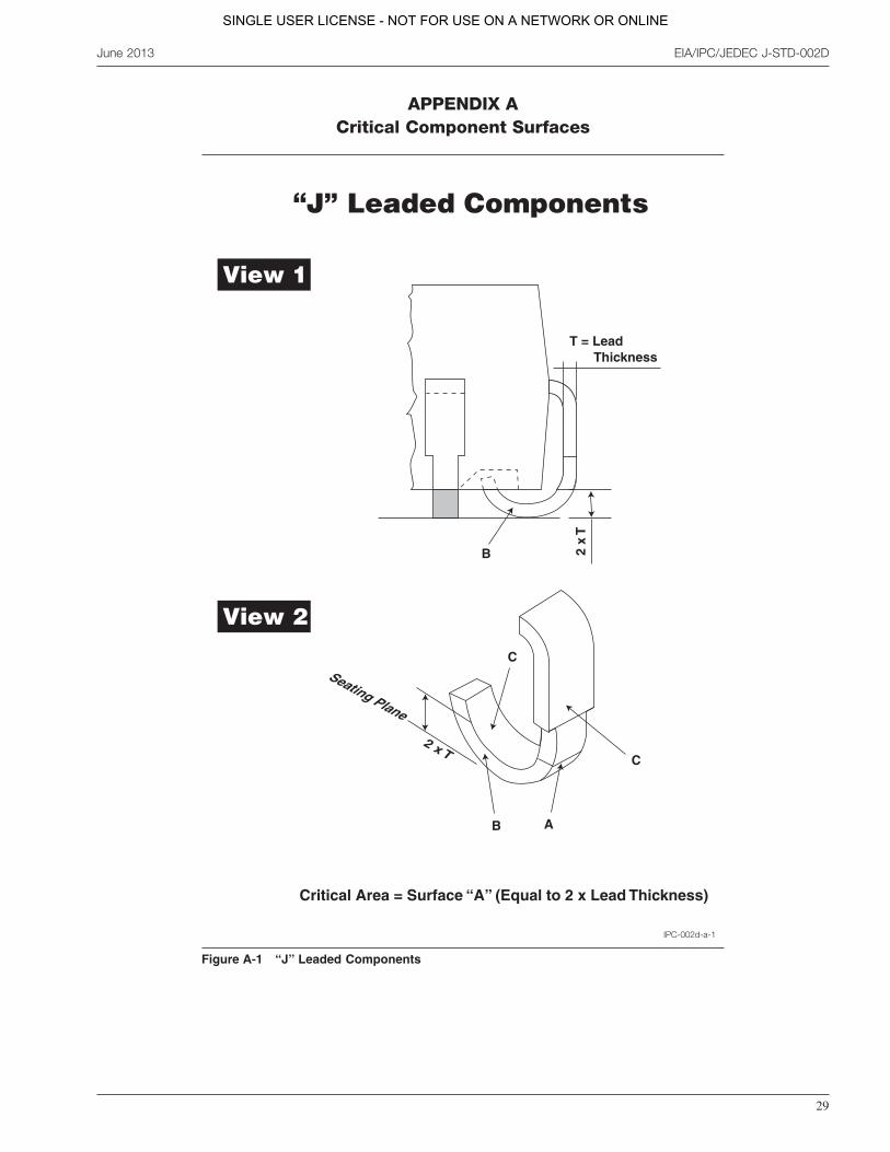
APPENDIX ACritical Component Surfaces
IPC-002d-a-1
Figure A-1 ‘‘J’’ Leaded Components
“J” Leaded Components
View 1
View 2
T = Lead
2 x
T
2 x T
Thickness
A
C
C
B
B
Critical Area = Surface “A” (Equal to 2 x Lead Thickness)
Seating Plane
June 2013 EIA/IPC/JEDEC J-STD-002D
29
SINGLE USER LICENSE - NOT FOR USE ON A NETWORK OR ONLINE

IPC-002d-a-2
Figure A-2 Passive Components
EIA/IPC/JEDEC J-STD-002D June 2013
30
SINGLE USER LICENSE - NOT FOR USE ON A NETWORK OR ONLINE

IPC-002d-a-3
Figure A-3 Gull Wing Components
Gull Wing Components
View 1
View 2
T = Lead
1 x
T
Thickness
A (Underside)B
B
Seating Plane
Seating Plane
1 x T
Critical Area = Surface “A” (Underside of Lead) up to 1 x T
June 2013 EIA/IPC/JEDEC J-STD-002D
31
SINGLE USER LICENSE - NOT FOR USE ON A NETWORK OR ONLINE

IPC-002d-a-4
Figure A-4 Leadless Chip Carrier
EIA/IPC/JEDEC J-STD-002D June 2013
32
SINGLE USER LICENSE - NOT FOR USE ON A NETWORK OR ONLINE

IPC-002d-a-5
Figure A-5 ‘‘L’’ Leaded Component
“L” Leaded Components
View 1
View 2
C
B Excluded
A (Underside)
F
H
T = Lead Thickness
Seating Plane
Seating Plane
1 x T
Critical Area = Surface “A” (Underside of Lead) up to 1 x T
H
F
F = Minimum Fillet Height = The Lesser of: a) The solder fillet thickness on the underside of the lead + 0.25 x H or b) 0.5mm [0.0197in].
June 2013 EIA/IPC/JEDEC J-STD-002D
33
SINGLE USER LICENSE - NOT FOR USE ON A NETWORK OR ONLINE

IPC-002d-a-6
Figure A-6 Exposed Pad Package
Critical Area = Surface A (Terminal Undersides) andSurface B (Exposed Pad)
C, Terminal Sides, not intended to be a wettable surface by design
A, Terminal Underside.Length L, Width W
B, Exposed Pad.Length L, Width W
Exposed Pad Package
IPC-002b-a-7
Figure A-7 Bottom-Only Termination Component
Critical Area = Surface A (Terminal Undersides)
A, Terminal Underside.Length L, Width W
B, Terminal Side, not intended to be a wettable surface by design
Bottom-OnlyTermination Component
EIA/IPC/JEDEC J-STD-002D June 2013
34
SINGLE USER LICENSE - NOT FOR USE ON A NETWORK OR ONLINE

IPC-002d-a-8
Figure A-8 Area Array Component Critical Surface
Area Array ComponentCritical Surface
Note: Critical Surface: Each solder sphere shall haveincorporated the solder paste deposit (uniform, smooth solderwith no dewetted areas). With Tests S and S1 - Surface MountProcess Simulation, the component leads shall be wetted in aconsistent and unified manner, with no evidence of surfaceoxidation anomalies.
June 2013 EIA/IPC/JEDEC J-STD-002D
35
SINGLE USER LICENSE - NOT FOR USE ON A NETWORK OR ONLINE

IPC-002d-a-9
Figure A-9 Through-Hole Components - Flat Pin
EIA/IPC/JEDEC J-STD-002D June 2013
36
SINGLE USER LICENSE - NOT FOR USE ON A NETWORK OR ONLINE

IPC-002b-a-7
Figure A-10 Through-Hole Components - Round Pin
June 2013 EIA/IPC/JEDEC J-STD-002D
37
SINGLE USER LICENSE - NOT FOR USE ON A NETWORK OR ONLINE

APPENDIX BEvaluation Aids
B.1 Evaluation Aids for Tests A, C, A1, and C1
B.2 Round Leads The measurement of defects or the estimation of defect area percentage of the lead total surface area,is more difficult with round leads than it is with flat surface rectangular leads. For example, in viewing a cylindrical surfacesuch as a round lead, a round diameter-sized defect when flat appears oval shaped and narrower in width than the visiblesurface of the lead in the transverse direction..
To aid the solderability test inspector in estimating the lead surface percentage after solderability testing, a guide sheet fordifferent diameter leads is shown in Figure B-3. When 25.4 mm [1.0 in] of the lead surface of a 0.5 mm [0.02 in] diameterlead is inspected for solder coverage, 10 diameter size defects equal 5% of the total lead surface area. Numbers of halfdiameter size and quarter diameter size defects are also listed. Combinations of these sizes can also be totaled easily (seeFigure B-1).
In considering areas not covered by a continuous, new solder coating and referring to the defined defects illustrated in Fig-ure B-2, the visible areas of dewetting and nonwetting are applicable directly.
An example of what constitutes 5% of the dipped area is: six defects of 0.813 mm [0.032 in] diameter in a 25.4 mm [1.0in] length of a 0.813 mm [0.032 in] diameter (No. 20 AWG) wires (see Figures B-3, B-4, and B-5).
IPC-002d-b-1
Figure B-1 Defect Size Aid
Bo
dy
Example "A"0.51 mm Dia.Size Area
0.51 mm Dia. Lead
On 0.51 mm Dia.Lead 25.4 mm of
Solder Coated Length
Example "B"1/2 of Dia.Size Area Example "C"
1/4 of Dia.Size Area
Total of 10 Example "A" Areas - 5% of Lead
Area
Total of 40 Example "B" Areas - 5% of Lead
Area
Total of 160 Example "C" Areas - 5% of Lead Area
EIA/IPC/JEDEC J-STD-002D June 2013
38
SINGLE USER LICENSE - NOT FOR USE ON A NETWORK OR ONLINE

B.3 Square Terminations Square terminations shall meet the requirements of the solderability coverage guide shown inFigure B-5.
B.4 Castellated Terminations Castellated terminations shall meet the same criterion as round leads.
IPC-002d-b-2a, b-2b, b-2c
Figure B-2 Types of Solderability Defects
a) Dewetting b) Nonwetting
c) Pinholes
June 2013 EIA/IPC/JEDEC J-STD-002D
39
SINGLE USER LICENSE - NOT FOR USE ON A NETWORK OR ONLINE

IPC-002d-b-3
Figure B-3 Aids in Evaluation of 5% Allowable Area of Pin Holes
TERMINAL_ROUND_LEAD
SCALE: 10XCRITICAL AREA 5% DEFECTIVE
AFTER THE MANNER OF MIL. STD. 202METHOD 208 FIGURE 208-7
20 UNITS OF 400 DISTRIBUTED RANDOMLY
.020 DIA X 1.00
.032 DIA X 1.00
.040 DIA X 1.00
REF: EIA 10X LEGEND: INVISIBLE TO OPPOSITE VISIBLE
CRITICAL AREA ENTIRE 25 mm LG. SURFACE STARTING AT 1.3 mm FROM BODY
EIA/IPC/JEDEC J-STD-002D June 2013
40
SINGLE USER LICENSE - NOT FOR USE ON A NETWORK OR ONLINE

IPC-002d-b-4
Figure B-4 Aid in Evaluation of 5% Allowable Area of Pin Holes
June 2013 EIA/IPC/JEDEC J-STD-002D
41
SINGLE USER LICENSE - NOT FOR USE ON A NETWORK OR ONLINE

IPC-002d-b-5
Figure B-5 Solderability Coverage Guide
3 Percent Defects
5 Percent Defects
8 Percent Defects
EIA/IPC/JEDEC J-STD-002D June 2013
42
SINGLE USER LICENSE - NOT FOR USE ON A NETWORK OR ONLINE

APPENDIX CCalculation of Maximum Theoretical Force
Maximum theoretical force is calculated using the procedure of Klein Wassink.1
Force (Max. Theoretical) = (γ) (P) (cosine β) - (d)(g)(V) = [0.4P - 0.08V] mN
where:
P = the perimeter of the test specimen in millimeters, i.e., the length in millimeters of the solder/printed board or couponpad (or hole)/air interface as measured at maximum depth of immersion.
V = The volume in cubic millimeters of the test specimen that resides below the solder/board air interface as measured atthe maximum depth of immersion.
γ = Surface tension of solder = 0.4 mN/mm
γ = Surface tension of Pb-free solder = 0.5 mN/mm
α = Immersion angle of the board to the horizontal surface, i.e., α = 45°
β = Wetting angle of solder to the board under optimal conditions, i.e., β = 0 and therefore the cosine β = 1
d = Density of solder at 245°C = 8110 kg/m3 for Sn60/Pb40 Alloy or
d = Density of solder at 245°C = 8020 kg/m3 for Sn60/Pb40 Alloy or
d = Density of solder at 245°C = 7.41 kg/m3 for SAC305 Alloy
g = Gravitational constant = 9.8 x 103 mm/s2
Periphery and volumes are to be calculated using the nominal values provided by the device supplier in the package draw-ing and the angles and depths of immersion as described in the specification above. The TOTAL periphery and volume, i.e.,the sum of all leads being immersed, is to be used in this calculation.
Figure C-1 below depicts a sample calculation for 132 I/O QFP.
IPC-002d-c-1
Figure C-1 Lead Periphery and Volume for a 132 I/O PQFP
Solder Bath Surafce
t=0.1524w=0.254
d
m
k
l
June 2013 EIA/IPC/JEDEC J-STD-002D
43
SINGLE USER LICENSE - NOT FOR USE ON A NETWORK OR ONLINE

Where:
w = Lead width (nominal) = 0.254 mm
t = Lead height (nominal) = 0.1524 mm
d = Immersion depth = 0.3 mm
1 = Lead length immersed on bottom side at 20° angle and 0.3 mm depth = 0.877 mm
m = Lead length immersed on top side at 20° angle and 0.3 mm depth = 0.458 mm
k = Length of solder/lead/air interface along lead side = 0.446 mm
2k + 2w = Total length per lead of solder periphery = 0.892 + 0.508 = 1.4 mm
P = Total length of periphery per side (33 leads) = 46.2 mm
Hence:
Total volume immersed per lead = 0.254 X 0.1524 X 0.458 + 0.5(0.1524 X 0.254 X 0.419) = 0.0177 + 0.0081 =0.0258 mm3
Therefore for an 132 I/O QFP, the maximum theoretical wetting force is:
For 33 leads (one side of an 132 I/O QFP) = 33 x 0.0258 mm3 = 0.85
Maximum Force = (0.4 x 46.2) - (0.08 x 0.85) = 18.41 mN
And, for a part of 46.2 mm total periphery:
Maximum Force per length of interface = 399 µN/mm
The force measured on a part in the Set A criteria must therefore be greater than 9.2 mN or 200 µN/mm at F2.
Note: All forces are referenced to the corrected zero axis and not the zero force line except for the Appendix Dcalculation (parameter AA).
1. R. J. Klein Wassink, ‘‘Soldering in Electronics,’’ 2nd Edition, Electrochemical Publications, Ayr, Scotland, 1989,pp 308-309
EIA/IPC/JEDEC J-STD-002D June 2013
44
SINGLE USER LICENSE - NOT FOR USE ON A NETWORK OR ONLINE

APPENDIX DCalculation of Integrated Value of Area of the Wetting Curve
The area is calculated using the maximum theoretical force (see Figure 4.18 or 4.19). Therefore, the area is given as:
Area = (Wetting force x Time) - (Buoyancy x Time)Area = (3.0 sec. x Max. Theoretical Force) - 2.0 sec (ρ ) (g) VArea = (3.0 sec. x Max. Theoretical Force) - 2.0 sec x - (8.12 x 10⁻⁶ kg/mm3 x 9.8 x 103 mm/s2 x V)
The value V is the volume of the test specimen immersed in the solder bath as calculated in Appendix C. The maximumtheoretical force is calculated as per Appendix C. The following assumptions are made:
1. The maximum buoyancy force holds for the whole two (2) seconds contributing a negative area of: the buoyancy forcetimes 2 seconds.
2. The test specimen essentially attains the full maximum theoretical force as it crosses the zero line at 2 seconds and holdsthat value for the duration of the test, i.e., 3 seconds.
V = Total Volume = 0.4 mm3
Maximum Theoretical Force = 3.97 mN
Area = (3.0 sec. x 3.97mN) - (2.0 sec. x 0.08 (kg/mm3 x mm/s2) x 0.4 mm3) = 11.91 mN x seconds - 0.064 (kg-mm/sec)
Since F = ma, then mN = kg x mm/sec2 or kg = mNsec2/mm
Area = 11.91 mN x seconds - 0.064 (mNsec2/mm) x (mm/sec)Area = 11.91 mN x seconds - 0.064 mN x secondsArea = 11.85 mN x seconds
June 2013 EIA/IPC/JEDEC J-STD-002D
45
SINGLE USER LICENSE - NOT FOR USE ON A NETWORK OR ONLINE

APPENDIX EInformative Annex
E.1 TEST EQUIPMENT SOURCES
The equipment sources described below represent those currently known to the industry. Users of this document are urgedto submit additional source names as they become available, so that this list can be kept as current as possible.
E.1.1 Tests A, B, C, D, A1, B1, C1, and D1
GEN3 Systems Limited (Formerly Concoat Systems) Unit B2, Armstrong Mall, Southwood Business Park, Farnborough,Hampshire GU14 0NR England. 011 44 12 5252 1500 www.gen3systems.comHMP Soldermatics, P.O. Box 948, Canon City, CO 81215, (719) 275-1531Malcomtech 26200 Industrial Blvd, Hayward CA 64545, (510)293-0580, www.malcomtech.comReef Engineering, Unit 6, Bancrofts Road, South Woodham Ferrers, Essex CM3 5UQ 01245 328123Robotic Process Systems Inc., 23301 E. Mission Ave., Liberty Lake, WA 99019, (509)891-1680
E.1.2 Tests E, F, E1 and F1
Convey AB, Harpsundsvagen 113, S-12458 Bandhagen, Sweden 46 (0) 8 99 66 25GEN3 Systems Limited (Formerly Concoat Systems) Unit B2, Armstrong Mall, Southwood Business Park, Farnborough,Hampshire GU14 0NR England. 011 44 12 5252 1500 www.gen3systems.comMalcomtech 26200 Industrial Blvd, Hayward CA 64545, (510) 293-0580, www.malcomtech.comMetronelec, 54, Route de Sartrouville - Le Montreal 78232 Le PECO Cedex, France (USA Distributor: Solderability Test-ing and Solutions Inc., 108 Rosedale ave, Richmond KY 40475, (859) 353-5914, www.standsgroup.comRobotic Process Systems Inc., 23301 E. Mission Ave., Liberty Lake, WA 99019, (509)891-1680
E.1.3 Tests G and G1
GEN3 Systems Limited (Formerly Concoat Systems) Unit B2, Armstrong Mall, Southwood Business Park, Farnborough,Hampshire GU14 0NR England. 011 44 12 5252 1500 www.gen3systems.comMetronelec, 54, Route de Sartrouville - Le Montreal 78232 Le PECO Cedex, France (USA Distributor: Solderability Test-ing and Solutions Inc., 108 Rosedale ave, Richmond KY 40475, (859) 353-5914, www.standsgroup.com
E.1.4 Steam Conditioning Equipment
H&H Engineering, Inc., 3612 Wood Duck Circle, Stockton, CA 95206Metronelec, 54, Route de Sartrouville - Le Montreal 78232 Le PECO Cedex, France (USA Distributor: Solderability Test-ing and Solutions Inc., 108 Rosedale ave, Richmond KY 40475, (859) 353-5914, www.standsgroup.comMountaingate Engineering Inc., Campbell, CA 95008, (408) 866-5100Robotic Process Systems Inc., 23301 E. Mission Ave., Liberty Lake, WA 99019, (509) 891-1680Zentek Scientific Systems, 3520 Yale Way, Fremont, CA 94538, (510) 651-1581
E.1.5 Grid Reticles
Bender Associates, 5030 South Mill Avenue, Suite C-2, Tempe, AZ 85252, (602) 820-0900
E.2 TEST FLUX PRODUCT SOURCES
The Test Flux product sources described below represent those currently known to the industry. Users of this document areurged to submit additional product source names as they become available, so that this list can be kept as current as possible.AIM Solder www.aimsolder.com - Standard Flux #1 Product ID: RMA 202-25Alpha Metals www.alphametals.com - Standard Flux #2GEN3 Systems Limited www.gen3systems.com - Product ID’s: SMNA - Standard Flux #1: Actiec 2 / - Standard Flux #2:Actiec 5Kester www.kester.com - Standard Flux #1 Product ID: 182Qualitek International, Inc. www.qualitek.com - Standard Flux #1Product ID: 285-25Solderability Testing and Solutions Inc. www.wettingbalance.com - Standard test flux 0.2% and Standard test flux 0.5%Ascentech LLC, 127 Goose Hill Rd, Chester CT 06412, tel = 860-526-8903, flux 1 & 2Revise ST and S, 108 Rosedale Ave, Richmond KY 40475, tel = 8593535914, www.standsgroup.com, flux 1 & 2
EIA/IPC/JEDEC J-STD-002D June 2013
46
SINGLE USER LICENSE - NOT FOR USE ON A NETWORK OR ONLINE

APPENDIX FJ-STD-002/J-STD-003 Activated Solderability
Test Flux Rationale Committee Letter
The current J-STD-002/J-STD-003 specification includes a departure in the test flux methodology used in past solderabilitytesting. The table in 3.2.2 Flux is:
The J-STD-002/J-STD-003 committees understood that any proposed change to the use of ROL0 (formerly designated typeR) would be heavily scrutinized and would require test data showing the applicability of using a standard activated fluxcomposition. The J-STD-002/J-STD-003 committees have spent significant resources working this flux change issue, dis-cussing the chemistry details and conducting multi-company Design of Experiment investigations. The J-STD-002 commit-tee chairmen, Dave Hillman [Rockwell Collins], Doug Romm [Texas Instruments], Mark Kwoka [Intersil] and Jack McCul-len [Intel], feel that the committee has compiled a significant data set and have held thorough topic discussions supportingthe proposed flux material change. The four rationales for proposing/supporting the flux change are summarized below:
1) A Proactive Solderability Testing Approach To The Implementation of Non-Tin Finishes
A number of industry studies (1996 NEMI Surface Finishes Task Group Report, 1997 NCMS Pb-free Solder Project,2000 National Physical Laboratory CMMT (A) 284 Report) have shown that an incompatibility of ‘‘R type’’ flux withnon-tin surface finishes such as palladium, organic solderability preservatives (OSPs), and immersion gold. The intro-duction of these various metallic surface finishes on components and printed wiring boards is no longer the exceptionbut has/is quickly becoming the norm. The use of a ‘‘R type’’ flux containing only naturally occurring activators hasresulted in producing ‘‘false negative’’ solderability test results which impact both the component/board fabricator andthe assembler negatively in terms of cost and schedule.
2) Reduced Solderability Test Variability
The J-STD-002/003 solderability committees enlisted the assistance of Dr. Carol Handwerker and the resources of theNational Institute of Standards & Technology (NIST) to investigate/compare a standard activated flux composition ver-sus the ‘‘R type’’ flux composition. A detailed statistical analysis by Bill Russell [Raytheon Systems] and NIST statis-ticians revealed the use of a standard activated flux composition greatly reduced the amount of solderability test varia-tion. One of the major goals of the J-STD-002/003 solderability committees is to develop test methods and standardswhich promote consistency across the industry.
3) Concerns of A Loss of Solderability Assessment Safety Margin
The two major historical rationale for using an ‘‘R type’’ flux: 1) colophony or rosin contains only naturally occurringflux activator constituents and thus is not subjected to the problems/complications of chemistry formulas by the fluxsupplier; 2) it was an accepted industry acknowledged fact that, if a component or printed wiring board surface wasfound to have acceptable solderability test results using ‘‘R type’’ flux, then the more active flux formulations used inthe assembly process would produce acceptable solder process results. This solderability assessment safety margin wasa self-imposed, industry consensus decision. The J-STD-002/003 committees understood the historical relevance behindthe decision to use ‘‘R type’’ flux and had an equally strong desire to maintain a solderability assessment safety cush-ion. However, committees fielded a number of industry inputs to reassess the solderability flux composition based onthe technology improvements in surface finishes, improvements in the flux chemistry formulations from flux suppliers,and the desire to not have excessive safety margins which would impact cost and schedule in a non-value added man-ner. The committees conducted a number of tests (Wenger, Kwoka, ACI) demonstrating, using a specific standard levelof activation on real world, industry supplied component and printed wiring board cases, that the occurrence of a ‘‘falseacceptable’’ solderability test result was extremely low. There was no case that exhibited a ‘‘pass ROL1 test - fail ROL0
Table 3-1 Flux Compositions
Constituent
Composition by Weight Percent
Flux #1 Flux #2
Colophony 25 ± 0.5 25 ± 0.5
Diethylammonium Hydrochloride (CAS 660-68-4) 0.15 ± 0.01 0.39 ± 0.01
Isopropyl Alcohol (IPA) (CAS 67-63-0) Balance Balance
Weight of Chlorine as % of Solids 0.2 0.5
June 2013 EIA/IPC/JEDEC J-STD-002D
47
SINGLE USER LICENSE - NOT FOR USE ON A NETWORK OR ONLINE

test - Fail during board assembly’’ sequence. In fact, the use of both ROL1 and ROL0 are more likely to create a ‘‘falsereject ‘‘dip and look solderability test result when compared to board level soldering performance.
4) Standardization of Solderability Test Flux Composition On A Global Scale
A second major goal of the J-STD-002/003 solderability committees is to develop test methods and standards whichpromote global standardization for the electronics industry. The standard activated flux composition selected and testedby the committees has been utilized in the International Electrotechnical Commission (IEC) 60068-2-20 Solderingspecification. The IEC specification is successfully utilized for solderability testing. Having compatibility of flux com-position requirements between the J-STD-002/003 specification and the IEC specifications is a win-win situation forelectronics assemblers and component/printed wiring board fabricators.
A number of the major flux chemistry suppliers have been queried on the electronics industry’s ability to purchase the stan-dard activated flux composition, and a positive response was received. If you have any questions please contact the IPCTechnical Staff to obtain additional answers/clarification.
EIA/IPC/JEDEC J-STD-002D June 2013
48
SINGLE USER LICENSE - NOT FOR USE ON A NETWORK OR ONLINE

APPENDIX GGraphical Representations: Progression of Solder Wetting Curve
Parameters As Measured By Wetting Balance Testing
Time 0
Force (mN)
BuoyancyTime (s)
F1
0T1
F2
T2
Understanding Wetting Curves
Time 0
Force (mN)
BuoyancyTime (s)
F1
0T1
F2
T2
Understanding Wetting Curves
June 2013 EIA/IPC/JEDEC J-STD-002D
49
SINGLE USER LICENSE - NOT FOR USE ON A NETWORK OR ONLINE

Time 0 Ta
Force (mN)
BuoyancyTime (s)
F1
Ta
0T1
F2
T2
Understanding Wetting Curves
Time 0 Ta
Force (mN)
BuoyancyTime (s)
F1
Ta Tb
0T1
F2
T2
Understanding Wetting Curves
Tb
EIA/IPC/JEDEC J-STD-002D June 2013
50
SINGLE USER LICENSE - NOT FOR USE ON A NETWORK OR ONLINE
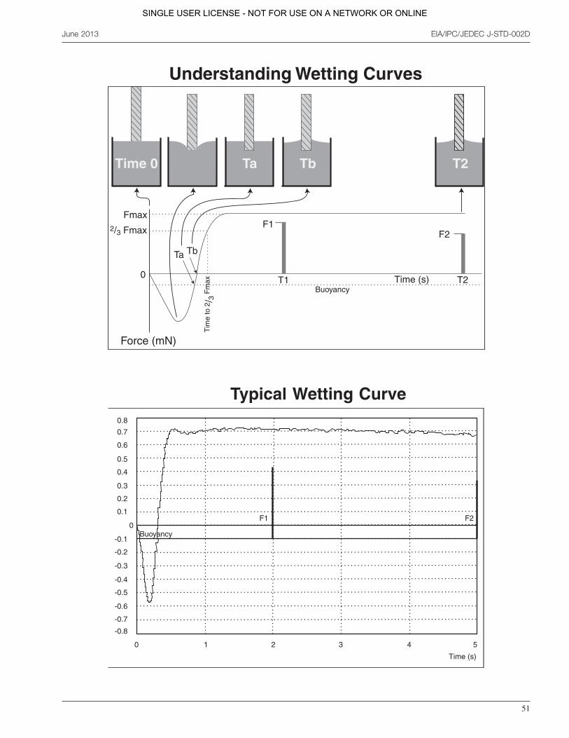
Time 0 Ta
Force (mN)
BuoyancyTime (s)
F1
Ta Tb
0
Fmax2/3 Fmax
Tim
e to
2/ 3
Fm
ax
T1
F2
T2
Understanding Wetting Curves
Tb T2
Typical Wetting Curve
Buoyancy
Time (s)
0.8
0.7
0.6
0.5
0.4
0.3
0.2
0.1
0
-0.1
-0.2
-0.3
-0.4
-0.5
-0.6
-0.7
-0.8
0 1 2
F1 F2
3 4 5
June 2013 EIA/IPC/JEDEC J-STD-002D
51
SINGLE USER LICENSE - NOT FOR USE ON A NETWORK OR ONLINE

APPENDIX HTest Protocol for Wetting Balance Gauge Repeatability and
Reproducibility (GR&R) Using Copper Foil Coupons
1. All coupons for these tests shall be prepared individually just prior to testing. Do NOT batch clean thesamples.
2. Copper foil of 35 microns nominal thickness (‘‘1 oz.’’ copper) shall be used for the test.
3. The copper foil shall have NO surface treatment and is expected to have an oxidized appearance uponreceipt from the supplier. Do not use the copper foil if it is bright and shiny. This is indicative of surface antitarnish treatments being used. Surface treatments / preservatives can interfere with the ability to make aconsistent ‘‘known good coupon’’ necessary for this test.
4. The copper foil coupons shall be die cut to ensure repeatability of the samples being tested and shall be ofthe following width dimensions;
a. 2 mm
b. 5 mm
c. 10 mm
5. Create a file for each foil width and for each individual person that is involved performing the GR&R.
6. Test parameters shall be:
a. Solder temperature shall be the as recommended for the alloy and the specification being used (i.e., forSnPb and ANSI-J-STD-003), it shall be 235 °C, for ANSI-J-STD-002, it shall be 245 °C. For SAC 305, itshall be 255 °C, regardless of the specification.
b. Immersion depth shall be 0.4 mm.
c. Immersion speed shall be 2 mm/sec.
d. Dwell time in the solder shall be 10 seconds.
e. Immersion angle shall be 90 degrees incident to the solder.
f. No preheat shall be used.
7. Sample preparation for the ‘‘known good coupon’’ shall be as follows:
a. Use a tweezers to immerse a foil sample into a beaker of acetone and gently agitate for 20 seconds.
b. Remove sample and blot both sides dry with lint free cloth or other suitable lab tissue.
c. Again using a tweezers, immerse the above sample into a 20% v/v nitric acid/DI water solution andgently agitate for 20 seconds.
d. Immerse the sample immediately into DI water and gently agitate for 20 seconds.
e. Blot the sample dry as in step ‘‘b’’ above.
8. Dip sample into the ‘‘standard activated flux’’ normally used for solderability testing for 5 seconds.
9. Holding the samples vertically, blot to remove excess flux.
10. Place sample into tool holder.
11. Run the test.
12. Repeat ten times for each foil width and each test person. It is recommended that three people should be used for theGR&R study.
13. For ease of data manipulation, it is recommended to convert the wetting forces obtained into mN/mm of the coupon’swettable length (perimeter). For example, the 10 mm wide coupon has a total wettable length (perimeter) = [(2 x10 mm) + (2 x 0.035 mm)] = 20.07 mm.
14. For the ‘‘standard activated’’ flux of nominal 0.2% activation, the wetting force used for the calculations shall be0.31 mN/mm. If a more active flux is being used, a large sample shall be run to obtain the mean value and this usedfor the calculations.
EIA/IPC/JEDEC J-STD-002D June 2013
52
SINGLE USER LICENSE - NOT FOR USE ON A NETWORK OR ONLINE

15. Calculate the standard deviation for each of the foil widths and the people running the test.
16. Multiply the standard deviation value by 6 (this represents the plus - minus 3 standard deviations of a normaldistribution).
17. Divide this number by 0.31 and multiply by 100 to obtain a percentage value.
18. Tabulate the three values per person.
19. For an acceptable GR&R, the values obtained should be below 10%.
20. There should be excellent R&R results with the 10 mm coupon the first time this protocol is performed with an increas-ing spread from test person to test person when using the smaller coupons. The test may need to be repeated or indi-viduals may require some ‘‘practice time’’ prior to running the full GR&R.
21. In addition to testing the individual, this protocol also tests the machine and will show linearity and any bias if it exists.Because the wetting forces have been normalized to mN/mm, the readings for each coupon width should be the same.If they are clearly different but the standard deviations produced by the individual test people are below 10%, then thereis a problem with the wetting balance and the equipment manufacturer should be notified.
June 2013 EIA/IPC/JEDEC J-STD-002D
53
SINGLE USER LICENSE - NOT FOR USE ON A NETWORK OR ONLINE

This Page Intentionally Left Blank
EIA/IPC/JEDEC J-STD-002D June 2013
54
SINGLE USER LICENSE - NOT FOR USE ON A NETWORK OR ONLINE

Standard Improvement Form EIA/IPC/JEDEC J-STD-002DThe purpose of this form is to provide theTechnical Committee of IPC with inputfrom the industry regarding usage ofthe subject standard.
Individuals or companies are invited tosubmit comments to IPC. All commentswill be collected and dispersed to theappropriate committee(s).
If you can provide input, please completethis form and return to:
IPC3000 Lakeside Drive, Suite 309SBannockburn, IL 60015-1249Fax 847 615.7105E-mail: [email protected]
1. I recommend changes to the following:
Requirement, paragraph number
Test Method number , paragraph number
The referenced paragraph number has proven to be:
Unclear Too Rigid In Error
Other
2. Recommendations for correction:
3. Other suggestions for document improvement:
Submitted by:
Name Telephone
Company E-mail
Address
City/State/Zip Date
SINGLE USER LICENSE - NOT FOR USE ON A NETWORK OR ONLINE

847-615-7100 tel 847-615-7105 fax www.ipc.org
3000 Lakeside Drive, Suite 309 SBannockburn, IL 60015
Association Connecting Electronics Industries
®
ISBN #978-1-61193-089-4
SINGLE USER LICENSE - NOT FOR USE ON A NETWORK OR ONLINE