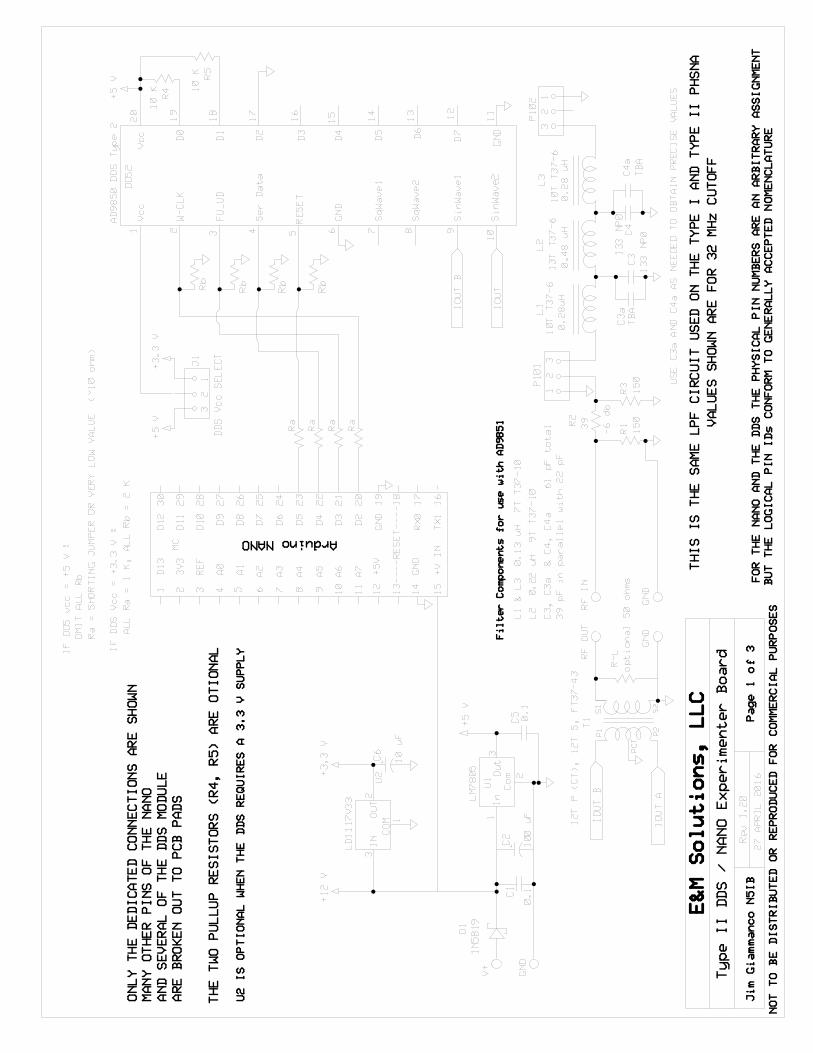
dds type-2 and arduino nano experimenter board type-2 arduino nano... · 2018-04-14 · dds type-2...
TRANSCRIPT
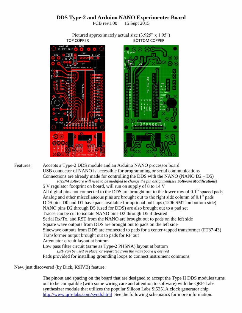
DDS Type-2 and Arduino NANO Experimenter Board PCB rev1.00 15 Sept 2015
Pictured approximately actual size (3.925” x 1.95”)
TOP COPPER BOTTOM COPPER
Features: Accepts a Type-2 DDS module and an Arduino NANO processor board
USB connector of NANO is accessible for programming or serial communications
Connections are already made for controlling the DDS with the NANO (NANO D2 – D5) PHSNA software will need to be modified to change the pin assignment(see Software Modifications) 5 V regulator footprint on board, will run on supply of 8 to 14 V
All digital pins not connected to the DDS are brought out to the lower row of 0.1” spaced pads
Analog and other miscellaneous pins are brought out to the right side column of 0.1” pads
DDS pins D0 and D1 have pads available for optional pull-ups (1206 SMT on bottom side)
NANO pins D2 through D5 (used for DDS) are also brought out to a pad set
Traces can be cut to isolate NANO pins D2 through D5 if desired
Serial Rx/Tx, and RST from the NANO are brought out to pads on the left side
Square wave outputs from DDS are brought out to pads on the left side
Sinewave outputs from DDS are connected to pads for a center-tapped transformer (FT37-43)
Transformer output brought out to pads for RF out
Attenuator circuit layout at bottom
Low pass filter circuit (same as Type-2 PHSNA) layout at bottom LPF can be used in place, or separated from the main board if desired
Pads provided for installing grounding loops to connect instrument commons
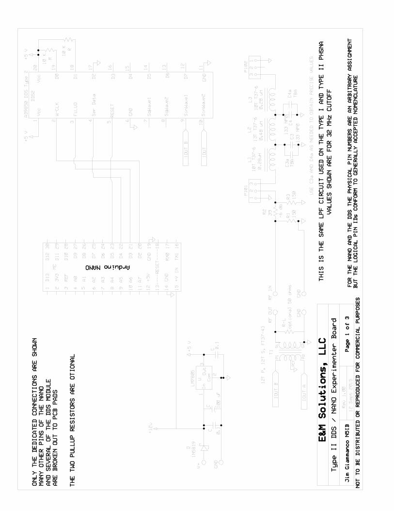
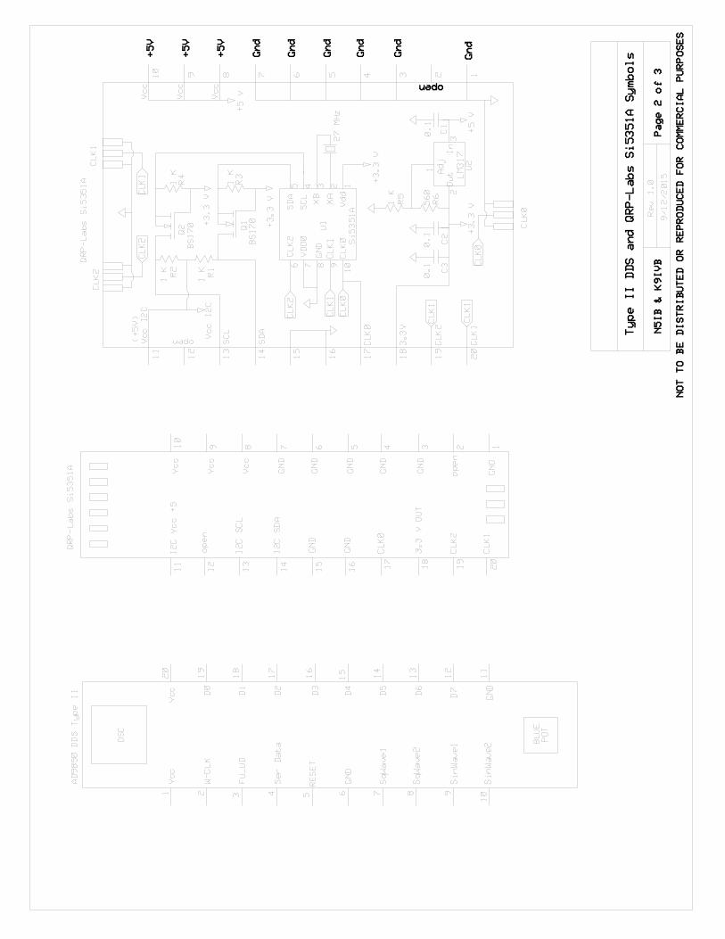
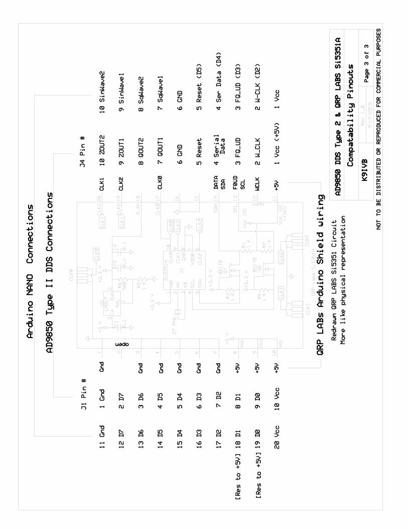
New, just discovered (by Dick, K9IVB) feature:
The pinout and spacing on the board that are designed to accept the Type II DDS modules turns
out to be compatible (with some wiring care and attention to software) with the QRP-Labs
synthesizer module that utilizes the popular Silicon Labs Si5351A clock generator chip
http://www.qrp-labs.com/synth.html See the following schematics for more information.
Building and Application notes (more to come)
The key to getting the Arduino NANO and a Type II DDS module to “piggyback” is the selection of pins and
sockets for connecting the three circuit boards.
A DRY FIT TEST IS AN ABSOLUTE NECCESSITY TO MAKE SURE THERE WILL BE ENOUGH
CLEARANCE. DO THE DRY FIT BEFORE SOLDERING ANYTHING.
Many NANOs come with the header pins supplied, but not yet installed. That’s the kind you want to obtain,
since you will want to use a different type of pin strip than the one supplied. Most of the Type II DDS modules
already have the pin header strips installed. We have to work with what we have.
First we’ll deal with the NANO. The goal is to cozy
it up as close to the top surface of the PC board as
possible, without touching. To do this we’ll use
those breakaway strips of machined pins and
sockets. They are available at the usual parts houses,
or from eBay vendors. The tinned ones are fine – no
need to splurge on the gold plated ones.
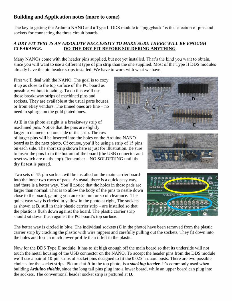
At E in the photo at right is a breakaway strip of
machined pins. Notice that the pins are slightly
larger in diameter on one side of the strip. The row
of larger pins will be inserted into the holes on the Arduino NANO
board as in the next photo. Of course, you’ll be using a strip of 15 pins
on each side. The short strip shown here is just for illustration. Be sure
to insert the pins from the bottom of the board (the USB connector and
reset switch are on the top). Remember – NO SOLDERING until the
dry fit test is passed.
Two sets of 15-pin sockets will be installed on the main carrier board
into the inner two rows of pads. As usual, there is a quick easy way,
and there is a better way. You’ll notice that the holes in these pads are
larger than normal. That is to allow the body of the pins to nestle down
close to the board, gaining you an extra mm or so of clearance. The
quick easy way is circled in yellow in the photo at right, The sockets –
as shown at B, still in their plastic carrier strip – are installed so that
the plastic is flush down against the board. The plastic carrier strip
should sit down flush against the PC board’s top surface.
The better way is circled in blue. The individual sockets (C in the photo) have been removed from the plastic
carrier strip by cracking the plastic with wire nippers and carefully pulling out the sockets. They fit down into
the holes and form a much lower profile than if left in the plastic.
Now for the DDS Type II module. It has to sit high enough off the main board so that its underside will not
touch the metal housing of the USB connector on the NANO. To accept the header pins from the DDS module
we’ll use a pair of 10-pin strips of socket pins designed to fit the 0.025” square posts. There are two possible
choices for the socket strips. Pictured at A in the top photo, is a stacking header. It’s commonly used when
building Arduino shields, since the long tail pins plug into a lower board, while an upper board can plug into
the sockets. The conventional header socket strip is pictured at D.
A C
B
D
E
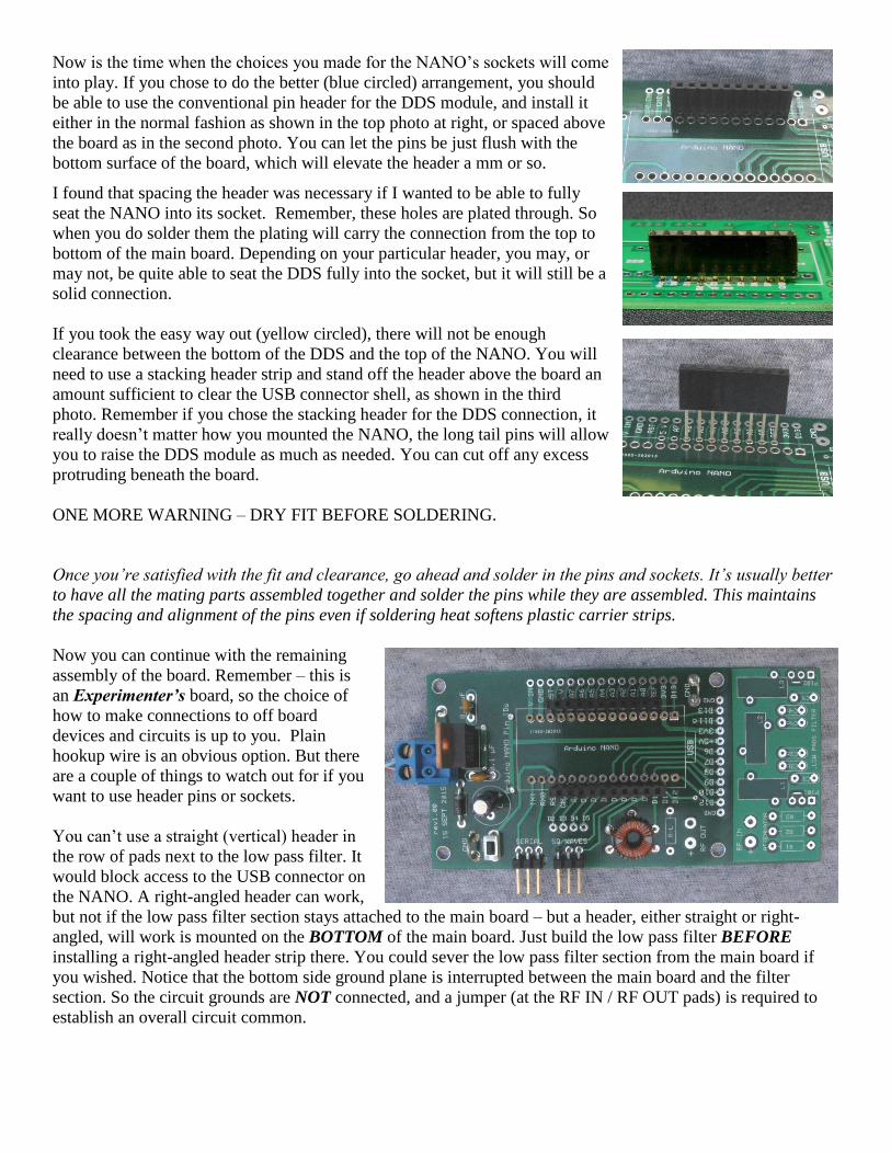
Now is the time when the choices you made for the NANO’s sockets will come
into play. If you chose to do the better (blue circled) arrangement, you should
be able to use the conventional pin header for the DDS module, and install it
either in the normal fashion as shown in the top photo at right, or spaced above
the board as in the second photo. You can let the pins be just flush with the
bottom surface of the board, which will elevate the header a mm or so.
I found that spacing the header was necessary if I wanted to be able to fully
seat the NANO into its socket. Remember, these holes are plated through. So
when you do solder them the plating will carry the connection from the top to
bottom of the main board. Depending on your particular header, you may, or
may not, be quite able to seat the DDS fully into the socket, but it will still be a
solid connection.
If you took the easy way out (yellow circled), there will not be enough
clearance between the bottom of the DDS and the top of the NANO. You will
need to use a stacking header strip and stand off the header above the board an
amount sufficient to clear the USB connector shell, as shown in the third
photo. Remember if you chose the stacking header for the DDS connection, it
really doesn’t matter how you mounted the NANO, the long tail pins will allow
you to raise the DDS module as much as needed. You can cut off any excess
protruding beneath the board.
ONE MORE WARNING – DRY FIT BEFORE SOLDERING.
Once you’re satisfied with the fit and clearance, go ahead and solder in the pins and sockets. It’s usually better
to have all the mating parts assembled together and solder the pins while they are assembled. This maintains
the spacing and alignment of the pins even if soldering heat softens plastic carrier strips.
Now you can continue with the remaining
assembly of the board. Remember – this is
an Experimenter’s board, so the choice of
how to make connections to off board
devices and circuits is up to you. Plain
hookup wire is an obvious option. But there
are a couple of things to watch out for if you
want to use header pins or sockets.
You can’t use a straight (vertical) header in
the row of pads next to the low pass filter. It
would block access to the USB connector on
the NANO. A right-angled header can work,
but not if the low pass filter section stays attached to the main board – but a header, either straight or right-
angled, will work is mounted on the BOTTOM of the main board. Just build the low pass filter BEFORE
installing a right-angled header strip there. You could sever the low pass filter section from the main board if
you wished. Notice that the bottom side ground plane is interrupted between the main board and the filter
section. So the circuit grounds are NOT connected, and a jumper (at the RF IN / RF OUT pads) is required to
establish an overall circuit common.
Software modifications
See the PHSNA Yahoo Group for more information about software
https://groups.yahoo.com/neo/groups/PHSNA/info
If you wish to construct a version of the Poor Ham’s Scalar Network Analyzer (PHSNA) using the
Experimenter Board, you can use the either the Terminal or Windows Versions of Nick’s (WA5BDU) software
that’s posted on the Yahoo Group, but it will be necessary to change the four lines of code that assign Arduino
pin numbers to the DDS control lines.
In either PHSNA_standard_rev_3r02.ino (the Terminal Version) or PHSNA_VB.ino (the Windows Version)
Locate these lines of code – the lines to be changed are in BOLDFACE:
#define NICK 0 // Special compile modes just for me -- set to zero for general distribution 1r10
#if NICK
#define DATA 11 // ***** NRK ONLY BAD PIN 8 USE 11 *******
#else
#define DATA 8 // for the rest of the world: Pin 8 - connect to serial data load pin (DATA or D7)
#endif
#define W_CLK 9 // Pin 9 - connect to AD9850 module word load clock pin (CLK)
#define FQ_UD 10 // Pin 10 - connect to freq update pin (FQ)
#define RESET 11 // Pin 11 - connect to reset pin (RST)
#define LEDpin 13 // Pin 13 - on board LED to be used as "heartbeat"
Edit the code to as shown below (the changed lines are, again, in BOLDFACE)
#define NICK 0 // Special compile modes just for me -- set to zero for general distribution 1r10
#if NICK
#define DATA 11 // ***** NRK ONLY BAD PIN 8 USE 11 *******
#else
#define DATA 4 // for the rest of the world: Pin 4 - connect to serial data load pin (DATA or D7)
#endif
#define W_CLK 2 // Pin 2 - connect to AD9850 module word load clock pin (CLK)
#define FQ_UD 3 // Pin 3 - connect to freq update pin (FQ)
#define RESET 5 // Pin 5 - connect to reset pin (RST)
#define LEDpin 13 // Pin 13 - on board LED to be used as "heartbeat"
No other software changes are needed.
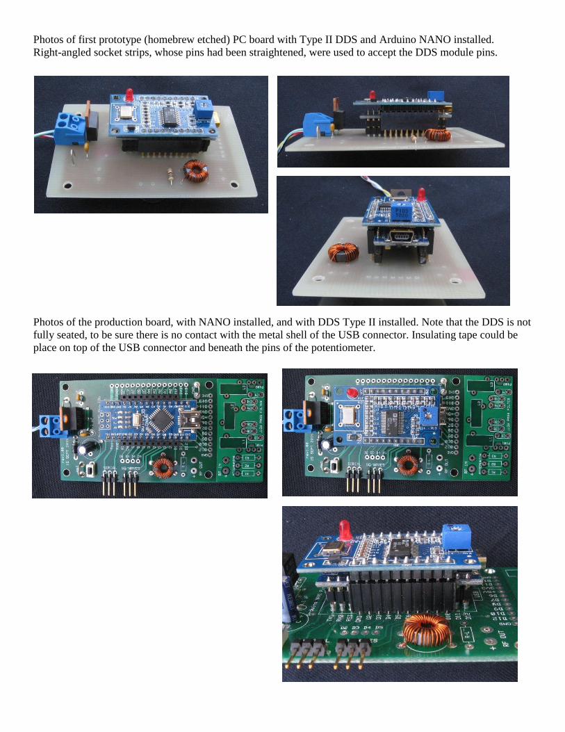
Photos of first prototype (homebrew etched) PC board with Type II DDS and Arduino NANO installed.
Right-angled socket strips, whose pins had been straightened, were used to accept the DDS module pins.
Photos of the production board, with NANO installed, and with DDS Type II installed. Note that the DDS is not
fully seated, to be sure there is no contact with the metal shell of the USB connector. Insulating tape could be
place on top of the USB connector and beneath the pins of the potentiometer.
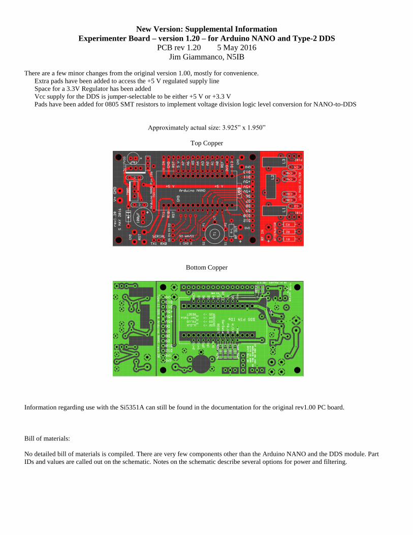
New Version: Supplemental Information
Experimenter Board – version 1.20 – for Arduino NANO and Type-2 DDS
PCB rev 1.20 5 May 2016
Jim Giammanco, N5IB
There are a few minor changes from the original version 1.00, mostly for convenience.
Extra pads have been added to access the +5 V regulated supply line
Space for a 3.3V Regulator has been added
Vcc supply for the DDS is jumper-selectable to be either +5 V or +3.3 V
Pads have been added for 0805 SMT resistors to implement voltage division logic level conversion for NANO-to-DDS
Approximately actual size: 3.925” x 1.950”
Top Copper
Bottom Copper
Information regarding use with the Si5351A can still be found in the documentation for the original rev1.00 PC board.
Bill of materials:
No detailed bill of materials is compiled. There are very few components other than the Arduino NANO and the DDS module. Part
IDs and values are called out on the schematic. Notes on the schematic describe several options for power and filtering.
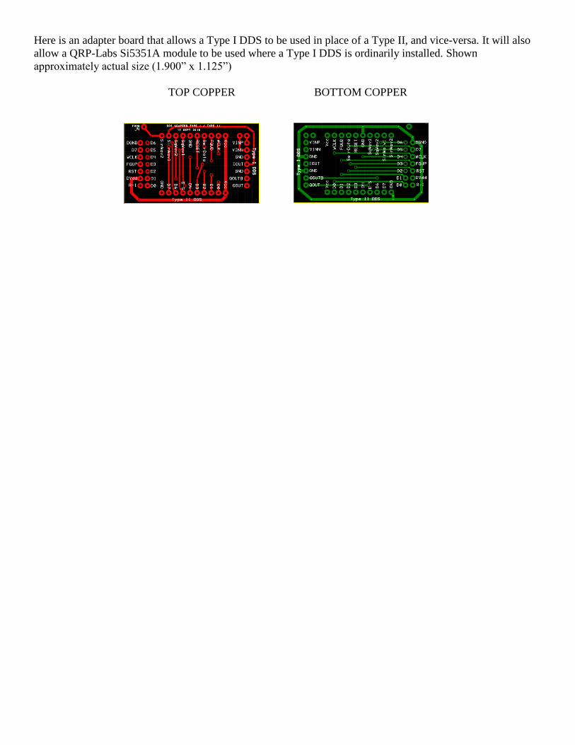
Here is an adapter board that allows a Type I DDS to be used in place of a Type II, and vice-versa. It will also
allow a QRP-Labs Si5351A module to be used where a Type I DDS is ordinarily installed. Shown
approximately actual size (1.900” x 1.125”)
TOP COPPER BOTTOM COPPER