dc power flow controller and marx dc-dc converter for...
TRANSCRIPT

DC Power Flow Controller
and Marx DC-DC Converter
for Multiterminal HVDC System
Etienne Veilleux
Department of Electrical & Computer EngineeringMcGill UniversityMontreal, Canada
A thesis submitted to McGill University in partial fulfillment ofthe requirements for the degree of Doctor of Philosophy.
c© Etienne Veilleux 2013

Abstract
This thesis presents the concept of the dc power flow controller to address the
power flow control issues inside a multiterminal High Voltage Direct Current
(HVDC) system. The controller is connected in series on the HVDC transmis-
sion line and it is presented as a small appendage of a voltage source converter
(VSC) station. The operation and the stability are shown via simulations of a
3-terminal and a 7-terminal HVDC grid. The controller increases the flexibility
and the region of operation of the multiterminal HVDC system.
The integration of an offshore wind farm into a multiterminal HVDC sys-
tem is also studied. By using a dc collector network for the aggregation of
power produced by the wind turbines, the high civil engineering cost of an
offshore platform to support heavy ac transformers required by the converter
station for HVDC transmission can be avoided. The challenge is to bridge the
two dc voltages without ac transformers.
This thesis introduces and analyzes a new dc-dc converter topology which
is based on the Marx generator concept. The concept consists of charging
capacitors in parallel followed by reconnection in series of the capacitors to
create higher dc voltage. The converter with a multi-stage configuration is
simulated for proof of concept. Design guidelines are developed and a 5kW
prototype has been constructed to verify experimentally the converter topol-
ogy. The stability of the converter is analyzed using a sampled-data approach
and the power ratings of the semiconductor switches and passive components
are evaluated.
For offshore wind farm application, the Marx dc-dc converter is combined
with a step-up converter to form the Marx offshore station which bridges the
10kV dc collector network to the 250kV HVDC transmission line. The Marx
offshore station is simulated with an offshore wind farm and an onshore VSC
inverter station.
The two parts of the thesis, the dc power flow controller and the Marx dc-
dc converter, are integrated within a complete multiterminal HVDC system.
The simulated system comprises six VSC terminal stations, the Marx offshore
station with an offshore wind farm and the dc power flow controller. Both the
dc power flow controller and the Marx dc-dc converter enlarge the scope of
multiterminal HVDC system.
ii

Abrege
Cette these presente le concept d’un controleur de transit de puissance afin
de resoudre la problematique de controle des mouvements d’energie dans un
reseau multiterminal a courant continu a haute tension (CCHT). Le controleur
est installe en serie sur la ligne de transport CCHT et il est presente comme
un module ajoute a une station convertisseur a CCHT. Le fonctionnement et
la stabilite sont demontres a l’aide de simulations dans des systemes multi-
terminaux de 3 et de 7 terminaux. Le controleur augmente la flexibilite et
l’etendue de l’exploitation d’un systeme multiterminal CCHT.
L’integration d’un parc eolien installe en mer avec un systeme multiter-
minal CCHT est aussi etudiee. En utilisant un reseau a courant continu (cc)
pour collecter la puissance produite par les eoliennes, les couts d’infrastructure
associes au support de lourds transformateurs a courant alternatif (ca) req-
uis pour la station du convertisseur servant au transport CCHT peuvent etre
evites. Le defi consiste a relier les deux tensions cc en omettant l’utilisation
de transformateurs ca.
Cette these introduit et analyse une nouvelle topologie de convertisseurs
cc-cc qui est basee sur le concept du generateur Marx. Ce concept consiste
a charger des condensateurs en parallele pour ensuite les connecter en serie
afin de creer une tension cc plus elevee. Un convertisseur avec une configura-
tion multi-etapes est simule pour une demonstration de faisabilite. A partir
de balises de conceptions, un prototype de 5kW a ete concu, simule et con-
struit afin de verifier experimentalement la topologie du convertisseur. La
stabilite de la topologie a ete analysee en utilisant une approche de donnees
echantillonnees et des caracteristiques nominales des semiconducteurs de puis-
sance et des composants passifs sont evaluees.
Pour l’application dans un parc eolien installe en mer, le convertisseur cc-cc
Marx est jumele avec un hacheur survolteur afin de former une station Marx
qui lie le reseau collecteur cc de 10kV au reseau de transport CCHT de 250kV.
La station Marx est simulee avec un parc eolien et un convertisseur onduleur.
Les deux parties de cette these, soit le controleur de transit de puissance et
le convertisseur cc-cc Marx, sont regroupes dans un meme systeme multiter-
minal CCHT. Le reseau simule comprend six stations convertisseurs de type
“voltage source converter”, la station Marx avec le parc eolien installe en mer
et le controleur de transit de puissance. Le controleur de transit de puissance
et le convertisseur cc-cc elargissent la portee du systeme multiterminal CCHT.
iii

Acknowledgements
I would like to thank my thesis supervisor, Professor Boon Teck Ooi, for his
guidance and support throughout my doctoral studies. I am honoured to have
had the opportunity to work with such a wise man of great knowledge and
experience. He challenged me with his continuous flow of new research ideas
and concepts. I have really enjoyed our discussions on research, politics and
worldwide history during his daily visits in the laboratory.
I want to express my gratitude to Professor Peter Lehn, from the University
of Toronto, for welcoming me into his research facility for my experimental
work. I would like to thank him for the time he had accorded to me, despite
his busy schedule. A special thanks to my good friend Damien Frost for his
technical and entertainment expertise in the laboratory during my time at the
University of Toronto.
I am also grateful to Professor Benoit Boulet from my Ph.D. supervisory
committee for providing constructive inputs during our yearly meetings. I also
want to express my gratitude to my friends and colleagues in the McGill Power
Group for their help and advice throughout these past few years.
I would like to acknowledge many institutions that have provided me with
financial support for the duration of this work: the FQRNT1 for the Bourse de
doctorat en recherche, McGill University for the McGill Engineering Doctoral
Award (MEDA) and for the GREAT Awards2, and the Walter C. Sumner
Foundation for the Walter C. Sumner Fellowship.
Finally, I would like to express my sincerest thanks to my parents, Lise and
Rheaume, and my family for their constant encouragement and support over
the years. More importantly, my deepest gratitude goes to my lovely fiancee,
Annie.
Etienne Veilleux
Winter 2013
“If I have seen further it is by standing on the shoulders of giants.”
Sir Isaac Newton, 1676.
1Fonds Quebecois de la Recherche sur la Nature et les Technologies2Graduate Research Enhancement and Travel Awards
iv

Table of Contents
Abstract ii
Abrege iii
Acknowledgements iv
List of Figures x
List of Tables xvii
List of Acronyms xviii
1 Introduction 1
1.1 Background . . . . . . . . . . . . . . . . . . . . . . . . . . . . . 1
1.2 Scope . . . . . . . . . . . . . . . . . . . . . . . . . . . . . . . . 3
1.3 Literature Review . . . . . . . . . . . . . . . . . . . . . . . . . . 4
1.3.1 HVDC Grid . . . . . . . . . . . . . . . . . . . . . . . . . 4
1.3.2 DC-DC Converter . . . . . . . . . . . . . . . . . . . . . . 6
1.4 Research Objectives . . . . . . . . . . . . . . . . . . . . . . . . . 8
1.5 Thesis Contributions . . . . . . . . . . . . . . . . . . . . . . . . 9
1.5.1 DC Power Flow Controller . . . . . . . . . . . . . . . . . 9
1.5.2 Marx DC-DC Converter . . . . . . . . . . . . . . . . . . 9
1.6 Thesis Overview . . . . . . . . . . . . . . . . . . . . . . . . . . . 10
1.6.1 Part I: DC Power Flow Controller . . . . . . . . . . . . . 10
1.6.2 Part II: Marx DC-DC Converter . . . . . . . . . . . . . 10
1.6.3 Part III: Complete Multiterminal HVDC System . . . . 11
v
I DC Power Flow Controller 13
2 DC Power Flow Controller:
Concept and Benefits 15
2.1 System Description . . . . . . . . . . . . . . . . . . . . . . . . . 15
2.1.1 From 2-Line to 3-Line . . . . . . . . . . . . . . . . . . . 16
2.1.2 3-Line 3-Terminal HVDC Grid . . . . . . . . . . . . . . . 16
2.2 DC Power Flow Controller . . . . . . . . . . . . . . . . . . . . . 18
2.2.1 Description . . . . . . . . . . . . . . . . . . . . . . . . . 18
2.2.2 Benefits . . . . . . . . . . . . . . . . . . . . . . . . . . . 19
2.2.3 Region of Operation . . . . . . . . . . . . . . . . . . . . 20
2.2.4 Current Sensitivity . . . . . . . . . . . . . . . . . . . . . 21
2.2.5 Transmission Losses . . . . . . . . . . . . . . . . . . . . 23
2.3 4-Terminal HVDC Grid . . . . . . . . . . . . . . . . . . . . . . 23
2.3.1 Region of Operation . . . . . . . . . . . . . . . . . . . . 26
2.3.2 Current Sensitivity . . . . . . . . . . . . . . . . . . . . . 26
2.4 Chapter Summary . . . . . . . . . . . . . . . . . . . . . . . . . 27
3 DC Power Flow Controller:
Hardware Realization and Implementation 29
3.1 Configuration . . . . . . . . . . . . . . . . . . . . . . . . . . . . 29
3.1.1 Shunt Connected . . . . . . . . . . . . . . . . . . . . . . 30
3.1.2 Series Connected . . . . . . . . . . . . . . . . . . . . . . 31
3.2 Thyristor Power Flow Controller . . . . . . . . . . . . . . . . . . 31
3.3 3-Terminal HVDC Grid . . . . . . . . . . . . . . . . . . . . . . 32
3.3.1 Description of MTDC Grid . . . . . . . . . . . . . . . . 32
3.3.2 Preliminary Design to Rate Thyristor Power Flow Con-
troller . . . . . . . . . . . . . . . . . . . . . . . . . . . . 33
3.4 Implementation of Control . . . . . . . . . . . . . . . . . . . . . 34
3.4.1 Voltage Source Converter (VSC) Station . . . . . . . . . 35
3.4.2 Operation of Thyristor Power Flow Controller . . . . . . 35
3.5 Simulation Results . . . . . . . . . . . . . . . . . . . . . . . . . 37
3.5.1 Simulation Test 1 - Steady-State Operation . . . . . . . 38
3.5.2 Simulation Test 2 - Stability Test by Step change in P1 . 40
3.5.3 Simulation Test 3 - Bidirectional Operation with Line
Current Regulator . . . . . . . . . . . . . . . . . . . . . 42
vi
3.5.4 Simulation Test 4 - Terminal Station Loss with Line Cur-
rent Regulator . . . . . . . . . . . . . . . . . . . . . . . . 44
3.5.5 Simulation Test 5 - Operation with Positive VX . . . . . 46
3.5.6 Simulation Test 6 - Weak AC System . . . . . . . . . . . 46
3.6 Chapter Summary . . . . . . . . . . . . . . . . . . . . . . . . . 50
4 DC Power Flow Controller:
7-Terminal HVDC Grid 51
4.1 Description . . . . . . . . . . . . . . . . . . . . . . . . . . . . . 51
4.2 Redundancy in DC Voltage Regulator . . . . . . . . . . . . . . . 53
4.3 N-1 Contingency . . . . . . . . . . . . . . . . . . . . . . . . . . 54
4.4 Simulation Results . . . . . . . . . . . . . . . . . . . . . . . . . 55
4.5 Chapter Summary . . . . . . . . . . . . . . . . . . . . . . . . . 58
II Marx DC-DC Converter 59
5 Marx DC-DC Converter:
Concept and Operation 61
5.1 Single-Stage Marx Converter . . . . . . . . . . . . . . . . . . . . 61
5.1.1 Basic Marx Converter Operation . . . . . . . . . . . . . 61
5.1.2 Method of Electric Charge Transfer . . . . . . . . . . . . 62
5.2 Multiple Stage Converter . . . . . . . . . . . . . . . . . . . . . . 63
5.2.1 Basic Structure of Cascaded Stages . . . . . . . . . . . . 63
5.2.2 “Bucket Brigade” Electric Charge Transfers . . . . . . . 64
5.3 Analysis of Multi-Stage Marx Converter . . . . . . . . . . . . . 65
5.3.1 Charging of Stage n=1 by VS . . . . . . . . . . . . . . . 66
5.3.2 Charging of Stage n=2 by Stage n=1 . . . . . . . . . . . 66
5.3.3 Definition of General Time Axis . . . . . . . . . . . . . . 68
5.3.4 Charge Transfer from Stage (n− 1) to Stage n . . . . . . 68
5.3.5 Power Delivered . . . . . . . . . . . . . . . . . . . . . . . 71
5.4 Simulation Results . . . . . . . . . . . . . . . . . . . . . . . . . 72
5.4.1 Steady-State Operation . . . . . . . . . . . . . . . . . . . 73
5.4.2 Transient Operation . . . . . . . . . . . . . . . . . . . . 75
5.5 Chapter Summary . . . . . . . . . . . . . . . . . . . . . . . . . 77
vii

6 Marx DC-DC Converter:
Converter Design Guidelines 79
6.1 Initial Configuration . . . . . . . . . . . . . . . . . . . . . . . . 79
6.2 Capacitor Sizing . . . . . . . . . . . . . . . . . . . . . . . . . . . 81
6.2.1 Stage 1 to N . . . . . . . . . . . . . . . . . . . . . . . . . 81
6.2.2 Output Stage . . . . . . . . . . . . . . . . . . . . . . . . 81
6.3 Inductor Sizing . . . . . . . . . . . . . . . . . . . . . . . . . . . 84
6.3.1 Stage 1 to N . . . . . . . . . . . . . . . . . . . . . . . . . 84
6.3.2 Output Stage . . . . . . . . . . . . . . . . . . . . . . . . 85
6.4 Capacitor Voltage and Inductor Current . . . . . . . . . . . . . 87
6.4.1 Capacitor Voltage . . . . . . . . . . . . . . . . . . . . . . 87
6.4.2 Inductor Peak Current . . . . . . . . . . . . . . . . . . . 90
6.5 Prototype Design . . . . . . . . . . . . . . . . . . . . . . . . . . 90
6.5.1 Simulation Results . . . . . . . . . . . . . . . . . . . . . 91
6.6 Chapter Summary . . . . . . . . . . . . . . . . . . . . . . . . . 94
7 Marx DC-DC Converter:
Experimental Results 95
7.1 Setup Assembly . . . . . . . . . . . . . . . . . . . . . . . . . . . 96
7.2 Prototype Converter: 1-Stage . . . . . . . . . . . . . . . . . . . 98
7.2.1 Steady-State at Rated Power . . . . . . . . . . . . . . . 98
7.2.2 Gain and Efficiency . . . . . . . . . . . . . . . . . . . . . 100
7.3 Prototype Converter: 2-Stage . . . . . . . . . . . . . . . . . . . 101
7.3.1 Steady-State at Rated Power . . . . . . . . . . . . . . . 101
7.3.2 Gain and Efficiency . . . . . . . . . . . . . . . . . . . . . 104
7.3.3 Load Step Change . . . . . . . . . . . . . . . . . . . . . 104
7.3.4 Different Switching Frequencies . . . . . . . . . . . . . . 105
7.4 Simulation Model . . . . . . . . . . . . . . . . . . . . . . . . . . 106
7.5 Chapter Summary . . . . . . . . . . . . . . . . . . . . . . . . . 107
8 Marx DC-DC Converter:
Stability Analysis and Parameter Ratings 109
8.1 Stability Analysis . . . . . . . . . . . . . . . . . . . . . . . . . . 109
8.1.1 Continuous Conduction Mode of Operation . . . . . . . . 110
8.1.2 Example . . . . . . . . . . . . . . . . . . . . . . . . . . . 113
8.1.3 Discontinuous Conduction Mode of Operation . . . . . . 114
8.2 Parameter Ratings . . . . . . . . . . . . . . . . . . . . . . . . . 117
viii

8.2.1 IGBT . . . . . . . . . . . . . . . . . . . . . . . . . . . . 118
8.2.2 Diode . . . . . . . . . . . . . . . . . . . . . . . . . . . . 120
8.2.3 Capacitor . . . . . . . . . . . . . . . . . . . . . . . . . . 122
8.2.4 Inductor . . . . . . . . . . . . . . . . . . . . . . . . . . . 123
8.2.5 Configuration Comparison . . . . . . . . . . . . . . . . . 124
8.2.6 Soft Switching . . . . . . . . . . . . . . . . . . . . . . . . 126
8.3 Chapter Summary . . . . . . . . . . . . . . . . . . . . . . . . . 127
9 Marx DC-DC Converter:
Wind Farm Application 129
9.1 System Description . . . . . . . . . . . . . . . . . . . . . . . . . 129
9.2 Wind Turbine . . . . . . . . . . . . . . . . . . . . . . . . . . . . 130
9.2.1 Wind Turbine Characteristics . . . . . . . . . . . . . . . 130
9.2.2 50MW Wind Turbine Upgrade . . . . . . . . . . . . . . . 136
9.3 Marx Offshore Station . . . . . . . . . . . . . . . . . . . . . . . 137
9.4 VSC Terminal Station . . . . . . . . . . . . . . . . . . . . . . . 138
9.5 Simulation Results . . . . . . . . . . . . . . . . . . . . . . . . . 139
9.6 Chapter Summary . . . . . . . . . . . . . . . . . . . . . . . . . 141
III Complete Multiterminal HVDC System 143
10 Complete Multiterminal HVDC System 145
10.1 Simulation Results . . . . . . . . . . . . . . . . . . . . . . . . . 146
10.2 Chapter Summary . . . . . . . . . . . . . . . . . . . . . . . . . 150
11 Conclusion 153
11.1 Thesis Summary . . . . . . . . . . . . . . . . . . . . . . . . . . 153
11.2 Conclusions . . . . . . . . . . . . . . . . . . . . . . . . . . . . . 155
11.3 Thesis Contributions . . . . . . . . . . . . . . . . . . . . . . . . 155
11.3.1 DC Power Flow Controller . . . . . . . . . . . . . . . . . 155
11.3.2 Marx DC-DC Converter . . . . . . . . . . . . . . . . . . 156
11.4 Future Research . . . . . . . . . . . . . . . . . . . . . . . . . . . 157
11.4.1 DC Power Flow Controller . . . . . . . . . . . . . . . . . 157
11.4.2 Marx DC-DC Converter . . . . . . . . . . . . . . . . . . 157
A Associated Publications 159
A.1 Journal Article . . . . . . . . . . . . . . . . . . . . . . . . . . . 159
ix

A.2 Conference Proceedings . . . . . . . . . . . . . . . . . . . . . . . 159
A.3 Submitted for Publications . . . . . . . . . . . . . . . . . . . . . 159
B DC Power Flow Controller:
Calculation Derivations 161
B.1 Algorithm . . . . . . . . . . . . . . . . . . . . . . . . . . . . . . 161
B.1.1 Voltage Calculation . . . . . . . . . . . . . . . . . . . . . 162
B.2 Equations for 3-Terminal 3-Line MTDC . . . . . . . . . . . . . 162
B.2.1 Jacobian Matrix . . . . . . . . . . . . . . . . . . . . . . . 162
B.2.2 Current Sensitivity . . . . . . . . . . . . . . . . . . . . . 163
B.3 Equations for 4-Terminal 5-Line MTDC . . . . . . . . . . . . . 163
B.3.1 Jacobian Matrix . . . . . . . . . . . . . . . . . . . . . . . 164
B.3.2 Current Sensitivity . . . . . . . . . . . . . . . . . . . . . 165
C DC Power Flow Controller:
Model parameters 167
C.1 Voltage Source Converter . . . . . . . . . . . . . . . . . . . . . . 167
C.2 Thyristor Power Flow Controller . . . . . . . . . . . . . . . . . . 169
C.3 HVDC Transmission Line . . . . . . . . . . . . . . . . . . . . . 170
C.4 3-Terminal DC Grid (Chapter 3) . . . . . . . . . . . . . . . . . 171
C.5 7-Terminal DC Grid (Chapter 4) . . . . . . . . . . . . . . . . . 172
D Marx DC-DC Converter:
Prototype Details 175
D.1 Nameplate and Drawings . . . . . . . . . . . . . . . . . . . . . . 175
D.2 Pictures . . . . . . . . . . . . . . . . . . . . . . . . . . . . . . . 182
D.3 Simulation Model . . . . . . . . . . . . . . . . . . . . . . . . . . 184
Bibliography 185
x

List of Figures
1.1 Examples of offshore wind farm arrangements. . . . . . . . . . . 2
1.2 Multiterminal HVDC with offshore wind farm. . . . . . . . . . . 3
1.3 Examples of dc voltage step-up topologies without transformer. 7
1.4 Marx generator concept. . . . . . . . . . . . . . . . . . . . . . . 7
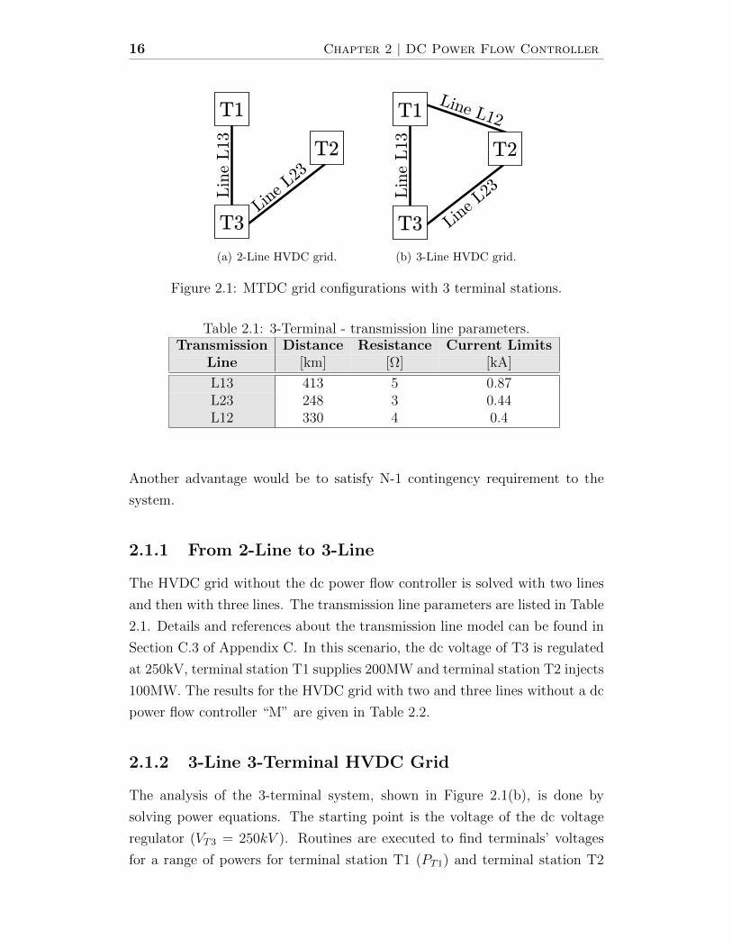
2.1 MTDC grid configurations with 3 terminal stations. . . . . . . . 16
2.2 Region of operation for the 3-terminal HVDC grid. . . . . . . . 18
2.3 3-terminal HVDC grid with a dc power flow controller M. . . . . 19
2.4 Example of the interaction with dc power flow controller. . . . . 19
2.5 Line current variations with respect to M with PT1=200MW
and PT2=100MW for the 3-terminal 3-line HVDC grid. . . . . . 21
2.6 Boundary analysis: line limits for the 3-terminal 3-line HVDC
grid. . . . . . . . . . . . . . . . . . . . . . . . . . . . . . . . . . 22
2.7 Transmission losses with respect to M for the 3-terminal 3-line
HVDC grid with PT2 = 100MW . . . . . . . . . . . . . . . . . . 23
2.8 MTDC grid configurations with 4 terminal stations. . . . . . . . 24
2.9 Region of operation for the 4-terminal HVDC grid with five
lines. The inside volume is without dc power flow controller M
and the expanded volume is with the controller. . . . . . . . . . 25
2.10 Region of operation with PT2=100MW. . . . . . . . . . . . . . . 26
2.11 Current variations with respect to M with PT1=100MW, PT2=100MW
and PT4=100MW for the 4-terminal 5-line HVDC grid . . . . . 27
3.1 DC Power Flow Controller: (a) shunt; and (b) series. . . . . . . 30
3.2 Thyristor power flow controller (TPFC) as an auxiliary con-
troller of VSC-HVDC station. . . . . . . . . . . . . . . . . . . . 32
3.3 Multiterminal HVDC formed from 3 VSC terminal stations. . . 33
3.4 Line currents-vs-VX and Node voltages-vs-VX for PT1 = 160MW
and PT2 = 80MW . . . . . . . . . . . . . . . . . . . . . . . . . . 34
xi
3.5 DC power flow controller: thyristor-based dual-converter. . . . . 36
3.6 Relationship between voltage and firing angle. . . . . . . . . . . 36
3.7 Thyristor power flow controller control diagram. . . . . . . . . . 37
3.8 Simulation Test 1 results: dc line currents and terminal voltages. 39
3.9 Simulation Test 1 results: thyristor power flow controller voltage. 39
3.10 Terminal station T1 ac-side arrangement. . . . . . . . . . . . . . 40
3.11 Simulation Test 2 results: dc line currents and terminal voltages. 41
3.12 Simulation Test 2 results: Thyristor power flow controller voltage. 41
3.13 Simulation Test 3 results: dc line currents and terminal voltages. 43
3.14 Simulation Test 3 results: thyristor power flow controller volt-
age, current and firing angle. . . . . . . . . . . . . . . . . . . . . 43
3.15 Simulation Test 4 results: dc line currents and terminal voltages. 45
3.16 Simulation Test 4 results: thyristor power flow controller voltage
and firing angle. . . . . . . . . . . . . . . . . . . . . . . . . . . . 45
3.17 Simulation Test 5 results: dc line currents and terminal voltages. 47
3.18 Simulation Test 5 results: thyristor power flow controller voltage. 47
3.19 VSC-Terminal station T1 connected to weak ac grid. . . . . . . 49
3.20 Simulation Test 6 results. . . . . . . . . . . . . . . . . . . . . . 49
4.1 7-Terminal HVDC grid configuration. . . . . . . . . . . . . . . . 52
4.2 Normal operation of the 7-terminal HVDC grid . . . . . . . . . 53
4.3 7-Terminal HVDC grid under different contingencies. . . . . . . 54
4.4 VSC Topology. . . . . . . . . . . . . . . . . . . . . . . . . . . . 56
4.5 7-Terminal HVDC grid simulation results: power injection/extraction
and terminal dc voltages. . . . . . . . . . . . . . . . . . . . . . . 57
4.6 7-Terminal HVDC grid simulation results: transmission line
currents and dc power flow controller. . . . . . . . . . . . . . . . 57
5.1 Single-stage Marx converter. . . . . . . . . . . . . . . . . . . . . 62
5.2 Operation states of the single-stage Marx converter. . . . . . . . 62
5.3 Voltage and current waveforms for the discharge from C1 in
series to COUT . The voltage waveforms neglect the output load
dynamic. . . . . . . . . . . . . . . . . . . . . . . . . . . . . . . . 63
5.4 Generalized Marx Converter with multiple stages (N) composed
of M capacitors per stage. . . . . . . . . . . . . . . . . . . . . . 63
5.5 The arrangements for the two sub-periods of equal duration tsw/2. 65
5.6 Ideal resonant waveforms for the currents and voltages. . . . . . 67
xii
5.7 Configuration when stage (n − 1) is charging (parallel connec-
tion) and stage n is discharging (series connection). . . . . . . . 70
5.8 Marx converter with 3-stage and 3 capacitors per stage (N=3,
M=3). . . . . . . . . . . . . . . . . . . . . . . . . . . . . . . . . 72
5.9 Simulation results in the two sub-periods S=1 and S=0. . . . . 74
5.10 Simulation results showing ripples on the output voltage and
output power. The ripples are associated with alternate switch-
ing states of the converter. . . . . . . . . . . . . . . . . . . . . . 75
5.11 Simulation results for inductor L1 current and output voltage
VOUT for a step-change in load. . . . . . . . . . . . . . . . . . . 76
5.12 Simulation results for inductor L1 current and output voltage
VOUT for a step change in the input voltage. . . . . . . . . . . . 77
6.1 Marx converter topology with N cascaded stages and M capac-
itors per stage. . . . . . . . . . . . . . . . . . . . . . . . . . . . 80
6.2 Inductor current waveform with dead-time period. . . . . . . . . 80
6.3 Output voltage VOUT waveform in the two state configurations:
the charging (S), followed by the discharge (S). The dead-time
occurs between (t1 to t2). . . . . . . . . . . . . . . . . . . . . . . 82
6.4 Output stage configuration. . . . . . . . . . . . . . . . . . . . . 83
6.5 Prototype configuration with N=2 and M=2. . . . . . . . . . . . 90
6.6 Simulation results for the prototype design. . . . . . . . . . . . . 92
7.1 Prototype converter. . . . . . . . . . . . . . . . . . . . . . . . . 95
7.2 Experimental setup for 5kW prototype converter with two stages
and two capacitors per stage. . . . . . . . . . . . . . . . . . . . 96
7.3 Details on experimental setup. . . . . . . . . . . . . . . . . . . . 97
7.4 1-Stage prototype configuration. . . . . . . . . . . . . . . . . . . 98
7.5 Experimental results for 1-stage prototype at 5kW. . . . . . . . 100
7.6 1-Stage prototype: gain and efficiency. . . . . . . . . . . . . . . 101
7.7 2-Stage prototype configuration. . . . . . . . . . . . . . . . . . . 101
7.8 Experimental results for 2-stage 5kW prototype. . . . . . . . . . 102
7.9 2-Stage prototype: gain and efficiency. . . . . . . . . . . . . . . 104
7.10 2-Stage prototype: load step change. . . . . . . . . . . . . . . . 105
7.11 2-Stage prototype: different switching frequencies. . . . . . . . . 105
7.12 Simulation results for accurate model of the prototype. . . . . . 106
xiii

8.1 Prototype configuration with N=2 and M=2. . . . . . . . . . . . 110
8.2 Converter state configurations with conducting switches displayed.111
8.3 Eigenvalues of ψ for operation in continuous conduction mode. . 114
8.4 Inductor current waveforms of converter operating in discontin-
uous conduction mode of operation. . . . . . . . . . . . . . . . . 115
8.5 State configurations for discontinuous conduction segment of
the converter in during logic states S and S. . . . . . . . . . . . 116
8.6 Detailed stage with components labelling. . . . . . . . . . . . . 118
8.7 Component volt-amp ratings for M=2, 4 and 16. . . . . . . . . . 125
8.8 Ratio MVA/Gain for configuration with M=2. . . . . . . . . . . 126
9.1 Offshore wind farm with Marx converter station to connect on
HVDC grid. . . . . . . . . . . . . . . . . . . . . . . . . . . . . . 130
9.2 Wind turbine characteristic curves for fix pitch angle (β = 0). . 131
9.3 Wind turbine converter. . . . . . . . . . . . . . . . . . . . . . . 132
9.4 Wind turbine control diagram. . . . . . . . . . . . . . . . . . . . 133
9.5 Wind turbine converter characteristics when operating at MPPT.134
9.6 Wind turbine converter boundary for continuous conduction
mode (CCM) and discontinuous conduction mode (DCM). . . . 135
9.7 Marx offshore station. . . . . . . . . . . . . . . . . . . . . . . . 137
9.8 Control diagram of the step-up converter included in the Marx
offshore station. . . . . . . . . . . . . . . . . . . . . . . . . . . . 139
9.9 Simulation results for operation of the system from high wind
to low wind condition. . . . . . . . . . . . . . . . . . . . . . . . 140
9.10 Simulation results of the Marx converter inductor waveforms at
low wind condition. . . . . . . . . . . . . . . . . . . . . . . . . . 141
10.1 Complete multiterminal HVDC system with dc power flow con-
troller and Marx offshore station. . . . . . . . . . . . . . . . . . 145
10.2 Simulation results of the offshore wind farm. . . . . . . . . . . . 147
10.3 Simulation results for power and voltage at terminal stations. . . 147
10.4 Simulation results of the transmission line currents. . . . . . . . 149
10.5 Simulation results of dc power flow controller response. . . . . . 149
10.6 Simulation results of the Marx converter operating at high wind. 150
C.1 VSC model. . . . . . . . . . . . . . . . . . . . . . . . . . . . . . 168
C.2 VSC dq-controller. . . . . . . . . . . . . . . . . . . . . . . . . . 168
xiv

C.3 VSC d-axis controller options. . . . . . . . . . . . . . . . . . . . 169
C.4 VSC and thyristor power flow controller configuration. . . . . . 169
C.5 Thyristor power flow controller: voltage controller. . . . . . . . . 170
C.6 Thyristor power flow controller: V refX controller options. . . . . . 170
C.7 Implementation overview on Opal-RT system. . . . . . . . . . . 172
D.1 Prototype nameplate. . . . . . . . . . . . . . . . . . . . . . . . . 175
D.2 Gate driver interface board. . . . . . . . . . . . . . . . . . . . . 182
D.3 Inductors used for experimental work. . . . . . . . . . . . . . . . 182
D.4 Pictures of laboratory setup for prototype experiment. . . . . . 183
D.5 Detailed simulation model implemented in PSCAD-EMTDC
software package. . . . . . . . . . . . . . . . . . . . . . . . . . . 184
xv

xvi

List of Tables
1.1 Control references of HVDC terminal station . . . . . . . . . . . 6
2.1 3-Terminal - transmission line parameters. . . . . . . . . . . . . 16
2.2 3-Terminal - scenarios. . . . . . . . . . . . . . . . . . . . . . . . 17
2.3 4-Terminals - transmission line parameters. . . . . . . . . . . . . 24
2.4 4-Terminals - scenarios. . . . . . . . . . . . . . . . . . . . . . . . 25
3.1 System parameters. . . . . . . . . . . . . . . . . . . . . . . . . . 33
3.2 Mode of operation of converters. . . . . . . . . . . . . . . . . . . 35
3.3 Simulation Test 1. . . . . . . . . . . . . . . . . . . . . . . . . . . 38
4.1 VSC control references . . . . . . . . . . . . . . . . . . . . . . . 52
4.2 Transmission line parameters . . . . . . . . . . . . . . . . . . . 53
4.3 N-1 contingency scenarios . . . . . . . . . . . . . . . . . . . . . 55
5.1 Simulation parameters . . . . . . . . . . . . . . . . . . . . . . . 72
5.2 Design values and simulation results . . . . . . . . . . . . . . . . 75
6.1 Design parameters. . . . . . . . . . . . . . . . . . . . . . . . . . 91
6.2 Capacitor voltages and inductor currents. . . . . . . . . . . . . . 93
7.1 1-Stage prototype: parameters. . . . . . . . . . . . . . . . . . . 99
7.2 1-Stage prototype: steady-state measurements. . . . . . . . . . . 99
7.3 2-Stage prototype: parameters. . . . . . . . . . . . . . . . . . . 103
7.4 2-Stage prototype: steady-state measurements. . . . . . . . . . . 103
8.1 Eigenvalues of ψ and ψ. . . . . . . . . . . . . . . . . . . . . . . 114
8.2 IGBT ratings. . . . . . . . . . . . . . . . . . . . . . . . . . . . . 118
8.3 Diode ratings. . . . . . . . . . . . . . . . . . . . . . . . . . . . . 120
8.4 Capacitor ratings. . . . . . . . . . . . . . . . . . . . . . . . . . . 122
8.5 Inductor ratings. . . . . . . . . . . . . . . . . . . . . . . . . . . 123
xvii

8.6 Volt-amp rating comparison for converter gain of 16. . . . . . . 125
9.1 Wind turbine and generator parameters . . . . . . . . . . . . . . 131
9.2 Wind turbine converter parameters . . . . . . . . . . . . . . . . 136
9.3 50MW wind turbine . . . . . . . . . . . . . . . . . . . . . . . . 136
9.4 Marx offshore station parameters . . . . . . . . . . . . . . . . . 138
9.5 Transmission line parameters . . . . . . . . . . . . . . . . . . . 139
9.6 Simulation results at low wind condition . . . . . . . . . . . . . 141
10.1 Simulation results of the power at terminal stations. . . . . . . . 146
10.2 Simulation results for transmission line currents and powers. . . 149
10.3 Simulation results of the Marx converter. . . . . . . . . . . . . . 151
C.1 HVDC transmission line parameters . . . . . . . . . . . . . . . . 170
C.2 Simulation parameters of Chapter 3. . . . . . . . . . . . . . . . 171
C.3 Simulation parameters of Chapter 4. . . . . . . . . . . . . . . . 173
C.4 Simulation parameters of Chapter 4. . . . . . . . . . . . . . . . 174
D.1 Simulation model parameters. . . . . . . . . . . . . . . . . . . . 184
xviii

List of Acronyms
AC or ac Alternating Current
DC or dc Direct Current
FACTS Flexible AC Transmission System
GTO Gate Turn-Off Thyristor
HVDC High Voltage Direct Current
IGBT Insulated Gate Bipolar Transistor
IGCT Insulated Gate-Commutated Thyristor
MMC Modular Multilevel Converter
MPPT Maximum Peak Power Tracking
MTDC Multiterminal HVDC
PMSG Permanent Magnet Synchronous Generator
THD Total Harmonic Distortion
VSC Voltage Source Converter
xix

xx

Chapter 1
Introduction
1.1 Background
High Voltage Direct Current (HVDC) technology has been applied mainly in
two aspects of power engineering: bulk power transmission over long distance
and interconnection between two ac networks of different frequencies or same
frequency but different phase angles. The development of self-commutating
power electronics switches suitable for high power and high voltage has ex-
tended the range of application of HVDC. For example, the recent submarine
link in the San Francisco region is using HVDC with self-commutating technol-
ogy [1,2]. Similar technology is used for offshore wind farms like the BorWin1
project linking the BARD Offshore 1 wind farm to Germany [3].
Multiterminal HVDC (MTDC) has been of interest since the earliest days of
HVDC transmission [4,5]. HVDC then was based on current source converters
of line-commutated thyristors. As current source converters are not suitable for
parallel connection, MTDC based on them came to a halt. With the arrival of
voltage source converters (VSC) based on self-commutating switches (GTOs,
IGBTs, IGCTs, etc), HVDC has a revival, for example, under the tradename
like HVDC Lightr (ABB) or HVDC PLUS (Siemens). As VSCs are suitable
for parallel connection across the dc terminals, VSCs are considered as the
technology for providing a HVDC grid. MTDC is a serious contender for
future transmission projects especially the ones related to renewable energy.
Supergrids have proposed MTDC to bring offshore wind farm power on-
shore, to transmit solar energy produced in north Africa to Europe and to
create power transfer corridors [6–9]. The rationale for considering the self-
commutating converter family for MTDC is that their dc sides are ideal-current
1

2 Chapter 1 |
Wind farm:80 units
AC
Offshoreplatform:ac collector
AC/DC
Offshoreplatform:
rectifier station
Onshoreinverterstation
400MW
1km 125km submarine75km underground
DC/AC
33kVac
155kVac±150kVdc 380kVac
(a) BARD Offshore 1 wind farm project.
Wind farm
DC/DC
Offshore platform:dc/dc transformer
Onshoreinverter station
DC/AC
mediumdc voltage ac
grid
highdc voltage
(b) Offshore wind farm with dc collector bus.
Figure 1.1: Examples of offshore wind farm arrangements.
sources and, therefore, they can be connected in parallel naturally.
There are still many challenges that need to be addressed in order to put
in operation such MTDC. Among them, the limitation regarding the power
flow control is major obstacle as discussed in [10]. As opposed to ac network
where both the voltage magnitude and the angle can be controlled, only the
voltage magnitude can be regulated in a MTDC.
A suitable MTDC system should offer enough flexibility to control the
power flow without imposing limitations on transmission lines connected to a
terminal station. To address this issue, the addition of an auxiliary dc voltage
controller is proposed in this thesis. By doing so, the MTDC power flow
controllability is improved.
The application of MTDC for offshore wind farm is also studied. The
aggregation and transmission of wind power from offshore to the mainland
remains a technical challenge. Actual configuration includes the construction
of offshore platforms to install equipment required for transmitting power on-
shore. Figure 1.1(a) shows the example of the BARD Offshore 1 wind farm
project where two platforms were required [3, 11, 12]. It would be an advan-
tage to avoid such arrangement by having a configuration that would allow
Introduction | 3
transmission with the need of only one offshore platform. The ac transformers
on the offshore platform are the largest single equipment installed [13] and it
requires expensive structural design to support its heavy weight.
By eliminating the ac collector offshore platform, the structural require-
ment for heavy ac transformers can be avoided but the challenge is to bridge
the two voltages without ac transformers but rather with dc-dc transformer
as shown in Figure 1.1(b). A dc collector bus would then be required to
gather the wind power to the dc-dc transformer platform. In this research, an
offshore wind farm configuration is developed to interconnect wind turbines
and to transmit power onshore. A dc-dc converter topology suitable for this
application is presented in this thesis.
1.2 Scope
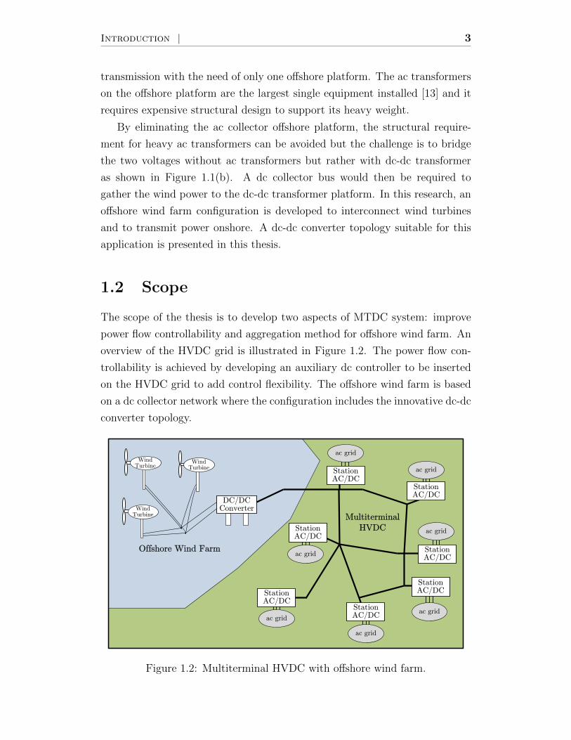
The scope of the thesis is to develop two aspects of MTDC system: improve
power flow controllability and aggregation method for offshore wind farm. An
overview of the HVDC grid is illustrated in Figure 1.2. The power flow con-
trollability is achieved by developing an auxiliary dc controller to be inserted
on the HVDC grid to add control flexibility. The offshore wind farm is based
on a dc collector network where the configuration includes the innovative dc-dc
converter topology.
ac grid
Offshore Wind Farm
StationAC/DC
ac grid
ac grid
ac grid
ac grid
ac grid
MultiterminalHVDC
ac grid
WindTurbine
WindTurbine
WindTurbine
DC/DCConverter
StationAC/DC
StationAC/DC
StationAC/DC
StationAC/DC
StationAC/DC
StationAC/DC
Figure 1.2: Multiterminal HVDC with offshore wind farm.
4 Chapter 1 |
1.3 Literature Review
1.3.1 HVDC Grid
Three main converter topologies are currently used for HVDC system. The
thyristor-based converter, also called conventional HVDC, is used for bulk
power transmission system [14]. It is a mature technology that has proven its
robustness through the years. Originally around ±400kV, the voltage rating
can go up to ±800kV in Ultra High Voltage Direct Current system (UHVDC).
However, this converter topology requires a strong ac grid voltage since it is a
line-commutated converter and it consumes reactive power.
Initially constructed for low and medium voltage, the VSC based on IGBTs
has entered the high voltage range. It has the advantage of having better
control of its reactive power consumption and it can be connected to a weak
ac system [15]. The typical voltage range is around ±250kV but it can go
higher.
The third topology is a configuration based on multilevel converter. The
modular multilevel converter (MMC) is based on half-bridge submodules con-
nected in series [16,17]. The modularity of the concept makes it a very attrac-
tive solution to the industry. The operation advantages are similar as for the
VSC since it also uses IGBTs as power electronics switches.
In developing HVDC grid, VSC and MMC are both expected to be involved.
In this thesis, MTDC is based on VSC terminal stations but the conclusions
obtained can be extended to MMC-based HVDC grid.
Among the challenges of developing HVDC grid, the behaviour of the con-
verter under faulty conditions is of particular interest. As opposed to ac, dc
current does not pass by zero periodically which makes it difficult to break the
dc fault current. This issue is out of the scope of the thesis but it is worth
mentioning that many researchers are addressing the situation and they have
proposed various analysis and solutions [18–23].
The limitation of only controlling the dc voltage magnitude has an impact
on the power flow control of the HVDC grid [6,10]. In MTDC with thyristor-
based converter, power flow control using telecommunication and central ref-
erence balancer has been suggested in [24]. However, it is desirable to have the
controls independent of telecommunication link especially in the perspective
of a large MTDC. Recent proposals have suggested the use of master/slave
control [25, 26] and voltage droop control [27–31]. In both approaches, the
Introduction | 5
control strategy varies but the MTDC remains with the same limited number
of controls.
Another approach to redistribute the power transmitted on HVDC lines
is to insert a device for additional voltage control into the HVDC grid. The
installation of an auxiliary dc voltage controller at one end of the line can
influence the power flow if it can vary the voltage on that line. The thesis
presents a solution for this power flow control problem through an auxiliary
dc voltage controller inserted in a dc transmission line.
The controls of ac system and dc grid are different. AC bus has two degrees
of freedom: ac voltage magnitude and phase angle. They enable PQ control
and there are four different types of buses used in power flow analysis. More
precisely, they are voltage-controlled (PV), load (PQ), device (special type
like HVDC converters) and slack (swing) buses [32]. Each bus has parameters
which define voltage magnitude, voltage angle, real power and/or reactive
power. In contrast, only the dc voltage can be controlled in MTDC systems.
So, three different categories of terminal stations can be defined for HVDC
systems:
1. Voltage regulator acts as the dc bus reference. It is also called the “slack
bus” because it controls the ac active power, Pslack, so that the algebraic
sum of power in the HVDC grid is zero. The Q control on the ac side
supports the ac voltage.
2. Controlled power injection has a specific power contribution into the
HVDC grid. It can be either positive (generation) or negative (load). It
is also called complex power dispatcher because the converter regulates
both the real and reactive power on the ac side (PQ control).
3. AC bus reference regulates the ac side voltage and frequency. Commonly
used for wind farm where it serves the equivalent of an infinite ac bus.
Table 1.1 summarizes the categories and their control references. In this thesis,
only the first two types of terminal stations are used.
Connecting offshore wind farms to a HVDC grid poses interesting chal-
lenges [33,34]. Conventional arrangement, as shown in Figure 1.1(a), involves
many power conversion steps from ac to dc and vice-versa. The wind turbine
outputs ac at varying frequency which is then converted to ac at fixed fre-
quency via an ac-dc-ac converter. The power from the wind turbines of the

6 Chapter 1 |
Table 1.1: Control references of HVDC terminal stationAC Side DC Side
Voltage Regulator Pslack Qref V refdc
Controlled AC P ref Qref Vdc from dcPower Injection circuit analysisAC bus reference V ref f ref Vdc from dc
P and Q vary circuit analysis
wind farms is collected in ac and then it is rectified to dc for HVDC trans-
mission. By avoiding the intermediate ac collector network, the wind turbines
are interconnected using dc link [35]. The elimination of the wind turbine ac
transformer can improve the overall efficiency of the unit by up to 1.4% [36].
The wind farm configuration used for this research is parallel connection of
wind turbine units [37–39]. The units are connected to a common dc link and
there is a converter station with a dc-dc converter to bridge the dc collector
network to the HVDC grid for transmission purposes.
1.3.2 DC-DC Converter
High voltage, high dc power supplies are used in scientific, medical and military
community for applications in systems related to X-ray, radar, travelling wave
tubes (TWT) and TEA lasers. The power levels range from 120mW to 150kW
with voltages from few volts to 500kV for airborne, satellite and space station
environment where iron core transformers are to be avoided.
The technologies which can step-up to very high voltages without trans-
formers make use of Ldi/dt boost voltages [40–42], LC resonance [41,42], LCC
resonance [40] or switched-capacitor converter [43].
The topologies using Ldi/dt take advantage of the rapid change of current
in an inductor to create a large voltage. The stepped-up voltage is then cap-
tured at an output stage. The example of the conventional step-up (boost)
converter is shown in Figure 1.3(a). Topologies using LC and LCC resonances
create an oscillatory environment to amplify the voltage. Figure 1.3(b) shows
a parallel tank circuit for LC and Figure 1.3(c) shows an arrangement for LCC
resonance. The topologies using switched-capacitor creates higher voltage by
connecting capacitors in series. An example is shown in Figure 1.3(d).
This thesis revisits the Marx generator concept which was invented in Ger-
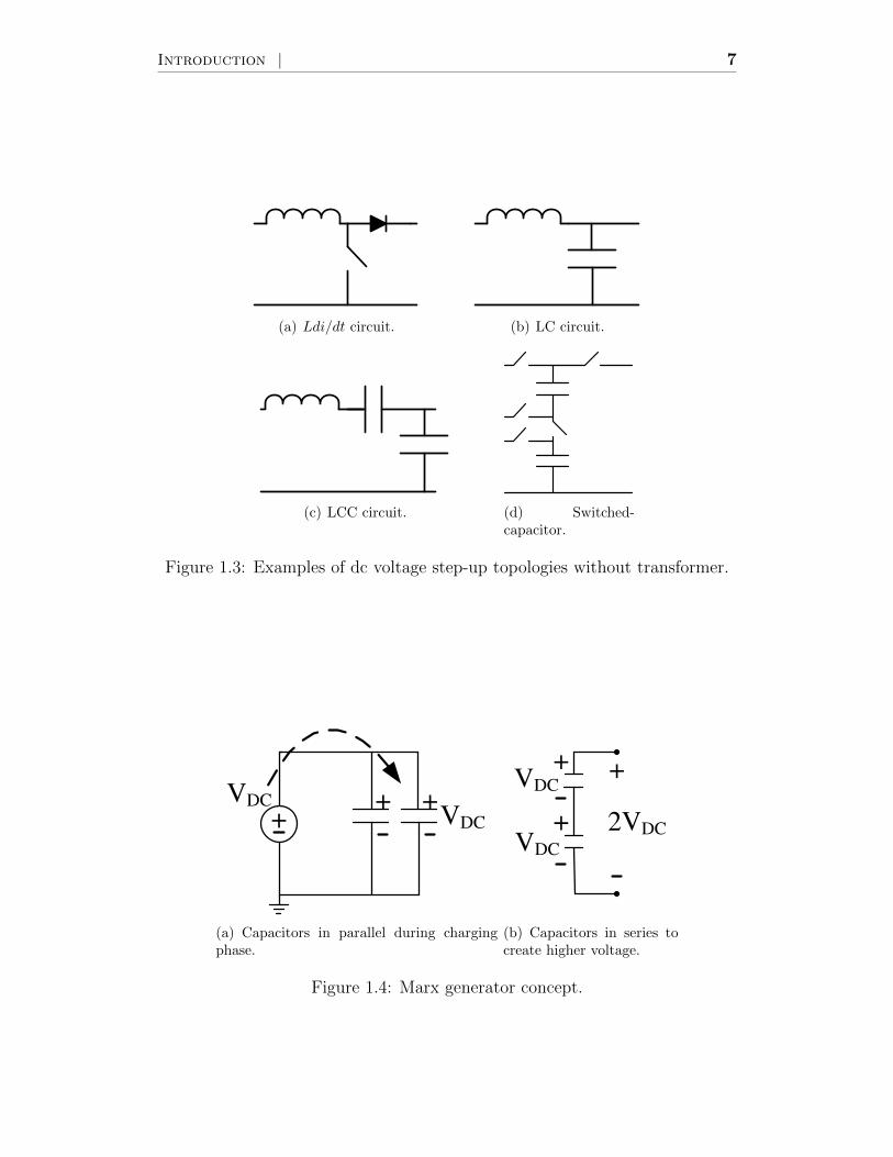
Introduction | 7
(a) Ldi/dt circuit. (b) LC circuit.
(c) LCC circuit. (d) Switched-capacitor.
Figure 1.3: Examples of dc voltage step-up topologies without transformer.
+
VDC + +VDC
(a) Capacitors in parallel during chargingphase.
++
+VDC
VDC
2VDC
(b) Capacitors in series tocreate higher voltage.
Figure 1.4: Marx generator concept.

8 Chapter 1 |
many by Erwin Marx around 1923 [44,45]. The concept of the Marx generator
is shown in Figure 1.4 for a dc amplification of 2. It consists of charging capac-
itors in parallel, shown in Figure 1.4(a), followed by a reconnection in series
for creating higher output voltage, shown in Figure 1.4(b). The classical Marx
generator uses spark gaps to connect capacitors in series and to create a single
high voltage pulse. Adaptations of the original topology have been made for
insulation testing of high voltage equipment [46] and X-ray generation [47].
Nowadays with solid-state switches, modern topologies based on the same
principle of connecting capacitors in series and in parallel have been presented
in [48–61]. The application varies from research laboratory [56, 57] to photo-
voltaic [58] and even inverter converter [53]. However, most of the topologies
presented are pulse generation type of converter and they are not suitable for
continuous high power application. The research of this thesis is oriented to-
ward applications where heavy ac transformer should be avoid but dc voltage
step-up is still required to bridge the low voltage of offshore wind turbine to
the high voltage of HVDC grid.
The objective of the thesis is to develop a high power Marx converter
suitable for continuous current operation. In order to reach very high dc
voltage gain at economical cost, the concept of cascading stages is incorporated
into the research [62–65]. By doing so, an overall dc gain ofMN can be achieved
by using N stages of Marx modules, each having a gain of M. The research in
the thesis resides in the new dc-dc converter topology developed.
1.4 Research Objectives
The objective of the thesis is to improve power controllability of the HVDC
grid. Unlike ac systems which have two degrees of controllability (P and Q),
the HVDC grid depends on the value of the dc voltage at the terminals [10].
The thesis proposes the dc power flow controller to address this deficiency in
Chapters 2 to 4.
The next issue relates to offshore wind farm which transmits dc power.
Because the weight of iron transformer add to civil engineering cost, the thesis
investigates the possibility of dc-dc conversion with dc voltage amplification
without ac transformer. The solution proposed is the Marx dc-dc converter of
Chapters 5 to 9.
Introduction | 9
1.5 Thesis Contributions
The items listed below are original contributions in the area of power engi-
neering, HVDC systems and dc-dc converter.
1.5.1 DC Power Flow Controller
• The DC Power Flow Controller, as an auxiliary controller of a VSC
station, based on thyristor-based dual-converter. The DC Power Flow
Controller is inserted in a dc transmission line to increase the control-
lability of a dc grid based on multiterminal HVDC. (Chapters 3 and
4)
• Apart from the realization of the controller, the research has evaluated
that the controller does increase the feasible region of operation of the
dc grid thus justifying its presence. (Chapter 2)
1.5.2 Marx DC-DC Converter
• The innovative dc-dc converter, which has been adapted from the well
known Marx generator to serve as a continuous high voltage, high power
dc-dc converter. Besides simulation, experimental prototypes have been
constructed and tested for proof of concept. (Chapters 5-7)
• Innovation, which consists of electric charge transfers from the input end
to the output end using L-C resonance with a diode to the inductor to
ensure continuous, unidirectional power transfer. (Chapters 5 and 6)
• Innovation, which consists of design equations for determining the ca-
pacitor size for dc voltage gain M. (Chapter 6)
• Innovation, which consists of applying cascading stages to the Marx dc-dc
converter. As the dc voltage increases in each stage, it has a correspond-
ing current decrease whereby the VA rating is constant at each stage.
(Chapters 5 and 6)
• An innovative method of asymptotic stability analysis based on solving
linear equations x = Ax + Bu in each sub-period of IGBT switching
and integrating the output states at the end of the kth sub-period as
the initial state of the (k+1)th sub-period. Stability is assured when the
10 Chapter 1 |
eigenvalues are lying within the unit circle in the complex plane. (Section
8.1 of Chapter 8)
• A method of cost evaluation for the choice of N (the number of cascading
stages) and M (the dc voltage gain of each stage) to achieve an overall
dc voltage gain of MN . The method depends on deriving equations
for components based on the voltage and current ratings at each stage.
(Section 8.2 of Chapter 8)
1.6 Thesis Overview
The thesis is organized such that the dc power flow controller is explained in
Part I (Chapters 2 to 4) and the dc-dc converter topology is described in Part II
(Chapters 5 to 9). Finally, in Part III (Chapter 10), the dc power flow controller
and the dc-dc converter topology are integrated to form a complete MTDC
system with offshore wind farm integration and power flow controllability.
1.6.1 Part I: DC Power Flow Controller
Chapter 2 presents the concept and the benefits of the dc power flow controller.
The operation of the controller within a MTDC is described and it is shown
for 3-terminal and 4-terminal HVDC grids. Chapter 3 details the hardware
realization of the dc power flow controller. Control strategy is presented and
implemented on a 3-terminal HVDC system. The system is fully modeled
with VSC stations and the dc power flow controller. Chapter 4 studies a
larger MTDC composed of 7 terminal stations. Various scenarios are discussed
including transmission line contingency.
1.6.2 Part II: Marx DC-DC Converter
Chapter 5 describes the basic configuration of the Marx dc-dc converter. Mod-
els for single-stage and cascade configuration are analyzed. Chapter 6 intro-
duces design guidelines. The analysis includes considerations such as losses
and dead-time requirements. Chapter 7 shows the 5kW prototype constructed.
Laboratory test results are obtained to demonstrate the operation of the con-
verter. Chapter 8 analyzes the stability of the converter through piecewise

Introduction | 11
linear approach. In addition, parameters ratings are evaluated for the semicon-
ductor switches and passive components (inductors and capacitors). Chapter
9 describes a 200MW offshore wind farm connected to a VSC station via a
Marx offshore station.
1.6.3 Part III: Complete Multiterminal HVDC System
Chapter 10 shows a complete system composed of a 7-terminal HVDC grid
with a dc power flow controller and a 200MW offshore wind farm. The chapter
integrates the two research topics addressed in Parts I and II of the thesis.
Finally, the conclusion is in Chapter 11. It provides a summary of the
thesis, conclusions from the research of this thesis, the list of original contri-
butions and it discusses of future work. The associated publications related to
this work are listed in Appendix A.

12 Chapter 1 |
Part I
DC Power Flow Controller
13

14
Chapter 2
DC Power Flow Controller:
Concept and Benefits
In this chapter, the concept of the dc power flow controller is explained. A
simple 3-terminal system is described to give a good picture of the situation.
The 3-terminal system has initially two transmission lines and it is upgraded to
three lines. The 3-line 3-terminal system is introduced with the dc power flow
controller and the benefits are evaluated using the region of operation. Then,
a 4-terminal system is explored. The objective of the chapter is to evaluate
the benefits of a dc power flow controller inserted on a transmission line using
two case studies: a 3-terminal grid with three lines and a 4-terminal grid with
five lines.
2.1 System Description
In the 3-terminal system shown in Figure 2.1(a), terminal stations T1 and T2
are fixed-power terminal stations and terminal station T3 is the voltage regu-
lator. The scenario can be an interconnection between two countries (terminal
stations T1 and T2) via submarine dc cables (link L13) and a wind farm (T2)
is connected onshore to T3 by link L23. In the perspective of developing a
HVDC grid, a third line can be installed between terminal stations T1 and
T2 as shown in Figure 2.1(b). In the proposed scenario, the justification can
be to maximize the use of the already built link L23 when low wind power is
produced. For the benefit of the argument, it is assumed that the addition of
the line L12 would be less costly than a new line from T1 to T3. By doing
so, it offers the ability to transmit power from T1 to T3 via the link L12-L23.
15
16 Chapter 2 | DC Power Flow Controller
T2
T1
T3LineL13
LineL23
(a) 2-Line HVDC grid.
T3
LineL13
T1
T2
Line L12
LineL23
(b) 3-Line HVDC grid.
Figure 2.1: MTDC grid configurations with 3 terminal stations.
Table 2.1: 3-Terminal - transmission line parameters.Transmission Distance Resistance Current Limits
Line [km] [Ω] [kA]
L13 413 5 0.87L23 248 3 0.44L12 330 4 0.4
Another advantage would be to satisfy N-1 contingency requirement to the
system.
2.1.1 From 2-Line to 3-Line
The HVDC grid without the dc power flow controller is solved with two lines
and then with three lines. The transmission line parameters are listed in Table
2.1. Details and references about the transmission line model can be found in
Section C.3 of Appendix C. In this scenario, the dc voltage of T3 is regulated
at 250kV, terminal station T1 supplies 200MW and terminal station T2 injects
100MW. The results for the HVDC grid with two and three lines without a dc
power flow controller “M” are given in Table 2.2.
2.1.2 3-Line 3-Terminal HVDC Grid
The analysis of the 3-terminal system, shown in Figure 2.1(b), is done by
solving power equations. The starting point is the voltage of the dc voltage
regulator (VT3 = 250kV ). Routines are executed to find terminals’ voltages
for a range of powers for terminal station T1 (PT1) and terminal station T2

Concept and Benefits | 17
Table 2.2: 3-Terminal - scenarios.2-Line 3-Line 3-Line 3-Line
no M with M with MFig. 2.1(a) Fig. 2.1(b) Fig. 2.4(a) Fig. 2.4(b)
PT1 [MW] 200 200 200 ↑ 220PT2 [MW] 100 100 100 ↓ 80VT3 [kV] 250 250 250 250M - - 0.989 ↑ 0.991
VT1 [kV] 253.9 252.8 254.0 253.9VT2 [kV] 251.2 251.9 251.2 251.2IL12 [kA] 0.788 0.561 0.792 0.776IL23 [kA] 0.398 0.627 0.394 0.410IL12 [kA] - 0.230 -0.004 0.091
(PT2). To determine if the operating point is valid, line currents are calculated
and it is determined if currents are exceeding the limits listed in Table 2.1.
The calculation algorithm and details are given in Appendix B. In a HVDC
grid, the currents are calculated using voltages and line resistances only. The
equations of the currents are:
IL13 =VT1 − VT3
RL13
(2.1)
where the current limit is 0.87kA,
IL23 =VT2 − VT3
RL23
(2.2)
where the current limit is 0.44kA,
IL12 =VT1 − VT2
RL12
(2.3)
where the current limit is 0.4kA. Using those equations, the power equations
for terminal stations T1 and T2 are given as:
PT1 = V 2T1
[1
RL13
+1
RL12
]+ VT1
[−VT3
RL13
+VT2
RL12
](2.4)
PT2 = V 2T2
[1
RL23
+1
RL12
]+ VT2
[−VT3
RL23
+VT1
RL12
](2.5)

18 Chapter 2 | DC Power Flow Controller
−300 −200 −100 0 100 200 300−250
−200
−150
−100
−50
0
50
100
150
200
250
PT1
− [MW]
P T2 −
[MW
]
2 Lines3 Lines without M3 Lines with M
Figure 2.2: Region of operation for the 3-terminal HVDC grid.
The region in gray of Figure 2.2 is the operable region of the 3-line system. The
figure also depicts in black the region of operation for the 3-terminal system
with only two lines.
2.2 DC Power Flow Controller
2.2.1 Description
The dc power flow controller is conceived as a mean to change the voltage at the
dc terminals of a VSC station by a ratio M. The dc power flow controller can
be modeled either as an ideal converter (Pin = Pout) or as some kind of power
injection device. In this chapter, the dc power flow controller is modeled as an
ideal converter whose input is VSC terminal voltage VV SC and whose output is
dc line voltage Vline. The practical implementation is described in Chapter 3.
The ratio M is the output-to-input voltage ratio of the ideal converter as given
in Equation (2.6).
M =VlineVV SC
(2.6)
Among many requirements, the dc power flow controller has to be eco-
nomical in order to be viable. It can be rated for only a fraction of the
terminal converter ratings because line currents are very sensitive to voltage
Concept and Benefits | 19
IL13
IL23
IL12M
RL13
RL23
RL12
PT1
T1
PT2
T2
T3
VT3
Figure 2.3: 3-terminal HVDC grid with a dc power flow controller M.
0.792kA
PT1=200MW
VT3=250kV
0.394kA
-0.004kA
0.989MT1
T2
T3
PT2=100MW
(a) With M=0.989, the operation issimilar to the 2-line configuration.
0.776kA
PT1= 220MW
VT3=250kV
0.410kA
0.091kA
0.991MT1
T2
T3
PT2= 80MW
(b) Variation in power injection.
Figure 2.4: Example of the interaction with dc power flow controller.
variations due to the low line resistances. Therefore, a variation of voltage of
only 5%(±2.5%) is considered in this project.
2.2.2 Benefits
The 3-line system shown in Figure 2.1(b) is upgraded with a dc power flow
controller “M” as illustrated in Figure 2.3. The ratio M is adjusted to force
the HVDC grid to operate back with the same current values as with 2 lines
(Figure 2.1(a)). A ratio of 0.989 makes the current in the link L12 almost zero,
which reproduces the initial conditions. This situation is illustrated in Figure
2.4(a).
In the event that the wind farm (terminal station T2) production reduces
to 80MW instead of 100MW, the terminal station T1 is able to increase its
20 Chapter 2 | DC Power Flow Controller
power injection by 20MW to compensate the reduction. However, it is required
that the 20MW of extra power is transmitted via the L12-L23 link and not
L13 because line L12 is already at its nominal capacity. Then, the dc power
flow controller is adjusted to 0.991 which forces the 20MW to flow via link
L12-L23 as shown in Figure 2.4(b). More details about currents, voltages and
powers for both scenarios are given in Table 2.2.
This simple example describes the operation and benefits of the inserted
dc power flow controller on the HVDC grid. The extra contribution of 20MW
by terminal station T1 might appear to be unrealistic for an already installed
converter with established power ratings. However, in the vision of a future
HVDC grid, it is most likely that a terminal station T1, for example, will
branch out to many converters and several dc power flow controllers may be
installed. In that case, the requirement of additional power controllability
would be served.
2.2.3 Region of Operation
As expected, the restricted region enlarges with the addition of the dc power
flow controller. The dc power flow controller is inserted in the HVDC grid on
line L12 between terminal stations T1 and T2 as in Figure 2.3. The equation
of the current in line L12 becomes,
IL12 =MVT1 − VT2
RL12
(2.7)
where M is the output-to-input ratio of the dc power flow controller. The
system is solved by updating Equations (2.4) and (2.5) to:
PT1 = V 2T1
[1
RL13
+M2
RL12
]+ VT1
[−VT3
RL13
+MVT2
RL12
](2.8)
PT2 = V 2T2
[1
RL23
+1
RL12
]+ VT2
[−VT3
RL23
+MVT1
RL12
](2.9)
The boundary of the region of operation is the dotted line in Figure 2.2.
This illustrates that the insertion of the dc power flow controller indeed en-
larges the area offering more options to transmit power. The increase is sig-
nificant compared to the system without M; it increases by 112% for the four
quadrants.
Concept and Benefits | 21
0.97 0.98 0.99 1 1.01 1.02 1.03−0.5
0
0.5
1
1.5
M
Cur
rent
− [k
A]
IL13
IL23
IL12
Figure 2.5: Line current variations with respect to M with PT1=200MW andPT2=100MW for the 3-terminal 3-line HVDC grid.
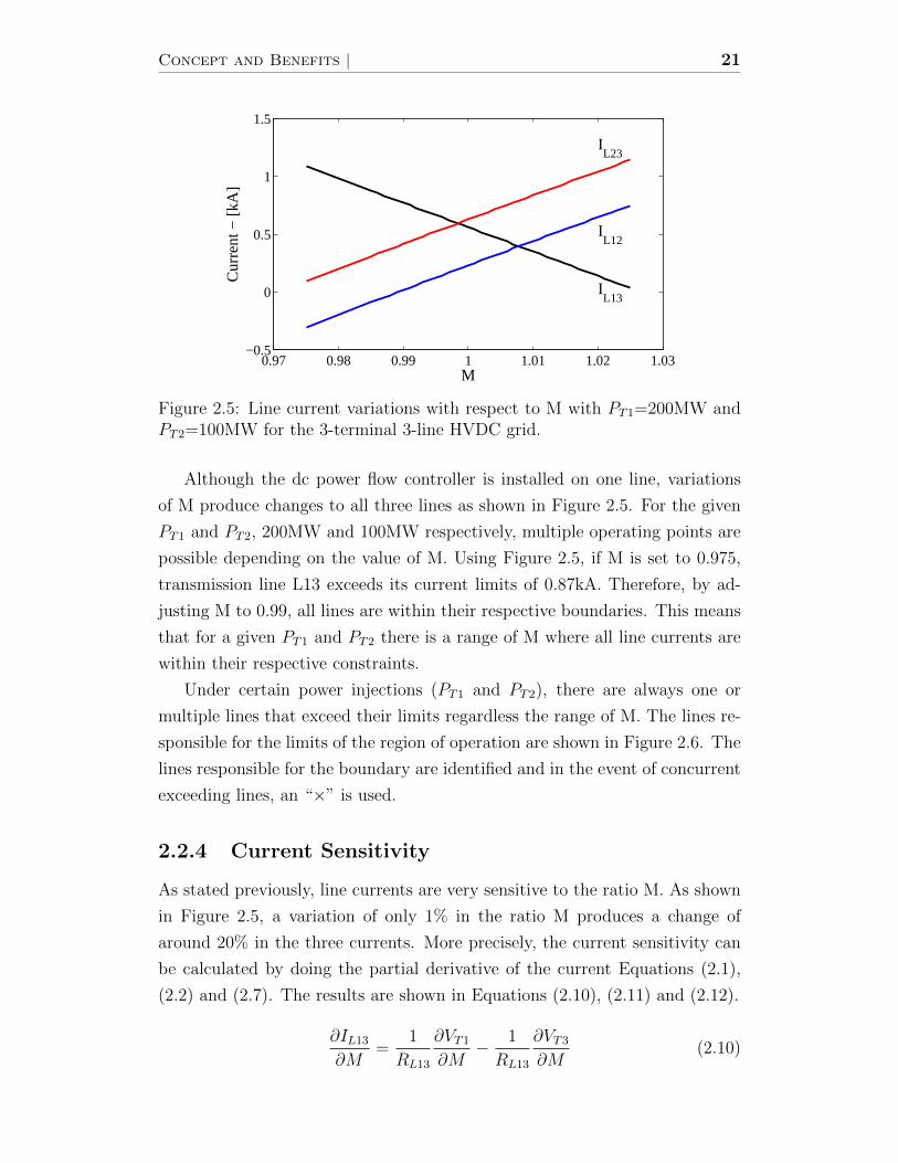
Although the dc power flow controller is installed on one line, variations
of M produce changes to all three lines as shown in Figure 2.5. For the given
PT1 and PT2, 200MW and 100MW respectively, multiple operating points are
possible depending on the value of M. Using Figure 2.5, if M is set to 0.975,
transmission line L13 exceeds its current limits of 0.87kA. Therefore, by ad-
justing M to 0.99, all lines are within their respective boundaries. This means
that for a given PT1 and PT2 there is a range of M where all line currents are
within their respective constraints.
Under certain power injections (PT1 and PT2), there are always one or
multiple lines that exceed their limits regardless the range of M. The lines re-
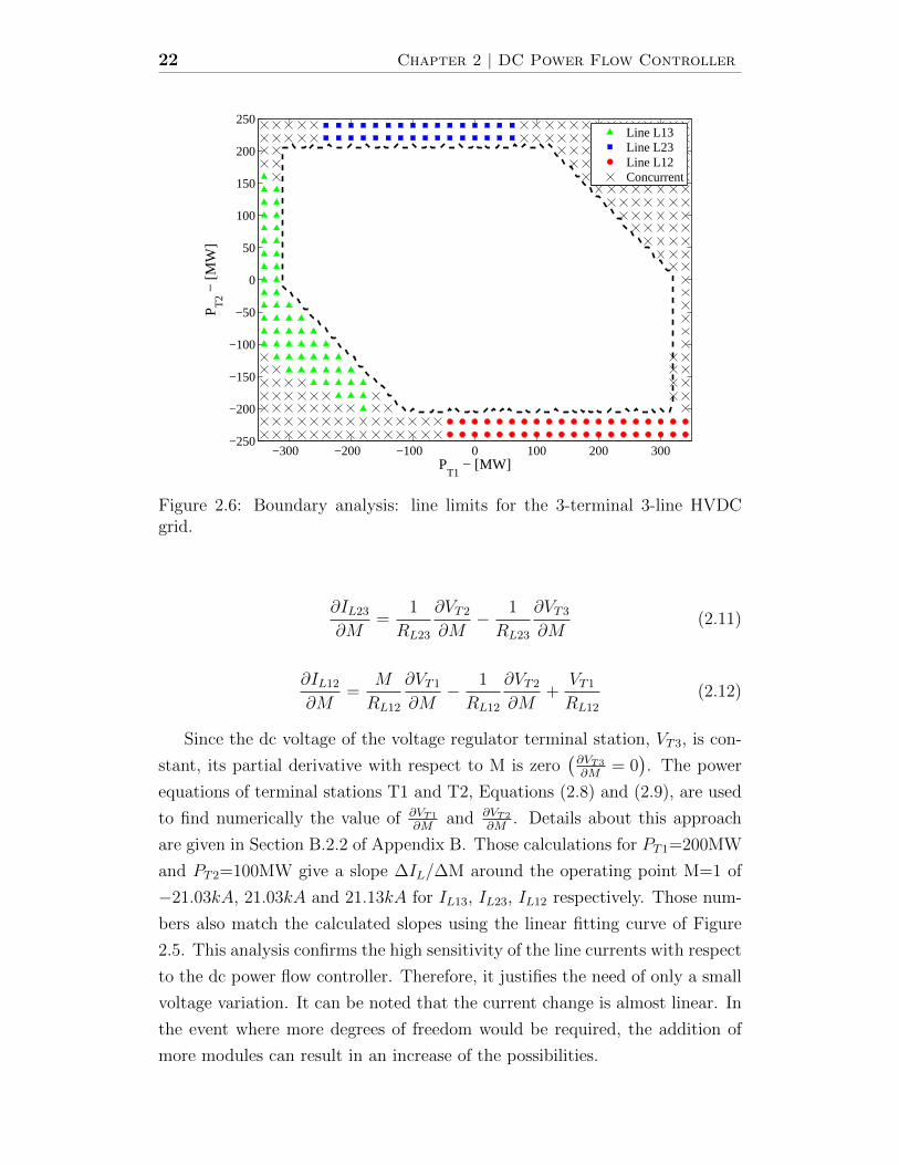
sponsible for the limits of the region of operation are shown in Figure 2.6. The
lines responsible for the boundary are identified and in the event of concurrent
exceeding lines, an “×” is used.
2.2.4 Current Sensitivity
As stated previously, line currents are very sensitive to the ratio M. As shown
in Figure 2.5, a variation of only 1% in the ratio M produces a change of
around 20% in the three currents. More precisely, the current sensitivity can
be calculated by doing the partial derivative of the current Equations (2.1),
(2.2) and (2.7). The results are shown in Equations (2.10), (2.11) and (2.12).
∂IL13
∂M=
1
RL13
∂VT1
∂M− 1
RL13
∂VT3
∂M(2.10)
22 Chapter 2 | DC Power Flow Controller
−300 −200 −100 0 100 200 300−250
−200
−150
−100
−50
0
50
100
150
200
250
PT1
− [MW]
P T2 −
[MW
]
Line L13Line L23Line L12Concurrent
Figure 2.6: Boundary analysis: line limits for the 3-terminal 3-line HVDCgrid.
∂IL23
∂M=
1
RL23
∂VT2
∂M− 1
RL23
∂VT3
∂M(2.11)
∂IL12
∂M=
M
RL12
∂VT1
∂M− 1
RL12
∂VT2
∂M+
VT1
RL12
(2.12)
Since the dc voltage of the voltage regulator terminal station, VT3, is con-
stant, its partial derivative with respect to M is zero(∂VT3
∂M= 0). The power
equations of terminal stations T1 and T2, Equations (2.8) and (2.9), are used
to find numerically the value of ∂VT1
∂Mand ∂VT2
∂M. Details about this approach
are given in Section B.2.2 of Appendix B. Those calculations for PT1=200MW
and PT2=100MW give a slope ∆IL/∆M around the operating point M=1 of
−21.03kA, 21.03kA and 21.13kA for IL13, IL23, IL12 respectively. Those num-
bers also match the calculated slopes using the linear fitting curve of Figure
2.5. This analysis confirms the high sensitivity of the line currents with respect
to the dc power flow controller. Therefore, it justifies the need of only a small
voltage variation. It can be noted that the current change is almost linear. In
the event where more degrees of freedom would be required, the addition of
more modules can result in an increase of the possibilities.

Concept and Benefits | 23
0.97 0.98 0.99 1 1.01 1.02 1.03
1.5
2
2.5
3
3.5
4
4.5
5
5.5
6
M
P loss
− [M
W]
PT1
=200MW
PT1
=160MW
PT1
=120MW
Figure 2.7: Transmission losses with respect to M for the 3-terminal 3-lineHVDC grid with PT2 = 100MW .
2.2.5 Transmission Losses
Since the dc power flow controller changes the line currents, it also influences
transmission losses. Figure 2.7 shows the transmission losses with respect to
the ratio M for a fixed power injection from terminal station T2 with three
different values for terminal station T1. It is expected that the lowest point is
at M=1 (or when no dc power flow controller is inserted) since, from circuit
theory, electrons naturally go through lowest resistance. However, because of
transmission line limits, such operating point (M=1) might not always be pos-
sible. In Figure 2.7, the continuous lines with markers are the operable region.
In all three cases, it is not possible to operate at minimal losses with M=1.
Nevertheless, it is possible to adjust M in order to minimize the transmission
losses but it seems to be a very limited application.
2.3 4-Terminal HVDC Grid
A similar analysis is performed to a HVDC grid with four terminal stations as
suggested in [10]. The initial 4-terminal system is composed of four transmis-
sion lines system as shown in Figure 2.8(a). The scenario is described as three
terminal stations (T1,T2,T4) supplying power to one voltage regulator point
(T3). Terminal stations T1, T2 and T4 supply 100MW each which gives a to-
tal of 300MW injected to terminal station T3 (neglecting transmission losses).
The results for that scenario are given in Table 2.4. The line current capacities

24 Chapter 2 | DC Power Flow Controller
Line L12
T3
T2T1
T4
LineL23
LineL41
Line L34
VT3=250kV
(a) 4-Line HVDC grid.
MLineL13
Line L12
T3
T2T1
T4
LineL23
LineL41
Line L34
VT3=250kV
(b) 5-Line HVDC grid.
Figure 2.8: MTDC grid configurations with 4 terminal stations.
Table 2.3: 4-Terminals - transmission line parameters.Transmission Distance Resistance Current Limits
Line [km] [Ω] [kA]
L12 248 3 0.25L23 165 2 0.7L34 165 2 0.6L41 413 5 0.2L13 248 3 0.5
are listed Table 2.3. Details and references about the transmission line models
are found in Section C.3 of Appendix C.
A fifth line with a dc power flow controller is added to the HVDC grid
between terminal stations T1 and T3 as shown in Figure 2.8(b). By adjusting
the ratio M to 1.002, it is possible to divert almost all the current injected by
terminal station T1 to line L13. Results are shown in Table 2.4. The set of
equation for calculation about this system is given in Section B.3 of Appendix
B.
In this section, only the region of operation and the current sensitivity are
analyzed due to the increase of complexity generated by the augmented grid
size.
Concept and Benefits | 25
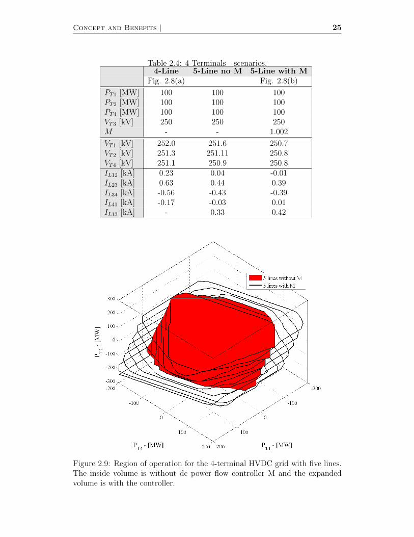
Table 2.4: 4-Terminals - scenarios.4-Line 5-Line no M 5-Line with M
Fig. 2.8(a) Fig. 2.8(b)
PT1 [MW] 100 100 100PT2 [MW] 100 100 100PT4 [MW] 100 100 100VT3 [kV] 250 250 250M - - 1.002
VT1 [kV] 252.0 251.6 250.7VT2 [kV] 251.3 251.11 250.8VT4 [kV] 251.1 250.9 250.8IL12 [kA] 0.23 0.04 -0.01IL23 [kA] 0.63 0.44 0.39IL34 [kA] -0.56 -0.43 -0.39IL41 [kA] -0.17 -0.03 0.01IL13 [kA] - 0.33 0.42
Figure 2.9: Region of operation for the 4-terminal HVDC grid with five lines.The inside volume is without dc power flow controller M and the expandedvolume is with the controller.
26 Chapter 2 | DC Power Flow Controller
−250 −200 −150 −100 −50 0 50 100 150 200 250−200
−150
−100
−50
0
50
100
150
200
250
300
PT1
− [MW]
P T4 −
[MW
]
5 Lines without M5 Lines with M
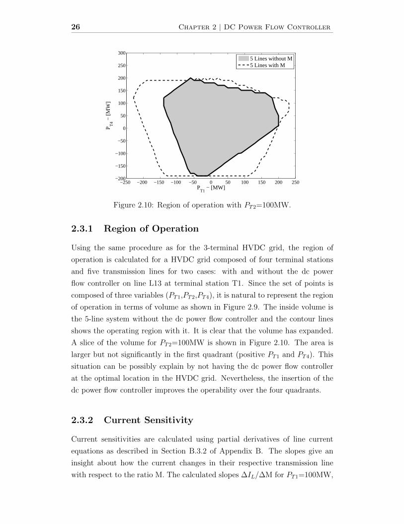
Figure 2.10: Region of operation with PT2=100MW.
2.3.1 Region of Operation
Using the same procedure as for the 3-terminal HVDC grid, the region of
operation is calculated for a HVDC grid composed of four terminal stations
and five transmission lines for two cases: with and without the dc power
flow controller on line L13 at terminal station T1. Since the set of points is
composed of three variables (PT1,PT2,PT4), it is natural to represent the region
of operation in terms of volume as shown in Figure 2.9. The inside volume is
the 5-line system without the dc power flow controller and the contour lines
shows the operating region with it. It is clear that the volume has expanded.
A slice of the volume for PT2=100MW is shown in Figure 2.10. The area is
larger but not significantly in the first quadrant (positive PT1 and PT4). This
situation can be possibly explain by not having the dc power flow controller
at the optimal location in the HVDC grid. Nevertheless, the insertion of the
dc power flow controller improves the operability over the four quadrants.
2.3.2 Current Sensitivity
Current sensitivities are calculated using partial derivatives of line current
equations as described in Section B.3.2 of Appendix B. The slopes give an
insight about how the current changes in their respective transmission line
with respect to the ratio M. The calculated slopes ∆IL/∆M for PT1=100MW,
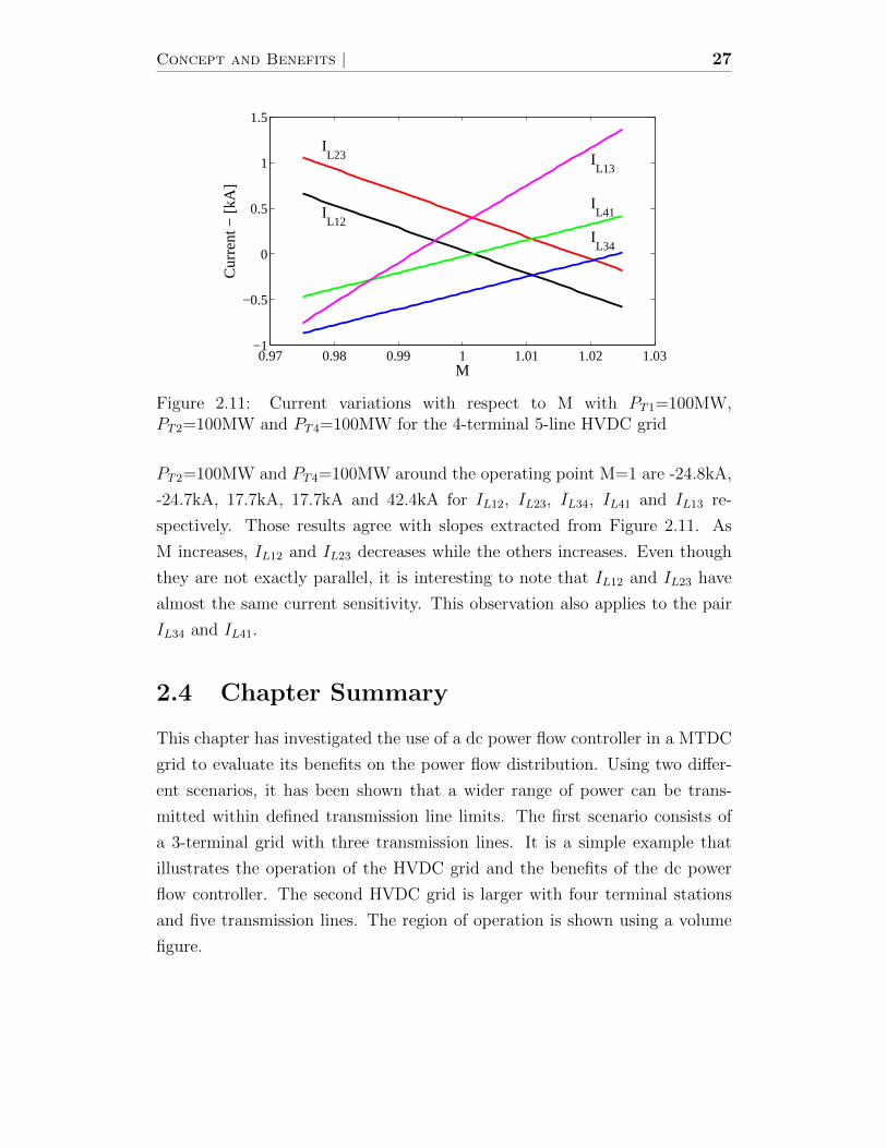
Concept and Benefits | 27
0.97 0.98 0.99 1 1.01 1.02 1.03−1
−0.5
0
0.5
1
1.5
IL12
IL23
IL34
IL41
IL13
M
Cur
rent
− [k
A]
Figure 2.11: Current variations with respect to M with PT1=100MW,PT2=100MW and PT4=100MW for the 4-terminal 5-line HVDC grid
PT2=100MW and PT4=100MW around the operating point M=1 are -24.8kA,
-24.7kA, 17.7kA, 17.7kA and 42.4kA for IL12, IL23, IL34, IL41 and IL13 re-
spectively. Those results agree with slopes extracted from Figure 2.11. As
M increases, IL12 and IL23 decreases while the others increases. Even though
they are not exactly parallel, it is interesting to note that IL12 and IL23 have
almost the same current sensitivity. This observation also applies to the pair
IL34 and IL41.
2.4 Chapter Summary
This chapter has investigated the use of a dc power flow controller in a MTDC
grid to evaluate its benefits on the power flow distribution. Using two differ-
ent scenarios, it has been shown that a wider range of power can be trans-
mitted within defined transmission line limits. The first scenario consists of
a 3-terminal grid with three transmission lines. It is a simple example that
illustrates the operation of the HVDC grid and the benefits of the dc power
flow controller. The second HVDC grid is larger with four terminal stations
and five transmission lines. The region of operation is shown using a volume
figure.

28 Chapter 2 | DC Power Flow Controller

Chapter 3
DC Power Flow Controller:
Hardware Realization and
Implementation
In the previous chapter, it has been shown that the domain of power flow
controllability is enlarged by dc power flow controllers. The next step is to
develop the hardware realization. This chapter presents the circuitry, controls
and simulations as proof of principle.
The possible forms of dc power flow controller are examined. From the
examination, a thyristor-based controller is adopted for implementation. Sim-
ulation results are obtained to evaluate the performance of such dc power flow
controller.
3.1 Configuration
In designing a dc power flow controller, one looks to Flexible AC Transmission
System (FACTS) for guidance. In general, controllers of FACTS derive their
flexibility by managing reactive powers. But there is no reactive power in the
HVDC grid to manage. Therefore, the dc power flow controller must manage
by inverting (or rectifying) active real power to (or from) the ac-side. This does
not affect the efficiency (except for ohmic losses in the components) because
the rectified (or inverted) ac power is taken from (or returned) to the ac-side.
The dc power flow controller is treated as an appendage of a VSC-HVDC
station. The VSC-HVDC provides the dc voltage lift, for example to VT1 =
29

30 Chapter 3 | DC Power Flow Controller
AC
DC
+
-
DCPowerFlow
ControllerVT1
VT1
Line1
Line 2
+
-
(a) Shunt controller.
AC
DC
+
-
VT1
VT1=VT1+Vx
Line1
Line 2
-
+Vx
+
-
DCPower Flow
Controller
(b) Series controller.
Figure 3.1: DC Power Flow Controller: (a) shunt; and (b) series.
250kVDC, and the dc power flow controller provides a continuous variation
within 5%(±2.5%), so that the range of controllable dc voltage in the exam-
ple is 244kV ≤ VT1 ≤ 256kV . As shown in the previous chapter, the dc
transmission line resistance is low, therefore, a small change in the dc voltage
generates a significant dc current variation. Two types of connection are pos-
sible for such controller: shunt connected, shown in Figure 3.1(a), and series
connected, shown in Figure 3.1(b).
3.1.1 Shunt Connected
The shunt controller in Figure 3.1(a) is essentially a dc-dc transformer with
input/output voltages bearing the relation:
VT1 = MVT1 (3.1)
where M is the voltage transformer ratio as defined in the previous chapter.
DC-DC transformers are widely used in low power electronics. A recent
proposal for high power applications is based on resonant converters [66]. How-
ever, the design of [66] is to step-up voltages from 22kV to 250kV. In dc power
flow controller application, the desired voltage step-up ratio is of the order of
M=0.975 to 1.025. Therefore, the design of [66] has not been pursued for this
application.
Another objection is that VT1, the voltage output of the controller, must
be rated at around dc line voltage. As line current is also around 1pu, the
MVA rating of the shunt controller is of the order of 100% and not 5%.
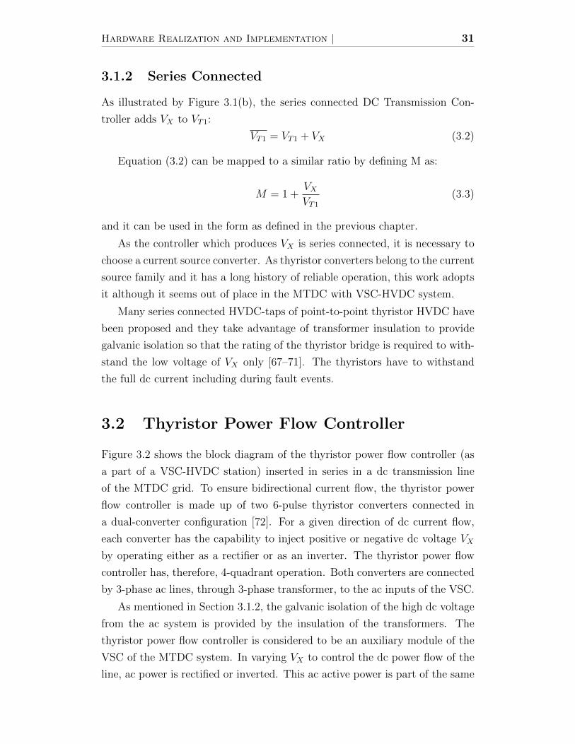
Hardware Realization and Implementation | 31
3.1.2 Series Connected
As illustrated by Figure 3.1(b), the series connected DC Transmission Con-
troller adds VX to VT1:
VT1 = VT1 + VX (3.2)
Equation (3.2) can be mapped to a similar ratio by defining M as:
M = 1 +VXVT1
(3.3)
and it can be used in the form as defined in the previous chapter.
As the controller which produces VX is series connected, it is necessary to
choose a current source converter. As thyristor converters belong to the current
source family and it has a long history of reliable operation, this work adopts
it although it seems out of place in the MTDC with VSC-HVDC system.
Many series connected HVDC-taps of point-to-point thyristor HVDC have
been proposed and they take advantage of transformer insulation to provide
galvanic isolation so that the rating of the thyristor bridge is required to with-
stand the low voltage of VX only [67–71]. The thyristors have to withstand
the full dc current including during fault events.
3.2 Thyristor Power Flow Controller
Figure 3.2 shows the block diagram of the thyristor power flow controller (as
a part of a VSC-HVDC station) inserted in series in a dc transmission line
of the MTDC grid. To ensure bidirectional current flow, the thyristor power
flow controller is made up of two 6-pulse thyristor converters connected in
a dual-converter configuration [72]. For a given direction of dc current flow,
each converter has the capability to inject positive or negative dc voltage VX
by operating either as a rectifier or as an inverter. The thyristor power flow
controller has, therefore, 4-quadrant operation. Both converters are connected
by 3-phase ac lines, through 3-phase transformer, to the ac inputs of the VSC.
As mentioned in Section 3.1.2, the galvanic isolation of the high dc voltage
from the ac system is provided by the insulation of the transformers. The
thyristor power flow controller is considered to be an auxiliary module of the
VSC of the MTDC system. In varying VX to control the dc power flow of the
line, ac power is rectified or inverted. This ac active power is part of the same
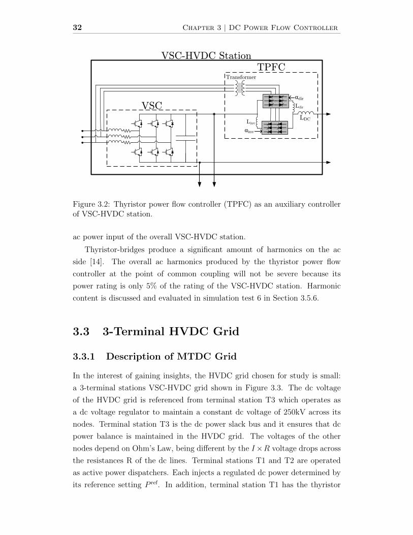
32 Chapter 3 | DC Power Flow Controller
dir
inv
VSC
TPFC
Linv
Ldir
LDC
Transformer
VSC-HVDC Station
Figure 3.2: Thyristor power flow controller (TPFC) as an auxiliary controllerof VSC-HVDC station.
ac power input of the overall VSC-HVDC station.
Thyristor-bridges produce a significant amount of harmonics on the ac
side [14]. The overall ac harmonics produced by the thyristor power flow
controller at the point of common coupling will not be severe because its
power rating is only 5% of the rating of the VSC-HVDC station. Harmonic
content is discussed and evaluated in simulation test 6 in Section 3.5.6.
3.3 3-Terminal HVDC Grid
3.3.1 Description of MTDC Grid
In the interest of gaining insights, the HVDC grid chosen for study is small:
a 3-terminal stations VSC-HVDC grid shown in Figure 3.3. The dc voltage
of the HVDC grid is referenced from terminal station T3 which operates as
a dc voltage regulator to maintain a constant dc voltage of 250kV across its
nodes. Terminal station T3 is the dc power slack bus and it ensures that dc
power balance is maintained in the HVDC grid. The voltages of the other
nodes depend on Ohm’s Law, being different by the I×R voltage drops across
the resistances R of the dc lines. Terminal stations T1 and T2 are operated
as active power dispatchers. Each injects a regulated dc power determined by
its reference setting P ref. In addition, terminal station T1 has the thyristor
Hardware Realization and Implementation | 33
PT1
160MW
Terminal Station T1
VT3DC
Terminal Station T3
Terminal Station T2
IL13
IL12
IL23
+
-VX
+
-
PT2
80MW
250kV
Figure 3.3: Multiterminal HVDC formed from 3 VSC terminal stations.
Table 3.1: System parameters.DC Cable Parameters Line L13 Line L23 Line L12Distance [km] 248 83 165Resistance [Ω] 3 1 2Inductance [mH] 26.2 8.8 17.4
VSC Parameters VSC T1 VSC T2 VSC T3AC Voltage [kV] 83 83 83AC Frequency [Hz] 50 50 50DC Capacitor [mF] 0.2 0.2 0.4Switching Frequency [kHz] 1.5 1.5 1.5
Thyristor Power Flow ControllerDC inductance LDC [mH] 100DC inductance Ldir, Linv [mH] 50
power flow controller to inject VX in line L12. For simulation tests, the trans-
mission line parameters are given in Table 3.1. Details and references about
the transmission line model can be found in Section C.3 of Appendix C.
3.3.2 Preliminary Design to Rate Thyristor Power Flow
Controller
The design of the thyristor power flow controller requires computation of the
voltages VT1, VT2 and VT3 of terminal stations T1, T2 and T3 and the dc
currents of lines L12, L13 and L23. The rated power for terminal stations
T1 and T2 are chosen to be 160MW and 80MW, respectively. The thyristor

34 Chapter 3 | DC Power Flow Controller
−5 −4 −3 −2 −1 0 1 2 3 4 5−1
−0.5
0
0.5
1
1.5
I LIN
E −
[kA
]
IL13
IL23
IL12
−5 −4 −3 −2 −1 0 1 2 3 4 5248
249
250
251
252
253
254
VX
− [kV]
VT
ER
MIN
AL −
[kV
]
VT1
VT2
VT3
Figure 3.4: Line currents-vs-VX and Node voltages-vs-VX for PT1 = 160MWand PT2 = 80MW
power flow controller is designed to inject a voltage which varies from -5kV to
+5kV. Using the same algorithm described in Appendix B, the computed line
currents and the terminal dc voltages are shown in Figure 3.4. As VX increases,
a portion of current in the line L13 is redirected to terminal station T3 via
the route L12-L23. The largest current which flows in line L12 is 1.1kA when
VX=+5kV. Therefore, each converter of the thyristor power flow controller
should be rated for 5.5MW. The dual-converters require 11.0MW which is less
than 7% of the 160MW rated converter of terminal station T1. The maximum
current rating is 1.1kA.
3.4 Implementation of Control
As the thyristor power flow controller of Figure 3.2 is tested and evaluated in
the MTDC system of Figure 3.3, it is necessary to describe briefly the controls
of the VSC station and the thyristor power flow controller.
Hardware Realization and Implementation | 35
Table 3.2: Mode of operation of converters.d-axis controller q-axis controller
VSC T1 Power Reactive current(rectifier)VSC T2 Power Reactive current(rectifier)VSC T3 DC voltage Reactive current
(inverter) 250kV
TPFC Current Control
3.4.1 Voltage Source Converter (VSC) Station
The operation of VSC is well known and the dq-controller approach is used in
this thesis. The VSC model and the control structure are described in Section
C.1 of Appendix C. Detailed parameters of the VSC used in this chapter are
given in Section C.4 but the main parameters are listed in Table 3.1.
The modes of operation of the VSCs are summarized in Table 3.2. Terminal
stations T1 and T2 are under constant active power control and terminal
station T3 is in dc voltage regulator mode. The setting of q-axis current
control is irefq =0.0 for all VSCs.
3.4.2 Operation of Thyristor Power Flow Controller
The thyristor power flow controller is composed of two thyristor-bridges that
are connected back-to-back as shown in Figure 3.5. Each bridge allows only
unidirectional dc current flow [14,72]. Its dc output voltage Vd can be positive
or negative depending on the firing angle α1 in the equation:
Vd =3√
2
πVac cos(α1) (3.4)
where Vac is the rms value of the line-to-line voltage from the transformer.
Figure 3.6 shows Vd as a function of α1 under the label “direct”. For 0 ≤α1 ≤ 90, Vd is positive and the converter is rectifying. 90 ≤ α1 ≤ 180,
Vd is negative and the converter is inverting. Each bridge is capable of only
2-quadrant operation.
A second converter is required to enable the dc current to flow in the oppo-
site direction. The Vd-vs-α1 relationship of the second converter is labeled “in-
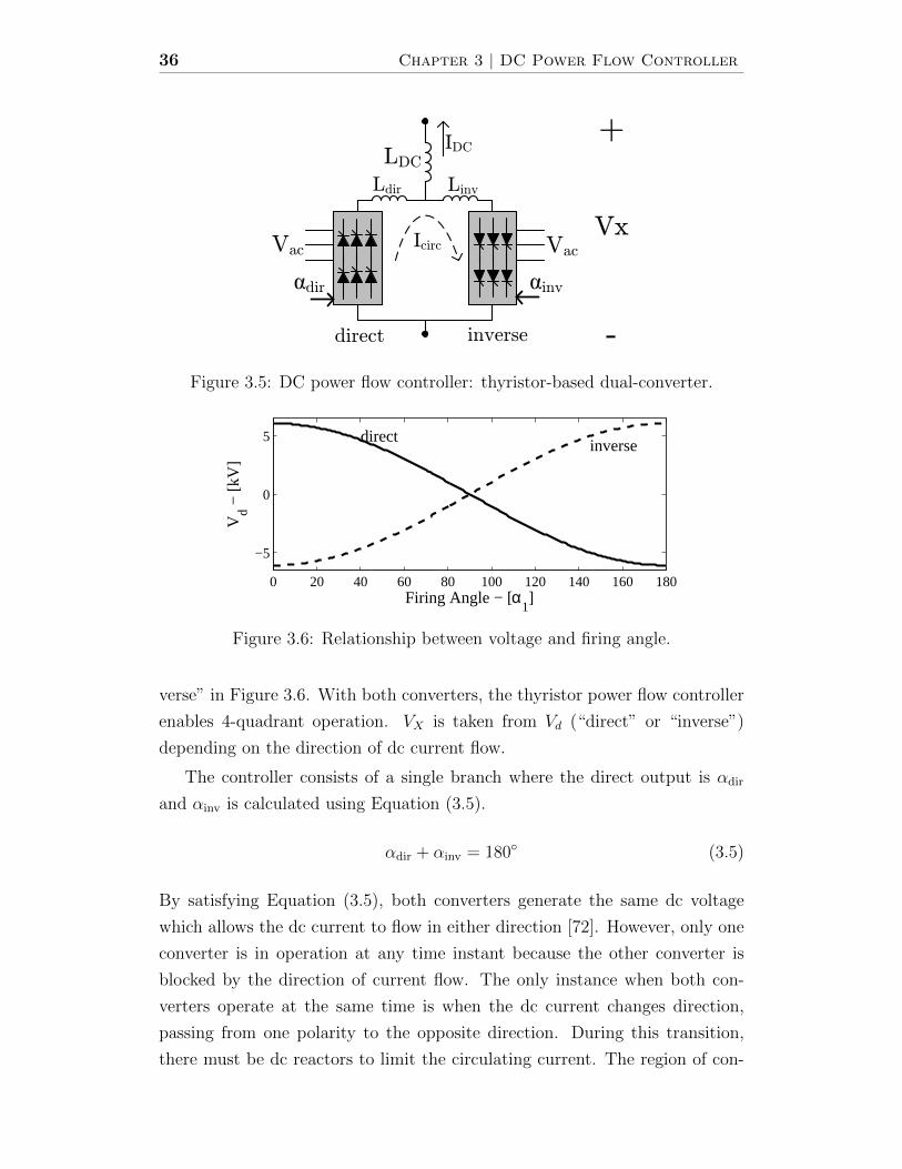
36 Chapter 3 | DC Power Flow Controller
dir inv
LinvLdir
LDC
Vac Vac
IDC+
-
VxIcirc
direct inverse
Figure 3.5: DC power flow controller: thyristor-based dual-converter.
0 20 40 60 80 100 120 140 160 180
−5
0
5 directinverse
Vd −
[kV
]
Firing Angle − [α1]
Figure 3.6: Relationship between voltage and firing angle.
verse” in Figure 3.6. With both converters, the thyristor power flow controller
enables 4-quadrant operation. VX is taken from Vd (“direct” or “inverse”)
depending on the direction of dc current flow.
The controller consists of a single branch where the direct output is αdir
and αinv is calculated using Equation (3.5).
αdir + αinv = 180 (3.5)
By satisfying Equation (3.5), both converters generate the same dc voltage
which allows the dc current to flow in either direction [72]. However, only one
converter is in operation at any time instant because the other converter is
blocked by the direction of current flow. The only instance when both con-
verters operate at the same time is when the dc current changes direction,
passing from one polarity to the opposite direction. During this transition,
there must be dc reactors to limit the circulating current. The region of con-
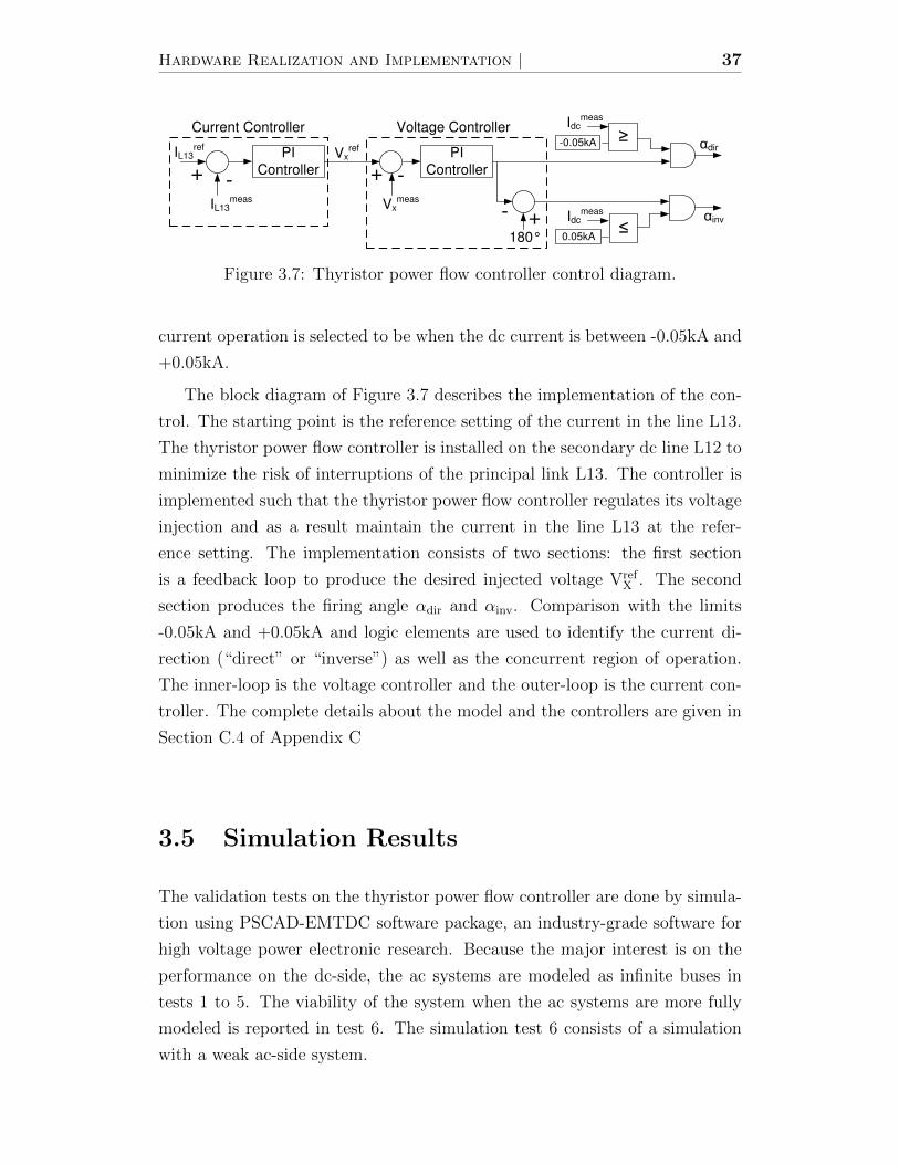
Hardware Realization and Implementation | 37
PI
Controller
PI
Controller + -+ -
IL13ref
IL13meas Vx
meas
+-180°
dir
inv
Vxref
Voltage ControllerCurrent Controller-0.05kA
Idcmeas
0.05kA
Idcmeas
Figure 3.7: Thyristor power flow controller control diagram.
current operation is selected to be when the dc current is between -0.05kA and
+0.05kA.
The block diagram of Figure 3.7 describes the implementation of the con-
trol. The starting point is the reference setting of the current in the line L13.
The thyristor power flow controller is installed on the secondary dc line L12 to
minimize the risk of interruptions of the principal link L13. The controller is
implemented such that the thyristor power flow controller regulates its voltage
injection and as a result maintain the current in the line L13 at the refer-
ence setting. The implementation consists of two sections: the first section
is a feedback loop to produce the desired injected voltage VrefX . The second
section produces the firing angle αdir and αinv. Comparison with the limits
-0.05kA and +0.05kA and logic elements are used to identify the current di-
rection (“direct” or “inverse”) as well as the concurrent region of operation.
The inner-loop is the voltage controller and the outer-loop is the current con-
troller. The complete details about the model and the controllers are given in
Section C.4 of Appendix C
3.5 Simulation Results
The validation tests on the thyristor power flow controller are done by simula-
tion using PSCAD-EMTDC software package, an industry-grade software for
high voltage power electronic research. Because the major interest is on the
performance on the dc-side, the ac systems are modeled as infinite buses in
tests 1 to 5. The viability of the system when the ac systems are more fully
modeled is reported in test 6. The simulation test 6 consists of a simulation
with a weak ac-side system.
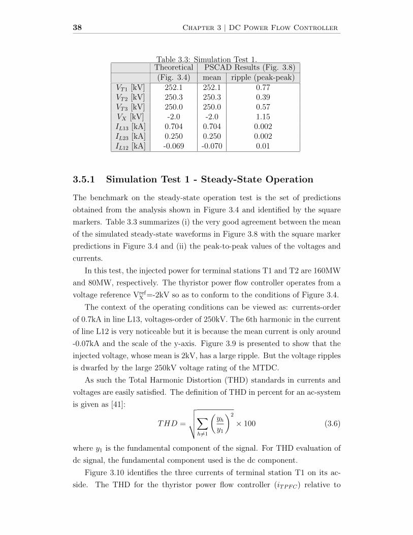
38 Chapter 3 | DC Power Flow Controller
Table 3.3: Simulation Test 1.Theoretical PSCAD Results (Fig. 3.8)(Fig. 3.4) mean ripple (peak-peak)
VT1 [kV] 252.1 252.1 0.77VT2 [kV] 250.3 250.3 0.39VT3 [kV] 250.0 250.0 0.57VX [kV] -2.0 -2.0 1.15IL13 [kA] 0.704 0.704 0.002IL23 [kA] 0.250 0.250 0.002IL12 [kA] -0.069 -0.070 0.01
3.5.1 Simulation Test 1 - Steady-State Operation
The benchmark on the steady-state operation test is the set of predictions
obtained from the analysis shown in Figure 3.4 and identified by the square
markers. Table 3.3 summarizes (i) the very good agreement between the mean
of the simulated steady-state waveforms in Figure 3.8 with the square marker
predictions in Figure 3.4 and (ii) the peak-to-peak values of the voltages and
currents.
In this test, the injected power for terminal stations T1 and T2 are 160MW
and 80MW, respectively. The thyristor power flow controller operates from a
voltage reference VrefX =-2kV so as to conform to the conditions of Figure 3.4.
The context of the operating conditions can be viewed as: currents-order
of 0.7kA in line L13, voltages-order of 250kV. The 6th harmonic in the current
of line L12 is very noticeable but it is because the mean current is only around
-0.07kA and the scale of the y-axis. Figure 3.9 is presented to show that the
injected voltage, whose mean is 2kV, has a large ripple. But the voltage ripples
is dwarfed by the large 250kV voltage rating of the MTDC.
As such the Total Harmonic Distortion (THD) standards in currents and
voltages are easily satisfied. The definition of THD in percent for an ac-system
is given as [41]:
THD =
√√√√∑h6=1
(yhy1
)2
× 100 (3.6)
where y1 is the fundamental component of the signal. For THD evaluation of
dc signal, the fundamental component used is the dc component.
Figure 3.10 identifies the three currents of terminal station T1 on its ac-
side. The THD for the thyristor power flow controller (iTPFC) relative to
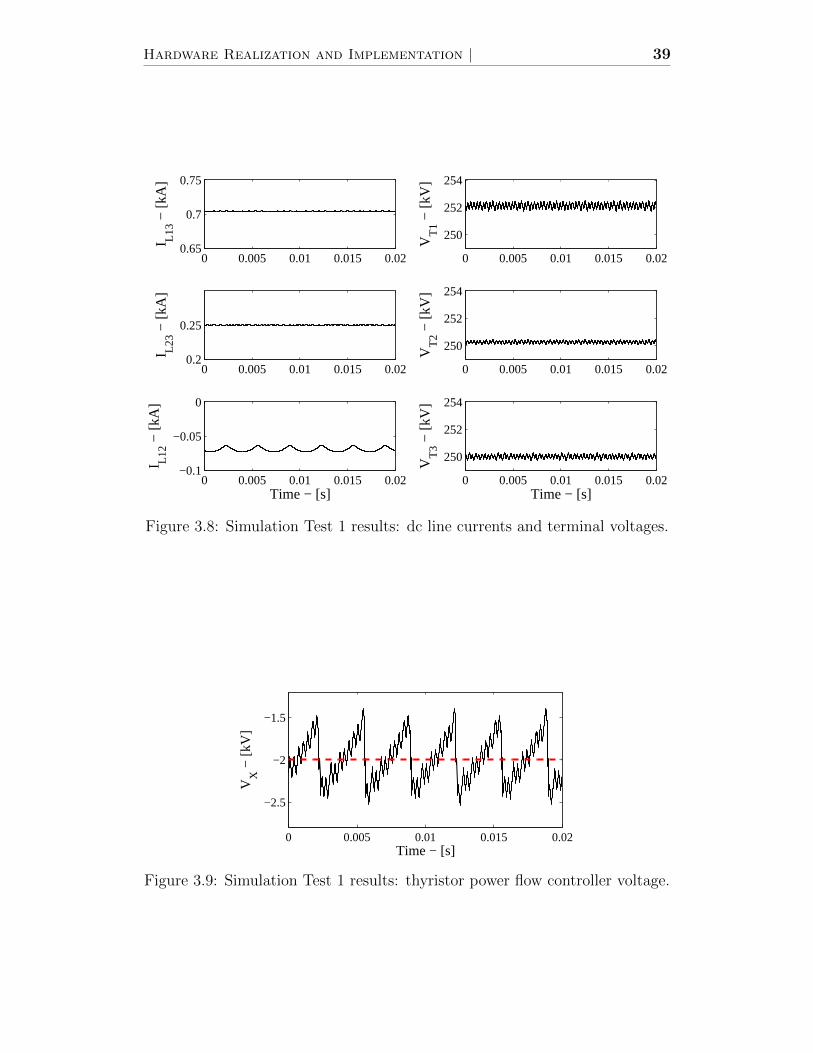
Hardware Realization and Implementation | 39
0 0.005 0.01 0.015 0.020.65
0.7
0.75
I L13 −
[kA
]
0 0.005 0.01 0.015 0.020.2
0.25
I L23 −
[kA
]
0 0.005 0.01 0.015 0.02−0.1
−0.05
0
I L12 −
[kA
]
Time − [s]
0 0.005 0.01 0.015 0.02
250
252
254
VT
1 − [k
V]
0 0.005 0.01 0.015 0.02
250
252
254
VT
2 − [k
V]
0 0.005 0.01 0.015 0.02
250
252
254
VT
3 − [k
V]
Time − [s]
Figure 3.8: Simulation Test 1 results: dc line currents and terminal voltages.
0 0.005 0.01 0.015 0.02
−2.5
−2
−1.5
VX
− [k
V]
Time − [s]
Figure 3.9: Simulation Test 1 results: thyristor power flow controller voltage.
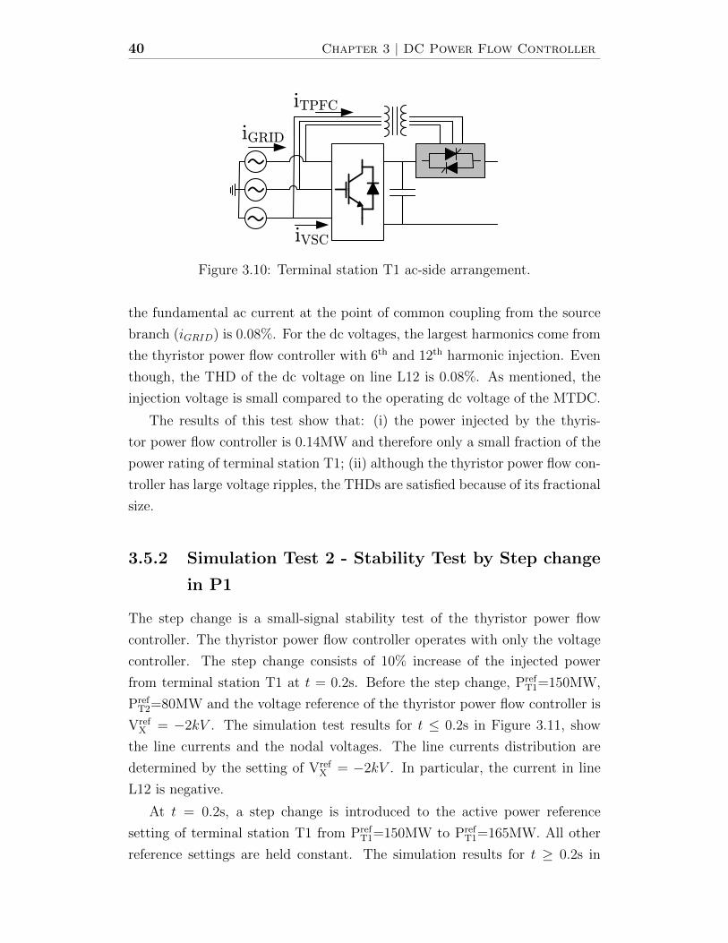
40 Chapter 3 | DC Power Flow Controller
~~~
iGRID
iTPFC
iVSC
Figure 3.10: Terminal station T1 ac-side arrangement.
the fundamental ac current at the point of common coupling from the source
branch (iGRID) is 0.08%. For the dc voltages, the largest harmonics come from
the thyristor power flow controller with 6th and 12th harmonic injection. Even
though, the THD of the dc voltage on line L12 is 0.08%. As mentioned, the
injection voltage is small compared to the operating dc voltage of the MTDC.
The results of this test show that: (i) the power injected by the thyris-
tor power flow controller is 0.14MW and therefore only a small fraction of the
power rating of terminal station T1; (ii) although the thyristor power flow con-
troller has large voltage ripples, the THDs are satisfied because of its fractional
size.
3.5.2 Simulation Test 2 - Stability Test by Step change
in P1
The step change is a small-signal stability test of the thyristor power flow
controller. The thyristor power flow controller operates with only the voltage
controller. The step change consists of 10% increase of the injected power
from terminal station T1 at t = 0.2s. Before the step change, PrefT1=150MW,
PrefT2=80MW and the voltage reference of the thyristor power flow controller is
VrefX = −2kV . The simulation test results for t ≤ 0.2s in Figure 3.11, show
the line currents and the nodal voltages. The line currents distribution are
determined by the setting of VrefX = −2kV . In particular, the current in line
L12 is negative.
At t = 0.2s, a step change is introduced to the active power reference
setting of terminal station T1 from PrefT1=150MW to Pref
T1=165MW. All other
reference settings are held constant. The simulation results for t ≥ 0.2s in

Hardware Realization and Implementation | 41
0 0.5 1 1.5 2
0.68
0.7
0.72
I L13 −
[kA
]
0 0.5 1 1.5 20.22
0.24
0.26
0.28
I L23 −
[kA
]
0 0.5 1 1.5 2−0.1
−0.05
0
I L12 −
[kA
]
Time − [s]
0 0.5 1 1.5 2248250252254256
VT
1 − [k
V]
0 0.5 1 1.5 2248250252254256
VT
2 − [k
V]
0 0.5 1 1.5 2248250252254256
VT
3 − [k
V]
Time − [s]
Figure 3.11: Simulation Test 2 results: dc line currents and terminal voltages.
0 0.5 1 1.5 2
−2.04
−2.03
−2.02
−2.01
−2
−1.99
Vx −
[kV
]
Time − [s]
Figure 3.12: Simulation Test 2 results: Thyristor power flow controller voltage.
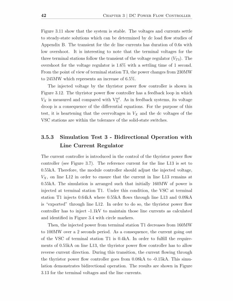
42 Chapter 3 | DC Power Flow Controller
Figure 3.11 show that the system is stable. The voltages and currents settle
to steady-state solutions which can be determined by dc load flow studies of
Appendix B. The transient for the dc line currents has duration of 0.6s with
low overshoot. It is interesting to note that the terminal voltages for the
three terminal stations follow the transient of the voltage regulator (VT3). The
overshoot for the voltage regulator is 1.6% with a settling time of 1 second.
From the point of view of terminal station T3, the power changes from 230MW
to 245MW which represents an increase of 6.5%.
The injected voltage by the thyristor power flow controller is shown in
Figure 3.12. The thyristor power flow controller has a feedback loop in which
VX is measured and compared with VrefX . As in feedback systems, its voltage
droop is a consequence of the differential equations. For the purpose of this
test, it is heartening that the overvoltages in VX and the dc voltages of the
VSC stations are within the tolerance of the solid-state switches.
3.5.3 Simulation Test 3 - Bidirectional Operation with
Line Current Regulator
The current controller is introduced in the control of the thyristor power flow
controller (see Figure 3.7). The reference current for the line L13 is set to
0.55kA. Therefore, the module controller should adjust the injected voltage,
VX , on line L12 in order to ensure that the current in line L13 remains at
0.55kA. The simulation is arranged such that initially 160MW of power is
injected at terminal station T1. Under this condition, the VSC at terminal
station T1 injects 0.64kA where 0.55kA flows through line L13 and 0.09kA
is “exported” through line L12. In order to do so, the thyristor power flow
controller has to inject -1.1kV to maintain those line currents as calculated
and identified in Figure 3.4 with circle markers.
Then, the injected power from terminal station T1 decreases from 160MW
to 100MW over a 2 seconds period. As a consequence, the current going out
of the VSC of terminal station T1 is 0.4kA. In order to fulfill the require-
ments of 0.55kA on line L13, the thyristor power flow controller has to allow
reverse current direction. During this transition, the current flowing through
the thyristor power flow controller goes from 0.08kA to -0.15kA. This simu-
lation demonstrates bidirectional operation. The results are shown in Figure
3.13 for the terminal voltages and the line currents.
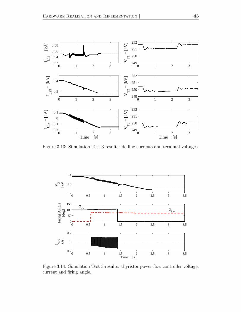
Hardware Realization and Implementation | 43
0 1 2 30.52
0.54
0.56
0.58I L1
3 − [k
A]
0 1 2 3
0.2
0.4
I L23 −
[kA
]
0 1 2 3−0.2
−0.1
0
0.1
I L12 −
[kA
]
Time − [s]
0 1 2 3249
250
251
252
VT
1 − [k
V]
0 1 2 3249
250
251
252
VT
2 − [k
V]
0 1 2 3249
250
251
252
VT
3 − [k
V]
Time − [s]
Figure 3.13: Simulation Test 3 results: dc line currents and terminal voltages.
0 0.5 1 1.5 2 2.5 3 3.5−2
−1.5
−1
VX
[kV
]
0 0.5 1 1.5 2 2.5 3 3.50
50
100
150
Firi
ng A
nlgl
e[d
eg]
αdir α
inv
0 0.5 1 1.5 2 2.5 3 3.5−0.2
0
0.2
I circ
[kA
]
Time − [s]
Figure 3.14: Simulation Test 3 results: thyristor power flow controller voltage,current and firing angle.
44 Chapter 3 | DC Power Flow Controller
The current in line L12 decreases and at 0.58s the thyristor power flow con-
troller enters in dual mode with circulating current. The overlap of the firing
angles is shown in Figure 3.14. During that period, both 6-pulse bridges oper-
ate simultaneous. The magnitude of the circulating current is ±0.2kA which
is within thyristor current ratings. During the transition the voltage reference
decreases to 249.4kV and as soon as the injected power PT1 is stabilized, the
voltage is back to 250kV within 1s.
This simulation explores the functionality of the current controller as well
as the bidirectional operation of the thyristor power flow controller. During the
transition period, the circulating current is observed. Its amplitude is limited
by dc reactors in each branch and it remains within tolerable boundaries.
3.5.4 Simulation Test 4 - Terminal Station Loss with
Line Current Regulator
This scenario is an abrupt shut down of the VSC at terminal station T2. The
thyristor power flow controller is implemented with the line current regulator.
At 0.2s, ac breakers at terminal station T2 opens and the firing pulses of the
VSC are blocked. From that point on, no energy conversion is performed
at terminal station T2 but the converter remains connected on the dc side
with the HVDC grid. No dc breaker nor disconnect switch are used in this
simulation.
As shown in Figure 3.15, large oscillations are produced on the line L23
from 0.2s to 0.6s. However, those oscillations remain positive. The reference
terminal voltage drops from 250kV to 230kV but regulates back within 0.6sec
and the overvoltage created by the recovery process is only of 4%. At terminal
station T3, this perturbation is a variation in the incoming power from 240MW
to 160MW which represents a loss of 33%. At 0.8s, the HVDC grid is back
in normal operation with only two converters. The current in line L13 is
regulated at 0.55kA and the link L12-L23 remains operational despite the fact
that terminal station T2 is out of service.
Figure 3.16 shows the voltage reference generated by the current controller,
VrefX , and how it influences the firing angle αdir. The behaviour of the MTDC
under the loss of one terminal station has been demonstrated in this simulation.
The HVDC grid remains stable and recovers from this perturbation.

Hardware Realization and Implementation | 45
0 0.2 0.4 0.6 0.8 1
0.5
0.6
0.7I L1
3 − [k
A]
0 0.2 0.4 0.6 0.8 10
0.5
I L23 −
[kA
]
0 0.2 0.4 0.6 0.8 10.05
0.1
0.15
I L12 −
[kA
]
Time − [s]
0 0.2 0.4 0.6 0.8 1230
240
250
260
VT
1 − [k
V]
0 0.2 0.4 0.6 0.8 1230
240
250
260
VT
2 − [k
V]
0 0.2 0.4 0.6 0.8 1230
240
250
260
VT
3 − [k
V]
Time − [s]
Figure 3.15: Simulation Test 4 results: dc line currents and terminal voltages.
0 0.2 0.4 0.6 0.8 1 1.2−1.8−1.6−1.4−1.2
−1
VXre
f − [k
V]
0 0.2 0.4 0.6 0.8 1 1.290
100
110
Firi
ng A
nlgl
e[d
eg]
Time − [s]
αdir
Figure 3.16: Simulation Test 4 results: thyristor power flow controller voltageand firing angle.

46 Chapter 3 | DC Power Flow Controller
3.5.5 Simulation Test 5 - Operation with Positive VX
This simulation test demonstrates the operation of the thyristor power flow
controller with positive voltage injection. The reference current value is set to
zero for the line current L13. By doing so, all the power produced by terminal
station T1 is forced to transmit via line L23. The required injected voltage is
established at 2.25kV as displayed in Figure 3.4 with triangle markers. The
steady-state operation results are shown in Figure 3.17. The injected voltage
is shown in Figure 3.18 with an average of 2.25kV.
The system is stable and the terminal voltage ripple is less than 0.2%. The
current flowing in the thyristor power flow controller is 0.64kA which is in the
upper limit range of operation according the results given in Figure 3.4.
The test demonstrates the operation of the thyristor power flow controller
in the first-quadrant operation. The system is able to divert almost all the
current from flowing in line L13. Such operating point can be used when a
line needs to be smoothly disconnected, in a maintenance routine for example.
3.5.6 Simulation Test 6 - Weak AC System
VSC does not depend on strong ac system to operate. However, thyristor-
based converter is sensitive to the strength of the ac grid. Weak ac system
can lead to commutation failures of the thyristor-based converter [73]. The
operation of the system is evaluated when VSC at terminal station T1 is
connected to a weak ac system as shown in Figure 3.19. The setting points
are PrefT1 = 160MW , Pref
T2 = 80MW and the voltage reference of the thyristor
power flow controller is VrefX = −2kV .
The short-circuit ratio (SCR) is used to determine if an ac system is weak
or strong. Possible problems related to weak ac system includes commutation
failure, harmonic resonance and instability. It is defined as [73]:
SCR =V 2ac
PdcZac(3.7)
where Vac is the line-to-line rms ac voltage at the point of common coupling
(PCC), Pdc is the dc power transmitted and Zac is ac impedance of the source.
In general, weak ac system has a short-circuit ratio (SCR) lower than 2. For
VRMSLL =83kV and Pdc=160MW, a short-circuit ratio of 1.9 gives a line induc-
tance Lac of 72mH.
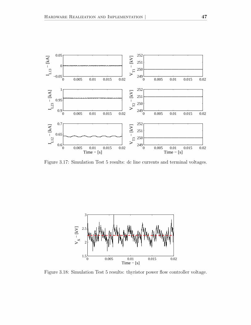
Hardware Realization and Implementation | 47
0 0.005 0.01 0.015 0.02−0.05
0
0.05
I L13 −
[kA
]
0 0.005 0.01 0.015 0.020.9
0.95
1
I L23 −
[kA
]
0 0.005 0.01 0.015 0.020.6
0.65
0.7
I L12 −
[kA
]
Time − [s]
0 0.005 0.01 0.015 0.02249
250
251
252
VT
1 − [k
V]
0 0.005 0.01 0.015 0.02249
250
251
252
VT
2 − [k
V]
0 0.005 0.01 0.015 0.02249
250
251
252
VT
3 − [k
V]
Time − [s]
Figure 3.17: Simulation Test 5 results: dc line currents and terminal voltages.
0 0.005 0.01 0.015 0.021.5
2
2.5
3
VX
− [k
V]
Time − [s]
Figure 3.18: Simulation Test 5 results: thyristor power flow controller voltage.

48 Chapter 3 | DC Power Flow Controller
As shown in Figure 3.19, a three-phase series RLC filter tuned to filter the
harmonic content around the switching frequency is connected at the point
of common coupling (PCC) [74]. Filter parameters are Cf=5uF, Lf=2.3mH
and Rf=2Ω. By including the harmonic filter, the effective short-circuit ratio
(ESCR), given in Equation (3.8), becomes 1.97. In addition to the filter, the
q-axis reference of the VSC controller provides ac voltage support. In this
scenario, irefq is set to 1.25kA.
ESCR =
(1
Zac+
1
Zf
)V 2ac
Pdc(3.8)
where Zf is the impedance of the harmonic filter.
The combined actions of the ac filter and the q-axis controller are effective
and the THD is reduced to 2.45%. The voltage waveform at the point of
common coupling is shown in Figure 3.20(a). The harmonic content of the
voltage is shown in Figure 3.20(b). The magnitude is expressed as a ratio with
respect to the magnitude at the fundamental frequency of the system (50Hz).
All individual harmonics are below 1.25%.
From the 6-pulse thyristor-bridge of Figure 3.5, the ac harmonics are the
5th and the 7th. They are noticeable in Figure 3.20(b). The other harmonics
are the well known side-bands of the triangular carrier frequency (1.5kHz) of
the sinusoidal pulse width modulation (SPWM) of the VSC-HVDC station.
They are the first side-bands (28th and 32nd) and the second side-bands (59th
and 61st).
There is always concern regarding commutation failure when α1 in Figure
3.6 approaches 180 for “direct” operation (using the forward current con-
verter) or 0 for “inverse” operation (using the reverse direction current con-
verter). Weak ac lines aggravate the commutation failure problem because the
ac voltage (the line-voltage which does the commutation) has drooped, requir-
ing a bigger margin so that α1 is limited to 160, for example, and not to 170
as might have been used for strong lines. But because VSC-HVDC station
has voltage support, ac weak line is not important in implementing thyristor
power flow controller.
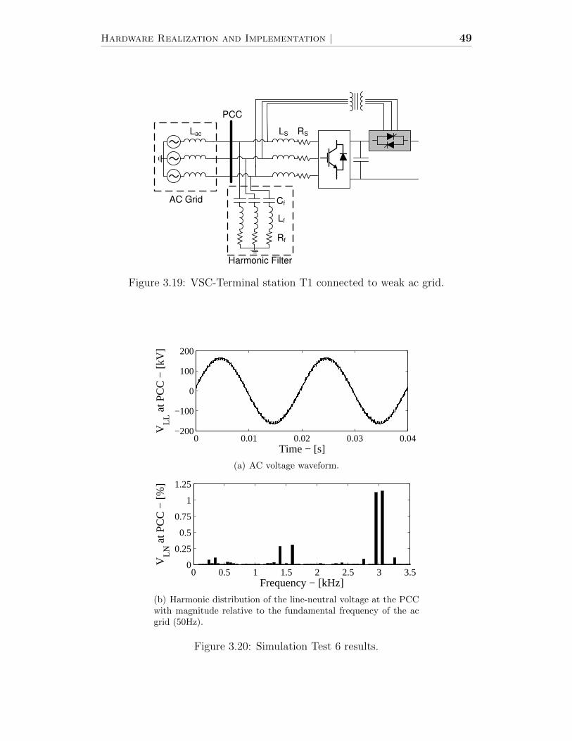
Hardware Realization and Implementation | 49
~~~
PCC
LS RSLac
Lf
Rf
Cf
Harmonic Filter
AC Grid
Figure 3.19: VSC-Terminal station T1 connected to weak ac grid.
0 0.01 0.02 0.03 0.04−200
−100
0
100
200
VLL
at P
CC
− [k
V]
Time − [s]
(a) AC voltage waveform.
0 0.5 1 1.5 2 2.5 3 3.50
0.25
0.5
0.75
1
1.25
VLN
at P
CC
− [%
]
Frequency − [kHz]
(b) Harmonic distribution of the line-neutral voltage at the PCCwith magnitude relative to the fundamental frequency of the acgrid (50Hz).
Figure 3.20: Simulation Test 6 results.

50 Chapter 3 | DC Power Flow Controller
3.6 Chapter Summary
This chapter has presented a dc power flow controller under the name of
“thyristor power flow controller”. The thyristor power flow controller consists
of two 6-pulse thyristor-bridges connected in a dual-converter configuration so
that it has 4-quadrant control. It benefits from being a small appendage of
a VSC-HVDC station which lifts it to the high voltage of the dc line. It also
takes advantage of the relatively small dc line resistance so that by inserting
only a small dc voltage a very much larger dc power is controlled. Its smallness
also means that its contribution to harmonic distortion is also small.
The thyristor power flow controller has been tested by simulations (PSCAD-
EMTDC software package) in a 3-terminal HVDC system. Tests include: step
power injection, loss of a terminal station as well as operation with weak ac
line. The results show that the thyristor power flow controller is fast and sta-
ble. Total Harmonic Distortion (THD) and individual harmonic requirements
are satisfied.
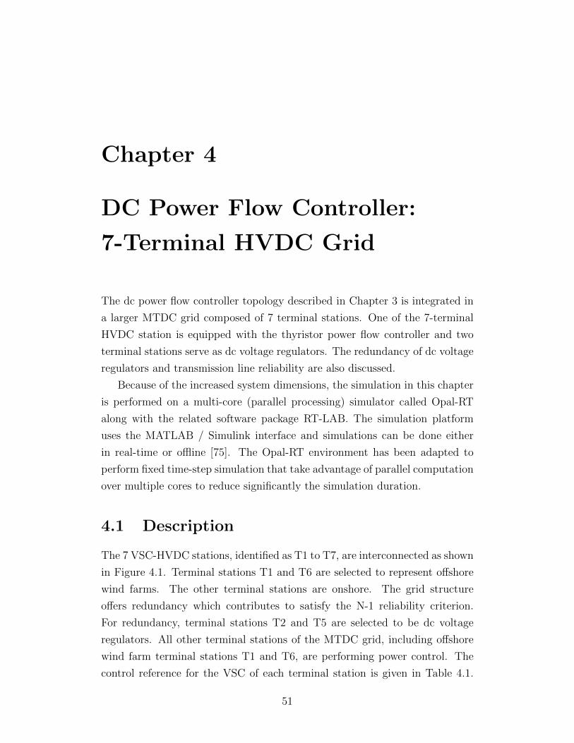
Chapter 4
DC Power Flow Controller:
7-Terminal HVDC Grid
The dc power flow controller topology described in Chapter 3 is integrated in
a larger MTDC grid composed of 7 terminal stations. One of the 7-terminal
HVDC station is equipped with the thyristor power flow controller and two
terminal stations serve as dc voltage regulators. The redundancy of dc voltage
regulators and transmission line reliability are also discussed.
Because of the increased system dimensions, the simulation in this chapter
is performed on a multi-core (parallel processing) simulator called Opal-RT
along with the related software package RT-LAB. The simulation platform
uses the MATLAB / Simulink interface and simulations can be done either
in real-time or offline [75]. The Opal-RT environment has been adapted to
perform fixed time-step simulation that take advantage of parallel computation
over multiple cores to reduce significantly the simulation duration.
4.1 Description
The 7 VSC-HVDC stations, identified as T1 to T7, are interconnected as shown
in Figure 4.1. Terminal stations T1 and T6 are selected to represent offshore
wind farms. The other terminal stations are onshore. The grid structure
offers redundancy which contributes to satisfy the N-1 reliability criterion.
For redundancy, terminal stations T2 and T5 are selected to be dc voltage
regulators. All other terminal stations of the MTDC grid, including offshore
wind farm terminal stations T1 and T6, are performing power control. The
control reference for the VSC of each terminal station is given in Table 4.1.
51
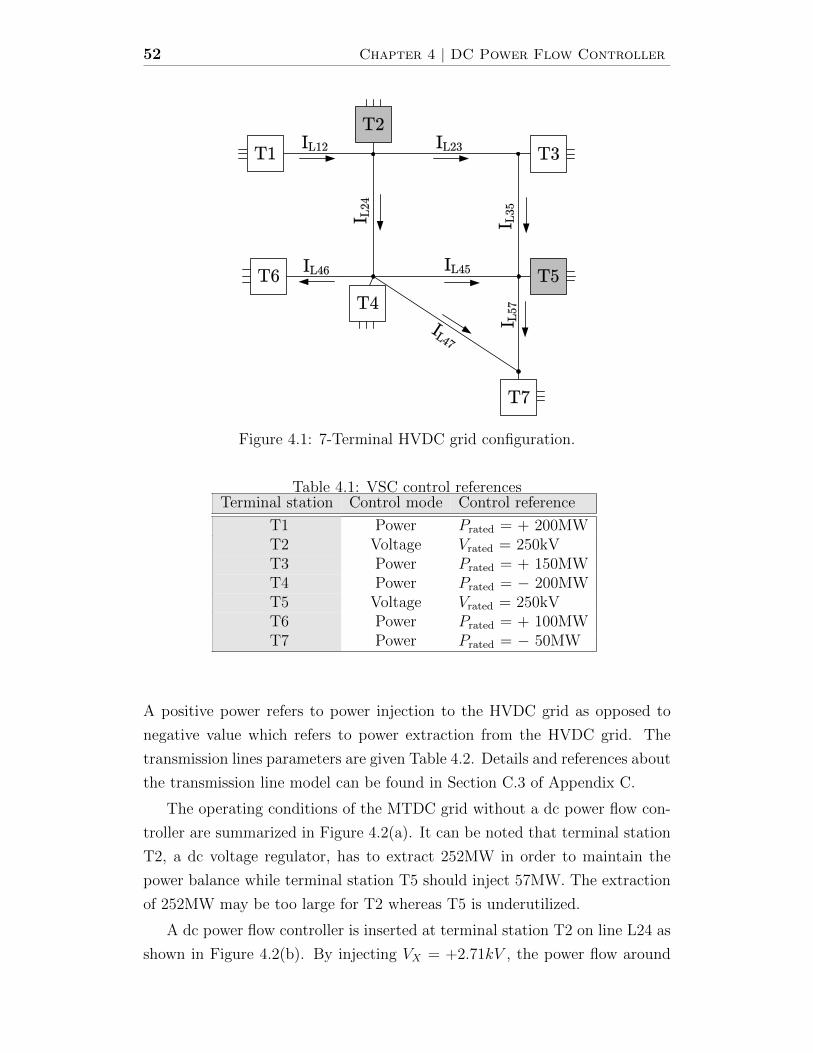
52 Chapter 4 | DC Power Flow Controller
T1
T6
T3
T5
T4
T7
T2
IL12 IL23
IL24
IL35
IL45IL46
IL57
IL47
Figure 4.1: 7-Terminal HVDC grid configuration.
Table 4.1: VSC control referencesTerminal station Control mode Control reference
T1 Power Prated = + 200MWT2 Voltage Vrated = 250kVT3 Power Prated = + 150MWT4 Power Prated = − 200MWT5 Voltage Vrated = 250kVT6 Power Prated = + 100MWT7 Power Prated = − 50MW
A positive power refers to power injection to the HVDC grid as opposed to
negative value which refers to power extraction from the HVDC grid. The
transmission lines parameters are given Table 4.2. Details and references about
the transmission line model can be found in Section C.3 of Appendix C.
The operating conditions of the MTDC grid without a dc power flow con-
troller are summarized in Figure 4.2(a). It can be noted that terminal station
T2, a dc voltage regulator, has to extract 252MW in order to maintain the
power balance while terminal station T5 should inject 57MW. The extraction
of 252MW may be too large for T2 whereas T5 is underutilized.
A dc power flow controller is inserted at terminal station T2 on line L24 as
shown in Figure 4.2(b). By injecting VX = +2.71kV , the power flow around

7-Terminal HVDC Grid | 53
Table 4.2: Transmission line parametersLines L12 L23 L24 L35 L45 L46 L47 L57
Distance [km] 413 248 207 331 83 207 289 165Resistance [Ω] 5 3 2.5 4 1 2.5 3.5 2Inductance [mH] 44 26 22 35 9 22 31 17
0.79kA 0.34kA
0.1kA
0.40kA 0.30kA
0.26kA
0.18kA
0.02kA
T2
250kV
-252MW
T4
-200MW
T1
+200MW
T6
+100MW
T3
+150MW
T5
250kV
+57MW
T7
-50MW
(a) without dc power flow controller.
0.79kA 0.34kA
0.93kA
0.40kA 0.39kA
0.26kA
0.06kA
0.14kA
T2
250kV
-50MW
T4
-200MW
T1
+200MW
T6
+100MW
VX
+2.7kV
T3
+150MW
T5
250kV
T7
-50MW
-146MW
(b) with power flow controller.
Figure 4.2: Normal operation of the 7-terminal HVDC grid
terminal station T2 is changed and the power extracted by terminal station
T2 is reduced from 252MW to 50MW. What was 252MW in T2 is now shifted
to T5 which now has to extract 146MW. The re-routing of dc power is evident
by comparing the transmission line currents in Figures 4.2(a) and 4.2(b). The
VSCs at terminal stations T2 and T5 continue to perform dc voltage regulator
at 250kV and it is VX of the dc power flow controller which diverts the power
flow. The other terminal stations are still performing power injection based
on their reference values.
4.2 Redundancy in DC Voltage Regulator
The presence of two dc voltage regulators, T2 and T5, makes the MTDC more
reliable in case of failure of one of the voltage reference terminal stations. For
example, the loss of terminal station T2 allows the MTDC grid to operate nor-
mally and steady-state currents are shown in Figure 4.3(a). For this scenario,
it has been assumed that the VSC as well as the dc power flow controller at
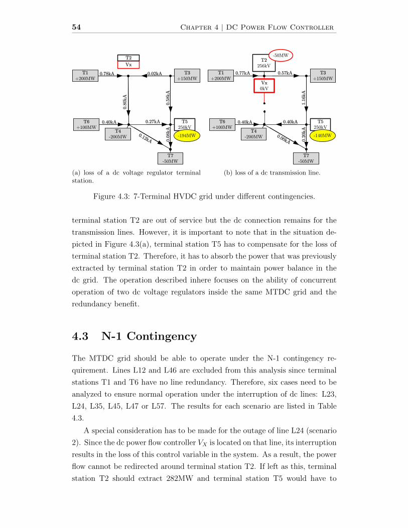
54 Chapter 4 | DC Power Flow Controller
0.78kA 0.02kA
0.80kA
0.40kA 0.27kA
0.58kA
0.08kA
0.12kA
T4
-200MW
T1
+200MW
T6
+100MW
T3
+150MW
T5
250kV
T7
-50MW
-194MW
Vx
T2
(a) loss of a dc voltage regulator terminalstation.
Vx
0kV
T2
256kV
-50MW
0.77kA 0.57kA
0.40kA 0.40kA
1.16kA
0.20kA
0.00kA
T4
-200MW
T1
+200MW
T6
+100MW
T3
+150MW
T5
250kV
T7
-50MW
-140MW
(b) loss of a dc transmission line.
Figure 4.3: 7-Terminal HVDC grid under different contingencies.
terminal station T2 are out of service but the dc connection remains for the
transmission lines. However, it is important to note that in the situation de-
picted in Figure 4.3(a), terminal station T5 has to compensate for the loss of
terminal station T2. Therefore, it has to absorb the power that was previously
extracted by terminal station T2 in order to maintain power balance in the
dc grid. The operation described inhere focuses on the ability of concurrent
operation of two dc voltage regulators inside the same MTDC grid and the
redundancy benefit.
4.3 N-1 Contingency
The MTDC grid should be able to operate under the N-1 contingency re-
quirement. Lines L12 and L46 are excluded from this analysis since terminal
stations T1 and T6 have no line redundancy. Therefore, six cases need to be
analyzed to ensure normal operation under the interruption of dc lines: L23,
L24, L35, L45, L47 or L57. The results for each scenario are listed in Table
4.3.
A special consideration has to be made for the outage of line L24 (scenario
2). Since the dc power flow controller VX is located on that line, its interruption
results in the loss of this control variable in the system. As a result, the power
flow cannot be redirected around terminal station T2. If left as this, terminal
station T2 should extract 282MW and terminal station T5 would have to

7-Terminal HVDC Grid | 55
Table 4.3: N-1 contingency scenariosScenario VX [kV] L23 L24 L35 L45 L47 L57
1 +1.56 OUT 0.59 0.59 0.10 0.09 0.112* OUT 0.57 OUT 1.16 -0.40 0.00 0.203 +3.56 -0.60 1.18 OUT 0.60 0.18 0.024 +4.85 -0.34 0.93 0.26 OUT 0.53 -0.335 +2.85 -0.34 0.93 0.26 0.53 OUT 0.206 +2.65 -0.34 0.93 0.26 0.33 0.20 OUT
*Terminal station T2 control changes to constant power control
inject 87MW. This is beyond the power rating of 50MW initially planned for
terminal station T2 converter. Suggested solutions are: i) the installation of
a second dc power flow controller on line L23 for redundancy or ii) a change
in the mode of operation of terminal station T2 under this circumstance only.
Terminal station T2 would change from dc voltage regulator to constant power
extraction of 50MW. The redundancy in the dc voltage regulator and the
flexibility of the terminal station control settings allow the MTDC grid to
operate in this manner as shown in Figure 4.3(b). This analysis confirms that
the MTDC under study is capable of operating in agreement with the N-1
criterion of a power system.
4.4 Simulation Results
Each terminal station is composed of a VSC model as shown in Figure 4.4(a).
In addition to the VSC, terminal station T2 has the thyristor power flow
controller based on the thyristor topology described in Chapter 3 and it is
shown in Figure 4.4(b). Complete details about the VSC model and their
controllers are given in Section C.5 of Appendix C.
The analysis of the results is divided into three segments. The first seg-
ment, ranging from t=0s to t=2s, is the steady-state operation of the MTDC
grid. It demonstrates the normal operation conditions shown in Figure 4.2(b).
Terminal station powers, voltages and transmission line currents are shown in
Figures 4.5(a), 4.5(b) and 4.6(a), respectively. Terminal stations T2 and T5
succeed to maintain their dc-side voltages at 250kV. All the other terminal sta-
tions regulate at their power reference values. The transmission line currents
are in agreement with the theoretical values shown in Figure 4.2(b).
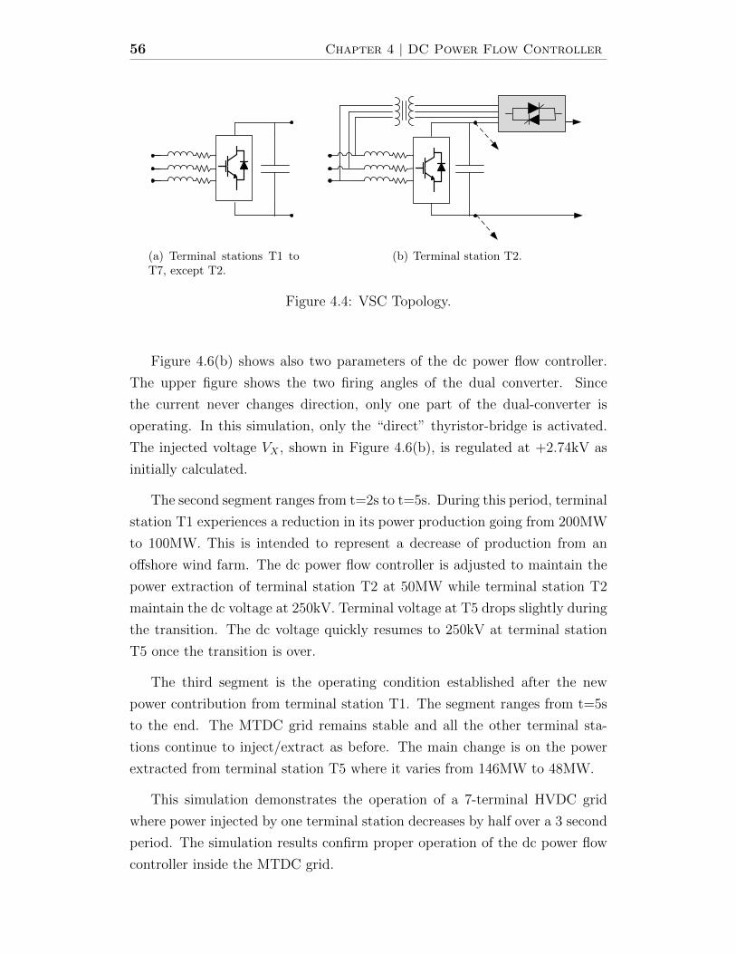
56 Chapter 4 | DC Power Flow Controller
(a) Terminal stations T1 toT7, except T2.
(b) Terminal station T2.
Figure 4.4: VSC Topology.
Figure 4.6(b) shows also two parameters of the dc power flow controller.
The upper figure shows the two firing angles of the dual converter. Since
the current never changes direction, only one part of the dual-converter is
operating. In this simulation, only the “direct” thyristor-bridge is activated.
The injected voltage VX , shown in Figure 4.6(b), is regulated at +2.74kV as
initially calculated.
The second segment ranges from t=2s to t=5s. During this period, terminal
station T1 experiences a reduction in its power production going from 200MW
to 100MW. This is intended to represent a decrease of production from an
offshore wind farm. The dc power flow controller is adjusted to maintain the
power extraction of terminal station T2 at 50MW while terminal station T2
maintain the dc voltage at 250kV. Terminal voltage at T5 drops slightly during
the transition. The dc voltage quickly resumes to 250kV at terminal station
T5 once the transition is over.
The third segment is the operating condition established after the new
power contribution from terminal station T1. The segment ranges from t=5s
to the end. The MTDC grid remains stable and all the other terminal sta-
tions continue to inject/extract as before. The main change is on the power
extracted from terminal station T5 where it varies from 146MW to 48MW.
This simulation demonstrates the operation of a 7-terminal HVDC grid
where power injected by one terminal station decreases by half over a 3 second
period. The simulation results confirm proper operation of the dc power flow
controller inside the MTDC grid.

7-Terminal HVDC Grid | 57
0 1 2 3 4 5 6 7 8−250
−200
−150
−100
−50
0
50
100
150
200
250
Pow
er a
t ter
min
al s
tatio
n −
[MW
]
Time − [s]
PT1
PT2
PT3
PT4
PT5
PT6
PT7
(a) Power injection/extraction.
1 2 3 4 5 6 7 8249.5
250
250.5
251
251.5
252
252.5
253
253.5
254
Ter
min
al v
olta
ge −
[kV
]Time − [s]
VT1
VT6
VT3
VT4
VT5 V
T2
VT7
(b) Terminal dc voltages.
Figure 4.5: 7-Terminal HVDC grid simulation results: power injec-tion/extraction and terminal dc voltages.
0 1 2 3 4 5 6 7 8−0.5
0
0.5
1
Tra
nsm
issi
on li
ne c
urre
nt −
[kA
]
Time − [s]
IL24
IL12
IL45
IL35
IL47
IL57
IL23
IL46
(a) Transmission line currents.
0 1 2 3 4 5 6 7 80
20
40
60
80
100
Firi
ng A
ngle
− [d
eg]
Time − [s]
αdir
αinv
0 1 2 3 4 5 6 7 81
1.5
2
2.5
3
VX
− [k
V]
Time − [s]
(b) DC power flow controller.
Figure 4.6: 7-Terminal HVDC grid simulation results: transmission line cur-rents and dc power flow controller.

58 Chapter 4 | DC Power Flow Controller
4.5 Chapter Summary
This chapter has presented a 7-terminal VSC-HVDC grid. It has been devel-
oped with an analysis on the dc voltage regulator redundancy as well as on
the N-1 contingency criterion. This 7-terminal HVDC grid with VSC models
has been simulated on a multi-core platform to show stable operation under
steady-state and dynamic condition.

Part II
Marx DC-DC Converter
59

60

Chapter 5
Marx DC-DC Converter:
Concept and Operation
A dc-dc converter serves the function of changing the output to input dc
voltage ratio. This chapter introduces the concept and the topology of the
Marx converter as a continuous dc-dc converter. The topology is described for
single-stage and cascaded-stage configurations. The operation is demonstrated
through simulation of a cascaded converter.
5.1 Single-Stage Marx Converter
5.1.1 Basic Marx Converter Operation
The topology of the proposed single-stage converter is shown in Figure 5.1.
The concept consists of charging capacitors in parallel and reconnecting them
in series. The input is a dc voltage source (VS) and the load is modeled by
a resistor (Rload). For purpose of illustration, the number of capacitors C1 is
M=3 to create a voltage amplification of 3. The switching components are
IGBTs and fast recovery diodes. The periodicity of operation is tsw second,
divided into two equal sub-periods of duration tsw/2 s.
In the first sub-period, the capacitors C1 are charged in parallel as illus-
trated in Figure 5.2(a). The charging currents flow through S1, D1, (DA, SA),
(DB, SB) and directly to the three capacitors connected between L1 and the
ground. In the second sub-period, the capacitors are connected in series to
create a high voltage, 3VS, as shown in Figure 5.2(b). This is initiated by
switching IGBTs SAA and SBB ON and SA and SB OFF.
61
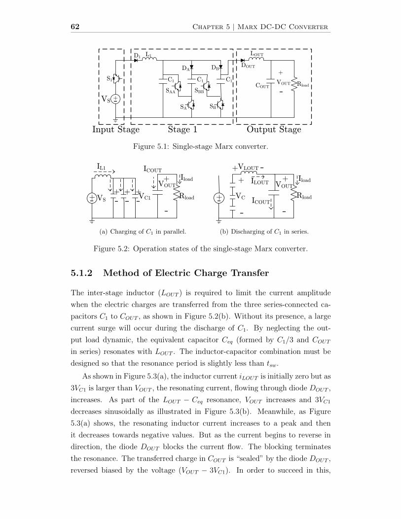
62 Chapter 5 | Marx DC-DC Converter
+
L1 LOUT
C1COUT Rload
+
VS
S1
D1
DA
SA
DOUT
VOUT
DB
SB
SBB
C1
SAA
C1
Output StageInput Stage Stage 1
Figure 5.1: Single-stage Marx converter.
+ Rload
+
VS+
VC1
IL1
IloadVOUT
ICOUT
+ +
(a) Charging of C1 in parallel.
+ Rload
+ ILOUTIload
VC
+VLOUT
ICOUT
+VOUT
(b) Discharging of C1 in series.
Figure 5.2: Operation states of the single-stage Marx converter.
5.1.2 Method of Electric Charge Transfer
The inter-stage inductor (LOUT ) is required to limit the current amplitude
when the electric charges are transferred from the three series-connected ca-
pacitors C1 to COUT , as shown in Figure 5.2(b). Without its presence, a large
current surge will occur during the discharge of C1. By neglecting the out-
put load dynamic, the equivalent capacitor Ceq (formed by C1/3 and COUT
in series) resonates with LOUT . The inductor-capacitor combination must be
designed so that the resonance period is slightly less than tsw.
As shown in Figure 5.3(a), the inductor current iLOUT is initially zero but as
3VC1 is larger than VOUT , the resonating current, flowing through diode DOUT ,
increases. As part of the LOUT − Ceq resonance, VOUT increases and 3VC1
decreases sinusoidally as illustrated in Figure 5.3(b). Meanwhile, as Figure
5.3(a) shows, the resonating inductor current increases to a peak and then
it decreases towards negative values. But as the current begins to reverse in
direction, the diode DOUT blocks the current flow. The blocking terminates
the resonance. The transferred charge in COUT is “sealed” by the diode DOUT ,
reversed biased by the voltage (VOUT − 3VC1). In order to succeed in this,

Concept and Operation | 63
Time
iLOUT
(tsw/2)
Curr
en
t
(a) Inductor current.
Time(tsw/2)
VOUT
3VC1Vo
ltag
e
(b) Capacitor and output voltages.
Figure 5.3: Voltage and current waveforms for the discharge from C1 in seriesto COUT . The voltage waveforms neglect the output load dynamic.
+
L1
COUT
Rload+
VS VOUTC1
LOUT
Stage 1 Output Stage
M capacitors
Stage N
M capacitors
Input Stage
LN
CN
Figure 5.4: Generalized Marx Converter with multiple stages (N) composed ofM capacitors per stage.
the inductor-capacitor combination must be designed so that the resonance
frequency is less than 1/tsw.
The repeated charging of C1 in parallel and discharging in series enables
the Marx converter to deliver power with a voltage gain of M=3 in the exam-
ple of Figures 5.1 and 5.2. The capacitor COUT serves as charge storage for
continuous delivery. It has to be large enough with respect to the switching
frequency, fsw = 1/tsw, so that the load current, Iload, has low ripples.
5.2 Multiple Stage Converter
5.2.1 Basic Structure of Cascaded Stages
Figure 5.4 shows N stages of the Marx converter connected in cascade. There
is a common grounding point for the input voltage source, the intermediate
stages and the load. The topology of every stage is identical but the sizes
of components are tailored to the current carrying capacity and the voltage
withstand required for the particular stage. The topology of the input stage

64 Chapter 5 | Marx DC-DC Converter
(n=0) and the output stage (n=N+1) is the same as in Figure 5.1.
The presentation is made simpler by specifying the number of stages to N=3
and the number of capacitors per stage to M=3. The overall dc voltage gain is
MN = 33 = 27. The voltage gain can easily generalize for different values of M
and N. For N=3 in Figure 5.4, the inter-stage inductances are L1, L2, L3, LOUT
and the capacitances of the 3 stages are C1, C2, C3. The resistances in the
inductors are neglected in the first instance so that the principles of the method
are more easily understood. The resistances are reinstated in the analysis in
the next chapter.
5.2.2 “Bucket Brigade” Electric Charge Transfers
The method of transferring the electric charge from the voltage source VS to
the load Rload, resembles the bucket brigade used in putting out fires. The
solid-state switches in the odd-numbered stages (n=1,3,...) follow the logic
notation S and the even-numbered stages (n=2,4,...) come under the logic
notation S. When S is 1, S is 0 and vice versa.
When S=1, the odd-numbered stages are getting charged by having their
capacitors connected in parallel. Their capacitors have been charged by the
series-connected capacitors of the previous even-numbered stages except for
stage 1 where it is from the input voltage source VS. This operation is illus-
trated in Figure 5.5(a). The charging currents flow through L1 and L3. There
is no current flowing in L2 and LOUT .
When S=0, the odd-numbered stages are discharging to the following even-
numbered stages by having their capacitor connected in series. The even-
numbered stages are configured with the capacitor connected in parallel. This
operation is illustrated in Figure 5.5(b). The charging currents flow through
L2 and LOUT . There is no current flowing in L1 and L3. In this example, the
output stage is on the sequence of an even-numbered stage (“stage 4”), which
means that it is getting charged when S=0.
The cascaded Marx converter operates by periodic alternate switching:
S=1, S=0, S=1, S=0,... The electric charges are transferred from the source,
VS, to stage n=1 and then to stage n=2... until they reach Rload, as in a bucket
brigade. The diodes which are in series with the inter-stage inductors ensure
unidirectional charge transfer.

Concept and Operation | 65
Stage 2 Stage 3
L3
C3
Stage 1
L1
C1 C2
RloadVS+ COUT
(a) Configuration when S=1.
VS
Stage 1 Stage 2 Stage 3
C1
L2
C2 C3
LOUT
RloadCOUT+
(b) Configuration when S=0.
Figure 5.5: The arrangements for the two sub-periods of equal duration tsw/2.
5.3 Analysis of Multi-Stage Marx Converter
For clarity in presentation, Figures 5.1, 5.2 and 5.5 have been drawn with M=3
capacitors for every stage. In order to derive formulas that will be generally
useful in design, this section and subsequent sections of this chapter return
to the algebraic M. It is assumed that periodic steady-state has already been
reached.
At this point, it is necessary to clarify the subscripts n and n+1 in the def-
inition of the equivalent capacitor symbol Ceq−n−n+1 which will be used. They
designate the equivalent capacitor formed by connecting M series capacitors
of size Cn (of the nth stage) to M parallel connected capacitors of size Cn+1
(of the (n+ 1)th stage) as shown in Figure 5.5.
For the multiple-stage system of Figure 5.4, the dc voltages increase as
by the geometric series. The output voltage gain of the nth stage is by the
relation:
VCn = MVC(n−1) (5.1)
So the output voltage is:
VOUT = MNVS (5.2)
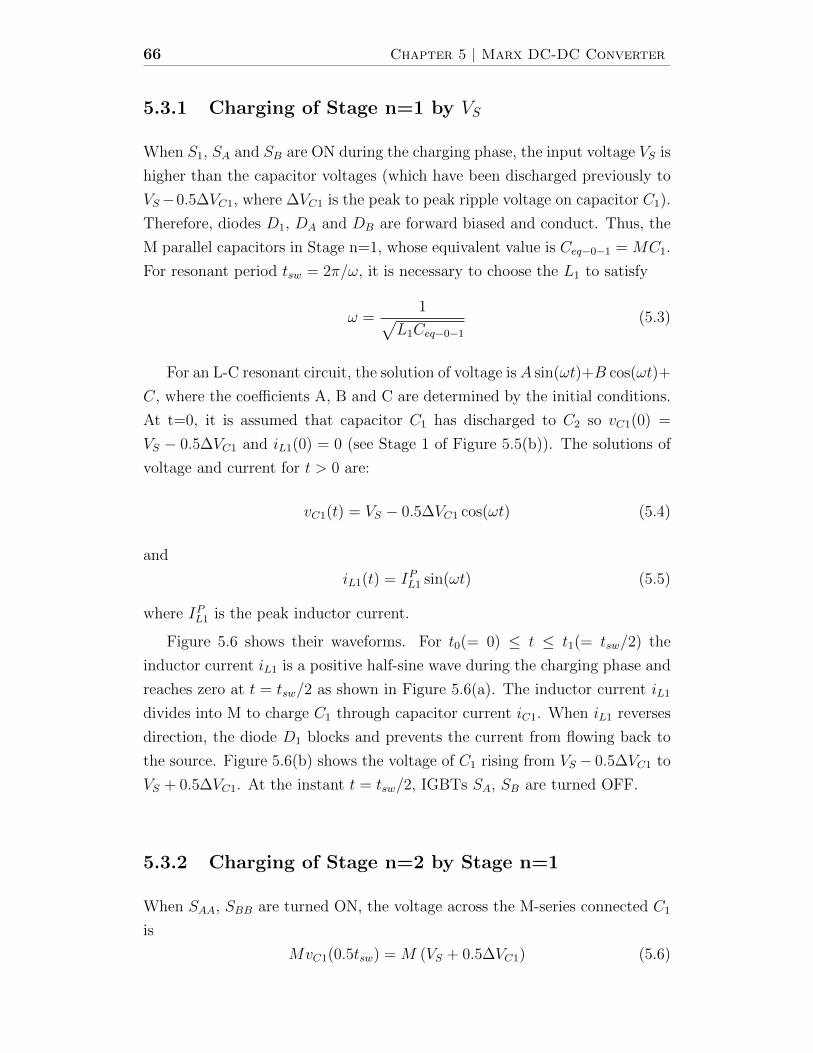
66 Chapter 5 | Marx DC-DC Converter
5.3.1 Charging of Stage n=1 by VS
When S1, SA and SB are ON during the charging phase, the input voltage VS is
higher than the capacitor voltages (which have been discharged previously to
VS−0.5∆VC1, where ∆VC1 is the peak to peak ripple voltage on capacitor C1).
Therefore, diodes D1, DA and DB are forward biased and conduct. Thus, the
M parallel capacitors in Stage n=1, whose equivalent value is Ceq−0−1 = MC1.
For resonant period tsw = 2π/ω, it is necessary to choose the L1 to satisfy
ω =1√
L1Ceq−0−1
(5.3)
For an L-C resonant circuit, the solution of voltage is A sin(ωt)+B cos(ωt)+
C, where the coefficients A, B and C are determined by the initial conditions.
At t=0, it is assumed that capacitor C1 has discharged to C2 so vC1(0) =
VS − 0.5∆VC1 and iL1(0) = 0 (see Stage 1 of Figure 5.5(b)). The solutions of
voltage and current for t > 0 are:
vC1(t) = VS − 0.5∆VC1 cos(ωt) (5.4)
and
iL1(t) = IPL1 sin(ωt) (5.5)
where IPL1 is the peak inductor current.
Figure 5.6 shows their waveforms. For t0(= 0) ≤ t ≤ t1(= tsw/2) the
inductor current iL1 is a positive half-sine wave during the charging phase and
reaches zero at t = tsw/2 as shown in Figure 5.6(a). The inductor current iL1
divides into M to charge C1 through capacitor current iC1. When iL1 reverses
direction, the diode D1 blocks and prevents the current from flowing back to
the source. Figure 5.6(b) shows the voltage of C1 rising from VS − 0.5∆VC1 to
VS + 0.5∆VC1. At the instant t = tsw/2, IGBTs SA, SB are turned OFF.
5.3.2 Charging of Stage n=2 by Stage n=1
When SAA, SBB are turned ON, the voltage across the M-series connected C1
is
MvC1(0.5tsw) = M (VS + 0.5∆VC1) (5.6)

Concept and Operation | 67
(tsw/2)
iL1
iC1
IL1P
IL2P iL2
t0 t1 t2
(tsw/2)
Current
Time
(a) Current.
(tsw/2) (tsw/2)
VC1
t0 t1 t2
VS
Voltage
Time
vC1
(b) Capacitor voltage.
Figure 5.6: Ideal resonant waveforms for the currents and voltages.
As illustrated in Figure 5.5(b), the M parallel connected capacitors C2 of Stage
2 are charged by the M series connected capacitors C1 of Stage 1. The equiv-
alent capacitance is:
Ceq−1−2 =(C1/M)(MC2)
C1/M +MC2
(5.7)
The inductance L2 is chosen so that the resonance frequency remains the same
as that for Equation (5.3); that is:
ω =1√
L2Ceq−1−2
(5.8)
Figures 5.6(a) and 5.6(b) show the waveforms of the currents iC1, iL2 and
of the voltage vC1. In Stage 2, for t1 ≤ t ≤ t2, the inductor current iL2 = −iC1
divides into M to charge C2. Because the charging current of C2 is reduced
by M, in order to maintain the relative voltage ripple (∆VC2/VC2) the same as
with (∆VC1/VC1) for capacitor C1, it is necessary to make C2 = C1/M2. By
doing so, the voltage ripple for capacitor C2 is:
∆VC2 = M∆VC1 (5.9)
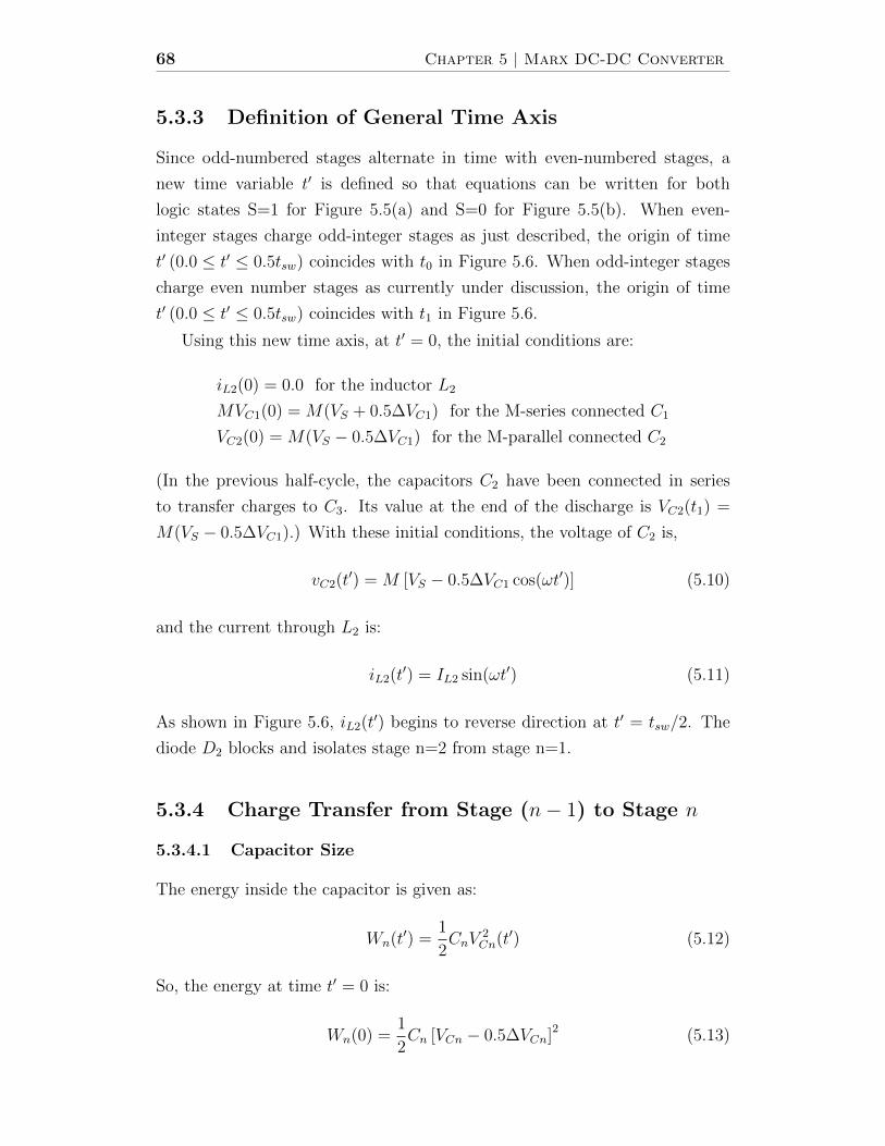
68 Chapter 5 | Marx DC-DC Converter
5.3.3 Definition of General Time Axis
Since odd-numbered stages alternate in time with even-numbered stages, a
new time variable t′ is defined so that equations can be written for both
logic states S=1 for Figure 5.5(a) and S=0 for Figure 5.5(b). When even-
integer stages charge odd-integer stages as just described, the origin of time
t′ (0.0 ≤ t′ ≤ 0.5tsw) coincides with t0 in Figure 5.6. When odd-integer stages
charge even number stages as currently under discussion, the origin of time
t′ (0.0 ≤ t′ ≤ 0.5tsw) coincides with t1 in Figure 5.6.
Using this new time axis, at t′ = 0, the initial conditions are:
iL2(0) = 0.0 for the inductor L2
MVC1(0) = M(VS + 0.5∆VC1) for the M-series connected C1
VC2(0) = M(VS − 0.5∆VC1) for the M-parallel connected C2
(In the previous half-cycle, the capacitors C2 have been connected in series
to transfer charges to C3. Its value at the end of the discharge is VC2(t1) =
M(VS − 0.5∆VC1).) With these initial conditions, the voltage of C2 is,
vC2(t′) = M [VS − 0.5∆VC1 cos(ωt′)] (5.10)
and the current through L2 is:
iL2(t′) = IL2 sin(ωt′) (5.11)
As shown in Figure 5.6, iL2(t′) begins to reverse direction at t′ = tsw/2. The
diode D2 blocks and isolates stage n=2 from stage n=1.
5.3.4 Charge Transfer from Stage (n− 1) to Stage n
5.3.4.1 Capacitor Size
The energy inside the capacitor is given as:
Wn(t′) =1
2CnV
2Cn(t′) (5.12)
So, the energy at time t′ = 0 is:
Wn(0) =1
2Cn [VCn − 0.5∆VCn]2 (5.13)
Concept and Operation | 69
Similarly, the energy at time t′ = tsw/2 is:
Wn(tsw/2) =1
2Cn [VCn + 0.5∆VCn]2 (5.14)
Therefore, the energy transferred in a given sub-period is calculated as:
∆Wn = Wn(tsw/2)−Wn(0) = CnVCn∆VCn (5.15)
Using Equation (5.15), the energy transferred for stage (n− 1) is:
∆Wn−1 = Cn−1VC(n−1)∆VC(n−1) (5.16)
By having the same relative capacitor voltage ripple between stages, Equation
(5.17) is obtained.∆VCnVCn
=∆VC(n−1)
VC(n−1)
(5.17)
Assuming conversation of energy, it is possible to equate Equations (5.15) and
(5.16). When it is combined with Equations (5.1) and (5.17), the capacitor
size is expressed as:
Cn =Cn−1
M2(5.18)
or in terms of C1:
Cn =C1
M2n−2(5.19)
The equivalent capacitance Ceq−n when charging capacitors of stage n with
capacitors of stage (n− 1) is:
Ceq−n =MCn−1Cn
Cn−1 +M2Cn(5.20)
substituting Equation (5.19) in Equation (5.20),
Ceq−n =1
2
C1
M2n−3(5.21)
5.3.4.2 Capacitor Voltage
The voltage across capacitor Cn is of the form:
vCn(t′) = Mn−1VS − 0.5∆VCn cos(ωt′) (5.22)

70 Chapter 5 | Marx DC-DC Converter
Dn
Stage n-1 Stage n
VCn-1
++
VCn
Figure 5.7: Configuration when stage (n− 1) is charging (parallel connection)and stage n is discharging (series connection).
where the capacitor peak to peak voltage ripple ∆VCn is
∆VCn = Mn−1∆VC1 (5.23)
which gives the general expression,
vCn(t′) = Mn−1 [VS − 0.5∆VC1 cos(ωt′)] (5.24)
Therefore at t′ = 0,
vCn(0) = Mn−1 [VS − 0.5∆VC1] (5.25)
and at t′ = 0.5tsw ,
vCn(0.5tsw) = Mn−1 [VS + 0.5∆VC1] (5.26)
An additional requirement has to be set regarding the allowed capacitor
voltage ripple. Figure 5.7 shows the configuration of the converter when stage
(n − 1) is charging (parallel connection) and stage n is discharging (series
connection). It is important that diode Dn remains reverse biased and it is
done by ensuring that VC(n−1) < VCn. The critical instant occurs when stage
(n− 1) is at its peak voltage ripple and stage n is at its lowest voltage ripple.
The relationship is shown in Equation (5.27) and it leads to a limit on the
capacitor voltage ripple.
Mn−2VS +∆VC(n−1)
2< Mn−1VS −
∆VCn2
(5.27)
Concept and Operation | 71
For the same relative capacitor voltage ripple, Equation (5.23) is inserted in
Equation (5.27) to obtain the requirements in terms of ∆VC1:
∆VC1
2<M − 1
M + 1VS (5.28)
The closer boundary occurs when M = 2 and the capacitor voltage ripple
should not exceed ±33% of the input voltage VS.
5.3.4.3 Capacitor Current
Applying CndvCn(t)dt
and substituting Equation (5.19), the discharging current
of Cn is:
iCn(t′) =0.5∆VC1ωC1 sin(ωt′)
Mn−1(5.29)
It is also the current of inductor Ln+1 for the sub-period when stage (n+ 1) is
charged. i.e. iLn+1(t′) = −iCn(t′) for tsw/2 < t′ < tsw.
5.3.4.4 Inductor Size
Generalizing from Equation (5.8) and applying Equation (5.21), in order to
ensure identical resonant periods, the inductance Ln+1 between stage n and
stage (n+ 1) is:
Ln+1 =2M2n−1
C1
(tsw2π
)2
(5.30)
5.3.5 Power Delivered
Substituting Equations (5.24) and (5.29), the power delivered by the M series-
connected Cn is:
pn(t′) = [MvCn(t′)] iCn(t′) = M
[VS −
∆VC1
2cos(ωt′)
] [∆VC1
2ωC1 sin(ωt′)
](5.31)
As the formula of pn(t′) in Equation (5.31) is independent of n, this shows that
by sizing the capacitors and the inductances according to Equations (5.19) and
(5.30) respectively, the transfer of power through all the converter stages are
identical. Integrating Equation (5.31) in the half-period, 0.5tsw, and taking
the average for the complete switching cycle:
Pn =1
tswMVSC1∆VC1 (5.32)
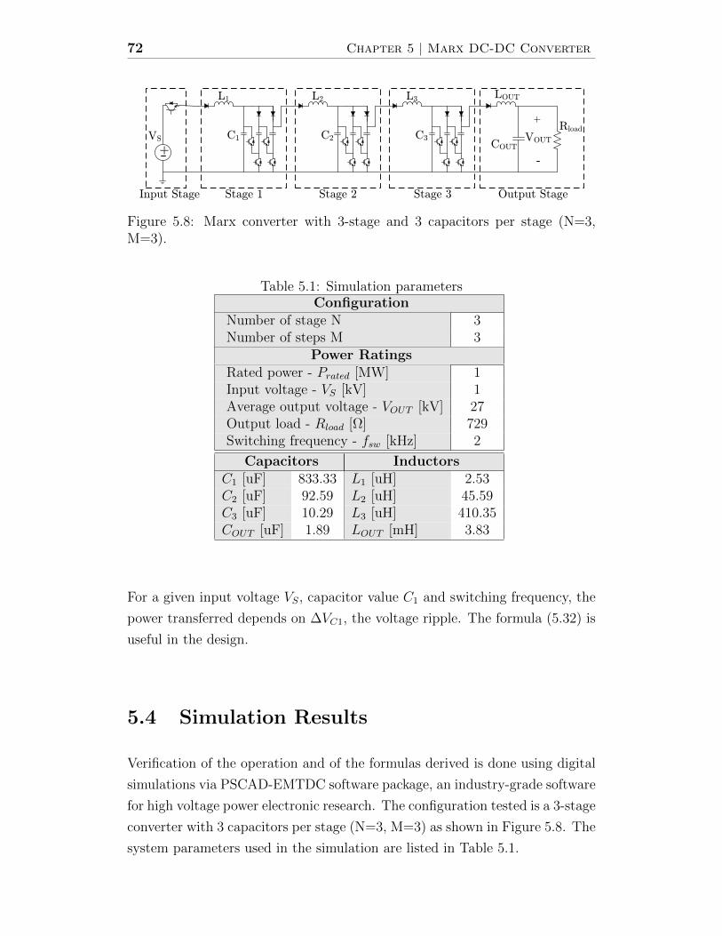
72 Chapter 5 | Marx DC-DC Converter
+
L1
COUT
Rload+
VS VOUTC1
LOUT
Stage 1 Output StageInput Stage
L2
C2
Stage 2
L3
C3
Stage 3
Figure 5.8: Marx converter with 3-stage and 3 capacitors per stage (N=3,M=3).
Table 5.1: Simulation parametersConfiguration
Number of stage N 3Number of steps M 3
Power RatingsRated power - Prated [MW] 1Input voltage - VS [kV] 1Average output voltage - VOUT [kV] 27Output load - Rload [Ω] 729Switching frequency - fsw [kHz] 2
Capacitors InductorsC1 [uF] 833.33 L1 [uH] 2.53C2 [uF] 92.59 L2 [uH] 45.59C3 [uF] 10.29 L3 [uH] 410.35COUT [uF] 1.89 LOUT [mH] 3.83
For a given input voltage VS, capacitor value C1 and switching frequency, the
power transferred depends on ∆VC1, the voltage ripple. The formula (5.32) is
useful in the design.
5.4 Simulation Results
Verification of the operation and of the formulas derived is done using digital
simulations via PSCAD-EMTDC software package, an industry-grade software
for high voltage power electronic research. The configuration tested is a 3-stage
converter with 3 capacitors per stage (N=3, M=3) as shown in Figure 5.8. The
system parameters used in the simulation are listed in Table 5.1.
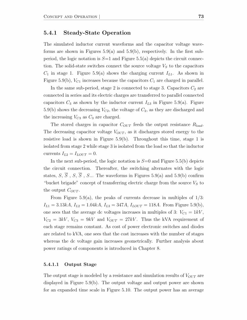
Concept and Operation | 73
5.4.1 Steady-State Operation
The simulated inductor current waveforms and the capacitor voltage wave-
forms are shown in Figures 5.9(a) and 5.9(b), respectively. In the first sub-
period, the logic notation is S=1 and Figure 5.5(a) depicts the circuit connec-
tion. The solid-state switches connect the source voltage VS to the capacitors
C1 in stage 1. Figure 5.9(a) shows the charging current IL1. As shown in
Figure 5.9(b), VC1 increases because the capacitors C1 are charged in parallel.
In the same sub-period, stage 2 is connected to stage 3. Capacitors C2 are
connected in series and its electric charges are transferred to parallel connected
capacitors C3 as shown by the inductor current IL3 in Figure 5.9(a). Figure
5.9(b) shows the decreasing VC2, the voltage of C2, as they are discharged and
the increasing VC3 as C3 are charged.
The stored charges in capacitor COUT feeds the output resistance Rload.
The decreasing capacitor voltage VOUT , as it discharges stored energy to the
resistive load is shown in Figure 5.9(b). Throughout this time, stage 1 is
isolated from stage 2 while stage 3 is isolated from the load so that the inductor
currents IL2 = ILOUT = 0.
In the next sub-period, the logic notation is S=0 and Figure 5.5(b) depicts
the circuit connection. Thereafter, the switching alternates with the logic
states, S, S , S, S , S... The waveforms in Figures 5.9(a) and 5.9(b) confirm
“bucket brigade” concept of transferring electric charge from the source VS to
the output COUT .
From Figure 5.9(a), the peaks of currents decrease in multiples of 1/3:
IL1 = 3.13kA, IL2 = 1.04kA, IL3 = 347A, ILOUT = 118A. From Figure 5.9(b),
one sees that the average dc voltages increases in multiples of 3: VC1 = 1kV ,
VC2 = 3kV , VC3 = 9kV and VOUT = 27kV . Thus the kVA requirement of
each stage remains constant. As cost of power electronic switches and diodes
are related to kVA, one sees that the cost increases with the number of stages
whereas the dc voltage gain increases geometrically. Further analysis about
power ratings of components is introduced in Chapter 8.
5.4.1.1 Output Stage
The output stage is modeled by a resistance and simulation results of VOUT are
displayed in Figure 5.9(b). The output voltage and output power are shown
for an expanded time scale in Figure 5.10. The output power has an average

74 Chapter 5 | Marx DC-DC Converter
0 0.1 0.2 0.3 0.4 0.5 0.6 0.7 0.8 0.9 1 1.1 1.20123
I L1 −
[kA
]0 0.1 0.2 0.3 0.4 0.5 0.6 0.7 0.8 0.9 1 1.1 1.2
0
0.5
1
I L2 −
[kA
]
0 0.1 0.2 0.3 0.4 0.5 0.6 0.7 0.8 0.9 1 1.1 1.20
200
400I L3
− [A
]
0 0.1 0.2 0.3 0.4 0.5 0.6 0.7 0.8 0.9 1 1.1 1.20
50100150
I LOU
T −
[A]
0 0.1 0.2 0.3 0.4 0.5 0.6 0.7 0.8 0.9 1 1.1 1.2−0.5
00.5
11.5
S
time − [ms]
(a) Inductor currents.
0 0.1 0.2 0.3 0.4 0.5 0.6 0.7 0.8 0.9 1 1.1 1.2
0.9
1
1.1
VC
1 − [k
V]
0 0.1 0.2 0.3 0.4 0.5 0.6 0.7 0.8 0.9 1 1.1 1.22.62.8
33.23.4
VC
2 − [k
V]
0 0.1 0.2 0.3 0.4 0.5 0.6 0.7 0.8 0.9 1 1.1 1.28
9
10
VC
3 − [k
V]
0 0.1 0.2 0.3 0.4 0.5 0.6 0.7 0.8 0.9 1 1.1 1.2
25
30
VO
UT −
[kV
]
0 0.1 0.2 0.3 0.4 0.5 0.6 0.7 0.8 0.9 1 1.1 1.2−0.5
00.5
11.5
S
time − [ms]
(b) Capacitor voltages.
Figure 5.9: Simulation results in the two sub-periods S=1 and S=0.

Concept and Operation | 75
0 2 4 6 8 10 12 14 16 18 200
10
20
30
VO
UT −
[kV
]
0 2 4 6 8 10 12 14 16 18 200
0.5
1P O
UT −
[MW
]
time − [ms]
Figure 5.10: Simulation results showing ripples on the output voltage andoutput power. The ripples are associated with alternate switching states ofthe converter.
Table 5.2: Design values and simulation resultsAverage voltage Voltage ripple
Design Simulation Design SimulationVC1 [kV] 1 1.00 ∆VC1 [kV] 0.2 0.20VC2 [kV] 3 2.99 ∆VC2 [kV] 0.6 0.60VC3 [kV] 9 8.98 ∆VC3 [kV] 1.8 1.79VCOUT [kV] 27 26.82 ∆VCOUT [kV] - 5.39
of 0.99MW, close to the designed 1MW power rating. The size of ripples can
be reduced by increasing COUT .
Table 5.2 lists under the column labelled “Design” the values computed
from the analytical solution. By their side are the simulated values. They
show agreement to within 0.7% in accuracy. The discrepancy is mainly due
to small resistances of the IGBT switches which have been omitted in the
analytical formulas but included in the simulation.
5.4.2 Transient Operation
In evaluating the transient response characteristics, two simulation runs have
been performed: (i) step-change on load side; (ii) step-change on source side.

76 Chapter 5 | Marx DC-DC Converter
0 5 10 15 20 25 30 35 400
2
4
I L1 −
[kA
]
0 5 10 15 20 25 30 35 40
25
30
VO
UT −
[kV
]
0 5 10 15 20 25 30 35 40640660680700720740
RLO
AD
− [
Ω ]
time − [ms]
Figure 5.11: Simulation results for inductor L1 current and output voltageVOUT for a step-change in load.
5.4.2.1 Step-Change on Load Side
A 10% step-change in the load is simulated by changing Rload from 729 ohms
to 656 ohms. The response is recorded in Figure 5.11. As to the load voltage,
the average output voltage remains at 26.78kV which is consistent with the
unchanged input voltage multiplied by a gain of MN = 27. The ripple ∆VOUT
has an increase of 11%, from 5.39kV to 6.00kV. This result is in agreement
with the formula derived in Equation (5.32).
The step change does not generate a large transient in the current IL1, the
current in inductor L1. The transient appears only at the third cycle after
the change because it takes a number of sub-periods for the step-change to
propagate upstream to inductor L1. The settling time is about 15ms.
5.4.2.2 Step-Change at Input Side
The step change test on the input side consists of decreasing VS from 1kV
to 0.9kV. As shown in Figure 5.12, initially the average of VOUT is 27kV and
settles to an average of 24kV. Both averages are consistent with the theoretical
amplification ratio of 27. It takes about 30ms for the transients to disappear.
The initial non-conduction periods of IL1 suggest that the voltages across
C2 have been higher than the voltages of series connected C1 so that the diode
D2 has been reverse biased. After few cycles, the voltages across capacitors
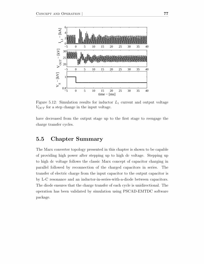
Concept and Operation | 77
−5 0 5 10 15 20 25 30 35 400
2
4
6
I L1 −
[kA
]
−5 0 5 10 15 20 25 30 35 40
20
25
30
VO
UT −
[kV
]
−5 0 5 10 15 20 25 30 35 400.8
1
VS −
[kV
]
time − [ms]
Figure 5.12: Simulation results for inductor L1 current and output voltageVOUT for a step change in the input voltage.
have decreased from the output stage up to the first stage to reengage the
charge transfer cycles.
5.5 Chapter Summary
The Marx converter topology presented in this chapter is shown to be capable
of providing high power after stepping up to high dc voltage. Stepping up
to high dc voltage follows the classic Marx concept of capacitor charging in
parallel followed by reconnection of the charged capacitors in series. The
transfer of electric charge from the input capacitor to the output capacitor is
by L-C resonance and an inductor-in-series-with-a-diode between capacitors.
The diode ensures that the charge transfer of each cycle is unidirectional. The
operation has been validated by simulation using PSCAD-EMTDC software
package.

78 Chapter 5 | Marx DC-DC Converter

Chapter 6
Marx DC-DC Converter:
Converter Design Guidelines
This chapter presents design guidelines for the presented Marx converter. The
analysis is intended to develop tools to select adequate inductor and capacitor
values depending on design requirements such as voltage ripples. The analysis
includes loss resistances associated with switches and passive components as
well as turn-off margin for switching events.
At the end of the chapter, the design of a 5kW converter is done. This 5kW
converter design will be used for the construction of the prototype presented
in the following chapter.
6.1 Initial Configuration
This section will go through the design steps of a converter with N-stages
and M-capacitors per stage as shown in Figure 6.1. The analysis assumes the
converter is in steady-state.
The switching frequency is fsw, therefore, a switching period of tsw(=
1/fsw). Each sub-period is of duration tsw/2. A turn-off margin, also called
dead-time, can be introduced in the design to ensure that the resonance is
terminated before the next switching event occurs. As soon as the inductor
current reaches zero, the series diode is reversed biased which creates the dead-
time. It is shown in Figure 6.2 and the dead-time period is identified as tdead.
The period used in the resonance calculation from the L-C parameters is tres
79
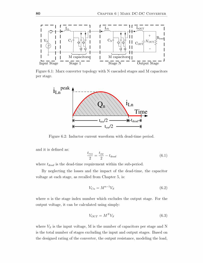
80 Chapter 6 | Marx DC-DC Converter
+
L1
COUT
Rload+
VS VOUTC1
LOUT
Stage 1 Output Stage
M capacitors
Stage N
M capacitors
Input Stage
LN
CN
Figure 6.1: Marx converter topology with N cascaded stages and M capacitorsper stage.
tsw/2
iLn
Time
tres/2 tdead
iLnpeak
Qn
Figure 6.2: Inductor current waveform with dead-time period.
and it is defined as:tres2
=tsw2− tdead (6.1)
where tdead is the dead-time requirement within the sub-period.
By neglecting the losses and the impact of the dead-time, the capacitor
voltage at each stage, as recalled from Chapter 5, is:
VCn = Mn−1VS (6.2)
where n is the stage index number which excludes the output stage. For the
output voltage, it can be calculated using simply:
VOUT = MNVS (6.3)
where VS is the input voltage, M is the number of capacitors per stage and N
is the total number of stages excluding the input and output stages. Based on
the designed rating of the converter, the output resistance, modeling the load,

Converter Design Guidelines | 81
is:
Rload =V 2OUT
Prated(6.4)
where VOUT is the average output voltage and Prated is the rated power of the
converter.
6.2 Capacitor Sizing
The amount of charge required by the load is used in the evaluation of the
capacitor sizing. The amount of charge in a complete switching period tsw at
the load is:
Qload =VOUTRload
tsw (6.5)
By combining Equations (6.3) and (6.4), Equation (6.5) can be rewritten as:
Qload =PratedMNVS
tsw (6.6)
6.2.1 Stage 1 to N
The first step consists of determining the capacitor value based on the desired
capacitor voltage ripple. The voltage ripple for capacitor at each stage is given
as:
∆VCn =Qn
MCn(6.7)
where n is the stage index number, Qn is the amount of charge transferred
for that stage and ∆VCn is the peak to peak voltage ripple in volts. The
relationship between Qn and Qload is:
Qn = MN−n+1Qload (6.8)
By using Qload and the voltage ripple, the capacitance at stage n can be cal-
culated by using:
Cn =Qload
∆VCnMN−n (6.9)
6.2.2 Output Stage
The results obtained from Equation (6.9) are not accurate for the output
stage. It can be explained by looking at the output capacitor voltage waveform
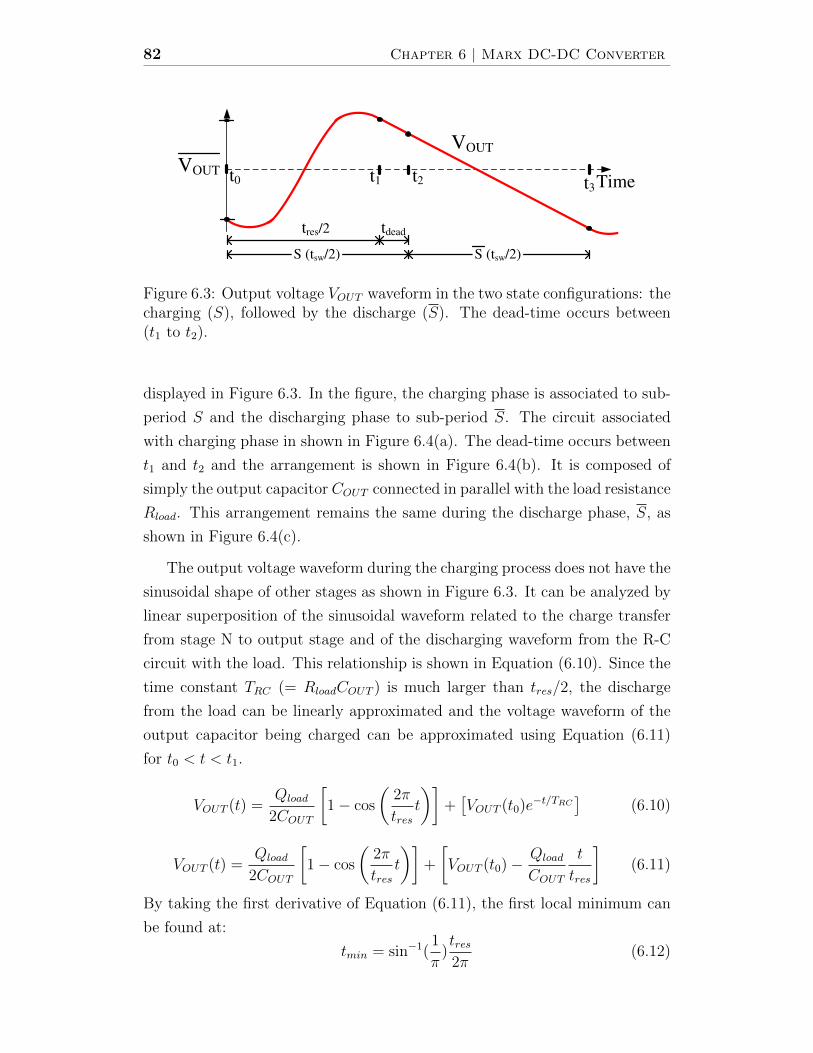
82 Chapter 6 | Marx DC-DC Converter
VOUT
t0 t1 t3Time
S (tsw/2)
tres/2 tdead
t2
S (tsw/2)
VOUT
Figure 6.3: Output voltage VOUT waveform in the two state configurations: thecharging (S), followed by the discharge (S). The dead-time occurs between(t1 to t2).
displayed in Figure 6.3. In the figure, the charging phase is associated to sub-
period S and the discharging phase to sub-period S. The circuit associated
with charging phase in shown in Figure 6.4(a). The dead-time occurs between
t1 and t2 and the arrangement is shown in Figure 6.4(b). It is composed of
simply the output capacitor COUT connected in parallel with the load resistance
Rload. This arrangement remains the same during the discharge phase, S, as
shown in Figure 6.4(c).
The output voltage waveform during the charging process does not have the
sinusoidal shape of other stages as shown in Figure 6.3. It can be analyzed by
linear superposition of the sinusoidal waveform related to the charge transfer
from stage N to output stage and of the discharging waveform from the R-C
circuit with the load. This relationship is shown in Equation (6.10). Since the
time constant TRC (= RloadCOUT ) is much larger than tres/2, the discharge
from the load can be linearly approximated and the voltage waveform of the
output capacitor being charged can be approximated using Equation (6.11)
for t0 < t < t1.
VOUT (t) =Qload
2COUT
[1− cos
(2π
trest
)]+[VOUT (t0)e−t/TRC
](6.10)
VOUT (t) =Qload
2COUT
[1− cos
(2π
trest
)]+
[VOUT (t0)− Qload
COUT
t
tres
](6.11)
By taking the first derivative of Equation (6.11), the first local minimum can
be found at:
tmin = sin−1(1
π)tres2π
(6.12)
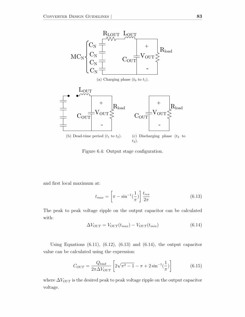
Converter Design Guidelines | 83
COUT
Rload+
VOUT
LOUT
MCN
CN
CN
CN
CN
RLOUT
(a) Charging phase (t0 to t1).
COUT
Rload+
VOUT
LOUT
(b) Dead-time period (t1 to t2).
COUT
Rload+
VOUT
(c) Discharging phase (t2 tot3).
Figure 6.4: Output stage configuration.
and first local maximum at:
tmax =
[π − sin−1(
1
π)
]tres2π
(6.13)
The peak to peak voltage ripple on the output capacitor can be calculated
with:
∆VOUT = VOUT (tmax)− VOUT (tmin) (6.14)
Using Equations (6.11), (6.12), (6.13) and (6.14), the output capacitor
value can be calculated using the expression:
COUT =Qload
2π∆VOUT
[2√π2 − 1− π + 2 sin−1(
1
π)
](6.15)
where ∆VOUT is the desired peak to peak voltage ripple on the output capacitor
voltage.
84 Chapter 6 | Marx DC-DC Converter
6.3 Inductor Sizing
The inductor is tailored such that the resonance in all configuration states
S and S is tres/2. It is important to note that, unlike the capacitors, each
inductor is used only during one sub-period, S or S. The equations are derived
based on the L-C configuration for each state. A resistance, labelled RLn, in
series with the inductor is included in the analysis. It is intended to model
various resistances present in the system including inductor, IGBT, diode and
wire losses.
6.3.1 Stage 1 to N
For stage 1 to N, the circuit equivalent model is simply composed of an equiv-
alent capacitance, the inductance and a resistance. This resistance introduces
a damping factor ζ in the system [76, 77]. More specifically, the resonance
frequency can be calculated using:
ωres = ω0
√1− ζ2 (6.16)
where ω0 is the undamped natural frequency calculated by,
ω0 =1√
LnCeq−n(6.17)
where Ln is the inductor and Ceq−n is the equivalent capacitance of the state
configuration. The damping factor ζ is calculated using:
ζ =RLn
2
√Ceq−nLn
(6.18)
where RLn is the loss resistance.
Using Equation (6.16) along with Equations (6.17) and (6.18), the inductor
for stage n can be calculated using:
Ln =1
8π2
t2resCeq−n
1 +
√1−
(2π
tresCeq−nRLn
)2 (6.19)
where the equivalent capacitor for the stage 1 is:
Ceq−1 = MC1 (6.20)

Converter Design Guidelines | 85
and for stages 2 to N, it is:
Ceq−n =MCn−1Cn
Cn−1 +M2Cn(6.21)
6.3.2 Output Stage
Mathematical complication arises for the computation of the output inductor
LOUT because the output load is modeled by a resistance Rload. By using
Figure 6.3, the output stage is charged from t0 to t1. The electric charge in
the series connected capacitors CN are transferred through inductance LOUT
to capacitor COUT which is connected in parallel to the load resistance Rload.
The circuit is shown in Figure 6.4(a).
In order to size the output inductor, recursive numerical computation is
used to solve this third order system. By using linear state-space equations,
the state configuration can be written in the form:
d
dtx(t) = [A]x(t) (6.22)
where x(t) = [iLOUT VCN VOUT ]T and [A] is a 3x3 time-invariant matrix
obtained from the three linear ordinary differential equations associated with
the state configuration S from t0 to t1. They are given in Equations (6.23),
(6.24) and (6.25).
d
dtiLOUT =
1
LOUT−iLOUTRLOUT +MVCN − VOUT (6.23)
d
dtVCN =
1
CN−iLOUT (6.24)
d
dtVOUT =
1
COUT
iLOUT −
VOUTRload
(6.25)
Therefore, matrix [A] is given as:
[A] =
−RLOUT
LOUT
MLOUT
− 1LOUT
− 1CN
0 01
COUT0 − 1
RloadCOUT
(6.26)
86 Chapter 6 | Marx DC-DC Converter
The solution for initial states, x(t0), is:
x(t) = e[A](t)x(t0) (6.27)
Using Figure 6.3 as guide, the state configuration S corresponds to (t0 ≤t ≤ t2). VOUT (t) has discharged and takes a value VOUT (t0) at the beginning
of the sub-period. The diode has blocked previously and, therefore, inductor
current iLOUT (t0) = 0.0. The capacitors CN have previously been charged in
parallel to(MN−1VS + 0.5∆VCN
)by stage N-1. Therefore, the initial state
vector is:
x(t0) =
0.0
MN−1VS + ∆VCN
2
VOUT (t0)
(6.28)
The initial conditions of iLOUT and VCN are known but the value of VOUT (t0)
is unknown. Its value is required in order to compute a precise value of LOUT .
At time t = t1, the voltage of COUT has been recharged to VOUT (t1) and
the diode stops conducting. The voltage for one series connected capacitor CN
has fallen to MN−1VS − 0.5∆VCN . It is desirable that current iLOUT (t1) = 0.0.
The state vector x at t1 is:
x(t1) =
0.0
MN−1VS − ∆VCN
2
VOUT (t1)
(6.29)
The relationship between VOUT (t1) and VOUT (t0) is made using remainder
of state configuration S (dead-time period) and the second state configuration
S where there is only the output capacitor and the load. The previously
charged capacitor COUT is being discharged by the load resistance Rload. The
well known solutions of R-C circuit in parallel are:
VOUT (t) = VOUT (t1)e−t
TRC (6.30)
where the time constant TRC = RloadCOUT and (t1 ≤ t ≤ t3). The exponen-
tially decaying output voltage VOUT (t) resembles a straight line in Figure 6.3
for time (t1 ≤ t ≤ t3). From periodicity, VOUT (t3) = VOUT (t0), and using
Equation (6.30) for a duration of t3 − t1 = tdead + 0.5tsw, Equation (6.31) is

Converter Design Guidelines | 87
obtained.
VOUT (t3) = VOUT (t0) = VOUT (t1)e− tdead+0.5tsw
TRC (6.31)
By using Equation (6.27), the solution for the charging phase from t0 to t1 is:
x(t1) = e[A](0.5tres)x(t0) (6.32)
By combining Equations (6.28), (6.29), (6.31) and (6.32), it gives:0.0
MN−1VS − ∆VCN
2
VOUT (t0)etdead+0.5tsw
TRC
= e[A](0.5tres)
0.0
MN−1VS + ∆VCN
2
VOUT (t0)
(6.33)
The matrix e[A](0.5tres) is a 3x3 matrix of 9 constant real numbers which are
evaluated using MATLAB. Equation (6.33) yields a linear algebraic system
of three equations where the unknown VOUT (t0) can be found. By defining
Γ = e[A](0.5tres), VOUT (t0) is calculated as:
VOUT (t0) =Γ(3,2)
(MN−1VS + ∆VCN
2
)e
tdead+0.5tswTRC − Γ(3,3)
(6.34)
where Γ(i,j) is the element at location (i,j) in the matrix Γ.
The iterative design steps are:
1. Construct matrix [A], Equation (6.26), for a selected LOUT value.
2. Compute VOUT (t0) using Equation (6.34) and use it to create the state
vector x(t0) with Equation (6.28).
3. Calculate x(t1) using Equation (6.32) and x(t0) from step 2.
The inductor current iLOUT should be zero at t1. Thus, the value of LOUT is
refined and iterative computations are done until the requirement is met.
6.4 Capacitor Voltage and Inductor Current
6.4.1 Capacitor Voltage
The capacitor sizing has been selected based on the approximation of the
voltage with neglecting the voltage drop associated with the resistance RLn

88 Chapter 6 | Marx DC-DC Converter
and the dead-time impact. The approach described in Section 6.2 is adequate
to select the capacitor values and then in Section 6.3 the inductor values are
calculated to create the adequate resonance period. However, it is possible to
refine the calculations to get an accurate value of the capacitor voltages and
the peak inductor current values.
The waveform for the inductor current is shown in Figure 6.2. It has a
sinusoidal shape with a peak current labelled IpeakLn . The voltage drop associ-
ated with this current flowing through the resistance RLn is calculated using
the root-mean-square value and it gives:
∆VLn =
(IpeakLn√
2
)RLn (6.35)
The area under the inductor current curve equals the amount of charges that
is transferred and the relationship is given in Equation (6.36).
Qn =tresπIpeakLn (6.36)
By combining Equations (6.8), (6.35) and (6.36), ∆VLn is formulated as:
∆VLn =π√
2 tresMN−n+1RLnQload (6.37)
Since the voltage drop occurs at each stage transfer, the capacitor voltage at
stage n is based on the cumulative drop from previous stage. For example:
VC1 = VS −∆VL1 (6.38a)
VC2 = MVC1 −∆VL2 = M (VS −∆VL1)−∆VL2 (6.38b)
A general expression which includes the cumulative drop is given Equation
(6.39).
VCn = Mn−1VS −∆VLn −M∆VLn−1 − ...−Mn−1∆VL1 (6.39)
With Equation (6.37), the average capacitor voltage becomes:
VCn = Mn−1VS −π√
2 tresQloadΥn (6.40)
Converter Design Guidelines | 89
where Υn is the cumulative parameter defined as:
Υn =[MN−n+1RLn +M1MN−(n−1)+1RL(n−1) + ...+Mn−1MNRL1
](6.41)
Similarly for the output voltage,
V ′OUT = MNVS −π√
2 tresQloadΥOUT (6.42)
with,
ΥOUT =[RLOUT +M2RL(n−1) + ...+M2NRL1
](6.43)
However, the output capacitor is also affected by the dead-time period as
shown in Figure 6.3 and discussed in Section 6.3.2. Therefore, Equation (6.42)
needs to be multiplied by e(−tdead/RloadCOUT ) obtained from Equation (6.30). It
is important to note that only the output voltage is affected by the dead-time
period. Therefore, the average output voltage is calculated with:
VOUT = e−tdead
RloadCOUT V ′OUT (6.44)
Substituting Equation (6.5) for Qload and using Equation (6.42), Equation
(6.44) becomes:
VOUT =MNVS[
e+tdead
RloadCOUT + π√2tswtres
1Rload
ΥOUT
] (6.45)
An update value for Qload can be calculated using Equation (6.5) along with
the updated output voltage from Equation (6.45):
Qload =VOUTRload
tsw (6.46)
The updated charge Qload can be substituted back in Equation (6.40) for an
improved calculation of the capacitor voltage as given in Equation (6.47).
VCn = Mn−1VS −π√2
tswtres
VOUTRload
Υn (6.47)
Similarly for the capacitor voltage ripple with Equation (6.9), it gives Equation
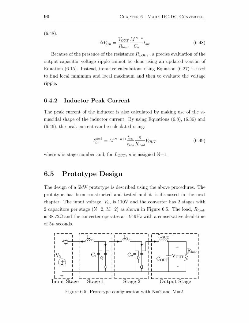
90 Chapter 6 | Marx DC-DC Converter
(6.48).
∆VCn =VOUTRload
MN−n
Cntsw (6.48)
Because of the presence of the resistance RLOUT , a precise evaluation of the
output capacitor voltage ripple cannot be done using an updated version of
Equation (6.15). Instead, iterative calculations using Equation (6.27) is used
to find local minimum and local maximum and then to evaluate the voltage
ripple.
6.4.2 Inductor Peak Current
The peak current of the inductor is also calculated by making use of the si-
nusoidal shape of the inductor current. By using Equations (6.8), (6.36) and
(6.46), the peak current can be calculated using:
IpeakLn = MN−n+1 tswtres
π
Rload
VOUT (6.49)
where n is stage number and, for LOUT , n is assigned N+1.
6.5 Prototype Design
The design of a 5kW prototype is described using the above procedures. The
prototype has been constructed and tested and it is discussed in the next
chapter. The input voltage, VS, is 110V and the converter has 2 stages with
2 capacitors per stage (N=2, M=2) as shown in Figure 6.5. The load, Rload,
is 38.72Ω and the converter operates at 1949Hz with a conservative dead-time
of 5µ seconds.
+
L1
COUT
Rload+
VS VOUTC1
LOUT
Stage 1 Output StageInput Stage
L2
C2
Stage 2
Figure 6.5: Prototype configuration with N=2 and M=2.

Converter Design Guidelines | 91
Table 6.1: Design parameters.Capacitor
Design Selectionvoltage capacitor capacitor voltage
ripple [V] value [uF] value [uF] ripple [V]C1 33 353 360 32.4C2 33 176 160 36.4COUT 15 214 230 14.0
InductorDesign and selection
inductor value [uH] resistance [Ω]L1 8.8 0.01L2 55.6 0.01LOUT 97.0 0.01
The capacitors are selected based on the initial desired voltage ripple shown
under “design” in Table 6.1. However, only a discrete range of capacitor values
are commercially available which forces designers to have certain margin in the
selection process. A higher capacitor value will reduce the voltage ripple but it
will affect the inductor design by increasing its required value. Using Equations
(6.9) and (6.15), the computed capacitor design values are listed in Table 6.1.
The closest commercially available capacitors are listed beside it. The voltage
ripple is then calculated back based on the selected commercially available
capacitor value.
By using Equation (6.19) with Equations (6.20) and (6.21), the inductor
value for L1 and L2 are calculated and they are listed under “design” in Table
6.1. The output inductor LOUT is calculated using the iterative procedure
described earlier.
Table 6.2 lists capacitor voltages and inductor currents calculated using
equations from Section 6.4. The average capacitor voltages are calculated
using Equations (6.45) and (6.47). The capacitor voltage ripple is calculated
using Equation (6.48) and the iterative approach discussed for ∆VCOUT . The
peak currents are also calculated for all the inductor using Equation (6.49).
6.5.1 Simulation Results
The converter has been simulated in PSCAD-EMTDC software package, an
industry-grade software for high voltage power electronic research, using the
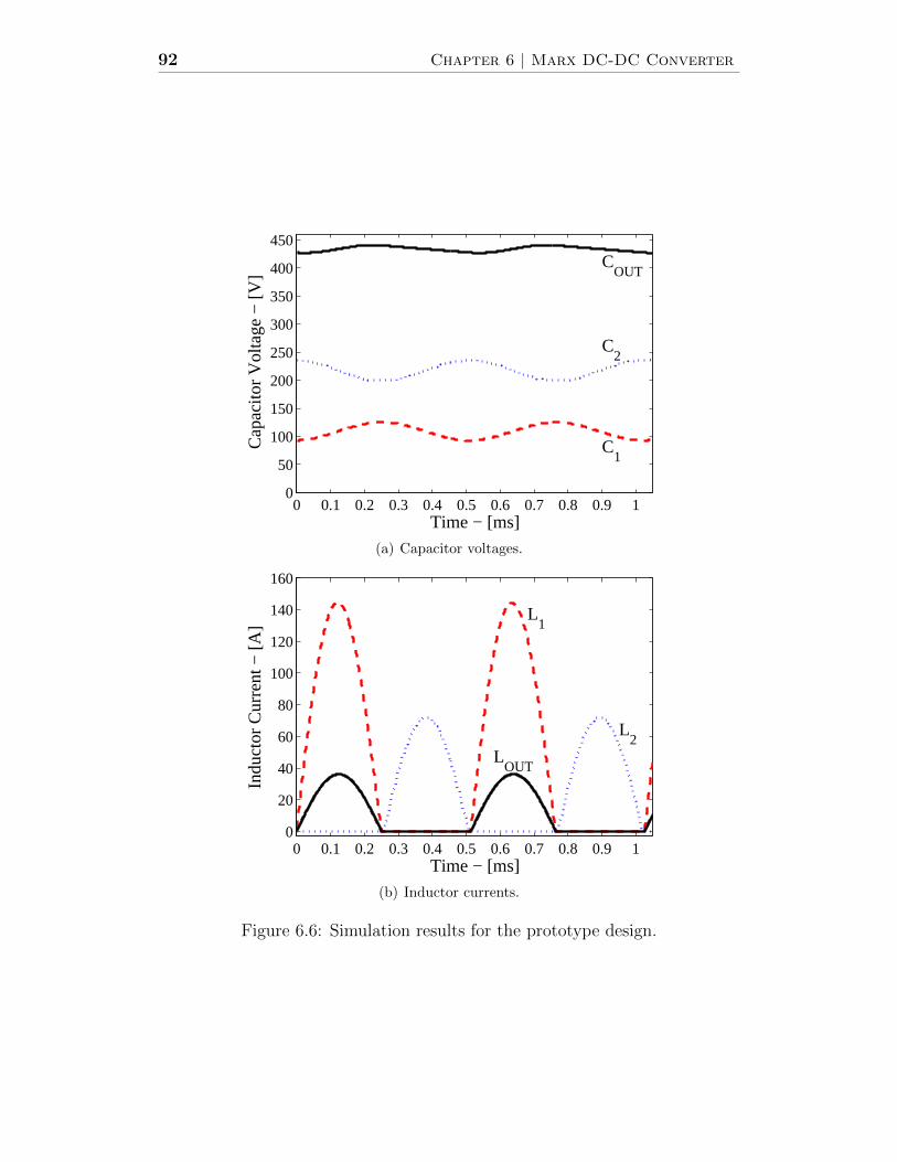
92 Chapter 6 | Marx DC-DC Converter
0 0.1 0.2 0.3 0.4 0.5 0.6 0.7 0.8 0.9 10
50
100
150
200
250
300
350
400
450
Time − [ms]
Cap
acito
r V
olta
ge −
[V] C
OUT
C2
C1
(a) Capacitor voltages.
0 0.1 0.2 0.3 0.4 0.5 0.6 0.7 0.8 0.9 10
20
40
60
80
100
120
140
160
Time − [ms]
Indu
ctor
Cur
rent
− [A
] L1
L2
LOUT
(b) Inductor currents.
Figure 6.6: Simulation results for the prototype design.

Converter Design Guidelines | 93
parameters obtained from the prototype design. The capacitor voltages and
the inductor currents are shown in Figure 6.6. The inductor currents, shown
in Figure 6.6(b), show adequate resonance and the current reaches zero before
the end of each the switching period. The dead-time requirement is respected
with dead-time of 6µs for IL1 and 5µs for IL2 and ILOUT .
In Tables 6.2, the capacitor voltages and the peak currents are noted under
the “simulation results” column and the difference with the design value is
shown. The average capacitor voltages are within 0.5% of the expected value
from the design. By including the losses and the dead-time, the dc voltage
obtained from the simulation is 3.97 as opposed to the theoretical 4. The
capacitor voltage ripple is very accurate for the all stages with results within
0.1V. Regarding the inductor peak current, it is also close to the design value
with difference within 1%. A peak current of 145A is expected for the input
stage in the prototype construction. The peak current decreases by a factor of
2 for each following stages.
Table 6.2: Capacitor voltages and inductor currents.Average Capacitor Voltage
Expected from Simulationdesign results difference
VC1 [V] 109.0 109.2 0.2%VC2 [V] 217.5 216.9 0.3%VCOUT [V] 434.4 434.0 0.1%
Ripple Capacitor VoltageExpected from Simulation
design results difference
∆VC1 [V] 32.0 32.0 0.0%∆VC2 [V] 36.0 36.0 0.0%∆VCOUT [V] 14.0 14.1 0.7%
Inductor Peak CurrentExpected from Simulation
design results difference
IpeakL1 [A] 143.8 144.6 0.6%
IpeakL2 [A] 71.9 71.9 0.0%
IpeakLOUT [A] 35.9 36.2 0.8%

94 Chapter 6 | Marx DC-DC Converter
6.6 Chapter Summary
This chapter has presented a design approach for the Marx converter topology.
The design considers the resistances of the components by modeling them as
an added resistance which affects the resonance. It also introduces a dead-time
requirement in the operation of the converter. The design of the prototype is
used to validate the design guidelines. The prototype is rated for 5kW with 2
stages and 2 capacitors per stage. A good agreement is observed between the
design and the results obtained from the simulation.

Chapter 7
Marx DC-DC Converter:
Experimental Results
(a) Front side of converter. (b) Back side of converter.
Figure 7.1: Prototype converter.
A 5kW prototype converter, shown in Figure 7.1, has been constructed to
acquire experimental results. The experiment has been carried in the power
laboratory at University of Toronto under the supervision of Professor Lehn.
The prototype has been constructed based on the design previously obtained in
Section 6.5 of Chapter 6. However, the inductor has been manually wounded
to respect the resonance period on the setup itself. The discrepancy in the
inductor values between the design and the experiment comes from the imper-
fection of the components which influences the operation of the converter. For
example, the capacitors have a manufacture tolerance from its rated capaci-
tance value and the switches have forward voltage drops as well as additional
95
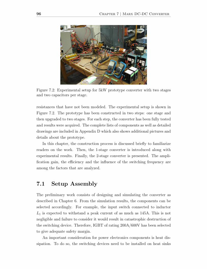
96 Chapter 7 | Marx DC-DC Converter
Figure 7.2: Experimental setup for 5kW prototype converter with two stagesand two capacitors per stage.
resistances that have not been modeled. The experimental setup is shown in
Figure 7.2. The prototype has been constructed in two steps: one stage and
then upgraded to two stages. For each step, the converter has been fully tested
and results were acquired. The complete lists of components as well as detailed
drawings are included in Appendix D which also shows additional pictures and
details about the prototype.
In this chapter, the construction process is discussed briefly to familiarize
readers on the work. Then, the 1-stage converter is introduced along with
experimental results. Finally, the 2-stage converter is presented. The ampli-
fication gain, the efficiency and the influence of the switching frequency are
among the factors that are analyzed.
7.1 Setup Assembly
The preliminary work consists of designing and simulating the converter as
described in Chapter 6. From the simulation results, the components can be
selected accordingly. For example, the input switch connected to inductor
L1 is expected to withstand a peak current of as much as 145A. This is not
negligible and failure to consider it would result in catastrophic destruction of
the switching device. Therefore, IGBT of rating 200A/600V has been selected
to give adequate safety margin.
An important consideration for power electronics components is heat dis-
sipation. To do so, the switching devices need to be installed on heat sinks

Experimental Results | 97
input capacitorsand breakers
LOUTcapacitors
L1 L2
current/voltagesensors
powerelectronics
(a) Prototype converter with inductor andmeasurement devices.
IGBTs
COUT
diodes
C1
C2
gate driverinterface board
heat sinks
(b) Top view of prototype converter withcapacitors and power electronics.
Figure 7.3: Details on experimental setup.
to avoid over-heating. Different models are offered depending on the type of
cooling [78]. The most common is air-cooling with natural or forced convec-
tion. In this project, an air-cooled extrusion heat sink with forced convection
is used and it is shown in the picture of Figure 7.3(b).
The triggering of the IGBTs is done through a gate driver interface board.
The gate driver interface board has to receive small gating signals from an
external controller and to send the high current triggering pulses to the IGBTs.
The gate driver interface board is composed of the gate drivers, which amplify
and isolate the gating signal for each IGBT, and the external circuitry to
interface. For this project, a 6-channel gate driver has been purchased which
provides the required isolation and good performance for triggering the IGBTs.
It is still necessary to design and construct the interface board to supply power
and to set threshold values for dead-time and for levels of protection for the
IGBTs.
A custom-made enclosure has been constructed around the platform upon
which the prototype is built so as to provide necessary safety. One of the
objective in the design is to minimize the distance between the power electronic
components and the capacitors. The inductance of long wire with the capacitor
can create resonance which can impact the behaviour of the power electronic
component. The items located inside the enclosure are: gate driver interface
board, power electronic switches installed on heat sinks, capacitors and fuses.
The components connected outside are: inductors, current sensors and load.
Prior to operating the converter, a start-up procedure has been determined
and tested in simulation software. The start-up procedure is intended to pre-
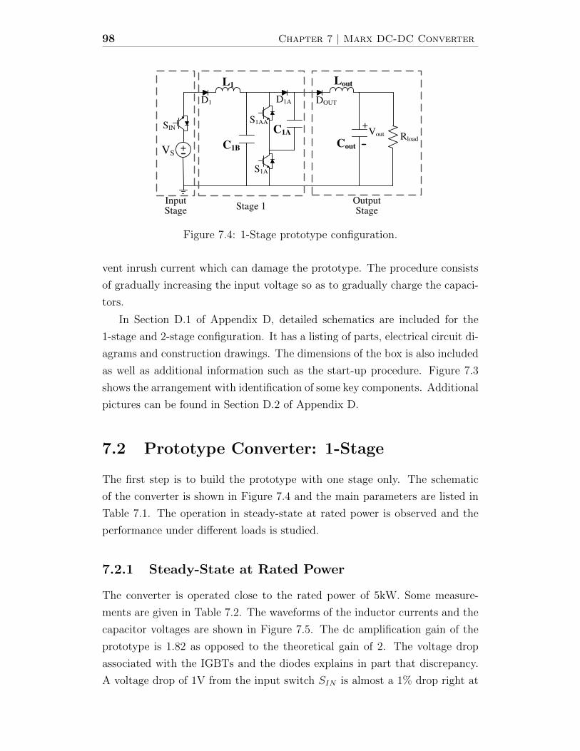
98 Chapter 7 | Marx DC-DC Converter
+
L1Lout
Cout
Rload
+
VS
SIN
D1
S1AA
Vout
C1B
C1A
S1A
DOUTD1A
InputStage Stage 1
OutputStage
Figure 7.4: 1-Stage prototype configuration.
vent inrush current which can damage the prototype. The procedure consists
of gradually increasing the input voltage so as to gradually charge the capaci-
tors.
In Section D.1 of Appendix D, detailed schematics are included for the
1-stage and 2-stage configuration. It has a listing of parts, electrical circuit di-
agrams and construction drawings. The dimensions of the box is also included
as well as additional information such as the start-up procedure. Figure 7.3
shows the arrangement with identification of some key components. Additional
pictures can be found in Section D.2 of Appendix D.
7.2 Prototype Converter: 1-Stage
The first step is to build the prototype with one stage only. The schematic
of the converter is shown in Figure 7.4 and the main parameters are listed in
Table 7.1. The operation in steady-state at rated power is observed and the
performance under different loads is studied.
7.2.1 Steady-State at Rated Power
The converter is operated close to the rated power of 5kW. Some measure-
ments are given in Table 7.2. The waveforms of the inductor currents and the
capacitor voltages are shown in Figure 7.5. The dc amplification gain of the
prototype is 1.82 as opposed to the theoretical gain of 2. The voltage drop
associated with the IGBTs and the diodes explains in part that discrepancy.
A voltage drop of 1V from the input switch SIN is almost a 1% drop right at
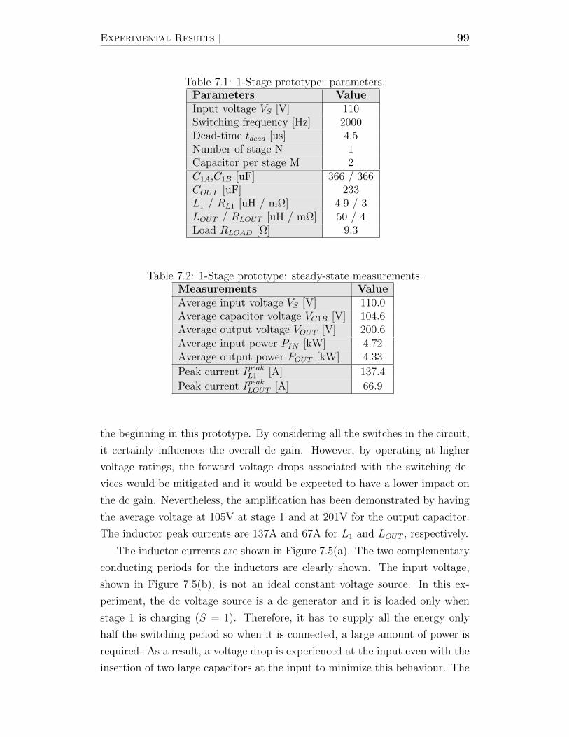
Experimental Results | 99
Table 7.1: 1-Stage prototype: parameters.Parameters ValueInput voltage VS [V] 110Switching frequency [Hz] 2000Dead-time tdead [us] 4.5Number of stage N 1Capacitor per stage M 2C1A,C1B [uF] 366 / 366COUT [uF] 233L1 / RL1 [uH / mΩ] 4.9 / 3LOUT / RLOUT [uH / mΩ] 50 / 4Load RLOAD [Ω] 9.3
Table 7.2: 1-Stage prototype: steady-state measurements.Measurements ValueAverage input voltage VS [V] 110.0Average capacitor voltage VC1B [V] 104.6Average output voltage VOUT [V] 200.6Average input power PIN [kW] 4.72Average output power POUT [kW] 4.33
Peak current IpeakL1 [A] 137.4
Peak current IpeakLOUT [A] 66.9
the beginning in this prototype. By considering all the switches in the circuit,
it certainly influences the overall dc gain. However, by operating at higher
voltage ratings, the forward voltage drops associated with the switching de-
vices would be mitigated and it would be expected to have a lower impact on
the dc gain. Nevertheless, the amplification has been demonstrated by having
the average voltage at 105V at stage 1 and at 201V for the output capacitor.
The inductor peak currents are 137A and 67A for L1 and LOUT , respectively.
The inductor currents are shown in Figure 7.5(a). The two complementary
conducting periods for the inductors are clearly shown. The input voltage,
shown in Figure 7.5(b), is not an ideal constant voltage source. In this ex-
periment, the dc voltage source is a dc generator and it is loaded only when
stage 1 is charging (S = 1). Therefore, it has to supply all the energy only
half the switching period so when it is connected, a large amount of power is
required. As a result, a voltage drop is experienced at the input even with the
insertion of two large capacitors at the input to minimize this behaviour. The

100 Chapter 7 | Marx DC-DC Converter
IL1
ILOUT
(a) Inductor current waveforms.
VS
(b) Input voltage waveform.
VC1B
VC1A
(c) Capacitor voltage waveforms.
VOUT
(d) Output voltage waveform.
Figure 7.5: Experimental results for 1-stage prototype at 5kW.
charging/discharging of the two converter capacitors, C1A and C1B, is shown
in Figure 7.5(c). It is important to note that only the voltage ripples of each
capacitor are shown. The offset between the two waveforms have been manu-
ally adjusted to display both distinctly. Similarly, the output voltage, shown
in Figure 7.5(d), depicts the predicted waveform of the charging phase and
the almost linear discharge. The results obtained from the 1-stage converter
experiment confirms the behaviour of the converter. The waveforms are as
expected and the designed voltage amplification is obtained.
7.2.2 Gain and Efficiency
The converter performance under different load has been tested. The converter
gain and efficiency are shown in Figures 7.6(a) and 7.6(b), respectively. At low
power, the gain is around 1.91 and it decreases to 1.82 at rated power. The
reduction is in the order of 5%. Similarly, the efficiency gradually decreases
from 96.5% to 92.3%. As the power increases, the current is higher which
creates larger voltage drops and higher losses which explains the decrease of
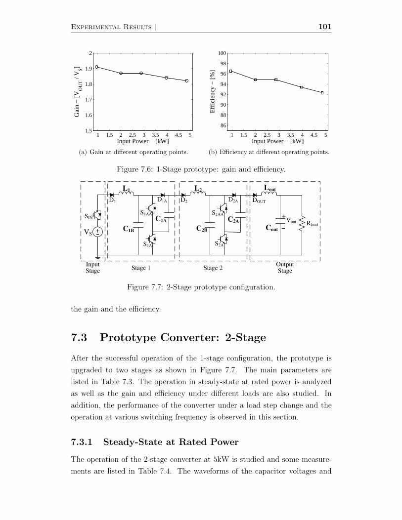
Experimental Results | 101
1 1.5 2 2.5 3 3.5 4 4.5 51.5
1.6
1.7
1.8
1.9
2
Gai
n −
[VO
UT /
VS]
Input Power − [kW]
(a) Gain at different operating points.
1 1.5 2 2.5 3 3.5 4 4.5 5
86
88
90
92
94
96
98
100
Effi
cien
cy −
[%]
Input Power − [kW]
(b) Efficiency at different operating points.
Figure 7.6: 1-Stage prototype: gain and efficiency.
+
L1Lout
Cout
Rload
+
VS
SIN
D1
S1AA
Vout
C1B
C1A
D2
C2B
C2A
S1A S2A
S2AA
DOUTD1A D2A
L2
InputStage Stage 1 Stage 2
OutputStage
Figure 7.7: 2-Stage prototype configuration.
the gain and the efficiency.
7.3 Prototype Converter: 2-Stage
After the successful operation of the 1-stage configuration, the prototype is
upgraded to two stages as shown in Figure 7.7. The main parameters are
listed in Table 7.3. The operation in steady-state at rated power is analyzed
as well as the gain and efficiency under different loads are also studied. In
addition, the performance of the converter under a load step change and the
operation at various switching frequency is observed in this section.
7.3.1 Steady-State at Rated Power
The operation of the 2-stage converter at 5kW is studied and some measure-
ments are listed in Table 7.4. The waveforms of the capacitor voltages and

102 Chapter 7 | Marx DC-DC Converter
VSVC1B
VC2B
VOUT
= 110.6V
Sensor 30:1
= 203.0V
Sensor 30:1
= 397.3 V
Sensor 70:1VC1B VC2B VOUT
(a) Voltage waveforms (manual adjustment of the y-axis scale andoffset for each signal).
IL2
IL1
ILOUT
ILOAD
(b) Inductor current waveforms.
Figure 7.8: Experimental results for 2-stage 5kW prototype.

Experimental Results | 103
Table 7.3: 2-Stage prototype: parameters.Parameters ValueInput voltage VS [V] 110Switching frequency [Hz] 1949Dead-time tdead [us] 4.5Number of stage N 2Capacitor per stage M 2C1A,C1B [uF] 366 / 366C2A,C2B [uF] 151 / 152COUT [uF] 233L1 / RL1 [uH / mΩ] 4.9 / 3L2 / RL2 [uH / mΩ] 50 / 4LOUT / RLOUT [uH / mΩ] 95.3 / 4Load RLOAD [Ω] 34.7
Table 7.4: 2-Stage prototype: steady-state measurements.Measurements ValueAverage input voltage VS [V] 108.8Average capacitor voltage VC1B [V] 101.5Average capacitor voltage VC2B [V] 197.4Average output voltage VOUT [V] 389.9Average input power PIN [kW] 4.63Average output power POUT [kW] 4.38
Peak current IpeakL1 [A] 146.8
Peak current IpeakL2 [A] 74.4
Peak current IpeakLOUT [A] 36.1
inductor currents are shown in Figure 7.8. The dc amplification gain of the
prototype is 3.58 as opposed to the theoretical gain of 4. The amplification has
been demonstrated by having the average voltage at 102V at stage 1, 197V
at stage 2 and at 390V for the output capacitor. Figure 7.8(a) shows that
when C2B is charging, C1B is discharging and vice-versa. The input voltage
VS and the output voltage VOUT have the waveforms similar to Figures 7.5(b)
and 7.5(d) respectively.
Figure 7.8(b) shows the current waveforms. The inductor currents of the
odd-numbered stages (IL1 and ILOUT ) are shown to occur at the same instant.
The even-numbered stage current (IL2) flows in the complementary period.
The inductor currents reach zero before the end of the next switching event in

104 Chapter 7 | Marx DC-DC Converter
1 1.5 2 2.5 3 3.5 4 4.5 53.4
3.5
3.6
3.7
3.8
3.9
4
Gai
n −
[VO
UT /
VS]
Input Power − [kW]
(a) Gain versus power operating point.
1 1.5 2 2.5 3 3.5 4 4.5 5
86
88
90
92
94
96
98
100
Effi
cien
cy −
[%]
Input Power − [kW]
(b) Efficiency versus power operatingpoint.
Figure 7.9: 2-Stage prototype: gain and efficiency.
all three cases. The peak currents are 147A, 74A and 36A for L1, L2 and LOUT ,
respectively. Their values are close to the expected values obtained from the
design done in Section 6.5 of Chapter 6.
7.3.2 Gain and Efficiency
The converter gain and efficiency for different load have been tested and the
results are shown in Figure 7.9. The converter gain decreases more linearly
than for the 1-stage observation. The converter gain decrease by 5% when
comparing the gain under low and rated load condition. The efficiency is at
95% at low load and it reaches 91% at full load. Nevertheless, the efficiency
is above 90% which is good according that the converter is a prototype and it
has not been optimized to minimize losses.
7.3.3 Load Step Change
A disturbance has been applied to the system to evaluate its stability. A step
change has been performed at the output load and the response is shown in
Figure 7.10. The load has been decreased from 66Ω to 36Ω which represents an
increase in power from 2.8kW to 4.9kW. From Figure 7.10, the output current
ILOAD has a step increase corresponding to the step increase in the load. The
large drain in current from the output capacitor decreases the output voltage
VOUT . It takes two cycles for the change to appear at the input current, IL1.
The delay corresponds to the number of stages in the system.
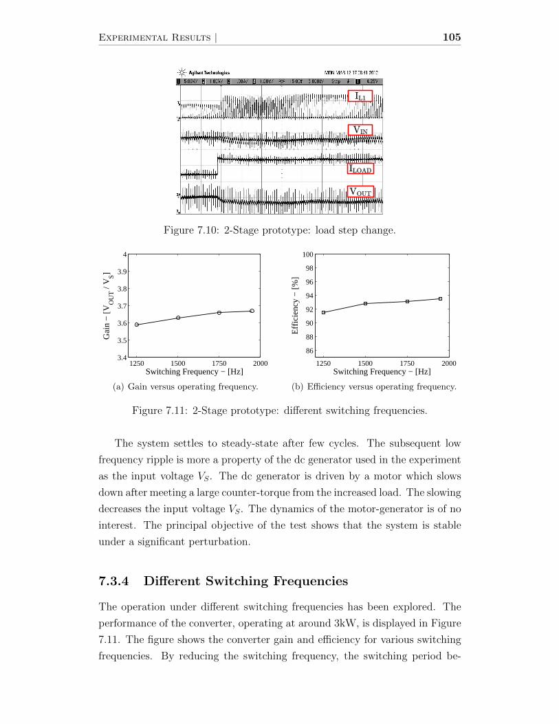
Experimental Results | 105
IL1
VIN
ILOAD
VOUT
Figure 7.10: 2-Stage prototype: load step change.
1250 1500 1750 20003.4
3.5
3.6
3.7
3.8
3.9
4
Gai
n −
[VO
UT /
VS]
Switching Frequency − [Hz]
(a) Gain versus operating frequency.
1250 1500 1750 2000
86
88
90
92
94
96
98
100
Effi
cien
cy −
[%]
Switching Frequency − [Hz]
(b) Efficiency versus operating frequency.
Figure 7.11: 2-Stage prototype: different switching frequencies.
The system settles to steady-state after few cycles. The subsequent low
frequency ripple is more a property of the dc generator used in the experiment
as the input voltage VS. The dc generator is driven by a motor which slows
down after meeting a large counter-torque from the increased load. The slowing
decreases the input voltage VS. The dynamics of the motor-generator is of no
interest. The principal objective of the test shows that the system is stable
under a significant perturbation.
7.3.4 Different Switching Frequencies
The operation under different switching frequencies has been explored. The
performance of the converter, operating at around 3kW, is displayed in Figure
7.11. The figure shows the converter gain and efficiency for various switching
frequencies. By reducing the switching frequency, the switching period be-
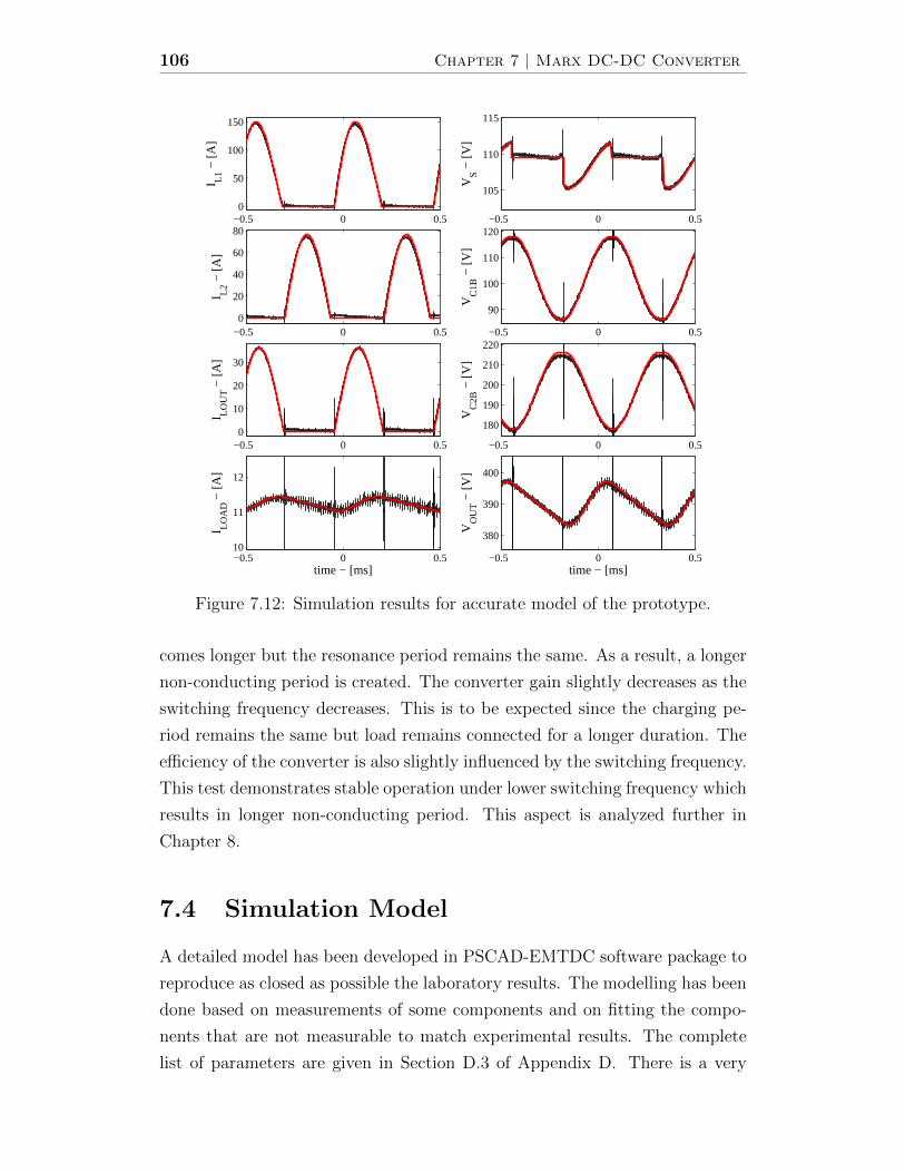
106 Chapter 7 | Marx DC-DC Converter
−0.5 0 0.50
50
100
150
I L1 −
[A]
−0.5 0 0.50
20
40
60
80I L2
− [A
]
−0.5 0 0.50
10
20
30
I LOU
T −
[A]
−0.5 0 0.510
11
12
I LOA
D −
[A]
time − [ms]
−0.5 0 0.5
105
110
115
VS −
[V]
−0.5 0 0.5
90
100
110
120
VC
1B −
[V]
−0.5 0 0.5
180
190
200
210
220
VC
2B −
[V]
−0.5 0 0.5
380
390
400V
OU
T − [V
]
time − [ms]
Figure 7.12: Simulation results for accurate model of the prototype.
comes longer but the resonance period remains the same. As a result, a longer
non-conducting period is created. The converter gain slightly decreases as the
switching frequency decreases. This is to be expected since the charging pe-
riod remains the same but load remains connected for a longer duration. The
efficiency of the converter is also slightly influenced by the switching frequency.
This test demonstrates stable operation under lower switching frequency which
results in longer non-conducting period. This aspect is analyzed further in
Chapter 8.
7.4 Simulation Model
A detailed model has been developed in PSCAD-EMTDC software package to
reproduce as closed as possible the laboratory results. The modelling has been
done based on measurements of some components and on fitting the compo-
nents that are not measurable to match experimental results. The complete
list of parameters are given in Section D.3 of Appendix D. There is a very

Experimental Results | 107
good agreement between the simulation model and the recorded data. The
validity of the model has been compared with the steady-state operation as
shown in Figure 7.12. The errors are within 1% for most signals and the main
discrepancy is located in the peak inductor current. Some of the discrepancies
can be explained by the non-linear behaviour of the components with respect
to thermal impact. Nevertheless, the accurate model could be used for future
study of the prototype.
7.5 Chapter Summary
In this chapter, a 5kW prototype converter has been presented. Initially,
the converter has been tested for one stage before upgrading to the 2-stage
configuration. The 2-stage configuration has two capacitors per stage for a
theoretical dc voltage gain of four. Operation under different loads, different
switching frequency and load step change are among the tests performed on the
prototype. The prototype is stable and it amplifies the dc voltage as expected.
The laboratory experiment is very successful with respect to the concept and
design of the converter.

108 Chapter 7 | Marx DC-DC Converter

Chapter 8
Marx DC-DC Converter:
Stability Analysis and
Parameter Ratings
This chapter presents the stability analysis of the Marx converter. Simula-
tion and experimental results have shown the converter to be stable but it has
been observed only for a short period of time. The stability analysis tests the
system for t →∞ with the objective to determine if the system is asymptot-
ically stable [76]. Firstly, the operation under continuous conduction mode is
explored and followed by the discontinuous conduction mode. In both modes,
it is shown that the converter is stable.
The second part of the chapter presents a guide to the evaluation of the
parameter ratings. Equations are derived which give good estimations of the
component ratings for a Marx converter of N stages with M capacitors per
stage. The components evaluated are: IGBTs, diodes, inductors and capaci-
tors.
8.1 Stability Analysis
A stability analysis is performed to evaluate the dynamic behaviour of the sys-
tem. The analysis is similar to sampled-data approach used in control theory
since the converter operates in repetitive sequence of states of equal dura-
tion [76]. In each state configuration, or sub-period, the system is composed
of a set of linear equations.
109
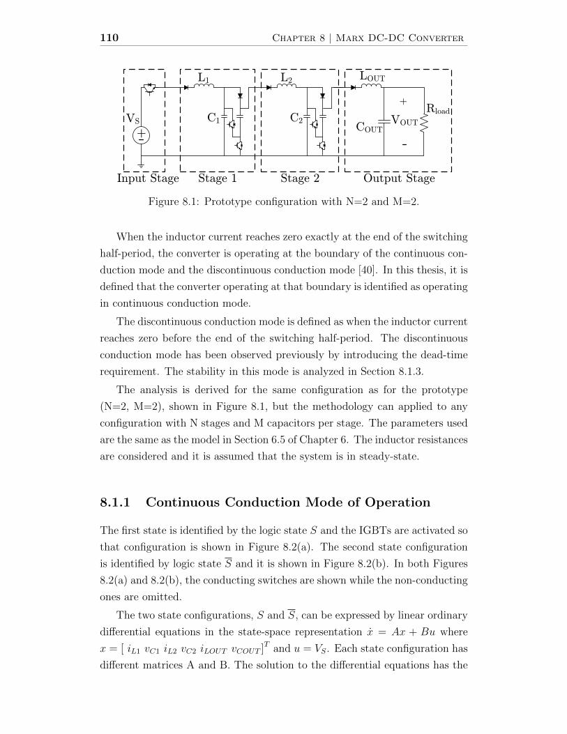
110 Chapter 8 | Marx DC-DC Converter
+
L1
COUT
Rload+
VS VOUTC1
LOUT
Stage 1 Output StageInput Stage
L2
C2
Stage 2
Figure 8.1: Prototype configuration with N=2 and M=2.
When the inductor current reaches zero exactly at the end of the switching
half-period, the converter is operating at the boundary of the continuous con-
duction mode and the discontinuous conduction mode [40]. In this thesis, it is
defined that the converter operating at that boundary is identified as operating
in continuous conduction mode.
The discontinuous conduction mode is defined as when the inductor current
reaches zero before the end of the switching half-period. The discontinuous
conduction mode has been observed previously by introducing the dead-time
requirement. The stability in this mode is analyzed in Section 8.1.3.
The analysis is derived for the same configuration as for the prototype
(N=2, M=2), shown in Figure 8.1, but the methodology can applied to any
configuration with N stages and M capacitors per stage. The parameters used
are the same as the model in Section 6.5 of Chapter 6. The inductor resistances
are considered and it is assumed that the system is in steady-state.
8.1.1 Continuous Conduction Mode of Operation
The first state is identified by the logic state S and the IGBTs are activated so
that configuration is shown in Figure 8.2(a). The second state configuration
is identified by logic state S and it is shown in Figure 8.2(b). In both Figures
8.2(a) and 8.2(b), the conducting switches are shown while the non-conducting
ones are omitted.
The two state configurations, S and S, can be expressed by linear ordinary
differential equations in the state-space representation x = Ax + Bu where
x = [ iL1 vC1 iL2 vC2 iLOUT vCOUT ]T and u = VS. Each state configuration has
different matrices A and B. The solution to the differential equations has the

Stability Analysis and Parameter Ratings | 111
+
L1
COUT
RloadVS C1
LOUT
Stage 1 Output StageInput Stage
L2
C2
Stage 2
(a) Configuration with logic state S.
+
L1
COUT
RloadVS C1
LOUT
Stage 1 Output StageInput Stage
L2
C2
Stage 2
(b) Configuration with logic state S.
Figure 8.2: Converter state configurations with conducting switches displayed.
form:
x(t) = Ux(t0) + V u(t0) (8.1)
where,
U = eA(t−t0) (8.2)
and
V = A−1(eA(t−t0) − I
)B (8.3)
The matrix A needs to be non-singular to compute its inverse in Equa-
tion (8.3). However, the inductors are used only during one of the two state
configurations of the converter operation. As a result, the matrix A becomes
singular because of zero rows/columns associated with the current iL of the dis-
connected inductor. To encounter this computation issue, the inverse is done
by using the Moore-Penrose generalized inverse, also known as pseudoinverse,
which makes use of the least squares solution of the set of equations [79]. In
this situation, the solution is equivalent to matrix manipulations of eliminat-
ing zero vectors prior to invert, followed by reconstructing from the inverted
matrix to match initial matrix size.
The matrix notation for the system in state configuration S is A1, B1, U1

112 Chapter 8 | Marx DC-DC Converter
and V1. Similarly for state configuration S, matrices have notation A2, B2,
U2 and V2. The operation of the converter is divided into two states of equal
duration tsw/2. Starting in state configuration S at t=0, the solution is:
x
(tsw2
)= U1x(0) + V1u(0) (8.4)
where U1 = eA1tsw2 and V1 = A−1
1
(eA1
tsw2 − I
)B1. Then, from t = tsw/2 to
t = tsw, the converter is in state configuration S. It gives:
x (tsw) = U2x
(tsw2
)+ V2u
(tsw2
)(8.5)
where U2 = eA2tsw2 and V2 = A−1
2
(eA2
tsw2 − I
)B2. From Figure 8.2(b), it is
clear that the input voltage source VS is disconnected during S. Therefore,
the matrix V2 is zero because B2 is a zero vector. Therefore, Equation (8.5) is
simplified and by combining with Equation (8.4), it gives:
x (tsw) = U2U1x(0) + U2V1u(0) (8.6)
By defining ψ = U2U1 and Φ = U2V1, Equation (8.6) is rewritten as:
x (tsw) = ψx(0) + Φu(0) (8.7)
A general solution is obtained with q = ntsw, n being an integer number:
x(q + 1) = ψq+1x(0) + ψqΦu(0) + ψq−1Φu(1) + · · ·+ Φu(q) (8.8)
For the case under study, the input u is the constant voltage source VS, so
Equation (8.8) is rearranged to:
x(q + 1) = ψq+1x(0) +I + ψ1 + · · ·+ ψq−1 + ψq
ΦVS (8.9)
The finite geometric series I + ψ1 + · · ·+ ψq−1 + ψq equals to [80]:
q∑n=0
ψn = (I − ψ)−1 [I − ψq+1]
(8.10)
If q →∞ , the series converges if and only if |ψ| ≤ 1. Using Equation (8.10),

Stability Analysis and Parameter Ratings | 113
Equation (8.9) becomes:
x(q + 1) = ψq+1x(0) + (I − ψ)−1 [I − ψq+1]
ΦVS (8.11)
Stability is determined by the eigenvalues of ψ. By having the eigenvalues of
ψ within the complex unit circle, the converter is stable. Even if the system is
continuous within each state configuration, the analysis is referring to discrete
instant or more precisely every switching period as stated for Equation (8.11).
Therefore, the unit circle in the complex plane is used for stability instead of
the jω-axis.
8.1.2 Example
The stability analysis is applied to the prototype model. Because this analysis
considers continuous conduction mode, the duration tres will be considered
instead of tsw because the selected tsw included a dead-time segment. By
doing so, the switching frequency used is 1988Hz instead of 1949Hz.
For the system in state configuration S, referring to Figure 8.2(a), the
matrices A1 and B1 are:
A1 =
−RL1
L1
−1L1
0 0 0 01
MC10 0 0 0 0
0 0 0 0 0 0
0 0 0 0 −1C2
0
0 0 0 MLOUT
−RLOUT
LOUT
−1LOUT
0 0 0 0 1COUT
−1COUTRload
(8.12)
B1 =[
1L1
0 0 0 0 0]T
(8.13)
For state configuration S, referring to Figure 8.2(b), the matrices A2 and B2
are:
A2 =
0 0 0 0 0 0
0 0 −1C1
0 0 0
0 ML2
−RL2
L2
−1L2
0 0
0 0 1MC2
0 0 0
0 0 0 0 0 −1COUTRload
(8.14)
B2 =[
0 0 0 0 0 0]T
(8.15)

114 Chapter 8 | Marx DC-DC Converter
−1 −0.5 0 0.5 1
−1
−0.5
0
0.5
1
Real Axis
Imag
inar
y A
xis
Eigenvalues of ψ
Figure 8.3: Eigenvalues of ψ for operation in continuous conduction mode.
Table 8.1: Eigenvalues of ψ and ψ.Continuous Discontinuous
conduction mode conduction mode(fsw = 1988Hz) (fsw = 1789Hz)
λ1,2 ( |λ1,2| ) 0.748 ± i0.531 (0.918) 0.746 ± i0.530 (0.916)λ3,4 ( |λ3,4| ) -0.953 ± i0.138 (0.963) -0.952 ± i0.138 (0.962)λ5 ( |λ5| ) -0.867 (0.867) -0.867 (0.867)λ6 ( |λ6| ) -0.978 (0.978) -0.978 (0.978)
Based on Equation (8.11), the eigenvalues of ψ is calculated and it is given
in Table 8.1 under the column continuous conduction mode. It can be seen
that all eigenvalues are within the complex unit circle, as shown in Figure 8.3,
which confirms stability of the converter. The eigenvalues are very close to the
unit circle and it is due to the small resistance in the system. By increasing
RL, the eigenvalues have been observed to move toward the center.
8.1.3 Discontinuous Conduction Mode of Operation
The converter enters in discontinuous conduction mode of operation when the
inductor current reaches zero prior the end of the switching instant. The induc-
tor waveforms of the converter in discontinuous conduction mode are shown
in Figure 8.4. Each state configuration of duration tsw/2 is now subdivided
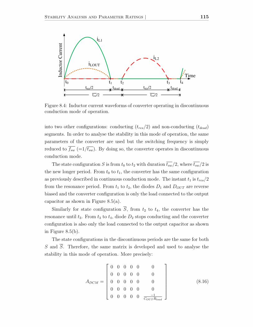
Stability Analysis and Parameter Ratings | 115
iL1
iL2
t0 t2 t4
Ind
ucto
rC
urr
en
t
Time
iLOUT
t1 t3
tsw/2
tres/2 tdead
tsw/2
tres/2 tdead
Figure 8.4: Inductor current waveforms of converter operating in discontinuousconduction mode of operation.
into two other configurations: conducting (tres/2) and non-conducting (tdead)
segments. In order to analyse the stability in this mode of operation, the same
parameters of the converter are used but the switching frequency is simply
reduced to fsw (=1/tsw). By doing so, the converter operates in discontinuous
conduction mode.
The state configuration S is from t0 to t2 with duration tsw/2, where tsw/2 is
the new longer period. From t0 to t1, the converter has the same configuration
as previously described in continuous conduction mode. The instant t1 is tres/2
from the resonance period. From t1 to t2, the diodes D1 and DOUT are reverse
biased and the converter configuration is only the load connected to the output
capacitor as shown in Figure 8.5(a).
Similarly for state configuration S, from t2 to t4, the converter has the
resonance until t3. From t3 to t4, diode D2 stops conducting and the converter
configuration is also only the load connected to the output capacitor as shown
in Figure 8.5(b).
The state configurations in the discontinuous periods are the same for both
S and S. Therefore, the same matrix is developed and used to analyse the
stability in this mode of operation. More precisely:
ADCM =
0 0 0 0 0 0
0 0 0 0 0 0
0 0 0 0 0 0
0 0 0 0 0 0
0 0 0 0 0 −1COUTRload
(8.16)

116 Chapter 8 | Marx DC-DC Converter
+
L1
COUT
RloadVS C1
LOUT
Stage 1 Output StageInput Stage
L2
C2
Stage 2
(a) Discontinuous conduction configuration with logic state S
+
L1
COUT
RloadVS C1
LOUT
Stage 1 Output StageInput Stage
L2
C2
Stage 2
(b) Discontinuous conduction configuration with logic state S.
Figure 8.5: State configurations for discontinuous conduction segment of theconverter in during logic states S and S.
BDCM =[
0 0 0 0 0 0]T
(8.17)
The discontinuous segment is the same in both cases. Therefore, they have
the same UDCM where:
UDCM = eADCM (tdead) (8.18)
The new matrix ψ becomes:
ψ = UDCMU2UDCMU1 (8.19)
where U1 and U2 were defined for the continuous conduction mode.
Using the same model for the continuous conduction mode example, the
switching frequency is decreased to 1789Hz to analyse the stability of the con-
verter operating in discontinuous conduction mode. The relative discontinuous
period for the converter becomes 10%. The new eigenvalues of ψ are listed in
Table 8.1. The magnitudes of λ1,2 and λ3,4 are slightly decreasing and they all
remain inside the unit circle. The eigenvalues λ5 and λ6 are not affected by
the discontinuous mode. This analysis confirms the stability of the system in
both continuous and discontinuous conduction modes.

Stability Analysis and Parameter Ratings | 117
8.2 Parameter Ratings
This section evaluates the power rating of the components in the Marx con-
verter topology. The analysis covers a configuration of N stages with M capac-
itors per stage. The volt-amp rating is evaluated by the peak current flowing
in the component and the maximum withstand voltage across the component.
The general expression is:
VARATING = [Ipeak]× [V max] (8.20)
The voltage withstand considered is the voltage across the device. The voltage
with respect to ground is related to insulation coordination and it is not in the
scope of this thesis. Some assumptions and approximations are made in the
analysis which are:
• Each stage has the same number of capacitor M.
• The converter is assumed to operate in steady-state.
• Inductor losses and dead-time requirements are neglected.
• When two components are connected in series, voltage sharing is not
considered. It is assumed that each component should withstand the
complete voltage.
• The voltage ripple ∆VCn is the peak to peak voltage ripple and the same
relative voltage ripple is assumed. Recalling Equation (5.23), the relation
for the same relative capacitor voltage ripple is:
∆VCn = Mn−1∆VC1 (8.21)
The base current for the peak current evaluation is the peak current of inductor
in stage 1. It is labelled as “IP” in this analysis and it is calculated using
Equation (8.22) derived from Equations (6.3) and (6.49) with the assumptions
given preivously.
IP = M2NπVSRload
(8.22)
The power electronic components evaluated are IGBTs and diodes. For the
passive components, capacitors and inductors are considered. Figure 8.6 shows
a detailed model of stage n with M capacitors. Each capacitor is located on
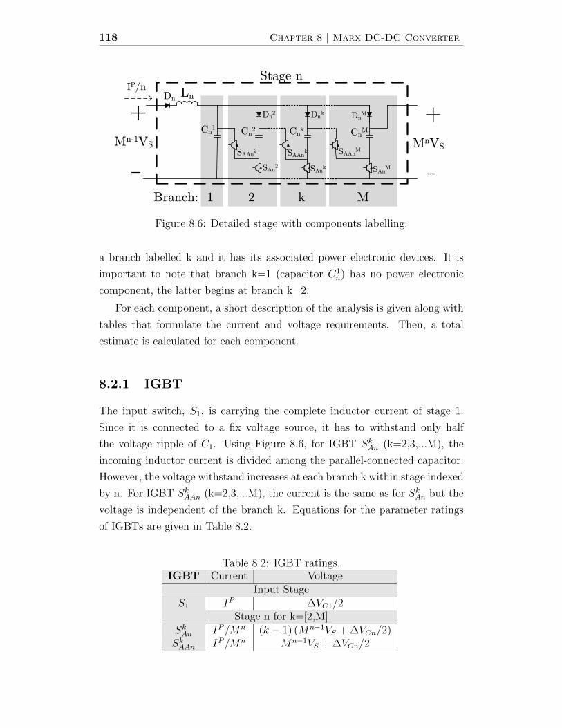
118 Chapter 8 | Marx DC-DC Converter
Ln
Stage n
Cn1 Cn2 CnM
Dn
SAAn2 SAAnM
SAn2 SAnM
Dn2 DnM
Cnk
SAAnk
SAnk
Dnk
Branch: 1 2 k M
+Mn-1VS
+MnVS
IP/n
Figure 8.6: Detailed stage with components labelling.
a branch labelled k and it has its associated power electronic devices. It is
important to note that branch k=1 (capacitor C1n) has no power electronic
component, the latter begins at branch k=2.
For each component, a short description of the analysis is given along with
tables that formulate the current and voltage requirements. Then, a total
estimate is calculated for each component.
8.2.1 IGBT
The input switch, S1, is carrying the complete inductor current of stage 1.
Since it is connected to a fix voltage source, it has to withstand only half
the voltage ripple of C1. Using Figure 8.6, for IGBT SkAn (k=2,3,...M), the
incoming inductor current is divided among the parallel-connected capacitor.
However, the voltage withstand increases at each branch k within stage indexed
by n. For IGBT SkAAn (k=2,3,...M), the current is the same as for SkAn but the
voltage is independent of the branch k. Equations for the parameter ratings
of IGBTs are given in Table 8.2.
Table 8.2: IGBT ratings.IGBT Current Voltage
Input StageS1 IP ∆VC1/2
Stage n for k=[2,M]SkAn IP/Mn (k − 1) (Mn−1VS + ∆VCn/2)SkAAn IP/Mn Mn−1VS + ∆VCn/2
Stability Analysis and Parameter Ratings | 119
The general expressions for volt-amp rating are:
VAS1 =[IP]
[∆VC1/2] (8.23)
VASA(n, k) =
[IP
Mn
] [(k − 1)
(Mn−1VS + ∆VCn/2
)](8.24)
for n = [1 : N ] and k = [2 : M ],
VASAA(n, k) =
[IP
Mn
] [Mn−1VS + ∆VCn/2
](8.25)
for n = [1 : N ] and k = [2 : M ]. The volt-amp rating of IGBT VASA per stage
is:
VASA(n) = ΣMk=2VASA(n, k)
= ΣMk=2(k − 1)
[IP
Mn
] [Mn−1VS + ∆VCn/2
](8.26)
The arithmetic series ΣMk=2(k − 1) can be expressed as [80]:
ΣMk=2(k − 1) =
1
2M(M − 1) (8.27)
which gives:
VASA(n) =1
2M(M − 1)
[IP
Mn
] [Mn−1VS + ∆VCn/2
](8.28)
Similarly, for VASAA(n):
VASAA(n) = ΣMk=2VASAA(n, k)
= (M − 1)
[IP
Mn
] [Mn−1VS + ∆VCn/2
](8.29)
The sum of VASA(n) and VASAA(n) gives an expression of the volt-amp rating
of IGBT at stage n:
VAIGBTRATING(n) = (
1
2M + 1)(M − 1)
[IP
Mn
] [Mn−1VS + ∆VCn/2
](8.30)
for n = [1, N ]. By using the assumption of the same relative capacitor voltage
ripple, Equation (8.21) is substituted in Equation (8.30) to get Equation (8.31)
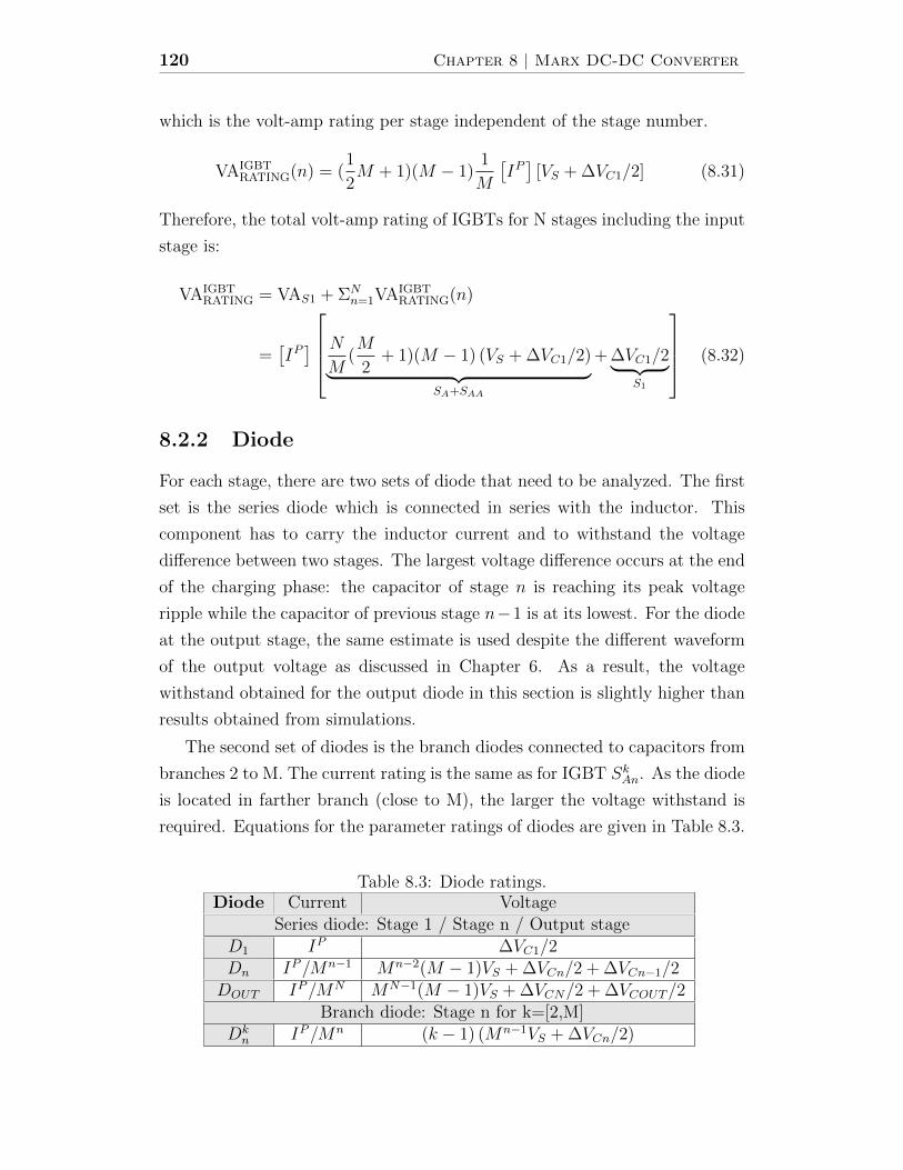
120 Chapter 8 | Marx DC-DC Converter
which is the volt-amp rating per stage independent of the stage number.
VAIGBTRATING(n) = (
1
2M + 1)(M − 1)
1
M
[IP]
[VS + ∆VC1/2] (8.31)
Therefore, the total volt-amp rating of IGBTs for N stages including the input
stage is:
VAIGBTRATING = VAS1 + ΣN
n=1VAIGBTRATING(n)
=[IP] NM (
M
2+ 1)(M − 1) (VS + ∆VC1/2)︸ ︷︷ ︸
SA+SAA
+ ∆VC1/2︸ ︷︷ ︸S1
(8.32)
8.2.2 Diode
For each stage, there are two sets of diode that need to be analyzed. The first
set is the series diode which is connected in series with the inductor. This
component has to carry the inductor current and to withstand the voltage
difference between two stages. The largest voltage difference occurs at the end
of the charging phase: the capacitor of stage n is reaching its peak voltage
ripple while the capacitor of previous stage n−1 is at its lowest. For the diode
at the output stage, the same estimate is used despite the different waveform
of the output voltage as discussed in Chapter 6. As a result, the voltage
withstand obtained for the output diode in this section is slightly higher than
results obtained from simulations.
The second set of diodes is the branch diodes connected to capacitors from
branches 2 to M. The current rating is the same as for IGBT SkAn. As the diode
is located in farther branch (close to M), the larger the voltage withstand is
required. Equations for the parameter ratings of diodes are given in Table 8.3.
Table 8.3: Diode ratings.Diode Current Voltage
Series diode: Stage 1 / Stage n / Output stageD1 IP ∆VC1/2Dn IP/Mn−1 Mn−2(M − 1)VS + ∆VCn/2 + ∆VCn−1/2DOUT IP/MN MN−1(M − 1)VS + ∆VCN/2 + ∆VCOUT/2
Branch diode: Stage n for k=[2,M]Dkn IP/Mn (k − 1) (Mn−1VS + ∆VCn/2)
Stability Analysis and Parameter Ratings | 121
The general expressions for volt-amp rating of series diode are:
VAseriesD1 =
[IP]
[∆VC1/2] (8.33)
VAseriesD (n) =
[IP
Mn−1
] [Mn−2(M − 1)VS + ∆VCn/2 + ∆VCn−1/2
](8.34)
for n = [2 : N ],
VAseriesDOUT =
[IP
MN
] [MN−1(M − 1)VS + ∆VCN/2 + ∆VCOUT/2
](8.35)
By using the assumption of the same relative capacitor voltage ripple, Equation
(8.21) is substituted in Equations (8.34) and (8.35) to derive Equation (8.36),
valid for n = [2 : N ], and Equation (8.37).
VAseriesRATING(n) =
[IP] [(
1− 1
M
)VS +
(1 +
1
M
)∆VC1/2
](8.36)
VAseriesDOUT =
[IP] [(
1− 1
M
)VS +
(1 +
1
M
)∆VC1/2
](8.37)
The volt-amp rating for the branch diode is:
VAbranchD (n, k) =
[IP
Mn
] [(k − 1)
(Mn−1VS + ∆VCn/2
)](8.38)
for n = [1 : N ] and k = [2 : M ]. The volt-amp rating for the branch diode per
stage is:
VAbranchRATING(n) = ΣM
k=2VAbranchD (n, k)
= ΣMk=2(k − 1)
[IP
Mn
] [Mn−1VS + ∆VCn/2
](8.39)
Using Equation (8.27), it gives:
VAbranchRATING(n) =
1
2M(M − 1)
[IP
Mn
] [Mn−1VS + ∆VCn/2
](8.40)
By using the assumption of the same relative capacitor voltage ripple, Equation
(8.21) is substituted and Equation (8.41) is obtained.
VAbranchRATING(n) =
1
2(M − 1)
[IP]
[VS + ∆VC1/2] (8.41)
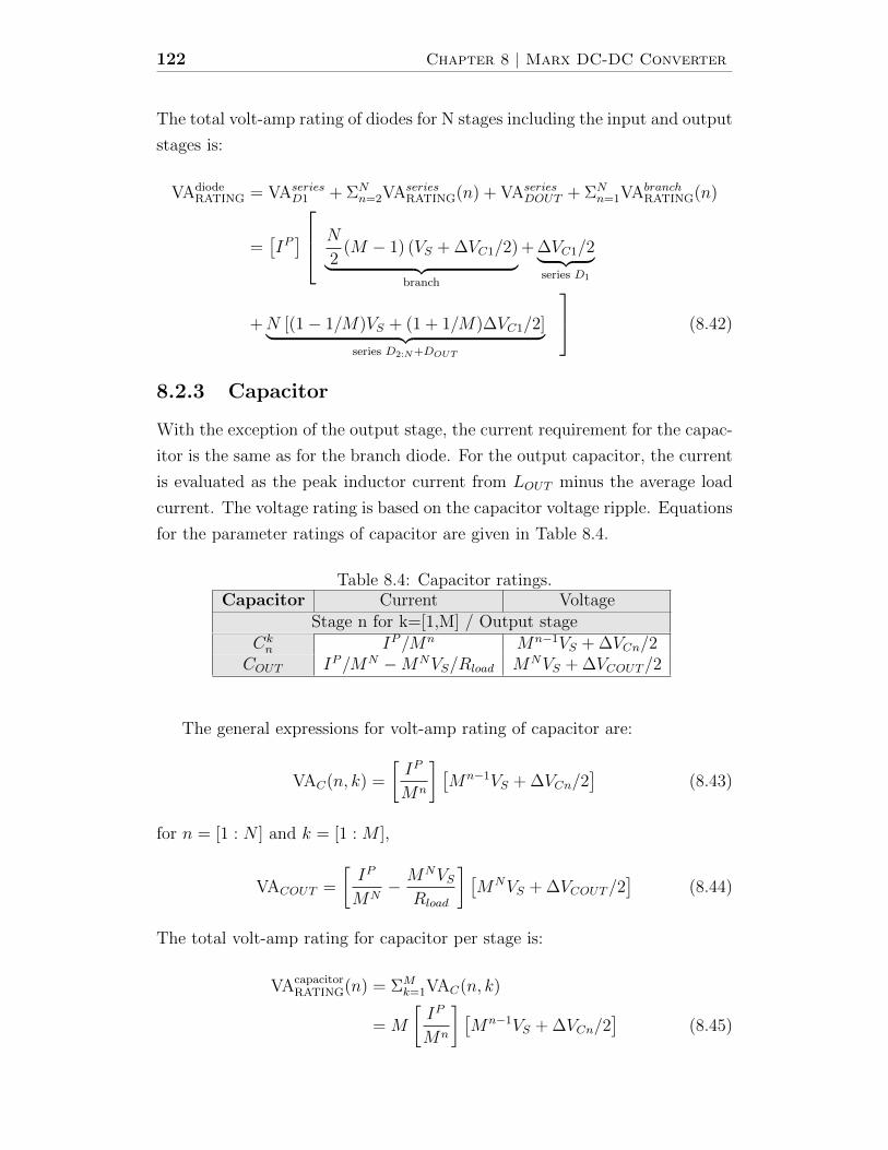
122 Chapter 8 | Marx DC-DC Converter
The total volt-amp rating of diodes for N stages including the input and output
stages is:
VAdiodeRATING = VAseries
D1 + ΣNn=2VAseries
RATING(n) + VAseriesDOUT + ΣN
n=1VAbranchRATING(n)
=[IP] N
2(M − 1) (VS + ∆VC1/2)︸ ︷︷ ︸
branch
+ ∆VC1/2︸ ︷︷ ︸series D1
+N [(1− 1/M)VS + (1 + 1/M)∆VC1/2]︸ ︷︷ ︸series D2:N+DOUT
(8.42)
8.2.3 Capacitor
With the exception of the output stage, the current requirement for the capac-
itor is the same as for the branch diode. For the output capacitor, the current
is evaluated as the peak inductor current from LOUT minus the average load
current. The voltage rating is based on the capacitor voltage ripple. Equations
for the parameter ratings of capacitor are given in Table 8.4.
Table 8.4: Capacitor ratings.Capacitor Current Voltage
Stage n for k=[1,M] / Output stageCkn IP/Mn Mn−1VS + ∆VCn/2
COUT IP/MN −MNVS/Rload MNVS + ∆VCOUT/2
The general expressions for volt-amp rating of capacitor are:
VAC(n, k) =
[IP
Mn
] [Mn−1VS + ∆VCn/2
](8.43)
for n = [1 : N ] and k = [1 : M ],
VACOUT =
[IP
MN− MNVS
Rload
] [MNVS + ∆VCOUT/2
](8.44)
The total volt-amp rating for capacitor per stage is:
VAcapacitorRATING(n) = ΣM
k=1VAC(n, k)
= M
[IP
Mn
] [Mn−1VS + ∆VCn/2
](8.45)
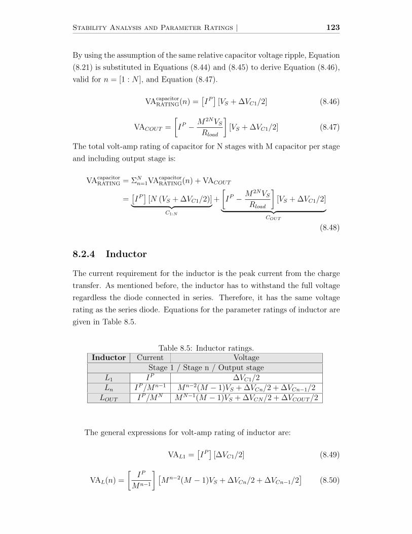
Stability Analysis and Parameter Ratings | 123
By using the assumption of the same relative capacitor voltage ripple, Equation
(8.21) is substituted in Equations (8.44) and (8.45) to derive Equation (8.46),
valid for n = [1 : N ], and Equation (8.47).
VAcapacitorRATING(n) =
[IP]
[VS + ∆VC1/2] (8.46)
VACOUT =
[IP − M2NVS
Rload
][VS + ∆VC1/2] (8.47)
The total volt-amp rating of capacitor for N stages with M capacitor per stage
and including output stage is:
VAcapacitorRATING = ΣN
n=1VAcapacitorRATING(n) + VACOUT
=[IP]
[N (VS + ∆VC1/2)]︸ ︷︷ ︸C1:N
+
[IP − M2NVS
Rload
][VS + ∆VC1/2]︸ ︷︷ ︸
COUT
(8.48)
8.2.4 Inductor
The current requirement for the inductor is the peak current from the charge
transfer. As mentioned before, the inductor has to withstand the full voltage
regardless the diode connected in series. Therefore, it has the same voltage
rating as the series diode. Equations for the parameter ratings of inductor are
given in Table 8.5.
Table 8.5: Inductor ratings.Inductor Current Voltage
Stage 1 / Stage n / Output stageL1 IP ∆VC1/2Ln IP/Mn−1 Mn−2(M − 1)VS + ∆VCn/2 + ∆VCn−1/2LOUT IP/MN MN−1(M − 1)VS + ∆VCN/2 + ∆VCOUT/2
The general expressions for volt-amp rating of inductor are:
VAL1 =[IP]
[∆VC1/2] (8.49)
VAL(n) =
[IP
Mn−1
] [Mn−2(M − 1)VS + ∆VCn/2 + ∆VCn−1/2
](8.50)

124 Chapter 8 | Marx DC-DC Converter
for n = [2 : N ],
VALOUT =
[IP
MN
] [MN−1(M − 1)VS + ∆VCN/2 + ∆VCOUT/2
](8.51)
By using the assumption of the same relative capacitor voltage ripple, Equation
(8.21) is substituted in Equations (8.50) and (8.51) to derive Equation (8.52),
valid for n = [2 : N ], and Equation (8.53).
VAL(n) =[IP] [(
1− 1
M
)VS +
(1 +
1
M
)∆VC1/2
](8.52)
VALOUT =[IP] [(
1− 1
M
)VS +
(1 +
1
M
)∆VC1/2
](8.53)
The total volt-amp rating for the inductor is:
VAinductorRATING = VAL1 + ΣN
n=2VAL(n) + VALOUT
=[IP] ∆VC1/2︸ ︷︷ ︸
L1
+N
[(1− 1
M)VS + (1 +
1
M)∆VC1/2
]︸ ︷︷ ︸
L2:N+LOUT
8.2.5 Configuration Comparison
Figure 8.7 shows the volt-amp rating of the components for three different val-
ues of capacitor per stage (M). The graphs are with respect to the converter
gain which depends directly on the number of stages (N). From the power
electronics point of view, the configuration with two capacitors per stage re-
quires lower volt-amp rating as shown in Figures 8.7(a) and 8.7(b) for IGBT
and diode, respectively. As for passive component, the advantage is on the
configuration with larger amount of capacitors. It is shown in Figures 8.7(c)
and 8.7(d).
A comparison between three configurations of the same gain is done to
evaluate the best option regarding the component rating requirements. The
configurations are: four stages with two capacitors per stage (N=4, M=2),
two stages with four capacitors per stage (N=2, M=4) and one stages with 16
capacitors per stage (N=1, M=16). They all produce a dc amplification of 16.
The volt-amp rating for each configuration is shown in Table 8.6. The differ-
ence is significant for the power electronics of the one stage with 16 capacitors
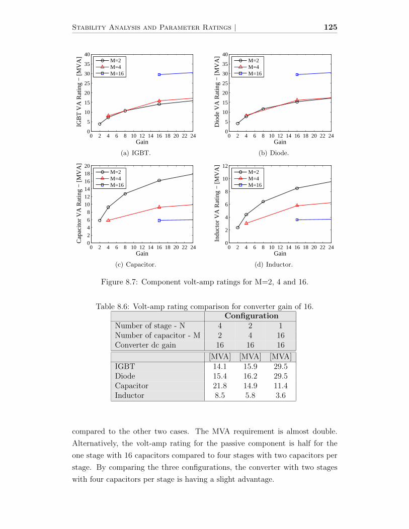
Stability Analysis and Parameter Ratings | 125
0 2 4 6 8 10 12 14 16 18 20 22 240
5
10
15
20
25
30
35
40
Gain
IGB
T V
A R
atin
g −
[MV
A]
M=2M=4M=16
(a) IGBT.
0 2 4 6 8 10 12 14 16 18 20 22 240
5
10
15
20
25
30
35
40
Gain
Dio
de V
A R
atin
g −
[MV
A]
M=2M=4M=16
(b) Diode.
0 2 4 6 8 10 12 14 16 18 20 22 240
2
4
6
8
10
12
14
16
18
20
Gain
Cap
acito
r V
A R
atin
g −
[MV
A]
M=2M=4M=16
(c) Capacitor.
0 2 4 6 8 10 12 14 16 18 20 22 240
2
4
6
8
10
12
Gain
Indu
ctor
VA
Rat
ing
− [M
VA
]
M=2M=4M=16
(d) Inductor.
Figure 8.7: Component volt-amp ratings for M=2, 4 and 16.
Table 8.6: Volt-amp rating comparison for converter gain of 16.Configuration
Number of stage - N 4 2 1Number of capacitor - M 2 4 16Converter dc gain 16 16 16
[MVA] [MVA] [MVA]IGBT 14.1 15.9 29.5Diode 15.4 16.2 29.5Capacitor 21.8 14.9 11.4Inductor 8.5 5.8 3.6
compared to the other two cases. The MVA requirement is almost double.
Alternatively, the volt-amp rating for the passive component is half for the
one stage with 16 capacitors compared to four stages with two capacitors per
stage. By comparing the three configurations, the converter with two stages
with four capacitors per stage is having a slight advantage.

126 Chapter 8 | Marx DC-DC Converter
1 2 3 4 5 6 70
0.5
1
1.5
2
2.5
Number of Stage − N
MV
A/G
ain
IGBTdiode
(a) Power electronics.
1 2 3 4 5 6 70
0.5
1
1.5
2
2.5
3
Number of Stage − N
MV
A/G
ain
capacitorinductor
(b) Passive components.
Figure 8.8: Ratio MVA/Gain for configuration with M=2.
Depending on the relative cost of each component, a weighted factor could
be included in each component calculation so that the best configuration can
be selected for a given converter. Example of factors are the cost of raw
material (i.e. copper), the availability of the components and installation cost
associated with each of them. It is expected that the power electronics will be
the most heavily weighted.
Figure 8.8 evaluates the volt-amp rating as a ratio of the MVA power rat-
ings over the converter gain. The analysis is done for a configuration with
two capacitors per stage (M=2). The advantage of the cascade configura-
tion is shown by having a “MVA cost per gain” decreasing as the number of
stages increases. The ratios are very similar between the power electronics
components. It is different between the passive components with few stages.
However, with seven stages, the ratios for the passive components are almost
the same.
8.2.6 Soft Switching
Each sub-period ends with the inter-stage currents reversing their directions
and being blocked by the inter-stage diodes. Attention is drawn to the fact
after the diodes have blocked, the currents within each stage are all zero. Thus,
the IGBTs, which have been ON, are turned OFF without switching loss. The
next event undergoes lossless switching also: when the IGBTs, which have been
OFF, are turned ON to begin the next sub-period. Therefore, the IGBTs are
operating with zero-current switching.

Stability Analysis and Parameter Ratings | 127
8.3 Chapter Summary
In this chapter, a stability analysis has been performed for the converter op-
erating in both continuous conduction mode and discontinuous conduction
mode. Results have shown that the converter is stable in both modes. In ad-
dition, the power rating of the converter has been estimated. The estimation
evaluates individually the volt-amp ratings of IGBTs, diodes, capacitors and
inductors. The derived equations are valid for a generalized configuration of
a converter with N stages and M capacitors per stage. From this analysis, a
comparison between 3 configurations that produce the same dc voltage gain
has been performed.

128 Chapter 8 | Marx DC-DC Converter

Chapter 9
Marx DC-DC Converter:
Wind Farm Application
In Chapters 5 to 8, the Marx converter has been presented, analyzed and
tested. Its application to an offshore wind farm is introduced in this chapter.
As discussed in the introduction of the thesis (Chapter 1), the need of heavy ac
transformer can be avoided by using a dc collector network instead of an ac bus
in the offshore wind farm. As a result, it reduces the cost of structural support
related to the ac transformer in the offshore platform. The Marx converter is
used to step-up the low dc voltage from the wind turbine converters to the
high dc voltage of the MTDC. The overall wind farm is described and the role
of each part is explained.
A 5MW wind turbine and its ac-dc-dc converter topology are described.
Then, the Marx converter is adapted for wind farm application. The operation
of the receiving-end VSC is briefly explained. Finally, a 200MW offshore wind
farm connected to an onshore VSC station via the Marx converter is simulated
to demonstrate the operation of such system.
9.1 System Description
The configuration of the wind farm with the Marx converter is shown in Figure
9.1. Wind farms are unidirectional power generators and, therefore, they do
not require bidirectional VSC-HVDC station to service them. Furthermore,
as much wind power as can be captured by maximum peak power tracking
(MPPT) is outputted by each wind turbine. The unregulated power from
each wind turbine is summed at the input of the Marx offshore station which
129
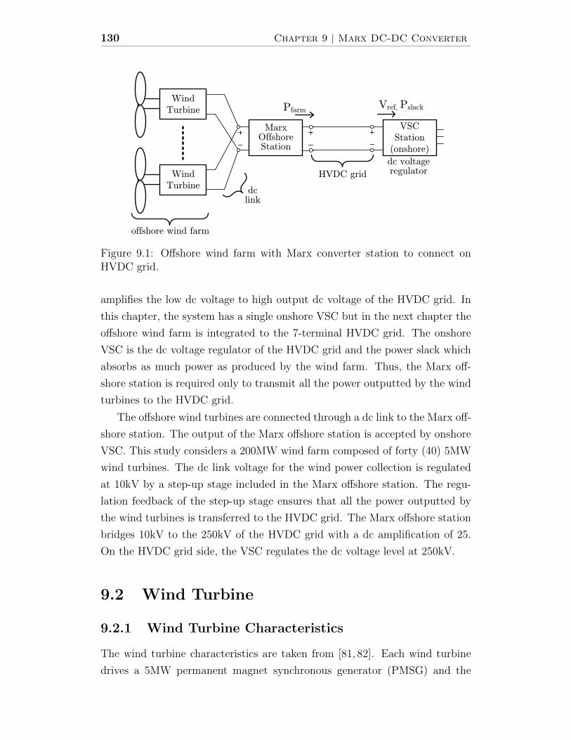
130 Chapter 9 | Marx DC-DC Converter
WindTurbine
WindTurbine
MarxOffshoreStation
dclink
VSCStation(onshore)
HVDC grid
offshore wind farm
Pfarm Vref, Pslack
dc voltageregulator
Figure 9.1: Offshore wind farm with Marx converter station to connect onHVDC grid.
amplifies the low dc voltage to high output dc voltage of the HVDC grid. In
this chapter, the system has a single onshore VSC but in the next chapter the
offshore wind farm is integrated to the 7-terminal HVDC grid. The onshore
VSC is the dc voltage regulator of the HVDC grid and the power slack which
absorbs as much power as produced by the wind farm. Thus, the Marx off-
shore station is required only to transmit all the power outputted by the wind
turbines to the HVDC grid.
The offshore wind turbines are connected through a dc link to the Marx off-
shore station. The output of the Marx offshore station is accepted by onshore
VSC. This study considers a 200MW wind farm composed of forty (40) 5MW
wind turbines. The dc link voltage for the wind power collection is regulated
at 10kV by a step-up stage included in the Marx offshore station. The regu-
lation feedback of the step-up stage ensures that all the power outputted by
the wind turbines is transferred to the HVDC grid. The Marx offshore station
bridges 10kV to the 250kV of the HVDC grid with a dc amplification of 25.
On the HVDC grid side, the VSC regulates the dc voltage level at 250kV.
9.2 Wind Turbine
9.2.1 Wind Turbine Characteristics
The wind turbine characteristics are taken from [81, 82]. Each wind turbine
drives a 5MW permanent magnet synchronous generator (PMSG) and the

Wind Farm Application | 131
Table 9.1: Wind turbine and generator parametersWind Turbine
Rated power [MW] 5Rated wind speed [m/s] 12Cut-in wind speed [m/s] 3Rated shaft speed [rad/s] 1.55Rated frequency [Hz] 35.77Rated torque [Nm] 3.226×10⁶
Rotor and turbine inertia J (2.55sec) 1.06×10⁷
GeneratorInduced voltage EPM [kV RMS
LN ] 2.89Synchronous inductance LS [mH] 6.77
0.5 1 1.5 20
1
2
3
4
5
Hub Speed ωm
− [rad/s]
Pow
er −
[MW
]
10 m/s
11 m/s
12 m/s
Ppeak
(a) Power with peak power identified.
0.5 1 1.5 20
0.5
1
1.5
2
2.5
3
3.5
Hub Speed ωm
− [rad/s]
Tor
que
− [1
06 Nm
]
11 m/s
12 m/s
10 m/s
Topt
(b) Torque with optimal torque curve.
Figure 9.2: Wind turbine characteristic curves for fix pitch angle (β = 0).
main parameters are listed in Table 9.1. The wind turbine power and torque
characteristics for various wind speeds are shown in Figure 9.2. The optimal
torque curve T opt for MPPT is also shown in Figure 9.2(b).
The wind turbine converter, shown in Figure 9.3, is composed of a diode
rectifier to rectify the variable frequency ac generated power from the PMSG
to dc. The diode rectifier is robust and not expensive. The control of the
PMSG is performed by the attached step-up (boost) converter [83]. The step-
up converter regulates the current IDR at the output of the diode rectifier
which has a direct relationship with the ac current on the PMSG. By doing
so, the torque of the machine can be regulated to operate at MPPT.

132 Chapter 9 | Marx DC-DC Converter
EPM LS
Vt
It
PMSG Diode Rectifier Step-Up Converter
VDC
+
-
LUP
+
-VOUT
CDC
IDR
IOUT
+-
+
-
+
-
COUT
LW
Figure 9.3: Wind turbine converter.
The mechanical dynamics of the wind turbine are modeled using first order
Equation (9.1). The objective is to regulate the generator electrical torque Te
such that it follows the optimal torque curve T opt given in Figure 9.2(b) for a
given hub speed ωm.
Jdωmdt
= Tm − Te (9.1)
A set of equations needs to be derived in order to operate the wind turbine
as expected with the step-up converter. The induced voltage by the PMSG is
directly proportional to the mechanical speed ωm and the stator field constant
kPM as given in Equation (9.2).
EPM = kPMωm (9.2)
Similarly, the electrical frequency ωe of the PMSG varies with respect to the
mechanical speed ωm and the relationship is:
ωe =P
2ωm (9.3)
where P is the pole number. The electrical torque of the PMSG is calculated
using:
Te =Peωm
(9.4)
where Pe is the electrical power defined as:
Pe = 3EPMIt cosψ (9.5)
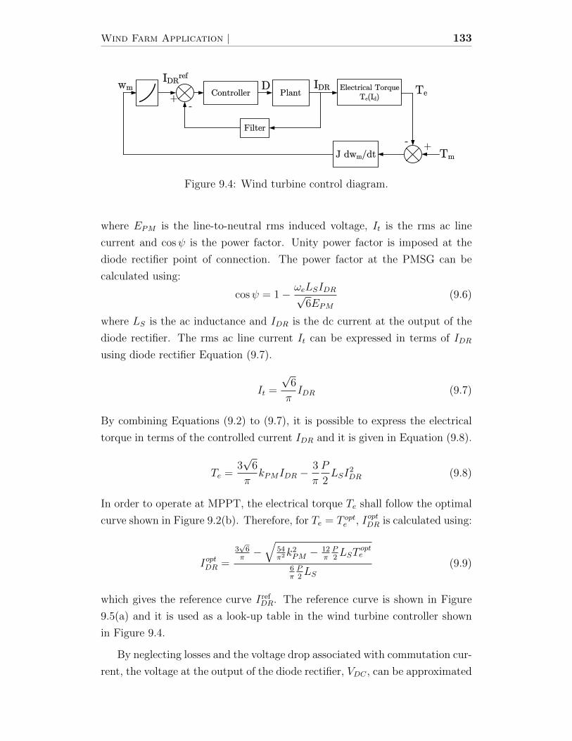
Wind Farm Application | 133
IDRref
PlantIDR
Filter
+-
wm Electrical TorqueTe(Id)
TeController
+-
TmJ dwm/dt
D
Figure 9.4: Wind turbine control diagram.
where EPM is the line-to-neutral rms induced voltage, It is the rms ac line
current and cosψ is the power factor. Unity power factor is imposed at the
diode rectifier point of connection. The power factor at the PMSG can be
calculated using:
cosψ = 1− ωeLSIDR√6EPM
(9.6)
where LS is the ac inductance and IDR is the dc current at the output of the
diode rectifier. The rms ac line current It can be expressed in terms of IDR
using diode rectifier Equation (9.7).
It =
√6
πIDR (9.7)
By combining Equations (9.2) to (9.7), it is possible to express the electrical
torque in terms of the controlled current IDR and it is given in Equation (9.8).
Te =3√
6
πkPMIDR −
3
π
P
2LSI
2DR (9.8)
In order to operate at MPPT, the electrical torque Te shall follow the optimal
curve shown in Figure 9.2(b). Therefore, for Te = T opte , IoptDR is calculated using:
IoptDR =
3√
6π−√
54π2k2
PM − 12πP2LST
opte
6πP2LS
(9.9)
which gives the reference curve IrefDR. The reference curve is shown in Figure
9.5(a) and it is used as a look-up table in the wind turbine controller shown
in Figure 9.4.
By neglecting losses and the voltage drop associated with commutation cur-
rent, the voltage at the output of the diode rectifier, VDC , can be approximated
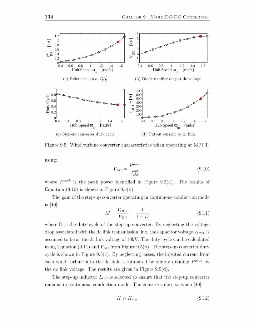
134 Chapter 9 | Marx DC-DC Converter
0.4 0.6 0.8 1 1.2 1.4 1.60
0.20.40.60.8
11.2
Hub Speed ωm
− [rad/s]
I DR
ref −
[kA
]
(a) Reference curve IrefDR .
0.4 0.6 0.8 1 1.2 1.4 1.60123456
Hub Speed ωm
− [rad/s]
VD
C −
[kV
]
(b) Diode rectifier output dc voltage.
0.4 0.6 0.8 1 1.2 1.4 1.60
0.2
0.4
0.6
0.8
1
Hub Speed ωm
− [rad/s]
Dut
y C
ycle
(c) Step-up converter duty cycle.
0.4 0.6 0.8 1 1.2 1.4 1.60
100200300400500600700
Hub Speed ωm
− [rad/s]I O
UT −
[A]
(d) Output current to dc link.
Figure 9.5: Wind turbine converter characteristics when operating at MPPT.
using:
VDC =P peak
IoptDR
(9.10)
where P peak is the peak power identified in Figure 9.2(a). The results of
Equation (9.10) is shown in Figure 9.5(b).
The gain of the step-up converter operating in continuous conduction mode
is [40]:
M =VOUTVDC
=1
1−D(9.11)
where D is the duty cycle of the step-up converter. By neglecting the voltage
drop associated with the dc link transmission line, the capacitor voltage VOUT is
assumed to be at the dc link voltage of 10kV. The duty cycle can be calculated
using Equation (9.11) and VDC from Figure 9.5(b). The step-up converter duty
cycle is shown in Figure 9.5(c). By neglecting losses, the injected current from
each wind turbine into the dc link is estimated by simply dividing P peak by
the dc link voltage. The results are given in Figure 9.5(d).
The step-up inductor LUP is selected to ensure that the step-up converter
remains in continuous conduction mode. The converter does so when [40]:
K > Kcrit (9.12)

Wind Farm Application | 135
0.4 0.6 0.8 1 1.2 1.4 1.60
1
2
3
4
5
6
7
8
Hub Speed ωm
− [rad/s]
Indu
ctor
LU
P − [m
H]
DCM
CCM
Figure 9.6: Wind turbine converter boundary for continuous conduction mode(CCM) and discontinuous conduction mode (DCM).
where
K =2LUPROUTTS
(9.13)
and
Kcrit = D(1−D)2 (9.14)
The inductor value has to be large enough such that Equation (9.12) is satisfied
at low power (cut-in wind speed) as well as high power (rated wind speed). In
Equation (9.13), the resistance ROUT is calculated using:
ROUT =P peak
V 2link
(9.15)
By combining Equations (9.12) to (9.15), the requirement for the inductor LUP
becomes:
LUP >1
2ROUTTSD(1−D)2 (9.16)
The boundary is drawn in Figure 9.6 for the switching frequency of 2kHz
(Ts = 500µs). From the figure, an inductor value of 8uH will ensure operation
in continuous conduction mode in all range of operation of the wind turbine.
The parameters for the wind turbine converter is given in Table 9.2. The
components of the wind turbine converter are selected to ensure adequate
performance of the unit with low voltage ripple on the capacitor.
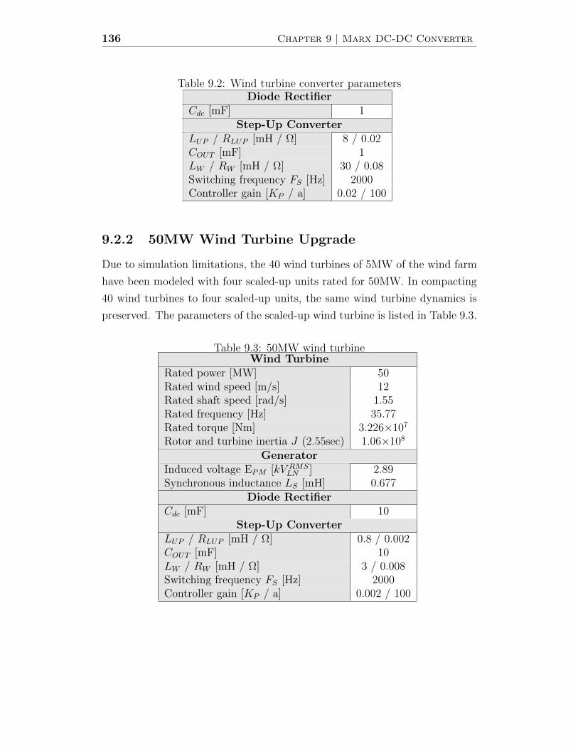
136 Chapter 9 | Marx DC-DC Converter
Table 9.2: Wind turbine converter parametersDiode Rectifier
Cdc [mF] 1Step-Up Converter
LUP / RLUP [mH / Ω] 8 / 0.02COUT [mF] 1LW / RW [mH / Ω] 30 / 0.08Switching frequency FS [Hz] 2000Controller gain [KP / a] 0.02 / 100
9.2.2 50MW Wind Turbine Upgrade
Due to simulation limitations, the 40 wind turbines of 5MW of the wind farm
have been modeled with four scaled-up units rated for 50MW. In compacting
40 wind turbines to four scaled-up units, the same wind turbine dynamics is
preserved. The parameters of the scaled-up wind turbine is listed in Table 9.3.
Table 9.3: 50MW wind turbineWind Turbine
Rated power [MW] 50Rated wind speed [m/s] 12Rated shaft speed [rad/s] 1.55Rated frequency [Hz] 35.77Rated torque [Nm] 3.226×10⁷
Rotor and turbine inertia J (2.55sec) 1.06×10⁸
GeneratorInduced voltage EPM [kV RMS
LN ] 2.89Synchronous inductance LS [mH] 0.677
Diode RectifierCdc [mF] 10
Step-Up ConverterLUP / RLUP [mH / Ω] 0.8 / 0.002COUT [mF] 10LW / RW [mH / Ω] 3 / 0.008Switching frequency FS [Hz] 2000Controller gain [KP / a] 0.002 / 100
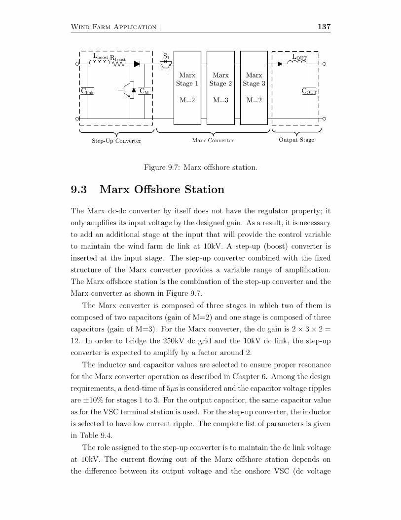
Wind Farm Application | 137
S1
Clink
Lboost Rboost
CM COUT
LOUT
Marx
Stage 1
M=2
Marx
Stage 2
M=3
Marx
Stage 3
M=2
Step-Up Converter Marx Converter Output Stage
Figure 9.7: Marx offshore station.
9.3 Marx Offshore Station
The Marx dc-dc converter by itself does not have the regulator property; it
only amplifies its input voltage by the designed gain. As a result, it is necessary
to add an additional stage at the input that will provide the control variable
to maintain the wind farm dc link at 10kV. A step-up (boost) converter is
inserted at the input stage. The step-up converter combined with the fixed
structure of the Marx converter provides a variable range of amplification.
The Marx offshore station is the combination of the step-up converter and the
Marx converter as shown in Figure 9.7.
The Marx converter is composed of three stages in which two of them is
composed of two capacitors (gain of M=2) and one stage is composed of three
capacitors (gain of M=3). For the Marx converter, the dc gain is 2× 3× 2 =
12. In order to bridge the 250kV dc grid and the 10kV dc link, the step-up
converter is expected to amplify by a factor around 2.
The inductor and capacitor values are selected to ensure proper resonance
for the Marx converter operation as described in Chapter 6. Among the design
requirements, a dead-time of 5µs is considered and the capacitor voltage ripples
are ±10% for stages 1 to 3. For the output capacitor, the same capacitor value
as for the VSC terminal station is used. For the step-up converter, the inductor
is selected to have low current ripple. The complete list of parameters is given
in Table 9.4.
The role assigned to the step-up converter is to maintain the dc link voltage
at 10kV. The current flowing out of the Marx offshore station depends on
the difference between its output voltage and the onshore VSC (dc voltage

138 Chapter 9 | Marx DC-DC Converter
Table 9.4: Marx offshore station parametersInput reactor [mH / Ω] 1.2 / 0.02
Step-Up ConverterClink [mF] 40Lboost / Rboost [mH / Ω] 2 / 0.02CM [mF] 10Switching frequency FS [kHz] 2Controller gain [KP / a] 0.005 / 150
Marx ConverterNumber of stages 3Number of steps M1, M2, M3, 2, 3, 2Switching frequency - fsw [kHz] 2Dead-time - tdead [µs] 5L1 / RL1 [uH / Ω] 5 / 0.01C1 [uF] 625L2 / RL2 [uH / Ω] 38.5 / 0.01C2 [uF] 105L3 / RL3 [uH / Ω] 342.5 / 0.01C3 [uF] 18LOUT / RLOUT [uH / Ω] 684.5 / 0.01COUT [mF] 0.4Output reactor Lreac [mH / Ω] 2 / 0.02
regulator). If the step-up converter increases its amplification, the output
voltage of the Marx offshore station increases which results in higher power
outputted.
When more power is produced by the wind turbines, the increased output
currents from the wind turbines charge the dc link capacitor to a voltage higher
than 10kV. From the schematic of Figure 9.8, the step-up converter control
adjusts the duty cycle D to increase the output voltage of the step-up converter
which is the input voltage of the Marx converter and thereby increase the dc
power outputted into the HVDC link. When the power outputted by the Marx
offshore station is equal to the power outputted by the wind farm, the 10kV
is regulated.
9.4 VSC Terminal Station
The VSC terminal station at the receiving end has the same parameter as
terminal station T2 used in the simulations of Chapter 4. From the dq-axis

Wind Farm Application | 139
Vlinkref=10kV PI
Controller
Vlinkmeas
D
Filter
-1
Figure 9.8: Control diagram of the step-up converter included in the Marxoffshore station.
controller, the d-axis control is applied in negative feedback to regulate the dc
voltage at Vref which is set to 250kV. The parameters can be found in Table
C.3 of Appendix C.
9.5 Simulation Results
The system of Figure 9.1 has been simulated in the PSCAD-EMTDC software
package, an industry-grade software for high voltage power electronic research.
It is composed of a 200MW offshore wind farm modeled with 4 scaled-up wind
turbines (50MW each), the Marx offshore station and the onshore VSC station.
The transmission line parameters are given in Table 9.5.
In the beginning of the simulation, the wind turbines are operating at rated
wind speed of 12m/s. Figure 9.9(a) shows their respective wind speeds and
output power PWT . Figure 9.9(b) shows the total wind power from the Marx
offshore station received by the onshore VSC station. The lower graph shows
the voltage at the terminal of the VSC station with the regulator reference set
at 250kV.
Then, the wind speed decreases to different values for each wind turbine.
The power produced by the wind turbines decreases also and the total power
injected in the dc grid changes from 200MW to 52MW. The average voltage
in steady-state at the Marx offshore station is listed in Table 9.6. The dc link
Table 9.5: Transmission line parametersDistance Resistance Inductance
[km] [Ω] [mH]Wind Turbine (50MW) to 1 0.0012 0.0106Marx offshore stationMarx offshore station to 413 5 44onshore VSC station
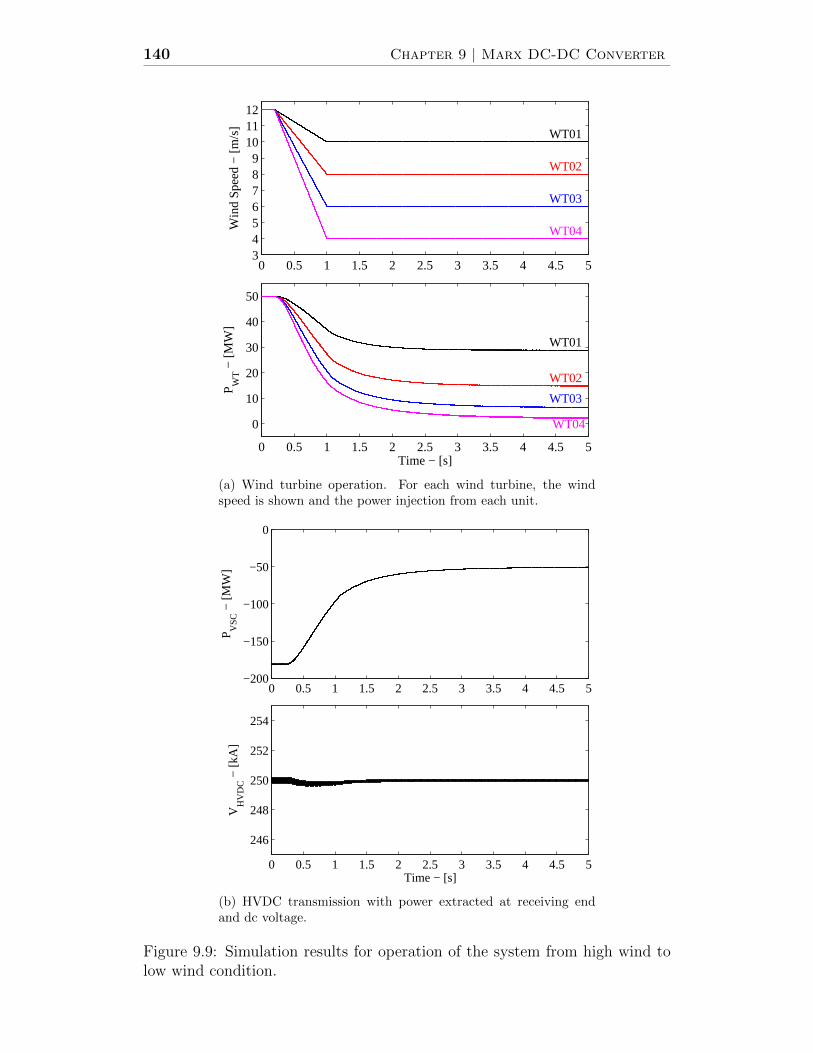
140 Chapter 9 | Marx DC-DC Converter
0 0.5 1 1.5 2 2.5 3 3.5 4 4.5 53456789
101112
Win
d S
peed
− [m
/s]
WT01
WT02
WT03
WT04
0 0.5 1 1.5 2 2.5 3 3.5 4 4.5 5
0
10
20
30
40
50
P WT −
[MW
]
WT01
WT02
WT03
WT04
Time − [s]
(a) Wind turbine operation. For each wind turbine, the windspeed is shown and the power injection from each unit.
0 0.5 1 1.5 2 2.5 3 3.5 4 4.5 5−200
−150
−100
−50
0
P VS
C −
[MW
]
0 0.5 1 1.5 2 2.5 3 3.5 4 4.5 5
246
248
250
252
254
VH
VD
C −
[kA
]
Time − [s]
(b) HVDC transmission with power extracted at receiving endand dc voltage.
Figure 9.9: Simulation results for operation of the system from high wind tolow wind condition.
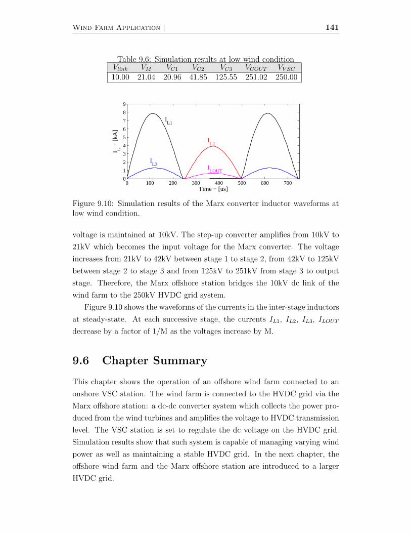
Wind Farm Application | 141
Table 9.6: Simulation results at low wind conditionVlink VM VC1 VC2 VC3 VCOUT VV SC10.00 21.04 20.96 41.85 125.55 251.02 250.00
0 100 200 300 400 500 600 7000
1
2
3
4
5
6
7
8
9
I L −
[kA
]IL1
IL2
IL3
ILOUT
Time − [us]
Figure 9.10: Simulation results of the Marx converter inductor waveforms atlow wind condition.
voltage is maintained at 10kV. The step-up converter amplifies from 10kV to
21kV which becomes the input voltage for the Marx converter. The voltage
increases from 21kV to 42kV between stage 1 to stage 2, from 42kV to 125kV
between stage 2 to stage 3 and from 125kV to 251kV from stage 3 to output
stage. Therefore, the Marx offshore station bridges the 10kV dc link of the
wind farm to the 250kV HVDC grid system.
Figure 9.10 shows the waveforms of the currents in the inter-stage inductors
at steady-state. At each successive stage, the currents IL1, IL2, IL3, ILOUT
decrease by a factor of 1/M as the voltages increase by M.
9.6 Chapter Summary
This chapter shows the operation of an offshore wind farm connected to an
onshore VSC station. The wind farm is connected to the HVDC grid via the
Marx offshore station: a dc-dc converter system which collects the power pro-
duced from the wind turbines and amplifies the voltage to HVDC transmission
level. The VSC station is set to regulate the dc voltage on the HVDC grid.
Simulation results show that such system is capable of managing varying wind
power as well as maintaining a stable HVDC grid. In the next chapter, the
offshore wind farm and the Marx offshore station are introduced to a larger
HVDC grid.

142 Chapter 9 | Marx DC-DC Converter

Part III
Complete Multiterminal HVDC
System
143

144
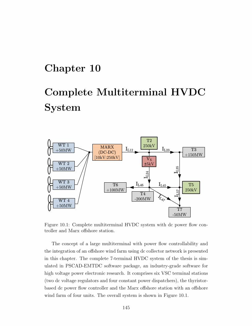
Chapter 10
Complete Multiterminal HVDC
System
T2250kV
T4-200MW
T6+100MW
T3+150MW
T5250kV
T7-50MW
IL12 IL23I L24 I L35
IL45IL46
I L57
IL47
WT 1+50MW
WT 2+50MW
WT 3+50MW
WT 4+50MW
VX±5kV
MARX(DC-DC)
[10kV:250kV]
Figure 10.1: Complete multiterminal HVDC system with dc power flow con-troller and Marx offshore station.
The concept of a large multiterminal with power flow controllability and
the integration of an offshore wind farm using dc collector network is presented
in this chapter. The complete 7-terminal HVDC system of the thesis is sim-
ulated in PSCAD-EMTDC software package, an industry-grade software for
high voltage power electronic research. It comprises six VSC terminal stations
(two dc voltage regulators and four constant power dispatchers), the thyristor-
based dc power flow controller and the Marx offshore station with an offshore
wind farm of four units. The overall system is shown in Figure 10.1.
145
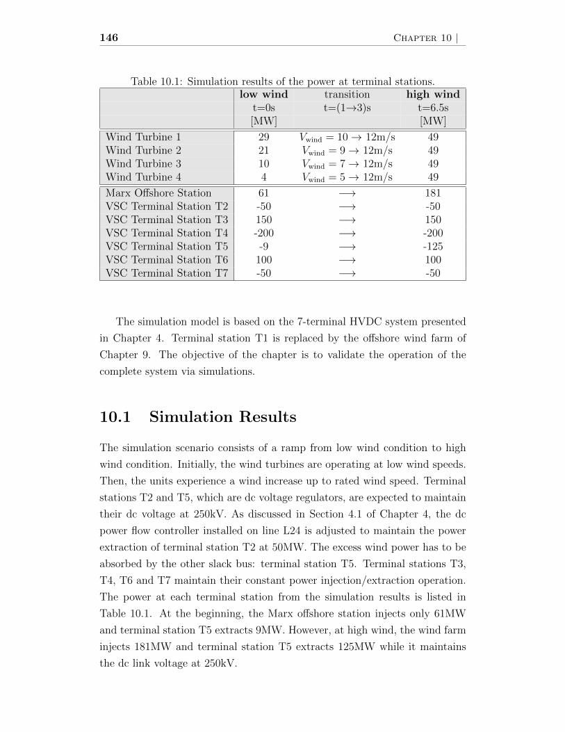
146 Chapter 10 |
Table 10.1: Simulation results of the power at terminal stations.low wind transition high wind
t=0s t=(1→3)s t=6.5s[MW] [MW]
Wind Turbine 1 29 Vwind = 10→ 12m/s 49Wind Turbine 2 21 Vwind = 9→ 12m/s 49Wind Turbine 3 10 Vwind = 7→ 12m/s 49Wind Turbine 4 4 Vwind = 5→ 12m/s 49
Marx Offshore Station 61 −→ 181VSC Terminal Station T2 -50 −→ -50VSC Terminal Station T3 150 −→ 150VSC Terminal Station T4 -200 −→ -200VSC Terminal Station T5 -9 −→ -125VSC Terminal Station T6 100 −→ 100VSC Terminal Station T7 -50 −→ -50
The simulation model is based on the 7-terminal HVDC system presented
in Chapter 4. Terminal station T1 is replaced by the offshore wind farm of
Chapter 9. The objective of the chapter is to validate the operation of the
complete system via simulations.
10.1 Simulation Results
The simulation scenario consists of a ramp from low wind condition to high
wind condition. Initially, the wind turbines are operating at low wind speeds.
Then, the units experience a wind increase up to rated wind speed. Terminal
stations T2 and T5, which are dc voltage regulators, are expected to maintain
their dc voltage at 250kV. As discussed in Section 4.1 of Chapter 4, the dc
power flow controller installed on line L24 is adjusted to maintain the power
extraction of terminal station T2 at 50MW. The excess wind power has to be
absorbed by the other slack bus: terminal station T5. Terminal stations T3,
T4, T6 and T7 maintain their constant power injection/extraction operation.
The power at each terminal station from the simulation results is listed in
Table 10.1. At the beginning, the Marx offshore station injects only 61MW
and terminal station T5 extracts 9MW. However, at high wind, the wind farm
injects 181MW and terminal station T5 extracts 125MW while it maintains
the dc link voltage at 250kV.
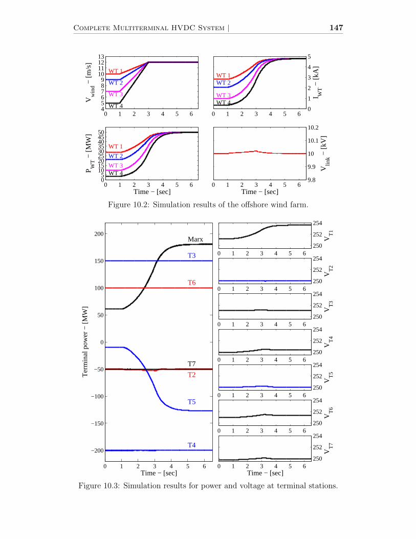
Complete Multiterminal HVDC System | 147
0 1 2 3 4 5 6456789
10111213
Vw
ind −
[m/s
]
WT 1
WT 2
WT 3
WT 40 1 2 3 4 5 6
0
1
2
3
4
5
I WT −
[kA
]
WT 1WT 2
WT 3WT 4
0 1 2 3 4 5 605
101520253035404550
P WT −
[MW
]
Time − [sec]
WT 1
WT 2
WT 3WT 4
0 1 2 3 4 5 69.8
9.9
10
10.1
10.2
Vlin
k − [k
V]
Time − [sec]
Figure 10.2: Simulation results of the offshore wind farm.
0 1 2 3 4 5 6
−200
−150
−100
−50
0
50
100
150
200
Ter
min
al p
ower
− [M
W]
Time − [sec]
Marx
T3
T6
T7
T2
T5
T4
0 1 2 3 4 5 6250
252
254
VT
1
0 1 2 3 4 5 6250
252
254
VT
20 1 2 3 4 5 6
250
252
254
VT
3
0 1 2 3 4 5 6250
252
254V
T4
0 1 2 3 4 5 6250
252
254
VT
5
0 1 2 3 4 5 6250
252
254
VT
6
0 1 2 3 4 5 6250
252
254
VT
7
Time − [sec]
Figure 10.3: Simulation results for power and voltage at terminal stations.

148 Chapter 10 |
The simulation results for the wind turbines are shown in Figure 10.2.
Initially, wind turbines operate at different wind speed. The current IWT
injected by each wind turbine into the 10kV dc link depends on their power
production. Then, the wind speeds increase so that all wind turbines operate
at rated wind speed after the transition. As shown in Figure 10.2, the increase
is smooth and the wind turbines remain stable. The Marx offshore station is
capable of maintaining the dc link voltage at 10kV. A slight increase in the dc
link voltage is observed during the transition but it resumes rapidly.
Figure 10.3 gives a good overview of the operation of the MTDC by show-
ing the power at each terminal station and their respective terminal voltages.
Positive power represents injection into the MTDC and negative power is asso-
ciated with power extraction from the MTDC. The powers remain constant for
all terminal stations except for the Marx offshore station and terminal station
T5. The power injected by the Marx offshore station increases as the wind
farm produces more power; the Marx offshore station links the wind farm and
the HVDC grid. Without the dc power flow controller, the increasing wind
power would have been distributed among the two slack buses terminal stations
T2 and T5. However, with the dc power flow controller, the power extracted
by terminal station T2 is maintained at 50MW and terminal station T5 is
extracting the rest of the injected wind power. The dc power flow controller
succeeds in diverting the power from terminal station T2 to terminal station
T5. The terminal voltages are shown to remain stable and terminal stations
T2 and T5 regulate the HVDC grid voltage at 250kV.
The transmission line currents are shown in Figure 10.4 and the power flow
pattern can be interpreted. Most of the excess power produced by the wind
farm is transmitted through path L24-L45 instead of L23-L35. The current in
transmission line L45 changes direction as the wind power increases. Line L24
has more ripple and it comes from the harmonics created by the dc power flow
controller as studied in Chapter 3. The transmission line currents for low wind
and high wind conditions are shown in Table 10.2. The table also includes the
power transmitted through each line and the changes are indicated with ↑ or
↓. Within the eight transmission line currents, four are increasing, three do
not vary and one is decreasing.
The response of the dc power flow controller is shown in Figure 10.5. The
reference for the outer loop controller is the power of terminal station T2 at
−50MW. During the transition, there is a decrease by 3MW but it resumes
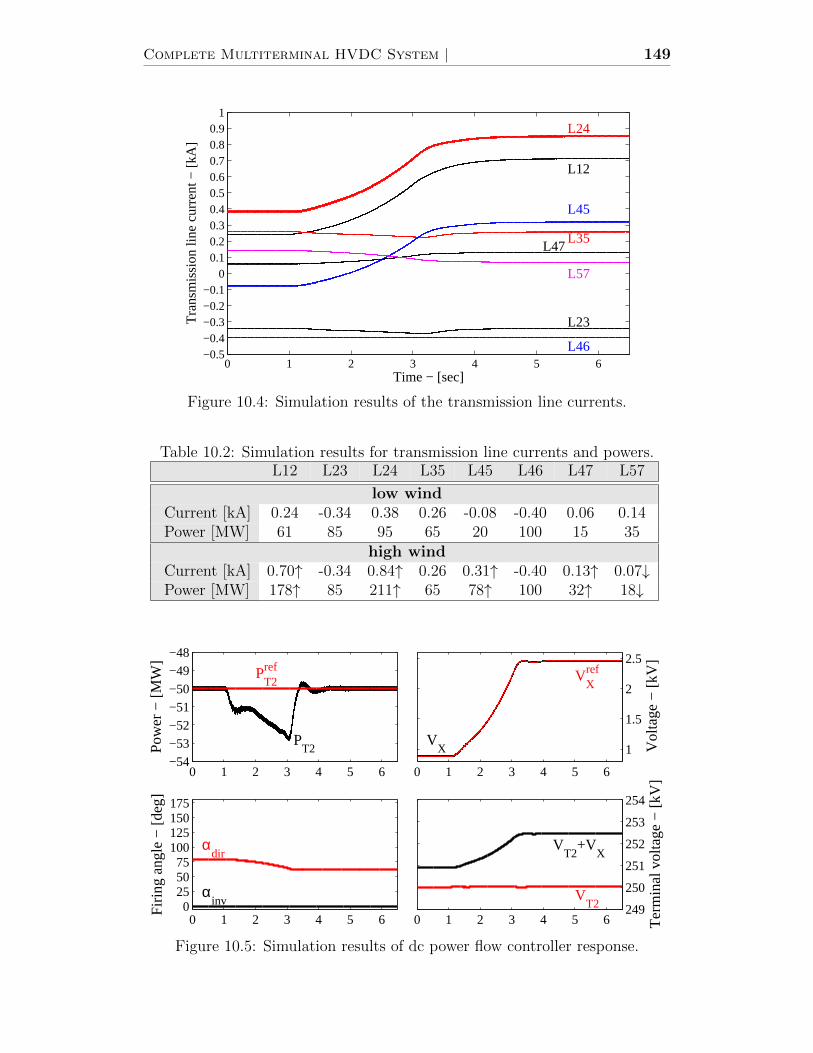
Complete Multiterminal HVDC System | 149
0 1 2 3 4 5 6−0.5−0.4−0.3−0.2−0.1
00.10.20.30.40.50.60.70.80.9
1
Tra
nsm
issi
on li
ne c
urre
nt −
[kA
]
Time − [sec]
L24
L12
L45
L35L47
L57
L23
L46
Figure 10.4: Simulation results of the transmission line currents.
Table 10.2: Simulation results for transmission line currents and powers.L12 L23 L24 L35 L45 L46 L47 L57
low windCurrent [kA] 0.24 -0.34 0.38 0.26 -0.08 -0.40 0.06 0.14Power [MW] 61 85 95 65 20 100 15 35
high windCurrent [kA] 0.70↑ -0.34 0.84↑ 0.26 0.31↑ -0.40 0.13↑ 0.07↓Power [MW] 178↑ 85 211↑ 65 78↑ 100 32↑ 18↓
0 1 2 3 4 5 6−54
−53
−52
−51
−50
−49
−48
Pow
er −
[MW
]
PT2ref
PT2
0 1 2 3 4 5 6
1
1.5
2
2.5V
olta
ge −
[kV
]
VX
VXref
0 1 2 3 4 5 60
255075
100125150175
Firi
ng a
ngle
− [d
eg]
αinv
αdir
0 1 2 3 4 5 6249
250
251
252
253
254
Ter
min
al v
olta
ge −
[kV
]
VT2
+VX
VT2
Figure 10.5: Simulation results of dc power flow controller response.
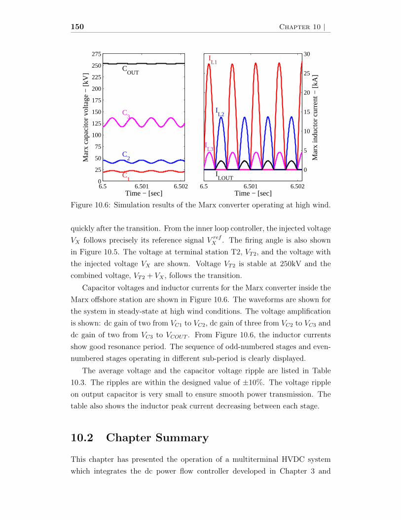
150 Chapter 10 |
6.5 6.501 6.5020
25
50
75
100
125
150
175
200
225
250
275
Mar
x ca
paci
tor
volta
ge −
[kV
]
Time − [sec]
COUT
C3
C2
C1
6.5 6.501 6.502
0
5
10
15
20
25
30
Mar
x in
duct
or c
urre
nt −
[kA
]
Time − [sec]
IL1
IL2
IL3
ILOUT
Figure 10.6: Simulation results of the Marx converter operating at high wind.
quickly after the transition. From the inner loop controller, the injected voltage
VX follows precisely its reference signal V refX . The firing angle is also shown
in Figure 10.5. The voltage at terminal station T2, VT2, and the voltage with
the injected voltage VX are shown. Voltage VT2 is stable at 250kV and the
combined voltage, VT2 + VX , follows the transition.
Capacitor voltages and inductor currents for the Marx converter inside the
Marx offshore station are shown in Figure 10.6. The waveforms are shown for
the system in steady-state at high wind conditions. The voltage amplification
is shown: dc gain of two from VC1 to VC2, dc gain of three from VC2 to VC3 and
dc gain of two from VC3 to VCOUT . From Figure 10.6, the inductor currents
show good resonance period. The sequence of odd-numbered stages and even-
numbered stages operating in different sub-period is clearly displayed.
The average voltage and the capacitor voltage ripple are listed in Table
10.3. The ripples are within the designed value of ±10%. The voltage ripple
on output capacitor is very small to ensure smooth power transmission. The
table also shows the inductor peak current decreasing between each stage.
10.2 Chapter Summary
This chapter has presented the operation of a multiterminal HVDC system
which integrates the dc power flow controller developed in Chapter 3 and
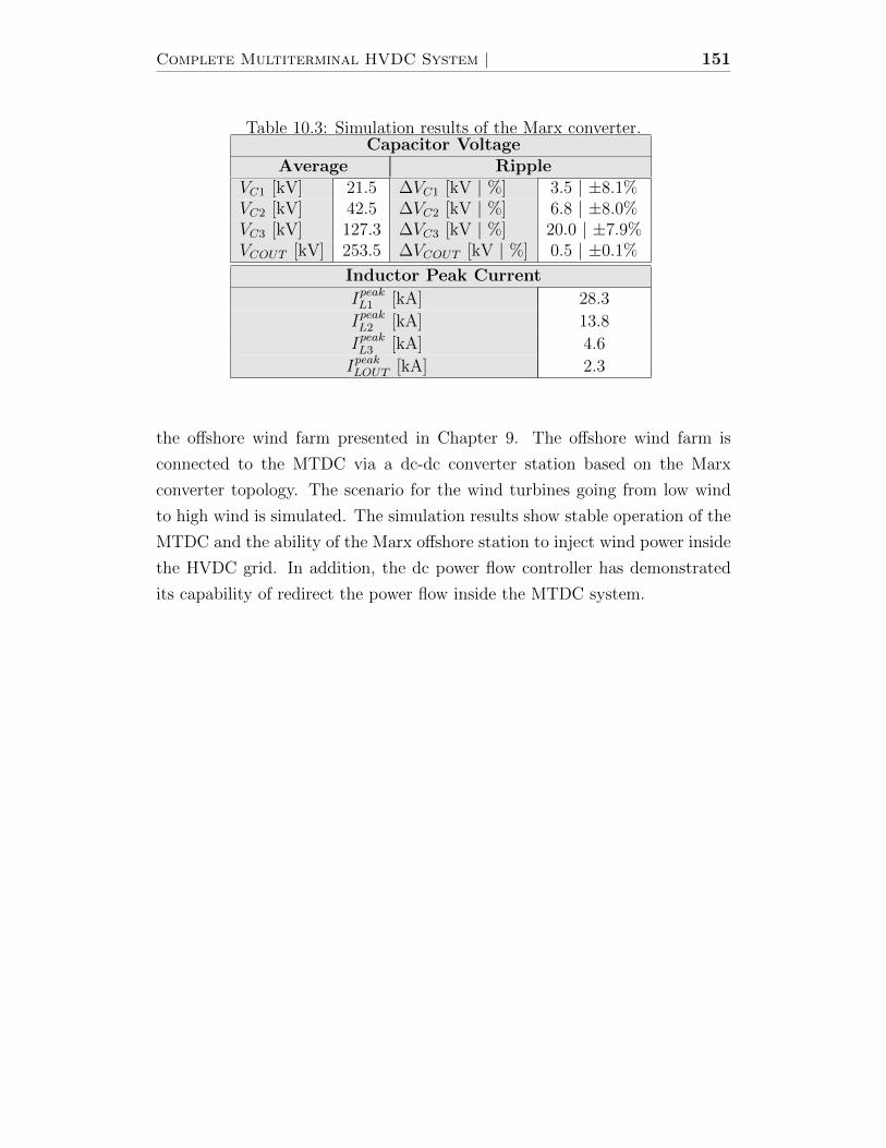
Complete Multiterminal HVDC System | 151
Table 10.3: Simulation results of the Marx converter.Capacitor Voltage
Average RippleVC1 [kV] 21.5 ∆VC1 [kV | %] 3.5 | ±8.1%VC2 [kV] 42.5 ∆VC2 [kV | %] 6.8 | ±8.0%VC3 [kV] 127.3 ∆VC3 [kV | %] 20.0 | ±7.9%VCOUT [kV] 253.5 ∆VCOUT [kV | %] 0.5 | ±0.1%
Inductor Peak Current
IpeakL1 [kA] 28.3
IpeakL2 [kA] 13.8
IpeakL3 [kA] 4.6
IpeakLOUT [kA] 2.3
the offshore wind farm presented in Chapter 9. The offshore wind farm is
connected to the MTDC via a dc-dc converter station based on the Marx
converter topology. The scenario for the wind turbines going from low wind
to high wind is simulated. The simulation results show stable operation of the
MTDC and the ability of the Marx offshore station to inject wind power inside
the HVDC grid. In addition, the dc power flow controller has demonstrated
its capability of redirect the power flow inside the MTDC system.

152 Chapter 10 |

Chapter 11
Conclusion
11.1 Thesis Summary
This thesis has introduced the concept of the dc power flow controller inside
a HVDC grid to address the power flow control issue. It consists of inserting
on a dc transmission line a device in series that varies the dc voltage on that
specific line. By doing so, the transmission line current can be adjusted and
the power flow varied. Because the dc line resistance is small, the inserted
voltage variation does not have to be large.
Before proceeding to realizing the dc power flow controller, its benefits
to power flow controllability need to be determined first. This is initially
evaluated for a 3-terminal HVDC grid and then for a 4-terminal HVDC grid.
The evaluation shows significant increase in the region of operation for each
system which justifies proceeding to the next phase of hardware realization.
The proposed dc power flow controller consists of two 6-pulse thyristor-
bridges connected in a dual-converter configuration so that it has 4-quadrant
control. It is connected in series on the dc line and it is presented as a small
appendage of a VSC-HVDC station. The thyristor power flow controller has
been simulated in a 3-terminal HVDC grid and it is shown to be fast and stable.
Then, a 7-terminal HVDC grid is presented. The HVDC grid is shown to ben-
efit from having the dc power flow controller to supplement the controllability
of two HVDC stations operating as dc voltage regulators. N-1 contingency for
dc transmission lines is studied and the operation of the system is simulated.
In addition to the dc power flow controller, a new dc-dc converter topology
has been presented. The dc-dc converter is capable of changing the output to
input dc voltage ratio. The topology is based on the Marx generator concept
153

154 Chapter 11 |
of charging capacitors in parallel followed by reconnection in series of the
capacitors to create higher dc voltage. The electric charge transfer is done
via L-C resonance and a diode ensures that the charge transfer of each cycle
is unidirectional. The converter topology can have multiple cascaded stages
to reduce VA requirement in component size while obtaining high dc voltage
amplification. The converter with a configuration of N = 3 stages with M = 3
dc voltage gain per stage, for an overall gain of MN = 33 = 27, is simulated
for proof of concept.
A detailed analysis of the Marx converter topology is presented. The anal-
ysis results in design guidelines intended for proper component sizing. Among
the design requirements, losses and dead-time for switching events are consid-
ered.
From the design, a prototype has been constructed to verify experimentally
the converter topology. The construction has been done gradually with N = 1
stage with dc amplification of M = 2 and subsequently upgraded to N = 2
stages with M = 2. The rating of the prototype converter is 5kW with input
voltage of 110V and a theoretical dc voltage gain of MN = 4. The experimental
work has demonstrated dc voltage amplification and the stable operation of
the converter. Among the tests performed, a load step change has been applied
and operation at different switching frequencies has been tested.
A stability analysis of the topology has been developed based on sampled-
data approach. It evaluates the eigenvalues of the converter operating in con-
tinuous and discontinuous modes. Additionally, parameter ratings are eval-
uated with derived equations. The evaluation covers IGBT switches, diodes,
inductors and capacitors.
The Marx converter is adapted for offshore wind farm application. The
adaptation recognizes that the Marx converter has only a fix dc gain. There-
fore, a boost step-up converter is added in series to give a degree of dc gain
controllability. The combination is given the name “Marx offshore station” in
the thesis.
A software model, composed of a 200MW offshore wind farm, a Marx off-
shore station and an onshore VSC station, has been developed for simulation.
The offshore wind farm is based on wind turbines driving permanent magnet
synchronous generators. Diode rectifiers and boost dc-dc converters aggregate
wind power to a 10kV dc collector network. The Marx offshore station bridges
the 10kV dc link to the 250kV HVDC transmission line. This approach avoids
Conclusion | 155
the high civil engineering cost of an offshore platform capable of supporting
heavy ac transformers which are required for HVDC transmission. Simula-
tion results show stable operation of the wind turbine during wind change
and confirm the Marx offshore station to be capable of bridging the two dc
networks.
Finally, the two parts of the research of this thesis are integrated within a
complete multiterminal HVDC system. It is a 7-terminal HVDC grid which
has a dc power flow controller and an offshore wind farm including the Marx
offshore station. This large multiterminal HVDC system is simulated and each
part developed in this work performs as expected and jointly.
11.2 Conclusions
The research has shown that a dc power flow controller increases the flexibility
and the region of operation of MTDC. The design of the dc power flow con-
troller based on two 6-pulse thyristor-bridges has been proven to be adequate
to the tasks.
Simulation results and the hardware prototype have demonstrated that the
Marx dc-dc converter is capable of high power, high dc voltage operation. The
Marx dc-dc converter is shown to be suitable for offshore wind farm to deliver
wind farm power from its low dc voltage bus to the high dc voltage of the
MTDC grid.
Both the dc power flow controller and the Marx dc-dc converter enlarge
the scope of MTDC.
11.3 Thesis Contributions
The items listed below are original contributions.
11.3.1 DC Power Flow Controller
• The DC Power Flow Controller, as an auxiliary controller of a VSC
station, based on thyristor-based dual-converter. The DC Power Flow
Controller is inserted in a dc transmission line to increase the control-
lability of a dc grid based on multiterminal HVDC. (Chapters 3 and
4)

156 Chapter 11 |
• Apart from the realization of the controller, the research has evaluated
that the controller does increase the feasible region of operation of the
dc grid thus justifying its presence. (Chapter 2)
11.3.2 Marx DC-DC Converter
• The innovative dc-dc converter, which has been adapted from the well
known Marx generator to serve as a continuous high voltage, high power
dc-dc converter. Besides simulation, experimental prototypes have been
constructed and tested for proof of concept. (Chapters 5-7)
• Innovation, which consists of electric charge transfers from the input end
to the output end using L-C resonance with a diode to the inductor to
ensure continuous, unidirectional power transfer. (Chapters 5 and 6)
• Innovation, which consists of design equations for determining the ca-
pacitor size for dc voltage gain M. (Chapter 6)
• Innovation, which consists of applying cascading stages to the Marx dc-dc
converter. As the dc voltage increases in each stage, it has a correspond-
ing current decrease whereby the VA rating is constant at each stage.
(Chapters 5 and 6)
• An innovative method of asymptotic stability analysis based on solving
linear equations x = Ax + Bu in each sub-period of IGBT switching
and integrating the output states at the end of the kth sub-period as
the initial state of the (k+1)th sub-period. Stability is assured when the
eigenvalues are lying within the unit circle in the complex plane. (Section
8.1 of Chapter 8)
• A method of cost evaluation for the choice of N (the number of cascading
stages) and M (the dc voltage gain of each stage) to achieve an overall
dc voltage gain of MN . The method depends on deriving equations
for components based on the voltage and current ratings at each stage.
(Section 8.2 of Chapter 8)

Conclusion | 157
11.4 Future Research
HVDC technology is developing in many directions through technological in-
novation (e.g. MMC) and network expansion (e.g. HVDC grid). Before the
potential of HVDC grid is exploitable, more research has to be done. For ex-
ample, the CIGRE study committee B4 (HVDC and Power Electronics) has
six active Working Bodies to address various issues such as feasibility, control
and protection, design and “grid code” [84].
Regarding the work in this thesis, future research would include:
11.4.1 DC Power Flow Controller
• Consider IGBT and IGCT families of current-source converters.
• Apply the dc power flow controller to the upcoming DC Grid CIGRE
Benchmark model developed by the Working Body B4-52. The latter is
expected to be released soon.
• Study operation of the dc power flow controller under MTDC fault sce-
narios.
• Develop analysis to obtain optimal location of the dc power flow con-
troller inside a MTDC.
• Study the interactions and the benefits of having the interconnection of
two large electrical networks of different technologies (ac and dc). The
situation can be studied from the electrical network stability and the
economical points of view.
11.4.2 Marx DC-DC Converter
• Develop adaptations of the topology for bidirectional capability.
• Study response of the converter with internal and external fault cases.
• Evaluate quantitatively the efficiency of the converter with optimization
tool to minimize losses.
• Study the feasibility for other application such as solar panel.

158 Chapter 11 |

Appendix A
Associated Publications
A.1 Journal Article
• E. Veilleux and B.-T. Ooi, “Multiterminal HVDC with Thyristor Power-
Flow Controller,” IEEE Transactions on Power Delivery, vol. 27, no. 3,
pp. 1205-1212, July 2012.
A.2 Conference Proceedings
• E. Veilleux and B.-T. Ooi, “Multi-Terminal HVDC Grid with Power Flow
Controllability,” in CIGRE 2012 Session, Paris, August 26-31, 2012.
• E. Veilleux and B.-T. Ooi, “Power Flow Analysis in Multi-Terminal
HVDC Grid,” in IEEE PES Power Systems Conference & Exposition,
Phoenix, AZ, USA, March 20-23, 2011.
A.3 Submitted for Publications
• E. Veilleux and B.-T. Ooi, “A DC-DC Converter using Marx Generator
Concept.” Submitted to IEEE Transactions on Power Delivery.
• E. Veilleux, B.-T. Ooi and P. Lehn, “Marx DC-DC Converter for High
Power Application,” Submitted to IET Power Electronics.
• E. Veilleux and B.-T. Ooi, “Marx-dc-dc Converter for Connecting Off-
shore Wind Farms to Multiterminal HVDC,” Submitted to 2013 IEEE
PES General Meeting, Vancouver, BC, Canada, July 21-25, 2013.
159

160 Appendix A | Associated Publications
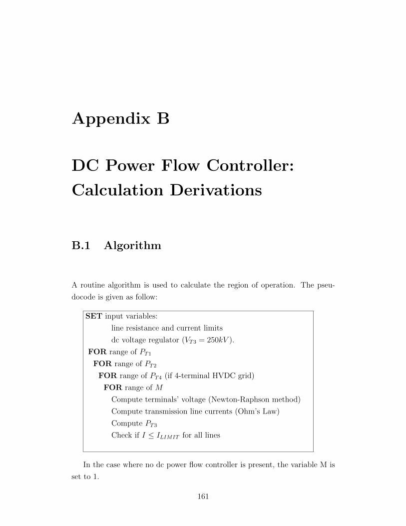
Appendix B
DC Power Flow Controller:
Calculation Derivations
B.1 Algorithm
A routine algorithm is used to calculate the region of operation. The pseu-
docode is given as follow:
SET input variables:
line resistance and current limits
dc voltage regulator (VT3 = 250kV ).
FOR range of PT1
FOR range of PT2
FOR range of PT4 (if 4-terminal HVDC grid)
FOR range of M
Compute terminals’ voltage (Newton-Raphson method)
Compute transmission line currents (Ohm’s Law)
Compute PT3
Check if I ≤ ILIMIT for all lines
In the case where no dc power flow controller is present, the variable M is
set to 1.
161

162 Appendix B | DC Power Flow Controller
B.1.1 Voltage Calculation
The voltages are computed using iterative calculations with the Newton-Raphson
method [85], it is defined as :
VT (i+ 1) = VT (i) + J−1(i)P − P (VT (i))
(B.1)
where VT is the iterative computed terminal voltage, J is the Jacobian matrix,
P is the fix power level and P is the power calculation function.
B.2 Equations for 3-Terminal 3-Line MTDC
The equations for the 3-terminal 3-line system are recalled from Chapter 2.
More precisely, recalling Equations (2.1), (2.2) and (2.7) for the line currents:
IL13 =VT1 − VT3
RL13
(B.2)
IL23 =VT2 − VT3
RL23
(B.3)
IL12 =MVT1 − VT2
RL12
(B.4)
and Equations (2.8) and (2.9) for the terminal powers:
PT1 = V 2T1
[1
RL13
+M2
RL12
]+ VT1
[−VT3
RL13
+MVT2
RL12
](B.5)
PT2 = V 2T2
[1
RL23
+1
RL12
]+ VT2
[−VT3
RL23
+MVT1
RL12
](B.6)
B.2.1 Jacobian Matrix
The Jacobian matrix for the 3-terminal 3-line system is defined as:
J =
[∂PT1/∂VT1 ∂PT1/∂VT2
∂PT2/∂VT1 ∂PT2/∂VT2
](B.7)
where the partial derivatives are derived using Equations (B.5) and (B.6). It
gives:∂PT1
∂VT1
= 2VT1
[1
RL13
+M2
RL12
]+
[−VT3
RL13
+MVT2
RL12
](B.8)

Calculation Derivations | 163
∂PT1
∂VT2
=
[MVT1
RL12
](B.9)
∂PT2
∂VT1
=
[MVT2
RL12
](B.10)
∂PT2
∂VT2
= 2VT2
[1
RL23
+1
RL12
]+
[−VT3
RL23
+MVT1
RL12
](B.11)
B.2.2 Current Sensitivity
The numerical calculation of ∂VT1
∂Mand ∂VT2
∂Mis done using partial derivatives of
the two power equations of terminal stations T1 and T2 given in Equations
(B.5) and (B.6). It uses the fact that those terminal stations are performing
constant power injection, which means that it does not vary with respect
to change of M(∂PT
∂M= 0). Recalling that terminal station T3 has constant
voltage(∂VT3
∂M= 0), it gives:
∂PT1
∂M= 0 =
[2VT1
RL13
+2VT1M
2
RL12
− VT3
RL1
− MVT2
RL12
]∂VT1
∂M(B.12)
+
[−MVT1
RL3
]∂VT2
∂M+
[2V 2
T1M
RL12
− VT1VT2
RL12
]and
∂PT2
∂M= 0 =
[−MVT2
RL3
]∂VT1
∂M+
[−VT1VT2
RL12
](B.13)
+
[2VT2
RL23
+2VT2
RL12
− VT3
RL2
− MVT1
RL12
]∂VT2
∂M
Using Equations (B.12) and (B.13), it is easy to compute numerically the value
of ∂VT1
∂Mand ∂VT2
∂Musing an operating point (M=1). By doing so, a set of two
equations with two unknowns is created. The calculated values of ∂VT1
∂Mand
∂VT2
∂Mare used in Equations (2.10), (2.11) and (2.12) in the current sensitivity
analysis.
B.3 Equations for 4-Terminal 5-Line MTDC
The equations for the 4-terminal 5-line system is given for the HVDC grid
composed with the dc power flow controller. As for the 3-terminal HVDC grid,
the dc voltage regulator is terminal station T3. More precisely, the equations

164 Appendix B | DC Power Flow Controller
for the currents are:
IL12 =VT1 − VT2
RL12
(B.14)
IL23 =VT2 − VT3
RL23
(B.15)
IL34 =VT3 − VT4
RL34
(B.16)
IL41 =VT4 − VT1
RL41
(B.17)
IL13 =MVT1 − VT3
RL13
(B.18)
The power equations are:
PT1 = V 2T1
[1
RL12
+1
RL41
+M2
RL13
]+ VT1
[− VT2
RL12
− VT4
RL41
− MVT3
RL13
](B.19)
PT2 = V 2T2
[1
RL12
+1
RL23
]+ VT2
[− VT1
RL12
− VT3
RL23
](B.20)
PT3 = V 2T3
[1
RL23
+1
RL34
+ +1
RL13
]+ VT3
[− VT2
RL23
− VT4
RL34
− MVT1
RL13
](B.21)
PT4 = V 2T4
[1
RL34
+1
RL41
]+ VT4
[− VT3
RL34
− VT1
RL41
](B.22)
As previously mentioned, in the case where the HVDC grid would have to be
studied without the dc power flow controller, the value of M has to be set to
1 in order to reproduce such circuit.
B.3.1 Jacobian Matrix
The Jacobian matrix for the 4-terminal 5-line system used in the algorithm
described in Section B.1 is given as:
J =
∂PT1/∂VT1 ∂PT1/∂VT2 ∂PT1/∂VT4
∂PT2/∂VT1 ∂PT2/∂VT2 ∂PT2/∂VT4
∂PT4/∂VT1 ∂PT4/∂VT2 ∂PT4/∂VT4
(B.23)

Calculation Derivations | 165
where the partial derivatives are derived using Equations (B.19), (B.20) and
(B.22). It gives:
∂
∂VT1
PT1
PT2
PT4
=
2VT1
(1
RL12+ 1
RL41+ M2
RL13
)− VT2
RL12− VT4
RL41− MVT3
RL13
− VT2
RL12
VT4
RL41
(B.24)
∂
∂VT2
PT1
PT2
PT4
=
− VT1
RL12
2VT2
(1
RL12+ 1
RL23
)− VT1
RL12− VT3
RL23
0
(B.25)
∂
∂VT4
PT1
PT2
PT4
=
− VT1
RL41
0
2VT4
(1
RL34+ 1
RL41
)− VT3
RL34− VT1
RL41
(B.26)
B.3.2 Current Sensitivity
The current sensitivity analysis for 4-terminal HVDC grid uses the same ap-
proach as in Section B.2.2. Again, only the terminal station with constant
power injection (PT1, PT2, PT4) are used and terminal station T3 has constant
voltage(∂VT3
∂M= 0). The partial derivatives of Equations (B.19), (B.20) and
(B.22) are performed which gives:
∂
∂M
PT1
PT2
PT4
=
0
0
0
=
A1 A2 A3
B1 B2 B3
C1 C2 C3
∂VT1
∂M∂VT2
∂M∂VT4
∂M
+
A4
B4
C4
(B.27)
where for ∂PT1
∂Mit is,
A1 =2VT1
RL12
+2VT1
RL41
+2VT1M
2
RL13
− VT2
RL12
− VT4
RL41
− VT3M
RL13
A2 =− VT1
RL12
A3 =− VT1
RL41
A4 =2V 2
T1M
RL13
− VT1VT3
RL13

166 Appendix B | DC Power Flow Controller
and for ∂PT2
∂Mit is,
B1 =− VT2
RL12
B2 =2VT2
RL12
+2VT2
RL23
− VT1
RL12
− VT3
RL23
B3 =0
B4 =0
and for ∂PT4
∂Mit is,
C1 =− VT4
RL41
C2 =0
C3 =2VT4
RL34
+2VT4
RL41
− VT3
RL34
− VT4
RL41
C4 =0
In the system under study, terminal stations T1, T2 and T4 are performing
constant power injection, therefore,∂PT1,T2,T4
∂M= 0. By using Equation (B.27),
a set of 3 equations is constructed to compute ∂VT1
∂M, ∂VT2
∂Mand ∂VT4
∂Mfor a given
operating point. By doing so, it can be substituted in the current sensitivity
equations of Equation (B.28).
∂
∂M
IL12
IL23
IL34
IL41
IL13
=
1RL12
−1RL12
0
0 1RL23
0
0 0 −1RL34
−1RL41
0 1RL41
MRL13
0 0
∂VT1
∂M∂VT2
∂M∂VT4
∂M
+
0
0
0
0VT1
RL13
(B.28)
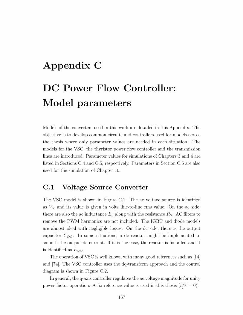
Appendix C
DC Power Flow Controller:
Model parameters
Models of the converters used in this work are detailed in this Appendix. The
objective is to develop common circuits and controllers used for models across
the thesis where only parameter values are needed in each situation. The
models for the VSC, the thyristor power flow controller and the transmission
lines are introduced. Parameter values for simulations of Chapters 3 and 4 are
listed in Sections C.4 and C.5, respectively. Parameters in Section C.5 are also
used for the simulation of Chapter 10.
C.1 Voltage Source Converter
The VSC model is shown in Figure C.1. The ac voltage source is identified
as Vac and its value is given in volts line-to-line rms value. On the ac side,
there are also the ac inductance LS along with the resistance RS. AC filters to
remove the PWM harmonics are not included. The IGBT and diode models
are almost ideal with negligible losses. On the dc side, there is the output
capacitor CDC . In some situations, a dc reactor might be implemented to
smooth the output dc current. If it is the case, the reactor is installed and it
is identified as Lreac.
The operation of VSC is well known with many good references such as [14]
and [74]. The VSC controller uses the dq-transform approach and the control
diagram is shown in Figure C.2.
In general, the q-axis controller regulates the ac voltage magnitude for unity
power factor operation. A fix reference value is used in this thesis (irefq = 0).
167
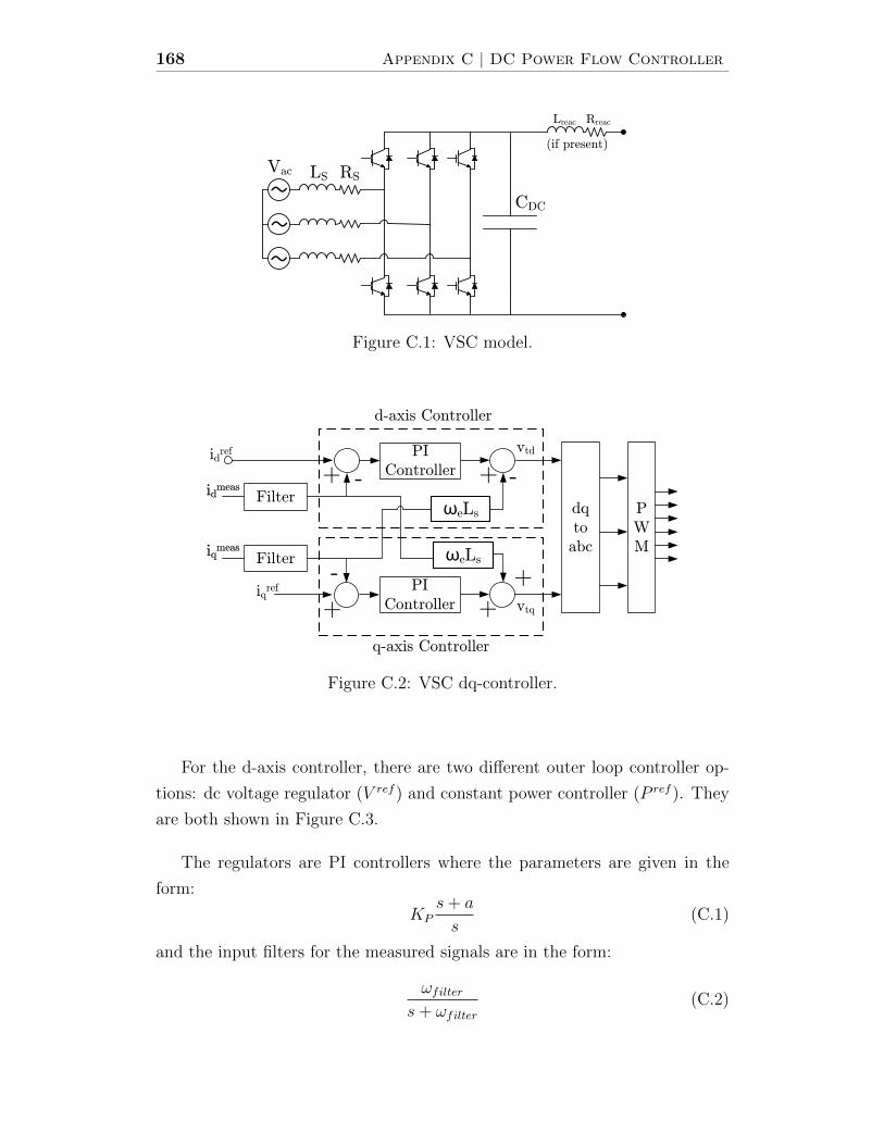
168 Appendix C | DC Power Flow Controller
~
~
~
LS RSVac
CDC
Lreac
(if present)
Rreac
Figure C.1: VSC model.
PI
Controller+ -idref
idmeas
eLs
+ -
iqmeas
+
-iqref
PI
Controller +
eLs
+
dq
to
abc
P
W
M
vtq
vtd
d-axis Controller
q-axis Controller
Filter
Filter
Figure C.2: VSC dq-controller.
For the d-axis controller, there are two different outer loop controller op-
tions: dc voltage regulator (V ref ) and constant power controller (P ref ). They
are both shown in Figure C.3.
The regulators are PI controllers where the parameters are given in the
form:
KPs+ a
s(C.1)
and the input filters for the measured signals are in the form:
ωfilters+ ωfilter
(C.2)

Model parameters | 169
idrefPI
Controller+ -
Vref
DC Voltage Controller
VmeasFilter
(a) DC voltage controller (V ref ).
idref
Imeas
PI
Controller+ -
Pref
Pmeas
Power Controller
Vmeas
Filter
Filter
(b) Power controller (P ref ).
Figure C.3: VSC d-axis controller options.
Transformer
Ldir
Linv
LDCV1:V2
LS RSVac
CDC
~~~
PCC
Figure C.4: VSC and thyristor power flow controller configuration.
C.2 Thyristor Power Flow Controller
The thyristor power flow controller connected to a VSC-HVDC station is shown
in Figure C.4. It is connected at the point of common coupling (PCC) of the
VSC via an ac transformer. The transformer has a power rating of Stransfo
in MVA and the voltage ratio V1 : V2 should be given. The leakage reactance
of the transformer model is set to 0.18pu. The connection of the transformer
is Y-Y where only the primary side is grounded. Each thyristor bridge has
its own dc reactor labelled: Ldir and Linv. In addition, a main dc reactor is
connected at the output of the dual configuration and it is identified as LDC .
The control schematic is illustrated in Figure C.5. The PI controllers are
given in the form:
KPs+ a
s(C.3)
and the input filters for the measured signals are in the form:
ωfilters+ ωfilter
(C.4)
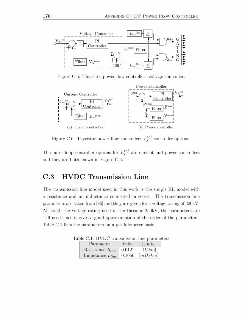
170 Appendix C | DC Power Flow Controller
PI
Controller+ -
VXmeas+
-
180°
dir
inv
VXref
Voltage Controller
Idcmeas
-iduallim
iduallim
Filter
Filter
GATING
-1
Figure C.5: Thyristor power flow controller: voltage controller.
PI
Controller+ -
Ilineref
Ilinemeas
VXref
Current Controller
Filter
(a) current controller.
VXref
Imeas
PI
Controller+ -
Pref
Pmeas
Power Controller
Vmeas
Filter
Filter
(b) Power controller.
Figure C.6: Thyristor power flow controller: V refX controller options.
The outer loop controller options for V refX are current and power controllers
and they are both shown in Figure C.6.
C.3 HVDC Transmission Line
The transmission line model used in this work is the simple RL model with
a resistance and an inductance connected in series. The transmission line
parameters are taken from [86] and they are given for a voltage rating of 320kV.
Although the voltage rating used in the thesis is 250kV, the parameters are
still used since it gives a good approximation of the order of the parameters.
Table C.1 lists the parameters on a per kilometer basis.
Table C.1: HVDC transmission line parametersParameter Value [Units]
Resistance Rline 0.0121 [Ω/km]Inductance Lline 0.1056 [mH/km]

Model parameters | 171
C.4 3-Terminal DC Grid (Chapter 3)
This section details in Table C.2 all the parameters for the simulations of
Chapter 3 done in PSCAD-EMTDC software package.
Table C.2: Simulation parameters of Chapter 3.VSC Parameters
T1 T2 T3Vac [kV RMS
LL ] 83 83 70fac [Hz] 50 50 50Ls / Rs [mH/Ω] 48.88/0.92 48.88/0.92 48.88/0.92CDC [mF] 0.2 0.2 0.4fswitching [kHz] 1.5 1.5 1.5
d-axis / q-axis controllersPI Controller: KP / a 10.8 / 18.8 10.8 / 18.8 10.8 / 18.8ωfilter [rad/s] 400 400 400Reference irefq 0.0 0.0 0.0
d-axis outer-loop controllerType P ref P ref V ref
Reference 160MW 80MW 250kVPI Controller: KP 10−4 10−4 0.025PI Controller: a 3.3× 10³ 3.3× 10³ 20ωfilter [rad/s] 150 150 150
Thyristor Power Flow Controller ParametersLDC [mH] 150Ldir, Linv [mH] 50Transformer [V1 : V2] 83:4.5Stransfo [MVA] 2.7
voltage controllerPI Controller: KP / a 10 / 15ωfilter [rad/s] 63ilimdual [kA] 0.05
current controllerPI Controller: KP / a 2.1 / 55ωfilter [rad/s] 63
Transmission Line ParametersLine L13 Line L23 Line L12
Distance [km] 248 83 165Resistance [Ω] 3 1 2Inductance [mH] 26.2 8.8 17.4Lreac [mH] 20 20 20
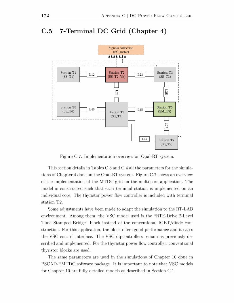
172 Appendix C | DC Power Flow Controller
C.5 7-Terminal DC Grid (Chapter 4)
L12
L46
L24
L23
L45
L5
7
L47
Station T1(SS_T1)
Station T2(SS_T2_Vx)
Station T4(SS_T4)
Station T6(SS_T6)
Station T7(SS_T7)
L3
5
Station T3(SS_T3)
Station T5(SM_T5)
Signals collection(SC_meter)
Figure C.7: Implementation overview on Opal-RT system.
This section details in Tables C.3 and C.4 all the parameters for the simula-
tions of Chapter 4 done on the Opal-RT system. Figure C.7 shows an overview
of the implementation of the MTDC grid on the multi-core application. The
model is constructed such that each terminal station is implemented on an
individual core. The thyristor power flow controller is included with terminal
station T2.
Some adjustments have been made to adapt the simulation to the RT-LAB
environment. Among them, the VSC model used is the “RTE-Drive 2-Level
Time Stamped Bridge” block instead of the conventional IGBT/diode con-
struction. For this application, the block offers good performance and it eases
the VSC control interface. The VSC dq-controllers remain as previously de-
scribed and implemented. For the thyristor power flow controller, conventional
thyristor blocks are used.
The same parameters are used in the simulations of Chapter 10 done in
PSCAD-EMTDC software package. It is important to note that VSC models
for Chapter 10 are fully detailed models as described in Section C.1.
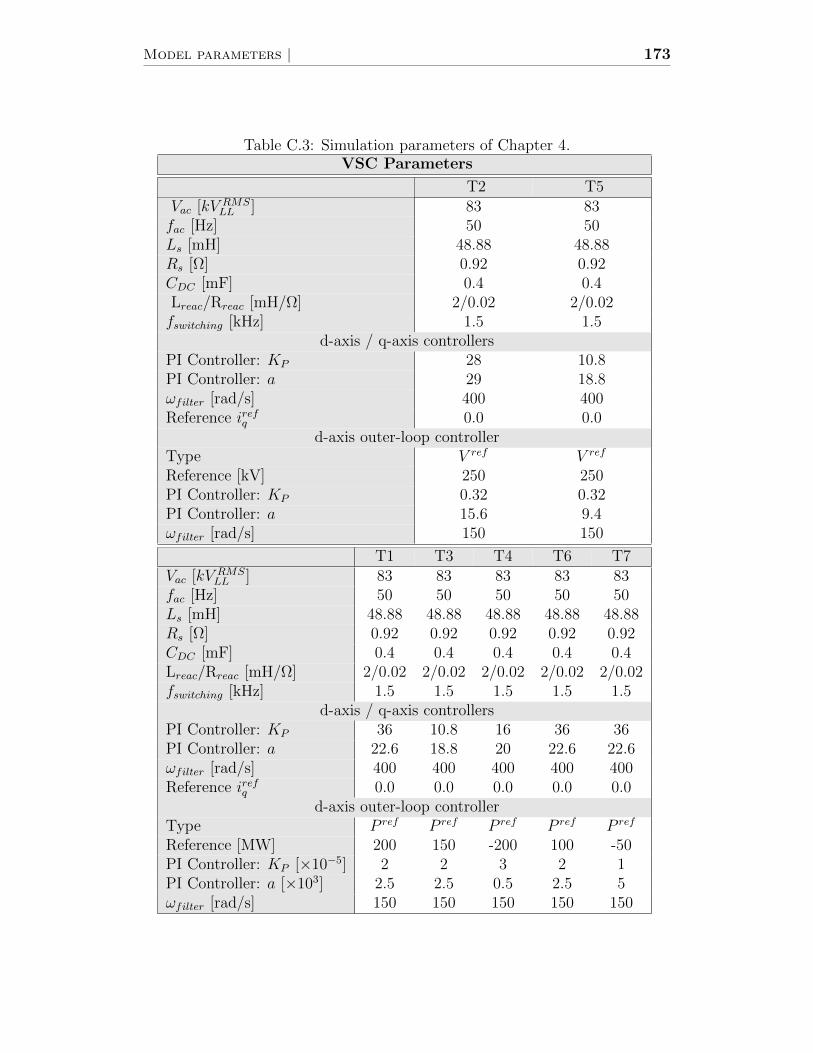
Model parameters | 173
Table C.3: Simulation parameters of Chapter 4.VSC Parameters
T2 T5Vac [kV RMS
LL ] 83 83fac [Hz] 50 50Ls [mH] 48.88 48.88Rs [Ω] 0.92 0.92CDC [mF] 0.4 0.4Lreac/Rreac [mH/Ω] 2/0.02 2/0.02fswitching [kHz] 1.5 1.5
d-axis / q-axis controllersPI Controller: KP 28 10.8PI Controller: a 29 18.8ωfilter [rad/s] 400 400Reference irefq 0.0 0.0
d-axis outer-loop controllerType V ref V ref
Reference [kV] 250 250PI Controller: KP 0.32 0.32PI Controller: a 15.6 9.4ωfilter [rad/s] 150 150
T1 T3 T4 T6 T7Vac [kV RMS
LL ] 83 83 83 83 83fac [Hz] 50 50 50 50 50Ls [mH] 48.88 48.88 48.88 48.88 48.88Rs [Ω] 0.92 0.92 0.92 0.92 0.92CDC [mF] 0.4 0.4 0.4 0.4 0.4Lreac/Rreac [mH/Ω] 2/0.02 2/0.02 2/0.02 2/0.02 2/0.02fswitching [kHz] 1.5 1.5 1.5 1.5 1.5
d-axis / q-axis controllersPI Controller: KP 36 10.8 16 36 36PI Controller: a 22.6 18.8 20 22.6 22.6ωfilter [rad/s] 400 400 400 400 400Reference irefq 0.0 0.0 0.0 0.0 0.0
d-axis outer-loop controllerType P ref P ref P ref P ref P ref
Reference [MW] 200 150 -200 100 -50PI Controller: KP [×10−5] 2 2 3 2 1PI Controller: a [×103] 2.5 2.5 0.5 2.5 5ωfilter [rad/s] 150 150 150 150 150
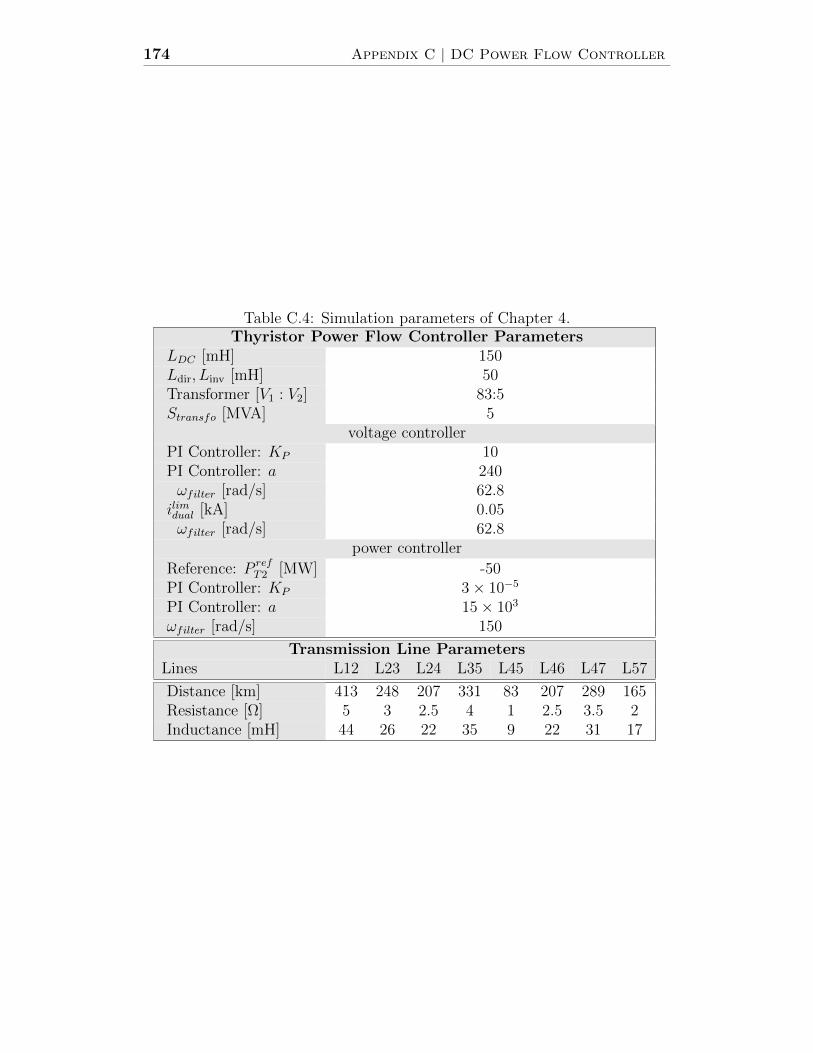
174 Appendix C | DC Power Flow Controller
Table C.4: Simulation parameters of Chapter 4.Thyristor Power Flow Controller Parameters
LDC [mH] 150Ldir, Linv [mH] 50Transformer [V1 : V2] 83:5Stransfo [MVA] 5
voltage controllerPI Controller: KP 10PI Controller: a 240ωfilter [rad/s] 62.8
ilimdual [kA] 0.05ωfilter [rad/s] 62.8
power controller
Reference: P refT2 [MW] -50
PI Controller: KP 3× 10⁻⁵
PI Controller: a 15× 103
ωfilter [rad/s] 150
Transmission Line ParametersLines L12 L23 L24 L35 L45 L46 L47 L57
Distance [km] 413 248 207 331 83 207 289 165Resistance [Ω] 5 3 2.5 4 1 2.5 3.5 2Inductance [mH] 44 26 22 35 9 22 31 17

Appendix D
Marx DC-DC Converter:
Prototype Details
D.1 Nameplate and Drawings
ETIENNE VEILLEUX
TITLE
Marx Converter Experiment
DATE Winter 2012
1-Stage Configuration
Rated Input Power 5kW
Rated Input Voltage 120Vdc
Rated Output Voltage 240Vdc
Converter Gain 2
Switching frequency 1949Hz
2-Stage Configuration
Rated Input Power 5kW
Rated Input Voltage 120Vdc
Rated Output Voltage 480Vdc
Converter Gain 4
L1:8uH Lout:75uH
Cout
SIND1
D1A
S1A
D2
C1BS1AA
C1A
f1 f2
360uF
360uF 230uF
f2
L2:50uH
D2A
S2A
Dout
C2BS2AA
C2A160uF
160uF
+
-
+15VGND
GATING
SWITCH
+
-
Figure D.1: Prototype nameplate.
175
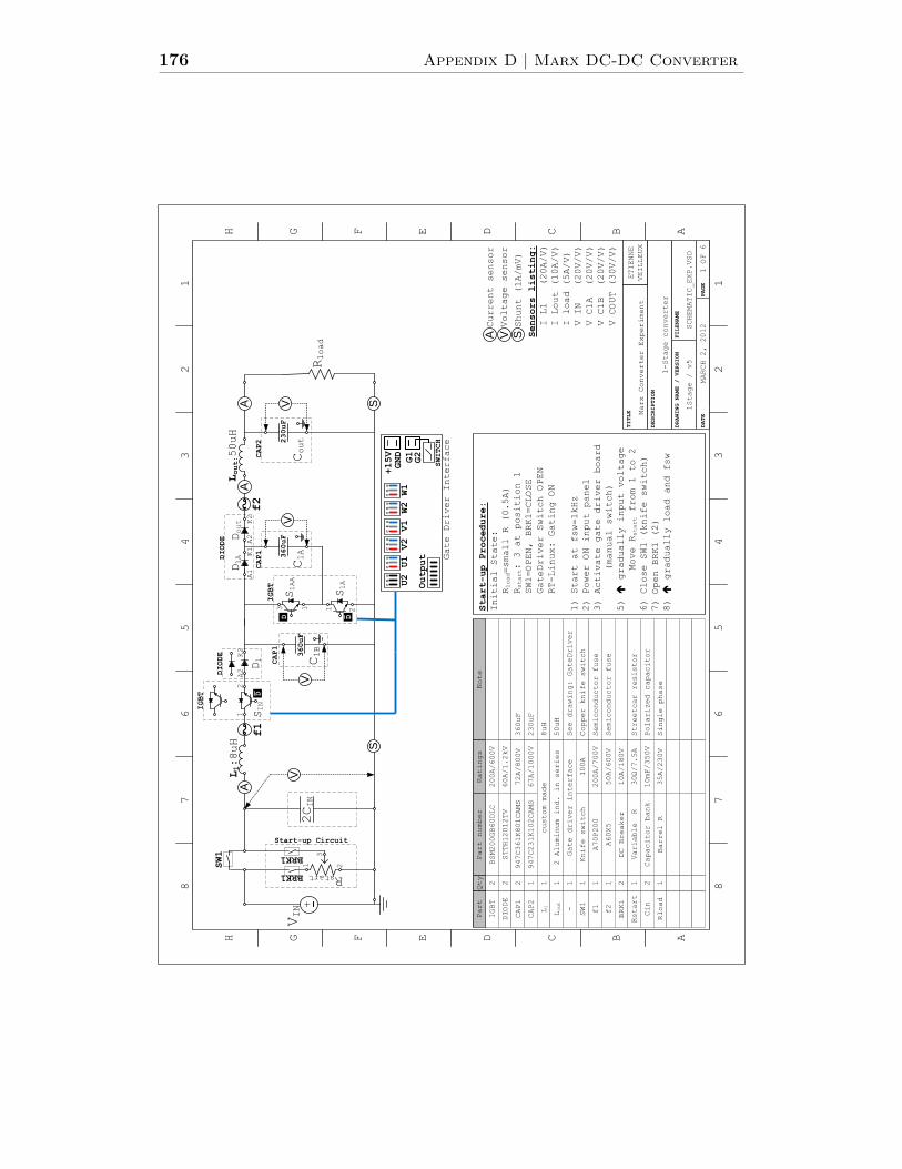
H G F E D C B A
87
65
43
21
H G F E D C B A
87
65
43
21
L1:8uH
Lout:50uH
Cout
Rload
SIN
D1
D1A
S1A
Dout
C1B
+
VIN
S1AAC1A
IGBT
DIODE
CAP1
DIODE
IGBT
12
A2
K2
A1
K1A2
K2
3 1 1 2
ETIENNE
VEILLEUX
DESCRIPTION
1-Stage converter
FILENAME
SCHEMATIC_EXP.VSD
TITLE Marx Converter Experiment
DRAWING NAME / VERSION
1Stage / v5
Part
Part number
Ratings
Note
IGBT
BSM200GB60DLC
200A/600V
DIODE
STTH12012TV
60A/1.2kV
CAP1
947C361K801CAMS
72A/800V
360uF
CAP2
947C231K102CAMS
67A/1000V
230uF
L1
custom made
8uH
Lout
2 Aluminum ind. in series
50uH
-Gate driver interface
See drawing: GateDriver
SW1
Knife switch
100A
Copper knife switch
f1
A70P200
200A/700V
Semiconductor fuse
f2
A60X5
50A/600V
Semiconductor fuse
BRK1
DC Breaker
10A/180V
Rstart
Variable R
30Ω/7.5A
Streetcar resistor
Cin
Capacitor bank
10mF/350V
Polarized capacitor
Rload
Barrel R
35A/230V
Single phase
Qty
2 2 2 1 1 1 1 1 1 1 2 1 2 1
CAP2
DATE
MARCH 2, 2012
PAGE
1 OF 6
f1
SW1
f2
BRK1
BRK1 Rstart
Start-up Circuit
Start-up Procedure:
Initial State:
Rload=small R (0.5A)
Rstart: 3 at position 1
SW1=OPEN, BRK1=CLOSE
GateDriver Switch OPEN
RT-Linux: Gating ON
1) Start at fsw=1kHz
2) Power ON input panel
3) Activate gate driver board
(manual switch)
5) é gradually input voltage
Move Rstart from 1 to 2
6) Close SW1 (knife switch)
7) Open BRK1 (2)
8) é gradually load and fsw
21
3
U2
U1
V2
V1
W2
W1
+15V
GND
G1
G2
Output Gate Driver Interface
C E G
C E G
C E G
C E G
C E G
C E G
SWITCH
2CIN
A
VV
V360uF
360uF
CAP1
230uF
AA V
SS
Sensors listing:
I L1
(20A/V)
I Lout (10A/V)
I load (5A/V)
V IN (20V/V)
V C1A (20V/V)
V C1B (20V/V)
V COUT (30V/V)
A V S
Current sensor
Voltage sensor
Shunt (1A/mV)
D
DD
176 Appendix D | Marx DC-DC Converter
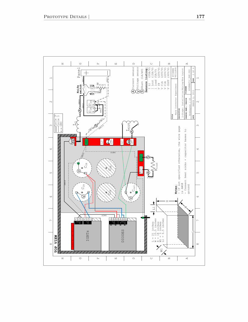
H G F E D C B A
87
65
43
21
H G F E D C B A
87
65
43
21
DATE
MARCH 2, 2012
DESCRIPTION
1-Stage: Installation/Wiring/Box Layout
FILENAME
SCHEMATIC_EXP.VSD
DRAWING NAME / VERSION
BoxLayout / v5
ETIENNE
VEILLEUX
TITLE Marx Converter Experiment
DIODES
IGBTs
Gate Driver Board
TOP VIEW
Cout
C2A
C2BC1B
C1A
SIN S1 D1 D1A+
PAGE
2 OF 6
L1
GND
L2+
L2-
LO+
LO-
OUT+
OUT-
+
-- + + -
LOUT
L = 21 inches
W = 15.5 inches
H = 18 inches
Notes:
- If not specified otherwise, the wire gage
is AWG8
- Connect heat sinks + capacitor bases to
ground
L
H
W
W1
L1
W1 = 3 inches
L1 = 6.5 inches
123 123K2
AWG4
AWG4
AWG4
AWG4
Panel
Rload
A2K1A1
K2A2K1A1
10A
10ARstart
12
3
Knife
switch
AWG10
AWG10
V
V
V
AWG10
AS
A
AWG2
AAWG4
Sensors listing:
I L1
(20A/V)
I Lout (10A/V)
I load (5A/V)
V IN (20V/V)
V C1A (20V/V)
V C1B (20V/V)
V COUT (30V/V)
A V S
Current sensor
Voltage sensor
Shunt (1A/mV)
200A
50A
AWG2AWG2
AWG2
+-
CIN
+-
CIN
S
AWG2
AWG2
Cycle D’
Cycle D
GND
Prototype Details | 177

H G F E D C B A
87
65
43
21
H G F E D C B A
87
65
43
21
L1:8uH
Lout:75uH
Cout
Rload
SIN
D1
D1A
S1A
D2
C1B
+
VIN
S1AA
C1A
IGBT
DIODE
CAP1
DIODE
IGBT
12A2
K2
A1
K1A2
K2
3 1 1 2
ETIENNE
VEILLEUX
DESCRIPTION
2-Stage converter
FILENAME
SCHEMATIC_EXP.VSD
TITLE Marx Converter Experiment
DRAWING NAME / VERSION
2Stage / v1
Part
Part number
Ratings
Note
IGBT
BSM200GB60DLC
200A/600V
DIODE
STTH12012TV
60A/1.2kV
CAP1
947C361K801CAMS
72A/800V
360uF
CAP2
947C231K102CAMS
67A/1000V
230uF
L1
custom made
8uH
L2
2 Aluminum ind. in series
50uH
-Gate driver interface
See drawing: GateDriver
SW1
Knife switch
100A
Copper knife switch
f1
A70P200
200A/700V
Semiconductor fuse
f2
A60X5
50A/600V
Semiconductor fuse
BRK1
DC Breaker
10A/180V
Rstart
Variable R
30Ω/7.5A
Streetcar resistor
Cin
Capacitor bank
10mF/350V
Polarized capacitor
Rload
Barrel R
35A/230V
Single phase
CAP3
947C161K122CAMS
62A/1200V
160uF
Lout
75uH
Qty
3 3 2 1 1 1 1 1 1 2 2 12 12 1
CAP2
DATE
MARCH 12, 2012
PAGE
3 OF 6
f1
SW1
f2
BRK1
BRK1 Rstart
Start-up Circuit
21
3
U2
U1
V2
V1
W2
W1
+15V
GND
G1
G2
Output Gate Driver Interface
C E G
C E G
C E G
C E G
C E G
C E G
SWITCH
2CINA
VV
360uF
360uF
CAP1
230uF
AA V
SS
f2
L2:50uH
AD2A
S2A
Dout
C2B
S2AA
C2A
CAP3
DIODE
IGBT
A1
K1A2
K2
3 1 1 2
V160uF
160uF
CAP3
D
D
D
D D
A V S
Current sensor
Voltage sensor
Shunt (1A/mV)
Sensors listing:
I L1
(20A/V)
I L2 (10A/V)
I Lout (20A/V)
I load (5A/V)
V IN (20V/V)
V C1B (30V/V)
V C2B (30V/V)
V COUT (70V/V)
178 Appendix D | Marx DC-DC Converter
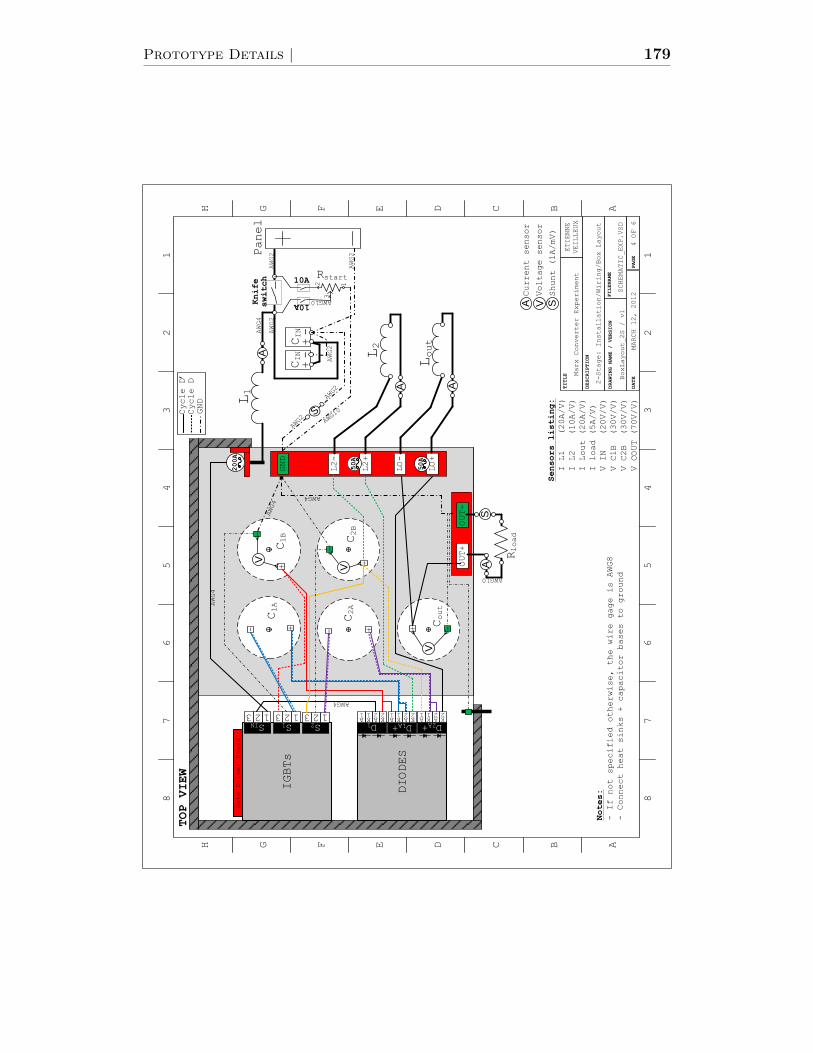
H G F E D C B A
87
65
43
21
H G F E D C B A
87
65
43
21
DATE
MARCH 12, 2012
DESCRIPTION
2-Stage: Installation/Wiring/Box Layout
FILENAME
SCHEMATIC_EXP.VSD
DRAWING NAME / VERSION
BoxLayout_2S / v1
ETIENNE
VEILLEUX
TITLE Marx Converter Experiment
DIODES
IGBTs
Gate Driver Board
TOP VIEW
Cout
C2A
C2B
C1B
C1A
SIN S1 D1 D1A+
PAGE
4 OF 6
L1
GND
L2+
L2-
LO+
LO-
OUT+
OUT-
+
-- + + -
L2
Notes:
- If not specified otherwise, the wire gage is AWG8
- Connect heat sinks + capacitor bases to ground
123 123K2
AWG4
AWG4
AWG4
AWG4
Panel
Rload
A2K1A1
K2A2K1A1
10A
10ARstart
12
3
Knife
switch
AWG10
AWG10
V
V
AWG10
AS
A
AWG2
AAWG4
200A
AWG2
AWG2
AWG2
+-
CIN
+-
CIN
S
AWG2
Lout
A
50A
50A
Cycle D’
Cycle D
GND
- +
-
+
S2123
D2A+K2A2K1A1
V
A V S
Current sensor
Voltage sensor
Shunt (1A/mV)
Sensors listing:
I L1
(20A/V)
I L2 (10A/V)
I Lout (20A/V)
I load (5A/V)
V IN (20V/V)
V C1B (30V/V)
V C2B (30V/V)
V COUT (70V/V)
AWG2
Prototype Details | 179

H G F E D C B A
87
65
43
21
H G F E D C B A
87
65
43
21
D:S1A
D:S2AA
Notes:
- G1 PWM : switching
- G2 signal BLOCK: LOW=BLOCK, HIGH=ON
- Output signals: +VDC=no error, GND = error
01
02
03
04
05
06
07
08
09
10
11
12
13
14
15
16
17
18
19
20
21
22
23
24
25
26
27
28
29
30
31
32
33
34
68
67
66
65
64
63
62
61
60
59
58
57
56
55
54
53
52
51
50
49
48
47
46
45
44
43
42
41
40
39
38
37
36
35
GNDU_S02U_MODU_RC2U_INBU_INAU_RC1U_VLU_SO1GNDGNDVDCVDC
GNDGNDVDDVDD
GND
U_C2U_RTH2U_E2U_G2
V_S02V_MODV_RC2V_INBV_INAV_RC1V_VLV_SO1
W_S02W_MODW_RC2W_INBW_INAW_RC1W_VLW_SO1
U_C1U_RTH1U_E1U_G1
V_C2V_RTH2V_E2V_G2
V_C1V_RTH1V_E1V_G1
W_C2W_RTH2W_E2W_G2
W_C1W_RTH1W_E1W_G1
CT-CONCEPT 6SD10EI
+15V
GND
33
kΩ
1kΩ
220
pF
1kΩ
1kΩ
33
kΩ
220
pF
33
kΩ
220
pF
33
kΩ
220
pF
33
kΩ
220
pF
33
kΩ
220
pF
U2
U1
V2
V1
W2
W1
Deatime
UV
W
Logic Level
U2:-
Output Signal
400mA
Feb.1: Connections verified
Feb.7: Gating signals verified
Mar. 18: Complete gating recorded
G1:PWMG2:BLOCK
20kΩ
1N4007
5Ω
W1
C E G
U2
C E G
20kΩ
1N4007
5Ω
U1
C E G
20kΩ
1N4007
5Ω
V2
C E G
20kΩ
1N4007
5Ω
V1
C E G
D:SIN
6
7
1
Zener15V
4
5
3
Zener15V
6
7
1
Zener15V
6
7
1
Zener15V
4
5
3
Zener15V
D:S1AA
D:S2A Twisted wires
SWITCH
1:brown
1a:GND
1b:Vdc
DATE
MARCH 18, 2012
DESCRIPTION
Gate driver interface
FILENAME
SCHEMATIC_EXP.VSD
DRAWING NAME / VERSION
GateDriver / v6
ETIENNE
VEILLEUX
TITLE Marx Converter Experiment
GND
U1:blue
V2:black
V1:white
W2:red
W1:yellow
red
white
20kΩ
1N4007
5Ω
W2
C E G
blue
PAGE
5 OF 6
DB9
180 Appendix D | Marx DC-DC Converter

H G F E D C B A
87
65
43
21
H G F E D C B A
87
65
43
21
DATE
MARCH 19, 2012
DESCRIPTION
Installation notes and various
FILENAME
SCHEMATIC_EXP.VSD
DRAWING NAME / VERSION
Various
ETIENNE
VEILLEUX
TITLE Marx Converter Experiment
Diode / IGBT
connections
PAGE
6 OF 6
Copper Wire - Maximum Current in Ampere
Temperature rating of wire
AWG | 60°C / 75°C / 90°C |
2 | 140 / 170 / 190 |
4 | 105 / 125 / 140 |
6 | 80 / 95 / 105 |
8 | 60 / 70 / 80 |
10 | 40 / 50 / 55 |
Reference: NEC Standards Table 310.171 23
Pre Start-up Check List
Start-Up Procedures
[1] Start at fsw 1kHz
[2] Power ON input panel
[3] Activate gate driver board
(manual switch)
[4] Increase gradually input voltage
Move Rstart from 1 to 2
Capacitor voltage increases
[5] Close SW1 (knife switch)
[6] Open BRK1 (2)
Start-up resistor completely
disconnected
[7] Increase gradually: load and fsw 2kHZ
Shut Down Procedures
Turn ON
barrel resistor fan
heat sinks fans
dc power supply gate driver board
dc power supply voltage sensors
current sensors
OPEN switch gate driver board
Small R barrel resistor ( 0.5A )
OPEN knife switch SW1
CLOSE breaker BRK1
CLOSE breaker BRK1
Variable resistor position 1 (GND)
Start gating from RT-LINUX
[1] Reduce load (2.5A)
[2] Power OFF input panel
[3] Deactivate gate driver board
(manual switch)
[4] Close BRK1 (2)
[5] Open SW1 (knife switch)
Make sure all capacitors are discharged
Lout:75uH Cout
Rload
CAP2 230uF
Af2
L2:50uH
D2A
S2A
Dout
C2B
S2AA
C2A
CAP3
DIODE
IGBT
A1
K1A2
K2
3 1 1 2
160uF
160uF
CAP3
D D
Go from 2-stage to 1-stage configuration
Cable ratings table
1) Remove wire [VC2B- to GND]
2) Remove wire [VC2B+ to L2-]
3) Change wire [Cout+ to Lout-] to [Cout+ to L2-]
4) L2- remains unconnected
*No need to touch gate drivers
Prototype Details | 181

182 Appendix D | Marx DC-DC Converter
D.2 Pictures
Figure D.2: Gate driver interface board.
(a) L1: custom-made air-core inductormade with Litz wire.
(b) LOUT : custom-madeferrite-core inductor madewith Litz wire.
(c) L2: air-core inductor made with aluminum.
Figure D.3: Inductors used for experimental work.
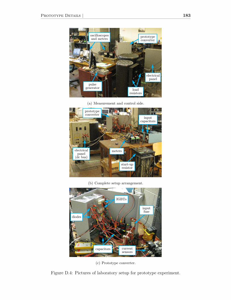
Prototype Details | 183
loadresistors
electricalpanel
pulsegenerator
prototypeconverter
oscilloscopesand meters
(a) Measurement and control side.
electricalpanel(dc bus)
meters
prototypeconverter
start-upresistor
inputcapacitors
(b) Complete setup arrangement.
capacitors
inputfuse
IGBTs
diodes
currentsensors
(c) Prototype converter.
Figure D.4: Pictures of laboratory setup for prototype experiment.
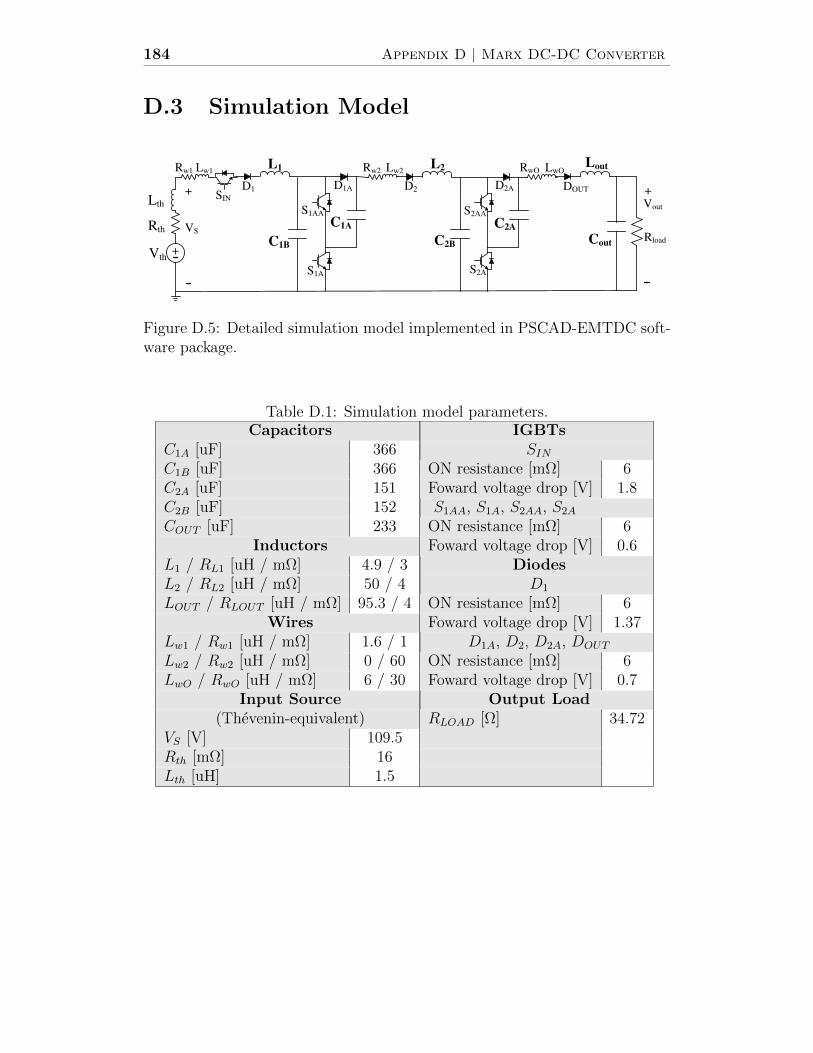
184 Appendix D | Marx DC-DC Converter
D.3 Simulation Model
+
L1Lout
CoutRload
Vth
SIN
D1
S1AA
Vout
C1B
C1A
D2
C2B
C2A
S1AS2A
S2AA
DOUTD1A D2A
L2
Lth
Rth
+
VS
Rw1 Lw1 Rw2 Lw2 RwO LwO
+
Figure D.5: Detailed simulation model implemented in PSCAD-EMTDC soft-ware package.
Table D.1: Simulation model parameters.Capacitors IGBTs
C1A [uF] 366 SINC1B [uF] 366 ON resistance [mΩ] 6C2A [uF] 151 Foward voltage drop [V] 1.8C2B [uF] 152 S1AA, S1A, S2AA, S2A
COUT [uF] 233 ON resistance [mΩ] 6Inductors Foward voltage drop [V] 0.6
L1 / RL1 [uH / mΩ] 4.9 / 3 DiodesL2 / RL2 [uH / mΩ] 50 / 4 D1
LOUT / RLOUT [uH / mΩ] 95.3 / 4 ON resistance [mΩ] 6Wires Foward voltage drop [V] 1.37
Lw1 / Rw1 [uH / mΩ] 1.6 / 1 D1A, D2, D2A, DOUT
Lw2 / Rw2 [uH / mΩ] 0 / 60 ON resistance [mΩ] 6LwO / RwO [uH / mΩ] 6 / 30 Foward voltage drop [V] 0.7
Input Source Output Load(Thevenin-equivalent) RLOAD [Ω] 34.72
VS [V] 109.5Rth [mΩ] 16Lth [uH] 1.5
Bibliography
[1] Siemens, “Siemens to deliver new HVDC technolgy for low-loss power
supply via submarine cable to San Francisco,” [Press release], Available:
www.energy.siemens.com.
[2] S. P. Teeuwsen, “Modeling the Trans Bay Cable Project as Voltage-
Sourced Converter with Modular Multilevel Converter Design,” in IEEE
Power and Energy Society General Meeting, July 2011.
[3] ABB, “Grid connection of offshore wind farms - BorWin1,” [Brochure],
Available: www.abb.com/hvdc.
[4] U. Lamm, E. Uhlmann, and P. Danfors, “Some Aspects of Tapping
H.V.D.C. Transmission Systems,” Direct Current, vol. 8, no. 5, pp. 124–
129, May 1963.
[5] R. Foerst, G. Heyner, K. Kanngiesser, and H. Waldmann, “Multitermi-
nal operation of hvdc converter stations,” IEEE Transactions on Power
Apparatus and Systems, vol. PAS-88, pp. 1042–1052, 1969.
[6] G. Asplund, B. Jacobson, B. Berggren, and K. Linden, “Continental Over-
lay HVDC-Grid ,” in CIGRE 2010 Session, 2010.
[7] S. Gordon, “Supergrid to the rescue,” PowerEngineer, vol. 20, no. 5, pp.
30–33, 2006.
[8] P. Fairley, “A Supergrid for Europe,” Technology Review, March 2006.
[9] D. Van Hertem and M. Ghandhari, “Multi-terminal VSC HVDC for the
European supergrid: Obstacles,” Renewable and Sustainable Energy Re-
views, vol. 14, no. 9, pp. 3156–3163, 2010.
[10] G. Asplund, “HVDC grids - possibilities and challenges,” in CIGRE SC
B4 2009 Bergen Colloquium, 2009.
185
186 BIBLIOGRAPHY
[11] BARD Engineering GmbH, “Electricity from the SEA,” BARD Magazine,
no. 12, pp. 4–7, July 2010. [Online]. Available: www.bard-offshore.de
[12] Tennet TSO B.V., “ BorWin1 The world’s longest direct current connec-
tion ,” [Brochure], Available: www.tennettso.de.
[13] CIGRE Working Group B3.26, “Guidelines for the Design and Construc-
tion of AC Offshore Substations for Wind Power Plants,” Brochure 483,
Dec. 2011.
[14] J. Arrillaga, Y. H. Liu, and N. R. Watson, Flexible Power Transmission:
The HVDC Options. John Wiley & Sons, 2007.
[15] N. G. Hingorani and L. Gyugyi, Understanding FACTS: Concepts and
Technology of Flexible AC Transmission Systems. John Wiley & Sons,
2000.
[16] A. Lesnicar and R. Marquardt, “An innovative modular multilevel con-
verter topology suitable for a wide power range,” in IEEE Bologna Pow-
erTech Conference, vol. 3, 2003.
[17] S. Allebrod, R. Hamerski, and R. Marquardt, “New Transformerless, Scal-
able Modular Multilevel Converters for HVDC-transmission,” in IEEE
Power Electronics Specialists Conference, June 2008, pp. 174–179.
[18] L. Tang and B. T. Ooi, “ Protection of VSC-multi-terminal HVDC against
DC faults,” in IEEE 33rd Annual Power Electronics Specialists Confer-
ence, vol. 2, June 2002, pp. 719–724.
[19] C. Meyer, M. Kowal, and R. W. De Doncker, “Circuit breaker concepts for
future high-power DC-applications,” in 14th Industry Applications Society
Annual Meeting, vol. 2, Oct. 2005, pp. 860–866.
[20] J. Yang, J. E. Fletcher, and J. O’Reilly, “Multiterminal DC Wind Farm
Collection Grid Internal Fault Analysis and Protection Design,” IEEE
Trans. on Power Del., vol. 25, pp. 2308–2318, Oct. 2010.
[21] J. Hafner and B. Jacobson, “Proactive Hybrid HVDC Breakers - A key
innovation for reliable HVDC grids,” in CIGRE 2011 Bologna Symposium,
2011.
BIBLIOGRAPHY 187
[22] C. M. Franck, “HVDC Circuit Breakers: A Review Identifying Future
Research Needs,” IEEE Trans. on Power Del., vol. 26, pp. 998–1007,
April 2011.
[23] J. Descloux, P. Rault, S. Nguefeu, J. Curis, X. Guillayd, F. Colas, and
B. Raison, “HVDC meshed grid: Control and protection of a multi-
terminal HVDC system,” in CIGRE 2012 Session, 2012.
[24] D. G. Chapman, J. B. Davies, J. R. McNichol, E. M. Gulachenski, S. Doe,
and N. J. Balu, “Test experience with multiterminal HVDC load flow and
stability programs,” IEEE Trans. Power Del., vol. 3, pp. 1173–1181, July
1988.
[25] C. D. Barker and R. Whitehouse, “Autonomous converter control in a
multi-terminal HVDC system,” in IET International Conference on AC
and DC Power Transmission, Oct. 2010.
[26] J. Liang, T. Jing, O. Gomis-Bellmunt, J. Ekanayake, and N. Jenkins, “Op-
eration and Control of Multiterminal HVDC Transmission for Offshore
Wind Farms,” IEEE Trans. Power Del., vol. 26, no. 4, pp. 2596–2604,
Oct. 2011.
[27] D. Jovcic and B. T. Ooi, “Developing DC Transmission Networks Using
DC Transformers,” IEEE Trans. Power Del., vol. 25, pp. 2535 –2543, Oct.
2010.
[28] E. Prieto-Araujo, F. D. Bianchi, A. Junyent-Ferre, and O. Gomis-
Bellmunt, “Methodology for Droop Control Dynamic Analysis of Mul-
titerminal VSC-HVDC Grids for Offshore Wind Farms,” IEEE Trans.
Power Del., vol. 26, pp. 2476–2485, Oct. 2011.
[29] C. Dierckxsens, K. Srivastava, M. Reza, S. Cole, J. Beerten, and R. Bel-
mans, “ A distributed DC voltage control method for VSC MTDC sys-
tems,” Electric Power Systems Research, vol. 82, no. 1, pp. 54–58, Jan.
2012.
[30] T. M. Haileselassie and K. Uhlen, “Precise control of power flow in multi-
terminal VSC-HVDCs using DC voltage droop control,” in IEEE Power
and Energy Society General Meeting, July 2012.

188 BIBLIOGRAPHY
[31] F. Schettler, G. Balzer, M. Hyttinen, S. E. Rye, and T. Westerweller,
“Technical guidelines for first HVDC grids - A European study group
based on an initiative of the German commission for electrical, electronic
& information technologies,” in CIGRE 2012 Session, 2012.
[32] P. Kundur, Power System Stability and Control. McGraw-Hill, 1994.
[33] M. Liserre, R. Cardenas, M. Molinas, and J. Rodriguez, “Overview of
Multi-MW Wind Turbines and Wind Parks,” IEEE Trans. Ind. Electron.,
vol. 58, pp. 1081–1095, April 2011.
[34] T. K. Vrana and O. B. Fosso, “Technical aspects of the North Sea Super
Grid,” Electra, no. 258, pp. 5–19, Oct. 2011.
[35] C. Meyer, M. Hoing, A. Peterson, and R. W. De Doncker, “Control and
Design of DC Grids for Offshore Wind Farms,” IEEE Trans. on Ind.
Appl., vol. 43, pp. 1475–1482, Nov./Dec. 2007.
[36] P. K. Steimer and O. Apeldoorn, “Medium voltage power conversion
technology for efficient windpark power collection grids,” in IEEE In-
ternational Symposium on Power Electronics for Distributed Generation
Systems, June 2010.
[37] J. Robinson, D. Jovcic, and G. Joos, “Analysis and Design of an Offshore
Wind Farm Using a MV DC Grid,” IEEE Trans. Power Del., vol. 25, pp.
2164 –2173, Oct. 2010.
[38] S. M. Muyeen, R. Takahashi, and J. Tamura, “Operation and Control of
HVDC-Connected Offshore Wind Farm,” IEEE Trans. Sustainable En-
ergy, vol. 1, pp. 30–37, April 2010.
[39] F. Deng and Z. Chen, “An Offshore Wind Farm with DC Grid Connection
and Its Performance under Power System Transients,” in IEEE Power and
Energy Society General Meeting, July 2011.
[40] R. W. Erickson and D. Maksimovic, Fundamentals of Power Electronics,
2nd ed. Springer, 2001.
[41] N. Mohan, T. M. Undeland, and W. P. Robbins, Power Electronics: Con-
verters, Applications and Design, 3rd ed. John Wiley & Sons, 2002.
BIBLIOGRAPHY 189
[42] D. W. Hart, Introduction to Power Electronics. Prentice Hall, 1997.
[43] F. L. Luo and H. Ye, Advanded DC/DC Converters. CRC Press LLC,
2004.
[44] E. Marx, Verfahren zur Schlagprufung von Isolatoren und anderen elek-
trischen Vorrichtungen. German Patent 455933, 1923.
[45] E. Marx, “Versuche uber die Prufung von Isolatoren mit Span-
nungsstoßen,” Elektrotechnische Zeitschrift, vol. 45, pp. 652–654, June
1924.
[46] ABB Power T&D Company Inc., Electrical Transmission and Distribution
Reference Book, 5th ed. ABB Power T&D Company Inc., 1997.
[47] C. G. Clayton, “The generation of recurring high-voltage X-ray impulses,”
Proceedings of the IEE - Part I: General, vol. 119, pp. 206–213, Sept. 1952.
[48] O. Abutbul, A. Gherlitz, Y. Berkovich, and A. Ioinovici, “Step-up
switching-mode converter with high voltage gain using a switched-
capacitor circuit,” IEEE Trans. Circuits Syst. I, Fundam. Theory Appl.,
vol. 50, pp. 1098–1102, Aug. 2003.
[49] J. W. Baek, D. W. Yoo, G. H. Rim, and J. Lai, “Solid State Marx Gener-
ator Using Series-Connected IGBTs,” IEEE Trans. Plasma Sci., vol. 33,
pp. 1198–1204, Aug. 2005.
[50] L. M. Redondo, J. F. Silva, P. Tavares, and E. Margato, “All Silicon Marx-
bank Topology for High-voltage, High-frequency Rectangular Pulses,” in
IEEE 36th Power Electronics Specialists Conference, June 2005, pp. 1170–
1174.
[51] M. D. Seeman and S. R. Sanders, “Analysis and Optimization of Switched
Capacitor DC-DC Converters,” IEEE Trans. Power Electon., vol. 23, pp.
841–851, March 2008.
[52] L. M. Redondo and J. F. Silva, “Repetitive High-Voltage Solid-State Marx
Modulator Design for Various Load Conditions,” IEEE Trans. Plasma
Sci., vol. 37, pp. 1632–1637, Aug. 2009.

190 BIBLIOGRAPHY
[53] S. Bae, A. Kwasinski, M. M. Flynn, and R. E. Hebner, “High-Power
Pulse Generator With Flexible Output Pattern ,” IEEE Trans. on Power
Electron., vol. 25, pp. 1675–1684, July 2010.
[54] L. M. Redondo, “A DC Voltage-Multiplier Circuit Working as High-
Voltage Pulse Generator,” IEEE Trans. Plasma Sci., vol. 38, pp. 2725–
2729, Oct. 2010.
[55] S. Zabihi, Z. Zabihi, and F. Zare, “A Solid-State Marx Generator With a
Novel Configuration,” IEEE Trans. Plasma Sci., vol. 39, pp. 1721–1728,
Aug. 2011.
[56] M. A. Kemp, A. Benwell, C. Burkhart, R. Larsen, D. MacNair,
M. Nguyen, and J. Olsen, “Status Update on the Second-Generation ILC
Marx Modulator Prototype,” in IEEE Int. Power Modulator and High
Voltage Conf., 2010, pp. 23–26.
[57] M. A. Kemp, A. Benwell, C. Burkhart, R. Larsen, D. MacNair,
M. Nguyen, and J. Olsen, “Final Design of the SLAC P2 Marx Klystron
Modulator,” in 2011 IEEE Pulsed Power Conf., 2011, pp. 1582–1589.
[58] J. J. Cooley and S. B. Leeb, “ Per panel photovoltaic energy extrac-
tion with multilevel output DC-DC switched capacitor converters,” in
26th Annu. IEEE Applied Power Electronics Conf. and Expo., 2011, pp.
pp.419–428.
[59] A. Lopez, R. Diez, G. Perilla, and D. Patino, “Analysis and Comparison
of Three Topologies of the Ladder Multilevel DC/DC Converter,” IEEE
Trans. on Power Electron., vol. 27, pp. 3119–3127, July 2012.
[60] S. B. Ok, H. J. Ryoo, S. R. Jang, S. H. Ahn, and G. Goussev, “De-
sign of a High-Efficiency 40-kV, 150-A, 3-kHz Solid-State Pulsed Power
Modulator,” IEEE Trans. on Plasma Sci., vol. 40, pp. 2569–2577, Oct.
2012.
[61] T. Sakamoto, A. Nami, M. Akiyama, and H. Akiyama, “A Repetitive
Solid State Marx-Type Pulsed Power Generator Using Multistage Switch-
Capacitor Cells,” IEEE Trans. on Plasma Sci., vol. 40, pp. 2316–2321,
Oct. 2012.
BIBLIOGRAPHY 191
[62] R. D. Middlebrook, “Transformerless DC-to-DC converters with large
conversion ratios,” IEEE Trans. Power Electron., vol. 3, pp. 484–488,
Oct. 1988.
[63] J. A. Morales-Saldana, E. E. C. Gutierrez, and J. Leyva-Ramos, “Model-
ing of switch-mode dc-dc cascade converters,” IEEE Trans. Aerosp. Elec-
tron. Syst., vol. 38, pp. 295–299, Jan. 2002.
[64] F. L. Luo and H. Ye, “Positive output cascade boost converters,” IEE
Proc. - Electric Power Applications, vol. 151, no. 5, pp. 590–606, Sept.
2004.
[65] M. G. Ortiz-Lopez, J. Leyva-Ramos, E. E. Carbajal-Gutierrez, and J. A.
Morales-Saldana, “Modelling and analysis of switch-mode cascade con-
verters with a single active switch,” IET Power Electronics, vol. 1, no. 4,
pp. 478–487, Dec. 2008.
[66] D. Jovcic and B. T. Ooi, “Tapping on HVDC lines using DC transform-
ers,” Electric Power Systems Research, vol. 81, no. 2, pp. 561–569, Feb.
2011.
[67] W. F. Long, J. Reeve, J. R. McNichol, M. S. Holland, J. P. Taisne,
J. LeMay, and D. J. Lorden, “Application aspects of multiterminal DC
power transmission,” IEEE Trans. Power Del., vol. 5, pp. 2084–2098, Oct.
1990.
[68] A. Ekstrom and P. Lamell, “HVDC tapping station: power tapping from a
DC transmission line to a local AC network,” in International Conference
on AC and DC Power Transmission, Sept. 1991, pp. 126–131.
[69] Z. Zhao and M. R. Iravani, “Application of GTO voltage-source inverter
for tapping HVDC power,” IEE Proc. - Generation, Transmission and
Distribution,, vol. 141, no. 1, pp. 19–26, Jan. 1994.
[70] M. R. Aghaebrahimi and R. W. Menzies, “Small power tapping from
HVDC transmission systems: a novel approach,” IEEE Trans. Power
Del., vol. 12, pp. 1698–1703, Oct. 1997.
[71] G. Asplund and A. Williamson, “A novel approach to providing on route
power supplies to rural and urban communities in close proximity to the

192 BIBLIOGRAPHY
extra high voltage DC transmission line,” in IEEE PES Conference and
Exposition in Africa, July 2007.
[72] P. C. Sen, Thyristors DC Drives. Wiley-Interscience, 1981.
[73] C.-K. Kim, V. K. Sood, G.-S. Jang, S.-J. Lim, and S.-J. Lee, HVDC
Transmission: Power Conversion Applications in Power Systems. Wiley-
IEEE Press, 2009.
[74] A. Yazdani and R. Iravani, Voltage-Sources Converters in Power Systems:
Modeling, Control and Applications. John Wiley & Sons, 2010.
[75] Opal-RT Technologies, “RT-LAB Version 10.2 User Guide,” 2007.
[76] G. F. Franklin, J. D. Powell, and A. Emami-Naeini, Feedback Control of
Dynamic Systems, 5th ed. Prentice Hall, 2009.
[77] R. E. Thomas and A. J. Rosa, The Analysis and Design of Linear Circuits:
Laplace Early, 4th ed. John Wiley & Sons, 2004.
[78] S. Lee, “Optimum design and selection of heat sinks,” IEEE Trans. Com-
pon. Packag. Manuf. Technol. A, vol. 18, pp. 812–817, Dec. 1995.
[79] D. S. Watkins, Fundamentals of Matrix Computations, 2nd ed. John
Wiley & Sons, 2002.
[80] I. N. Bronshtein, K. A. Semendyayev, G. Musiol, and H. Muehlig, Hand-
book of Mathematics, 5th ed. Springer, 2007.
[81] E. Veilleux and P. W. Lehn, “Interconnection of direct-drive wind turbines
using a distributed HVDC converter station,” in 35th Annual Conference
of IEEE Industrial Electronics, Nov. 2009.
[82] E. Veilleux, “Interconnection of Direct-Drive Wind Turbines Using a Se-
ries Connected DC Grid,” Master’s thesis, University of Toronto, 2009.
[83] Z. Chen and E. Spooner, “Grid Power Quality with Variable Speed Wind
Turbines,” IEEE Trans. Energy Convers., vol. 16, pp. 148–154, June 2001.
[84] CIGRE Working Group B4, “Study committee B4 Annual Report 2011,”
Electra, no. 262, pp. 17–21, June 2012.

BIBLIOGRAPHY 193
[85] J. D. Glover, M. S. Sarma, and T. J. Overbye, Power System Analysis
and Design, 4th ed. Thomson, 2008.
[86] D. Van Hertem, M. Ghandhari, J. B. Curis, O. Despouys, and A. Marzin,
“Protection requirements for a multi-terminal meshed DC grid,” in
CIGRE 2011 Bologna Symposium, 2011.