dc bias circuit effects in cv measurements a.chilingarov , d.campbell lancaster university, uk
DESCRIPTION
DC bias circuit effects in CV measurements A.Chilingarov , D.Campbell Lancaster University, UK. 9 th RD50 Workshop CERN, 16-18.10.06. Outline. Introduction Theoretical considerations Simulation Experimental results Conclusions. 1. Introduction. - PowerPoint PPT PresentationTRANSCRIPT

DC bias circuit effects in CV measurements
A.Chilingarov, D.Campbell Lancaster University, UK
9th RD50 Workshop
CERN, 16-18.10.06

A.Chilingarov, DC bias circuit effects in CV measurements2
Outline
1. Introduction
2.Theoretical considerations
3.Simulation
4.Experimental results
5.Conclusions

A.Chilingarov, DC bias circuit effects in CV measurements3
1. Introduction
A DC bias circuit is a necessary part of every CV
measurement set-up. We will show that in some
situations the effects of such a circuit cannot be
taken into account by the usual “Open Correction”
procedure.
The analysis presented here is applicable to the DC
biasing external to the LCR meter and with
capacitors decoupling the DC potential from the
LCR meter inputs.

A.Chilingarov, DC bias circuit effects in CV measurements4
The circuit elements have the following values: CH=10F, RH=RG=10k,
CL=0.1F, RL=220k, CF=1F, RF=100k. It is also possible to use
RL=10k.
1. Introduction (continued)
In the simulation and tests reported here we used our standard bias
circuit described in NIM A492 (2002) 402.

A.Chilingarov, DC bias circuit effects in CV measurements5
2. Theoretical considerations
The equivalent diagram for a measurement
with a 4-terminal LCR meter without biasing
is shown to the left. The measured
impedance Zm=VAC/IAC , where all
parameters are complex numbers. Typically a
stray impedance Zs is measured without any
DUT (Device Under Test) and subtracted
from the measured results. This is called
“Open Corrections”.
Also shown is an example of a measurement
with a simple external DC bias circuit.
A V
Hp HcLc Lp
AC
Zs
DUT
VACIAC
A V
Hp HcLc Lp
AC
Zs
DUT
VACIAC
RL RH

A.Chilingarov, DC bias circuit effects in CV measurements6
General equivalent diagram for the 4-terminal LCR
meter measuring a biased DUT. Za is the total actual
impedance including Zs.
Ya=Gpa+jCpa. If Gpa/Cpa= = const Ya=Cpa ( + j) and as follows from eq.(1) Ym is about
scaled with Cpa. Also eq.(1) means that the conversion of Ya into Ym is approximately linear:
Ym(Ya1+Ya2)Ym(Ya1)+Ym(Ya2).
and similarly for admittance Y=1/Z
Solving Kirchhoff’s equations one finds
HCLLCHHLam FZFZFFZZ where
TypicallyH
CHH
L
CLL Z
ZF
Z
ZF 1;1
Therefore
CLaCHa ZZZZ ;
HLam FFZZ
HL
am FF
YY (1)
A V
Hp HcLc Lp
AC
Za
ZCH
VACIAC
ZL ZH
ZCL

A.Chilingarov, DC bias circuit effects in CV measurements7
This parameter usually controls the major frequency dependence of the measured impedance
(admittance). In practice it is often dominated by a minimum RC.
Consider a simple case, when ZCL, ZCH are pure capacitors and ZL, ZH are pure resistors. Then
where
averHHLLHL
HHH
LLL RC
j
RCRCFF
RC
jF
RC
jF
)(
11;1;1
2
HHLLaver RCRCRC
11
)(
1
It is easy to show that for the measured Cpm Cpa (actual Cp value) while
Gpm Gpa – Cpa/(RC)aver , i.e. the asymptotic value of the measured conductivity is shifted down
relative to its actual value and this shift is proportional to Cpa.
It is also clear that shorting of a decoupling capacitor makes the corresponding resistor
irrelevant. Shorting of both capacitors nullify all DC circuit effects (for ideal generator,
voltmeter, ammeter in the diagram!). Disconnecting the resistors can also practically eliminate
the circuit effects when the decoupling capacitors are large enough.

A.Chilingarov, DC bias circuit effects in CV measurements8
3. Simulation
All above conclusions are confirmed by simulation though the simulated circuit is slightly more
complicated than the simple case analysed above. Presented here are Cp and Gp measured
for a pure capacitor. Scaling of both parameters with Cpa and the offset in the asymptotic value
of Gpm are clearly seen. The latter agrees with expectations. The circuit effects saturate for
(CR)aver >10.
101 102 103 104 105 106
0.84
0.86
0.88
0.90
0.92
0.94
0.96
0.98
1.00
1.02
1.04
101 102 103 104 105
Cp(m
ea
s)/C
p(act
ua
l)
Frequency, Hz
0.1 pF 1.0 pF 10. pF 100 pF
Measured Cp normalised by actual C
p for actual G
p=0
(CR)aver
101 102 103 104 105 106
-0.059
-0.058
-0.057
-0.056
-0.055
-0.054
-0.053
-0.052
-0.051
-0.050
-0.049
-0.048
101 102 103 104 105
Gp(m
ea
s)/C
p(a
ctu
al)
, nS
/pF
Frequency, Hz
0.1 pF 1.0 pF 10. pF 100 pF
Measured Gp normalised by actual C
p for actual G
p=0
1/(RC)aver
=1/RLC
L+1/R
HC
H
(CR)aver

A.Chilingarov, DC bias circuit effects in CV measurements9
The same Cpa set with Gpa=1nS. Note
the similarity in the Gpm shift relative
to the case Gpa=0 and the variety of
shapes for Cpm. The value of (CR)aver
>30 is needed for Cpm to become
close to Cpa=1pF.
101 102 103 104 105 106
-6
-5
-4
-3
-2
-1
0
1
2
Gp=0
Gp=0
Gp=1nS
Cp=100 pF
G
p(m
ea
s), n
S
Frequency, Hz
Measured Gp for actual G
p=0 or 1 nS and different C
p
Gp=1nS
Cp=1 pF
101 102 103 104 105 106
0.82
0.84
0.86
0.88
0.90
0.92
0.94
0.96
0.98
1.00
1.02
Me
as.
Gp(1
nS
)-G
p(0
), n
S
Frequency, Hz
0.1 pF 1.0 pF 10. pF 100 pF
Difference in measured Gp for actual G
p=1 and 0 nS and different C
p 101 102 103 104 105 106
1.0
1.5
2.0
2.5
3.0
3.5
4.0 101 102 103 104 105
(CR)aver
Cp(m
eas)
/Cp(a
ctua
l)
Frequency, Hz
1.0 pF 10. pF 100 pF
Measured Cp normalised by actual C
p for actual G
p=1 nS

A.Chilingarov, DC bias circuit effects in CV measurements10
The same set of Cpa with proportional Gpa. Note the change of the Cpm curve shape
compared to the case of Gpa =0 and ~60% shift in the asymptotic value of Gpm.
101 102 103 104 105 106
0.98
1.00
1.02
1.04
1.06
1.08
1.10
1.12
1.14
1.16
Cp(m
eas)
/Cp(a
ctu
al)
Frequency, Hz
0.1 pF 1.0 pF 10. pF 100 pF
Measured Cp normalised by actual C
p for actual G
p/C
p=0.1 nS/pF
101 102 103 104 105 106
0.35
0.36
0.37
0.38
0.39
0.40
0.41
0.42
0.43
0.44
Measured Gp normalised by actual G
p for actual G
p/C
p=0.1 nS/pF
Gp(m
ea
s)/G
p(a
ctu
al)
Frequency, Hz
.01 nS 0.1 nS 1.0 nS 10. nS

A.Chilingarov, DC bias circuit effects in CV measurements11
The data for Cpa =10 pF with different Gpa. Note that for Gpa= 100 nS the Cpm at low
frequency is ~ 40 times higher than Cpa. The value of (CR)aver >100 is needed for Cpm to
become close to Cpa.
101 102 103 104 105 106
0.81
2
4
6
810
20
40 101 102 103 104 105
(CR)aver
Cp(m
ea
s)/C
p(a
ctu
al)
Frequency, Hz
0.1 nS 1.0 nS 10. nS 100 nS
Measured Cp normalised by actual C
p=10 pF for different actual G
p
101 102 103 104 105 106
-5
-4
-3
-2
-1
0
1
Measured Gp normalised by actual G
p for actual C
p=10 pF
Gp(m
ea
s)/G
p(act
ua
l)
Frequency, Hz
Actual Gp
.01 nS 0.1 nS 1.0 nS 10. nS

A.Chilingarov, DC bias circuit effects in CV measurements12
Measured Cp and Gp for a pure capacitive Ya with RL=10k instead of standard 220 k. For
the same range of frequency the range of (CR)aver extends to much lower values, which
increases the Cp and Gp deviations from their asymptotic values. Note also that Gpm saturates
at the expected level, which is much lower than for RL=220 k.
101 102 103 104 105 106
0.0
0.1
0.2
0.3
0.4
0.5
0.6
0.7
0.8
0.9
1.0
1.1
1.2
10-1 100 101 102 103
Cp(m
ea
s)/C
p(a
ctu
al)
Frequency, Hz
0.1 pF 1.0 pF 10. pF 100 pF
Measured Cp normalised by actual C
p for actual G
p=0
(CR)aver
RL=10 k
101 102 103 104 105 106
-1.2
-1.1
-1.0
-0.9
-0.8
-0.7
-0.6
-0.5
-0.4
-0.3
-0.2
-0.1
0.0
0.110-1 100 101 102 103
RL=10 k
Gp(m
ea
s)/C
p(a
ctu
al)
, nS
/pF
Frequency, Hz
0.1 pF 1.0 pF 10. pF 100 pF
Measured Gp normalised by actual C
p for actual G
p=0
1/(RC)aver
=1/RLC
L+1/R
HC
H
(CR)aver

A.Chilingarov, DC bias circuit effects in CV measurements13
To a good approximation Cp measured with different RL can be regarded as a universal
function of (CR)aver that is illustrated above for a pure 10 pF capacitor. To a lesser extent the
same is also true for Gpm .
10-1 100 101 102 103 104 105
0
1
2
3
4
5
6
7
8
9
10
11
Cp(m
ea
s), p
F
(CR)aver
RL=220 k
RL= 10 k
Measured Cp for actual C
p=10 pF,G
p=0 vs average CR
Frequency range 20Hz-1MHz
10-1 100 101 102 103 104 105
-0.1
0.0
0.1
0.2
0.3
0.4
0.5
0.6
0.7
0.8
0.9
1.0
1.1
RL=220 k
RL= 10 k
Gp(m
ea
s)/G
p(a
sym
pto
tic)
(CR)aver
Normalised measured Gp for actual G
p=0, C
p=10 pF vs average CR
Frequency range 20Hz-1MHz

A.Chilingarov, DC bias circuit effects in CV measurements14
Similarly one can restore the admittance Y=1/Z .
From the mentioned before equation for the measured impedance Zm
HCLLCHHLam FZFZFFZZ
one can easily obtain the actual impedance Za
However this reconstruction relies on an accurate description of the real biasing circuit
especially if the corrections are large compared to the final parameter value.
Reconstruction of the actual impedance
HLHCLLCHma FFFZFZZZ /)(

A.Chilingarov, DC bias circuit effects in CV measurements15
As an example the reconstructed values for Cpa=10 pF and two values of Gpa are shown for the
values of decoupling capacitor CL used in reconstruction differing by ±1% from its value in the
simulation. Note that the deviations in reconstructed Cp and Gp are sometimes >> 1%.
101 102 103 104 105 106
-25
-20
-15
-10
-5
0
5
10
15
20
25
Relative Cp in reconstructed C
p for actual C
p=10 pF and 1% error in C
L
(Cp/1
0p
F -
1),
%
Frequency, Hz
Gp=0.1 nS
1.01CL
0.99CL
Gp=100 nS
1.01CL
0.99CL
101 102 103 104 105 106
-5
-4
-3
-2
-1
0
1
2
3
4
5
(Gp(r
ec.
)/G
p(a
ctu
al)
-1
), %
Frequency, Hz
Gp=0.1 nS
1.01CL
0.99CL
Gp=100 nS
1.01CL
0.99CL
Relative Gp in reconstructed G
p for actual C
p=10 pF and 1% error in C
L
A.Chilingarov, DC bias circuit effects in CV measurements16
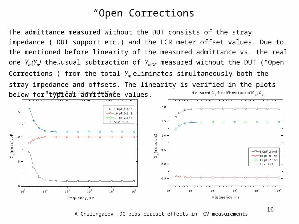
“Open Corrections”
The admittance measured without the DUT consists of the stray impedance ( DUT support etc.)
and the LCR meter offset values. Due to the mentioned before linearity of the measured
admittance vs. the real one Ym(Ya) the usual subtraction of YmOC measured without the DUT
(“Open Corrections”) from the total Ym eliminates simultaneously both the stray impedance and
offsets. The linearity is verified in the plots below for typical admittance values.
101 102 103 104 105 106
0
5
10
15
Cp(m
ea
s), p
F
Frequency, Hz
1.0pF,2.0nS10 pF,0.1nS11 pF,2.1nSSum 1+2
Measured Cp for different actual C
p, G
p
101 102 103 104 105 106
-0.5
0.0
0.5
1.0
1.5
2.0
Gp(m
ea
s), n
S
Frequency, Hz
1.0pF,2.0nS10 pF,0.1nS11 pF,2.1nSSum 1+2
Measured Gp for different actual C
p, G
p

A.Chilingarov, DC bias circuit effects in CV measurements17
Cp and Gp measured for an empty support board with the full DC bias circuit (two independent
runs) and with disconnected resistors. The similarity between the latter and the former shows
that the results are dominated by the LCR meter offsets. Note the very fine y-scale in both plots.
4. Experimental results
101 102 103 104 105
-0.35
-0.30
-0.25
-0.20
-0.15
-0.10
-0.05
0.00
0.05
0.10
0.15
With ECRun1Run2
No EC
Cp for an empty board with and without external circuit (EC)
Cp (
pF
)
Frequency (Hz)
101 102 103 104 105
-0.60
-0.55
-0.50
-0.45
-0.40
-0.35
-0.30
-0.25
-0.20
-0.15
-0.10
Gp for an empty board with and without external circuit (EC)
Gp (
nS)
Frequency (Hz)
With ECRun1Run2
No EC

A.Chilingarov, DC bias circuit effects in CV measurements18
101 102 103 104 105
8.2
8.4
8.6
8.8
9.0
9.2
9.4
9.6
9.8
10.0
10.2
Measured with no EC full EC
Reconstructed from the full EC
Cp for 10pF capacitor with and without external circuit (EC)
Cp (
pF
)
Frequency (Hz)
101 102 103 104 105
-1
0
1
2
3
4
5
Measured with no EC full EC
Reconstructed from the full EC
Gp (
nS
)
Frequency (Hz)
Gp for 10pF capacitor with and without external circuit (EC)
Cp and Gp measured for a 10 pF test capacitor with the full DC bias circuit and with disconnected
resistors. The latter gives the actual admittance which is successfully reconstructed from the
measured values. Note the conductance increase at high frequency due to the AC losses in the
capacitor.

A.Chilingarov, DC bias circuit effects in CV measurements19
Very similar results were obtained for a 100 pF test capacitor. Note the large shifts in measured
parameters successfully eliminated by the reconstruction procedure.
101 102 103 104 105
80
81
82
83
84
85
86
87
88
89
90
91
92
93
94
95
96
97
Cp for 100pF capacitor with and without external circuit (EC)
Measured with full EC no EC
Reconstructed from the full EC
Cp (
pF
)
Frequency (Hz)
101 102 103 104 105
-6
-4
-2
0
2
4
6
8
10
12Measured with
full EC no EC
Reconstructed from the full EC
Gp for 100pF capacitor with and without external circuit (EC)
Gp (
nS
)
Frequency (Hz)

A.Chilingarov, DC bias circuit effects in CV measurements20
The same 100 pF test capacitor measured with RL=10 k. The shifts in measured parameters are
very large and the reconstruction is less accurate especially at lowest frequencies.
101 102 103 104 105
0
10
20
30
40
50
60
70
80
90
100
Cp for 100pF capacitor with and without external circuit (EC)
Measured with full EC no EC
Reconstructed from the full EC
Cp (
pF
)
Frequency (Hz)
RL= 10k
101 102 103 104 105
-100
-80
-60
-40
-20
0
20
RL= 10k
Measured with full EC no EC
Reconstructed from the full EC
Gp for 100pF capacitor with and without external circuit (EC)
Gp (
nS
)
Frequency (Hz)

A.Chilingarov, DC bias circuit effects in CV measurements21
The same 10 pF test capacitor as above in parallel with a 10 M resistor. Note very large
deviations in the measured Cp from the actual 10 pF. The reconstruction works reasonably well for
both Cp and Gp.
101 102 103 104 105
0
50
100
150
200
250
300
350
Measured withno EC (no 10M) full EC
Reconstructed from the full EC
Cp for 10pF parallel to 10 M with and without external circuit (EC)
Cp (
pF)
Frequency (Hz)
101 102 103 104 105
80
84
88
92
96
100
104
Measured with no EC full EC
Reconstructed from the full EC
Gp (
nS
)
Frequency (Hz)
Gp for 100M parallel to 10pF with and without external circuit (EC)

A.Chilingarov, DC bias circuit effects in CV measurements22
5. Conclusions
1. When biasing of the tested device (DUT) during CV measurement is
provided by an external DC circuit and the capacitors are used to
decouple the input of the LCR meter from the DC potential, the
measured DUT parameters may differ significantly from their actual
values.
2. The effects disappear (apart from the shift in Gpm) when RC>10 for
the minimum RC, but in some situations RC>100 may be needed.
3. The actual DUT parameters can be reconstructed from the measured
values. However for large corrections the reconstruction accuracy
may deteriorate due to insufficient precision of the circuit description.

A.Chilingarov, DC bias circuit effects in CV measurements23
4. Tests with several known typical impedances (with and without the
external circuit) in the whole range of the frequencies planned to be
used are strongly recommended during commissioning of the CV set-
up.
5. It is better to make “Open Corrections” off-line than to subtract them
at the hardware level. In this way one can see explicitly what the
corrections are and how reproducible are they.
6. In all our results the frequency of 10 kHz is high enough to eliminate
DC bias circuit effects for capacitance.
Conclusions (continued)