db27 transfer characteristics and delay time …cgibp.com/data/lab_manual/transfer characteristics...
TRANSCRIPT

DB27 Transfer Characteristics and Delay Time Estimation of TTL and CMOS Inverters
Operating Manual Ver.1.1
An ISO 9001 : 2000 company
94-101, Electronic Complex Pardesipura, Indore- 452010, India Tel : 91-731- 2570301/02, 4211100 Fax: 91- 731- 2555643 e mail : [email protected] Website : www.scientech.bz Toll free : 1800-103-5050

DB27
Scientech Technologies Pvt. Ltd. 2

DB27
Scientech Technologies Pvt. Ltd. 3
RoHS Compliance
Scientech Products are RoHS Complied. RoHS Directive concerns with the restrictive use of Hazardous substances (Pb, Cd, Cr, Hg, Br compounds) in electric and electronic equipments. Scientech products are “Lead Free” and “Environment Friendly”. It is mandatory that service engineers use lead free solder wire and use the soldering irons upto (25 W) that reach a temperature of 450°C at the tip as the melting temperature of the unleaded solder is higher than the leaded solder.
Transfer Characteristics and Delay Time Estimation of TTL and CMOS Inverters
DB27 Table of Contents
1. Introduction 4
2. Theory 5 3. Experiments
4. Experiment 1 10 • To draw the transfer characteristics of a TTL inverter of 74LSxx series • To find the noise margins of a TTL inverter of 74LSXX series • To estimate the Delay Time of a TTL inverter of 74LSXX series.
5. Experiment 2 14 • Obtain the transfer characteristics of a TTL Schmitt Trigger
inverter of 74LSXX series. 6. Experiment 3 15
• To draw the transfer characteristics of a CMOS inverter of CD40XX series
• To find the noise margins of a CMOS inverter of CD40XX series.
• To estimate the Delay Time of a CMOS inverter of CD40XX series. 7. Experiment 4 17
• Obtain the transfer characteristics of a TTL Schmitt Trigger inverter of CD40XX series.
8. Data Sheet 18 9. Warranty 23
10. List of Accessories 23

DB27
Scientech Technologies Pvt. Ltd. 4
Introduction DB27 is a compact, easy to use digital logic experiment board. At least seven experiments can be performed on this board viz. transfer characteristics of TTL, CMOS, Schmitt trigger inverters and gate delay estimation of TTL & CMOS inverters. This board is especially designed to be used with Scientech Digital Lab ST2611 which has built in fixed and variable DC power supplies, clock source , logic high and low input facility with output indicators, logic probe, seven segment LEDs for direct readings. List of boards :
Model Name DB01 Logic Gates DB02 Universal Gate- NAND/NOR DB03 EX-OR Gate Implementation DB04 Demorgan's Theorem DB05 EX-OR Gate Application DB06 Code Conversion (Binary to Gray & Gray to Binary) DB07 Code Conversion (BCD to Excess-3 code) DB08 Binary Adder -Subtractor DB09 Encoder – Decoder DB10 Multiplexer – Demultiplexer DB11 Flip-Flops (R-S, D, J-K, T) DB12 Shift Register (4 bit SIPO) DB13 4 Bit Synchronous Binary Counter DB16 Digital to Analog Converter (R-2R ladder) DB15 BCD to 7- Segment Decoder DB17 3 Digit Event Counter DB21 Fiber Optic Digital Link DB22 Analog to digital converter (Counter Type) DB28 Monostable Multivibrator DB29 CMOS and Crystal Oscillator DB30 Adder/ Subtracter (4-Bit/8-Bit) DB31 Decoder/Demultiplexer DB32 Modulo-N programmable counter DB35 4 BIT Shift Register
………and many more

DB27
Scientech Technologies Pvt. Ltd. 5
Theory Voltage Transfer Characteristics : The static voltage transfer characteristic of a logic gate is simply a plot of the gate output voltage VOUT versus the gate input voltage VIN. We can mathematically describe the transfer characteristic as VOUT = f (VIN). We use the word static to describe the transfer characteristic because it represents behavior in response to slowly changing signals so that dynamic effects such as the delaying of the signal from gate input to gate output are avoided in measurements. Figure 1-(a) shows an ideal static transfer characteristic for an inverter with input VIN, output VOUT and power supply voltage VCC. What can we learn from a static transfer characteristic that is useful in characterizing gate operation? In order to answer this question, we need to define some terminology. First, we will consider the operating points for the inverter. These points correspond to the High and Low values on the outputs of the inverter. Since the output voltage depends on the input voltage, to find the value of the High operating point for an inverter output, the value of the Low operating point for the same inverter needs to be applied to its input. Likewise, to find the value of the Low operating point, the value of the High operating point needs to be applied. This requires that we know the values we are trying to determine! By analytically using feedback, we can combine the transfer characteristics of two identical inverters to achieve this dependency relationship.
Transfer Characteristic and Operating Points
Figure 1

DB27
Scientech Technologies Pvt. Ltd. 6
Transfer Characteristic and Operating Points
Figure 2 This is done by connecting two inverters in a loop as shown in Figure 1(b). For the two inverters, we note that VIN2 = VOUT1 and VIN1 = VOUT2. Since both of the inverters have the same transfer characteristic, we take the transfer characteristic of inverter 2 and mirror it about the VOUT = VIN line so that its VIN axis lies coincident with the VOUT axis of the transfer characteristic for inverter 1 as shown in Figure. 1(b); then the VIN axis of gate 1 also coincides with the VOUT axis of gate 2. By this mirroring operation, the relationships given in Figure 1(b) are satisfied on the axes of the plot. Because of the voltage equalities, the only points where both static transfer characteristics can be satisfied on this plot are where they intersect. These intersection points are (VIN1 = 0.15V, VOUT1= 4.05V), (VIN1 = 1.50V, VOUT1 = 1.50V), and (VIN1 = 4.05V, VOUT1 = 0.15V); these operating points are marked with OP (numerical values are taken for example). A small change in VIN1 from 1.5V will cause departure from the (VIN1 = 1.5V, VOUT1 = 1.5V) point toward one of the other two points. Thus, this point is unstable, will not persist, and is of little interest. Small departures from the other two operating points, however, are reversible and with the appropriate change in VIN1 will result in a return to those points. These are stable operating points for the inverters. They define the voltage values that correspond to High and Low on inputs and outputs of this particular inverter. Since we are using positive logic, High corresponds to 1 and Low corresponds to 0. Thus for the given inverter, the voltage values for 0 and 1 are 0.15V and 4.05V, respectively. For VOUT, the Low value is V output LOW, denoted VOL, and the High value, V output high, denoted VOH. So, for this inverter, VOL is 0.15V and VOH is 4.05V. Finally, since the Low value on the input produces a High value on the output and vice-versa, an inversion of the voltage values has occurred. For either positive or negative logic, the inverter is also often called a Not gate since it negates the input value to produce the output value.

DB27
Scientech Technologies Pvt. Ltd. 7
Noise Margins : Next, we define the concept of noise margins. Noise is assumed to be an effective voltage on one or more inputs to a gate that is added to or subtracted from the voltage normally present. The normal voltage is a stable operating point voltage. Examples of sources of noise are fluctuations in the power supply voltage VCC, noise generated by other digital circuits changing values rapidly, or external electromagnetic radiation. Intuitively, noise margins represent the amount of effective noise voltage that can be tolerated on an input without seriously disturbing the gate output.
Noise Margins and Logic Family Transfer Characteristics
Figure 3 In order to evaluate the noise margins, we need to define two additional voltages from the transfer characteristic. These are the two input voltages at which dVOUT/dVIN = – 1. The lower of these two voltages is V input Low denoted by VIL, and the higher is V input high denoted by VIH. These voltages are chosen somewhat arbitrarily as the highest value that will act as a Low input and the lowest value that will act as a High input. Intuitively, this makes some sense in that if any voltage between these two voltages is applied to the input, any noise superimposed on that voltage produces a larger noise voltage on the output, i.e., the noise voltage is amplified. This amplification of noise is interpreted as a serious disturbance of the gate output. For the inverter in Figure 1, VIL = 0.90V and VIH = 1.70V. With these two values plus VOH and VOL, we can define the static voltage noise margins for a logic gate. The Low noise margin, is NML = VIL – VOL, and the High noise margin is NMH =VOH – VIH. Static again means that dynamic effects are ignored and implies that the margins may not apply for high frequency noise. For the inverter transfer characteristic in Figure 1 (a), the noise margins are NML = 0.90 – 0.15 = 0.75V and NMH = 4.05 – 1.70 = 2.35V. The intuitive implication of these values is that:

DB27
Scientech Technologies Pvt. Ltd. 8
1. An input noise voltage of 0.75V added to input VOL gives an output that would still be interpreted as a High, and
2. An input noise voltage of 2.35V subtracted from input value VOH gives an output that would still be interpreted as a Low. Now we can consider fully the question: ‘‘what is logic 0 and what is logic 1 (for positive logic)?’’ For the inverter just analyzed, a 0 on an output has value 0.15V and a 1 on an output has a value of 4.05V. However, on the input, any voltage between GND and 0.90V is logic 0 and any voltage between 1.70V and VCC is logic 1. This is shown pictorially in Figure 2(a).
So we have defined the physical meaning of 0 and 1 in terms of voltages values and ranges. In general, these physical values are specified for an entire family of gates, for many different production lots, for different loading on the outputs, for variation in the power supply values, and for a broad range of operating temperatures. The results are a large number of transfer characteristics which collectively might appear as in Figure 2(b). From this collection of curves, we find the range of values which appears on the outputs and the range of values that can act as valid inputs by using the same techniques as employed for the individual characteristic in Figure 1 and take the worst case values for each voltage. The end result, as illustrated in Figure 2(c), is the definition of logic 0 and logic 1 for the entire family of gates. We note that in this case, with all of the variations taken into account, the noise margins become smaller than for the individual gate.
Gate Delay : Here we consider two primary gate delay parameters. In order to define these parameters, we will use an inverter as an example. We will assume that a pulse is applied to the inverter input VIN as shown in Figure 3. The response to this pulse on the output of the inverter is VOUT, also shown in Figure 3. The two parameters are the high-to-low propagation time, tPHL and the low-to-high propagation time, tPLH. We make both of these timing parameter measurements at the 50% level on the waveforms for VIN and VOUT. Formally, the 50% level is defined as the voltage 0.5(VOH – VOL) + VOL. tPHL is the time measured from this voltage on the rising input waveform to the same voltage on the falling output waveform. tPLH is the Time measured from this voltage on the falling input waveform to the same voltage on the rising output waveform.

DB27
Scientech Technologies Pvt. Ltd. 9
Gate Delay Parameter Definitions
Figure 4 Note that the subscripts on these parameters refer to the direction of change on the output waveform. These two gate delay times are defined graphically on the waveforms in Figure 4. In addition, we define a secondary parameter, the worst case propagation delay, tPD = Maximum (tPHL, tPLH). It should be noted that the 50% level for measuring delay is not universally used. For example, some manufacturers use 1.3V as the level for delay measurement for Low Power Schottky Transistor-Transistor Logic (LSTTL). Also, tPD does not universally represent the maximum propagation delay for a single gate. Some text authors use tPD to represent the average of tPHL and tPLH; we will call this tPD (average). Returning to tPD for the case of many inverters of the same type, we are taking the worst case (maximum) values that can possibly occur for each of tPHL and tPLH and then taking the maximum of these two values. The end result, tPD, is the longest delay that can ever occur for a signal change propagating from an input of a gate to the output of the gate, regardless of the direction of the signal changes. These same parameters can also be defined from a given input to a given output of more complex integrated circuits or parts thereof.

DB27
Scientech Technologies Pvt. Ltd. 10
Experiment 1 Objective : 1. To draw the transfer characteristics of a TTL inverter of 74LSxx series. 2. To find the Noise Margins of a TTL inverter of 74LSXX series. 3. To estimate the Delay Time of a TTL inverter of 74LSXX series. Equipments Needed : 1. Digital lab, ST2611. 2. DB27 digital logic board.
3. Patch cords 4. CRO
5. Signal Generator 6. Two Digital Multimeters
Circuit diagram :
Setup for Finding Transfer Characteristics
Figure 5

DB27
Scientech Technologies Pvt. Ltd. 11
Procedure : 1. Verify that the power supply to the Digital Lab ST2611 is switched off.
2. Place the logic board DB27 at the place provided on the digital lab board. 3. Take a Note of the fact that DB27 comprises of devices from two logic families
viz. TTL and CMOS and hence different power supplies and different input voltage facilities are given on this board and these two classes are separated by a horizontal dotted line for clarification. Out of the two supply input given on the board, one (5Vcc) is for TTL devices and the other one (3-15V) is for CMOS devices.
Voltage Transfer Characteristics : 1. Make the connection as shown in the Figure above. 2. Now increase the input voltage in small steps using pot P1 and note down the
corresponding values of the output voltage. 3. Draw the graph between input voltage and the output voltage. To get a fine
shape of the transfer curve at the knees take sufficient point for your observation near the transition region and then draw the graph between input and output voltages. This is the required voltage transfer characteristics for a TTL inverter of 74LSXX series.
VTC Observation On CRO : You can also directly view the complete transfer curve on your CRO screen. Follow the following steps: 1. Switch off the power supply to the board. Then connect the input of the inverter
to a triangular wave generator and also take care of the fact that the maximum amplitude of the triangular input should not exceed the maximum limits of the device under test. For TTL inverter the maximum amplitude of the triangular input should be kept between 4-5Volts
2. Connect this same input to the X-channel of the CRO and connect the other CRO input i.e. Y-channel to the output of the inverter and press XY mode switch of CRO. You will observe the complete transfer characteristics on the CRO screen. If however the view is not symmetrical or not in expected shape then just adjust the settings of CRO to get the clear picture. Also you can change the input triangular wave amplitude within tolerable limits to get the perfect view of the VTC.

DB27
Scientech Technologies Pvt. Ltd. 12
Finding NML And NMH :
1. After obtaining the Transfer characteristics curve on the graph paper make the mirror of this curve by taking the VOUT axis as independent axis and VIN axis as dependent axis and then draw the mirrored graph on the same sheet as suggested by the Figure 1.
2. These two curves will intersect each other at three points, out of which two points are the stable points marked as OP in Figure 1.and one unstable point. These two stable points correspond to the two stable states of the inverter. Mark the reflections of these points on vertical axes as VOH and VOL and they denote the output high and output low of the particular inverter.
3. Obtain the points of unity slope on the original curve and mark their reflections on the horizontal axis as VIL and VIH which represent the maximum limit of the low input and minimum limit of the high input (Figure 1.).
4. Calculate the values of High Noise Margin NMH, Low Noise Margin NML and Transition Period using the following formulae:
NMH = VOH-VIH,
NML = VOL-VIL Transition Period = VIH-VIL
Estimation of Gate Delay : To estimate the gate delay of a TTL inverter, five inverters are connected back to back on DB27 in order to provide a delay to an input in such an amount which can be appreciated over any 20MHz oscilloscope generally available in every electronics lab. Follow the procedure given below: 1. Apply a square wave of 100 KHz frequency and 5volt peak to peak voltage at
the input of the inverter chain i.e. at A3 and also apply this same input to the CRO X – channel. Connect the output of the inverter chain to the CRO Y-input and run the CRO in dual mode.
2. Now get the two stable waveforms on the CRO screen for both input and output of the inverter chain. Keep the Time/div. switch fully clockwise i.e. at the lowest value of time per division. Try to superimpose these waveforms over each other keeping their magnitude equal.
3. Now press the X5 magnifying tab on the CRO to get a magnified view of the two voltages especially near the transition region. However, if your CRO is not having high bandwidth, you may not be able to appreciate the time delay. So it is instructive here to use high bandwidth CRO or better a digital storage Oscilloscope.
4. Observe the time difference between the two waveforms at the points at which the two waves are crossing the 50% mark of their maximum amplitudes as illustrated in Figure 4. Accordingly there are two delay time values- TPHL and TPLH. (One for rising edge and one for falling edge).

DB27
Scientech Technologies Pvt. Ltd. 13
5. Calculate the actual value of these time differences by dividing them by a factor of 5 so as to compensate for magnification.
6. The values of TPHL and TPLH so obtained are the delay time values for five inverters together. So the value of delay time for a single inverter can be estimated as
tphl= TPHL/5 ; tplh= TPLH/5 :
Calculate the average value of the delay time as: TD
= (tphl + tplh)/2

DB27
Scientech Technologies Pvt. Ltd. 14
Experiment 2 Objective : Obtain the transfer characteristics of a TTL Schmitt Trigger inverter of 74LSXX series. Equipments Needed : 1. Digital lab, ST2611. 2. DB27 digital logic board.
3. Patch cords 4. CRO
5. Two Digital Multimeter Circuit diagram :
Figure 6
Procedure : 1. Connect point A to A2 and point C2 to C/D point at the output.
2. Also connect these input and output voltage socket to the two digital multimeters to record the input voltage and corresponding output voltage.
3. Use the steps explained already in the experiment 1 to draw VTC on the graph paper and observe the Voltage Transfer Characteristics on CRO as well.

DB27
Scientech Technologies Pvt. Ltd. 15
Experiment 3 Objective : 1. To draw the transfer characteristics of a CMOS inverter of CD40XX
series. 2. To find the noise margins of a CMOS inverter of CD40XX series. 3. To estimate the Delay Time of a CMOS inverter of CD40XX series. Equipments Needed : 1. Digital lab, ST2611. 2. DB27 digital logic board. 3. Patch cords 4. CRO 5. Signal Generator 6. Two Digital Multimeters
Circuit diagram :
Figure 7

DB27
Scientech Technologies Pvt. Ltd. 16
Procedure : 1. Verify that the power supply to the Digital Lab ST2611 is switched off.
2. Place the logic board DB27 at the place provided on the digital lab board. 3. Take a note of the fact that now in this experiment you will have to use 3-15Volt
power supply, i.e. you can use any of the value between 3 to 15volt for power supply. So connect this supply input pin to the variable power supply outlet on the Digital Lab ST2611. But while performing or collecting the data for a single experiment do not change power supply value.
Voltage Transfer Characteristics : Connect the Pot P2 to the input of the CD4069 inverter gate and output of this gate to the output node on the board. Also connect these points to the DMMs to record the input and output values as shown in the setup Figure given above.
Repeat the procedure as given in the experiment 1 step by step to perform this experiment as well. The only changes you can expect here is that you have to repeat the entire experiment for different power supply values. Take the readings for 5volt, 10volt and 15volt power supply ranges to appreciate some substantial change and plot the corresponding curves on the same graph sheet. Another change you can expect here is the change in the value of the delay time. Due to the capacitive loadings, the response of these gates to the fast varying signals is a bit slow in the comparison to TTL logic gates.

DB27
Scientech Technologies Pvt. Ltd. 17
Experiment 4 Objective : Obtain the transfer characteristics of a TTL Schmitt Trigger inverter of CD40XX series. Equipments Needed : 1. Digital Lab, ST2611. 2. DB27 digital logic board.
3. Patch cords 4. CRO
5. Two Digital Multimeter
Circuit diagram :
Figure 8
Procedure : 1. Connect the point B to the B2 and point D2 to C/D point at the output.
2. Also connect these input and output voltage socket to the two Digital multimeters to record the input voltage and corresponding output voltage.
3. Use the steps explained already in the experiment-1 to draw VTC on graph paper and observe the Voltage Transfer Characteristics on CRO as well.

DB27
Scientech Technologies Pvt. Ltd. 18
Data Sheet
SN74LS04-HEX INVERTER

DB27
Scientech Technologies Pvt. Ltd. 19
SN74LS04-HEX INVERTER
SN74LS14-HEX SCHMITT TRIGGER INVERTER

DB27
Scientech Technologies Pvt. Ltd. 20
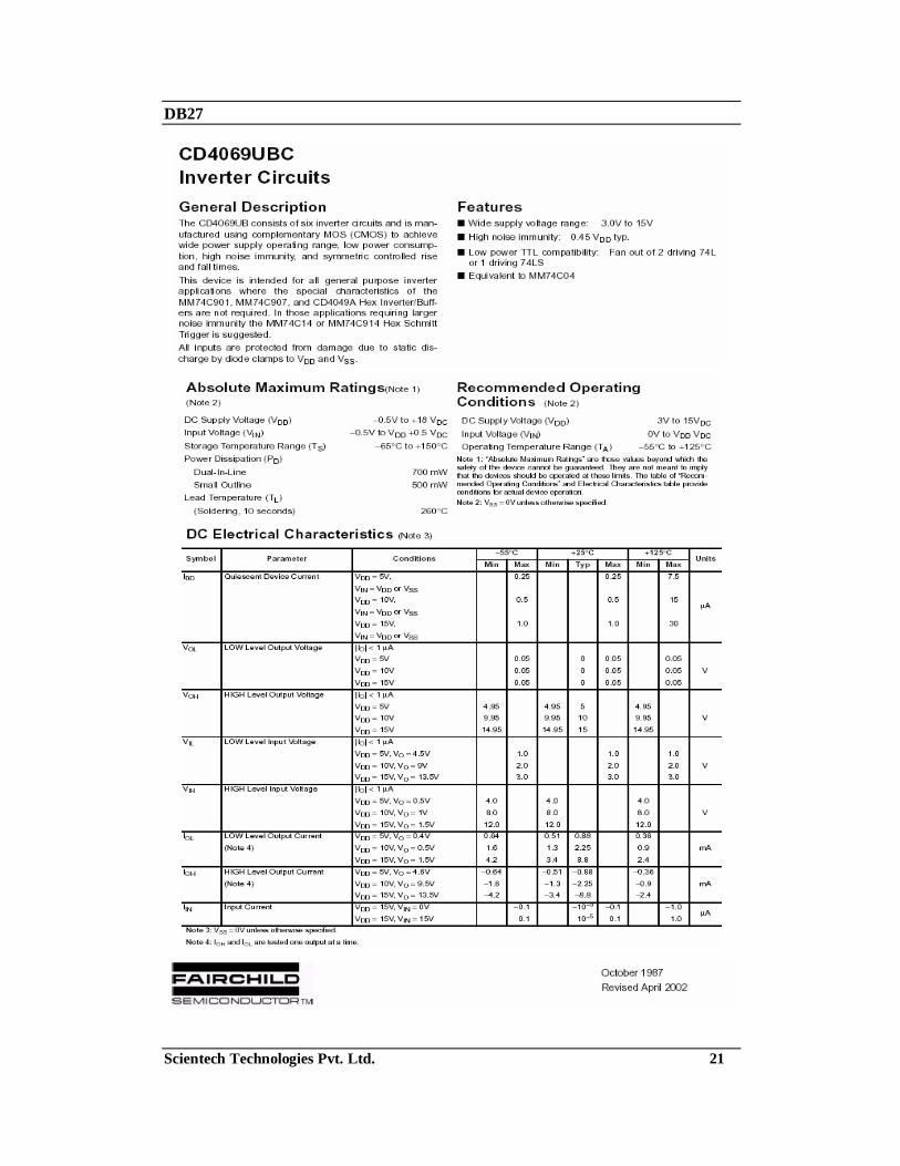
DB27
Scientech Technologies Pvt. Ltd. 21

DB27
Scientech Technologies Pvt. Ltd. 22

DB27
Scientech Technologies Pvt. Ltd. 23
Warranty 1. We guarantee the product against all manufacturing defects for 24 months from
the date of sale by us or through our dealers. Consumables like dry cell etc. are not covered under warranty.
2. The guarantee will become void, if
a) The product is not operated as per the instruction given in the operating manual.
b) The agreed payment terms and other conditions of sale are not followed.
c) The customer resells the instrument to another party. d) Any attempt is made to service and modify the instrument.
3. The non-working of the product is to be communicated to us immediately giving full details of the complaints and defects noticed specifically mentioning the type, serial number of the product and date of purchase etc.
4. The repair work will be carried out, provided the product is dispatched securely packed and insured. The transportation charges shall be borne by the customer.
For any Technical Problem Please Contact us at [email protected]
List of Accessories
1. 2 mm Patch Cords (Red) ...................................................................... 2 Nos. 2. 2 mm Patch Cord (Black) .......................................................................1 No. 3. 2 mm Patch Cord (Blue) ....................................................................... 7 Nos.
4. e-Manual.................................................................................................1 No.
Updated 26-02-2009