datos datashet
DESCRIPTION
electronicaTRANSCRIPT

7/16/2019 datos datashet
http://slidepdf.com/reader/full/datos-datashet 1/36
CoolSET™-F2ICE2A0565/165/265/365
ICE2B0565/165/265/365
ICE2A0565GICE2A0565Z
ICE2A180Z/280Z
ICE2A765I/2B765I
ICE2A765P2/2B765P2
Off-L ine SMPS Current Mode
Control ler wi th integrated 650V/
800V CoolMOS™
P o w e r M a n a g e m e n t & S u p p l y
Datasheet , V2 .0 , 11 Jun 2004
7/16/2019 datos datashet
http://slidepdf.com/reader/full/datos-datashet 2/36
Edition 2004-06-11
Published by Infineon Technologies AG, St.-Martin-Strasse 53, D-81541 München
© Infineon Technologies AG 1999. All Rights Reserved.
Attention please!
The information herein is given to describe certain components and shall not be considered as warranted char-acteristics.
Terms of delivery and rights to technical change reserved.
We hereby disclaim any and all warranties, including but not limited to warranties of non-infringement, regardingcircuits, descriptions and charts stated herein.
Infineon Technologies is an approved CECC manufacturer.
Information
For further information on technology, delivery terms and conditions and prices please contact your nearestInfineon Technologies Office in Germany or our Infineon Technologies Representatives worldwide (see addresslist).
Warnings
Due to technical requirements components may contain dangerous substances. For information on the types inquestion please contact your nearest Infineon Technologies Office.
Infineon Technologies Components may only be used in life-support devices or systems with the express writtenapproval of Infineon Technologies, if a failure of such components can reasonably be expected to cause the failureof that life-support device or system, or to affect the safety or effectiveness of that device or system. Life support
For questions on technology, delivery and prices please contact the Infineon Technologies Offices in Germany orthe Infineon Technologies Companies and Representatives worldwide: see our webpage at http:// www.infineon.com.
CoolMOS™, CoolSET™ are trademarks of Infineon Technologies AG.
CoolSET™-F2
Revision History: 2004-06-11 Datasheet
Previous Version:
Page Subjects (major changes since last revision)
7/16/2019 datos datashet
http://slidepdf.com/reader/full/datos-datashet 3/36
CoolSET™-F2
P-TO220-6-46 P-TO220-6-47P-TO220-6-47P-TO220-6-46
P-DIP-8-4, -6
P-DIP-7-1P-DIP-7-1
P-DIP-8-6
P-DSO-16/12
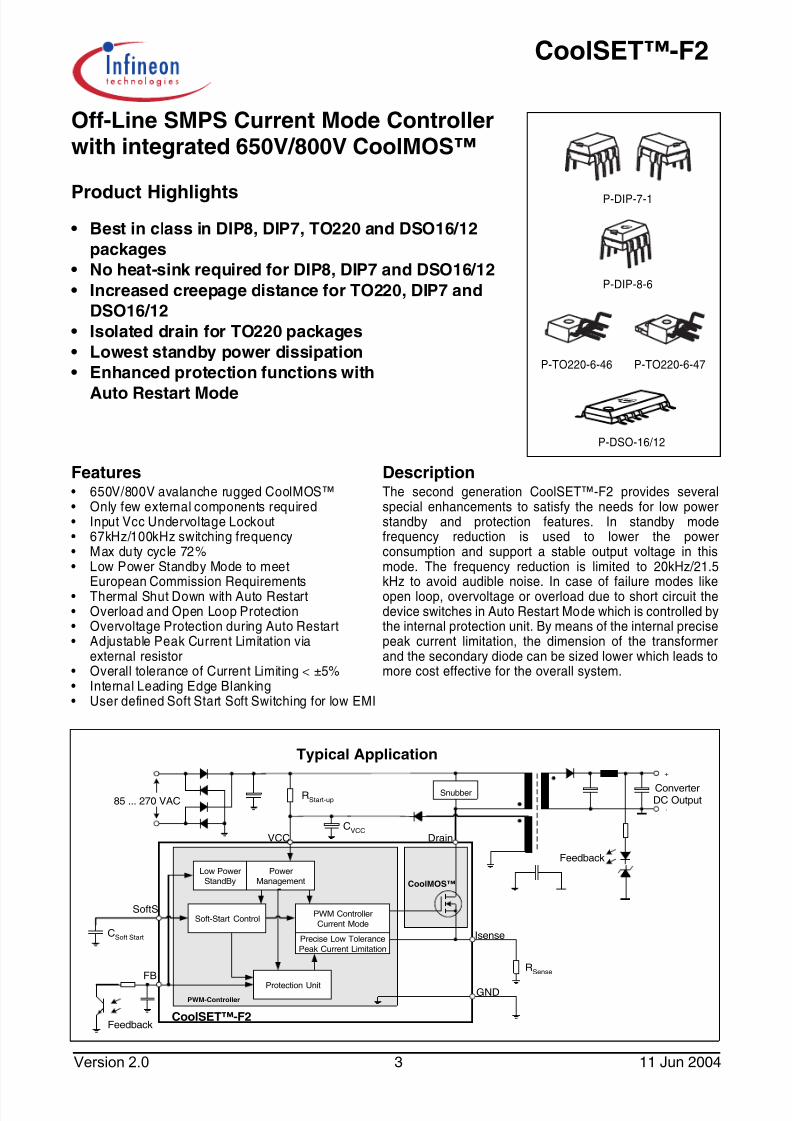
Product Highlights
• Best in class in DIP8, DIP7, TO220 and DSO16/12
packages
• No heat-sink required for DIP8, DIP7 and DSO16/12
• Increased creepage distance for TO220, DIP7 and
DSO16/12
• Isolated drain for TO220 packages
• Lowest standby power dissipation
• Enhanced protection functions with
Auto Restart Mode
CSoft Start
CVCC
RStart-up
VCC
-
ConverterDC Output
+
CoolSET™-F2
Snubber
PowerManagement
Protection Unit
Soft-Start ControlPWM Controller
Current Mode
FB
85 ... 270 VAC
Drain
Feedback
Typical Application
CoolMOS™
PWM-Controller
Low PowerStandBy
Precise Low Tolerance
Peak Current Limitation
RSense
Isense
GND
SoftS
DescriptionThe second generation CoolSET™-F2 provides severalspecial enhancements to satisfy the needs for low powerstandby and protection features. In standby modefrequency reduction is used to lower the powerconsumption and support a stable output voltage in thismode. The frequency reduction is limited to 20kHz/21.5kHz to avoid audible noise. In case of failure modes likeopen loop, overvoltage or overload due to short circuit thedevice switches in Auto Restart Mode which is controlled bythe internal protection unit. By means of the internal precisepeak current limitation, the dimension of the transformerand the secondary diode can be sized lower which leads tomore cost effective for the overall system.
Off-Line SMPS Current Mode Controllerwith integrated 650V/800V CoolMOS™
Features• 650V/800V avalanche rugged CoolMOS™• Only few external components required• Input Vcc Undervoltage Lockout• 67kHz/100kHz switching frequency• Max duty cycle 72%• Low Power Standby Mode to meet
European Commission Requirements• Thermal Shut Down with Auto Restart• Overload and Open Loop Protection• Overvoltage Protection during Auto Restart• Adjustable Peak Current Limitation via
external resistor• Overall tolerance of Current Limiting < ±5%• Internal Leading Edge Blanking• User defined Soft Start Soft Switching for low EMI

7/16/2019 datos datashet
http://slidepdf.com/reader/full/datos-datashet 4/36
CoolSET™-F2
Ordering Codes
Type Ordering Code Package VDS
FOSC
RDSon
1)
1) typ @ T=25°C
230VAC ±15%2)
2) Maximum power rating at Ta=75°C, T j=125°C and with copper area on PCB = 6cm²
85-265 VAC2)
ICE2A0565 Q67040-S4542 P-DIP-8-6 650V 100kHz 4.7Ω 23W 13W
ICE2A165 Q67040-S4426 P-DIP-8-6 650V 100kHz 3.0Ω 31W 18W
ICE2A265 Q67040-S4414 P-DIP-8-6 650V 100kHz 0.9Ω 52W 32W
ICE2A365 Q67040-S4415 P-DIP-8-6 650V 100kHz 0.45Ω 67W 45W
ICE2B0565 Q67040-S4540 P-DIP-8-6 650V 67kHz 4.7Ω 23W 13W
ICE2B165 Q67040-S4489 P-DIP-8-6 650V 67kHz 3.0Ω 31W 18W
ICE2B265 Q67040-S4478 P-DIP-8-6 650V 67kHz 0.9Ω 52W 32W
ICE2B365 Q67040-S4490 P-DIP-8-6 650V 67kHz 0.45Ω 67W 45W
ICE2A0565Z Q67040-S4541 P-DIP-7-1 650V 100kHz 4.7Ω 23W 13W
ICE2A180Z Q67040-S4546 P-DIP-7-1 800V 100kHz 3.0Ω 29W 17W
ICE2A280Z Q67040-S4547 P-DIP-7-1 800V 100KHz 0.8Ω 50W 31W
Type Ordering Code Package VDS FOSC RDSon1)
1) typ @ T=25°C
230VAC ±15%2)
2) Maximum power rating at Ta=75°C, T j=125°C and with copper area on PCB = 6cm²
85-265 VAC2)
ICE2A0565G Q67040-S4656 P-DSO-16/12 650V 100kHz 4.7Ω 23W 13W
Type Ordering Code Package VDS FOSC RDSon1)
1) typ @ T=25°C
230VAC ±15%2)
2) Maximum practical continuous power in an open frame design at Ta=75°C, T j=125°C and RthCA=2.7K/W
85-265 VAC2)
ICE2A765I Q67040-S4609 P-TO-220-6-46 650V 100kHz 0.45Ω 240W 130W
ICE2B765I Q67040-S4607 P-TO-220-6-46 650V 67kHz 0.45Ω 240W 130W
ICE2A765P2 Q67040-S4610 P-TO-220-6-47 650V 100kHz 0.45Ω 240W 130W
ICE2B765P2 Q67040-S4608 P-TO-220-6-47 650V 67kHz 0.45Ω 240W 130W

7/16/2019 datos datashet
http://slidepdf.com/reader/full/datos-datashet 5/36
CoolSET™-F2
Table of Contents Page
1 Pin Configuration and Functionality . . . . . . . . . . . . . . . . . . . . . . . . . . . . .6
1.1 Pin Configuration with P-DIP-8-6 . . . . . . . . . . . . . . . . . . . . . . . . . . . . . . . . . .61.2 Pin Configuration with P-DIP-7-1 . . . . . . . . . . . . . . . . . . . . . . . . . . . . . . . . . .6
1.3 Pin Configuration with P-TO220-6-46/47 . . . . . . . . . . . . . . . . . . . . . . . . . . . .7
1.4 Pin Configuration with P-DSO-16/12 . . . . . . . . . . . . . . . . . . . . . . . . . . . . . . .7
1.5 Pin Functionality . . . . . . . . . . . . . . . . . . . . . . . . . . . . . . . . . . . . . . . . . . . . . .8
2 Representative Blockdiagram . . . . . . . . . . . . . . . . . . . . . . . . . . . . . . . . . .9
3 Functional Description . . . . . . . . . . . . . . . . . . . . . . . . . . . . . . . . . . . . . . .10
3.1 Power Management . . . . . . . . . . . . . . . . . . . . . . . . . . . . . . . . . . . . . . . . . . .10
3.2 Improved Current Mode . . . . . . . . . . . . . . . . . . . . . . . . . . . . . . . . . . . . . . . .10
3.2.1 PWM-OP . . . . . . . . . . . . . . . . . . . . . . . . . . . . . . . . . . . . . . . . . . . . . . . . .11
3.2.2 PWM-Comparator . . . . . . . . . . . . . . . . . . . . . . . . . . . . . . . . . . . . . . . . . .11
3.3 Soft-Start . . . . . . . . . . . . . . . . . . . . . . . . . . . . . . . . . . . . . . . . . . . . . . . . . . .12
3.4 Oscillator and Frequency Reduction . . . . . . . . . . . . . . . . . . . . . . . . . . . . . .13
3.4.1 Oscillator . . . . . . . . . . . . . . . . . . . . . . . . . . . . . . . . . . . . . . . . . . . . . . . . .13
3.4.2 Frequency Reduction . . . . . . . . . . . . . . . . . . . . . . . . . . . . . . . . . . . . . . . .13
3.5 Current Limiting . . . . . . . . . . . . . . . . . . . . . . . . . . . . . . . . . . . . . . . . . . . . . .13
3.5.1 Leading Edge Blanking . . . . . . . . . . . . . . . . . . . . . . . . . . . . . . . . . . . . . .13
3.5.2 Propagation Delay Compensation . . . . . . . . . . . . . . . . . . . . . . . . . . . . . .14
3.6 PWM-Latch . . . . . . . . . . . . . . . . . . . . . . . . . . . . . . . . . . . . . . . . . . . . . . . . .143.7 Driver . . . . . . . . . . . . . . . . . . . . . . . . . . . . . . . . . . . . . . . . . . . . . . . . . . . . . .14
3.8 Protection Unit (Auto Restart Mode) . . . . . . . . . . . . . . . . . . . . . . . . . . . . . .15
3.8.1 Overload / Open Loop with Normal Load . . . . . . . . . . . . . . . . . . . . . . . .15
3.8.2 Overvoltage due to Open Loop with No Load . . . . . . . . . . . . . . . . . . . . .16
3.8.3 Thermal Shut Down . . . . . . . . . . . . . . . . . . . . . . . . . . . . . . . . . . . . . . . . .16
4 Electrical Characteristics . . . . . . . . . . . . . . . . . . . . . . . . . . . . . . . . . . . . .17
4.1 Absolute Maximum Ratings . . . . . . . . . . . . . . . . . . . . . . . . . . . . . . . . . . . . .17
4.2 Thermal Impedance (ICE2X765I and ICE2X765P2) . . . . . . . . . . . . . . . . . .19
4.3 Operating Range . . . . . . . . . . . . . . . . . . . . . . . . . . . . . . . . . . . . . . . . . . . . .194.4 Characteristics . . . . . . . . . . . . . . . . . . . . . . . . . . . . . . . . . . . . . . . . . . . . . . .20
4.4.1 Supply Section . . . . . . . . . . . . . . . . . . . . . . . . . . . . . . . . . . . . . . . . . . . . .20
4.4.2 Internal Voltage Reference . . . . . . . . . . . . . . . . . . . . . . . . . . . . . . . . . . .21
4.4.3 Control Section . . . . . . . . . . . . . . . . . . . . . . . . . . . . . . . . . . . . . . . . . . . .21
4.4.4 Protection Unit . . . . . . . . . . . . . . . . . . . . . . . . . . . . . . . . . . . . . . . . . . . . .22
4.4.5 Current Limiting . . . . . . . . . . . . . . . . . . . . . . . . . . . . . . . . . . . . . . . . . . . .22
4.4.6 CoolMOS™ Section . . . . . . . . . . . . . . . . . . . . . . . . . . . . . . . . . . . . . . . . .23
5 Typical Performance Characteristics . . . . . . . . . . . . . . . . . . . . . . . . . . .25
6 Layout Recommendation for C18 . . . . . . . . . . . . . . . . . . . . . . . . . . . . . . .31
7 Outline Dimension 32
7/16/2019 datos datashet
http://slidepdf.com/reader/full/datos-datashet 6/36
CoolSET™-F2
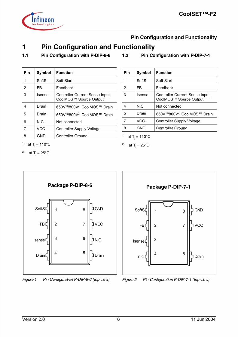
Pin Configuration and Functionality
1 Pin Configuration and Functionality1.1 Pin Configuration with P-DIP-8-6
Figure 1 Pin Configuration P-DIP-8-6 (top view)
1.2 Pin Configuration with P-DIP-7-1
Figure 2 Pin Configuration P-DIP-7-1 (top view)
Pin Symbol Function
1 SoftS Soft-Start
2 FB Feedback
3 Isense Controller Current Sense Input,CoolMOS™ Source Output
4 Drain 650V1)/800V2) CoolMOS™ Drain
1) at T j = 110°C
5 Drain 650V1)/800V2) CoolMOS™ Drain
2) at T j = 25°C
6 N.C Not connected
7 VCC Controller Supply Voltage
8 GND Controller Ground
Package P-DIP-8-6
1
6
7
8
4
3
2
5
VCCFB
Isense
Drain
SoftS
N.C
GND
Drain
Pin Symbol Function
1 SoftS Soft-Start
2 FB Feedback
3 Isense Controller Current Sense Input,CoolMOS™ Source Output
4 N.C. Not connected
5 Drain 650V1)/800V2) CoolMOS™ Drain
1) at T j = 110°C
2) at T j = 25°C
7 VCC Controller Supply Voltage
8 GND Controller Ground
1
7
8
4
3
2
5
VCCFB
Isense
n.c.
SoftS GND
Drain
Package P-DIP-7-1

7/16/2019 datos datashet
http://slidepdf.com/reader/full/datos-datashet 7/36
CoolSET™-F2
Pin Configuration and Functionality
1.3 Pin Configuration with P-TO220-6-46/47
Figure 3 Pin Configuration P-TO220-6-46/47
(top view)
1.4 Pin Configuration with P-DSO-16/12
Figure 4 Pin Configuration P-DSO-16/12 (top view)
Pin Symbol Function
1 Drain 650V1) CoolMOS™ Drain
1) at T j = 110°C
3 Isense Controller Current Sense Input,CoolMOS™ Source Output
4 GND Controller Ground
5 VCC Controller Supply Voltage
6 SoftS Soft-Start
7 FB Feedback
Package P-TO220-6-46/47
1
D r a
i n
2 3 4 5 6 7
I s e n s e
G N D
V C C
S o
f t S
F B
Pin Symbol Function
1 N.C. Not Connected
2 SoftS Soft-Start
3 FB Feedback
4 Isense Controller Current Sense Input,CoolMOS™ Source Output
5 Drain 650V1) CoolMOS™ Drain
1) at T j = 110°C
6 Drain 650V1) CoolMOS™ Drain
7 Drain 650V1) CoolMOS™ Drain
8 Drain 650V1) CoolMOS™ Drain
9 N.C. Not Connected
10 N.C. Not Connected
11 VCC Controller Supply Voltage
12 GND Controller Ground
Package P-DSO-16/12
10
11
12
9
VC CSoftS
FB
Isense
N.C
N.C.
GN D
N.C.
Drain
Drain
8
7
3
2
1
4
Drain
Drain
5
6

7/16/2019 datos datashet
http://slidepdf.com/reader/full/datos-datashet 8/36
CoolSET™-F2
Pin Configuration and Functionality
1.5 Pin Functionality
SoftS (Soft Start & Auto Restart Control)This pin combines the function of Soft Start in case ofStart Up and Auto Restart Mode and the controlling ofthe Auto Restart Mode in case of an error detection.
FB (Feedback)
The information about the regulation is provided by theFB Pin to the internal Protection Unit and to the internalPWM-Comparator to control the duty cycle.
Isense (Current Sense)
The Current Sense pin senses the voltage developedon the series resistor inserted in the source of theintegrated CoolMOS™. When Isense reaches theinternal threshold of the Current Limit Comparator, theDriver output is disabled. By this means the OverCurrent Detection is realized.
Furthermore the current information is provided for thePWM-Comparator to realize the Current Mode.
Drain (Drain of integrated CoolMOS™)
Pin Drain is the connection to the Drain of the internalCoolMOSTM.
VCC (Power supply)
This pin is the positive supply of the IC. The operatingrange is between 8.5V and 21V.
To provide overvoltage protection the driver getsdisabled when the voltage becomes higher than 16.5Vduring Start Up Phase.
GND (Ground)
This pin is the ground of the primary side of the SMPS.
7/16/2019 datos datashet
http://slidepdf.com/reader/full/datos-datashet 9/36

7/16/2019 datos datashet
http://slidepdf.com/reader/full/datos-datashet 10/36
CoolSET™-F2
Functional Description
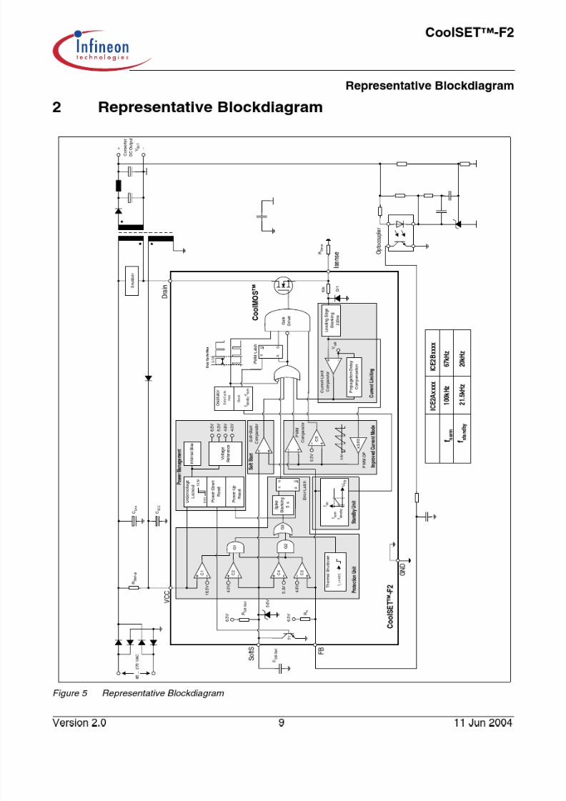
3 Functional Description
3.1 Power Management
Figure 6 Power Management
The Undervoltage Lockout monitors the externalsupply voltage VVCC. In case the IC is inactive thecurrent consumption is max. 55µA. When the SMPS isplugged to the main line the current through RStart-up
charges the external Capacitor CVCC. When VVCC
exceeds the on-threshold VCCon=13.5V the internal biascircuit and the voltage reference are switched on. Afterthat the internal bandgap generates a referencevoltage VREF=6.5V to supply the internal circuits. Toavoid uncontrolled ringing at switch-on a hysteresis isimplemented which means that switch-off is only afteractive mode when Vcc falls below 8.5V.
In case of switch-on a Power Up Reset is done byresetting the internal error-latch in the protection unit.
When VVCC falls below the off-threshold VCCoff=8.5V theinternal reference is switched off and the Power Downreset let T1 discharging the soft-start capacitor C
Soft-Startat pin SoftS. Thus it is ensured that at every switch-onthe voltage ramp at pin SoftS starts at zero.
3.2 Improved Current Mode
Figure 7 Current Mode
Current Mode means that the duty cycle is controlledby the slope of the primary current. This is done bycomparison the FB signal with the amplified currentsense signal.
Figure 8 Pulse Width Modulation
In case the amplified current sense signal exceeds theFB signal the on-time Ton of the driver is finished byresetting the PWM-Latch (see Figure 8).
The primary current is sensed by the external seriesresistor RSense inserted in the source of the integratedCoolMOS™. By means of Current Mode regulation, the
In te rn a lB ia s
Vo l ta g e
Re fe re n c e
6 .5 V
4 .8 V
Un d e rv o l ta g e
L o c k o u t
1 3 .5 V
8 .5 V
P o w e r - D o w n
R e s e t
P o w e r - U p
R e s e t
Power Management
5 .3 V
4 .0 V
T 1
PW M -Latch
R
S
Q
Q
Erro r -L a tc hSo f tS
6 .5 V
Er ro r -De te c t io n
V C C
M a in L in e (1 0 0 V-3 8 0 V)
Prim ary W ind ing
So f t -S ta r t Co m p a ra to r
C VC C
R Soft-Start
RStart-Up
CSoft-Start
x3 .65
PW M O P
Improved
Current Mode
0 .8V
PW M Co m pa rator
PW M -La tch
Isense
F BR
S
Q
Q
Driver
Sof t -S tar t C om para tor
t
FB
Amplified Current Signal
Ton
t
0.8V
Driver

7/16/2019 datos datashet
http://slidepdf.com/reader/full/datos-datashet 11/36
CoolSET™-F2
Functional Description
secondary output voltage is insensitive on linevariations. Line variation changes the currentwaveform slope which controls the duty cycle.
The external RSense allows an individual adjustment ofthe maximum source current of the integratedCoolMOS™.
Figure 9 Improved Current Mode
To improve the Current Mode during light loadconditions the amplified current ramp of the PWM-OPis superimposed on a voltage ramp, which is built bythe switch T2, the voltage source V1 and the 1st orderlow pass filter composed of R1 and C1(see Figure 9,Figure 10). Every time the oscillator shuts down formax. duty cycle limitation the switch T2 is closed byVOSC. When the oscillator triggers the Gate Driver T2 isopened so that the voltage ramp can start.
In case of light load the amplified current ramp is to
small to ensure a stable regulation. In that case theVoltage Ramp is a well defined signal for thecomparison with the FB-signal. The duty cycle is thencontrolled by the slope of the Voltage Ramp.
By means of the Comparator C5, the Gate Driver isswitched-off until the voltage ramp exceeds 0.3V. Itallows the duty cycle to be reduced continuously till 0%by decreasing VFB below that threshold.
Figure 10 Light Load Conditions
3.2.1 PWM-OP
The input of the PWM-OP is applied over the internalleading edge blanking to the external sense resistorRSense connected to pin Isense. RSense converts thesource current into a sense voltage. The sense voltageis amplified with a gain of 3.65 by PWM OP. The outputof the PWM-OP is connected to the voltage source V1.The voltage ramp with the superimposed amplifiedcurrent signal is fed into the positive inputs of the PWM-Comparator, C5 and the Soft-Start-Comparator.
3.2.2 PWM-ComparatorThe PWM-Comparator compares the sensed currentsignal of the integrated CoolMOSTM with the feedbacksignal VFB (see Figure 11). VFB is created by anexternal optocoupler or external transistor incombination with the internal pull-up resistor RFB andprovides the load information of the feedback circuitry.When the amplified current signal of the integratedCoolMOS™ exceeds the signal VFB the PWM-Comparator switches off the Gate Driver.
x3 . 65
P W M O P
0.8V1 0 kΩ
O sci l lato r
PW M C om pa rator
2 0 p F
T2
R1
C1
F B
P W M -La tch
V1
C 50 . 3V
G ate Dr ive r
Voltage Ramp
VO S C
So f t-S ta r t C om pa ra to r
t
t
VOSC
0.8V
FB
t
max.
Duty Cycle
0.3V
Gate Driver
Voltage Ramp

7/16/2019 datos datashet
http://slidepdf.com/reader/full/datos-datashet 12/36
CoolSET™-F2
Functional Description
Figure 11 PWM Controlling
3.3 Soft-Start
Figure 12 Soft-Start Phase
The Soft-Start is realized by the internal pull-up resistor
RSoft-Start and the external Capacitor CSoft-Start (seeFigure 5). The Soft-Start voltage VSoftS is generated bycharging the external capacitor CSoft Start by the internal
pull-up resistor RSoft-Start. The Soft-Start-Comparatorcompares the voltage at pin SoftS at the negative inputwith the ramp signal of the PWM-OP at the positive
input. When Soft-Start voltage VSoftS is less thanFeedback voltage VFB the Soft-Start-Comparator limitsthe pulse width by resetting the PWM-Latch (seeFigure 12). In addition to Start-Up, Soft-Start is alsoactivated at each restart attempt during Auto Restart.By means of the above mentioned CSoft-Start the Soft-Start can be defined by the user. The Soft-Start isfinished when VSoftS exceeds 5.3V. At that time theProtection Unit is activated by Comparator C4 andsenses the FB by Comparator C3 wether the voltage isbelow 4.8V which means that the voltage on thesecondary side of the SMPS is settled. The internalZener Diode at SoftS has a clamp voltage of 5.6V to
prevent the internal circuit from saturation (see Figure13).
Figure 13 Activation of Protection Unit
The Start-Up time TStart-Up within the converter outputvoltage VOUT is settled must be shorter than the Soft-Start Phase TSoft-Start (see Figure 14).
By means of Soft-Start there is an effectiveminimization of current and voltage stresses on theintegrated CoolMOS™, the clamp circuit and the outputovershoot and prevents saturation of the transformerduring Start-Up.
x3 .65
PW M O P
Improved
Current Mode
PW M Co m pa rator
I sense
So f t -Star t C om para tor6 .5V
PW M -La tch
0 .8V
F B
Optocoup le r
RF B
t
5.3V
VSof tS
Ga te D r ive r
t
TSof t -Star t
5.6V
6.5V
RF B
6.5V
Power -Up Rese t
C 45.3V
C 34.8V
RSoft-Start
F B
R
S
Q
Q
Error-Latch
R
S
Q
Q
PWM-La tch
G 2
Clock
GateDriver
5.6V
SoftS
C S o ft S t ar t – T S of t S t ar t –
RS o ft S t ar t – 1.69×
--------------------------------------=

7/16/2019 datos datashet
http://slidepdf.com/reader/full/datos-datashet 13/36
CoolSET™-F2
Functional Description
Figure 14 Start Up Phase
3.4 Oscillator and Frequency
Reduction
3.4.1 Oscillator
The oscillator generates a frequency fswitch = 67kHz/ 100kHz. A resistor, a capacitor and a current sourceand current sink which determine the frequency areintegrated. The charging and discharging current of theimplemented oscillator capacitor are internallytrimmed, in order to achieve a very accurate switchingfrequency. The ratio of controlled charge to discharge
current is adjusted to reach a max. duty cycle limitationof Dmax=0.72.
3.4.2 Frequency Reduction
The frequency of the oscillator is depending on thevoltage at pin FB. The dependence is shown in Figure15. This feature allows a power supply to operate atlower frequency at light loads thus lowering theswitching losses while maintaining good crossregulation performance and low output ripple. In caseof low power the power consumption of the wholeSMPS can now be reduced very effective. The minimal
reachable frequency is limited to 20kHz/21.5 kHz toavoid audible noise in any case.
Figure 15 Frequency Dependence
3.5 Current Limiting
There is a cycle by cycle current limiting realized by theCurrent-Limit Comparator to provide an overcurrentdetection. The source current of the integratedCoolMOSTM is sensed via an external sense resistorRSense. By means of RSense the source current istransformed to a sense voltage VSense. When thevoltage VSense exceeds the internal threshold voltageVcsth the Current-Limit-Comparator immediately turnsoff the gate drive. To prevent the Current Limiting fromdistortions caused by leading edge spikes a LeadingEdge Blanking is integrated at the Current Sense.Furthermore a Propagation Delay Compensation isadded to support the immediate shut down of theCoolMOS™ in case of overcurrent.
3.5.1 Leading Edge Blanking
Figure 16 Leading Edge Blanking
Each time when CoolMOS™ is switched on a leadingspike is generated due to the primary-sidecapacitances and secondary-side rectifier reverserecovery time. To avoid a premature termination of the
switching pulse this spike is blanked out with a timeconstant of tLEB = 220ns. During that time the output of
t
t
VSoftS
t
5.3V
4.8V
TSoft-Start
VO UT
VFB
VO UT
TStart-Up
67kHz100kHz
20kHz21.5kHz
21.5
65
100
1.0 1.1 1.2 1.3 1.4 1.5 1.6 1.7 1.8 1.9 2.0
kHz
V FB
V
f O S C
ICE2BxxxxICE2Axxxx
f norm
f standby
t
VS e n s e
Vcsth t
LE B
= 2 2 0 n s

7/16/2019 datos datashet
http://slidepdf.com/reader/full/datos-datashet 14/36
CoolSET™-F2
Functional Description
the Current-Limit Comparator cannot switch off thegate drive.
3.5.2 Propagation Delay Compensation
In case of overcurrent detection by ILimit the shut downof CoolMOS™ is delayed due to the propagation delayof the circuit. This delay causes an overshoot of thepeak current Ipeak which depends on the ratio of dI/dt ofthe peak current (see Figure 17).
.
Figure 17 Current Limiting
The overshoot of Signal2 is bigger than of Signal1 due
to the steeper rising waveform.A propagation delay compensation is integrated tobound the overshoot dependent on dI/dt of the risingprimary current. That means the propagation delaytime between exceeding the current sense thresholdVcsth and the switch off of CoolMOS™ is compensatedover temperature within a range of at least.
Figure 18 Dynamic Voltage Threshold V csth
The propagation delay compensation is done bymeans of a dynamic threshold voltage Vcsth (see Figure18). In case of a steeper slope the switch off of the
driver is earlier to compensate the delay.E.g. Ipeak = 0.5A with RSense = 2. Without propagationdelay compensation the current sense threshold is setto a static voltage level Vcsth=1V. A current ramp ofdI/dt = 0.4A/µs, that means dVSense /dt = 0.8V/µs, and apropagation delay time of i.e. tPropagation Delay =180nsleads then to a Ipeak overshoot of 12%. By means ofpropagation delay compensation the overshoot is onlyabout 2% (see Figure 19).
Figure 19 Overcurrent Shutdown
3.6 PWM-Latch
The oscillator clock output applies a set pulse to thePWM-Latch when initiating CoolMOS™ conduction.After setting the PWM-Latch can be reset by the PWM-OP, the Soft-Start-Comparator, the Current-Limit-Comparator, Comparator C3 or the Error-Latch of theProtection Unit. In case of resetting the driver is shutdown immediately.
3.7 Driver
The driver-stage drives the gate of the CoolMOS™ andis optimized to minimize EMI and to provide high circuitefficiency. This is done by reducing the switch on slopewhen reaching the CoolMOS™ threshold. This isachieved by a slope control of the rising edge at thedriver’s output (see Figure 20) to the CoolMOS™ gate.
Thus the leading switch on spike is minimized. WhenCoolMOS™ is switched off, the falling shape of thedriver is slowed down when reaching 2V to prevent anovershoot below ground. Furthermore the driver circuitis designed to eliminate cross conduction of the outputstage. At voltages below the undervoltage lockoutthreshold VVCCoff the gate drive is active low.
t
ISense
ILimit
tPropagation Delay
IOvershoot1
Ipeak1
Signal2Signal1
IOvershoot2I
peak2
0 RSense
dI peak dt
------------× dV Sense
dt ---------------≤ ≤
t
Vcsth
VOSC
Signal1 Signal2
VSense
max. Duty Cycle
off time
tPropagation Delay
0.9
0.95
1
1.05
1.1
1.15
1.2
1.25
1.3
0 0.2 0.4 0.6 0.8 1 1.2 1.4 1.6 1.8 2
with compensation without compensation
dt
dV Sense
V
V/us
V S e n s e

7/16/2019 datos datashet
http://slidepdf.com/reader/full/datos-datashet 15/36
CoolSET™-F2
Functional Description
Figure 20 Internal Gate Rising Slope
3.8 Protection Unit (Auto Restart Mode)
An overload, open loop and overvoltage detection isintegrated within the Protection Unit. These threefailure modes are latched by an Error-Latch. Additionalthermal shutdown is latched by the Error-Latch. In caseof those failure modes the Error-Latch is set after ablanking time of 5µs and the CoolMOS™ is shut down.That blanking prevents the Error-Latch from distortionscaused by spikes during operation mode.
3.8.1 Overload / Open Loop with Normal
LoadFigure 21 shows the Auto Restart Mode in case ofoverload or open loop with normal load. The detectionof open loop or overload is provided by the ComparatorC3, C4 and the AND-gate G2 (see Figure 22). Thedetection is activated by C4 when the voltage at pinSoftS exceeds 5.3V. Till this time the IC operates in theSoft-Start Phase. After this phase the comparator C3can set the Error-Latch in case of open loop or overloadwhich leads the feedback voltage VFB to exceed thethreshold of 4.8V. After latching VCC decreases till8.5V and inactivates the IC. At this time the externalSoft-Start capacitor is discharged by the internal
transistor T1 due to Power Down Reset. When the ICis inactive VVCC increases till VCCon = 13.5V by chargingthe Capacitor CVCC by means of the Start-Up ResistorRStart-Up. Then the Error-Latch is reset by Power UpReset and the external Soft-Start capacitor CSoft-Start ischarged by the internal pull-up resistor RSoft-Start. Duringthe Soft-Start Phase which ends when the voltage atpin SoftS exceeds 5.3V the detection of overload andopen loop by C3 and G2 is inactive. In this way the StartUp Phase is not detected as an overload.
Figure 21 Auto Restart Mode
Figure 22 FB Detection
t
VGate
5 V
c a . t = 130n sOverload / Open Loop with Normal Load
FB
t
4.8V
5.3V
SoftS
5µs Blanking
Failure
Detection
Soft-Start Phase
VCC
13.5V
8.5V
t
Driver
t
TRestart
TBurst1
t
R Soft-S tar t
6.5V
CSoft-S tar t
C 45.3V
C 34.8V
G 2T1
Error-Latch
Power Up Reset
RFB
6.5V
FB
SoftS

7/16/2019 datos datashet
http://slidepdf.com/reader/full/datos-datashet 16/36
CoolSET™-F2
Functional Description
But the Soft-Start Phase must be finished within theStart Up Phase to force the voltage at pin FB below thefailure detection threshold of 4.8V.
3.8.2 Overvoltage due to Open Loop with
No Load
Figure 23 Auto Restart Mode
Figure 23 shows the Auto Restart Mode for open loopand no load condition. In case of this failure mode theconverter output voltage increases and also VCC. Anadditional protection by the comparators C1, C2 andthe AND-gate G1 is implemented to consider thisfailure mode (see Figure 24).The overvoltage detectionis provided by Comparator C1 only in the first timeduring the Soft-Start Phase till the Soft-Start voltageexceeds the threshold of the Comparator C2 at 4.0Vand the voltage at pin FB is above 4.8V. When VCCexceeds 16.5V during the overvoltage detection phase
C1 can set the Error-Latch and the Burst Phase duringAuto Restart Mode is finished earlier. In that caseTBurst2 is shorter than TSoft-Start. By means of C2 the
normal operation mode is prevented from overvoltagedetection due to varying of VCC concerning theregulation of the converter output. When the voltage
VSoftS is above 4.0V the overvoltage detection by C1 isdeactivated.
Figure 24 Overvoltage Detection
3.8.3 Thermal Shut Down
Thermal Shut Down is latched by the Error-Latch when junction temperature T j of the pwm controller isexceeding an internal threshold of 140°C. In that casethe IC switches in Auto Restart Mode.
Note: All the values which are mentioned in the
functional description are typical. Please referto Electrical Characteristics for min/max limitvalues.
Open loop & no load condition
t
Driver
13.5V16.5V
F B
4.8V
5µs B lanking
Fai lureDetection
5.3V
SoftS
4.0VOvervo l tage
Detect ion P hase
Soft-Start P hase
t
t
TR e s t a r t
T B u rs t 2
VC C
8.5V
Overvoltage Detection
t
6 . 5 V
CSoft-Start
V C C
RSoft-Start
C 11 6 . 5 V
C 2
4 . 0 V
T 1
Sof tS
G 1E r r o r L a t ch
P o w e r U p R e s e t

7/16/2019 datos datashet
http://slidepdf.com/reader/full/datos-datashet 17/36
CoolSET™-F2
Electrical Characteristics
4 Electrical Characteristics
4.1 Absolute Maximum Ratings
Note: Absolute maximum ratings are defined as ratings, which when being exceeded may lead to destructionof the integrated circuit. For the same reason make sure, that any capacitor that will be connected to pin 6 ( V CC) is discharged before assembling the application circuit.
Parameter Symbol Limit Values Unit Remarks
min. max.
Drain Source VoltageICE2A0565/165/265/365/765I/765P2ICE2B0565/165/265/365/765I/765P2ICE2A0565GICE2A0565Z
V DS - 650 V T j = 110°C
Drain Source VoltageICE2A180Z/280Z
V DS - 800 V T j = 25°C
Avalanche energy,repetitive t AR limited bymax. T j=150°C1)
1) Repetitive avalanche causes additional power losses that can be calculated as P AV=E AR* f
ICE2A0565 E AR1 - 0.01 mJ
ICE2A165 E AR2 - 0.07 mJ
ICE2A265 E AR3 - 0.40 mJ
ICE2A365 E AR4 - 0.50 mJ
ICE2B0565 E AR5 - 0.01 mJ
ICE2B165 E AR6 - 0.07 mJ
ICE2B265 E AR7 - 0.40 mJ
ICE2B365 E AR8 - 0.50 mJ
ICE2A0565G E AR9 - 0.01 mJ
ICE2A0565Z E AR10 - 0.01 mJ
ICE2A180Z E AR11 - 0.07 mJ
ICE2A280Z E AR12 - 0.40 mJ
ICE2A765I E AR13 - 0.50 mJ
ICE2B765I E AR14 - 0.50 mJICE2A765P2 E AR15 - 0.50 mJ
ICE2B765P2 E AR16 - 0.50 mJ

7/16/2019 datos datashet
http://slidepdf.com/reader/full/datos-datashet 18/36
CoolSET™-F2
Electrical Characteristics
Parameter Symbol Limit Values Unit Remarks
min. max.
Avalanche current,repetitive tAR limited bymax. T j=150°C
ICE2A0565 I AR1 - 0.5 A
ICE2A165 I AR2 - 1 A
ICE2A265 I AR3 - 2 A
ICE2A365 I AR4 - 3 A
ICE2B0565 I AR5 - 0.5 A
ICE2B165 I AR6 - 1 A
ICE2B265 I AR7 - 2 A
ICE2B365 I AR8 - 3 A
ICE2A0565G I AR9 - 0.5 A
ICE2A0565Z I AR10 - 0.5 A
ICE2A180Z I AR11 - 1 A
ICE2A280Z I AR12 - 2 A
ICE2A765I I AR13 - 7 A
ICE2B765I I AR14 - 7 A
ICE2A765P2 I AR15 - 7 A
ICE2B765P2 I AR16
- 7 A
V CC Supply Voltage V CC -0.3 22 V
FB Voltage V FB -0.3 6.5 V
SoftS Voltage V SoftS -0.3 6.5 V
ISense I Sense -0.3 3 V
Junction Temperature T j -40 150 °C Controller & CoolMOS™
Storage Temperature T S -50 150 °C
Thermal ResistanceJunction-Ambient
R thJA1 - 90 K/W P-DIP-8-6
R thJA2 - 96 K/W P-DIP-7-1
R thJA3 - 110 K/W P-DSO-16/12
ESD Robustness1)
1) Equivalent to discharging a 100pF capacitor through a 1.5 kΩ series resistor
2) 1kV at pin drain of ICE2x0565, ICE2A0565Z and ICE2A0565G
V ESD - 22) kV Human Body Model

7/16/2019 datos datashet
http://slidepdf.com/reader/full/datos-datashet 19/36
CoolSET™-F2
Electrical Characteristics
4.2 Thermal Impedance (ICE2X765I and ICE2X765P2)
4.3 Operating Range
Note: Within the operating range the IC operates as described in the functional description.
Parameter Symbol Limit Values Unit Remarks
min. max.
Thermal ResistanceJunction-Ambient
ICE2A765IICE2B765IICE2A765P2ICE2B765P2
R thJA4 - 74 K/W Free standing with no heat-sink
Junction-Case ICE2A765IICE2B765IICE2A765P2ICE2B765P2
R thJC - 2.5 K/W
Parameter Symbol Limit Values Unit Remarks
min. max.
V CC Supply Voltage V CC V CCoff 21 VJunction Temperature ofController
T JCon -25 130 °C Limited due to thermal shut downof controller
Junction Temperature ofCoolMOS™
T JCoolMOS -25 150 °C
7/16/2019 datos datashet
http://slidepdf.com/reader/full/datos-datashet 20/36
CoolSET™-F2
Electrical Characteristics
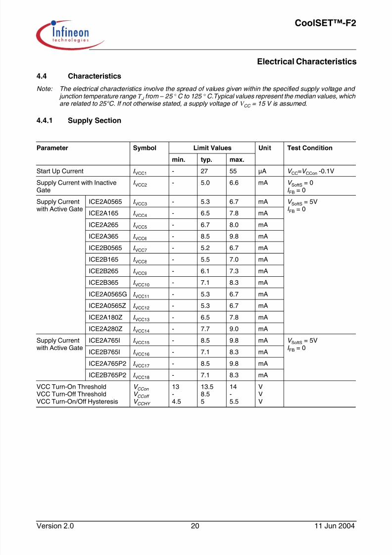
4.4 Characteristics
Note: The electrical characteristics involve the spread of values given within the specified supply voltage and
junction temperature range T J from – 25 °C to 125 °C.Typical values represent the median values, whichare related to 25°C. If not otherwise stated, a supply voltage of V CC = 15 V is assumed.
4.4.1 Supply Section
Parameter Symbol Limit Values Unit Test Condition
min. typ. max.
Start Up Current I VCC1 - 27 55 µA V CC=V CCon -0.1V
Supply Current with InactiveGate
I VCC2 - 5.0 6.6 mA V SoftS = 0I FB
= 0
Supply Currentwith Active Gate
ICE2A0565 I VCC3 - 5.3 6.7 mA V SoftS = 5VI FB = 0
ICE2A165 I VCC4 - 6.5 7.8 mA
ICE2A265 I VCC5 - 6.7 8.0 mA
ICE2A365 I VCC6 - 8.5 9.8 mA
ICE2B0565 I VCC7 - 5.2 6.7 mA
ICE2B165 I VCC8 - 5.5 7.0 mA
ICE2B265 I VCC9 - 6.1 7.3 mA
ICE2B365 I VCC10 - 7.1 8.3 mA
ICE2A0565G I VCC11 - 5.3 6.7 mA
ICE2A0565Z I VCC12 - 5.3 6.7 mA
ICE2A180Z I VCC13 - 6.5 7.8 mA
ICE2A280Z I VCC14 - 7.7 9.0 mA
Supply Currentwith Active Gate
ICE2A765I I VCC15 - 8.5 9.8 mA V SoftS = 5VI FB = 0
ICE2B765I I VCC16 - 7.1 8.3 mA
ICE2A765P2 I VCC17 - 8.5 9.8 mA
ICE2B765P2 I VCC18 - 7.1 8.3 mA
VCC Turn-On ThresholdVCC Turn-Off ThresholdVCC Turn-On/Off Hysteresis
V CCon V CCoff
V CCHY
13-4.5
13.58.55
14-5.5
VVV
7/16/2019 datos datashet
http://slidepdf.com/reader/full/datos-datashet 21/36
CoolSET™-F2
Electrical Characteristics
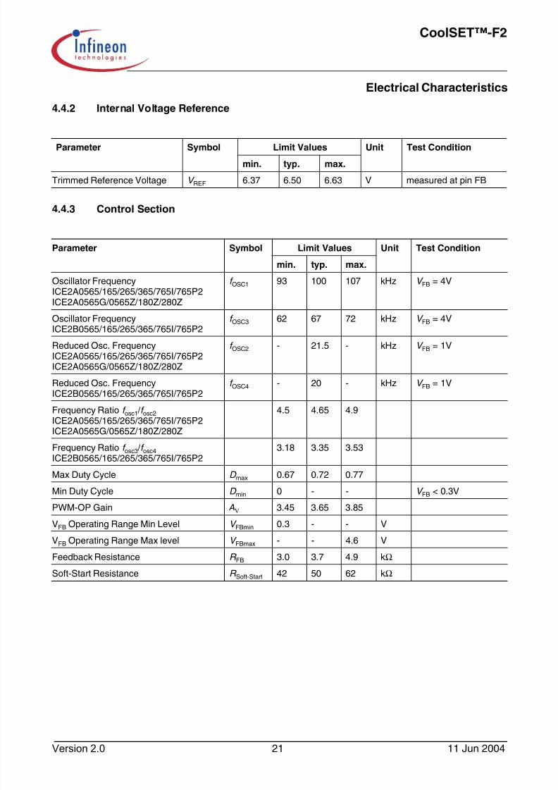
4.4.2 Internal Voltage Reference
4.4.3 Control Section
Parameter Symbol Limit Values Unit Test Condition
min. typ. max.
Trimmed Reference Voltage V REF 6.37 6.50 6.63 V measured at pin FB
Parameter Symbol Limit Values Unit Test Condition
min. typ. max.
Oscillator FrequencyICE2A0565/165/265/365/765I/765P2ICE2A0565G/0565Z/180Z/280Z
f OSC1 93 100 107 kHz V FB = 4V
Oscillator FrequencyICE2B0565/165/265/365/765I/765P2
f OSC3 62 67 72 kHz V FB = 4V
Reduced Osc. FrequencyICE2A0565/165/265/365/765I/765P2ICE2A0565G/0565Z/180Z/280Z
f OSC2 - 21.5 - kHz V FB = 1V
Reduced Osc. FrequencyICE2B0565/165/265/365/765I/765P2
f OSC4 - 20 - kHz V FB = 1V
Frequency Ratio f osc1
/ f osc2ICE2A0565/165/265/365/765I/765P2
ICE2A0565G/0565Z/180Z/280Z
4.5 4.65 4.9
Frequency Ratio f osc3 / f osc4
ICE2B0565/165/265/365/765I/765P23.18 3.35 3.53
Max Duty Cycle D max 0.67 0.72 0.77
Min Duty Cycle D min 0 - - V FB < 0.3V
PWM-OP Gain AV
3.45 3.65 3.85
VFB Operating Range Min Level V FBmin 0.3 - - V
VFB Operating Range Max level V FBmax - - 4.6 V
Feedback Resistance R FB 3.0 3.7 4.9 kΩ
Soft-Start Resistance R Soft-Start 42 50 62 kΩ
7/16/2019 datos datashet
http://slidepdf.com/reader/full/datos-datashet 22/36
CoolSET™-F2
Electrical Characteristics
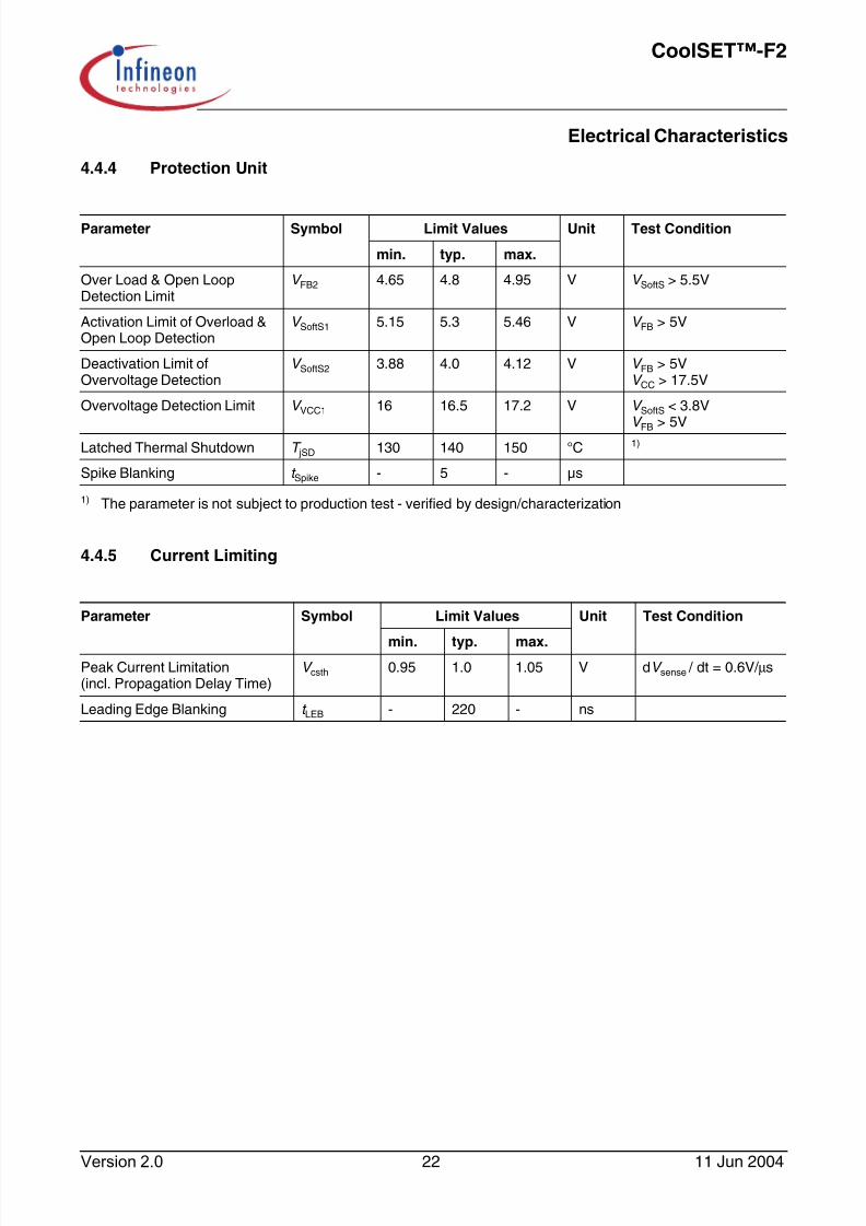
4.4.4 Protection Unit
4.4.5 Current Limiting
Parameter Symbol Limit Values Unit Test Condition
min. typ. max.
Over Load & Open LoopDetection Limit
V FB2 4.65 4.8 4.95 V V SoftS > 5.5V
Activation Limit of Overload &Open Loop Detection
V SoftS1 5.15 5.3 5.46 V V FB > 5V
Deactivation Limit ofOvervoltage Detection
V SoftS2 3.88 4.0 4.12 V V FB > 5VV CC > 17.5V
Overvoltage Detection Limit V VCC1 16 16.5 17.2 V V SoftS < 3.8V
V FB > 5VLatched Thermal Shutdown T jSD 130 140 150 °C 1)
1) The parameter is not subject to production test - verified by design/characterization
Spike Blanking t Spike - 5 - µs
Parameter Symbol Limit Values Unit Test Condition
min. typ. max.Peak Current Limitation(incl. Propagation Delay Time)
V csth 0.95 1.0 1.05 V dV sense / dt = 0.6V/ µs
Leading Edge Blanking t LEB - 220 - ns

7/16/2019 datos datashet
http://slidepdf.com/reader/full/datos-datashet 23/36
CoolSET™-F2
Electrical Characteristics
4.4.6 CoolMOS™ Section
Parameter Symbol Limit Values Unit Test Condition
min. typ. max.
Drain Source Breakdown VoltageICE2A0565/165/265/365/765I/765P2ICE2B0565/165/265/365/765I/765P2ICE2A0565G/0565Z
V (BR)DSS 600650
--
--
VV
T j=25°CT j=110°C
Drain Source Breakdown VoltageICE2A180Z/280Z
V (BR)DSS 800870
--
--
VV
T j=25°CT j=110°C
Drain SourceOn-Resistance
ICE2A0565 R DSon1 --
4.710.0
5.512.5
Ω
Ω
T j=25°CT j=125°C
ICE2A165 R DSon2 --
36.6
3.37.3
Ω
Ω
T j=25°CT j=125°C
ICE2A265 R DSon3 --
0.91.9
1.082.28
Ω
Ω
T j=25°CT j=125°C
ICE2A365 R DSon4 --
0.450.95
0.541.14
Ω
Ω
T j=25°CT j=125°C
ICE2B0565 R DSon5 --
4.710.0
5.512.5
Ω
Ω
T j=25°CT j=125°C
ICE2B165 R DSon6 --
36.6
3.37.3
Ω
Ω
T j=25°CT j=125°C
ICE2B265 R DSon7 --
0.91.9
1.082.28
ΩΩ
T j=25°CT j=125°C
ICE2B365 R DSon8 --
0.450.95
0.541.14
Ω
Ω
T j=25°CT j=125°C
ICE2A0565G R DSon9 --
4.710.0
5.512.5
Ω
Ω
T j=25°CT j=125°C
ICE2A0565Z R DSon10 --
4.710.0
5.512.5
Ω
Ω
T j=25°CT j=125°C
ICE2A180Z R DSon11 --
36.6
3.37.3
Ω
Ω
T j=25°CT j=125°C
ICE2A280Z R DSon12 --
0.81.7
1.062.04
ΩΩ
T j=25°CT j=125°C
ICE2A765I R DSon13 --
0.450.95
0.541.14
Ω
Ω
T j=25°CT j=125°C
ICE2B765I R DSon14 --
0.450.95
0.541.14
Ω
Ω
T j=25°CT j=125°C
ICE2A765P2 R DSon15 --
0.450.95
0.541.14
Ω
Ω
T j=25°CT j=125°C
ICE2B765P2 R DSon16 --
0.450.95
0.541.14
Ω
Ω
T j=25°CT j=125°C

7/16/2019 datos datashet
http://slidepdf.com/reader/full/datos-datashet 24/36
CoolSET™-F2
Electrical Characteristics
Parameter Symbol Limit Values Unit Test Condition
min. typ. max.
Effective outputcapacitance,energy related
ICE2A0565 C o(er)1 - 4.751 - pF V DS =0V to 480V
ICE2A165 C o(er)2 - 7 - pF
ICE2A265 C o(er)3 - 21 - pF
ICE2A365 C o(er)4 - 30 - pF
ICE2B0565 C o(er)5 - 4.751 - pF
ICE2B165 C o(er)6 - 7 - pF
ICE2B265 C o(er)7 - 21 - pF
ICE2B365 C o(er)8 - 30 - pF
ICE2A0565G C o(er)9 - 4.751 - pF
ICE2A0565Z C o(er)10 - 4.751 - pF
ICE2A180Z C o(er)11 - 7 - pF
ICE2A280Z C o(er)12 - 22 - pF
ICE2A765I C o(er)13 - 30 - pF
ICE2B765I C o(er)14 - 30 - pF
ICE2A765P2 C o(er)15 - 30 - pF
ICE2B765P2 C o(er)16
- 30 - pF
Zero Gate Voltage Drain Current I DSS - 0.5 - µA V VCC=0V
Rise Time t rise - 301)
1) Measured in a Typical Flyback Converter Application
- ns
Fall Time t fall - 301) - ns
7/16/2019 datos datashet
http://slidepdf.com/reader/full/datos-datashet 25/36
CoolSET™-F2
Typical Performance Characteristics
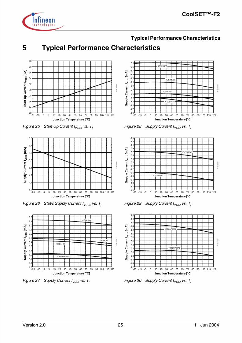
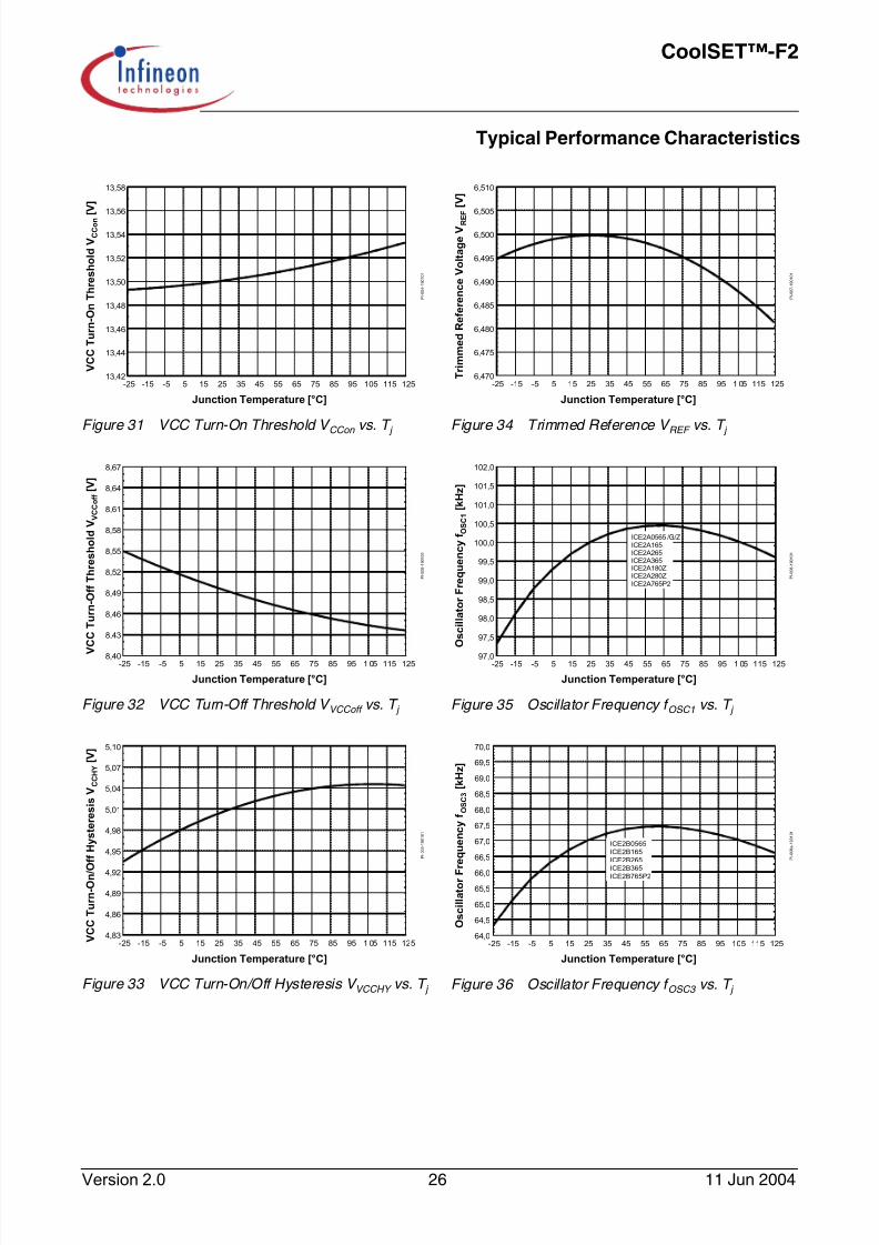
5 Typical Performance Characteristics
Figure 25 Start Up Current I VCC1 vs. T j
Figure 26 Static Supply Current I VCC2 vs. T j
Figure 27 Supply Current I VCCI vs. T j
Figure 28 Supply Current I VCCI vs. T j
Figure 29 Supply Current I VCCI vs. T j
Figure 30 Supply Current I VCCI vs. T j
Junction Temperature [°C]
S t a r t U p C u r r e n t I V
C C 1
[ µ A ]
P I - 0 0 1
- 1 9 0 1 0 1
22
24
26
28
30
32
34
36
38
40
-25 -15 -5 5 15 25 35 45 55 65 75 85 95 1 05 115 125
Junction Temperature [°C]
S u
p p l y C u r r e n t I V
C C 2
[ m A ]
P I - 0 0 3
- 1 9 0 1 0 1
4,5
4,7
4,9
5,1
5,3
5,5
5,7
5,9
-25 -15 -5 5 15 25 35 45 55 65 75 85 95 105 115 125
Junction Temperature [°C]
S u p p l y C u r r e n
t I V
C C i
[ m A ]
P I - 0 0 2
- 1 9 0 1 0 1
4,0
4,4
4,8
5,2
5,6
6,0
6,4
6,8
7,2
7,6
8,0
8,4
8,8
-25 -15 -5 5 15 25 35 45 55 65 75 85 95 105 115 125
ICE2A0565
ICE2A165
ICE2A265
ICE2A365
/G/Z
Junction Temperature [°C]
S u p p l y C u r r e n t I V
C C i
[ m A ]
P I - 0 0 2
- 1 9 0 1 0 1
4,5
4,7
4,9
5,1
5,3
5,5
5,7
5,9
6,1
6,3
6,5
6,7
6,9
7,1
-25 -15 -5 5 15 25 35 45 55 65 75 85 95 105 115 125
ICE2B165
ICE2B365
ICE2B265
ICE2B0565
Junction Temperature [°C]
S u
p p l y C u r r e n t I V
C C i
[ m A ]
P I - 0 0 2
- 1 9 0 1 0 1
5,5
5,7
5,96,1
6,3
6,5
6,7
6,9
7,1
7,3
7,5
7,7
7,9
8,1
8,3
8,5
-25 -15 -5 5 15 25 35 45 55 65 75 85 95 1 05 115 125
ICE2A280Z
ICE2A180Z
Junction Temperature [°C]
S u p p l y C u r r e n
t I V
C C i
[ m A ]
P I - 0 0 2
- 1 9 0 1 0 1
6,2
6,4
6,6
6,8
7,0
7,2
7,4
7,6
7,8
8,0
8,2
8,4
8,6
8,8
9,0
-25 -15 -5 5 15 25 35 45 55 65 75 85 95 1 05 115 125
ICE2A765P2
ICE2B765P2
7/16/2019 datos datashet
http://slidepdf.com/reader/full/datos-datashet 26/36
CoolSET™-F2
Typical Performance Characteristics
Figure 31 VCC Turn-On Threshold V CCon vs. T j
Figure 32 VCC Turn-Off Threshold V VCCoff vs. T j
Figure 33 VCC Turn-On/Off Hysteresis V VCCHY vs. T j
Figure 34 Trimmed Reference V REF vs. T j
Figure 35 Oscillator Frequency f OSC1 vs. T j
Figure 36 Oscillator Frequency f OSC3 vs. T j
Junction Temperature [°C]
V C C T u r n - O n T h r e s h o l d V
C C o n
[ V ]
P I - 0 0 4
- 1 9 0 1 0 1
13,42
13,44
13,46
13,48
13,50
13,52
13,54
13,56
13,58
-25 -15 -5 5 15 25 35 45 55 65 75 85 95 105 115 125
Junction Temperature [°C]
V C C T u r n - O f f T h r e s h o l d V
V C C o f f
[ V ]
P I - 0 0 5
- 1 9 0 1 0 1
8,40
8,43
8,46
8,49
8,52
8,55
8,58
8,61
8,64
8,67
-25 -15 -5 5 15 25 35 45 55 65 75 85 95 1 05 115 125
Junction Temperature [°C]
V C C T u r n - O n / O f f H y s t e r e s i s V
C C H Y
[ V ]
P I - 0 0 6
- 1 9 0 1 0 1
4,83
4,86
4,89
4,92
4,95
4,98
5,01
5,04
5,07
5,10
-25 -15 -5 5 15 25 35 45 55 65 75 85 95 1 05 115 125
Junction Temperature [°C]
T r i m m e d R e f e r e n c e V o l t a g e V
R E
F [ V ]
P I - 0 0 7
- 1 9 0 1 0 1
6,470
6,475
6,480
6,485
6,490
6,495
6,500
6,505
6,510
-25 -15 -5 5 15 25 35 45 55 65 75 85 95 1 05 115 125
Junction Temperature [°C]
O s c i l l a t o r F r e q u e n c y f O
S C 1
[ k H z ]
P I - 0 0 8
- 1 9 0 1 0 1
97,0
97,5
98,0
98,5
99,0
99,5
100,0
100,5
101,0
101,5
102,0
-25 -15 -5 5 15 25 35 45 55 65 75 85 95 1 05 115 125
ICE2A0565ICE2A165ICE2A265ICE2A365ICE2A180ZICE2A280ZICE2A765P2
/G/Z
Junction Temperature [°C]
O s c i l l a t o r F
r e q u e n c y f O
S C 3
[ k H z ]
P I - 0 0 8
a -
1 9 0 1 0 1
64,0
64,5
65,0
65,5
66,0
66,5
67,0
67,5
68,0
68,5
69,0
69,5
70,0
-25 -15 -5 5 15 25 35 45 55 65 75 85 95 105 115 125
ICE2B0565
ICE2B165
ICE2B265
ICE2B365
ICE2B765P2
7/16/2019 datos datashet
http://slidepdf.com/reader/full/datos-datashet 27/36
CoolSET™-F2
Typical Performance Characteristics
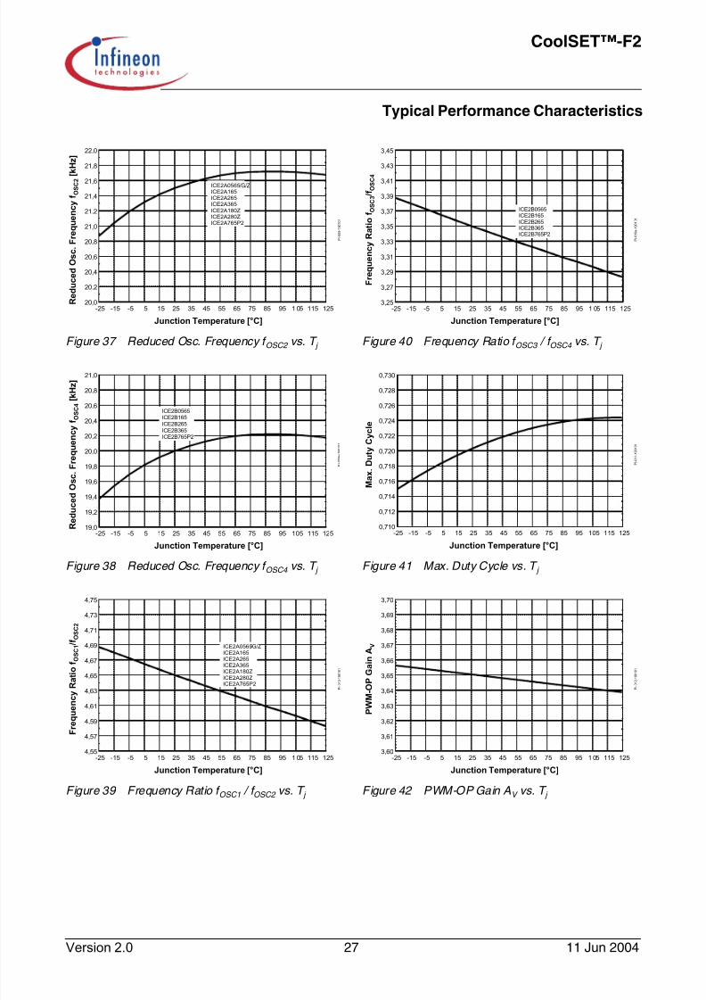
Figure 37 Reduced Osc. Frequency f OSC2 vs. T j
Figure 38 Reduced Osc. Frequency f OSC4 vs. T j
Figure 39 Frequency Ratio f OSC1 / f OSC2 vs. T j
Figure 40 Frequency Ratio f OSC3 / f OSC4 vs. T j
Figure 41 Max. Duty Cycle vs. T j
Figure 42 PWM-OP Gain AV vs. T j
Junction Temperature [°C]
R e d u c e d O s c .
F r e q u e n c y f O
S C 2 [
k H z ]
P I - 0 0 9
- 1 9 0 1 0 1
20,0
20,2
20,4
20,6
20,8
21,0
21,2
21,4
21,6
21,8
22,0
-25 -15 -5 5 15 25 35 45 55 65 75 85 95 1 05 115 125
ICE2A0565ICE2A165ICE2A265ICE2A365ICE2A180ZICE2A280ZICE2A765P2
/G/Z
Junction Temperature [°C]
R
e d u c e d O s c .
F r e q u e n c y f O
S C 4
[ k H z ]
P I - 0 0 9
a - 1
9 0 1 0 1
19,0
19,2
19,4
19,6
19,8
20,0
20,2
20,4
20,6
20,8
21,0
-25 -15 -5 5 15 25 35 45 55 65 75 85 95 105 115 125
ICE2B0565ICE2B165
ICE2B265
ICE2B365ICE2B765P2
Junction Temperature [°C]
F r e q u e n c y R a t i o f O
S C 1
/ f O S C 2
P I - 0 1 0
- 1 9 0 1 0 1
4,55
4,57
4,59
4,61
4,63
4,65
4,67
4,69
4,71
4,73
4,75
-25 -15 -5 5 15 25 35 45 55 65 75 85 95 1 05 115 125
ICE2A0565ICE2A165ICE2A265ICE2A365ICE2A180ZICE2A280ZICE2A765P2
/G/Z
Junction Temperature [°C]
F r e q u e n c y R a t i o f O
S C 3
/ f O S C 4
P I - 0 1 0
a - 1
9 0 1 0 1
3,25
3,27
3,29
3,31
3,33
3,35
3,37
3,39
3,41
3,43
3,45
-25 -15 -5 5 15 25 35 45 55 65 75 85 95 1 05 115 125
ICE2B0565ICE2B165ICE2B265ICE2B365ICE2B765P2
Junction Temperature [°C]
M a x .
D u t y C y c l e
P I - 0 1 1
- 1 9 0 1 0 1
0,710
0,712
0,714
0,716
0,718
0,720
0,722
0,724
0,726
0,728
0,730
-25 -15 -5 5 15 25 35 45 55 65 75 85 95 105 115 125
Junction Temperature [°C]
P W M - O P G a i n A
V
P I - 0 1 2
- 1 9 0 1 0 1
3,60
3,61
3,62
3,63
3,64
3,65
3,66
3,67
3,68
3,69
3,70
-25 -15 -5 5 15 25 35 45 55 65 75 85 95 1 05 115 125

7/16/2019 datos datashet
http://slidepdf.com/reader/full/datos-datashet 28/36
CoolSET™-F2
Typical Performance Characteristics
Figure 43 Feedback Resistance R FB vs. T j
Figure 44 Soft-Start Resistance R Soft-Start vs. T j
Figure 45 Detection Limit V FB2 vs. T j
Figure 46 Detection Limit V Soft-Start1 vs. T j
Figure 47 Detection Limit V Soft-Start2 vs. T j
Figure 48 Overvoltage Detection Limit V VCC1 vs. T j
Junction Temperature [°C]
F e e d b a c k R e s i s t a n c e R
F B
[ k O h
m ]
P I - 0 1 3
- 1 9 0 1 0 1
3,50
3,55
3,60
3,65
3,70
3,75
3,80
3,85
3,90
3,95
4,00
-25 -15 -5 5 15 25 35 45 55 65 75 85 95 1 05 115 125
Junction Temperature [°C]
S o
f t - S t a r t R e s i s t a n c e R
S o f t - S t a r t
[ k O h m ]
P I - 0 1 4
- 1 9 0 1 0 1
40
42
44
46
48
50
52
54
56
58
-25 -15 -5 5 15 25 35 45 55 65 75 85 95 1 05 115 125
Junction Temperature [°C]
D e t e c t i o n L i m i t V
F B 2
[ V ]
P I - 0 1 5
- 1 9 0 1 0 1
4,780
4,785
4,790
4,795
4,800
4,805
4,810
-25 -15 -5 5 15 25 35 45 55 65 75 85 95 1 05 115 125
Junction Temperature [°C]
D e t e c t i o n L i m i t V
S o f t - S t a r t 1
[ V ]
P I - 0 1 6
- 1 9 0 1 0 1
5,270
5,275
5,280
5,285
5,290
5,295
5,300
5,305
5,310
5,315
5,320
-25 -15 -5 5 15 25 35 45 55 65 75 85 95 1 05 115 125
Junction Temperature [°C]
D e t e c t i o n L i m i t V
S o f t - S t a r t 2
[ V ]
P I - 0 1 7
- 1 9 0 1 0 1
3,95
3,96
3,97
3,98
3,99
4,00
4,01
4,02
4,03
4,04
4,05
-25 -15 -5 5 15 25 35 45 55 65 75 85 95 1 05 115 125
Junction Temperature [°C]
O v e r v o l t a g e D
e t e c t i o n L i m i t V
V C C 1
[ V ]
P I - 0 1 8
- 1 9 0 1 0 1
16,20
16,25
16,30
16,35
16,40
16,45
16,50
16,55
16,60
16,65
16,70
16,75
16,80
-25 -15 -5 5 15 25 35 45 55 65 75 85 95 1 05 115 125
7/16/2019 datos datashet
http://slidepdf.com/reader/full/datos-datashet 29/36
CoolSET™-F2
Typical Performance Characteristics
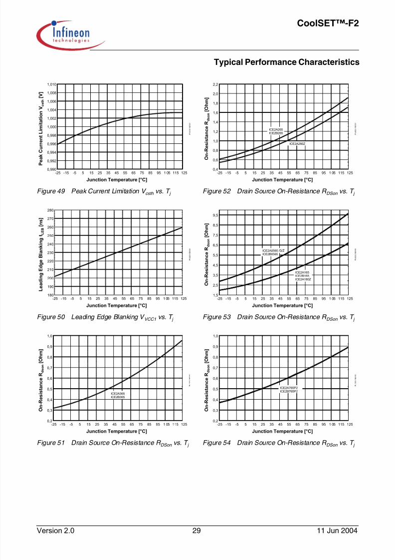
Figure 49 Peak Current Limitation V csth vs. T j
Figure 50 Leading Edge Blanking V VCC1 vs. T j
Figure 51 Drain Source On-Resistance R DSon vs. T j
Figure 52 Drain Source On-Resistance R DSon vs. T j
Figure 53 Drain Source On-Resistance R DSon vs. T j
Figure 54 Drain Source On-Resistance R DSon vs. T j
Junction Temperature [°C]
P e a k C u r r e n t L i m i t a t i o n V
c s t h [
V ]
P I - 0 1 9
- 1 9 0 1 0 1
0,990
0,992
0,994
0,996
0,998
1,000
1,002
1,004
1,006
1,008
1,010
-25 -15 -5 5 15 25 35 45 55 65 75 85 95 1 05 115 125
Junction Temperature [°C]
L e a d i n g E d g e B l a n k i n g t L
E B
[ n s ]
P I - 0 2 0
- 1 9 0 1 0 1
180
190
200
210
220
230
240
250
260
270
280
-25 -15 -5 5 15 25 35 45 55 65 75 85 95 1 05 115 125
Junction Temperature [°C]
O n - R e s i s
t a n c e R
d s o n
[ O h m ]
P I - 0 2 2
- 1 9 0 1 0 1
0,2
0,3
0,4
0,5
0,6
0,7
0,8
0,9
1,0
-25 -15 -5 5 15 25 35 45 55 65 75 85 95 1 05 115 125
ICE2A365ICE2B365
Junction Temperature [°C]
O n - R e s i s t a n c e R
d s o n
[ O h m ]
P I - 0 2 2
- 1 9 0 1 0 1
0,4
0,6
0,8
1,0
1,2
1,4
1,6
1,8
2,0
2,2
-25 -15 -5 5 15 25 35 45 55 65 75 85 95 1 05 115 125
ICE2A280Z
ICE2A265ICE2B265
Junction Temperature [°C]
O n - R e s i s t a n c e R
d s o n
[ O h m ]
P I - 0 2 2
- 1 9 0 1 0 1
1,5
2,5
3,5
4,5
5,5
6,5
7,5
8,5
9,5
-25 -15 -5 5 15 25 35 45 55 65 75 85 95 1 05 115 125
ICE2A0565ICE2B0565
ICE2A165ICE2B165ICE2A180Z
/G/Z
Junction Temperature [°C]
O n - R e s i s
t a n c e R
d s o n
[ O h m ]
P I - 0 2 2
- 1 9 0 1 0 1
0,2
0,3
0,4
0,5
0,6
0,7
0,8
0,9
1,0
-25 -15 -5 5 15 25 35 45 55 65 75 85 95 1 05 115 125
ICE2A765P2
ICE2B765P2

7/16/2019 datos datashet
http://slidepdf.com/reader/full/datos-datashet 30/36
CoolSET™-F2
Typical Performance Characteristics
Figure 55 Breakdown Voltage V BR(DSS) vs. T j
Figure 56 Breakdown Voltage V BR(DSS) vs. T j
Junction Temperature [°C]
B r e a k d o w n V o l t a g e V
( B R ) D S S [
V ]
P I - 0 2 5
- 1 9 0 1 0 1
560
580
600
620
640
660
680
700
720
-25 -15 -5 5 15 25 35 45 55 65 75 85 95 1 05 115 125
ICE2A0565ICE2A165
ICE2A265
ICE2A365
ICE2B0565ICE2B165
ICE2B265
ICE2B365ICE2A765P2
ICE2B765P2
/G/Z
Junction Temperature [°C]
B r e a k d o w n V o l t a g e V
( B R ) D S S
[ V ]
P I - 0 2 5
- 1 9 0 1 0 1
780
800
820
840
860
880
900
920
940
-25 -15 -5 5 15 25 35 45 55 65 75 85 95 1 05 115 125
ICE2A180ZICE2A280Z

7/16/2019 datos datashet
http://slidepdf.com/reader/full/datos-datashet 31/36
CoolSET™-F2
Layout Recommendation for C18
6 Layout Recommendation for C18
Note: Only for ICE2A765I/P2 and ICE2B765I/P2
Figure 57 Layout Recommendation for ICE2A765I/P2 and ICE2B765I/P2
Soft Start Capacitor Layout Recommendation in Detail
Figure 57 A Layout of Board EVALSF2_ICE2B765P2
To improve the startup behavior of the IC during
startup or auto restart mode, place the soft start
capacitor C18 (red section Detail X in Figure 57 A)
as close as possible to the soft start PIN 6 and
GND PIN 4. More details see Detail X in Figure
57B.
Figure 57B Detail X, Soft Start Capacitor C18 Layout
Recommendation
Place Soft Start capacitor C18 in the same way as
shown in Detail X (blue mark).
Detail X

7/16/2019 datos datashet
http://slidepdf.com/reader/full/datos-datashet 32/36
CoolSET™-F2
Outline Dimension
7 Outline Dimension
Figure 58 P-DIP-8-6 (Plastic Dual In-line Package)
Figure 59 P-DIP-7-1 (Plastic Dual In-line Package)
Dimensions in mm
P-DIP-8-6
(Plastic Dual In-line
Package)
P-DIP-7-1
(Plastic Dual In-line
Package)
Does not include plastic or metal protrusion of 0.25 max. per side
9.52
Index Marking
±0.25
0.35
2.54
0.46
1
7
±0.1
1.7 MAX.
41)
7x
5
3 . 2 5 M I N .
4 . 3 7 M A X .
0 . 3 8 M I N .
±0.25
8.9 ±1
0.25
6.35
+0.1
±0.387.87
1)
1)

7/16/2019 datos datashet
http://slidepdf.com/reader/full/datos-datashet 33/36

7/16/2019 datos datashet
http://slidepdf.com/reader/full/datos-datashet 34/36
CoolSET™-F2
Outline Dimension
Figure 62 P-DSO-16/12 (Plastic Dual Small Outline Package)
Dimensions in mm
P-DSO-16/12
(Plastic Dual Small Outline Package)

7/16/2019 datos datashet
http://slidepdf.com/reader/full/datos-datashet 35/36
Qualität hat für uns eine umfassendeBedeutung. Wir wollen allen IhrenAnsprüchen in der bestmöglichenWeise gerecht werden. Es geht uns alsonicht nur um die Produktqualität –unsere Anstrengungen geltengleichermaßen der Lieferqualität undLogistik, dem Service und Support
sowie allen sonstigen Beratungs- undBetreuungsleistungen.
Dazu gehört eine bestimmteGeisteshaltung unserer Mitarbeiter.Total Quality im Denken und Handelngegenüber Kollegen, Lieferanten undIhnen, unserem Kunden. UnsereLeitlinie ist jede Aufgabe mit „NullFehlern“ zu lösen – in offenerSichtweise auch über den eigenenArbeitsplatz hinaus – und uns ständig
zu verbessern.Unternehmensweit orientieren wir unsdabei auch an „top“ (Time OptimizedProcesses), um Ihnen durch größereSchnelligkeit den entscheidendenWettbewerbsvorsprung zu verschaffen.
Geben Sie uns die Chance, hoheLeistung durch umfassende Qualität zubeweisen.
Wir werden Sie überzeugen.
Quality takes on an allencompassingsignificance at Semiconductor Group.For us it means living up to each andevery one of your demands in the bestpossible way. So we are not onlyconcerned with product quality. Wedirect our efforts equally at quality ofsupply and logistics, service and
support, as well as all the other ways inwhich we advise and attend to you.
Part of this is the very special attitude ofour staff. Total Quality in thought anddeed, towards co-workers, suppliersand you, our customer. Our guideline is“do everything with zero defects”, in anopen manner that is demonstratedbeyond your immediate workplace, andto constantly improve.
Throughout the corporation we also
think in terms of Time OptimizedProcesses (top), greater speed on ourpart to give you that decisivecompetitive edge.
Give us the chance to prove the best ofperformance through the best of quality– you will be convinced.
h t t p : / / w w w . i n f i n e o n . c o m
Total Quality Management

7/16/2019 datos datashet
http://slidepdf.com/reader/full/datos-datashet 36/36
This datasheet has been download from:
www.datasheetcatalog.com
Datasheets for electronics components.