datasheet - stm32mp157c - arm® dual cortex®-a7 650 mhz ... · this is information on a product in...
TRANSCRIPT

This is information on a product in full production.
February 2019 DS12505 Rev 1 1/251
STM32MP157C
Arm® dual Cortex®-A7 650 MHz + Cortex®-M4 MPU, 3D GPU, TFT/DSI, 37 comm. interfaces, 29 timers, adv. analog, crypto
Datasheet - production data
Features
Core
• 32-bit dual-core Arm® Cortex®-A7
– L1 32-Kbyte I / 32-Kbyte D for each core
– 256-Kbyte unified level 2 cache
– Arm® NEON™ and Arm® TrustZone®
• 32-bit Arm® Cortex®-M4 with FPU/MPU
– Up to 209 MHz (Up to 703 CoreMark®)
Memories
• External DDR memory up to 1 Gbyte
– up to LPDDR2/LPDDR3-1066 16/32-bit
– up to DDR3/DDR3L-1066 16/32-bit
• 708 Kbytes of internal SRAM: 256 KB of AXI SYSRAM + 384 KB of AHB SRAM + 64 KB of AHB SRAM in backup domain and 4 KB of SRAM in backup domain
• Dual mode Quad-SPI memory interface
• Flexible external memory controller with up to 16-bit data bus: parallel interface to connect external ICs and SLC NAND memories with up to 8-bit ECC
Security/safety
• Secure boot, TrustZone® peripherals, active tamper
• Cortex®-M4 resources isolation
Reset and power management
• 1.71 V to 3.6 V I/Os supply (5 V-tolerant I/Os)
• POR, PDR, PVD and BOR
• On-chip LDOs (RETRAM, BKPSRAM, DSI 1.2 V, USB 1.8 V, 1.1 V)
• Backup regulator (~0.9 V)
• Internal temperature sensors
• Low-power modes: Sleep, Stop and Standby
• LPDDR2/3 retention in Standby mode
• Controls for PMIC companion chip
Low-power consumption
• Total current consumption down to 6 µA
Clock management
• Internal oscillators: 64 MHz HSI oscillator, 4 MHz CSI oscillator, 32 kHz LSI oscillator
• External oscillators: 8-48 MHz HSE oscillator, 32.768 kHz LSE oscillator
• 6 × PLLs with fractional mode
General-purpose input/outputs
• Up to 176 I/O ports with interrupt capability
– Up to 8 secure I/Os
– Up to 6 Wakeup, 3 Tamper, 1 Active-Tamper
Interconnect matrix
• 2 bus matrices
– 64-bit Arm® AMBA® AXI interconnect, up to 266 MHz
– 32-bit Arm® AMBA® AHB interconnect, up to 209 MHz
3 DMA controllers to unload the CPU
• 48 physical channels in total
• 1 × high-speed general-purpose master direct memory access controller (MDMA)
• 2 × dual-port DMAs with FIFO and request router capabilities for optimal peripheral management
LFBGA
TFBGA361 (12 × 12 mm)TFBGA257 (10 × 10 mm)
min Pitch 0.5mm
TFBGA
LFBGA448 (18 × 18mm)LFBGA354 (16 × 16mm)
Pitch 0.8mm
www.st.com

STM32MP157C
2/251 DS12505 Rev 1
Up to 37 communication peripherals
• 6 × I2C FM+ (1 Mbit/s, SMBus/PMBus)
• 4 × UART + 4 × USART (12.5 Mbit/s, ISO7816 interface, LIN, IrDA, SPI slave)
• 6 × SPI (50 Mbit/s, including 3 with full duplex I2S audio class accuracy via internal audio PLL or external clock)
• 4 × SAI (stereo audio: I2S, PDM, SPDIF Tx)
• SPDIF Rx with 4 inputs
• HDMI-CEC interface
• MDIO Slave interface
• 3 × SDMMC up to 8-bit (SD / e•MMC™ / SDIO)
• 2 × CAN controllers supporting CAN FD protocol, out of which one supports time-triggered CAN (TTCAN)
• 2 × USB 2.0 high-speed Host + 1 × USB 2.0 full-speed OTG simultaneously
– or 1 × USB 2.0 high-speed Host + 1 × USB 2.0 high-speed OTG simultaneously
• 10/100M or Gigabit Ethernet GMAC
– IEEE 1588v2 hardware, MII/RMII/GMII/RGMII
• 8- to 14-bit camera interface up to 140 Mbyte/s
6 analog peripherals
• 2 × ADCs with 16-bit max. resolution (12 bits 5 Msps, 14 bits 4.4 Msps, 16 bits 250 ksps)
• 1 × temperature sensor
• 2 × 12-bit D/A converters (1 MHz)
• 1 × digital filters for sigma delta modulator (DFSDM) with 8 channels/6 filters
• Internal or external ADC/DAC reference VREF+
Graphics
• 3D GPU: Vivante® - OpenGL® ES 2.0
– Up to 26 Mtriangle/s, 133 Mpixel/s
• LCD-TFT controller, up to 24-bit // RGB888
– up to WXGA (1366 × 768) @60 fps
– Two layers with programmable colour LUT
• MIPI® DSI 2 data lanes up to 1 GHz each
Up to 29 timers and 3 watchdogs
• 2 × 32-bit timers with up to 4 IC/OC/PWM or pulse counter and quadrature (incremental) encoder input
• 2 × 16-bit advanced motor control timers
• 10 × 16-bit general-purpose timers (including 2 basic timers without PWM)
• 5 × 16-bit low-power timers
• RTC with sub-second accuracy and hardware calendar
• 2 × 4 Cortex®-A7 system timers (secure, non-secure, virtual, hypervisor)
• 1 × SysTick M4 timer
• 3 × watchdogs (2 × independent and window)
Hardware acceleration
• AES 128, 192, 256, TDES
• HASH (MD5, SHA-1, SHA224, SHA256), HMAC
• 2 × true random number generator (3 oscillators each)
• 2 × CRC calculation unit
Debug mode
• Arm® CoreSight™ trace and debug: SWD and JTAG interfaces
• 8-Kbyte embedded trace buffer
3072-bit fuses including 96-bit unique ID, up to 1184-bit available for user
All packages are ECOPACK®2 compliant

DS12505 Rev 1 3/251
STM32MP157C Contents
7
Contents
1 Introduction . . . . . . . . . . . . . . . . . . . . . . . . . . . . . . . . . . . . . . . . . . . . . . . 13
2 Description . . . . . . . . . . . . . . . . . . . . . . . . . . . . . . . . . . . . . . . . . . . . . . . . 14
3 Functional overview . . . . . . . . . . . . . . . . . . . . . . . . . . . . . . . . . . . . . . . . 20
3.1 Dual-core Arm® Cortex®-A7 subsystem . . . . . . . . . . . . . . . . . . . . . . . . . . 20
3.1.1 Features . . . . . . . . . . . . . . . . . . . . . . . . . . . . . . . . . . . . . . . . . . . . . . . . . 20
3.1.2 Overview . . . . . . . . . . . . . . . . . . . . . . . . . . . . . . . . . . . . . . . . . . . . . . . . 20
3.2 Arm® Cortex®-M4 with FPU . . . . . . . . . . . . . . . . . . . . . . . . . . . . . . . . . . . 22
3.3 Graphic processing unit (GPU) . . . . . . . . . . . . . . . . . . . . . . . . . . . . . . . . 22
3.4 Memories . . . . . . . . . . . . . . . . . . . . . . . . . . . . . . . . . . . . . . . . . . . . . . . . . 24
3.4.1 External SDRAM . . . . . . . . . . . . . . . . . . . . . . . . . . . . . . . . . . . . . . . . . . 24
3.4.2 Embedded SRAM . . . . . . . . . . . . . . . . . . . . . . . . . . . . . . . . . . . . . . . . . 24
3.5 DDR3/DDR3L/LPDDR2/LPDDR3 controller (DDRCTRL) . . . . . . . . . . . . 25
3.6 TrustZone address space controller for DDR (TZC) . . . . . . . . . . . . . . . . 26
3.7 Boot modes . . . . . . . . . . . . . . . . . . . . . . . . . . . . . . . . . . . . . . . . . . . . . . . 27
3.8 Power supply management . . . . . . . . . . . . . . . . . . . . . . . . . . . . . . . . . . . 28
3.8.1 Power supply scheme . . . . . . . . . . . . . . . . . . . . . . . . . . . . . . . . . . . . . . 28
3.8.2 Power supply supervisor . . . . . . . . . . . . . . . . . . . . . . . . . . . . . . . . . . . . 30
3.9 Low-power strategy . . . . . . . . . . . . . . . . . . . . . . . . . . . . . . . . . . . . . . . . . 31
3.10 Reset and clock controller (RCC) . . . . . . . . . . . . . . . . . . . . . . . . . . . . . . . 32
3.10.1 Clock management . . . . . . . . . . . . . . . . . . . . . . . . . . . . . . . . . . . . . . . . 32
3.10.2 System reset sources . . . . . . . . . . . . . . . . . . . . . . . . . . . . . . . . . . . . . . 33
3.11 Hardware semaphore (HSEM) . . . . . . . . . . . . . . . . . . . . . . . . . . . . . . . . . 33
3.12 Inter-processor communication controller (IPCC) . . . . . . . . . . . . . . . . . . 33
3.12.1 IPCC main features . . . . . . . . . . . . . . . . . . . . . . . . . . . . . . . . . . . . . . . . 34
3.13 General-purpose input/outputs (GPIOs) . . . . . . . . . . . . . . . . . . . . . . . . . . 34
3.14 TrustZone protection controller (ETZPC) . . . . . . . . . . . . . . . . . . . . . . . . . 34
3.15 Bus-interconnect matrix . . . . . . . . . . . . . . . . . . . . . . . . . . . . . . . . . . . . . . 35
3.16 DMA controllers . . . . . . . . . . . . . . . . . . . . . . . . . . . . . . . . . . . . . . . . . . . . 37
3.17 Nested vectored interrupt controller (NVIC) . . . . . . . . . . . . . . . . . . . . . . . 37
3.18 Extended interrupt and event controller (EXTI) . . . . . . . . . . . . . . . . . . . . 37

Contents STM32MP157C
4/251 DS12505 Rev 1
3.19 Cyclic redundancy check calculation unit (CRC1, CRC2) . . . . . . . . . . . . 38
3.20 Flexible memory controller (FMC) . . . . . . . . . . . . . . . . . . . . . . . . . . . . . . 38
3.21 Dual Quad-SPI memory interface (QUADSPI) . . . . . . . . . . . . . . . . . . . . . 38
3.22 Analog-to-digital converters (ADCs) . . . . . . . . . . . . . . . . . . . . . . . . . . . . . 39
3.23 Temperature sensor . . . . . . . . . . . . . . . . . . . . . . . . . . . . . . . . . . . . . . . . . 39
3.24 Digital temperature sensor (DTS) . . . . . . . . . . . . . . . . . . . . . . . . . . . . . . . 39
3.25 VBAT operation . . . . . . . . . . . . . . . . . . . . . . . . . . . . . . . . . . . . . . . . . . . . . 39
3.26 Digital-to-analog converters (DAC1, DAC2) . . . . . . . . . . . . . . . . . . . . . . . 40
3.27 Voltage reference buffer (VREFBUF) . . . . . . . . . . . . . . . . . . . . . . . . . . . . 41
3.28 Digital filter for sigma delta modulators (DFSDM1) . . . . . . . . . . . . . . . . . 41
3.29 Digital camera interface (DCMI) . . . . . . . . . . . . . . . . . . . . . . . . . . . . . . . . 43
3.30 LCD-TFT display controller (LTDC) . . . . . . . . . . . . . . . . . . . . . . . . . . . . . 43
3.31 Display serial interface (DSI) . . . . . . . . . . . . . . . . . . . . . . . . . . . . . . . . . . 44
3.32 True random number generator (RNG1, RNG2) . . . . . . . . . . . . . . . . . . . 44
3.33 Cryptographic and hash processors (CRYP1, CRYP2 and HASH1, HASH2) . . . . . . . . . . . . . . . . . . . . . . . . . . . . . . . . . . . . . . . . . . . 45
3.34 Boot and security and OTP control (BSEC) . . . . . . . . . . . . . . . . . . . . . . . 45
3.35 Timers and watchdogs . . . . . . . . . . . . . . . . . . . . . . . . . . . . . . . . . . . . . . . 45
3.35.1 Advanced-control timers (TIM1, TIM8) . . . . . . . . . . . . . . . . . . . . . . . . . 47
3.35.2 General-purpose timers (TIM2, TIM3, TIM4, TIM5, TIM12, TIM13, TIM14, TIM15, TIM16, TIM17) . . . . . . . . . . . . . . . . . . . . . . . . . . . . . . . . . . . . . . 47
3.35.3 Basic timers TIM6 and TIM7 . . . . . . . . . . . . . . . . . . . . . . . . . . . . . . . . . 48
3.35.4 Low-power timer (LPTIM1, LPTIM2, LPTIM3, LPTIM4, LPTIM5) . . . . . 48
3.35.5 Independent watchdog (IWDG1, IWDG2) . . . . . . . . . . . . . . . . . . . . . . . 48
3.35.6 System window watchdog (WWDG1) . . . . . . . . . . . . . . . . . . . . . . . . . . 48
3.35.7 SysTick timer (Cortex-M4) . . . . . . . . . . . . . . . . . . . . . . . . . . . . . . . . . . . 48
3.35.8 Generic timers (Cortex-A7 CNT) . . . . . . . . . . . . . . . . . . . . . . . . . . . . . . 49
3.36 System timer generation (STGEN) . . . . . . . . . . . . . . . . . . . . . . . . . . . . . . 49
3.37 Real-time clock (RTC) . . . . . . . . . . . . . . . . . . . . . . . . . . . . . . . . . . . . . . . 49
3.38 Tamper and backup registers (TAMP) . . . . . . . . . . . . . . . . . . . . . . . . . . . 50
3.39 Inter-integrated circuit interface (I2C1, I2C2, I2C3, I2C4, I2C5, I2C6) . . . 52
3.40 Universal synchronous asynchronous receiver transmitter (USART1, USART2, USART3, USART6 and UART4, UART5, UART7, UART8) . . . . . . . . . . . . . . . . . . . . . . . . . . . . . . . . . . . . . . . . . . . . 52
3.41 Serial peripheral interface (SPI1, SPI2, SPI3, SPI4, SPI5, SPI6)– inter- integrated sound interfaces (I2S1, I2S2, I2S3) . . . . . . . . . . 53

DS12505 Rev 1 5/251
STM32MP157C Contents
7
3.42 Serial audio interfaces (SAI1, SAI2, SAI3, SAI4) . . . . . . . . . . . . . . . . . . . 54
3.43 SPDIF receiver interface (SPDIFRX) . . . . . . . . . . . . . . . . . . . . . . . . . . . . 54
3.44 Management data input/output (MDIOS) . . . . . . . . . . . . . . . . . . . . . . . . . 55
3.45 Secure digital input/output MultiMediaCard interface (SDMMC1, SDMMC2, SDMMC3) . . . . . . . . . . . . . . . . . . . . . . . . . . . . . . 55
3.46 Controller area network (FDCAN1, FDCAN2) . . . . . . . . . . . . . . . . . . . . . 55
3.47 Universal serial bus high-speed host (USBH) . . . . . . . . . . . . . . . . . . . . . 56
3.48 USB on-the-go high-speed (OTG) . . . . . . . . . . . . . . . . . . . . . . . . . . . . . . 56
3.49 Gigabit Ethernet MAC interface (ETH1) . . . . . . . . . . . . . . . . . . . . . . . . . . 57
3.50 High-definition multimedia interface (HDMI) – Consumer electronics control (CEC) . . . . . . . . . . . . . . . . . . . . . . . . . . . . . . . . . . . . . 58
3.51 Debug infrastructure . . . . . . . . . . . . . . . . . . . . . . . . . . . . . . . . . . . . . . . . . 58
4 Pinouts, pin description and alternate functions . . . . . . . . . . . . . . . . . 59
5 Memory mapping . . . . . . . . . . . . . . . . . . . . . . . . . . . . . . . . . . . . . . . . . . 123
6 Electrical characteristics . . . . . . . . . . . . . . . . . . . . . . . . . . . . . . . . . . . 124
6.1 Parameter conditions . . . . . . . . . . . . . . . . . . . . . . . . . . . . . . . . . . . . . . . 124
6.1.1 Minimum and maximum values . . . . . . . . . . . . . . . . . . . . . . . . . . . . . . 124
6.1.2 Typical values . . . . . . . . . . . . . . . . . . . . . . . . . . . . . . . . . . . . . . . . . . . 124
6.1.3 Typical curves . . . . . . . . . . . . . . . . . . . . . . . . . . . . . . . . . . . . . . . . . . . 124
6.1.4 Loading capacitor . . . . . . . . . . . . . . . . . . . . . . . . . . . . . . . . . . . . . . . . 124
6.1.5 Pin input voltage . . . . . . . . . . . . . . . . . . . . . . . . . . . . . . . . . . . . . . . . . 124
6.1.6 Power supply scheme . . . . . . . . . . . . . . . . . . . . . . . . . . . . . . . . . . . . . 125
6.1.7 Current consumption measurement . . . . . . . . . . . . . . . . . . . . . . . . . . 126
6.2 Absolute maximum ratings . . . . . . . . . . . . . . . . . . . . . . . . . . . . . . . . . . . 126
6.3 Operating conditions . . . . . . . . . . . . . . . . . . . . . . . . . . . . . . . . . . . . . . . 128
6.3.1 General operating conditions . . . . . . . . . . . . . . . . . . . . . . . . . . . . . . . . 130
6.3.2 Operating conditions at power-up / power-down . . . . . . . . . . . . . . . . . 130
6.3.3 Embedded reset and power control block characteristics . . . . . . . . . . 132
6.3.4 Embedded reference voltage . . . . . . . . . . . . . . . . . . . . . . . . . . . . . . . . 134
6.3.5 Embedded regulators characteristics . . . . . . . . . . . . . . . . . . . . . . . . . 135
6.3.6 Supply current characteristics . . . . . . . . . . . . . . . . . . . . . . . . . . . . . . . 136
6.3.7 Wakeup time from low-power modes . . . . . . . . . . . . . . . . . . . . . . . . . . 147
6.3.8 External clock source characteristics . . . . . . . . . . . . . . . . . . . . . . . . . . 149
Contents STM32MP157C
6/251 DS12505 Rev 1
6.3.9 Internal clock source characteristics . . . . . . . . . . . . . . . . . . . . . . . . . . 154
6.3.10 PLL characteristics . . . . . . . . . . . . . . . . . . . . . . . . . . . . . . . . . . . . . . . . 156
6.3.11 PLL spread spectrum clock generation (SSCG) characteristics . . . . . 160
6.3.12 Memory characteristics . . . . . . . . . . . . . . . . . . . . . . . . . . . . . . . . . . . . 161
6.3.13 EMC characteristics . . . . . . . . . . . . . . . . . . . . . . . . . . . . . . . . . . . . . . . 163
6.3.14 Absolute maximum ratings (electrical sensitivity) . . . . . . . . . . . . . . . . 164
6.3.15 I/O current injection characteristics . . . . . . . . . . . . . . . . . . . . . . . . . . . 165
6.3.16 I/O port characteristics . . . . . . . . . . . . . . . . . . . . . . . . . . . . . . . . . . . . . 166
6.3.17 NRST and NRST_CORE pin characteristics . . . . . . . . . . . . . . . . . . . . 173
6.3.18 FMC characteristics . . . . . . . . . . . . . . . . . . . . . . . . . . . . . . . . . . . . . . . 174
6.3.19 QUADSPI interface characteristics . . . . . . . . . . . . . . . . . . . . . . . . . . . 191
6.3.20 Delay block (DLYB) characteristics . . . . . . . . . . . . . . . . . . . . . . . . . . . 193
6.3.21 16-bit ADC characteristics . . . . . . . . . . . . . . . . . . . . . . . . . . . . . . . . . . 193
6.3.22 DAC electrical characteristics . . . . . . . . . . . . . . . . . . . . . . . . . . . . . . . 202
6.3.23 Voltage reference buffer characteristics . . . . . . . . . . . . . . . . . . . . . . . 206
6.3.24 Temperature sensor characteristics . . . . . . . . . . . . . . . . . . . . . . . . . . . 207
6.3.25 DTS characteristics . . . . . . . . . . . . . . . . . . . . . . . . . . . . . . . . . . . . . . . 208
6.3.26 VBAT ADC monitoring characteristics and charging characteristics . . 208
6.3.27 Temperature and VBAT monitoring characteristics for temper detection . . . . . . . . . . . . . . . . . . . . . . . . . . . . . . . . . . . . . . . . . 209
6.3.28 VDDCORE monitoring characteristics . . . . . . . . . . . . . . . . . . . . . . . . . 209
6.3.29 Voltage booster for analog switch . . . . . . . . . . . . . . . . . . . . . . . . . . . . 209
6.3.30 Digital filter for sigma-delta modulators (DFSDM) characteristics . . . . 209
6.3.31 Camera interface (DCMI) characteristics . . . . . . . . . . . . . . . . . . . . . . . 213
6.3.32 LCD-TFT controller (LTDC) characteristics . . . . . . . . . . . . . . . . . . . . . 213
6.3.33 Timer characteristics . . . . . . . . . . . . . . . . . . . . . . . . . . . . . . . . . . . . . . 216
6.3.34 Communications interfaces . . . . . . . . . . . . . . . . . . . . . . . . . . . . . . . . . 216
6.3.35 USART interface characteristics . . . . . . . . . . . . . . . . . . . . . . . . . . . . . 233
7 Package information . . . . . . . . . . . . . . . . . . . . . . . . . . . . . . . . . . . . . . . 235
7.1 TFBGA 257 package information . . . . . . . . . . . . . . . . . . . . . . . . . . . . . . 235
7.2 LFBGA354 package information . . . . . . . . . . . . . . . . . . . . . . . . . . . . . . 239
7.3 TFBA361 package information . . . . . . . . . . . . . . . . . . . . . . . . . . . . . . . . 242
7.4 LFBGA448 package information . . . . . . . . . . . . . . . . . . . . . . . . . . . . . . 246
8 Ordering information . . . . . . . . . . . . . . . . . . . . . . . . . . . . . . . . . . . . . . 249

DS12505 Rev 1 7/251
STM32MP157C Contents
7
9 Revision history . . . . . . . . . . . . . . . . . . . . . . . . . . . . . . . . . . . . . . . . . . 250

List of tables STM32MP157C
8/251 DS12505 Rev 1
List of tables
Table 1. STM32MP157C features and peripheral counts. . . . . . . . . . . . . . . . . . . . . . . . . . . . . . . . . 16Table 2. Boot modes. . . . . . . . . . . . . . . . . . . . . . . . . . . . . . . . . . . . . . . . . . . . . . . . . . . . . . . . . . . . . 27Table 3. System versus domain power mode. . . . . . . . . . . . . . . . . . . . . . . . . . . . . . . . . . . . . . . . . . 31Table 4. Timer feature comparison. . . . . . . . . . . . . . . . . . . . . . . . . . . . . . . . . . . . . . . . . . . . . . . . . . 46Table 5. USART features . . . . . . . . . . . . . . . . . . . . . . . . . . . . . . . . . . . . . . . . . . . . . . . . . . . . . . . . . 53Table 6. Legend/abbreviations used in the pinout table . . . . . . . . . . . . . . . . . . . . . . . . . . . . . . . . . . 63Table 7. STM32MP157C pin and ball definitions . . . . . . . . . . . . . . . . . . . . . . . . . . . . . . . . . . . . . . . 64Table 8. Alternate function AF0 to AF7. . . . . . . . . . . . . . . . . . . . . . . . . . . . . . . . . . . . . . . . . . . . . . . 94Table 9. Alternate function AF8 to AF15. . . . . . . . . . . . . . . . . . . . . . . . . . . . . . . . . . . . . . . . . . . . . 106Table 10. Voltage characteristics . . . . . . . . . . . . . . . . . . . . . . . . . . . . . . . . . . . . . . . . . . . . . . . . . . . 126Table 11. Current characteristics . . . . . . . . . . . . . . . . . . . . . . . . . . . . . . . . . . . . . . . . . . . . . . . . . . . 127Table 12. Thermal characteristics. . . . . . . . . . . . . . . . . . . . . . . . . . . . . . . . . . . . . . . . . . . . . . . . . . . 127Table 13. General operating conditions . . . . . . . . . . . . . . . . . . . . . . . . . . . . . . . . . . . . . . . . . . . . . . 128Table 14. Operating conditions at power-up / power-down . . . . . . . . . . . . . . . . . . . . . . . . . . . . . . . 130Table 15. Embedded reset and power control block characteristics. . . . . . . . . . . . . . . . . . . . . . . . . 132Table 16. Embedded reference voltage . . . . . . . . . . . . . . . . . . . . . . . . . . . . . . . . . . . . . . . . . . . . . . 134Table 17. Embedded reference voltage calibration value. . . . . . . . . . . . . . . . . . . . . . . . . . . . . . . . . 134Table 18. REG1V1 embedded regulator (USB_PHY) characteristics . . . . . . . . . . . . . . . . . . . . . . . 135Table 19. REG_1V2 embedded regulator (DSI) characteristics . . . . . . . . . . . . . . . . . . . . . . . . . . . . 135Table 20. REG_1V8 embedded regulator (USB+DSI) characteristics . . . . . . . . . . . . . . . . . . . . . . . 136Table 21. Current consumption (IDDCORE) in Run mode . . . . . . . . . . . . . . . . . . . . . . . . . . . . . . . . 138Table 22. Current consumption (IDD) in Run mode . . . . . . . . . . . . . . . . . . . . . . . . . . . . . . . . . . . . . 142Table 23. Current consumption in Stop mode . . . . . . . . . . . . . . . . . . . . . . . . . . . . . . . . . . . . . . . . . 142Table 24. Current consumption in LPLV-Stop mode . . . . . . . . . . . . . . . . . . . . . . . . . . . . . . . . . . . . 143Table 25. Current consumption in Standby mode . . . . . . . . . . . . . . . . . . . . . . . . . . . . . . . . . . . . . . 144Table 26. Current consumption in VBAT mode . . . . . . . . . . . . . . . . . . . . . . . . . . . . . . . . . . . . . . . . 145Table 27. Low-power mode wakeup timings . . . . . . . . . . . . . . . . . . . . . . . . . . . . . . . . . . . . . . . . . . 148Table 28. Wakeup time using USART/LPUART. . . . . . . . . . . . . . . . . . . . . . . . . . . . . . . . . . . . . . . . 148Table 29. High-speed external user clock characteristics (digital bypass) . . . . . . . . . . . . . . . . . . . . 149Table 30. High-speed external user clock characteristics (analog bypass) . . . . . . . . . . . . . . . . . . . 149Table 31. Low-speed external user clock characteristics . . . . . . . . . . . . . . . . . . . . . . . . . . . . . . . . . 151Table 32. 8-48 MHz HSE oscillator characteristics . . . . . . . . . . . . . . . . . . . . . . . . . . . . . . . . . . . . . 151Table 33. Low-speed external user clock characteristics . . . . . . . . . . . . . . . . . . . . . . . . . . . . . . . . . 153Table 34. HSI oscillator characteristics. . . . . . . . . . . . . . . . . . . . . . . . . . . . . . . . . . . . . . . . . . . . . . . 154Table 35. CSI oscillator characteristics. . . . . . . . . . . . . . . . . . . . . . . . . . . . . . . . . . . . . . . . . . . . . . . 155Table 36. LSI oscillator characteristics . . . . . . . . . . . . . . . . . . . . . . . . . . . . . . . . . . . . . . . . . . . . . . . 155Table 37. PLL1_1600, PLL2_1600 characteristics . . . . . . . . . . . . . . . . . . . . . . . . . . . . . . . . . . . . . . 156Table 38. PLL3_800, PLL4_800 characteristics . . . . . . . . . . . . . . . . . . . . . . . . . . . . . . . . . . . . . . . . 157Table 39. USB_PLL characteristics . . . . . . . . . . . . . . . . . . . . . . . . . . . . . . . . . . . . . . . . . . . . . . . . . 159Table 40. DSI_PLL characteristics . . . . . . . . . . . . . . . . . . . . . . . . . . . . . . . . . . . . . . . . . . . . . . . . . . 159Table 41. SSCG parameters constraint . . . . . . . . . . . . . . . . . . . . . . . . . . . . . . . . . . . . . . . . . . . . . . 160Table 42. OTP characteristics . . . . . . . . . . . . . . . . . . . . . . . . . . . . . . . . . . . . . . . . . . . . . . . . . . . . . 162Table 43. DC specifications – DDR3L mode . . . . . . . . . . . . . . . . . . . . . . . . . . . . . . . . . . . . . . . . . . 162Table 44. DC specifications – DDR3L mode . . . . . . . . . . . . . . . . . . . . . . . . . . . . . . . . . . . . . . . . . . 163Table 45. EMS characteristics . . . . . . . . . . . . . . . . . . . . . . . . . . . . . . . . . . . . . . . . . . . . . . . . . . . . . 163Table 46. EMI characteristics . . . . . . . . . . . . . . . . . . . . . . . . . . . . . . . . . . . . . . . . . . . . . . . . . . . . . . 164Table 47. ESD absolute maximum ratings . . . . . . . . . . . . . . . . . . . . . . . . . . . . . . . . . . . . . . . . . . . . 165Table 48. Electrical sensitivities . . . . . . . . . . . . . . . . . . . . . . . . . . . . . . . . . . . . . . . . . . . . . . . . . . . . 165

DS12505 Rev 1 9/251
STM32MP157C List of tables
10
Table 49. I/O current injection susceptibility . . . . . . . . . . . . . . . . . . . . . . . . . . . . . . . . . . . . . . . . . . . 166Table 50. I/O static characteristics . . . . . . . . . . . . . . . . . . . . . . . . . . . . . . . . . . . . . . . . . . . . . . . . . . 166Table 51. Output voltage characteristics . . . . . . . . . . . . . . . . . . . . . . . . . . . . . . . . . . . . . . . . . . . . . 168Table 52. Output timing characteristics (HSLV OFF) . . . . . . . . . . . . . . . . . . . . . . . . . . . . . . . . . . . . 169Table 53. Output timing characteristics (HSLV ON, _h IO structure) . . . . . . . . . . . . . . . . . . . . . . . . 171Table 54. Output timing characteristics (HSLV ON, _e IO structure) . . . . . . . . . . . . . . . . . . . . . . . . 172Table 55. NRST and NRST_CORE pin characteristics . . . . . . . . . . . . . . . . . . . . . . . . . . . . . . . . . . 174Table 56. Asynchronous non-multiplexed SRAM/PSRAM/NOR read timings . . . . . . . . . . . . . . . . . 176Table 57. Asynchronous non-multiplexed SRAM/PSRAM/NOR read - NWAIT timings . . . . . . . . . . 176Table 58. Asynchronous non-multiplexed SRAM/PSRAM/NOR write timings . . . . . . . . . . . . . . . . . 177Table 59. Asynchronous non-multiplexed SRAM/PSRAM/NOR write - NWAIT timings. . . . . . . . . . 178Table 60. Asynchronous multiplexed PSRAM/NOR read timings. . . . . . . . . . . . . . . . . . . . . . . . . . . 179Table 61. Asynchronous multiplexed PSRAM/NOR read-NWAIT timings . . . . . . . . . . . . . . . . . . . . 179Table 62. Asynchronous multiplexed PSRAM/NOR write timings . . . . . . . . . . . . . . . . . . . . . . . . . . 181Table 63. Asynchronous multiplexed PSRAM/NOR write-NWAIT timings . . . . . . . . . . . . . . . . . . . . 181Table 64. Synchronous multiplexed NOR/PSRAM read timings . . . . . . . . . . . . . . . . . . . . . . . . . . . 183Table 65. Synchronous multiplexed PSRAM write timings. . . . . . . . . . . . . . . . . . . . . . . . . . . . . . . . 185Table 66. Synchronous non-multiplexed NOR/PSRAM read timings . . . . . . . . . . . . . . . . . . . . . . . . 186Table 67. Synchronous non-multiplexed PSRAM write timings . . . . . . . . . . . . . . . . . . . . . . . . . . . . 188Table 68. Switching characteristics for NAND Flash read cycles . . . . . . . . . . . . . . . . . . . . . . . . . . . 190Table 69. Switching characteristics for NAND Flash write cycles. . . . . . . . . . . . . . . . . . . . . . . . . . . 191Table 70. QUADSPI characteristics in SDR mode . . . . . . . . . . . . . . . . . . . . . . . . . . . . . . . . . . . . . . 191Table 71. QUADSPI characteristics in DDR mode . . . . . . . . . . . . . . . . . . . . . . . . . . . . . . . . . . . . . . 192Table 72. Dynamics characteristics: Delay block characteristics . . . . . . . . . . . . . . . . . . . . . . . . . . . 193Table 73. ADC characteristics . . . . . . . . . . . . . . . . . . . . . . . . . . . . . . . . . . . . . . . . . . . . . . . . . . . . . 193Table 74. Minimum sampling time versus RAIN with 47 pF PCB capacitor
up to 125 °C and VDDA = 1.6 V . . . . . . . . . . . . . . . . . . . . . . . . . . . . . . . . . . . . . . . . . . . . 196Table 75. ADC accuracy. . . . . . . . . . . . . . . . . . . . . . . . . . . . . . . . . . . . . . . . . . . . . . . . . . . . . . . . . . 198Table 76. Minimum delay for interleaved conversion versus resolution . . . . . . . . . . . . . . . . . . . . . . 199Table 77. DAC characteristics . . . . . . . . . . . . . . . . . . . . . . . . . . . . . . . . . . . . . . . . . . . . . . . . . . . . . 202Table 78. DAC accuracy. . . . . . . . . . . . . . . . . . . . . . . . . . . . . . . . . . . . . . . . . . . . . . . . . . . . . . . . . . 204Table 79. VREFBUF characteristics . . . . . . . . . . . . . . . . . . . . . . . . . . . . . . . . . . . . . . . . . . . . . . . . . 206Table 80. Temperature sensor characteristics . . . . . . . . . . . . . . . . . . . . . . . . . . . . . . . . . . . . . . . . . 207Table 81. Temperature sensor calibration values. . . . . . . . . . . . . . . . . . . . . . . . . . . . . . . . . . . . . . . 208Table 82. DTS characteristics. . . . . . . . . . . . . . . . . . . . . . . . . . . . . . . . . . . . . . . . . . . . . . . . . . . . . . 208Table 83. VBAT ADC monitoring characteristics . . . . . . . . . . . . . . . . . . . . . . . . . . . . . . . . . . . . . . . . 208Table 84. VBAT charging characteristics . . . . . . . . . . . . . . . . . . . . . . . . . . . . . . . . . . . . . . . . . . . . . . 209Table 85. Temperature and VBAT monitoring characteristics for temper detection . . . . . . . . . . . . . 209Table 86. VDDCORE monitoring characteristics . . . . . . . . . . . . . . . . . . . . . . . . . . . . . . . . . . . . . . . . . 209Table 87. Voltage booster for analog switch characteristics. . . . . . . . . . . . . . . . . . . . . . . . . . . . . . . 209Table 88. DFSDM measured timing . . . . . . . . . . . . . . . . . . . . . . . . . . . . . . . . . . . . . . . . . . . . . . . . . 210Table 89. DCMI characteristics. . . . . . . . . . . . . . . . . . . . . . . . . . . . . . . . . . . . . . . . . . . . . . . . . . . . . 213Table 90. LTDC characteristics . . . . . . . . . . . . . . . . . . . . . . . . . . . . . . . . . . . . . . . . . . . . . . . . . . . . 214Table 91. TIMx characteristics . . . . . . . . . . . . . . . . . . . . . . . . . . . . . . . . . . . . . . . . . . . . . . . . . . . . . 216Table 92. LPTIMx characteristics . . . . . . . . . . . . . . . . . . . . . . . . . . . . . . . . . . . . . . . . . . . . . . . . . . . 216Table 93. Minimum i2c_ker_ck frequency in all I2C modes . . . . . . . . . . . . . . . . . . . . . . . . . . . . . . . 217Table 94. I2C analog filter characteristics. . . . . . . . . . . . . . . . . . . . . . . . . . . . . . . . . . . . . . . . . . . . . 217Table 95. I2C FM+ pin characteristics . . . . . . . . . . . . . . . . . . . . . . . . . . . . . . . . . . . . . . . . . . . . . . . 218Table 96. SPI dynamic characteristics . . . . . . . . . . . . . . . . . . . . . . . . . . . . . . . . . . . . . . . . . . . . . . . 219Table 97. I2S dynamic characteristics . . . . . . . . . . . . . . . . . . . . . . . . . . . . . . . . . . . . . . . . . . . . . . . 222Table 98. SAI characteristics . . . . . . . . . . . . . . . . . . . . . . . . . . . . . . . . . . . . . . . . . . . . . . . . . . . . . . 224Table 99. MDIOS timing parameters . . . . . . . . . . . . . . . . . . . . . . . . . . . . . . . . . . . . . . . . . . . . . . . . 225

List of tables STM32MP157C
10/251 DS12505 Rev 1
Table 100. Dynamic characteristics: SD / MMC / e•MMC characteristics, VDD = 2.7 V to 3.6 V . . . . . . . . . . . . . . . . . . . . . . . . . . . . . . . . . . . . . . . . . . . . . . . . . . . . 226
Table 101. Dynamic characteristics: SD / MMC / e•MMC characteristics VDD = 1.71 V to 1.9 V . . . . . . . . . . . . . . . . . . . . . . . . . . . . . . . . . . . . . . . . . . . . . . . . . . . 227
Table 102. USB OTG_FS electrical characteristics . . . . . . . . . . . . . . . . . . . . . . . . . . . . . . . . . . . . . . 229Table 103. Dynamics characteristics: Ethernet MAC timings for MDIO/SMA. . . . . . . . . . . . . . . . . . . 229Table 104. Dynamics characteristics: Ethernet MAC timings for RMII . . . . . . . . . . . . . . . . . . . . . . . . 230Table 105. Dynamics characteristics: Ethernet MAC timings for MII . . . . . . . . . . . . . . . . . . . . . . . . . 231Table 106. Dynamics characteristics: Ethernet MAC signals for GMII . . . . . . . . . . . . . . . . . . . . . . . 232Table 107. Dynamics characteristics: Ethernet MAC signals for RGMII . . . . . . . . . . . . . . . . . . . . . . 232Table 108. USART characteristics . . . . . . . . . . . . . . . . . . . . . . . . . . . . . . . . . . . . . . . . . . . . . . . . . . . 233Table 109. TFBGA - 257 balls, 10x10 mm, 0.5/0.65 mm pitch, low profile fine pitch
ball grid array mechanical data . . . . . . . . . . . . . . . . . . . . . . . . . . . . . . . . . . . . . . . . . . . . . 236Table 110. TFBGA - 257 balls, recommended PCB design rules (0.5/0.65 mm pitch, BGA) . . . . . . . 237Table 111. LFBGA - 354balls, 16x16 mm, 0.8 mm pitch, low profile fine pitch
ball grid array mechanical data . . . . . . . . . . . . . . . . . . . . . . . . . . . . . . . . . . . . . . . . . . . . . 239Table 112. LFBGA - 354 balls, recommended PCB design rules (0.8 mm pitch, BGA) . . . . . . . . . . . 241Table 113. TFBGA - 361 ball, 12x12 mm, 0.5/0.65 mm pitch, thin profile fine pitch
ball grid array mechanical data . . . . . . . . . . . . . . . . . . . . . . . . . . . . . . . . . . . . . . . . . . . . . 243Table 114. TFBGA - 361 ball, recommended PCB design rules (0.5/0.65 mm pitch BGA) . . . . . . . . 244Table 115. LFBGA - 448 balls, 18x18 mm, 0.8 mm pitch, low profile fine pitch ball
grid array mechanical data . . . . . . . . . . . . . . . . . . . . . . . . . . . . . . . . . . . . . . . . . . . . . . . . 246Table 116. LFBGA - 448 balls, recommended PCB design rules (0.8 mm pitch, BGA) . . . . . . . . . . . 247Table 117. STM32MP157C ordering information scheme . . . . . . . . . . . . . . . . . . . . . . . . . . . . . . . . . 249Table 118. Document revision history . . . . . . . . . . . . . . . . . . . . . . . . . . . . . . . . . . . . . . . . . . . . . . . . 250
DS12505 Rev 1 11/251
STM32MP157C List of figures
12
List of figures
Figure 1. STM32MP157C block diagram. . . . . . . . . . . . . . . . . . . . . . . . . . . . . . . . . . . . . . . . . . . . . . 19Figure 2. Power-up/down sequence . . . . . . . . . . . . . . . . . . . . . . . . . . . . . . . . . . . . . . . . . . . . . . . . . 29Figure 3. STM32MP157C bus matrix. . . . . . . . . . . . . . . . . . . . . . . . . . . . . . . . . . . . . . . . . . . . . . . . . 36Figure 4. Voltage reference buffer . . . . . . . . . . . . . . . . . . . . . . . . . . . . . . . . . . . . . . . . . . . . . . . . . . . 41Figure 5. STM32MP157CADxx TFBGA257 pinout . . . . . . . . . . . . . . . . . . . . . . . . . . . . . . . . . . . . . . 59Figure 6. STM32MP157CABxx LFBGA354 pinout . . . . . . . . . . . . . . . . . . . . . . . . . . . . . . . . . . . . . . 60Figure 7. STM32MP157CACxx TFBGA361 pinout . . . . . . . . . . . . . . . . . . . . . . . . . . . . . . . . . . . . . . 61Figure 8. STM32MP157CAA LFBGA448 pinout . . . . . . . . . . . . . . . . . . . . . . . . . . . . . . . . . . . . . . . . 62Figure 9. Pin loading conditions. . . . . . . . . . . . . . . . . . . . . . . . . . . . . . . . . . . . . . . . . . . . . . . . . . . . 124Figure 10. Pin input voltage . . . . . . . . . . . . . . . . . . . . . . . . . . . . . . . . . . . . . . . . . . . . . . . . . . . . . . . . 124Figure 11. Power supply scheme. . . . . . . . . . . . . . . . . . . . . . . . . . . . . . . . . . . . . . . . . . . . . . . . . . . . 125Figure 12. Current consumption measurement scheme . . . . . . . . . . . . . . . . . . . . . . . . . . . . . . . . . . 126Figure 13. VDDCORE rise time from reset . . . . . . . . . . . . . . . . . . . . . . . . . . . . . . . . . . . . . . . . . . . . 131Figure 14. VDDCORE rise time from LPLV-Stop. . . . . . . . . . . . . . . . . . . . . . . . . . . . . . . . . . . . . . . . 131Figure 15. High-speed external clock source AC timing diagram (digital bypass) . . . . . . . . . . . . . . . 149Figure 16. High-speed external clock source AC timing diagram (analog bypass) . . . . . . . . . . . . . . 150Figure 17. Low-speed external clock source AC timing diagram. . . . . . . . . . . . . . . . . . . . . . . . . . . . 151Figure 18. Typical application with a 24 MHz crystal . . . . . . . . . . . . . . . . . . . . . . . . . . . . . . . . . . . . . 152Figure 19. Typical application with a 32.768 kHz crystal . . . . . . . . . . . . . . . . . . . . . . . . . . . . . . . . . . 154Figure 20. PLL output clock waveforms in center spread mode . . . . . . . . . . . . . . . . . . . . . . . . . . . . 161Figure 21. PLL output clock waveforms in down spread mode . . . . . . . . . . . . . . . . . . . . . . . . . . . . . 161Figure 22. Recommended NRST and NRST_CORE pin protection . . . . . . . . . . . . . . . . . . . . . . . . . 174Figure 23. Asynchronous non-multiplexed SRAM/PSRAM/NOR read waveforms . . . . . . . . . . . . . . 175Figure 24. Asynchronous non-multiplexed SRAM/PSRAM/NOR write waveforms . . . . . . . . . . . . . . 177Figure 25. Asynchronous multiplexed PSRAM/NOR read waveforms. . . . . . . . . . . . . . . . . . . . . . . . 178Figure 26. Asynchronous multiplexed PSRAM/NOR write waveforms . . . . . . . . . . . . . . . . . . . . . . . 180Figure 27. Synchronous multiplexed NOR/PSRAM read timings . . . . . . . . . . . . . . . . . . . . . . . . . . . 182Figure 28. Synchronous multiplexed PSRAM write timings. . . . . . . . . . . . . . . . . . . . . . . . . . . . . . . . 184Figure 29. Synchronous non-multiplexed NOR/PSRAM read timings . . . . . . . . . . . . . . . . . . . . . . . . 186Figure 30. Synchronous non-multiplexed PSRAM write timings . . . . . . . . . . . . . . . . . . . . . . . . . . . . 187Figure 31. NAND controller waveforms for read access . . . . . . . . . . . . . . . . . . . . . . . . . . . . . . . . . . 189Figure 32. NAND controller waveforms for write access . . . . . . . . . . . . . . . . . . . . . . . . . . . . . . . . . . 189Figure 33. NAND controller waveforms for common memory read access . . . . . . . . . . . . . . . . . . . . 190Figure 34. NAND controller waveforms for common memory write access. . . . . . . . . . . . . . . . . . . . 190Figure 35. QUADSPI timing diagram - SDR mode . . . . . . . . . . . . . . . . . . . . . . . . . . . . . . . . . . . . . . 192Figure 36. QUADSPI timing diagram - DDR mode . . . . . . . . . . . . . . . . . . . . . . . . . . . . . . . . . . . . . . 192Figure 37. ADC accuracy characteristics . . . . . . . . . . . . . . . . . . . . . . . . . . . . . . . . . . . . . . . . . . . . . . 201Figure 38. Typical connection diagram using the ADC . . . . . . . . . . . . . . . . . . . . . . . . . . . . . . . . . . . 201Figure 39. 12-bit buffered /non-buffered DAC . . . . . . . . . . . . . . . . . . . . . . . . . . . . . . . . . . . . . . . . . . 205Figure 40. Channel transceiver timing diagrams . . . . . . . . . . . . . . . . . . . . . . . . . . . . . . . . . . . . . . . . 212Figure 41. DCMI timing diagram . . . . . . . . . . . . . . . . . . . . . . . . . . . . . . . . . . . . . . . . . . . . . . . . . . . . 213Figure 42. LCD-TFT horizontal timing diagram . . . . . . . . . . . . . . . . . . . . . . . . . . . . . . . . . . . . . . . . . 215Figure 43. LCD-TFT vertical timing diagram . . . . . . . . . . . . . . . . . . . . . . . . . . . . . . . . . . . . . . . . . . . 215Figure 44. SPI timing diagram - slave mode and CPHA = 0 . . . . . . . . . . . . . . . . . . . . . . . . . . . . . . . 220Figure 45. SPI timing diagram - slave mode and CPHA = 1(1) . . . . . . . . . . . . . . . . . . . . . . . . . . . . . 221Figure 46. SPI timing diagram - master mode(1) . . . . . . . . . . . . . . . . . . . . . . . . . . . . . . . . . . . . . . . . 221Figure 47. I2S slave timing diagram (Philips protocol)(1) . . . . . . . . . . . . . . . . . . . . . . . . . . . . . . . . . . 222Figure 48. I2S master timing diagram (Philips protocol)(1). . . . . . . . . . . . . . . . . . . . . . . . . . . . . . . . . 223

List of figures STM32MP157C
12/251 DS12505 Rev 1
Figure 49. SAI master timing waveforms . . . . . . . . . . . . . . . . . . . . . . . . . . . . . . . . . . . . . . . . . . . . . . 225Figure 50. SAI slave timing waveforms . . . . . . . . . . . . . . . . . . . . . . . . . . . . . . . . . . . . . . . . . . . . . . . 225Figure 51. MDIOS timing diagram . . . . . . . . . . . . . . . . . . . . . . . . . . . . . . . . . . . . . . . . . . . . . . . . . . . 226Figure 52. SDIO high-speed mode . . . . . . . . . . . . . . . . . . . . . . . . . . . . . . . . . . . . . . . . . . . . . . . . . . 228Figure 53. SD default mode . . . . . . . . . . . . . . . . . . . . . . . . . . . . . . . . . . . . . . . . . . . . . . . . . . . . . . . . 228Figure 54. DDR mode . . . . . . . . . . . . . . . . . . . . . . . . . . . . . . . . . . . . . . . . . . . . . . . . . . . . . . . . . . . . 228Figure 55. Ethernet MDIO/SMA timing diagram . . . . . . . . . . . . . . . . . . . . . . . . . . . . . . . . . . . . . . . . 230Figure 56. Ethernet RMII timing diagram . . . . . . . . . . . . . . . . . . . . . . . . . . . . . . . . . . . . . . . . . . . . . . 230Figure 57. Ethernet MII timing diagram . . . . . . . . . . . . . . . . . . . . . . . . . . . . . . . . . . . . . . . . . . . . . . . 231Figure 58. Ethernet GMII timing diagram. . . . . . . . . . . . . . . . . . . . . . . . . . . . . . . . . . . . . . . . . . . . . . 232Figure 59. Ethernet RGMII timing diagram . . . . . . . . . . . . . . . . . . . . . . . . . . . . . . . . . . . . . . . . . . . . 233Figure 60. TFBGA - 257 balls, 10x10 mm, 0.5/0.65 mm pitch, low profile fine pitch
ball grid array package outline . . . . . . . . . . . . . . . . . . . . . . . . . . . . . . . . . . . . . . . . . . . . . 235Figure 61. TFBGA - 257 balls, 10x10 mm, 0.5/0.65 mm pitch, low profile fine pitch
ball grid array recommended footprint . . . . . . . . . . . . . . . . . . . . . . . . . . . . . . . . . . . . . . . 237Figure 62. TFBGA257 marking (package top view) . . . . . . . . . . . . . . . . . . . . . . . . . . . . . . . . . . . . . . 238Figure 63. LFBGA - 354balls, 16x16 mm, 0.8 mm pitch, low profile fine pitch
ball grid array package outline . . . . . . . . . . . . . . . . . . . . . . . . . . . . . . . . . . . . . . . . . . . . . 239Figure 64. LFBGA - 354balls, 16x16 mm, 0.8 mm pitch, low profile fine pitch
ball grid array recommended footprint . . . . . . . . . . . . . . . . . . . . . . . . . . . . . . . . . . . . . . . 240Figure 65. LFBGA354 marking (package top view) . . . . . . . . . . . . . . . . . . . . . . . . . . . . . . . . . . . . . . 241Figure 66. TFBGA - 361 ball, 12x12 mm, 0.5/0.65 mm pitch, thin profile fine pitch
ball grid array package outline . . . . . . . . . . . . . . . . . . . . . . . . . . . . . . . . . . . . . . . . . . . . . 242Figure 67. TFBGA - 361 ball, 12x12 mm, 0.5/0.65 mm pitch, thin profile fine pitch
ball grid array recommended footprint . . . . . . . . . . . . . . . . . . . . . . . . . . . . . . . . . . . . . . . 244Figure 68. TFBGA361 marking (package top view) . . . . . . . . . . . . . . . . . . . . . . . . . . . . . . . . . . . . . . 245Figure 69. LFBGA - 448 balls, 18x18 mm, 0.8 mm pitch, low profile fine pitch ball
grid array package outline . . . . . . . . . . . . . . . . . . . . . . . . . . . . . . . . . . . . . . . . . . . . . . . . 246Figure 70. LFBGA - 448 balls, 18x18 mm, 0.8 mm pitch, low profile fine pitch ball
grid array recommended footprint. . . . . . . . . . . . . . . . . . . . . . . . . . . . . . . . . . . . . . . . . . . 247Figure 71. LFBGA448 marking (package top view) . . . . . . . . . . . . . . . . . . . . . . . . . . . . . . . . . . . . . . 248

DS12505 Rev 1 13/251
STM32MP157C Introduction
58
1 Introduction
This datasheet provides the ordering information and mechanical device characteristics of the STM32MP157C microprocessors.
This document should be read in conjunction with the STM32MP157x reference manual (RM0436), available from the STMicroelectronics website www.st.com.
For information on the Arm®(a) Cortex®-A7 and Cortex®-M4 cores, refer to the Cortex®-A7 and Cortex®-M4 Technical Reference Manuals.
a. Arm is a registered trademark of Arm Limited (or its subsidiaries) in the US and/or elsewhere.
Description STM32MP157C
14/251 DS12505 Rev 1
2 Description
The STM32MP157C devices are based on the high-performance dual-core Arm® Cortex®-A7 32-bit RISC core operating at up to 650 MHz. The Cortex-A7 processor includes a 32-Kbyte L1 instruction cache for each CPU, a 32-Kbyte L1 data cache for each CPU and a 256-Kbyte level2 cache. The Cortex-A7 processor is a very energy-efficient application processor designed to provide rich performance in high-end wearables, and other low-power embedded and consumer applications. It provides up to 20% more single thread performance than the Cortex-A5 and provides similar performance than the Cortex-A9.
The Cortex-A7 incorporates all features of the high-performance Cortex-A15 and Cortex-A17 processors, including virtualization support in hardware, NEON™, and 128-bit AMBA®4 AXI bus interface.
The STM32MP157C devices also embed a Cortex® -M4 32-bit RISC core operating at up to 209 MHz frequency. Cortex-M4 core features a floating point unit (FPU) single precision which supports Arm® single-precision data-processing instructions and data types. The Cortex® -M4 supports a full set of DSP instructions and a memory protection unit (MPU) which enhances application security.
The STM32MP157C devices also embed a 3D graphic processing unit (Vivante® - OpenGL® ES 2.0) running at up to 533 MHz, with performances up to 26 Mtriangle/s, 133 Mpixel/s.
The STM32MP157C devices provide an external SDRAM interface supporting external memories up to 8-Gbit density (1 Gbyte), 16 or 32-bit LPDDR2/LPDDR3 or DDR3/DDR3L up to 533 MHz.
The STM32MP157C devices incorporate high-speed embedded memories with 708 Kbytes of Internal SRAM (including 256 Kbytes of AXI SYSRAM, 3 banks of 128 Kbytes each of AHB SRAM, 64 Kbytes of AHB SRAM in backup domain and 4 Kbytes of SRAM in backup domain), as well as an extensive range of enhanced I/Os and peripherals connected to APB buses, AHB buses, a 32-bit multi-AHB bus matrix and a 64-bit multi layer AXI interconnect supporting internal and external memories access.
DS12505 Rev 1 15/251
STM32MP157C Description
58
All the devices offer two ADCs, two DACs, a low-power RTC, 12 general-purpose 16-bit timers, two PWM timers for motor control, five low-power timers, a true random number generator (RNG), and a cryptographic acceleration cell. The devices support six digital filters for external sigma delta modulators (DFSDM). They also feature standard and advanced communication interfaces.
• Standard peripherals
– Six I2Cs
– Four USARTs and four UARTs
– Six SPIs, three I2Ss full-duplex master/slave. To achieve audio class accuracy, the I2S peripherals can be clocked via a dedicated internal audio PLL or via an external clock to allow synchronization.
– Four SAI serial audio interfaces
– One SPDIF Rx interface
– Management data input/output slave (MDIOS)
– Three SDMMC interfaces
– An USB high-speed Host with two ports two high-speed PHYs and a USB OTG high-speed with full-speed PHY or high-speed PHY shared with second port of USB Host.
– Two FDCAN interface, including one supporting TTCAN mode
– A Gigabit Ethernet interface
– HDMI-CEC
• Advanced peripherals including
– A flexible memory control (FMC) interface
– A Quad-SPI Flash memory interface
– A camera interface for CMOS sensors
– An LCD-TFT display controller
– A DSI Host interface.
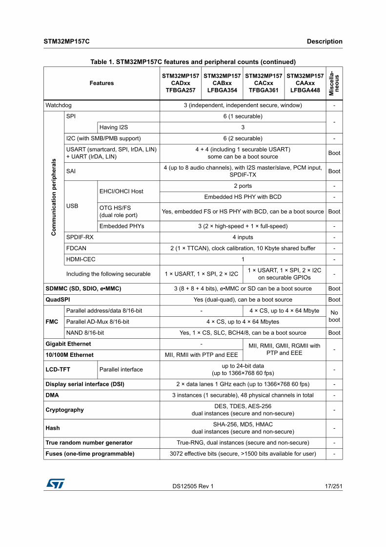
Refer to Table 1: STM32MP157C features and peripheral counts for the list of peripherals available on each part number.
A comprehensive set of power-saving mode allows the design of low-power applications.
The STM32MP157C devices are proposed in 4 packages ranging from 257 to 448 balls with pitch 0.5 mm to 0.8 mm. The set of included peripherals changes with the device chosen.
These features make the STM32MP157C suitable for a wide range of consumer, industrial, white goods and medical applications.
Figure 1 shows the general block diagram of the device family.

Description STM32MP157C
16/251 DS12505 Rev 1
Table 1. STM32MP157C features and peripheral counts
FeaturesSTM32MP157
CADxxTFBGA257
STM32MP157CABxx
LFBGA354
STM32MP157CACxx
TFBGA361
STM32MP157CAAxx
LFBGA448
Mis
cella
-n
eou
s
Package
Body size (mm) 10x10 16x16 12x12 18x18
-
Pitch (mm) 0.5(1) 0.8 0.5(1) 0.8
Ball size (mm) 0.30 0.40 0.30 0.40
Thickness (mm) <1.2 <1.4 <1.2 <1.4
Ball count 257 354 361 448
CPU Dual-core Cortex-A7 FPU Neon TrustZone
-Caches size
2 × 32-Kbyte L1 data cache
2 × 32-Kbyte L1 instruction cache
256-Kbyte level 2 unified coherent cache
Frequency 2 × 650 MHz(2)
GPU Vivante - Open GL ES 2.0-
for 3D graphics Frequency 533 MHz
MCU core Cortex-M4 FPU-
Frequency 209 MHz
ROM 128 Kbytes (secure) -
Embedded SRAM
CPU system 256 Kbytes (securable)
708
Kb
ytes
MCU subsystem 384 Kbytes
MCU retention 64 Kbytes
Backup 4 Kbytes (securable, tamper protected)
SD
RA
M
(sec
ura
ble
)
LPDDR2/3 16-bit 533 MHz
Up to 1 Gbyte, single rank
- Up to 1 Gbyte, single rank
-
-32-bit 533 MHz - - -
DDR3/3L 16-bit 533 MHz Up to 1 Gbyte, single rank
32-bit 533 MHz - -
Backup registers 128 bytes (32x32-bit, securable, tamper protected) -
Tim
ers
Advanced 16 bits 2
29 ti
mer
s
General purpose
16 bits 8
32 bits 2
Basic 16 bits 2
Low power 16 bits 5
A7 timers 64 bits 2 × 4 (secure, non-secure, virtual, hypervisor)
M4 SysTick
24 bits 1
RTC/AWU 1 (securable)
DS12505 Rev 1 17/251
STM32MP157C Description
58
Watchdog 3 (independent, independent secure, window) -
Co
mm
un
ica
tio
n p
eri
ph
eral
s
SPI 6 (1 securable) -
Having I2S 3
I2C (with SMB/PMB support) 6 (2 securable) -
USART (smartcard, SPI, IrDA, LIN) + UART (IrDA, LIN)
4 + 4 (including 1 securable USART)some can be a boot source
Boot
SAI4 (up to 8 audio channels), with I2S master/slave, PCM input,
SPDIF-TXBoot
USB
EHCI/OHCI Host2 ports -
Embedded HS PHY with BCD -
OTG HS/FS (dual role port)
Yes, embedded FS or HS PHY with BCD, can be a boot source Boot
Embedded PHYs 3 (2 × high-speed + 1 × full-speed) -
SPDIF-RX 4 inputs -
FDCAN 2 (1 × TTCAN), clock calibration, 10 Kbyte shared buffer -
HDMI-CEC 1 -
Including the following securable 1 × USART, 1 × SPI, 2 × I2C1 × USART, 1 × SPI, 2 × I2C
on securable GPIOs-
SDMMC (SD, SDIO, e•MMC) 3 (8 + 8 + 4 bits), e•MMC or SD can be a boot source Boot
QuadSPI Yes (dual-quad), can be a boot source Boot
FMC
Parallel address/data 8/16-bit - 4 × CS, up to 4 × 64 Mbyte No bootParallel AD-Mux 8/16-bit 4 × CS, up to 4 × 64 Mbytes
NAND 8/16-bit Yes, 1 × CS, SLC, BCH4/8, can be a boot source Boot
Gigabit Ethernet - MII, RMII, GMII, RGMII with PTP and EEE
-10/100M Ethernet MII, RMII with PTP and EEE
LCD-TFT Parallel interfaceup to 24-bit data
(up to 1366×768 60 fps)-
Display serial interface (DSI) 2 × data lanes 1 GHz each (up to 1366×768 60 fps) -
DMA 3 instances (1 securable), 48 physical channels in total -
CryptographyDES, TDES, AES-256
dual instances (secure and non-secure)-
HashSHA-256, MD5, HMAC
dual instances (secure and non-secure)-
True random number generator True-RNG, dual instances (secure and non-secure) -
Fuses (one-time programmable) 3072 effective bits (secure, >1500 bits available for user) -
Table 1. STM32MP157C features and peripheral counts (continued)
FeaturesSTM32MP157
CADxxTFBGA257
STM32MP157CABxx
LFBGA354
STM32MP157CACxx
TFBGA361
STM32MP157CAAxx
LFBGA448
Mis
cella
-n
eou
s

Description STM32MP157C
18/251 DS12505 Rev 1
Camera interface Bus width 14-bit -
GPIOs with interrupt (total count) 98 148 176
-Securable GPIOs - 8
Wakeup pins 4 6
Tamper pins (active tamper) 2 (1) 3 (1)
DFSDM 8 input channels with 6 filters -
Up to 16-bit synchronized ADC 2 (up to 0.25/4.4/5/5.7/6.7 Msps on 16/14/12/10/8-bit each)
-
Low noise 16 bit (differential) - 2 (1)
16 bit (differential) 6 (1) 7 (1)
14 bit (differential) 11 (3) 13 (3)
ADC channels in total 17 22
12-bit DAC 2 -
Internal ADC/DAC VREF 1.5 V, 1.8 V, 2.048 V, 2.5 V or VREF+ input-
VREF+ input pin Yes
1. With inner matrix balls having 0.65 mm pitch to allow optimized PCB routing for supplies.
2. Limited to 600 MHz when used for industrial application.
Table 1. STM32MP157C features and peripheral counts (continued)
FeaturesSTM32MP157
CADxxTFBGA257
STM32MP157CABxx
LFBGA354
STM32MP157CACxx
TFBGA361
STM32MP157CAAxx
LFBGA448
Mis
cella
-n
eou
s

DS12505 Rev 1 19/251
STM32MP157C Description
58
Figure 1. STM32MP157C block diagram
MSv47445V3
@VDDA
@VDD_ANA
@V
DD
A
@V
SW
@V
DD
@V
SW
@VDDA
@V
SW
OTP Fuses
T
T
T
T
T
@V
SW
SYSRAM 256KB
ROM 128KB
TIM3
ADC1ADC2
64 bits
32 bits
32 bits
AXI
AHB
APB
64bits AXI master
T TrustZone® security protection
@VDDVoltage Regulators
@VDD_ANASupply Supervision
32 bits AHB master
BKPSRAM 4KB
STM
RETSRAM 64KB
DTS (Digital temperature sensor)
@VDD_PLL PLL1/2/3/4
@VDD HSE (XTAL)
RCC
RNG2
DCMI (Camera I/F)
MDIOS
CRC2
HSEM
PWR
SDMMC3OTG (HS/FS)
HASH2
T
USBPHYC(USB 2 x PHY control)
FIFO
16b16bIn
terfa
ce
GPIOA
GPIOB
GPIOC
GPIOD
GPIOE
GPIOF
GPIOG
GPIOH
GPIOI
GPIOJ
GPIOK
16b
16b
16b
16b
16b
16b
16b
16b
16b
16b
8b
SRAM1 128KB
SRAM2 128KB
SRAM3/SRAM4 64K/64K
HSI
CSI LSI
DMA18 Streams
DMA28 Streams
FIFO
FIFO
2
17
4
2014
9
16
16
16
16
16
16
16
16
16
16
8
5
TIM4 16b 5
TIM6 16b
TIM7 16b
TIM12 16b 2
TIM13 16b 1
TIM14 16b 1
TIM2 32b 5
TIM5 32b 5
LPTIM1 16b 4
2
USART2 SmartcardIrDA 5
USART3 SmartcardIrDA 5
PLLUSB
FIFO
FIFO
5
T
4b 10
PH
Y
FIFO
I2C4 / SMBUS
SPI6
USART1
IWDG1
BSEC
ETZPC
3
4
5 SmartcardIrDA FI
FOFI
FO
RTC / AWU
LSE (32kHz XTAL)
TAMP / Backup Regs T2
2
3
RNG1
HASH1
CRC1
T
T
LTDC (LCD)
SDMMC1
31
29
14
SDMMC214
8b
8b
FIFO
FIFO
FIFO
MDMA32 Channels
T
QUADSPI (dual)
DDRCTRLLPDDR2/3DDR3/3L
FMC
asyn
c
37
13
77
GPIOZ8b816b
AHB2APB
Trace port
AP
B1
(104
.5 M
Hz)
AP
B3
(104
.5 M
Hz)
T
24b
8b
AHB2APB
2x2Matrix
AHB2APB
IC Supplies
16b
AXI
M: A
RM
64-
bit A
XI i
nter
conn
ect (
266
MH
z)as
ync
DLYBSD1 (SDMMC1 DLY control)
DLYBSD2 (SDMMC2 DLY control)
DLYBSD3 (SDMMC3 DLY control)
async
DLYBQS (QUADSPI DLY control)
17 16b
FIFO
FIFO
14b
DMAMUX1
DDRPHYC
AXI
MC
T
TT
T
8KB
FI
FO
Sys. Timing GENeration
AP
B5
(133
MH
z)
debug TimeStamp GENerator TSGEN
DLY
DLY
DLY
DLY
(R)(G)MII
32b
PH
Y
AP
B4
MLA
HB
: AR
M 3
2-bi
t mul
ti-A
HB
bus
mat
rix (2
09 M
Hz)
T
@V
SW IWDG2
TI2C6 / SMBUS3
USBH (2 x HS Host)
22 2
x P
HY
FIFO
STGENC
STGENR
EXTI 17616extT
T
T
T
SYSCFG
VREFBUF
TIM1 / PWM
TIM8 / PWM10
10
16b
16b
TIM154 16b
TIM1616b
TIM1716b
3
3
1
LPTIM216b4
LPTIM316b1
LPTIM416b1
LPTIM516b1
SAI413 FIFO
3
HDP8 8b
SAI113 FIFO
SAI28 FIFO
SAI38 FIFO
UART4 4
UART5 4
UART7 4
UART8 4
DAC1DAC2
12b12bIn
terfa
ce 11
I2C1 / SMBUS 3Filte
r
I2C2 / SMBUS 3Filte
r
I2C3 / SMBUS 3Filte
r
I2C5 / SMBUS 3Filte
r
CEC (HDMI-CEC)SPDIFRX
1
4
SPI2 / I2S2
SPI3 / I2S35
5
FIFO
FIFO
FIFO
FIFO
FIFO
FIFO
FIFO
SPI4 4
SPI5 4
USART6 5SmartcardIrDA
FIFO
FIFO
FIFO
SPI1 / I2S1 5FIFO
WWDG1
4ch
DFSDM1 178ch
AHB2APB
BOOTpins
T
T
T
128 bits
CNT (Timer) TETM T
Cortex-A7 CPU 650 MHz + MMU + FPU +
NEON T
32K I$
32K D$ T
ETH1 GMAC 10/100/1000 FI
FODAP (JTAG / SWD)T
T
DDRPERFM
asyn
c
CRYP2
DA
P bu
s
CRYP1
IPCC
T
TZC
T
T
FIFO
GPUas
ync Shader
(533 MHz)
FDCAN1 (TT)
FDCAN2Buffer 10KB CCU
2
2
AP
B2
(104
.5 M
Hz)
APB2 (104.5 MHz)
AP
B2
(104
.5 M
Hz)
PLLDSIDSIP
HY6
I-Bus
D-Bus
S-Bus
SYSTICKNVIC
Cortex-M4 CPU 209 MHz+ MPU + FPU
GIC
ETMCNT (Timer) T
T
Cortex-A7 CPU 650 MHz + MMU + FPU +
NEON T
32K I$32K D$
256K
B L
2$ +
SC
UT
T

Functional overview STM32MP157C
20/251 DS12505 Rev 1
3 Functional overview
3.1 Dual-core Arm® Cortex®-A7 subsystem
3.1.1 Features
• ARMv7-A architecture
• 32-Kbyte L1 instruction cache for each CPU
• 32-Kbyte L1 data cache for each CPU
• 256-Kbyte level2 cache
• Arm® + Thumb®-2 instruction set
• Arm® TrustZone® security technology
• Arm® NEON™ Advanced SIMD
• DSP and SIMD extensions
• VFPv4 floating-point
• Hardware virtualization support
• Embedded trace module (ETM)
• Integrated generic interrupt controller (GIC) with 256 shared peripheral interrupts
• Integrated generic timer (CNT)
3.1.2 Overview
The Cortex-A7 processor is a very energy-efficient applications processor designed to provide rich performance in high-end wearables, and other low-power embedded and consumer applications. It provides up to 20 % more single thread performance than the Cortex-A5 and provides similar performance than the Cortex-A9.
The Cortex-A7 incorporates all features of the high-performance Cortex-A15 and Cortex-A17 processors, including virtualization support in hardware, NEON™, and 128-bit AMBA®4 AXI bus interface.
The Cortex-A7 processor builds on the energy-efficient 8-stage pipeline of the Cortex-A5 processor. It also benefits from an integrated L2 cache designed for low-power, with lower transaction latencies and improved OS support for cache maintenance. On top of this, there is improved branch prediction and improved memory system performance, with 64-bit load-store path, 128-bit AMBA 4 AXI buses and increased TLB size (256 entry, up from 128 entry for Cortex-A9 and Cortex-A5), increasing performance for large workloads such as web browsing.
Thumb-2 technology
Delivers the peak performance of traditional Arm® code while also providing up to a 30 % reduction in memory requirement for instructions storage.
TrustZone technology
Ensures reliable implementation of security applications ranging from digital rights management to electronic payment. Broad support from technology and industry partners.
DS12505 Rev 1 21/251
STM32MP157C Functional overview
58
NEON
NEON technology can accelerate multimedia and signal processing algorithms such as video encode/decode, 2D/3D graphics, gaming, audio and speech processing, image processing, telephony, and sound synthesis. The Cortex-A7 provides an engine that offers both the performance and functionality of the Cortex-A7 floating-point unit (FPU) and an implementation of the NEON advanced SIMD instruction set for further acceleration of media and signal processing functions. The NEON extends the Cortex-A7 processor FPU to provide a quad-MAC and additional 64-bit and 128-bit register set supporting a rich set of SIMD operations over 8-, 16- and 32-bit integer and 32-bit floating-point data quantities.
Hardware virtualization
Highly efficient hardware support for data management and arbitration, whereby multiple software environments and their applications are able to simultaneously access the system capabilities. This enables the realization of devices that are robust, with virtual environments that are well isolated from each other.
Optimized L1 caches
Performance and power optimized L1 caches combine minimal access latency techniques to maximize performance and minimize power consumption. There is also the option of cache coherence for enhanced inter-processor communication, or support of a rich SMP capable OS for simplified multicore software development.
Integrated L2 cache controller
Provides low-latency and high-bandwidth access to cached memory in high-frequency, or to reduce the power consumption associated with off-chip memory access.
Cortex-A7 floating-point unit (FPU)
The FPU provides high-performance single and double precision floating-point instructions compatible with the Arm VFPv4 architecture that is software compatible with previous generations of Arm floating-point coprocessor.
Snoop control unit (SCU)
The SCU is responsible for managing the interconnect, arbitration, communication, cache to cache and system memory transfers, cache coherence and other capabilities for the processor.
This system coherence also reduces software complexity involved in maintaining software coherence within each OS driver.
Generic interrupt controller (GIC)
Implementing the standardized and architected interrupt controller, the GIC provides a rich and flexible approach to inter-processor communication and the routing and prioritization of system interrupts.
Supporting up to 288 independent interrupts, under software control, each interrupt can be distributed across A7 cores, hardware prioritized, and routed between the operating system and TrustZone software management layer.
Functional overview STM32MP157C
22/251 DS12505 Rev 1
This routing flexibility and the support for virtualization of interrupts into the operating system, provides one of the key features required to enhance the capabilities of a solution utilizing a hypervisor.
3.2 Arm® Cortex®-M4 with FPU
The Arm® Cortex®-M4 with FPU core is a 32-bit RISC processor that features exceptional code-efficiency, delivering the high-performance expected from an Arm core in the memory size usually associated with 8- and 16-bit devices.
The processor supports a set of DSP instructions which allow efficient signal processing and complex algorithm execution.
Its single precision FPU (floating point unit) speeds up software development by using metalanguage development tools, while avoiding saturation.
Note: Cortex-M4 with FPU core is binary compatible with the Cortex-M3 core.
Memory protection unit (MPU)
The memory protection unit (MPU) manages the Cortex®-M4 access rights and the attributes of the system resources. It has to be programmed and enabled before use. Its main purposes are to prevent an untrusted user program to accidentally corrupt data used by the OS and/or by a privileged task, but also to protect data processes or read-protect memory regions.
The MPU defines access rules for privileged accesses and user program accesses. It allows the definition of up to 16 protected regions that can in turn be divided into up to 8 independent subregions, where region address, size, and attributes can be configured. The protection area ranges from 32 bytes to 4 Gbytes of addressable memory.When an unauthorized access is performed, a memory management exception is generated.
3.3 Graphic processing unit (GPU)
The STM32MP157C includes a 3D graphics engine (Vivante).
The GPU is a dedicated graphics processing unit accelerating numerous 3D graphics applications such as graphical user interface (GUI), menu display or animations.
It works together with an optimized software stack design for industry-standard APIs with support for Android™ and Linux® embedded development platforms.

DS12505 Rev 1 23/251
STM32MP157C Functional overview
58
Hardware features:
• OpenGL ES 2.0 / 1.1 compliance, including extensions; OpenVG 1.1
• IEEE 32-bit floating-point pipeline
• Ultra-threaded, unified vertex and fragment (pixel) shaders
• Low memory bandwidth at both high and low data rates
• Low CPU loading
• Up to 12 programmable elements per vertex
• Dependent texture operation with high-performance
• Alpha blending
• Depth and stencil compare
• Support for 8 fragment shader simultaneous textures
• Support for 4 vertex shader simultaneous textures
• Point sampling, bi-linear sampling, tri-linear filtering, and cubic textures
• 8 k x 8 k texture size and 8 k x 8 k rendering target
• 4 Vertex DMA streams
API support:
• OpenGL ES 1.1 and 2.0
• OpenVG 1.1
• EGL 1.4
• OpenGL 2.1
Performance up to:
• 26 Mtriangle/s
• 133 Mpixel/s

Functional overview STM32MP157C
24/251 DS12505 Rev 1
3.4 Memories
3.4.1 External SDRAM
The STM32MP157C devices embed a controller for external SDRAM which support the following devices
• LPDDR2 or LPDDR3, 16- or 32-bit data, up to 1 Gbyte, up to 533 MHz clock.
• DDR3 or DDR3L, 16- or 32-bit data, up to 1 Gbyte, up to 533 MHz clock.
3.4.2 Embedded SRAM
All devices feature:
• SYSRAM in MPU domain: 256 Kbytes
• SRAM1 in MCU domain: 128 Kbytes
• SRAM2 in MCU domain: 128 Kbytes
• SRAM3 in MCU domain: 64 Kbytes
• SRAM4 in MCU domain: 64 Kbytes
• RETRAM (retention RAM): 64 Kbytes
The content of this area can be retained in Standby or VBAT mode.
• BKPSRAM (backup SRAM): 4 Kbyte
The content of this area is protected against possible unwanted write accesses, and can be retained in Standby or VBAT mode.
BKPSRAM can be defined (in ETZPC) as accessible by secure software only.

DS12505 Rev 1 25/251
STM32MP157C Functional overview
58
3.5 DDR3/DDR3L/LPDDR2/LPDDR3 controller (DDRCTRL)
DDRCTRL combined with DDRPHYC provides a complete memory interface solution for DDR memory subsystem.
• Two 64-bit AMBA 4 AXI4 ports interface (XPI)
• AXI clock asynchronous to the controller
• Supported standards:
– JEDEC DDR3 SDRAM specification, JESD79-3E for DDR3/3L with 32-bit interface
– JEDEC LPDDR2 SDRAM specification, JESD209-2E for LPDDR2 with 32-bit interface
– JEDEC LPDDR3 SDRAM specification, JESD209-3B for LPDDR3 with 32-bit interface
• Advanced scheduler and SDRAM command generator
• Programmable full data width (32-bit) or half data width (16-bit)
• Advanced QoS support with 3 traffic class on read and 2 traffic classes on write
• Options to avoid starvation of lower priority traffic
• Guaranteed coherency for write-after-read (WAR) and read-after-write (RAW) on AXI ports
• Programmable support for burst length options (4, 8,16)
• Write combine to allow multiple writes to the same address to be combined into a single write
• Single rank configuration
• Supports automatic SDRAM power-down entry and exit caused by lack of transaction arrival for programmable time
• Supports automatic clock stop (LPDDR2/3) entry and exit caused by lack of transaction arrival
• Supports automatic low power mode operation caused by lack of transaction arrival for programmable time via hardware low power interface
• Programmable paging policy
• Supports automatic or under software control self-refresh entry and exit
• Support for deep power-down entry and exit under software control (LPDDR2)
• Support for explicit SDRAM mode register updates under software control
• Flexible address mapper logic to allow application specific mapping of row, column, bank bits
• User-selectable refresh control options
• DDRPERFM associated block to help for performance monitoring and tuning
DDRCTRL and DDRPHYC can be defined (in ETZPC) as accessible by secure software only.

Functional overview STM32MP157C
26/251 DS12505 Rev 1
3.6 TrustZone address space controller for DDR (TZC)
TZC is used to filter read/write accesses to DDR controller according to TrustZone rights and according to non-secure master (NSAID) on up to 9 programmable regions.
• Configuration is supported by trusted software only
• 2 filter units working concurrently 9 regions:
– region 0 is always enabled and covers the whole address range.
– regions 1 to 8 have programmable base/end address and can be assigned to any one or both filters.
• Secure and non-secure access permissions programmed per region
• Non-secure accesses are filtered according to NSAID
• Regions controlled by same filter must not overlap
• Fail modes with error and/or interrupt
• Acceptance capability = 256
• Gate keeper logic to enable and disable of each filter
• Speculative accesses
DS12505 Rev 1 27/251
STM32MP157C Functional overview
58
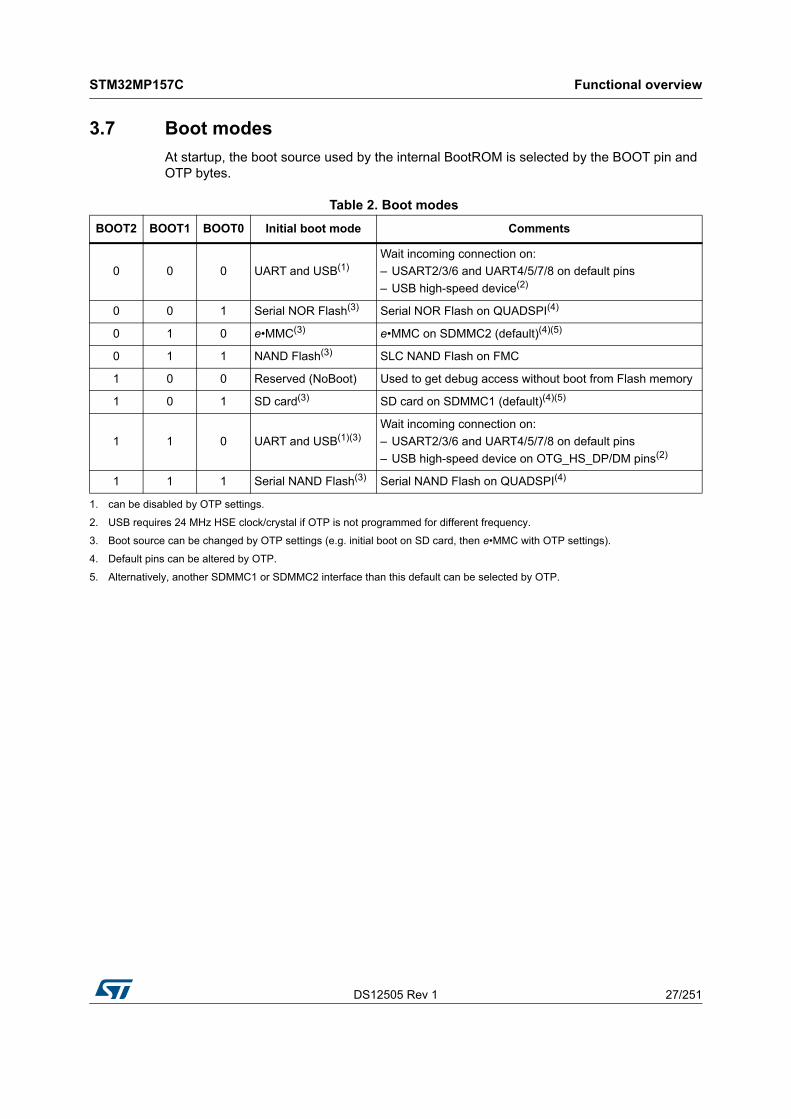
3.7 Boot modes
At startup, the boot source used by the internal BootROM is selected by the BOOT pin and OTP bytes.
Table 2. Boot modes
BOOT2 BOOT1 BOOT0 Initial boot mode Comments
0 0 0 UART and USB(1)Wait incoming connection on:
– USART2/3/6 and UART4/5/7/8 on default pins
– USB high-speed device(2)
0 0 1 Serial NOR Flash(3) Serial NOR Flash on QUADSPI(4)
0 1 0 e•MMC(3) e•MMC on SDMMC2 (default)(4)(5)
0 1 1 NAND Flash(3) SLC NAND Flash on FMC
1 0 0 Reserved (NoBoot) Used to get debug access without boot from Flash memory
1 0 1 SD card(3) SD card on SDMMC1 (default)(4)(5)
1 1 0 UART and USB(1)(3)Wait incoming connection on:
– USART2/3/6 and UART4/5/7/8 on default pins
– USB high-speed device on OTG_HS_DP/DM pins(2)
1 1 1 Serial NAND Flash(3) Serial NAND Flash on QUADSPI(4)
1. can be disabled by OTP settings.
2. USB requires 24 MHz HSE clock/crystal if OTP is not programmed for different frequency.
3. Boot source can be changed by OTP settings (e.g. initial boot on SD card, then e•MMC with OTP settings).
4. Default pins can be altered by OTP.
5. Alternatively, another SDMMC1 or SDMMC2 interface than this default can be selected by OTP.

Functional overview STM32MP157C
28/251 DS12505 Rev 1
3.8 Power supply management
3.8.1 Power supply scheme
• The VDD is the main supply for I/Os and internal part kept powered during Standby mode. Useful voltage range is 1.71 V to 3.6 V (e.g. 1.8 V, 2.5 V, 3.0 V or 3.3 V typ.)
– VDD_DSI, VDD_PLL and VDD_ANA must be star-connected to VDD.
• The VDDCORE is the main digital voltage and is usually shutdown during Standby mode. Voltage range is 1.10 V to 1.28 V (1.2 V typ.).
• The VBAT pin can be connected to the external battery (1.2 V < VBAT < 3.6 V). If no external battery is used, it is mandatory to connect this pin to VDD.
• The VDDA pin is the analog (ADC/DAC/VREF), supply voltage range is 1.71 V to 3.6 V. DAC can only be used when VDDA is above or equal 1.8 V. Using Internal VREF+ requires VDDA equal to or higher than VREF+ + 0.3 V.
• The VDDA1V8_REG pin is the output of internal regulator and connected internally to USB PHY and USB PLL. Internal VDDA1V8_REG regulator is enabled by default and can be controlled by software. It is always shut down during Standby mode.
There is specific BYPASS_REG1V8 pin that must be connected either to VSS or VDD to activate or deactivate the voltage regulator. It is mandatory to bypass the 1.8 V regulator when VDD is below 2.25 V (BYPASS_REG1V8 = VDD). In that case, VDDA1V8_REG pin must be connected to VDD (if below 1.98 V) or to a dedicated 1.65 V - 1.98 V supply (1.8 V typ.).
• VDDA1V8_DSI is the analog DSI supply. Voltage range is 1.65 V to 1.98 V. (1.8 V typ.) Should be connected to VDDA1V8_REG.
• VDDA1V1_REG pin is the output of internal regulator connected internally to USB PHY. Internal VDDA1V1_REG regulator is enabled by default and can be controlled by software. It is always shut down during Standby mode.
• VDDA1V2_DSI_REG pin is the output of internal regulator and connected internally to DSI PLL.
• VDDA1V2_DSI_PHY is the analog DSI PHY supply and should be connected to VDDA1V2_DSI_REG.
• VDD3V3_USBHS and VDD3V3_USBFS are respectively the USB high-speed and full-speed PHY supply. Voltage range is 3.1 V to 3.6 V. VDD3V3_USBFS is used to supply VBUS and ID pins. So, VDD3V3_USBFS must be supplied as well when USB high-speed OTG device is used. If not used, must be connected to VDD.
Caution: VDD3V3_USBHS must not be present unless VDDA1V8_REG is present, otherwise permanent STM32MP157C damage could occur. Must be ensured by PMIC ranking order or with external component in case of discrete component power supply implementation.
• VDDQ_DDR is the DDR IO supply.
– Voltage range is 1.425 V to 1.575 V for interfacing DDR3 memories (1.5 V typ.).
– Voltage range is 1.283 V to 1.45 V for interfacing DDR3L memories (1.35 V typ.).
– Voltage range is 1.14 V to 1.3 V for interfacing LPDDR2 or LPDDR3 memories (1.2 V typ.).
DS12505 Rev 1 29/251
STM32MP157C Functional overview
58
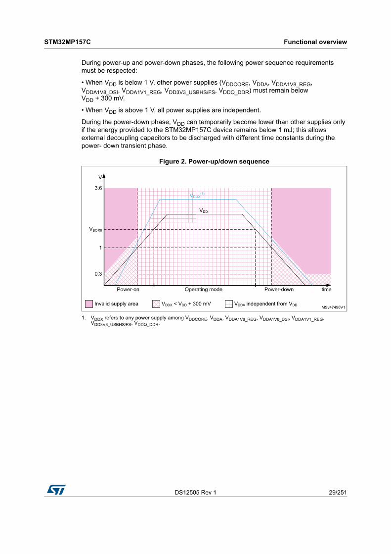
During power-up and power-down phases, the following power sequence requirements must be respected:
• When VDD is below 1 V, other power supplies (VDDCORE, VDDA, VDDA1V8_REG, VDDA1V8_DSI, VDDA1V1_REG, VDD3V3_USBHS/FS, VDDQ_DDR) must remain below VDD + 300 mV.
• When VDD is above 1 V, all power supplies are independent.
During the power-down phase, VDD can temporarily become lower than other supplies only if the energy provided to the STM32MP157C device remains below 1 mJ; this allows external decoupling capacitors to be discharged with different time constants during the power- down transient phase.
Figure 2. Power-up/down sequence
1. VDDX refers to any power supply among VDDCORE, VDDA, VDDA1V8_REG, VDDA1V8_DSI, VDDA1V1_REG, VDD3V3_USBHS/FS, VDDQ_DDR.
MSv47490V1
0.3
1
VBOR0
3.6
Operating modePower-on Power-down time
V
VDDX(1)
VDD
Invalid supply area VDDX < VDD + 300 mV VDDX independent from VDD
Functional overview STM32MP157C
30/251 DS12505 Rev 1
3.8.2 Power supply supervisor
The devices have an integrated power-on reset (POR)/ power-down reset (PDR) circuitry coupled with a Brownout reset (BOR) circuitry:
• Power-on reset (POR)
The POR supervisor monitors VDD power supply and compares it to a fixed threshold. The devices remain in reset mode when VDD is below this threshold,
• Power-down reset (PDR)
The PDR supervisor monitors VDD power supply. A reset is generated when VDD drops below a fixed threshold.
The PDR supervisor can be enabled/disabled through PDR_ON pin.
• Brownout reset (BOR)
The BOR supervisor monitors VDD power supply. Three BOR thresholds (from 2.1 to 2.7 V) can be configured through option bytes. A reset is generated when VDD drops below this threshold.
• Power-on reset VDDCORE (POR_VDDCORE)
The POR_VDDCORE supervisor monitors VDDCORE power supply and compares it to a fixed threshold. The VDDCORE domain remain in reset mode when VDDCORE is below this threshold,
• Power-down reset VDDCORE (PDR_VDDCORE)
The PDR_VDDCORE supervisor monitors VDDCORE power supply. A VDDCORE domain reset is generated when VDDCORE drops below a fixed threshold.
The PDR_VDDCORE supervisor can be enabled/disabled through PDR_ON_CORE pin.
DS12505 Rev 1 31/251
STM32MP157C Functional overview
58
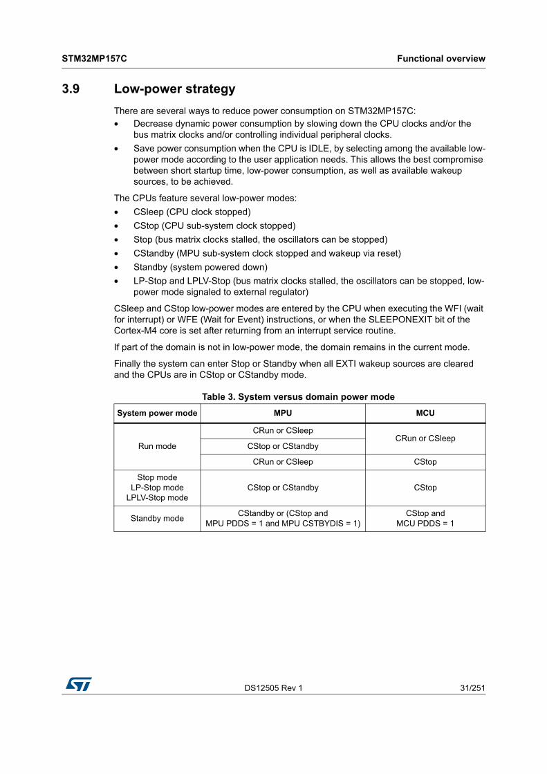
3.9 Low-power strategy
There are several ways to reduce power consumption on STM32MP157C:• Decrease dynamic power consumption by slowing down the CPU clocks and/or the
bus matrix clocks and/or controlling individual peripheral clocks.
• Save power consumption when the CPU is IDLE, by selecting among the available low-power mode according to the user application needs. This allows the best compromise between short startup time, low-power consumption, as well as available wakeup sources, to be achieved.
The CPUs feature several low-power modes:
• CSleep (CPU clock stopped)
• CStop (CPU sub-system clock stopped)
• Stop (bus matrix clocks stalled, the oscillators can be stopped)
• CStandby (MPU sub-system clock stopped and wakeup via reset)
• Standby (system powered down)
• LP-Stop and LPLV-Stop (bus matrix clocks stalled, the oscillators can be stopped, low-power mode signaled to external regulator)
CSleep and CStop low-power modes are entered by the CPU when executing the WFI (wait for interrupt) or WFE (Wait for Event) instructions, or when the SLEEPONEXIT bit of the Cortex-M4 core is set after returning from an interrupt service routine.
If part of the domain is not in low-power mode, the domain remains in the current mode.
Finally the system can enter Stop or Standby when all EXTI wakeup sources are cleared and the CPUs are in CStop or CStandby mode.
Table 3. System versus domain power mode
System power mode MPU MCU
Run mode
CRun or CSleepCRun or CSleep
CStop or CStandby
CRun or CSleep CStop
Stop modeLP-Stop mode
LPLV-Stop modeCStop or CStandby CStop
Standby modeCStandby or (CStop and
MPU PDDS = 1 and MPU CSTBYDIS = 1)CStop and
MCU PDDS = 1

Functional overview STM32MP157C
32/251 DS12505 Rev 1
3.10 Reset and clock controller (RCC)
The clock and reset controller manages the generation of all the clocks, as well as the clock gating and the control of the system and peripheral resets. It provides a high flexibility in the choice of clock sources and allows application of clock ratios to improve the power consumption. In addition, on some communication peripherals that are capable to work with two different clock domains (either a bus interface clock or a kernel peripheral clock), the system frequency can be changed without modifying the baudrate.
3.10.1 Clock management
The devices embed four internal oscillators, two oscillators with external crystal or resonator, three internal oscillators with fast startup time and four PLLs.
The RCC receives the following clock source inputs:
• Internal oscillators:
– 64 MHz HSI clock (1% accuracy)
– 4 MHz CSI clock
– 32 kHz LSI clock
• External oscillators:
– 8-48 MHz HSE clock
– 32.768 kHz LSE clock
The RCC provides four PLLs:
• The PLL1 is dedicated to the MPU clocking
• The PLL2 provides:
– The clocks for the AXI-SS (including APB4, APB5, AHB5 and AHB6 bridges)
– The clocks for the DDR interface
– The clocks for the GPU
• The PLL3 provides:
– The clocks for the MCU, and its bus matrix (including the APB1, APB2, APB3, AHB1, AHB2, AHB3 and AHB4)
– The kernel clocks for peripherals
• The PLL4 is dedicated to the generation of the kernel clocks for various peripherals
The system starts on the HSI clock. The user application can then select the clock configuration.

DS12505 Rev 1 33/251
STM32MP157C Functional overview
58
3.10.2 System reset sources
The power-on reset initializes all registers while the system reset reinitializes the system except for the debug, part of the RCC and power controller status registers, as well as the backup power domain.
An application reset is generated from one of the following sources:
– a reset from NRST pad
– a reset from POR and PDR signal (generally called power-on reset)
– a reset from BOR (generally called brownout)
– a reset from the independent watchdogs 1
– a reset from the independent watchdogs 2
– a software reset from the Cortex-M4 (MCU)
– a software reset from the Cortex-A7 (MPU)
– a failure on HSE, when the clock security system feature is activated
A system reset is generated from one of the following sources:
– An application reset,
– A reset from POR_VDDCORE signal,
– Every time the system exits from Standby.
3.11 Hardware semaphore (HSEM)
The HW semaphore block provides 64 (32-bit) register-based semaphores.
The semaphores can be used to ensure synchronization between different processes running on a core and between different cores. The HSEM provides a non blocking mechanism to lock semaphores in an atomic way. The following functions are provided:
• Locking a semaphore can be done in 2 ways:
– 2-step lock: by writing CoreID and ProcessID to the semaphore, followed by a read check.
– 1-step lock: by reading the CoreID from the semaphore.
• Interrupt generation when a semaphore is freed.
– Each semaphore may generated an interrupt on one of the interrupt lines.
• Semaphore clear protection.
– A semaphore is only cleared when CoreID and ProcessID matches.
• Global semaphore clear per CoreID.
3.12 Inter-processor communication controller (IPCC)The inter-processor communication controller (IPCC) is used for communicating data between two processors.
The IPCC block provides a non blocking signaling mechanism to post and retrieve communication data in an atomic way. It provides the signaling for four channels:
• two channels in the direction from processor 1 to processor 2
• two channels in the opposite direction.

Functional overview STM32MP157C
34/251 DS12505 Rev 1
It is then possible to have two different communication types in each direction.
The IPCC communication data must be located in a common memory, which is not part of the IPCC block.
3.12.1 IPCC main features
• Status signaling for the four channels
– Channel occupied/free flag, also used as lock
• Two interrupt lines per processor
– One for RX channel occupied (communication data posted by sending processor)
– One for TX channel free (communication data retrieved by receiving processor)
• Interrupt masking per channel
– Channel occupied mask
– Channel free mask
• Two channel operation modes
– Simplex (each channel has its own communication data memory location)
– Half duplex (a single channel in associated to a bidirectional communication data information memory location)
3.13 General-purpose input/outputs (GPIOs)
Each of the GPIO pins can be configured by software as output (push-pull or open-drain, with or without pull-up or pull-down), as input (with or without pull-up or pull-down) or as peripheral alternate function. Most of the GPIO pins are shared with digital or analog alternate functions. All GPIOs are high-current-capable and have speed selection to better manage internal noise, power consumption and electromagnetic emission.
After reset, all GPIOs are in analog mode to reduce power consumption.
The I/O configuration can be locked if needed by following a specific sequence in order to avoid spurious writing to the I/Os registers.
Additionally, GPIO pins on port Z can be individually set as secure, which would mean that software accesses to these GPIOs and associated peripherals defined as secure are restricted to secure software running on Cortex-A7.
3.14 TrustZone protection controller (ETZPC)
ETZPC is used to configure TrustZone security of bus masters and slaves with programmable-security attributes (securable resources) such as:
• On-chip SYSRAM with programmable secure region size
• AHB and APB peripherals to be made secure
Notice that by default, SYSRAM and peripheral are set to secure access only, so, not accessible by non-secure masters such as Cortex-M4 or DMA1/DMA2.
ETZPC can also allocate peripherals and SRAM to be accessible only by the Cortex-M4 and/or DMA1/DMA2. This ensures the safe execution of the Cortex-M4 firmware, protected from other masters (e.g. Cortex-A7) unwanted accesses.
DS12505 Rev 1 35/251
STM32MP157C Functional overview
58
3.15 Bus-interconnect matrix
The devices feature an AXI bus matrix, one main AHB bus matrix and bus bridges that allow bus masters to be interconnected with bus slaves (see Figure 3, the dots represent the enabled master/slave connections).

Functional overview STM32MP157C
36/251 DS12505 Rev 1
Figure 3. STM32MP157C bus matrix
MSv47453V2
MCU_AHB2
MCU_AHB_MPU
MCU_AHB_RET
MCU_AHB3
MCU_AHB_MEM2
MCU_AHB4
MCU_AHB_MEM1
MCU_AHB_MEM0
S-B
US
D-B
US
I-BU
SMPU_AXI_FMC
MPU_AXI_QUADSPI
MPU_AXI_SYSRAM
MPU_AXI_DDR1
MPU_AHB_MCU
MPU_AHB6
MPU_AXI_ROM
MPU_AHB5
MPU_APB5
MPU_AXI_STM
MPU_AXI_DDR2
MPU_DBG_APB
128-
bit
Interconnect AHB 32 bits 209 MHz - 10 masters / 9 slaves
NIC-400 AXI 64 bits 266 MHz - 11 masters / 12 slaves
FMC/NAND
DDRCTRL 533 MHz
APB bridge to APB5
APB bridge to DBG APB
QUADSPI
SYSRAM 256 KB
ROM 128 KB
STM
AHB bridge to AHB5
AHB bridge to AHB6
S1
S2
S3
S4
S5
S6
S7
S9
S10
S8
S0
S11
AHB 32 synchronous master port
AXI 64 synchronous master port
AXI 64 synchronous slave port
AXI 64 asynchronous master port
AXI 64 asynchronous slave port
AHB 32 synchronous slave port
AHB 32 asynchronous master port
AHB 32 asynchronous slave port
Masters access S0 XOR S1 layer
SD
MM
C1
MD
MA
LTD
C
Default slave
CP
U
SD
MM
C2
AXI
M
From
MC
U
inte
rcon
nect
ETH
DB
G
US
BH
M0 M1 M2 M3 M4 M5 M6 M7 M9M10
GP
U 5
33 M
Hz
M8
AXIMC
To MCU interconnect
Bridge to AHB3
Bridge to AHB2
RetentionRAM
Bridge to AHB4
SRAM3
S1
S2
S3
S4
S5
S6
S7
S0
US
BO
SD
MM
C3
CM
4
From
MP
U
inte
rcon
nect
DM
A1
M1 M2 M3 M4 M5 M6 M7 M8M0 M9
To MPU interconnect
DM
A2
SRAM1
SRAM2
MLA
HB
MCU_AHB_MEM3SRAM4S8

DS12505 Rev 1 37/251
STM32MP157C Functional overview
58
3.16 DMA controllers
The devices features three DMA modules to unload CPU activity:
• A master direct memory access (MDMA)
The MDMA is a high-speed DMA controller, which is in charge of all types of memory transfers (peripheral to memory, memory to memory, memory to peripheral), without any CPU action. It features a master AXI interface.
The MDMA is located in MPU domain. It is able to interface with the other DMA controllers located in MCU domain to extend the standard DMA capabilities, or can manage peripheral DMA requests directly.
Each of the 32 channels can perform block transfers, repeated block transfers and linked list transfers.
The MDMA can be set to make secure transfers to secured memories.
• Two DMA controllers (DMA1, DMA2), located in MCU domain. Each controller is a dual-port AHB, for a total of 16 DMA channels to perform FIFO-based block transfers.
The DMAMUX is an extension of the DMA1 and DMA2 controllers. It multiplexes and routes the DMA peripheral requests to the DMA1 or DMA2 controllers, with a high flexibility, maximizing the number of DMA requests that run concurrently, as well as generating DMA requests from peripheral output trigger or DMA event.
3.17 Nested vectored interrupt controller (NVIC)
The devices embed a nested vectored interrupt controller able to manage 16 priority levels, and handle up to 150 maskable interrupt channels plus the 16 interrupt lines of the Cortex®-M4 with FPU core.
• Closely coupled NVIC gives low-latency interrupt processing
• Interrupt entry vector table address passed directly to the core
• Allows early processing of interrupts
• Processing of late arriving, higher-priority interrupts
• Support tail chaining
• Processor context automatically saved
• Interrupt entry restored on interrupt exit with no instruction overhead
This hardware block provides flexible interrupt management features with minimum interrupt latency.
3.18 Extended interrupt and event controller (EXTI)
The extended interrupt and event controller (EXTI) manages individual CPU and system wakeup through configurable and direct event inputs. It provides wake-up requests to the power control, and generates an interrupt request to the CPUs NVIC or GIC and events to the CPUs event inputs. For each CPU an additional event generation block (EVG) is needed to generate the CPU event signal.
The EXTI wake-up requests allow the system to be woken up from Stop mode, and the CPUs to be woken up from CStop and CStandby modes.
The interrupt request and event request generation can also be used in Run mode.

Functional overview STM32MP157C
38/251 DS12505 Rev 1
The block also includes the EXTI IOport selection.
Each interrupt or event can be set as secure in order to restrict access to secure software only.
3.19 Cyclic redundancy check calculation unit (CRC1, CRC2)
The CRC (cyclic redundancy check) calculation unit is used to get a CRC code using a programmable polynomial.
Among other applications, CRC-based techniques are used to verify data transmission or storage integrity. In the scope of the EN/IEC 60335-1 standard, they offer a means of verifying the Flash memory integrity. The CRC calculation unit helps computing a signature of the software during runtime, to be compared with a reference signature generated at link-time and stored at a given memory location.
3.20 Flexible memory controller (FMC)
The FMC controller main features are the following:• Interface with static-memory mapped devices including:
– NOR Flash memory
– Static or pseudo-static random access memory (SRAM, PSRAM)
– NAND Flash memory with 4-bit/8-bit BCH hardware ECC
• 8-,16-bit data bus width
• Independent chip select control for each memory bank
• Independent configuration for each memory bank
• Write FIFO
3.21 Dual Quad-SPI memory interface (QUADSPI)
The QUADSPI is a specialized communication interface targeting single, dual or quad SPI Flash memories. It can operate in any of the three following modes:
• indirect mode: all the operations are performed using the QUADSPI registers
• status polling mode: the external Flash memory status register is periodically read and an interrupt can be generated in case of flag setting
• memory-mapped mode: the external Flash memory is mapped to the address space and is seen by the system as if it was an internal memory
Both throughput and capacity can be increased two-fold using dual-flash mode, where two Quad-SPI Flash memories are accessed simultaneously.
QUADSPI is coupled with a delay block (DLYBQS) allowing the support of external data frequency above 100 MHz.
DS12505 Rev 1 39/251
STM32MP157C Functional overview
58
3.22 Analog-to-digital converters (ADCs)
The STM32MP157C devices embed two analog-to-digital converters, which resolution can be configured to 16, 14, 12, 10 or 8 bits. Each ADC shares up to 20 external channels, performing conversions in the single-shot or scan mode. In scan mode, automatic conversion is performed on a selected group of analog inputs.
Additional logic functions embedded in the ADC interface allow:
• simultaneous ADC1/ADC2 conversion
• interleaved ADC1/ADC2 conversion.
The ADC can be served by the DMA controller, thus allowing the automatic transfer of ADC converted values to a destination location without any software action.
In addition, an analog watchdog feature can accurately monitor the converted voltage of one, some or all selected channels. An interrupt is generated when the converted voltage is outside the programmed thresholds.
In order to synchronize A/D conversion and timers, the ADCs can be triggered by any of TIM1, TIM2, TIM3, TIM4, TIM6, TIM8, TIM15, LPTIM1, LPTIM2 and LPTIM3 timers.
3.23 Temperature sensor
The STM32MP157C devices embed a temperature sensor that generates a voltage (VTS) that varies linearly with the temperature. This temperature sensor is internally connected to ADC2_INP12. It can measure the device ambient temperature ranging from –40 to +125 °C with a precision of ±2%.
The temperature sensor has a good linearity, but it has to be calibrated to obtain a good overall accuracy of the temperature measurement. As the temperature sensor offset varies from chip to chip due to process variation, the uncalibrated internal temperature sensor is suitable for applications that detect temperature changes only. To improve the accuracy of the temperature sensor measurement, each device is individually factory-calibrated by ST. The temperature sensor factory calibration data are stored by ST in the OTP area, which is accessible in read-only mode.
3.24 Digital temperature sensor (DTS)
The device embeds a frequency output temperature sensor. This block counts the frequency based on the LSE or PCLK to provide the temperature information.
Following functions can be supported:
• Interrupt generation by temperature threshold.
• Wakeup signal generation by temperature threshold.
3.25 VBAT operation
The VBAT power domain contains the RTC, the backup registers, the retention RAM and the backup SRAM.

Functional overview STM32MP157C
40/251 DS12505 Rev 1
In order to optimize battery duration, this power domain is supplied by VDD when available or by the voltage applied on VBAT pin (when VDD supply is not present). VBAT power is switched when the PDR detects that VDD has dropped below the PDR level.
The voltage on the VBAT pin could be provided by an external battery, a supercapacitor or directly by VDD. In the later case, VBAT mode is not functional.
VBAT operation is activated when VDD is not present.
The VBAT pin supplies the RTC, the backup registers, the retention RAM and the backup SRAM.
Note: None of these events: external interrupts, TAMP event, or RTC alarm/events are able to directly restore the VDD supply and force the STM32MP157C device out of the VBAT
operation. Nevertheless, TAMP events and RTC alarm/events can be used to generate a signal to an external circuitry (typically a PMIC) that can restore the STM32MP157C VDD supply.
When PDR_ON pin is connected to VSS (internal reset OFF), the VBAT functionality is no more available and VBAT pin must be connected to VDD.
3.26 Digital-to-analog converters (DAC1, DAC2)
The two 12-bit buffered DAC channels can be used to convert two digital signals into two analog voltage signal outputs.
This dual digital interface supports the following features:
• Two DAC converters: one for each output channel
• 8-bit or 12-bit monotonic output
• Left or right data alignment in 12-bit mode
• Synchronized update capability
• Noise-wave generation
• Triangular-wave generation
• Sample and hold mode to reduce the power consumption
• Dual DAC channel independent or simultaneous conversions
• DMA capability for each channel including DMA underrun error detection
• External triggers for conversion
• input voltage reference VREF+ or internal VREFBUF reference.
The DAC channels are triggered through the timer update outputs that are also connected to different DMA streams.
DS12505 Rev 1 41/251
STM32MP157C Functional overview
58
3.27 Voltage reference buffer (VREFBUF)
The STM32MP157C devices embed a voltage reference buffer which can be used as voltage reference for ADC, DACs and also as voltage reference for external components through the VREF+ pin.
The internal voltage reference buffer supports four voltages:
• 1.5 V
• 1.8 V
• 2.048 V
• 2.5 V
An external voltage reference can be provided through the VREF+ pin when the internal voltage reference buffer is off.
Figure 4. Voltage reference buffer
3.28 Digital filter for sigma delta modulators (DFSDM1)
The device embeds one DFSDM with support for 6 digital filters modules and 8 external input serial channels (transceivers) or alternately 8 internal parallel inputs.
The DFSDM peripheral is dedicated to interface external Σ∆ modulators to STM32MP157C and perform digital filtering of the received data streams. Σ∆ modulators are used to convert analog signals into digital serial streams that constitute the inputs of the DFSDM. The DFSDM can also interface PDM (pulse density modulation) microphones and perform the PDM to PCM conversion and filtering (hardware accelerated). The DFSDM features optional parallel data stream inputs from internal ADC peripherals or STM32MP157C memory (through DMA/CPU transfers into DFSDM).
The DFSDM transceivers support several serial interface formats (to support various Σ∆ modulators). DFSDM digital filter modules perform digital processing according user-defined filter parameters with up to 24-bit final ADC resolution.
MSv40197V1
VREFBUF
Low frequency cut-off capacitor
DAC, ADC
Bandgap +
VDDA
-
100 nF
VREF+

Functional overview STM32MP157C
42/251 DS12505 Rev 1
The DFSDM peripheral supports:
• 8 multiplexed input digital serial channels:
– configurable SPI interface to connect various SD modulator(s)
– configurable Manchester coded 1-wire interface support
– PDM (pulse density modulation) microphone input support
– maximum input clock frequency up to 20 MHz (10 MHz for Manchester coding)
– clock output for SD modulator(s): 0…20 MHz
• Alternative inputs from 8 internal digital parallel channels (up to 16-bit input resolution):
– internal sources: ADC data or memory data streams (DMA)
• 6 digital filter modules with adjustable digital signal processing:
– Sincx filter: filter order/type (1…5), oversampling ratio (1…1024)
– integrator: oversampling ratio (1…256)
• Up to 24-bit output data resolution, signed output data format
• Automatic data offset correction (offset stored in register by user)
• Continuous or single conversion
• Start-of-conversion triggered by:
– software trigger
– internal timers
– external events
– start-of-conversion synchronously with first digital filter module (DFSDM0)
• Analog watchdog feature:
– low value and high value data threshold registers
– dedicated configurable Sincx digital filter (order = 1…3, oversampling ratio = 1…32)
– input from final output data or from selected input digital serial channels
– continuous monitoring independently from standard conversion
• Short circuit detector to detect saturated analog input values (bottom and top range):
– up to 8-bit counter to detect 1…256 consecutive 0’s or 1’s on serial data stream
– monitoring continuously each input serial channel
• Break signal generation on analog watchdog event or on short circuit detector event
• Extremes detector:
– storage of minimum and maximum values of final conversion data
– refreshed by software
• DMA capability to read the final conversion data
• Interrupts: end of conversion, overrun, analog watchdog, short circuit, input serial channel clock absence
• “Regular” or “injected” conversions:
– “regular” conversions can be requested at any time or even in continuous mode without having any impact on the timing of “injected” conversions
– “injected” conversions for precise timing and with high conversion priority

DS12505 Rev 1 43/251
STM32MP157C Functional overview
58
3.29 Digital camera interface (DCMI)
The devices embed a camera interface that can connect with camera modules and CMOS sensors through an 8-bit to 14-bit parallel interface, to receive video data. The camera interface can achieve a data transfer rate up to 140 Mbyte/s using a 80 MHz pixel clock and 14-bit of data. It features:
• Programmable polarity for the input pixel clock and synchronization signals
• Parallel data communication can be 8-, 10-, 12- or 14-bit
• Supports 8-bit progressive video monochrome or raw Bayer format, YCbCr 4:2:2 progressive video, RGB 565 progressive video or compressed data (like JPEG)
• Supports continuous mode or snapshot (a single frame) mode
• Capability to automatically crop the image
3.30 LCD-TFT display controller (LTDC)
The LCD-TFT display controller provides a 24-bit parallel digital RGB (Red, Green, Blue) and delivers all signals to interface directly to a broad range of LCD and TFT panels up to WXGA (1366×768) @60 fps resolution with the following features:
• 2 display layers with dedicated FIFO
• Color look-up table (CLUT) up to 256 colors (256×24-bit) per layer
• Up to 8 input color formats selectable per layer
• Flexible blending between two layers using alpha value (per pixel or constant)
• Flexible programmable parameters for each layer
• Color keying (transparency color)
• Up to 4 programmable interrupt events
• AXI master interface

Functional overview STM32MP157C
44/251 DS12505 Rev 1
3.31 Display serial interface (DSI)
The display serial interface (DSI) is part of a group of communication protocols defined by the MIPI® Alliance. The MIPI® DSI host controller is a digital core that implements all protocol functions defined in the MIPI® DSI specification.
It provides an interface between the system and the MIPI® D-PHY, allowing the communication with a DSI-compliant display.
• Compliant with MIPI® Alliance standards
• Interface with MIPI® D-PHY
• Supports all commands defined in the MIPI® Alliance specification for DCS
• Supports up to two D-PHY data lanes at 1 Gbps
• Bidirectional communication and escape mode support through data lane 0
• Supports non-continuous clock in D-PHY clock lane for additional power saving
• Supports ultra-low-power mode with PLL disabled
• ECC and checksum capabilities
• Support for end of transmission packet (EoTp)
• Fault recovery schemes
• Configurable selection of system interfaces:
– AMBA APB for control and optional support for generic and DCS commands
– Video mode interface through LTDC
– Adapted command mode interface through LTDC
– Independently programmable virtual channel ID in video mode, adapted command mode and APB slave
• Video mode interfaces features:
– LTDC interface color coding mappings into 16, 18 and 24-bit interface
– Programmable polarity of all LTDC interface signals
– Maximum resolution is limited by available DSI physical link bandwidth
• Adapted interface features:
– Support for sending large amounts of data through the memory_write_start (WMS) and memory_write_continue (WMC) DCS commands
– LTDC interface color coding mappings into 16, 18 and 24-bit interface
• Video mode pattern generator
3.32 True random number generator (RNG1, RNG2)
All the devices embed two RNG that deliver 32-bit random numbers generated by an integrated analog circuit.
RNG1 can be defined (in ETZPC) as accessible by secure software only.

DS12505 Rev 1 45/251
STM32MP157C Functional overview
58
3.33 Cryptographic and hash processors (CRYP1, CRYP2 and HASH1, HASH2)
The devices embed two cryptographic processors that support the advanced cryptographic algorithms usually required to ensure confidentiality, authentication, data integrity and non-repudiation when exchanging messages with a peer:
• Encryption/decryption
– DES/TDES (data encryption standard/triple data encryption standard): ECB (electronic codebook) and CBC (cipher block chaining) chaining algorithms, 64-, 128- or 192-bit key
– AES (advanced encryption standard): ECB, CBC, GCM, CCM, and CTR (counter mode) chaining algorithms, 128, 192 or 256-bit key
• Universal HASH
– SHA-1, SHA224 and SHA256 (secure HASH algorithms)
– MD5
– HMAC
The cryptographic accelerator supports DMA request generation.
CRYP1 and HASH1 can be defined (in ETZPC) as accessible by secure software only.
3.34 Boot and security and OTP control (BSEC)
The BSEC (boot and security and OTP control) is intended to control an OTP (one time programmable) fuse box, used for embedded non-volatile storage for device configuration and security parameters. Some part of BSEC should be configured as accessible by secure software only.
3.35 Timers and watchdogs
The devices include two advanced-control timers, ten general-purpose timers, two basic timers, five low-power timers, three watchdogs, a SysTick timer in Cortex-M4 and 4 system timers in each Cortex-A7.
All timer counters can be frozen in debug mode.
Table 4 compares the features of the advanced-control, general-purpose, basic and low-power timers.

Functional overview STM32MP157C
46/251 DS12505 Rev 1
Table 4. Timer feature comparison
Timertype
TimerCounter
resolutionCounter
typePrescaler
factor
DMArequest
generation
Capture/comparechannels
Comple-mentaryoutput
Maxinterface
clock(MHz)
Maxtimerclock
(MHz)(1)
Advanced-control
TIM1,TIM8
16-bitUp,
down,up/down
Any integerbetween 1and 65536
Yes 4 Yes 100 209
Generalpurpose
TIM2,TIM5
32-bitUp,
down,up/down
Any integer between 1 and 65536
Yes 4 No 100 209
TIM3,TIM4
16-bitUp,
down,up/down
Any integer between 1 and 65536
Yes 4 No 100 209
TIM12 16-bit UpAny integer between 1 and 65536
No 2 No 100 209
TIM13,TIM14
16-bit UpAny integer between 1 and 65536
No 1 No 100 209
TIM15 16-bit UpAny integer between 1 and 65536
Yes 2 1 100 209
TIM16,TIM17
16-bit UpAny integer between 1 and 65536
Yes 1 1 100 209
BasicTIM6,TIM7
16-bit UpAny integer between 1 and 65536
Yes 0 No 100 209
Low-power
LPTIM1,LPTIM2,LPTIM3,LPTIM4,LPTIM5
16-bit Up1, 2, 4, 8, 16, 32, 64,
128No 0 No 100 209
1. The maximum timer clock is up to 209 MHz depending on TIMGxPRE bit in the RCC.
DS12505 Rev 1 47/251
STM32MP157C Functional overview
58
3.35.1 Advanced-control timers (TIM1, TIM8)
The advanced-control timers (TIM1, TIM8) can be seen as three-phase PWM generators multiplexed on 6 channels. They have complementary PWM outputs with programmable inserted dead times. They can also be considered as complete general-purpose timers. Their 4 independent channels can be used for:
• Input capture
• Output compare
• PWM generation (edge- or center-aligned modes)
• One-pulse mode output
If configured as standard 16-bit timers, they have the same features as the general-purpose timers. If configured as 16-bit PWM generators, they have full modulation capability (0-100%).
The advanced-control timer can work together with the general-purpose timers via the timer link feature for synchronization or event chaining.
TIM1 and TIM8 support independent DMA request generation.
3.35.2 General-purpose timers (TIM2, TIM3, TIM4, TIM5, TIM12, TIM13, TIM14, TIM15, TIM16, TIM17)
There are ten synchronizable general-purpose timers embedded in the STM32MP157C devices (see Table 4 for differences).
• TIM2, TIM3, TIM4, TIM5
The devices include 4 full-featured general-purpose timers: TIM2, TIM3, TIM4 and TIM5. TIM2 and TIM5 are based on a 32-bit auto-reload up/downcounter and a 16-bit prescaler while TIM3 and TIM4 are based on a 16-bit auto-reload up/downcounter and a 16-bit prescaler. All timers feature 4 independent channels for input capture/output compare, PWM or one-pulse mode output. This gives up to 16 input capture/output compare/PWMs on the largest packages.
TIM2, TIM3, TIM4 and TIM5 general-purpose timers can work together, or with the other general-purpose timers and the advanced-control timers TIM1 and TIM8 via the timer link feature for synchronization or event chaining.
Any of these general-purpose timers can be used to generate PWM outputs.
TIM2, TIM3, TIM4, TIM5 all have independent DMA request generation. They are capable of handling quadrature (incremental) encoder signals and the digital outputs from 1 to 4 hall-effect sensors.
• TIM12, TIM13, TIM14, TIM15, TIM16, TIM17
These timers are based on a 16-bit auto-reload upcounter and a 16-bit prescaler. TIM13, TIM14, TIM16 and TIM17 feature one independent channel, whereas TIM12 and TIM15 have two independent channels for input capture/output compare, PWM or one-pulse mode output. They can be synchronized with the TIM2, TIM3, TIM4, TIM5 full-featured general-purpose timers or used as simple timebases.
Functional overview STM32MP157C
48/251 DS12505 Rev 1
3.35.3 Basic timers TIM6 and TIM7
These timers are mainly used for DAC trigger and waveform generation. They can also be used as a generic 16-bit time base.
TIM6 and TIM7 support independent DMA request generation.
3.35.4 Low-power timer (LPTIM1, LPTIM2, LPTIM3, LPTIM4, LPTIM5)
The low-power timer has an independent clock and is running also in Stop mode if it is clocked by LSE, LSI or an external clock. It is able to wakeup the device from Stop mode.
These low-power timer supports the following features:
• 16-bit up counter with 16-bit autoreload register
• 16-bit compare register
• Configurable output: pulse, PWM
• Continuous / one-shot mode
• Selectable software / hardware input trigger
• Selectable clock source:
• Internal clock source: LSE, LSI, HSI or APB clock
• External clock source over LPTIM input (working even with no internal clock source running, used by the pulse counter application)
• Programmable digital glitch filter
• Encoder mode
3.35.5 Independent watchdog (IWDG1, IWDG2)
The independent watchdog is based on a 12-bit downcounter and 8-bit prescaler. It is clocked from an independent 32 kHz internal RC(LSI) and as it operates independently from the main clock, it can operate in Stop and Standby modes. It can be used either as a watchdog to reset the device when a problem occurs, or as a free-running timer for application timeout management. It is hardware- or software-configurable through the option bytes.
IWDG1 can be defined (in ETZPC) as accessible by secure software only.
3.35.6 System window watchdog (WWDG1)
The window watchdog is based on a 7-bit downcounter that can be set as free-running. It can be used as a watchdog to reset the device when a problem occurs. It is clocked from the APB clock. It has an early warning interrupt capability and the counter can be frozen in debug mode.
3.35.7 SysTick timer (Cortex-M4)
This timer is embedded inside Cortex-M4 core and dedicated to real-time operating systems, but can also be used as a standard downcounter. It features:
• A 24-bit downcounter
• Autoreload capability
• Maskable system interrupt generation when the counter reaches 0
• Programmable clock source.
DS12505 Rev 1 49/251
STM32MP157C Functional overview
58
3.35.8 Generic timers (Cortex-A7 CNT)
Cortex-A7 generic timers embedded inside Cortex-A7 are fed by value from system timing generation (STGEN).
The Cortex-A7 processor provides a set of four timers for each processor:
• Physical timer for use in secure and non-secure modes. The registers for the physical timer are banked to provide secure and non-secure copies.
• Virtual timer for use in non-secure modes.
• Physical timer for use in hypervisor mode.
Generic timers are not memory mapped peripherals, they are accessible only by specific Cortex-A7 coprocessor instructions (cp15).
3.36 System timer generation (STGEN)
The system timing generation (STGEN) generates a time count value that provides a consistent view of time for all Cortex-A7 generic timers.
The system timing generation has the following key features:
• 64-bit wide to avoid roll-over issues.
• Starts from zero or a programmable value.
• A control APB interface (STGENC) enables the timer to be saved and restored across powerdown events.
• Read-only APB interface (STGENR) enables the timer value to be read by non-secure software and debug tools.
• The timer value incrementing can be stopped during system debug.
STGENC can be defined (in ETZPC) as accessible by secure software only.
3.37 Real-time clock (RTC)
The RTC provides an automatic wakeup to manage all low-power modes.
The real-time clock (RTC) is an independent BCD timer/counter. The RTC provides a time-of-day clock/calendar with programmable alarm interrupts.
The RTC includes also a periodic programmable wakeup flag with interrupt capability.
Two 32-bit registers contain the seconds, minutes, hours (12- or 24-hour format), day (day of week), date (day of month), month, and year, expressed in binary coded decimal format (BCD). The sub-seconds value is also available in binary format.
Compensations for 28-, 29- (leap year), 30-, and 31-day months are performed automatically. Daylight saving time compensation can also be performed.
Additional 32-bit registers contain the programmable alarm subseconds, seconds, minutes, hours, day, and date.
A digital calibration feature is available to compensate for any deviation in crystal oscillator accuracy.
After backup domain reset, all RTC registers are protected against possible parasitic write accesses.
Functional overview STM32MP157C
50/251 DS12505 Rev 1
As long as the supply voltage remains in the operating range, the RTC never stops, regardless of the device status (Run mode, Low-power mode or under reset).
The RTC unit main features are the following:
• Calendar with subseconds, seconds, minutes, hours (12 or 24 format), day (day of week), date (day of month), month, and year.
• Daylight saving compensation programmable by software.
• Programmable alarm with interrupt function. The alarm can be triggered by any combination of the calendar fields.
• Automatic wakeup unit generating a periodic flag that triggers an automatic wakeup interrupt.
• Reference clock detection: a more precise second source clock (50 or 60 Hz) can be used to enhance the calendar precision.
• Accurate synchronization with an external clock using the subsecond shift feature.
• Digital calibration circuit (periodic counter correction): 0.95 ppm accuracy, obtained in a calibration window of several seconds
• Timestamp function for event saving
• Maskable interrupts/events:
– Alarm A
– Alarm B
– Wakeup interrupt
– Timestamp
• TrustZone support:
– RTC fully securable
– Alarm A, alarm B, wakeup timer and timestamp individual secure or non-secure configuration
3.38 Tamper and backup registers (TAMP)
32 x 32-bit backup registers are retained in all low-power modes and also in VBAT mode. They can be used to store sensitive data as their content is protected by an tamper detection circuit. 3 tamper pins and 5 internal tampers are available for anti-tamper detection. The external tamper pins can be configured for edge detection, edge and level, level detection with filtering, or active tamper which increases the security level by auto checking that the tamper pins are not externally opened or shorted.

DS12505 Rev 1 51/251
STM32MP157C Functional overview
58
TAMP main features
• 32 backup registers:
– the backup registers (TAMP_BKPxR) are implemented in the RTC domain that remains powered-on by VBAT when the VDD power is switched off.
• 3 external tamper detection events.
– Each external event can be configured to be active or passive.
– External passive tampers with configurable filter and internal pull-up.
• 5 internal tamper events.
• Any tamper detection can generate a RTC timestamp event.
• Any tamper detection erases the backup registers.
• TrustZone support:
– Tamper secure or non-secure configuration.
– Backup registers configuration in 3 configurable-size areas:
1 read/write secure area.
1 write secure/read non-secure area.
1 read/write non-secure area.
• Monotonic counter.

Functional overview STM32MP157C
52/251 DS12505 Rev 1
3.39 Inter-integrated circuit interface (I2C1, I2C2, I2C3, I2C4, I2C5, I2C6)
The STM32MP157C embeds six I2C interfaces.
The I2C bus interface handles communications between the STM32MP157C and the serial I2C bus. It controls all I2C bus-specific sequencing, protocol, arbitration and timing.
The I2C peripheral supports:
• I2C-bus specification and user manual rev. 5 compatibility:
– Slave and master modes, multimaster capability
– Standard-mode (Sm), with a bitrate up to 100 kbit/s
– Fast-mode (Fm), with a bitrate up to 400 kbit/s
– Fast-mode Plus (Fm+), with a bitrate up to 1 Mbit/s and 20 mA output drive I/Os
– 7-bit and 10-bit addressing mode, multiple 7-bit slave addresses
– Programmable setup and hold times
– Optional clock stretching
• System management bus (SMBus) specification rev 2.0 compatibility:
– Hardware PEC (packet error checking) generation and verification with ACK control
– Address resolution protocol (ARP) support
– SMBus alert
• Power system management protocol (PMBus™) specification rev 1.1 compatibility
• Independent clock: a choice of independent clock sources allowing the I2C communication speed to be independent from the PCLK reprogramming.
• Wakeup from Stop mode on address match
• Programmable analog and digital noise filters
• 1-byte buffer with DMA capability
I2C4 and I2C6 can be defined (in ETZPC) as accessible by secure software only.
3.40 Universal synchronous asynchronous receiver transmitter (USART1, USART2, USART3, USART6 and UART4, UART5, UART7, UART8)
The STM32MP157C devices have four embedded universal synchronous receiver transmitters (USART1, USART2, USART3 and USART6) and four universal asynchronous receiver transmitters (UART4, UART5, UART7 and UART8). Refer to Table 5 for a summary of USARTx and UARTx features.
These interfaces provide asynchronous communication, IrDA SIR ENDEC support, multiprocessor communication mode, single-wire half-duplex communication mode and have LIN master/slave capability. They provide hardware management of the CTS and RTS signals, and RS485 Driver Enable. They are able to communicate at speeds of up to 10 Mbit/s.
USART1, USART2, USART3 and USART6 also provide Smartcard mode (ISO 7816 compliant) and SPI-like communication capability.

DS12505 Rev 1 53/251
STM32MP157C Functional overview
58
All USART have a clock domain independent from the CPU clock, allowing the USARTx to wake up the STM32MP157C from Stop mode using baudrates up to 200 Kbaud.The wake up events from Stop mode are programmable and can be:
• Start bit detection
• Any received data frame
• A specific programmed data frame
All USART interfaces can be served by the DMA controller.
USART1 can be defined (in ETZPC) as accessible by secure software only.
3.41 Serial peripheral interface (SPI1, SPI2, SPI3, SPI4, SPI5, SPI6)– inter- integrated sound interfaces (I2S1, I2S2, I2S3)
The devices feature up to six SPIs (SPI2S1, SPI2S2, SPI2S3, SPI4, SPI5 and SPI6) that allow communication at up to 50 Mbit/s in master and slave modes, in half-duplex, full-duplex and simplex modes. The 3-bit prescaler gives 8 master mode frequencies and the frame is configurable from 4 to 16 bits. All SPI interfaces support NSS pulse mode, TI mode, hardware CRC calculation and 8x 8-bit embedded Rx and Tx FIFOs with DMA capability.
Three standard I2S interfaces (I2S1, I2S2, I2S3, multiplexed with SPI1, SPI2 and SPI3) are available. They can be operated in master or slave mode, in full-duplex and half-duplex communication modes, and can be configured to operate with a 16-/32-bit resolution as an input or output channel. Audio sampling frequencies from 8 kHz up to 192 kHz are supported. When either or both of the I2S interfaces is/are configured in master mode, the master clock can be output to the external DAC/CODEC at 256 times the sampling
Table 5. USART features
USART modes/features(1)
1. X = supported.
USART1/2/3/6 UART4/5/7/8
Hardware flow control for modem X X
Continuous communication using DMA X X
Multiprocessor communication X X
Synchronous mode (master/slave) X -
Smartcard mode X -
Single-wire half-duplex communication X X
IrDA SIR ENDEC block X X
LIN mode X X
Dual clock domain and wakeup from low power mode X X
Receiver timeout interrupt X X
Modbus communication X X
Auto baud rate detection X X
Driver Enable X X
USART data length 7, 8 and 9 bits
Functional overview STM32MP157C
54/251 DS12505 Rev 1
frequency. All I2S interfaces support 16x 8-bit embedded Rx and Tx FIFOs with DMA capability.
SPI6 can be defined (in ETZPC) as accessible by secure software only.
3.42 Serial audio interfaces (SAI1, SAI2, SAI3, SAI4)
The devices embed 4 SAIs that allow the design of many stereo or mono audio protocols such as I2S, LSB or MSB-justified, PCM/DSP, TDM or AC’97. An SPDIF output is available when the audio block is configured as a transmitter. To bring this level of flexibility and reconfigurability, the SAI contains two independent audio sub-blocks. Each block has it own clock generator and I/O line controller. Audio sampling frequencies up to 192 kHz are supported.In addition, up to 8 microphones can be supported thanks to an embedded PDM interface.The SAI can work in master or slave configuration. The audio sub-blocks can be either receiver or transmitter and can work synchronously or asynchronously (with respect to the other one). The SAI can be connected with other SAIs to work synchronously.
3.43 SPDIF receiver interface (SPDIFRX)
The SPDIFRX peripheral is designed to receive an S/PDIF flow compliant with IEC-60958 and IEC-61937. These standards support simple stereo streams up to high sample rate, and compressed multi-channel surround sound, such as those defined by Dolby or DTS (up to 5.1).
The main SPDIFRX features are the following:
• Up to 4 inputs available
• Automatic symbol rate detection
• Maximum symbol rate: 12.288 MHz
• Stereo stream from 32 to 192 kHz supported
• Supports audio IEC-60958 and IEC-61937, consumer applications
• Parity bit management
• Communication using DMA for audio samples
• Communication using DMA for control and user channel information
• Interrupt capabilities
The SPDIFRX receiver provides all the necessary features to detect the symbol rate, and decode the incoming data stream. The user can select the wanted SPDIF input, and when a valid signal is available, the SPDIFRX re-samples the incoming signal, decode the Manchester stream, recognize frames, sub-frames and blocks elements. It delivers to the CPU decoded data, and associated status flags.
The SPDIFRX also offers a signal named spdif_frame_sync, which toggles at the S/PDIF sub-frame rate that is used to compute the exact sample rate for clock drift algorithms.

DS12505 Rev 1 55/251
STM32MP157C Functional overview
58
3.44 Management data input/output (MDIOS)
The devices embed a MDIO slave interface. It includes the following features:
• 32 MDIO register addresses, each of which is managed using separate input and output data registers:
– 32 x 16-bit firmware read/write, MDIO read-only output data registers
– 32 x 16-bit firmware read-only, MDIO write-only input data registers
• Configurable slave (port) address
• Independently maskable interrupts/events:
– MDIO register write
– MDIO register read
– MDIO protocol error
• Able to operate in and wake up from Stop mode
3.45 Secure digital input/output MultiMediaCard interface (SDMMC1, SDMMC2, SDMMC3)
Three secure digital input/output MultiMediaCard interfaces (SDMMC) provide an interface between the AHB bus and SD memory cards, SDIO cards and MMC devices.
The SDMMC features include the following:
• Full compliance with MultiMediaCard System Specification Version 4.51. Card support for three different databus modes: 1-bit (default), 4-bit and 8-bit.
• Full compatibility with previous versions of MultiMediaCards (backward compatibility).
• Full compliance with SD memory card specifications version 4.1. (SDR104 SDMMC_CK speed limited to maximum allowed I/O speed, SPI mode and UHS-II mode not supported).
• Full compliance with SDIO card specification version 4.0. Card support for two different databus modes: 1-bit (default) and 4-bit. (SDR104 SDMMC_CK speed limited to maximum allowed I/O speed, SPI mode and UHS-II mode not supported).
• Data transfer up to 208 Mbyte/s for the 8-bit mode. (depending maximum allowed I/O speed).
• Data and command output enable signals to control external bidirectional drivers.
• The SDMMC host interface embeds a dedicated DMA controller allowing high-speed transfers between the interface and the SRAM.
• IDMA linked list support
Each SDMMC is coupled with a delay block (DLYBSD) allowing support of an external data frequency above 100 MHz.
3.46 Controller area network (FDCAN1, FDCAN2)
The controller area network (CAN) subsystem consists of two CAN modules, a shared message RAM memory and a clock calibration unit.

Functional overview STM32MP157C
56/251 DS12505 Rev 1
Both CAN modules (FDCAN1 and FDCAN2) are compliant with ISO 11898-1 (CAN protocol specification version 2.0 part A, B) and CAN FD protocol specification version 1.0.
FDCAN1 supports time triggered CAN (TTCAN) specified in ISO 11898-4, including event synchronized time-triggered communication, global system time, and clock drift compensation. The FDCAN1 contains additional registers, specific to the time triggered feature. The CAN FD option can be used together with event-triggered and time-triggered CAN communication.
A 10 Kbyte message RAM memory implements filters, receive FIFOs, receive buffers, transmit event FIFOs, transmit buffers (and triggers for TTCAN). This message RAM is shared between the two FDCAN1 and FDCAN2 modules.
The common clock calibration unit is optional. It can be used to generate a calibrated clock for both FDCAN1 and FDCAN2 from the HSI internal RC oscillator and the PLL, by evaluating CAN messages received by the FDCAN1.
3.47 Universal serial bus high-speed host (USBH)
The devices embed one USB high-speed host (up to 480 Mbit/s) with two physical ports. USBH supports both low, full-speed (OHCI) as well as high-speed (EHCI) operations independently on each port. It integrates two transceivers which can be used for either low-speed (1.2 Mbit/s), full-speed (12 Mbit/s) or high-speed operation (480 Mbit/s), the second high-speed transceiver is shared with OTG high-speed.
The USB HS is compliant with the USB 2.0 specification. The USB HS controllers require dedicated clocks that are generated by a PLL inside the USB high-speed PHY.
3.48 USB on-the-go high-speed (OTG)
The devices embed one USB OTG high-speed (up to 480 Mbit/s) device/host/OTG peripheral. OTG supports both full-speed and high-speed operations. It integrates the transceivers for full-speed operation (12 Mbit/s) and high-speed operation (480 Mbit/s) shared with USB Host second port.
The USB OTG HS is compliant with the USB 2.0 specification and with the OTG 2.0 specification. It has software-configurable endpoint setting and supports suspend/resume. The USB OTG controllers require a dedicated 48 MHz clock that is generated by a PLL inside RCC or inside the USB high-speed PHY.
DS12505 Rev 1 57/251
STM32MP157C Functional overview
58
The main features are:
• Combined Rx and Tx FIFO size of 4 Kbyte with dynamic FIFO sizing
• Supports the session request protocol (SRP) and host negotiation protocol (HNP)
• 8 bidirectional endpoints
• 16 host channels with periodic OUT support
• Software configurable to OTG1.3 and OTG2.0 modes of operation
• USB 2.0 LPM (link power management) support
• Battery charging specification revision 1.2 support
• Internal FS or HS OTG PHY support
• Internal USB DMA
• HNP/SNP/IP inside (no need for any external resistor)
• For OTG/Host modes, a power switch is needed in case bus-powered devices are connected
3.49 Gigabit Ethernet MAC interface (ETH1)
The devices provide an IEEE-802.3-2002-compliant gigabit media access controller (GMAC) for Ethernet LAN communications through an industry-standard medium-independent interface (MII), a reduced medium-independent interface (RMII), a gigabit medium-independent interface (GMII) or a reduced gigabit medium-independent interface (RGMII).
The STM32MP157C requires an external physical interface device (PHY) to connect to the physical LAN bus (twisted-pair, fiber, etc.). The PHY is connected to the device port using 17 signals for MII, 7 signals for RMII, 26 signals for GMII or 13 signals for RGMII, and can be clocked using the 25 MHz (MII, RMII, GMII, RGMII) or 125 MHz (GMII, RGMII) from the STM32MP157C or from the PHY.
The devices include the following features:
• Operation modes and PHY interfaces
– 10, 100, and 1000 Mbps data transfer rates
– Support of both full-duplex and half-duplex operations
– MII, RMII, GMII and RGMII PHY interfaces
• Multiple queues support and audio video bridging (AVB) management
– Separate channels or queues for AV data transfer in 100 and 1000 Mbps modes
– Two queues on the Rx paths and two queues on the Tx path for AV traffic
– One DMA for Rx path and two DMA for Tx path (one per transmit channels)
– Several arbitration algorithms between queues: weighted round robin (WRR), strict priority (SP), weighted strict priority (WSP), IEEE 802.1-Qav specified credit-based shaper (CBS) algorithm for Transmit channels
• Processing control
– Multi-layer Packet filtering: MAC filtering on source (SA) and destination (DA) address with perfect and hash filter, VLAN tag-based filtering with perfect and

Functional overview STM32MP157C
58/251 DS12505 Rev 1
hash filter, Layer 3 filtering on IP source (SA) or destination (DA) address, Layer 4 filtering on source (SP) or destination (DP) port
– Double VLAN processing: insertion of up to two VLAN tags in transmit path, tag filtering in receive path
– IEEE 1588-2008/PTPv2 support
– Supports network statistics with RMON/MIB counters (RFC2819/RFC2665)
• Hardware offload processing
– Preamble and start-of-frame data (SFD) insertion or deletion
– Integrity Checksum offload engine for IP header and TCP/UDP/ICMP payload: transmit checksum calculation and insertion, receive checksum calculation and comparison
– Automatic ARP request response with the device's MAC address
– TCP Segmentation: Automatic split of large transmit TCP packet into multiple small packets
• Low-power mode
– Energy efficient Ethernet (Standard IEEE 802.3az-2010)
– Remote wakeup packet and AMD Magic Packet™ detection
3.50 High-definition multimedia interface (HDMI) – Consumer electronics control (CEC)
The device embeds a HDMI-CEC controller that provides hardware support for the consumer electronics control (CEC) protocol (supplement 1 to the HDMI standard).
This protocol provides high-level control functions between all audiovisual products in an environment. It is specified to operate at low speeds with minimum processing and memory overhead. It has a clock domain independent from the CPU clock, allowing the HDMI-CEC controller to wake up the STM32MP157C from Stop mode on data reception.
3.51 Debug infrastructure
The devices offer a comprehensive set of debug and trace features to support software development and system integration.
• Breakpoint debugging
• Code execution tracing
• Software instrumentation
• JTAG debug port
• Serial-wire debug port
• Trigger input and output
• Serial-wire trace port
• Trace port
• Arm® CoreSight™ debug and trace components
The debug can be controlled via a JTAG/serial-wire debug access port, using industry standard debugging tools.
A trace port allows data to be captured for logging and analysis.
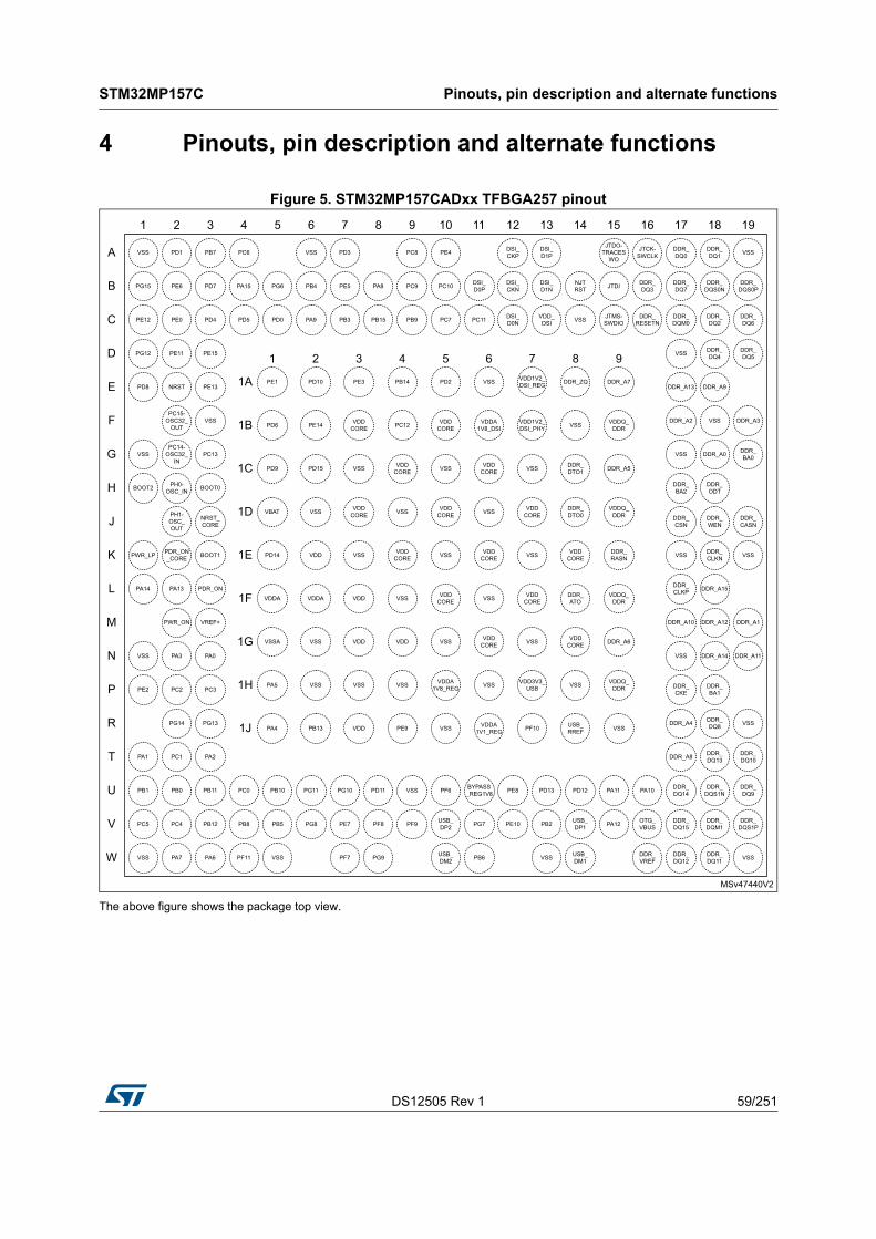
DS12505 Rev 1 59/251
STM32MP157C Pinouts, pin description and alternate functions
123
4 Pinouts, pin description and alternate functions
Figure 5. STM32MP157CADxx TFBGA257 pinout
The above figure shows the package top view.
MSv47440V2
PB7 PC6 VSS PD3 PC8 PE4 DSI_CKP
DSI_D1P
JTDO-TRACES
WO
JTCK-SWCLK VSSDDR_
DQ0DDR_DQ1
PD7 PA15 PG6 PB4 PE5 PA8 PC9 PC10 DSI_CKN
DSI_D1N
NJTRST
DSI_D0P JTDI DDR_
DQ3DDR_
DQS0PDDR_DQ7
DDR_DQS0N
PD4 PD5 PD0 PA9 PB3 PB15 PB9 PC7 DSI_D0N
VDD_DSI VSSPC11 JTMS-
SWDIODDR_
RESETNDDR_DQ6
DDR_DQM0
DDR_DQ2
DDR_A7
VDDQ_DDR
DDR_A5
VDDQ_DDR
DDR_RASN
VDDQ_DDR
DDR_A6
VSS
PE15 DDR_DQ5
DDR_DQ4VSS
PE13 DDR_A9DDR_A13
VSS DDR_A3VSSDDR_A2
PC13 DDR_BA0DDR_A0VSS
BOOT0 DDR_ODT
DDR_BA2
NRST_CORE
DDR_CASN
DDR_WEN
DDR_CSN
BOOT1 VSSDDR_CLKNVSS
PDR_ON DDR_A15DDR_CLKP
VREF+ DDR_A1DDR_A12DDR_A10
PA0 DDR_A11DDR_A14VSS
PC3 DDR_BA1
DDR_CKE
PG13 VSSDDR_DQ8DDR_A4
PA2 DDR_DQ10
DDR_DQ13DDR_A8
PB11 PC0 PB10 PG11 PG10 PD11 VSS PF6 PE8 PD13 PD12BYPASS_REG1V8 PA11 PA10 DDR_
DQ9DDR_DQ14
DDR_DQS1N
PB12 PB8 PB5 PG8 PE7 PF8 PF9 USB_DP2 PE10 PB2 USB_
DP1PG7 PA12 OTG_VBUS
DDR_DQS1P
DDR_DQ15
DDR_DQM1
PA6 PF11 VSS PF7 PG9 USB_DM2 VSS USB_
DM1PB6 DDR_VREF VSSDDR_
DQ12DDR_DQ11
VSS
PG15
PE12
PG12
PD8
VSS
BOOT2
PWR_LP
PA14
VSS
PE2
PA1
PB1
PC5
VSS
PD1
PE6
PE0
PE11
NRST
PC15-OSC32_
OUT
PC14-OSC32_
IN
PH0-OSC_IN
PH1-OSC_OUT
PDR_ON_CORE
PA13
PWR_ON
PA3
PC2
PG14
PC1
PB0
PC4
PA7
DDR_ZQVDD1V2_DSI_REGVSSPD2PB14PE3PD10PE1
VSSVDD1V2_DSI_PHY
VDDA1V8_DSI
VDDCOREPC12VDD
COREPE14PD6
DDR_DTO1VSSVDD
COREVSSVDDCOREVSSPD15PD9
DDR_DTO0
VDDCOREVSSVDD
COREVSSVDDCOREVSSVBAT
VDDCOREVSSVDD
COREVSSVDDCOREVSSVDDPD14
DDR_ATO
VDDCOREVSSVDD
COREVSSVDDVDDAVDDA
VDDCOREVSSVDD
COREVSSVDDVDDVSSVSSA
VSSVDD3V3_USBVSSVDDA
1V8_REGVSSVSSVSSPA5
USB_RREFPF10VDDA
1V1_REGVSSPE9VDDPB13PA4
1 92 3 4 5 6 7 8
VDDQ_DDR
1A
1B
1C
1D
1E
1F
1G
1H
1J
191 3 1817121110987654 161514132
A
B
C
D
E
F
G
H
J
K
L
M
N
P
R
T
U
V
W

Pinouts, pin description and alternate functions STM32MP157C
60/251 DS12505 Rev 1
Figure 6. STM32MP157CABxx LFBGA354 pinout
The above figure shows the package top view.
MSv47439V2
VSSPE9 PF7 PF9 PG7 VDDA1V1_REG
VDD3V3_USBHS
USB_DP2VSS PA2 PB0 PC4 PB10 PB8 DDR_
DQ12DDR_DQ15
DDR_VREF
VDD3V3_USBFS
USB_DM1
A
B
C
D
E
F
G
H
J
K
L
M
N
P
R
T
U
V
W
VSS
PE1
PE11
VSS
PE15
PG12
PD15
PC14-OSC32_
IN
NRST
BOOT0
PWR_ON
PH0-OSC_IN
PDR_ON_CORE
PWR_LP
PA14
PE2
PG14
PB11
PG15
VSS
PE13
PE12
VSS
PD8
VSS
PC15-OSC32_
OUT
NRST_CORE
VSS
BOOT2
PH1-OSC_OUT
PDR_ON
PA13
VSS
PC2
PG13
PC1
PD0
PE6
VSS
PE14
PD6
PD14
PD9
VBAT
VSS
PC13
VDD_ANA
VREF-
VREF+
PA3
PA0
PC3
VSS
PB1
PD1
PD7
PE0
VSS
VSS
VDDCORE
VSS
VDDCORE
VSS_PLL
BOOT1
VSS_ANA
VDDA
VSSA
PA5
PA4
VSS
PA1
PC5
PE3
PB7
PD10
VSS
VSS
VSS
VDDCORE
VSS
VDD_PLL
VSS
VDD
VSS
VDD
VSSA
VSSA
PA6
PF11
PB12
PG6
VSS
PD3
PD4
VSS
VDDCORE
VSS
VDDCORE
VSS
VDD
VSS
VDD
VSS
VDD
VSS
PA7
VSS
PG11
PB3
PE5
PA15
PD5
VDDCORE
VSS
VDDCORE
VSS
VDDCORE
VSS
VDD
VSS
VDD
VSS
VDD
PC0
PG8
PG10
PB15
PA8
PA9
VSS
VSS
VDDCORE
VSS
VDDCORE
VSS
VDDCORE
VSS
VDD
VSS
VDD
VSS
PB5
VSS
PD11
PC7
PB4
PB14
PB9
VDDCORE
VSS
VDDCORE
VSS
VDDCORE
VSS
VDDCORE
VSS
VDD
VSS
VDD
PB13
PF10
PF6
PC9
PD2
PC12
PC6
VSS
VDDCORE
VSS
VDDCORE
VSS
VDDCORE
VSS
VDDCORE
VSS
VDD
VSS
PE7
PF8
PE10
PC11
PE4
PC8
PC10
VDDCORE
VSS
VDDCORE
VSS
VDDCORE
VSS
VDDCORE
VSS
VDDCORE
VSS
VDD
PE8
PD12
VDDA1V8_REG
VDD_DSI
VDDA1V8_DSI
VSS_DSI
NJTRST
VSS
VDDCORE
VSS
VDDCORE
VSS
VDDCORE
VSS
VDDCORE
VSS
VDDCORE
VSS
PB6
PD13
VSS_USBHS
DSI_D0N
DSI_D0P
VSS_DSI
JTDI
VDDCORE
VSS_PLL2
VDD_PLL2
VSS
VDDCORE
VSS
VDDCORE
VSS
VDDCORE
VSS
VDDCORE
PB2
VSS_USBHS
USB_DM2
DSI_CKN
DSI_CKP
VSS_DSI
JTDO-TRACESWO
VSS
VDDQ_DDR
VSS
VDDQ_DDR
VSS
VDDQ_DDR
VSS
VDDQ_DDR
VSS
VDDQ_DDR
VSS
PG9
VSS_USBHS
USB_DP1
DSI_D1N
DSI_D1P
VSS_DSI
JTMS-SWDIO
VDDQ_DDR
VSS
VDDQ_DDR
VSS
VDDQ_DDR
VSS
VDDQ_DDR
VSS
VDDQ_DDR
VSS
VDDQ_DDR
BYPASS_REG1V8
OTG_VBUS
VSS_USBHS
VDD1V2_DSI_PHY
VDD1V2_DSI
_REG
VSS_DSI
JTCK-SWCLK
VSS
DDR_RESETN
DDR_BA2
DDR_A15
DDR_A6
VSS
PA10
PA12
USB_RREF
DDR_DQ0
DDR_DQ3
VSS
DDR_DQ5
DDR_A7
DDR_A13
DDR_A9
DDR_A5
DDR_WEN
DDR_CASN
DDR_A12
DDR_A1
DDR_BA1
DDR_A4
DDR_A8
DDR_DQ9
VSS
PA11
DDR_DQ1
DDR_DQ7
DDR_DQM0
DDR_DQ2
DDR_DQ4
DDR_ZQ
DDR_A2
DDR_A0
DDR_CSN
DDR_DTO0
DDR_RASN
DDR_A11
DDR_A14
DDR_DQ8
DDR_DQ10
DDR_DQ13
DDR_DQM1
DDR_DQ14
DDR_DQS0N
DDR_DQS0P
DDR_DQ6
VSS
DDR_A3
DDR_BA0
DDR_ODT
DDR_CLKN
DDR_CLKP
DDR_A10
DDR_DTO1
DDR_CKE
DDR_DQS1N
DDR_ATO
DDR_DQ11
DDR_DQS1P
191 43 141312111098765 181716152

DS12505 Rev 1 61/251
STM32MP157C Pinouts, pin description and alternate functions
123
Figure 7. STM32MP157CACxx TFBGA361 pinout
The above figure shows the package top view.
MSv47430V3
PH15 PH12 PH4 PE12 PD10 PD4 PG15 PD0 PD1 PB9 PC7 PB15 PC6 DSI_D0N
DSI_CKPPB4 DSI_
D1PVDD_DSI
NJTRST
PI0 PH10 PH14 PH11 PH9 PE14 VSS PE1 PE3 PE6 PE5 VSS VDDA1V8_DSI
DSI_D0P
VSS_DSIPB14
VDD1V2_DSI_PHY
VDD1V2_DSI_REG
PA15
PH13 PD6 PE15 VSS PH8 PE0 PF5 PF0 PF4 PD7 PB7 PD2 PD3 PC10 PC11PC12 PC9 PC8 PE4
VSS PH5 PE13 PE11 PF1 PD5 PA9 PG6 PB3 PF2 DSI_CKNPA8 DSI_
D1N
JTDO-TRACESWO
VSS PG0 PA2 PF14 PB12 PC4 PA6 VSSPD11 PF8 PG7 USB_DP2PE8 USB_
DP1OTG_VBUS
DDR_VREF
DDR_DQ29
DDR_DQ28
PE2 PC2 PB10
PA4
PF13 PG5 PG11 PB5 DDR_DQ24PF12 PF11 PH6 PF10 PB6 PE10 PB2PG9 PA10 PD12 DDR_
ATODDR_
A8DDR_DQ15
DDR_DQ25
PG14 PG13 PH3 PA1 VSS PC1 PB1 VSS DDR_DQ30PE9 PB13 PE7 VSS PF9
VDD3V3_
USBHS
VSS_USBHSPF6
VDD3V3_
USBFSPA11 PD13 DDR_
DQM3 VSS DDR_DQ31
PB11 PG4 PA0 PH2 PC0 PB0 PC5 PA7 DDR_DQS3NPG8 PB8 PG10 PF7
VDDA1V8_REG
VDDA1V1_REG
USB_DM2
BYPASS_REG
1V8
USB_DM1
USB_RREF PA12 DDR_
DQ27DDR_DQ26
DDR_DQS3P
DDR_DQ12
DDR_DQ14
DDR_DQ11
DDR_A6
DDR_DQ13
DDR_DQ10
DDR_DQ8
DDR_CKE
DDR_DQS1N
DDR_DQS1P
DDR_DQ9
DDR_BA1
DDR_DQM1VSSDDR_
A4
DDR_A10
DDR_A14
DDR_A11
DDR_CSN
DDR_BA2
DDR_WEN
DDR_CLKN
DDR_CLKP
DDR_RASN
DDR_CASN
DDR_A12
DDR_A1VSSDDR_
A15
DDR_BA0
DDR_ODT
DDR_TO1
DDR_A0
DDR_DQM0
DDR_DQ6
DDR_DQ2
DDR_A5
DDR_DQ5
DDR_DQ4
DDR_A2
DDR_ZQ
DDR_A3VSSDDR_
DTO0
DDR_DQ21
DDR_DQ0
DDR_DQ3
DDR_A7
DDR_DQ1VSSDDR_
A13
DDR_DQS0N
DDR_DQS0P
DDR_DQ7
DDR_A9
PG1 PC3 VSS PH7
PI10 PA14PDR_ON_
COREPG3
PF3 PA3 ANA0 ANA1
PG2 PA5
PF15
PWR_ON
PDR_ON VREF+
BOOT2 NRST NRST_CORE
BOOT0 PA13 PWR_LP BOOT1
PH0-OSC_IN
PH1-OSC_OUT
VSS PI11
PC15-OSC32_OUT
PC14-OSC32
_INPD14 PI8
PZ6 PZ5 VSS PI9
PD15 PZ7 PZ2
PD9 PC13 PD8 PG12
PI3 PI2 PI1 PI4
PI7 PI5 PI6
PZ1 PZ4 PZ0 PZ3
DDR_DQS2N
JTCK-SWCLK
DDR_DQ19
DDR_DQ16
DDR_DQM2
JTMS-SWDIO VSS DDR_
DQS2P
DDR_DQ18
DDR_RESET
N
DDR_DQ22
DDR_DQ17
VSSJTDI DDR_DQ20
DDR_DQ23
VDDCORE
VSS
VDDCORE
VSS
VBAT
VSS_ANA
VDDA
VDDCORE
VSS
VDDCORE
VSS
VDDCORE
VSS
VDD_ANA
VSSA
VDD
VSS
VDDCORE
VSS
VDDCORE
VSS
VDD
VSS
VDD
VSS
VDDCORE
VSS
VDDCORE
VSS
VDDCORE
VSS
VDD
VSS
VDD
VSS
VDDCORE
VSS
VDDCORE
VSS
VDDCORE
VSS
VDD
VSS
VDDCORE
VSS
VDDCORE
VSS
VDDCORE
VSS
VDDCORE
VSS
VDD
VSS
VDDQ_DDR
VSS
VDDCORE
VSS
VDDCORE
VSS
VDDCORE
VSS
VDDQ_DDR
VSS
VDDQ_DDR
VSS
VDDQ_DDR
VSS
VDDQ_DDR
VSS
VDDQ_DDR
VDDQ_DDR
VSS
VDDQ_DDR
VSS
VDDQ_DDR
VSS
VDDQ_DDR
1 92 3 4 5 6 7 8
1A
1B
1C
1D
1E
1F
1G
1H
1J
A
B
C
D
E
F
G
H
J
K
L
M
N
P
R
T
U
V
W
Y
AA
AB
AC
231 43 222120141312111098765 19181716152

Pinouts, pin description and alternate functions STM32MP157C
62/251 DS12505 Rev 1
Figure 8. STM32MP157CAA LFBGA448 pinout
The above figure shows the package top view.
MSv47431V3
A
B
C
D
E
F
G
H
J
K
L
M
N
P
R
T
U
V
W
Y
AA
AB
PH10 VSS PH11 PE14 PK7 PK3 PJ14 PJ12 PF1 PD1 PD3 PB15VDDA1V8_DSI
DSI_D0P
DSI_CKPPA8 DSI_
D1P
VDD1V2_DSI_
REGVSS DDR_
DQS2NDDR_DQ19
DDR_DQ16
PH15 PH14 VSS PE15 PE0 PK5 PJ15 VSS PD4 PD0 VSS PE5 VSS_DSI
VSS_DSI
VSS_DSIPB4 VSS_
DSIVSS_DSI VSS DDR_
DQM2VSS DDR_DQS2P
PI0 PI14 PH13 VSS PE11 PH8 PE1 PK0 PF5 PG15 PG6 PD2 PC9 PC11 JTDIPC7 JTCK-SWCLK
VDD_PLL2
VSS_PLL2
DDR_DQ18
DDR_DQ22
DDR_DQ17
VSS PH5 PH4 PE13 PK6 PK4 PJ13 PD10 PD5 PE3 PA9 PB3 VDD_DSI
DSI_D0N
DSI_CKNPB14 DSI_
D1N
VDD1V2_DSI_PHY
VSS VSSDDR_DQ20
DDR_DQ23
PI7 PI5 PI15 PZ3 PH12 VSS VSS VSS PF4 PD7 PB7 PB9 PC10 PE4 VSSPF2 VDDQ_DDR
DDR_A7
DDR_RESET
NVSS DDR_
DQ1
PZ4 PZ0 PZ6 VSS PI6 VSS VSS VSS VSS VSS VDDQ_DDR VSS DDR_
A13DDR_DQ7
DDR_DQS0P
DDR_DQM0
DDR_DQS0N
PI13 PI12 PZ7 PZ5 PZ1 PJ8 VSS VDDCORE
VDDCORE
VDDCORE
VDDCORE
VDDQ_DDR
DDR_A9
DDR_A5
DDR_DQ6
DDR_DQ5
DDR_DQ2
PI2 PI1 PI3 PE12 VSS PH9 PK1 PK2 PE6 PF0 PA15 PC12 PC8 NJTRST
JTDO-TRACESWO
PC6 JTMS-SWDIO
VDDQ_DDR VSS DDR_
DQ21DDR_DQ3
DDR_DQ0
PJ5 PJ4 VSS PJ2 PZ2 PJ11 VSS VDDCORE VSS VDD
CORE VSS VSS VDDCORE
VDDCORE
VDDQ_DDR
DDR_BA2
DDR_A0
DDR_ZQ
DDR_BA0
DDR_DTO1
PD15 PJ9 PD6 PJ7 PJ6 PJ1 VDDCORE VSS VDD
CORE VSS VDDCORE
VDDCORE
VDDQ_DDRVSS VSS DDR_
CSN VSS DDR_DTO0VSS DDR_
ODT
PD8 PD9 PD14 VBAT VSS_PLL
VDD_PLL VSS VDD VSS VDD
CORE VSS VSS VDDCORE
VDDCORE
VDDQ_DDR
DDR_A1
DDR_A15
DDR_CASN
DDR_RASN
DDR_WEN
PJ3 PJ0 PJ10 PG12 PI9 PI4 VDDCORE VSS VDD
CORE VSS VDDCORE
VDDCORE
VDDQ_DDRVSS VSS DDR_
A2DDR_
A3 VSS DDR_DQ4
PC14-OSC32
_IN
PC15-OSC32_OUT
VSS BOOT2 VSS_ANA VREF+ VSS VDD VSS VDD VSS VSS VDD
COREVDD
COREVDDQ_
DDRDDR_A14
DDR_A11 VSS DDR_
DQ10
NRST_CORE NRST PA14 ANA0 VDDA VSSA VSS VDD VDD VDD
COREVDDQ_
DDR VSS DDR_BA1
DDR_CKE
DDR_DQS1N
DDR_DQ13
DDR_DQ9
PH0-OSC_IN
PH1-OSC_OUT
PI11 PA3 ANA1 VSSA VSS VSS VSS VDDCOREVDD VDDQ_
DDRDDR_
A4 VSS DDR_DQS1P
DDR_DQ11
DDR_DQM1
PI8 PC13 BOOT0 BOOT1 VDD_ANA VREF- VDD VSS VDD VSS VDD
COREVDD
COREVDDQ_
DDRVSS VSS DDR_A10
DDR_A12
DDR_DQ8
DDR_CLKP
DDR_CLKN
PWR_ON
PDR_ON PF3 PA1 VSS PA4 PF14 PF12 PB10 PB13 PH6 PF10 PD13 OTG_
VBUS VSSPB2 VDDQ_DDR VSS VSS DDR_
DQ24DDR_DQ12
DDR_DQ15
PI10 PH7 PA13 PG2 PG0 PF15 PF13 PF11 PA6 PE7 PE9 PD12 PE10 PG9 PA12PB6 VSS VDDQ_DDR VSS DDR_
DQ30DDR_DQ25
DDR_DQ31
PC2 PE2 VSS PG1 PB11 PH3 VSS PG8 PA7 VSS PG7 PE8 VSS_USBHS
VSS_USBHS PA11VSS_
USBHS PA10 VSS VDDQ_DDR
DDR_DQS3NVSS DDR_
DQS3P
PWR_LP
PDR_ON_
COREPC3 PG3 PA5 VSSA VSS PG5 VDD PC0 PG11 VDD VDD VSS VDDQ_
DDRVSS VSS DDR_A8
DDR_A6 VSS DDR_
DQ14
VSS PA2 PC1 PG4 PB0 PC4 PH2 PB8 PD11 PF8 PF9VDDA1V8_REG
USB_DP2
USB_DM1
VDD3V3_
USBFS
VDD3V3_
USBHS
VDDA1V1_REG
VSS DDR_VREF VSSDDR_
DQ27DDR_DQ26
PG13 PG14 PA0 VSS PB1 PC5 PB12 PB5 PG10 PF7 PF6BYPASS_REG
1V8
USB_DM2
USB_DP1
VSS_USBHS
VSS_USBHS
USB_RREF VSS DDR_
ATODDR_DQM3
DDR_DQ29
DDR_DQ28
221 43 2120141312111098765 19181716152

DS12505 Rev 1 63/251
STM32MP157C Pinouts, pin description and alternate functions
123
Table 6. Legend/abbreviations used in the pinout table
Name Abbreviation Definition
Pin nameUnless otherwise specified, the pin function during and after reset is the same as the actual pin name
Pin type
S Supply pin
I Input only pin
O Output only pin
I/O Input / output pin
A Analog or special level pin
I/O structure
FT(U/D/PD) 5 V tolerant I/O (with fixed pull-up / pull-down / programmable pull-down)
TT 3.6 V tolerant I/O directly connected to DAC
DDR 1.5 V, 1.35 V or 1.2 V I/O for DDR3, DDR3L, LPDDR2/LPDDR3 interface
DSI 1.2 V I/O for DSI interface
A Analog signal
RST Reset pin with weak pull-up resistor
Option for TT or FT I/Os
_f(1) I2C FM+ option
_a(2) Analog option (supplied by VDDA for the analog part of the I/O)
_u(3) USB option (supplied by VDD3V3_USBxx for the USB part of the I/O)
_h(4) High-speed output for 1.8V typ. VDD (for SPI, SDMMC, QUADSPI, TRACE)
_e(5) Very-high-speed option for 1.8V typ. VDD (for ETH, SPI, SDMMC, QUADSPI, TRACE)
Notes Unless otherwise specified by a note, all I/Os are set as floating inputs during and after reset
Alternate functions
Functions selected through GPIOx_AFR registers
Additional functions
Functions directly selected/enabled through peripheral registers
1. The related I/O structures in Table 7 are: FT_f, FT_fae, FT_fh, FT_fha, FT_uf
2. The related I/O structures in Table 7 are: FT_a, TT_a, FT_ae, FT_fae, FT_fha, FT_ha, TT_ha
3. The related I/O structures in Table 7 are: FT_u, FT_uf
4. The related I/O structures in Table 7 are: FT_h, FT_fh, FT_fha, FT_ha, TT_ha
5. The related I/O structures in Table 7 are: FT_e, FT_ae, FT_fae
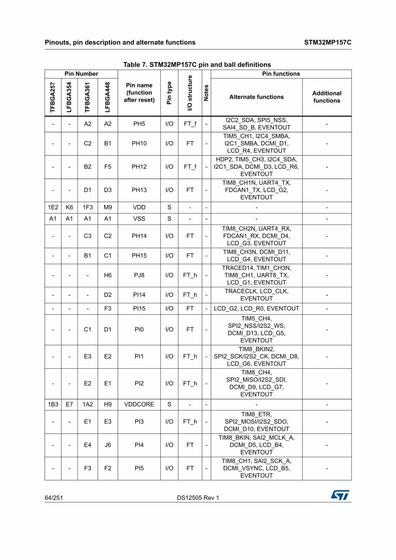
Pinouts, pin description and alternate functions STM32MP157C
64/251 DS12505 Rev 1
Table 7. STM32MP157C pin and ball definitions Pin Number
Pin name (function
after reset) Pin
typ
e
I/O s
tru
ctu
re
No
tes
Pin functions
TF
BG
A25
7
LF
BG
A35
4
TF
BG
A36
1
LF
BG
A44
8
Alternate functionsAdditional functions
- - A2 A2 PH5 I/O FT_f -I2C2_SDA, SPI5_NSS,
SAI4_SD_B, EVENTOUT-
- - C2 B1 PH10 I/O FT -TIM5_CH1, I2C4_SMBA, I2C1_SMBA, DCMI_D1, LCD_R4, EVENTOUT
-
- - B2 F5 PH12 I/O FT_f -HDP2, TIM5_CH3, I2C4_SDA,
I2C1_SDA, DCMI_D3, LCD_R6, EVENTOUT
-
- - D1 D3 PH13 I/O FT -TIM8_CH1N, UART4_TX, FDCAN1_TX, LCD_G2,
EVENTOUT-
1E2 K6 1F3 M9 VDD S - - - -
A1 A1 A1 A1 VSS S - - - -
- - C3 C2 PH14 I/O FT -TIM8_CH2N, UART4_RX, FDCAN1_RX, DCMI_D4,
LCD_G3, EVENTOUT-
- - B1 C1 PH15 I/O FT -TIM8_CH3N, DCMI_D11,
LCD_G4, EVENTOUT-
- - - H6 PJ8 I/O FT_h -TRACED14, TIM1_CH3N, TIM8_CH1, UART8_TX, LCD_G1, EVENTOUT
-
- - - D2 PI14 I/O FT_h -TRACECLK, LCD_CLK,
EVENTOUT-
- - - F3 PI15 I/O FT - LCD_G2, LCD_R0, EVENTOUT -
- - C1 D1 PI0 I/O FT -
TIM5_CH4, SPI2_NSS/I2S2_WS, DCMI_D13, LCD_G5,
EVENTOUT
-
- - E3 E2 PI1 I/O FT_h -TIM8_BKIN2,
SPI2_SCK/I2S2_CK, DCMI_D8, LCD_G6, EVENTOUT
-
- - E2 E1 PI2 I/O FT_h -
TIM8_CH4, SPI2_MISO/I2S2_SDI, DCMI_D9, LCD_G7,
EVENTOUT
-
1B3 E7 1A2 H9 VDDCORE S - - - -
- - E1 E3 PI3 I/O FT_h -TIM8_ETR,
SPI2_MOSI/I2S2_SDO, DCMI_D10, EVENTOUT
-
- - E4 J6 PI4 I/O FT -TIM8_BKIN, SAI2_MCLK_A,
DCMI_D5, LCD_B4, EVENTOUT
-
- - F3 F2 PI5 I/O FT -TIM8_CH1, SAI2_SCK_A, DCMI_VSYNC, LCD_B5,
EVENTOUT-
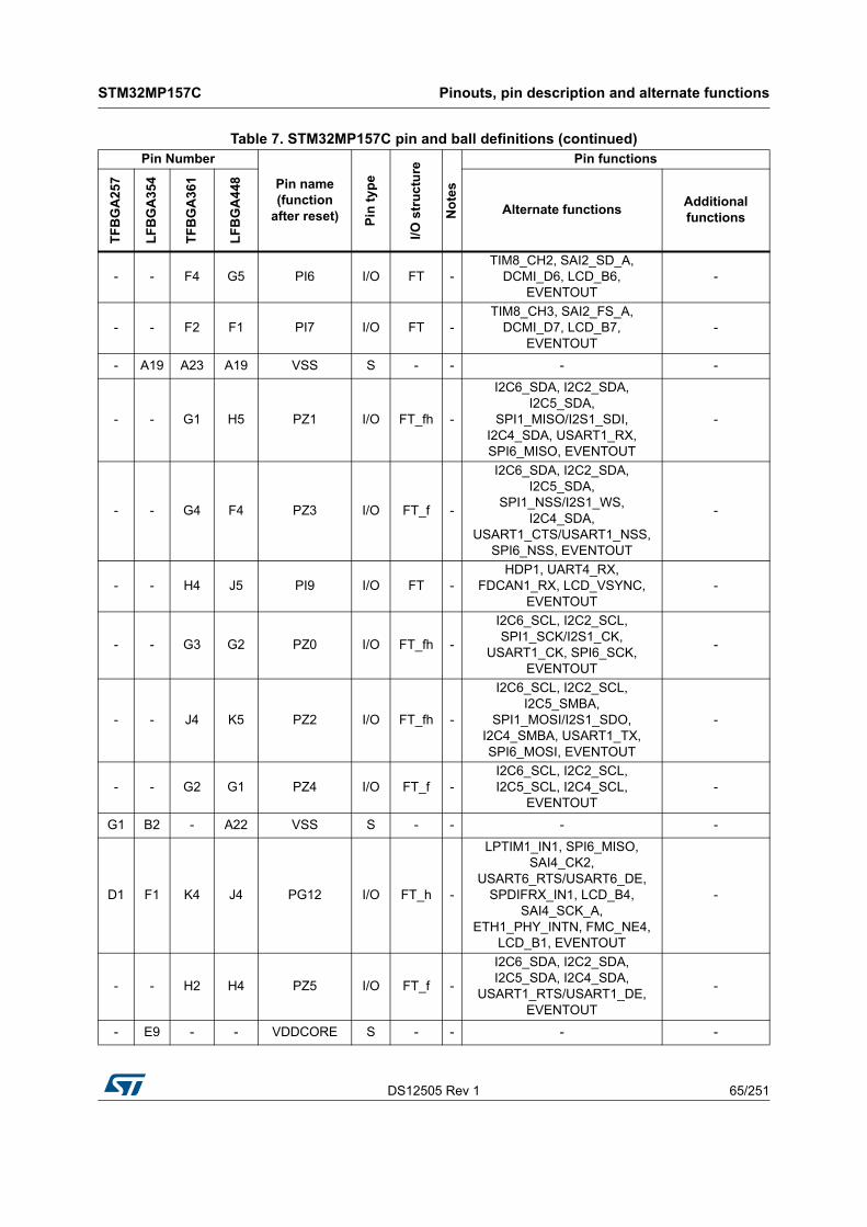
DS12505 Rev 1 65/251
STM32MP157C Pinouts, pin description and alternate functions
123
- - F4 G5 PI6 I/O FT -TIM8_CH2, SAI2_SD_A,
DCMI_D6, LCD_B6, EVENTOUT
-
- - F2 F1 PI7 I/O FT -TIM8_CH3, SAI2_FS_A,
DCMI_D7, LCD_B7, EVENTOUT
-
- A19 A23 A19 VSS S - - - -
- - G1 H5 PZ1 I/O FT_fh -
I2C6_SDA, I2C2_SDA, I2C5_SDA,
SPI1_MISO/I2S1_SDI, I2C4_SDA, USART1_RX, SPI6_MISO, EVENTOUT
-
- - G4 F4 PZ3 I/O FT_f -
I2C6_SDA, I2C2_SDA, I2C5_SDA,
SPI1_NSS/I2S1_WS, I2C4_SDA,
USART1_CTS/USART1_NSS, SPI6_NSS, EVENTOUT
-
- - H4 J5 PI9 I/O FT -HDP1, UART4_RX,
FDCAN1_RX, LCD_VSYNC, EVENTOUT
-
- - G3 G2 PZ0 I/O FT_fh -
I2C6_SCL, I2C2_SCL, SPI1_SCK/I2S1_CK,
USART1_CK, SPI6_SCK, EVENTOUT
-
- - J4 K5 PZ2 I/O FT_fh -
I2C6_SCL, I2C2_SCL, I2C5_SMBA,
SPI1_MOSI/I2S1_SDO, I2C4_SMBA, USART1_TX, SPI6_MOSI, EVENTOUT
-
- - G2 G1 PZ4 I/O FT_f -I2C6_SCL, I2C2_SCL, I2C5_SCL, I2C4_SCL,
EVENTOUT-
G1 B2 - A22 VSS S - - - -
D1 F1 K4 J4 PG12 I/O FT_h -
LPTIM1_IN1, SPI6_MISO, SAI4_CK2,
USART6_RTS/USART6_DE, SPDIFRX_IN1, LCD_B4,
SAI4_SCK_A, ETH1_PHY_INTN, FMC_NE4,
LCD_B1, EVENTOUT
-
- - H2 H4 PZ5 I/O FT_f -
I2C6_SDA, I2C2_SDA, I2C5_SDA, I2C4_SDA,
USART1_RTS/USART1_DE, EVENTOUT
-
- E9 - - VDDCORE S - - - -
Table 7. STM32MP157C pin and ball definitions (continued)Pin Number
Pin name (function
after reset) Pin
ty
pe
I/O s
tru
ctu
re
No
tes
Pin functions
TF
BG
A25
7
LF
BG
A35
4
TF
BG
A36
1
LF
BG
A44
8
Alternate functionsAdditional functions

Pinouts, pin description and alternate functions STM32MP157C
66/251 DS12505 Rev 1
- - H1 G3 PZ6 I/O FT_f -
I2C6_SCL, I2C2_SCL, USART1_CK, I2S1_MCK,
I2C4_SMBA, USART1_RX, EVENTOUT
-
- - J3 H3 PZ7 I/O FT_f -I2C6_SDA, I2C2_SDA,
USART1_TX, EVENTOUT-
- - - H2 PI12 I/O FT_h -TRACED0, HDP0,
LCD_HSYNC, EVENTOUT-
- B6 C7 B2 VSS S - - - -
- - - H1 PI13 I/O FT_h -TRACED1, HDP1,
LCD_VSYNC, EVENTOUT-
- - 1A4 H11 VDDCORE S - - - -
- - - J3 PJ10 I/O FT_h -TIM1_CH2N, TIM8_CH2,
SPI5_MOSI, LCD_G3, EVENTOUT
-
- - - K6 PJ11 I/O FT_h -TIM1_CH2, TIM8_CH2N,
SPI5_MISO, LCD_G4, EVENTOUT
-
- - - J2 PJ0 I/O FT_h -TRACED8, LCD_R7, LCD_R1,
EVENTOUT-
- - - L6 PJ1 I/O FT_h -TRACED9, LCD_R2,
EVENTOUT-
- - - K4 PJ2 I/O FT_h -TRACED10, DSI_TE, LCD_R3,
EVENTOUT-
- L5 - - VDD S - - - -
- - - J1 PJ3 I/O FT_h -TRACED11, LCD_R4,
EVENTOUT-
N1 C3 - B19 VSS S - - - -
- - - K2 PJ4 I/O FT_h -TRACED12, LCD_R5,
EVENTOUT-
1D3 E11 - - VDDCORE S - - - -
- - - K1 PJ5 I/O FT_h -TRACED2, HDP2, LCD_R6,
EVENTOUT-
- - - L5 PJ6 I/O FT_h -TRACED3, HDP3, TIM8_CH2,
LCD_R7, EVENTOUT-
- - - L4 PJ7 I/O FT_h -TRACED13, TIM8_CH2N,
LCD_G0, EVENTOUT-
- C17 C12 C3 VSS S - - - -
Table 7. STM32MP157C pin and ball definitions (continued)Pin Number
Pin name (function
after reset) Pin
ty
pe
I/O s
tru
ctu
re
No
tes
Pin functions
TF
BG
A25
7
LF
BG
A35
4
TF
BG
A36
1
LF
BG
A44
8
Alternate functionsAdditional functions
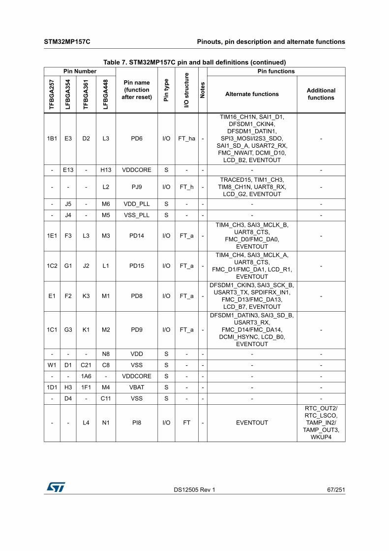
DS12505 Rev 1 67/251
STM32MP157C Pinouts, pin description and alternate functions
123
1B1 E3 D2 L3 PD6 I/O FT_ha -
TIM16_CH1N, SAI1_D1, DFSDM1_CKIN4, DFSDM1_DATIN1,
SPI3_MOSI/I2S3_SDO, SAI1_SD_A, USART2_RX, FMC_NWAIT, DCMI_D10,
LCD_B2, EVENTOUT
-
- E13 - H13 VDDCORE S - - - -
- - - L2 PJ9 I/O FT_h -TRACED15, TIM1_CH3,
TIM8_CH1N, UART8_RX, LCD_G2, EVENTOUT
-
- J5 - M6 VDD_PLL S - - - -
- J4 - M5 VSS_PLL S - - - -
1E1 F3 L3 M3 PD14 I/O FT_a -
TIM4_CH3, SAI3_MCLK_B, UART8_CTS,
FMC_D0/FMC_DA0, EVENTOUT
-
1C2 G1 J2 L1 PD15 I/O FT_a -
TIM4_CH4, SAI3_MCLK_A, UART8_CTS,
FMC_D1/FMC_DA1, LCD_R1, EVENTOUT
-
E1 F2 K3 M1 PD8 I/O FT_a -
DFSDM1_CKIN3, SAI3_SCK_B, USART3_TX, SPDIFRX_IN1,
FMC_D13/FMC_DA13, LCD_B7, EVENTOUT
-
1C1 G3 K1 M2 PD9 I/O FT_a -
DFSDM1_DATIN3, SAI3_SD_B, USART3_RX,
FMC_D14/FMC_DA14, DCMI_HSYNC, LCD_B0,
EVENTOUT
-
- - - N8 VDD S - - - -
W1 D1 C21 C8 VSS S - - - -
- - 1A6 - VDDCORE S - - - -
1D1 H3 1F1 M4 VBAT S - - - -
- D4 - C11 VSS S - - - -
- - L4 N1 PI8 I/O FT - EVENTOUT
RTC_OUT2/RTC_LSCO, TAMP_IN2/
TAMP_OUT3, WKUP4
Table 7. STM32MP157C pin and ball definitions (continued)Pin Number
Pin name (function
after reset) Pin
ty
pe
I/O s
tru
ctu
re
No
tes
Pin functions
TF
BG
A25
7
LF
BG
A35
4
TF
BG
A36
1
LF
BG
A44
8
Alternate functionsAdditional functions

Pinouts, pin description and alternate functions STM32MP157C
68/251 DS12505 Rev 1
G3 K3 K2 N2 PC13 I/O FT - EVENTOUT
RTC_OUT1/RTC_TS/
RTC_LSCO, TAMP_IN1/
TAMP_OUT2/TAMP_OUT3,
WKUP3
F3 D5 D4 C19 VSS S - - - -
F2 H2 L1 P2PC15-
OSC32_OUTI/O FT - EVENTOUT OSC32_OUT
- F4 - H15 VDDCORE S - - - -
1C4 F6 1B1 - VDDCORE S - - - -
G2 H1 L2 P1PC14-
OSC32_INI/O FT - EVENTOUT OSC32_IN
E2 J1 M3 R2 NRST I/O RST - - -
J3 J2 M4 R1 NRST_CORE I RST - - -
H3 K1 N1 N3 BOOT0 I FTPD - - -
K3 K4 N4 N4 BOOT1 I FTPD - - -
H1 L2 M2 P4 BOOT2 I FTPD - - -
H2 M1 P1 T1 PH0-OSC_IN I/O FT - EVENTOUT OSC_IN
- - - J8 VDDCORE S - - - -
J2 M2 P2 T2PH1-
OSC_OUTI/O FT - EVENTOUT OSC_OUT
- D8 - C20 VSS S - - - -
M2 L1 R2 V1 PWR_ON O FT - - PWR_ONLP
K1 P1 N3 U1 PWR_LP O FT - - -
K2 N1 T3 U2PDR_ON_
COREI FT - - -
L3 N2 R3 V2 PDR_ON I FT - - -
- L3 1G2 N5 VDD_ANA S - - - -
- L4 1G1 P5 VSS_ANA S - - - -
L2 P2 N2 W3 PA13 I/O FT_a -DBTRGO, DBTRGI, MCO1,
UART4_TX, EVENTOUTBOOTFAILN
L1 R1 T2 R3 PA14 I/O FT_a -DBTRGO, DBTRGI, MCO2,
EVENTOUT-
- - P4 T3 PI11 I/O FT -MCO1, I2S_CKIN, LCD_G6,
EVENTOUTWKUP5
Table 7. STM32MP157C pin and ball definitions (continued)Pin Number
Pin name (function
after reset) Pin
ty
pe
I/O s
tru
ctu
re
No
tes
Pin functions
TF
BG
A25
7
LF
BG
A35
4
TF
BG
A36
1
LF
BG
A44
8
Alternate functionsAdditional functions

DS12505 Rev 1 69/251
STM32MP157C Pinouts, pin description and alternate functions
123
- - T1 W1 PI10 I/O FT -
HDP0, USART3_CTS/USART3_NSS,
ETH1_GMII_RX_ER/ETH1_MII_RX_ER,
LCD_HSYNC, EVENTOUT
-
- L7 1G4 - VDD S - - - -
W5 E2 F21 - VSS S - - - -
- F8 - - VDDCORE S - - - -
1F1 M4 1H1 R5 VDDA S - - - -
1F2 - - - VDDA S - - - -
M3 N3 R4 P6 VREF+ S - - - -
1G1 N4 1H2 R6 VSSA S - - - -
- P5 - T6 VSSA S - - - -
- R5 - U6 VSSA S - - - -
- M3 - N6 VREF- S - - - -
- - W4 W2 PH7 I/O FT_fh -
I2C3_SCL, SPI5_MISO, ETH1_GMII_RXD3/ETH1_MII_RXD3/
ETH1_RGMII_RXD3, MDIOS_MDC, DCMI_D9,
EVENTOUT
-
- - U1 V3 PF3 I/O FT_e -ETH1_GMII_TX_ER/
ETH1_MII_TX_ER, FMC_A3, EVENTOUT
-
P3 T3 W2 U3 PC3 I/O FT_ha -
TRACECLK, DFSDM1_DATIN1, SPI2_MOSI/I2S2_SDO, ETH1_GMII_TX_CLK/ETH1_MII_TX_CLK,
EVENTOUT
ADC1_INP13, ADC1_INN12
- - T4 U4 PG3 I/O FT_e -
TRACED3, TIM8_BKIN2, DFSDM1_CKIN1,
ETH1_GMII_TXD7, FMC_A13, EVENTOUT
-
P1 T1 Y1 Y2 PE2 I/O FT_fae -
TRACECLK, SAI1_CK1, I2C4_SCL, SPI4_SCK,
SAI1_MCLK_A, QUADSPI_BK1_IO2, ETH1_GMII_TXD3/ETH1_MII_TXD3/
ETH1_RGMII_TXD3, FMC_A23, EVENTOUT
-
- - - N10 VDD S - - - -
Table 7. STM32MP157C pin and ball definitions (continued)Pin Number
Pin name (function
after reset) Pin
ty
pe
I/O s
tru
ctu
re
No
tes
Pin functions
TF
BG
A25
7
LF
BG
A35
4
TF
BG
A36
1
LF
BG
A44
8
Alternate functionsAdditional functions
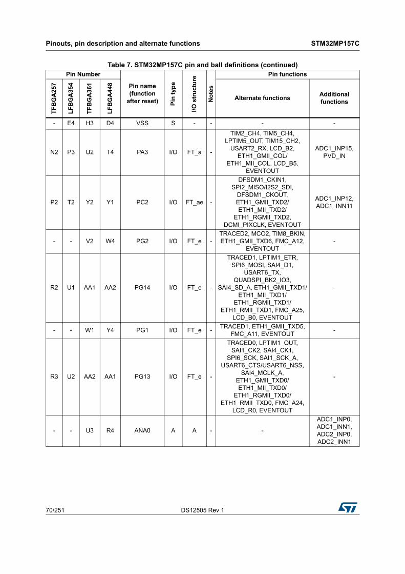
Pinouts, pin description and alternate functions STM32MP157C
70/251 DS12505 Rev 1
- E4 H3 D4 VSS S - - - -
N2 P3 U2 T4 PA3 I/O FT_a -
TIM2_CH4, TIM5_CH4, LPTIM5_OUT, TIM15_CH2,
USART2_RX, LCD_B2, ETH1_GMII_COL/
ETH1_MII_COL, LCD_B5, EVENTOUT
ADC1_INP15, PVD_IN
P2 T2 Y2 Y1 PC2 I/O FT_ae -
DFSDM1_CKIN1, SPI2_MISO/I2S2_SDI,
DFSDM1_CKOUT, ETH1_GMII_TXD2/ETH1_MII_TXD2/
ETH1_RGMII_TXD2, DCMI_PIXCLK, EVENTOUT
ADC1_INP12, ADC1_INN11
- - V2 W4 PG2 I/O FT_e -TRACED2, MCO2, TIM8_BKIN, ETH1_GMII_TXD6, FMC_A12,
EVENTOUT-
R2 U1 AA1 AA2 PG14 I/O FT_e -
TRACED1, LPTIM1_ETR, SPI6_MOSI, SAI4_D1,
USART6_TX, QUADSPI_BK2_IO3,
SAI4_SD_A, ETH1_GMII_TXD1/ETH1_MII_TXD1/
ETH1_RGMII_TXD1/ETH1_RMII_TXD1, FMC_A25,
LCD_B0, EVENTOUT
-
- - W1 Y4 PG1 I/O FT_e -TRACED1, ETH1_GMII_TXD5,
FMC_A11, EVENTOUT-
R3 U2 AA2 AA1 PG13 I/O FT_e -
TRACED0, LPTIM1_OUT, SAI1_CK2, SAI4_CK1,
SPI6_SCK, SAI1_SCK_A, USART6_CTS/USART6_NSS,
SAI4_MCLK_A, ETH1_GMII_TXD0/ETH1_MII_TXD0/
ETH1_RGMII_TXD0/ETH1_RMII_TXD0, FMC_A24,
LCD_R0, EVENTOUT
-
- - U3 R4 ANA0 A A - -
ADC1_INP0, ADC1_INN1, ADC2_INP0, ADC2_INN1
Table 7. STM32MP157C pin and ball definitions (continued)Pin Number
Pin name (function
after reset) Pin
ty
pe
I/O s
tru
ctu
re
No
tes
Pin functions
TF
BG
A25
7
LF
BG
A35
4
TF
BG
A36
1
LF
BG
A44
8
Alternate functionsAdditional functions

DS12505 Rev 1 71/251
STM32MP157C Pinouts, pin description and alternate functions
123
N3 R3 AB3 AA3 PA0 I/O FT_ha -
TIM2_CH1/TIM2_ETR, TIM5_CH1, TIM8_ETR,
TIM15_BKIN, USART2_CTS/USART2_NSS, UART4_TX, SDMMC2_CMD,
SAI2_SD_B, ETH1_GMII_CRS/ETH1_MII_CRS, EVENTOUT
ADC1_INP16, WKUP1
- E5 - E5 VSS S - - - -
- - U4 T5 ANA1 A A - -ADC1_INP1, ADC2_INP1
T1 U4 AA4 V4 PA1 I/O FT_ha -
ETH_CLK, TIM2_CH2, TIM5_CH2, LPTIM3_OUT,
TIM15_CH1N, USART2_RTS/USART2_DE,
UART4_RX, QUADSPI_BK1_IO3,
SAI2_MCLK_B, ETH1_GMII_RX_CLK/ETH1_MII_RX_CLK/
ETH1_RGMII_RX_CLK/ETH1_RMII_REF_CLK, LCD_R2, EVENTOUT
ADC1_INP17, ADC1_INN16
1H1 P4 V3 U5 PA5 I/O TT_ha -
TIM2_CH1/TIM2_ETR, TIM8_CH1N, SAI4_CK1,
SPI1_SCK/I2S1_CK, SPI6_SCK, SAI4_MCLK_A,
LCD_R4, EVENTOUT
ADC1_INP19, ADC1_INN18, ADC2_INP19, ADC2_INN18, DAC_OUT2
1J1 R4 V4 V6 PA4 I/O TT_a -
HDP0, TIM5_ETR, SAI4_D2, SPI1_NSS/I2S1_WS, SPI3_NSS/I2S3_WS,
USART2_CK, SPI6_NSS, SAI4_FS_A, DCMI_HSYNC, LCD_VSYNC, EVENTOUT
ADC1_INP18, ADC2_INP18, DAC_OUT1
- - AC2 W5 PG0 I/O FT_e -TRACED0, DFSDM1_DATIN0, ETH1_GMII_TXD4, FMC_A10,
EVENTOUT-
U3 V1 AB1 Y5 PB11 I/O FT_fae -
TIM2_CH4, LPTIM2_ETR, I2C2_SDA, DFSDM1_CKIN7,
USART3_RX, ETH1_GMII_TX_EN/ETH1_MII_TX_EN/
ETH1_RGMII_TX_CTL/ETH1_RMII_TX_EN, DSI_TE,
LCD_G5, EVENTOUT
-
Table 7. STM32MP157C pin and ball definitions (continued)Pin Number
Pin name (function
after reset) Pin
ty
pe
I/O s
tru
ctu
re
No
tes
Pin functions
TF
BG
A25
7
LF
BG
A35
4
TF
BG
A36
1
LF
BG
A44
8
Alternate functionsAdditional functions

Pinouts, pin description and alternate functions STM32MP157C
72/251 DS12505 Rev 1
- - AB2 AB4 PG4 I/O FT_e -
TIM1_BKIN2, ETH1_GMII_GTX_CLK/
ETH1_RGMII_GTX_CLK, FMC_A14, EVENTOUT
-
T3 W2 AC3 AB2 PA2 I/O FT_ha -
TIM2_CH3, TIM5_CH3, LPTIM4_OUT, TIM15_CH1, USART2_TX, SAI2_SCK_B,
SDMMC2_D0DIR, ETH1_MDIO, MDIOS_MDIO, LCD_R1,
EVENTOUT
ADC1_INP14, WKUP2
1F3 M6 - - VDD S - - - -
T2 V2 AA6 AB3 PC1 I/O FT_ha -
TRACED0, SAI1_D1, DFSDM1_DATIN0, DFSDM1_CKIN4,
SPI2_MOSI/I2S2_SDO, SAI1_SD_A, SDMMC2_CK, ETH1_MDC, MDIOS_MDC,
EVENTOUT
ADC1_INP11, ADC1_INN10, ADC2_INP11, ADC2_INN10,
TAMP_IN3, WKUP6
A6 - K21 E19 VSS S - - - -
- - Y6 U8 PG5 I/O FT -
TIM1_ETR, ETH1_GMII_CLK125/
ETH1_RGMII_CLK125, FMC_A15, EVENTOUT
-
- F10 1B3 J10 VDDCORE S - - - -
- - AA3 Y6 PH3 I/O FT_h -
DFSDM1_CKIN4, QUADSPI_BK2_IO1,
SAI2_MCLK_B, ETH1_GMII_COL/
ETH1_MII_COL, LCD_R1, EVENTOUT
-
U2 W3 AB6 AB5 PB0 I/O FT_a -
TIM1_CH2N, TIM3_CH3, TIM8_CH2N, DFSDM1_CKOUT,
UART4_CTS, LCD_R3, ETH1_GMII_RXD2/ETH1_MII_RXD2/
ETH1_RGMII_RXD2, MDIOS_MDIO, LCD_G1,
EVENTOUT
ADC1_INP9, ADC1_INN5, ADC2_INP9, ADC2_INN5
- - Y4 W6 PF15 I/O FT_fh -TRACED7, I2C4_SDA,
I2C1_SDA, ETH1_GMII_RXD7, FMC_A9, EVENTOUT
-
Table 7. STM32MP157C pin and ball definitions (continued)Pin Number
Pin name (function
after reset) Pin
ty
pe
I/O s
tru
ctu
re
No
tes
Pin functions
TF
BG
A25
7
LF
BG
A35
4
TF
BG
A36
1
LF
BG
A44
8
Alternate functionsAdditional functions

DS12505 Rev 1 73/251
STM32MP157C Pinouts, pin description and alternate functions
123
U1 V3 AA7 AA5 PB1 I/O FT_a -
TIM1_CH3N, TIM3_CH4, TIM8_CH3N, DFSDM1_DATIN1,
LCD_R6, ETH1_GMII_RXD3/ETH1_MII_RXD3/
ETH1_RGMII_RXD3, MDIOS_MDC, LCD_G0,
EVENTOUT
ADC1_INP5, ADC2_INP5
- E6 - F6 VSS S - - - -
- - AC4 V7 PF14 I/O FT_fha -
TRACED6, DFSDM1_CKIN6, I2C4_SCL, I2C1_SCL,
ETH1_GMII_RXD6, FMC_A8, EVENTOUT
ADC2_INP6, ADC2_INN2
- - Y5 W7 PF13 I/O FT_ha -
TRACED5, DFSDM1_DATIN6, I2C4_SMBA, I2C1_SMBA,
DFSDM1_DATIN3, ETH1_GMII_RXD5, FMC_A7,
EVENTOUT
ADC2_INP2
- - AB4 AB7 PH2 I/O FT_h -
LPTIM1_IN2, QUADSPI_BK2_IO0,
SAI2_SCK_B, ETH1_GMII_CRS/
ETH1_MII_CRS, LCD_R0, EVENTOUT
-
V1 V4 AB7 AA6 PC5 I/O FT_a -
SAI1_D3, DFSDM1_DATIN2, SAI4_D4, SAI1_D4,
SPDIFRX_IN3, ETH1_GMII_RXD1/ETH1_MII_RXD1/
ETH1_RGMII_RXD1/ETH1_RMII_RXD1, SAI4_D3,
EVENTOUT
ADC1_INP8, ADC1_INN4, ADC2_INP8, ADC2_INN4
V2 W4 AC7 AB6 PC4 I/O FT_a -
DFSDM1_CKIN2, I2S1_MCK, SPDIFRX_IN2,
ETH1_GMII_RXD0/ETH1_MII_RXD0/
ETH1_RGMII_RXD0/ETH1_RMII_RXD0, EVENTOUT
ADC1_INP4, ADC2_INP4
- M8 - P9 VDD S - - - -
1D2 E8 P3 F7 VSS S - - - -
1J3 R7 1J2 U9 VDD S - - - -
- - Y9 V8 PF12 I/O FT_ha -TRACED4, ETH1_GMII_RXD4,
FMC_A6, EVENTOUTADC1_INP6, ADC1_INN2
1E4 - - - VDDCORE S - - - -
Table 7. STM32MP157C pin and ball definitions (continued)Pin Number
Pin name (function
after reset) Pin
ty
pe
I/O s
tru
ctu
re
No
tes
Pin functions
TF
BG
A25
7
LF
BG
A35
4
TF
BG
A36
1
LF
BG
A44
8
Alternate functionsAdditional functions

Pinouts, pin description and alternate functions STM32MP157C
74/251 DS12505 Rev 1
W4 U5 Y10 W8 PF11 I/O FT_ha -SPI5_MOSI, SAI2_SD_B,
DCMI_D12, LCD_G5, EVENTOUT
ADC1_INP2
- E10 - F8 VSS S - - - -
W2 T6 AB8 Y9 PA7 I/O FT_ha -
TIM1_CH1N, TIM3_CH2, TIM8_CH1N, SAI4_D1, SPI1_MOSI/I2S1_SDO,
SPI6_MOSI, TIM14_CH1, QUADSPI_CLK,
ETH1_GMII_RX_DV/ETH1_MII_RX_DV/
ETH1_RGMII_RX_CTL/ETH1_RMII_CRS_DV,
SAI4_SD_A, EVENTOUT
ADC1_INP7, ADC1_INN3, ADC2_INP7, ADC2_INN3
- F12 - J12 VDDCORE S - - - -
W3 T5 AC8 W9 PA6 I/O FT_ha -
TIM1_BKIN, TIM3_CH1, TIM8_BKIN, SAI4_CK2, SPI1_MISO/I2S1_SDI,
SPI6_MISO, TIM13_CH1, MDIOS_MDC, SAI4_SCK_A,
DCMI_PIXCLK, LCD_G2, EVENTOUT
ADC1_INP3, ADC2_INP3
- - 1H3 - VDD S - - - -
U4 T7 AB5 U10 PC0 I/O FT_ha -
DFSDM1_CKIN0, LPTIM2_IN2, DFSDM1_DATIN4, SAI2_FS_B, QUADSPI_BK2_NCS, LCD_R5,
EVENTOUT
ADC1_INP10, ADC2_INP10
1G2 E12 P21 F16 VSS S - - - -
U5 W5 Y3 V9 PB10 I/O FT_fha -
TIM2_CH3, LPTIM2_IN1, I2C2_SCL, SPI2_SCK/I2S2_CK,
DFSDM1_DATIN7, USART3_TX,
QUADSPI_BK1_NCS, ETH1_GMII_RX_ER/
ETH1_MII_RX_ER, LCD_G4, EVENTOUT
-
- - 1B5 - VDDCORE S - - - -
Table 7. STM32MP157C pin and ball definitions (continued)Pin Number
Pin name (function
after reset) Pin
ty
pe
I/O s
tru
ctu
re
No
tes
Pin functions
TF
BG
A25
7
LF
BG
A35
4
TF
BG
A36
1
LF
BG
A44
8
Alternate functionsAdditional functions

DS12505 Rev 1 75/251
STM32MP157C Pinouts, pin description and alternate functions
123
V3 V5 AC5 AA7 PB12 I/O FT_ae -
TIM1_BKIN, I2C6_SMBA, I2C2_SMBA,
SPI2_NSS/I2S2_WS, DFSDM1_DATIN1,
USART3_CK, USART3_RX, FDCAN2_RX,
ETH1_GMII_TXD0/ETH1_MII_TXD0/
ETH1_RGMII_TXD0/ETH1_RMII_TXD0, UART5_RX,
EVENTOUT
-
- G5 - J14 VDDCORE S - - - -
1J2 T9 AA10 V10 PB13 I/O FT_e -
TIM1_CH1N, DFSDM1_CKOUT, LPTIM2_OUT,
SPI2_SCK/I2S2_CK, DFSDM1_CKIN1,
USART3_CTS/USART3_NSS, FDCAN2_TX,
ETH1_GMII_TXD1/ETH1_MII_TXD1/
ETH1_RGMII_TXD1/ETH1_RMII_TXD1, UART5_TX,
EVENTOUT
-
- E14 V21 F20 VSS S - - - -
V5 T8 Y8 AA8 PB5 I/O FT_e -
ETH_CLK, TIM17_BKIN, TIM3_CH2, SAI4_D1,
I2C1_SMBA, SPI1_MOSI/I2S1_SDO,
I2C4_SMBA, SPI3_MOSI/I2S3_SDO,
SPI6_MOSI, FDCAN2_RX, SAI4_SD_A, ETH1_PPS_OUT,
UART5_RX, DCMI_D10, LCD_G7, EVENTOUT
-
U6 V6 Y7 U11 PG11 I/O FT_e -
TRACED11, USART1_TX, UART4_TX, SPDIFRX_IN0,
ETH1_GMII_TX_EN/ETH1_MII_TX_EN/
ETH1_RGMII_TX_CTL/ETH1_RMII_TX_EN, DCMI_D3,
LCD_B3, EVENTOUT
-
1B5 G7 1C2 - VDDCORE S - - - -
Table 7. STM32MP157C pin and ball definitions (continued)Pin Number
Pin name (function
after reset) Pin
ty
pe
I/O s
tru
ctu
re
No
tes
Pin functions
TF
BG
A25
7
LF
BG
A35
4
TF
BG
A36
1
LF
BG
A44
8
Alternate functionsAdditional functions

Pinouts, pin description and alternate functions STM32MP157C
76/251 DS12505 Rev 1
- - Y11 V11 PH6 I/O FT_h -
TIM12_CH1, I2C2_SMBA, SPI5_SCK, ETH1_GMII_RXD2/
ETH1_MII_RXD2/ETH1_RGMII_RXD2,
MDIOS_MDIO, DCMI_D8, EVENTOUT
-
1H2 E16 - G4 VSS S - - - -
V4 W6 AB10 AB8 PB8 I/O FT_fae -
HDP6, TIM16_CH1, TIM4_CH3, DFSDM1_CKIN7, I2C1_SCL, SDMMC1_CKIN, I2C4_SCL,
SDMMC2_CKIN, UART4_RX, FDCAN1_RX, SDMMC2_D4,
ETH1_GMII_TXD3/ETH1_MII_TXD3/
ETH1_RGMII_TXD3, SDMMC1_D4, DCMI_D6,
LCD_B6, EVENTOUT
-
- - - K9 VDDCORE S - - - -
V6 U7 AB9 Y8 PG8 I/O FT_e -
TRACED15, TIM2_CH1/TIM2_ETR, ETH_CLK, TIM8_ETR, SPI6_NSS, SAI4_D2,
USART6_RTS/USART6_DE, USART3_RTS/USART3_DE, SPDIFRX_IN2, SAI4_FS_A, ETH1_PPS_OUT, LCD_G7,
EVENTOUT
-
- N5 - P11 VDD S - - - -
U7 V7 AB11 AA9 PG10 I/O FT_h -
TRACED10, UART8_CTS, LCD_G3, SAI2_SD_B,
QUADSPI_BK2_IO2, FMC_NE3, DCMI_D2, LCD_B2,
EVENTOUT
-
- F5 W3 - VSS S - - - -
1J4 W7 AA9 W11 PE9 I/O FT_ha -
TIM1_CH1, DFSDM1_CKOUT, UART7_RTS/UART7_DE,
QUADSPI_BK2_IO2, FMC_D6/FMC_DA6,
EVENTOUT
-
- G9 - - VDDCORE S - - - -
V7 T10 AA11 W10 PE7 I/O FT_h -
TIM1_ETR, TIM3_ETR, DFSDM1_DATIN2, UART7_RX,
QUADSPI_BK2_IO0, FMC_D4/FMC_DA4,
EVENTOUT
-
Table 7. STM32MP157C pin and ball definitions (continued)Pin Number
Pin name (function
after reset) Pin
ty
pe
I/O s
tru
ctu
re
No
tes
Pin functions
TF
BG
A25
7
LF
BG
A35
4
TF
BG
A36
1
LF
BG
A44
8
Alternate functionsAdditional functions
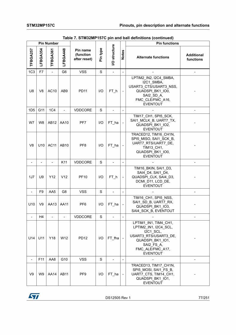
DS12505 Rev 1 77/251
STM32MP157C Pinouts, pin description and alternate functions
123
1C3 F7 - G6 VSS S - - - -
U8 V8 AC10 AB9 PD11 I/O FT_h -
LPTIM2_IN2, I2C4_SMBA, I2C1_SMBA,
USART3_CTS/USART3_NSS, QUADSPI_BK1_IO0,
SAI2_SD_A, FMC_CLE/FMC_A16,
EVENTOUT
-
1D5 G11 1C4 - VDDCORE S - - - -
W7 W8 AB12 AA10 PF7 I/O FT_ha -
TIM17_CH1, SPI5_SCK, SAI1_MCLK_B, UART7_TX,
QUADSPI_BK1_IO2, EVENTOUT
-
V8 U10 AC11 AB10 PF8 I/O FT_ha -
TRACED12, TIM16_CH1N, SPI5_MISO, SAI1_SCK_B, UART7_RTS/UART7_DE,
TIM13_CH1, QUADSPI_BK1_IO0,
EVENTOUT
-
- - - K11 VDDCORE S - - - -
1J7 U9 Y12 V12 PF10 I/O FT_h -
TIM16_BKIN, SAI1_D3, SAI4_D4, SAI1_D4,
QUADSPI_CLK, SAI4_D3, DCMI_D11, LCD_DE,
EVENTOUT
-
- F9 AA5 G8 VSS S - - - -
U10 V9 AA13 AA11 PF6 I/O FT_ha -
TIM16_CH1, SPI5_NSS, SAI1_SD_B, UART7_RX,
QUADSPI_BK1_IO3, SAI4_SCK_B, EVENTOUT
-
- H4 - - VDDCORE S - - - -
U14 U11 Y18 W12 PD12 I/O FT_fha -
LPTIM1_IN1, TIM4_CH1, LPTIM2_IN1, I2C4_SCL,
I2C1_SCL, USART3_RTS/USART3_DE,
QUADSPI_BK1_IO1, SAI2_FS_A,
FMC_ALE/FMC_A17, EVENTOUT
-
- F11 AA8 G10 VSS S - - - -
V9 W9 AA14 AB11 PF9 I/O FT_ha -
TRACED13, TIM17_CH1N, SPI5_MOSI, SAI1_FS_B,
UART7_CTS, TIM14_CH1, QUADSPI_BK1_IO1,
EVENTOUT
-
Table 7. STM32MP157C pin and ball definitions (continued)Pin Number
Pin name (function
after reset) Pin
ty
pe
I/O s
tru
ctu
re
No
tes
Pin functions
TF
BG
A25
7
LF
BG
A35
4
TF
BG
A36
1
LF
BG
A44
8
Alternate functionsAdditional functions

Pinouts, pin description and alternate functions STM32MP157C
78/251 DS12505 Rev 1
- H6 1C6 K13 VDDCORE S - - - -
V11 W10 AC14 Y11 PG7 I/O FT_h -
TRACED5, SAI1_MCLK_A, USART6_CK,
UART8_RTS/UART8_DE, QUADSPI_CLK,
QUADSPI_BK2_IO3, DCMI_D13, LCD_CLK,
EVENTOUT
-
1E3 F15 - G12 VSS S - - - -
1F5 - - - VDDCORE S - - - -
W11 T12 Y14 W13 PB6 I/O FT_fha -
TIM16_CH1N, TIM4_CH1, I2C1_SCL, CEC, I2C4_SCL, USART1_TX, FDCAN2_TX,
QUADSPI_BK1_NCS, DFSDM1_DATIN5, UART5_TX,
DCMI_D5, EVENTOUT
-
U12 T11 AC13 Y12 PE8 I/O FT_h -
TIM1_CH1N, DFSDM1_CKIN2, UART7_TX,
QUADSPI_BK2_IO1, FMC_D5/FMC_DA5,
EVENTOUT
-
V12 V10 Y15 W14 PE10 I/O FT_ha -
TIM1_CH2N, DFSDM1_DATIN4, UART7_CTS,
QUADSPI_BK2_IO3, FMC_D7/FMC_DA7,
EVENTOUT
-
- H8 1D1 K15 VDDCORE S - - - -
V13 T13 Y16 V13 PB2 I/O FT_ha -
TRACED4, RTC_OUT2, SAI1_D1, DFSDM1_CKIN1,
USART1_RX, I2S_CKIN, SAI1_SD_A,
SPI3_MOSI/I2S3_SDO, UART4_RX, QUADSPI_CLK,
EVENTOUT
-
- H10 - - VDDCORE S - - - -
U13 U12 AA19 V14 PD13 I/O FT_fha -
LPTIM1_OUT, TIM4_CH2, I2C4_SDA, I2C1_SDA,
I2S3_MCK, QUADSPI_BK1_IO3,
SAI2_SCK_A, FMC_A18, DSI_TE, EVENTOUT
-
- N7 - - VDD S - - - -
- G2 AA12 G14 VSS S - - - -
1J8 V16 AB18 AA17 USB_RREF A A - - -
Table 7. STM32MP157C pin and ball definitions (continued)Pin Number
Pin name (function
after reset) Pin
ty
pe
I/O s
tru
ctu
re
No
tes
Pin functions
TF
BG
A25
7
LF
BG
A35
4
TF
BG
A36
1
LF
BG
A44
8
Alternate functionsAdditional functions

DS12505 Rev 1 79/251
STM32MP157C Pinouts, pin description and alternate functions
123
- W12 AA15 AB13VDD3V3_USBHS
S - - - -
1H7 - - -VDD3V3_
USBS - - - -
V10 W13 AC16 AB14 USB_DP2 A FT_u - -USBH_HS_DP2,
OTG_HS_DP
W10 V13 AB16 AA14 USB_DM2 A FT_u - -USBH_HS_DM2, OTG_HS_DM
- U13 AA16 Y13 VSS_USBHS S - - - -
- - - Y14 VSS_USBHS S - - - -
U11 T15 AB13 AA12BYPASS_REG1V8
I FT - - -
W8 T14 Y13 W15 PG9 I/O FT_h -
DBTRGO, USART6_RX, SPDIFRX_IN3,
QUADSPI_BK2_IO2, SAI2_FS_B,
FMC_NCE/FMC_NE2, DCMI_VSYNC, LCD_R1,
EVENTOUT
-
1G3 - 1H5 R10 VDD S - - - -
- N9 - - VDD S - - - -
1H5 V11 AB14 AB12VDDA1V8_
REGS - - - -
1H3 - - G17 VSS S - - - -
1J6 W11 AB15 AB17VDDA1V1_
REGS - - - -
- G4 AA21 H7 VSS S - - - -
- - - R12 VDD S - - - -
- P6 - - VDD S - - - -
- U14 - Y15 VSS_USBHS S - - - -
- V12 - AA13 VSS_USBHS S - - - -
1D4 G6 AC1 J9 VSS S - - - -
- V15 - AA16 VSS_USBHS S - - - -
W14 W14 AB17 AB15 USB_DM1 A FT_u - - USBH_HS_DM1
V14 V14 AC17 AA15 USB_DP1 A FT_u - - USBH_HS_DP1
V15 U16 AB19 W16 PA12 I/O FT_uf -
TIM1_ETR, I2C6_SDA, I2C5_SDA, UART4_TX,
USART1_RTS/USART1_DE, SAI2_FS_B, FDCAN1_TX,
LCD_R5, EVENTOUT
OTG_FS_DP
Table 7. STM32MP157C pin and ball definitions (continued)Pin Number
Pin name (function
after reset) Pin
ty
pe
I/O s
tru
ctu
re
No
tes
Pin functions
TF
BG
A25
7
LF
BG
A35
4
TF
BG
A36
1
LF
BG
A44
8
Alternate functionsAdditional functions

Pinouts, pin description and alternate functions STM32MP157C
80/251 DS12505 Rev 1
- G8 - J11 VSS S - - - -
- - - L8 VDDCORE S - - - -
U15 V17 AA18 Y16 PA11 I/O FT_uf -
TIM1_CH4, I2C6_SCL, I2C5_SCL,
SPI2_NSS/I2S2_WS, UART4_RX,
USART1_CTS/USART1_NSS, FDCAN1_RX, LCD_R4,
EVENTOUT
OTG_FS_DM
1C6 H12 1D3 - VDDCORE S - - - -
1F4 G10 AC23 - VSS S - - - -
- W15 AA17 AB16VDD3V3_USBFS
S - - - -
V16 U15 AC19 V15 OTG_VBUS A FT_u - -OTG_FS_VBUS
, OTG_HS_VBUS
U16 T16 Y17 Y17 PA10 I/O FT_u -
TIM1_CH3, SPI3_NSS/I2S3_WS,
USART1_RX, MDIOS_MDIO, SAI4_FS_B, DCMI_D1, LCD_B1, EVENTOUT
OTG_FS_ID, OTG_HS_ID
- - AB20 AB20 DDR_DQ27 I/O DDR - - -
1B9 E15 1A8 E18 VDDQ_DDR S - - - -
- - AB21 AB21 DDR_DQ26 I/O DDR - - -
- G12 - J13 VSS S - - - -
- - AC22 AA21 DDR_DQ28 I/O DDR - - -
1H4 G14 1A3 J17 VSS S - - - -
- - AC21 AA20 DDR_DQ29 I/O DDR - - -
- - Y22 W20 DDR_DQ25 I/O DDR - - -
- - AB22 Y21 DDR_DQS3P I/O DDR - - -
- H5 - J20 VSS S - - - -
- - AB23 Y22 DDR_DQS3N I/O DDR - - -
- - - F17 VDDQ_DDR S - - - -
- - AA20 AA22 DDR_DQM3 O DDR - - -
- F14 1B7 - VDDQ_DDR S - - - -
- - AA22 W21 DDR_DQ31 I/O DDR - - -
- H7 1A5 K3 VSS S - - - -
Table 7. STM32MP157C pin and ball definitions (continued)Pin Number
Pin name (function
after reset) Pin
ty
pe
I/O s
tru
ctu
re
No
tes
Pin functions
TF
BG
A25
7
LF
BG
A35
4
TF
BG
A36
1
LF
BG
A44
8
Alternate functionsAdditional functions
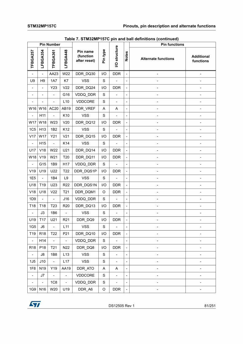
DS12505 Rev 1 81/251
STM32MP157C Pinouts, pin description and alternate functions
123
- - AA23 W22 DDR_DQ30 I/O DDR - - -
U9 H9 1A7 K7 VSS S - - - -
- - Y23 V22 DDR_DQ24 I/O DDR - - -
- - - G16 VDDQ_DDR S - - - -
- - - L10 VDDCORE S - - - -
W16 W16 AC20 AB19 DDR_VREF A A - - -
- H11 - K10 VSS S - - - -
W17 W18 W23 V20 DDR_DQ12 I/O DDR - - -
1C5 H13 1B2 K12 VSS S - - - -
V17 W17 Y21 V21 DDR_DQ15 I/O DDR - - -
- H15 - K14 VSS S - - - -
U17 V18 W22 U21 DDR_DQ14 I/O DDR - - -
W18 V19 W21 T20 DDR_DQ11 I/O DDR - - -
- G15 1B9 H17 VDDQ_DDR S - - - -
V19 U19 U22 T22 DDR_DQS1P I/O DDR - - -
1E5 - 1B4 L9 VSS S - - - -
U18 T19 U23 R22 DDR_DQS1N I/O DDR - - -
V18 U18 V22 T21 DDR_DQM1 O DDR - - -
1D9 - - J16 VDDQ_DDR S - - - -
T18 T18 T23 R20 DDR_DQ13 I/O DDR - - -
- J3 1B6 - VSS S - - - -
U19 T17 U21 R21 DDR_DQ9 I/O DDR - - -
1G5 J6 - L11 VSS S - - - -
T19 R18 T22 P21 DDR_DQ10 I/O DDR - - -
- H14 - - VDDQ_DDR S - - - -
R18 P18 T21 N22 DDR_DQ8 I/O DDR - - -
- J8 1B8 L13 VSS S - - - -
1J5 J10 - L17 VSS S - - - -
1F8 N19 Y19 AA19 DDR_ATO A A - - -
- J7 - - VDDCORE S - - - -
- - 1C8 - VDDQ_DDR S - - - -
1G9 N16 W20 U19 DDR_A6 O DDR - - -
Table 7. STM32MP157C pin and ball definitions (continued)Pin Number
Pin name (function
after reset) Pin
ty
pe
I/O s
tru
ctu
re
No
tes
Pin functions
TF
BG
A25
7
LF
BG
A35
4
TF
BG
A36
1
LF
BG
A44
8
Alternate functionsAdditional functions

Pinouts, pin description and alternate functions STM32MP157C
82/251 DS12505 Rev 1
- - - K17 VDDQ_DDR S - - - -
T17 R17 Y20 U18 DDR_A8 O DDR - - -
- J12 1C1 L19 VSS S - - - -
R17 P17 V20 T18 DDR_A4 O DDR - - -
1A6 J14 1C3 L20 VSS S - - - -
P17 P19 T20 R19 DDR_CKE O DDR - - -
P18 N17 U20 R18 DDR_BA1 O DDR - - -
- J15 - L16 VDDQ_DDR S - - - -
N18 N18 R21 P18 DDR_A14 O DDR - - -
- K2 - M7 VSS S - - - -
N19 M18 R20 P19 DDR_A11 O DDR - - -
- K5 1C5 M10 VSS S - - - -
1D6 K7 - M12 VSS S - - - -
M17 M19 R22 N18 DDR_A10 O DDR - - -
- J9 1D5 L12 VDDCORE S - - - -
- - 1D9 - VDDQ_DDR S - - - -
M18 L17 P23 N19 DDR_A12 O DDR - - -
M19 M17 P22 M18 DDR_A1 O DDR - - -
- K9 1C7 M14 VSS S - - - -
J19 K17 N20 M22 DDR_CASN O DDR - - -
1F6 K11 - N9 VSS S - - - -
J18 J17 M20 M21 DDR_WEN O DDR - - -
- K14 - M17 VDDQ_DDR S - - - -
1E9 L18 N21 M20 DDR_RASN O DDR - - -
L17 L19 N22 N20 DDR_CLKP O DDR - - -
- K13 1C9 - VSS S - - - -
K18 K19 N23 N21 DDR_CLKN O DDR - - -
1F9 - 1E8 N16 VDDQ_DDR S - - - -
1D8 K18 K20 L22 DDR_DTO0 O DDR - - -
1C8 J19 L21 K21 DDR_DTO1 O DDR - - -
L18 L16 P20 M19 DDR_A15 O DDR - - -
1H6 - 1D2 N11 VSS S - - - -
Table 7. STM32MP157C pin and ball definitions (continued)Pin Number
Pin name (function
after reset) Pin
ty
pe
I/O s
tru
ctu
re
No
tes
Pin functions
TF
BG
A25
7
LF
BG
A35
4
TF
BG
A36
1
LF
BG
A44
8
Alternate functionsAdditional functions

DS12505 Rev 1 83/251
STM32MP157C Pinouts, pin description and alternate functions
123
1E6 - - - VDDCORE S - - - -
- K15 - N13 VSS S - - - -
J17 J18 M22 L18 DDR_CSN O DDR - - -
H18 H19 L22 L21 DDR_ODT O DDR - - -
H17 J16 M21 K18 DDR_BA2 O DDR - - -
1C7 L6 1D4 N17 VSS S - - - -
G18 H18 L20 K19 DDR_A0 O DDR - - -
- L15 - P17 VDDQ_DDR S - - - -
G19 G19 L23 K20 DDR_BA0 O DDR - - -
E17 F17 F20 G18 DDR_A13 O DDR - - -
- L8 - P3 VSS S - - - -
F17 G18 J20 J18 DDR_A2 O DDR - - -
1E7 L10 1D6 P7 VSS S - - - -
F19 F19 K22 J19 DDR_A3 O DDR - - -
- - 1F9 - VDDQ_DDR S - - - -
C16 G16 D20 F19DDR_
RESETNO DDR - - -
- M14 - R16 VDDQ_DDR S - - - -
1C9 H17 H20 H19 DDR_A5 O DDR - - -
- L12 1D8 P10 VSS S - - - -
1A9 E17 E20 F18 DDR_A7 O DDR - - -
- L14 - P12 VSS S - - - -
1A8 F18 K23 K22 DDR_ZQ A A - - -
E18 G17 G20 H18 DDR_A9 O DDR - - -
1G7 M5 1E1 P14 VSS S - - - -
- J11 1D7 L14 VDDCORE S - - - -
D18 E18 J21 J21 DDR_DQ4 I/O DDR - - -
- M7 - P20 VSS S - - - -
D19 D17 J22 H20 DDR_DQ5 I/O DDR - - -
W13 M9 1E3 - VSS S - - - -
C18 D18 H21 H21 DDR_DQ2 I/O DDR - - -
- - - T17 VDDQ_DDR S - - - -
Table 7. STM32MP157C pin and ball definitions (continued)Pin Number
Pin name (function
after reset) Pin
ty
pe
I/O s
tru
ctu
re
No
tes
Pin functions
TF
BG
A25
7
LF
BG
A35
4
TF
BG
A36
1
LF
BG
A44
8
Alternate functionsAdditional functions

Pinouts, pin description and alternate functions STM32MP157C
84/251 DS12505 Rev 1
C19 D19 H22 H22 DDR_DQ6 I/O DDR - - -
- - 1G8 - VDDQ_DDR S - - - -
B19 C19 G22 G22 DDR_DQS0P I/O DDR - - -
- M11 - R8 VSS S - - - -
B18 B19 G23 G21 DDR_DQS0N I/O DDR - - -
- N15 - - VDDQ_DDR S - - - -
C17 C18 H23 G20 DDR_DQM0 O DDR - - -
1H9 - - U16 VDDQ_DDR S - - - -
B17 B18 G21 G19 DDR_DQ7 I/O DDR - - -
1B8 M13 1E5 R17 VSS S - - - -
A18 A18 F22 F21 DDR_DQ1 I/O DDR - - -
- M15 1E7 T7 VSS S - - - -
A17 A17 E22 E21 DDR_DQ0 I/O DDR - - -
B16 B17 E21 E20 DDR_DQ3 I/O DDR - - -
- P14 1H9 V17 VDDQ_DDR S - - - -
1H8 - - T9 VSS S - - - -
- J13 - - VDDCORE S - - - -
- - E23 E22 DDR_DQ21 I/O DDR - - -
- N6 1E9 T11 VSS S - - - -
- - D21 D20 DDR_DQ22 I/O DDR - - -
C14 N8 - T19 VSS S - - - -
- - D22 D21 DDR_DQ17 I/O DDR - - -
- - D23 D22 DDR_DQ18 I/O DDR - - -
- - - W18 VDDQ_DDR S - - - -
- - C22 C21 DDR_DQS2P I/O DDR - - -
- N10 1F2 U7 VSS S - - - -
- - B23 B22 DDR_DQS2N I/O DDR - - -
- R15 1J8 - VDDQ_DDR S - - - -
- - C23 C22 DDR_DQM2 O DDR - - -
- - - Y19 VDDQ_DDR S - - - -
- - B22 B21 DDR_DQ16 I/O DDR - - -
- N12 1F4 U13 VSS S - - - -
Table 7. STM32MP157C pin and ball definitions (continued)Pin Number
Pin name (function
after reset) Pin
ty
pe
I/O s
tru
ctu
re
No
tes
Pin functions
TF
BG
A25
7
LF
BG
A35
4
TF
BG
A36
1
LF
BG
A44
8
Alternate functionsAdditional functions
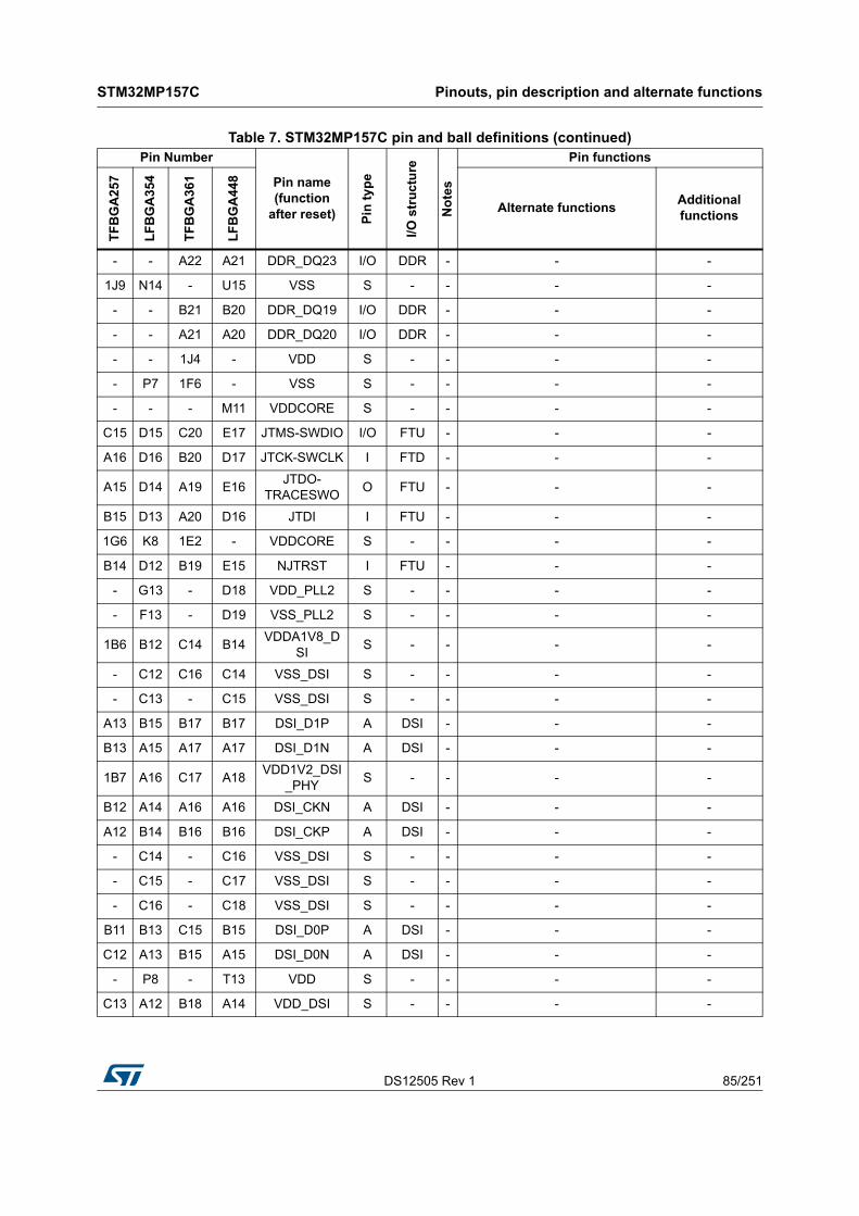
DS12505 Rev 1 85/251
STM32MP157C Pinouts, pin description and alternate functions
123
- - A22 A21 DDR_DQ23 I/O DDR - - -
1J9 N14 - U15 VSS S - - - -
- - B21 B20 DDR_DQ19 I/O DDR - - -
- - A21 A20 DDR_DQ20 I/O DDR - - -
- - 1J4 - VDD S - - - -
- P7 1F6 - VSS S - - - -
- - - M11 VDDCORE S - - - -
C15 D15 C20 E17 JTMS-SWDIO I/O FTU - - -
A16 D16 B20 D17 JTCK-SWCLK I FTD - - -
A15 D14 A19 E16JTDO-
TRACESWOO FTU - - -
B15 D13 A20 D16 JTDI I FTU - - -
1G6 K8 1E2 - VDDCORE S - - - -
B14 D12 B19 E15 NJTRST I FTU - - -
- G13 - D18 VDD_PLL2 S - - - -
- F13 - D19 VSS_PLL2 S - - - -
1B6 B12 C14 B14VDDA1V8_D
SIS - - - -
- C12 C16 C14 VSS_DSI S - - - -
- C13 - C15 VSS_DSI S - - - -
A13 B15 B17 B17 DSI_D1P A DSI - - -
B13 A15 A17 A17 DSI_D1N A DSI - - -
1B7 A16 C17 A18VDD1V2_DSI
_PHYS - - - -
B12 A14 A16 A16 DSI_CKN A DSI - - -
A12 B14 B16 B16 DSI_CKP A DSI - - -
- C14 - C16 VSS_DSI S - - - -
- C15 - C17 VSS_DSI S - - - -
- C16 - C18 VSS_DSI S - - - -
B11 B13 C15 B15 DSI_D0P A DSI - - -
C12 A13 B15 A15 DSI_D0N A DSI - - -
- P8 - T13 VDD S - - - -
C13 A12 B18 A14 VDD_DSI S - - - -
Table 7. STM32MP157C pin and ball definitions (continued)Pin Number
Pin name (function
after reset) Pin
ty
pe
I/O s
tru
ctu
re
No
tes
Pin functions
TF
BG
A25
7
LF
BG
A35
4
TF
BG
A36
1
LF
BG
A44
8
Alternate functionsAdditional functions
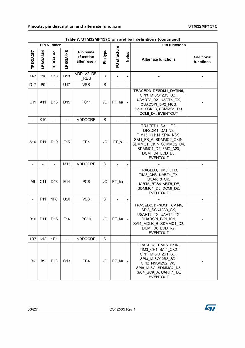
Pinouts, pin description and alternate functions STM32MP157C
86/251 DS12505 Rev 1
1A7 B16 C18 B18VDD1V2_DSI
_REGS - - - -
D17 P9 - U17 VSS S - - - -
C11 A11 D16 D15 PC11 I/O FT_ha -
TRACED3, DFSDM1_DATIN5, SPI3_MISO/I2S3_SDI,
USART3_RX, UART4_RX, QUADSPI_BK2_NCS,
SAI4_SCK_B, SDMMC1_D3, DCMI_D4, EVENTOUT
-
- K10 - - VDDCORE S - - - -
A10 B11 D19 F15 PE4 I/O FT_h -
TRACED1, SAI1_D2, DFSDM1_DATIN3,
TIM15_CH1N, SPI4_NSS, SAI1_FS_A, SDMMC2_CKIN,
SDMMC1_CKIN, SDMMC2_D4, SDMMC1_D4, FMC_A20,
DCMI_D4, LCD_B0, EVENTOUT
-
- - - M13 VDDCORE S - - - -
A9 C11 D18 E14 PC8 I/O FT_ha -
TRACED0, TIM3_CH3, TIM8_CH3, UART4_TX,
USART6_CK, UART5_RTS/UART5_DE, SDMMC1_D0, DCMI_D2,
EVENTOUT
-
- P11 1F8 U20 VSS S - - - -
B10 D11 D15 F14 PC10 I/O FT_ha -
TRACED2, DFSDM1_CKIN5, SPI3_SCK/I2S3_CK,
USART3_TX, UART4_TX, QUADSPI_BK1_IO1,
SAI4_MCLK_B, SDMMC1_D2, DCMI_D8, LCD_R2,
EVENTOUT
-
1D7 K12 1E4 - VDDCORE S - - - -
B6 B9 B13 C13 PB4 I/O FT_ha -
TRACED8, TIM16_BKIN, TIM3_CH1, SAI4_CK2, SPI1_MISO/I2S1_SDI, SPI3_MISO/I2S3_SDI, SPI2_NSS/I2S2_WS,
SPI6_MISO, SDMMC2_D3, SAI4_SCK_A, UART7_TX,
EVENTOUT
-
Table 7. STM32MP157C pin and ball definitions (continued)Pin Number
Pin name (function
after reset) Pin
ty
pe
I/O s
tru
ctu
re
No
tes
Pin functions
TF
BG
A25
7
LF
BG
A35
4
TF
BG
A36
1
LF
BG
A44
8
Alternate functionsAdditional functions
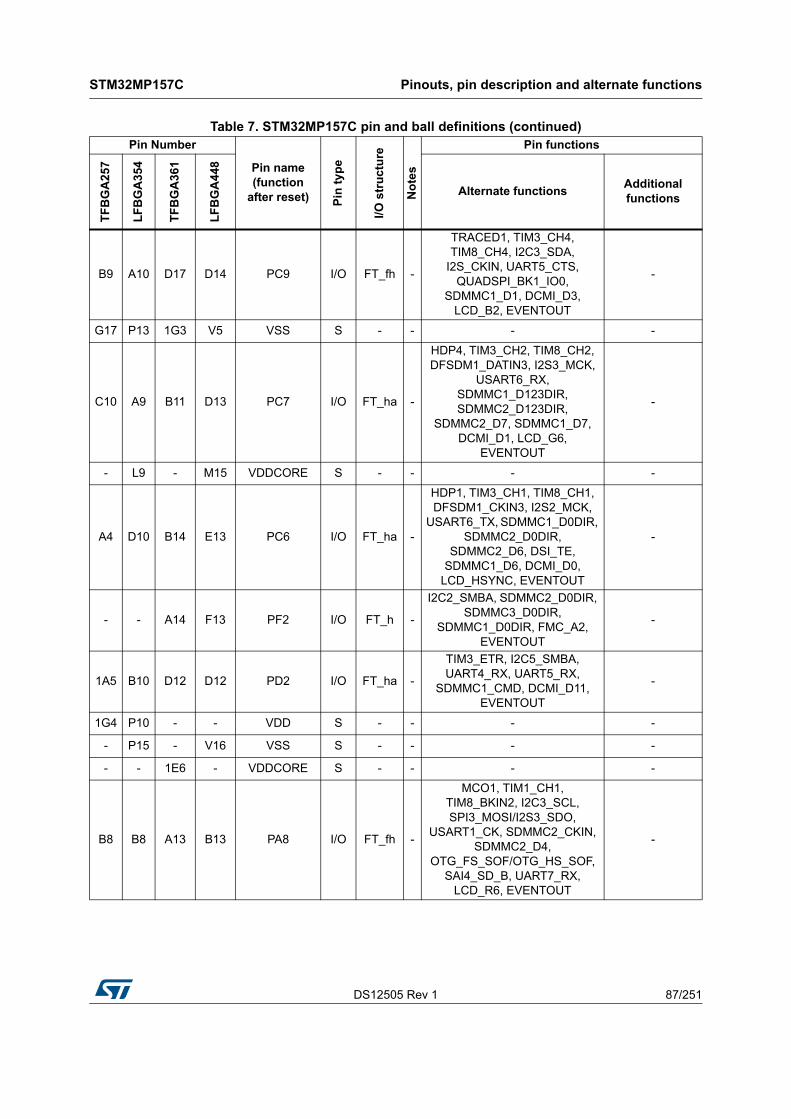
DS12505 Rev 1 87/251
STM32MP157C Pinouts, pin description and alternate functions
123
B9 A10 D17 D14 PC9 I/O FT_fh -
TRACED1, TIM3_CH4, TIM8_CH4, I2C3_SDA,
I2S_CKIN, UART5_CTS, QUADSPI_BK1_IO0,
SDMMC1_D1, DCMI_D3, LCD_B2, EVENTOUT
-
G17 P13 1G3 V5 VSS S - - - -
C10 A9 B11 D13 PC7 I/O FT_ha -
HDP4, TIM3_CH2, TIM8_CH2, DFSDM1_DATIN3, I2S3_MCK,
USART6_RX, SDMMC1_D123DIR, SDMMC2_D123DIR,
SDMMC2_D7, SDMMC1_D7, DCMI_D1, LCD_G6,
EVENTOUT
-
- L9 - M15 VDDCORE S - - - -
A4 D10 B14 E13 PC6 I/O FT_ha -
HDP1, TIM3_CH1, TIM8_CH1, DFSDM1_CKIN3, I2S2_MCK,
USART6_TX, SDMMC1_D0DIR, SDMMC2_D0DIR,
SDMMC2_D6, DSI_TE, SDMMC1_D6, DCMI_D0,
LCD_HSYNC, EVENTOUT
-
- - A14 F13 PF2 I/O FT_h -
I2C2_SMBA, SDMMC2_D0DIR, SDMMC3_D0DIR,
SDMMC1_D0DIR, FMC_A2, EVENTOUT
-
1A5 B10 D12 D12 PD2 I/O FT_ha -
TIM3_ETR, I2C5_SMBA, UART4_RX, UART5_RX,
SDMMC1_CMD, DCMI_D11, EVENTOUT
-
1G4 P10 - - VDD S - - - -
- P15 - V16 VSS S - - - -
- - 1E6 - VDDCORE S - - - -
B8 B8 A13 B13 PA8 I/O FT_fh -
MCO1, TIM1_CH1, TIM8_BKIN2, I2C3_SCL, SPI3_MOSI/I2S3_SDO,
USART1_CK, SDMMC2_CKIN, SDMMC2_D4,
OTG_FS_SOF/OTG_HS_SOF, SAI4_SD_B, UART7_RX,
LCD_R6, EVENTOUT
-
Table 7. STM32MP157C pin and ball definitions (continued)Pin Number
Pin name (function
after reset) Pin
ty
pe
I/O s
tru
ctu
re
No
tes
Pin functions
TF
BG
A25
7
LF
BG
A35
4
TF
BG
A36
1
LF
BG
A44
8
Alternate functionsAdditional functions
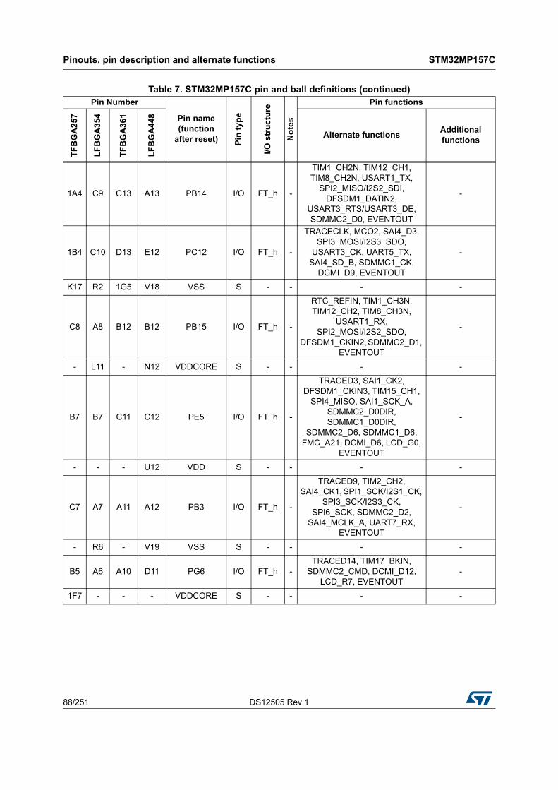
Pinouts, pin description and alternate functions STM32MP157C
88/251 DS12505 Rev 1
1A4 C9 C13 A13 PB14 I/O FT_h -
TIM1_CH2N, TIM12_CH1, TIM8_CH2N, USART1_TX,
SPI2_MISO/I2S2_SDI, DFSDM1_DATIN2,
USART3_RTS/USART3_DE, SDMMC2_D0, EVENTOUT
-
1B4 C10 D13 E12 PC12 I/O FT_h -
TRACECLK, MCO2, SAI4_D3, SPI3_MOSI/I2S3_SDO,
USART3_CK, UART5_TX, SAI4_SD_B, SDMMC1_CK,
DCMI_D9, EVENTOUT
-
K17 R2 1G5 V18 VSS S - - - -
C8 A8 B12 B12 PB15 I/O FT_h -
RTC_REFIN, TIM1_CH3N, TIM12_CH2, TIM8_CH3N,
USART1_RX, SPI2_MOSI/I2S2_SDO,
DFSDM1_CKIN2, SDMMC2_D1, EVENTOUT
-
- L11 - N12 VDDCORE S - - - -
B7 B7 C11 C12 PE5 I/O FT_h -
TRACED3, SAI1_CK2, DFSDM1_CKIN3, TIM15_CH1,
SPI4_MISO, SAI1_SCK_A, SDMMC2_D0DIR, SDMMC1_D0DIR,
SDMMC2_D6, SDMMC1_D6, FMC_A21, DCMI_D6, LCD_G0,
EVENTOUT
-
- - - U12 VDD S - - - -
C7 A7 A11 A12 PB3 I/O FT_h -
TRACED9, TIM2_CH2, SAI4_CK1, SPI1_SCK/I2S1_CK,
SPI3_SCK/I2S3_CK, SPI6_SCK, SDMMC2_D2,
SAI4_MCLK_A, UART7_RX, EVENTOUT
-
- R6 - V19 VSS S - - - -
B5 A6 A10 D11 PG6 I/O FT_h -TRACED14, TIM17_BKIN,
SDMMC2_CMD, DCMI_D12, LCD_R7, EVENTOUT
-
1F7 - - - VDDCORE S - - - -
Table 7. STM32MP157C pin and ball definitions (continued)Pin Number
Pin name (function
after reset) Pin
ty
pe
I/O s
tru
ctu
re
No
tes
Pin functions
TF
BG
A25
7
LF
BG
A35
4
TF
BG
A36
1
LF
BG
A44
8
Alternate functionsAdditional functions

DS12505 Rev 1 89/251
STM32MP157C Pinouts, pin description and alternate functions
123
A7 C6 D14 B11 PD3 I/O FT_h -
HDP5, DFSDM1_CKOUT, SPI2_SCK/I2S2_CK, DFSDM1_DATIN0,
USART2_CTS/USART2_NSS, SDMMC1_D123DIR,
SDMMC2_D7, SDMMC2_D123DIR,
SDMMC1_D7, FMC_CLK, DCMI_D5, LCD_G7,
EVENTOUT
-
C9 D9 B10 F12 PB9 I/O FT_fh -
HDP7, TIM17_CH1, TIM4_CH4, DFSDM1_DATIN7, I2C1_SDA,
SPI2_NSS/I2S2_WS, I2C4_SDA, SDMMC2_CDIR,
UART4_TX, FDCAN1_TX, SDMMC2_D5, SDMMC1_CDIR,
SDMMC1_D5, DCMI_D7, LCD_B7, EVENTOUT
-
B4 C7 C19 E11 PA15 I/O FT_h -
DBTRGI, TIM2_CH1/TIM2_ETR, SAI4_D2, SDMMC1_CDIR, CEC, SPI1_NSS/I2S1_WS,
SPI3_NSS/I2S3_WS, SPI6_NSS,
UART4_RTS/UART4_DE, SDMMC2_D5, SDMMC2_CDIR,
SDMMC1_D5, SAI4_FS_A, UART7_TX, LCD_R1,
EVENTOUT
-
N17 - 1G7 W17 VSS S - - - -
C6 C8 A8 A11 PA9 I/O FT_h -
TIM1_CH2, I2C3_SMBA, SPI2_SCK/I2S2_CK,
USART1_TX, SDMMC2_CDIR, SDMMC2_D5, DCMI_D0,
LCD_R5, EVENTOUT
-
A3 B5 D11 F11 PB7 I/O FT_fh -
TIM17_CH1N, TIM4_CH2, I2C1_SDA, I2C4_SDA,
USART1_RX, SDMMC2_D1, DFSDM1_CKIN5, FMC_NL, DCMI_VSYNC, EVENTOUT
-
- L13 1F5 N14 VDDCORE S - - - -
A2 A4 B9 B10 PD1 I/O FT_fh -
I2C6_SCL, DFSDM1_DATIN6, I2C5_SCL, SAI3_SD_A,
UART4_TX, FDCAN1_TX, SDMMC3_D0, DFSDM1_CKIN7,
FMC_D3/FMC_DA3, EVENTOUT
-
- R9 1J6 - VDD S - - - -
Table 7. STM32MP157C pin and ball definitions (continued)Pin Number
Pin name (function
after reset) Pin
ty
pe
I/O s
tru
ctu
re
No
tes
Pin functions
TF
BG
A25
7
LF
BG
A35
4
TF
BG
A36
1
LF
BG
A44
8
Alternate functionsAdditional functions
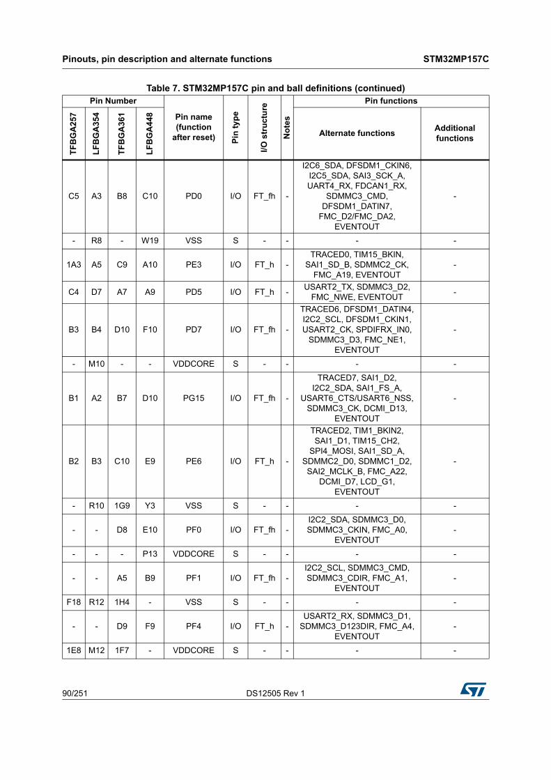
Pinouts, pin description and alternate functions STM32MP157C
90/251 DS12505 Rev 1
C5 A3 B8 C10 PD0 I/O FT_fh -
I2C6_SDA, DFSDM1_CKIN6, I2C5_SDA, SAI3_SCK_A, UART4_RX, FDCAN1_RX,
SDMMC3_CMD, DFSDM1_DATIN7,
FMC_D2/FMC_DA2, EVENTOUT
-
- R8 - W19 VSS S - - - -
1A3 A5 C9 A10 PE3 I/O FT_h -TRACED0, TIM15_BKIN,
SAI1_SD_B, SDMMC2_CK, FMC_A19, EVENTOUT
-
C4 D7 A7 A9 PD5 I/O FT_h -USART2_TX, SDMMC3_D2,
FMC_NWE, EVENTOUT-
B3 B4 D10 F10 PD7 I/O FT_fh -
TRACED6, DFSDM1_DATIN4, I2C2_SCL, DFSDM1_CKIN1, USART2_CK, SPDIFRX_IN0,
SDMMC3_D3, FMC_NE1, EVENTOUT
-
- M10 - - VDDCORE S - - - -
B1 A2 B7 D10 PG15 I/O FT_fh -
TRACED7, SAI1_D2, I2C2_SDA, SAI1_FS_A,
USART6_CTS/USART6_NSS, SDMMC3_CK, DCMI_D13,
EVENTOUT
-
B2 B3 C10 E9 PE6 I/O FT_h -
TRACED2, TIM1_BKIN2, SAI1_D1, TIM15_CH2,
SPI4_MOSI, SAI1_SD_A, SDMMC2_D0, SDMMC1_D2, SAI2_MCLK_B, FMC_A22,
DCMI_D7, LCD_G1, EVENTOUT
-
- R10 1G9 Y3 VSS S - - - -
- - D8 E10 PF0 I/O FT_fh -I2C2_SDA, SDMMC3_D0, SDMMC3_CKIN, FMC_A0,
EVENTOUT-
- - - P13 VDDCORE S - - - -
- - A5 B9 PF1 I/O FT_fh -I2C2_SCL, SDMMC3_CMD, SDMMC3_CDIR, FMC_A1,
EVENTOUT-
F18 R12 1H4 - VSS S - - - -
- - D9 F9 PF4 I/O FT_h -USART2_RX, SDMMC3_D1,
SDMMC3_D123DIR, FMC_A4, EVENTOUT
-
1E8 M12 1F7 - VDDCORE S - - - -
Table 7. STM32MP157C pin and ball definitions (continued)Pin Number
Pin name (function
after reset) Pin
ty
pe
I/O s
tru
ctu
re
No
tes
Pin functions
TF
BG
A25
7
LF
BG
A35
4
TF
BG
A36
1
LF
BG
A44
8
Alternate functionsAdditional functions
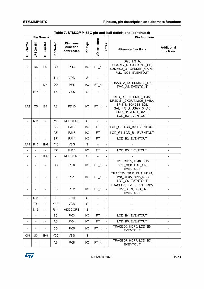
DS12505 Rev 1 91/251
STM32MP157C Pinouts, pin description and alternate functions
123
C3 D6 B6 C9 PD4 I/O FT_h -
SAI3_FS_A, USART2_RTS/USART2_DE,
SDMMC3_D1, DFSDM1_CKIN0, FMC_NOE, EVENTOUT
-
- - - U14 VDD S - - - -
- - D7 D9 PF5 I/O FT_h -USART2_TX, SDMMC3_D2,
FMC_A5, EVENTOUT-
- R14 - Y7 VSS S - - - -
1A2 C5 B5 A8 PD10 I/O FT_h -
RTC_REFIN, TIM16_BKIN, DFSDM1_CKOUT, I2C5_SMBA,
SPI3_MISO/I2S3_SDI, SAI3_FS_B, USART3_CK,
FMC_D15/FMC_DA15, LCD_B3, EVENTOUT
-
- N11 - P15 VDDCORE S - - - -
- - - B8 PJ12 I/O FT - LCD_G3, LCD_B0, EVENTOUT -
- - - A7 PJ13 I/O FT - LCD_G4, LCD_B1, EVENTOUT -
- - - B7 PJ14 I/O FT - LCD_B2, EVENTOUT -
A19 R16 1H6 Y10 VSS S - - - -
- - - C7 PJ15 I/O FT - LCD_B3, EVENTOUT -
- - 1G6 - VDDCORE S - - - -
- - - D8 PK0 I/O FT_h -TIM1_CH1N, TIM8_CH3,
SPI5_SCK, LCD_G5, EVENTOUT
-
- - - E7 PK1 I/O FT_h -TRACED4, TIM1_CH1, HDP4,
TIM8_CH3N, SPI5_NSS, LCD_G6, EVENTOUT
-
- - - E8 PK2 I/O FT_h -TRACED5, TIM1_BKIN, HDP5,
TIM8_BKIN, LCD_G7, EVENTOUT
-
- R11 - - VDD S - - - -
- T4 - Y18 VSS S - - - -
- N13 - R14 VDDCORE S - - - -
- - - B6 PK3 I/O FT - LCD_B4, EVENTOUT -
- - - A6 PK4 I/O FT - LCD_B5, EVENTOUT -
- - - C6 PK5 I/O FT_h -TRACED6, HDP6, LCD_B6,
EVENTOUT-
K19 U3 1H8 Y20 VSS S - - - -
- - - A5 PK6 I/O FT_h -TRACED7, HDP7, LCD_B7,
EVENTOUT-
Table 7. STM32MP157C pin and ball definitions (continued)Pin Number
Pin name (function
after reset) Pin
ty
pe
I/O s
tru
ctu
re
No
tes
Pin functions
TF
BG
A25
7
LF
BG
A35
4
TF
BG
A36
1
LF
BG
A44
8
Alternate functionsAdditional functions

Pinouts, pin description and alternate functions STM32MP157C
92/251 DS12505 Rev 1
1G8 P12 - - VDDCORE S - - - -
- - - B5 PK7 I/O FT - LCD_DE, EVENTOUT -
C2 C4 D6 C5 PE0 I/O FT_h -
LPTIM1_ETR, TIM4_ETR, LPTIM2_ETR,
SPI3_SCK/I2S3_CK, SAI4_MCLK_B, UART8_RX, SAI2_MCLK_A, FMC_NBL0,
DCMI_D2, EVENTOUT
-
1A1 B1 C8 D7 PE1 I/O FT -
LPTIM1_IN2, I2S2_MCK, SAI3_SD_B, UART8_TX, FMC_NBL1, DCMI_D3,
EVENTOUT
-
- U6 1J3 AA4 VSS S - - - -
- - D5 D6 PH8 I/O FT_f -TIM5_ETR, I2C3_SDA,
DCMI_HSYNC, LCD_R2, EVENTOUT
-
- - 1H7 T15 VDDCORE S - - - -
- - C5 E6 PH9 I/O FT -TIM12_CH2, I2C3_SMBA,
DCMI_D0, LCD_R3, EVENTOUT
-
D2 C1 A4 D5 PE11 I/O FT -
TIM1_CH2, DFSDM1_CKIN4, SPI4_NSS, USART6_CK,
SAI2_SD_B, FMC_D8/FMC_DA8, DCMI_D4,
LCD_G3, EVENTOUT
-
C1 D2 B4 E4 PE12 I/O FT_h -
TIM1_CH3N, DFSDM1_DATIN5, SPI4_SCK, SDMMC1_D0DIR,
SAI2_SCK_B, FMC_D9/FMC_DA9, LCD_B4,
EVENTOUT
-
E3 C2 A3 A4 PE13 I/O FT_h -
HDP2, TIM1_CH3, DFSDM1_CKIN5, SPI4_MISO,
SAI2_FS_B, FMC_D10/FMC_DA10,
DCMI_D6, LCD_DE, EVENTOUT
-
- R13 - - VDDCORE S - - - -
- - C4 B3 PH11 I/O FT_f -TIM5_CH2, I2C4_SCL,
I2C1_SCL, DCMI_D2, LCD_R5, EVENTOUT
-
R19 U8 - AA18 VSS S - - - -
- U17 1J5 AB1 VSS S - - - -
W19 W1 - AB18 VSS S - - - -
Table 7. STM32MP157C pin and ball definitions (continued)Pin Number
Pin name (function
after reset) Pin
ty
pe
I/O s
tru
ctu
re
No
tes
Pin functions
TF
BG
A25
7
LF
BG
A35
4
TF
BG
A36
1
LF
BG
A44
8
Alternate functionsAdditional functions

DS12505 Rev 1 93/251
STM32MP157C Pinouts, pin description and alternate functions
123
- W19 1J7 AB22 VSS S - - - -
1B2 D3 C6 B4 PE14 I/O FT_h -
TIM1_CH4, SPI4_MOSI, UART8_RTS/UART8_DE,
SAI2_MCLK_B, SDMMC1_D123DIR,
FMC_D11/FMC_DA11, LCD_G0, LCD_CLK, EVENTOUT
-
D3 E1 D3 C4 PE15 I/O FT -
HDP3, TIM1_BKIN, TIM15_BKIN,
USART2_CTS/USART2_NSS, UART8_CTS, FMC_NCE2,
FMC_D12/FMC_DA12, LCD_R7, EVENTOUT
-
- - B3 A3 PH4 I/O FT_f -I2C2_SCL, LCD_G5, LCD_G4,
EVENTOUT-
Table 7. STM32MP157C pin and ball definitions (continued)Pin Number
Pin name (function
after reset) Pin
ty
pe
I/O s
tru
ctu
re
No
tes
Pin functions
TF
BG
A25
7
LF
BG
A35
4
TF
BG
A36
1
LF
BG
A44
8
Alternate functionsAdditional functions

Pin
ou
ts, p
in d
esc
riptio
n a
nd
altern
ate
fun
ctio
ns
ST
M3
2M
P15
7C
94/2
51D
S1
2505 R
ev 1
Table 8. Alternate function AF0 to AF7(1)
Port
AF0 AF1 AF2 AF3 AF4 AF5 AF6 AF7
HDP/SYS/RTCTIM1/2/16/17/LPTIM1/SYS/
RTC
SAI1/4/I2C6/TIM3/4/5/12/
HDP/SYS
SAI4/I2C2/TIM8/
LPTIM2/3/4/5/DFSDM1/SDMMC1
SAI4/I2C1/2/3/4/5/
USART1/TIM15/LPTIM2/DFSDM1/CEC
SPI1/I2S1/SPI2/I2S2/SPI3/I2S3/
SPI4/5/6/I2C1/SDMMC1/3/
CEC
SPI3/I2S3/SAI1/3/4/
I2C4/UART4/DFSDM1
SPI2/I2S2/SPI3/I2S3/
SPI6/USART1/2/3/6/
UART7/SDMMC2
Port A
PA0 -TIM2_CH1/TIM2_ETR
TIM5_CH1 TIM8_ETR TIM15_BKIN - -USART2_CTS/USART2_NSS
PA1 ETH_CLK TIM2_CH2 TIM5_CH2 LPTIM3_OUT TIM15_CH1N - -USART2_RTS/USART2_DE
PA2 - TIM2_CH3 TIM5_CH3 LPTIM4_OUT TIM15_CH1 - - USART2_TX
PA3 - TIM2_CH4 TIM5_CH4 LPTIM5_OUT TIM15_CH2 - - USART2_RX
PA4 HDP0 - TIM5_ETR - SAI4_D2SPI1_NSS/I2S1_WS
SPI3_NSS/I2S3_WS
USART2_CK
PA5 -TIM2_CH1/TIM2_ETR
- TIM8_CH1N SAI4_CK1SPI1_SCK/I2S1
_CK- -
PA6 - TIM1_BKIN TIM3_CH1 TIM8_BKIN SAI4_CK2SPI1_MISO/
I2S1_SDI- -
PA7 - TIM1_CH1N TIM3_CH2 TIM8_CH1N SAI4_D1SPI1_MOSI/I2S1_SDO
- -
PA8 MCO1 TIM1_CH1 - TIM8_BKIN2 I2C3_SCLSPI3_MOSI/I2S3_SDO
- USART1_CK
PA9 - TIM1_CH2 - - I2C3_SMBASPI2_SCK/I2S2_CK
- USART1_TX
PA10 - TIM1_CH3 - - -SPI3_NSS/I2S3_WS
- USART1_RX
PA11 - TIM1_CH4 I2C6_SCL - I2C5_SCLSPI2_NSS/I2S2_WS
UART4_RXUSART1_CTS/USART1_NSS
PA12 - TIM1_ETR I2C6_SDA - I2C5_SDA - UART4_TXUSART1_RTS/USART1_DE

ST
M3
2MP
157
CP
ino
uts
, pin
des
criptio
n a
nd
alte
rna
te fu
nc
tion
s
DS
1250
5 Rev 1
95/251
Port A
PA13 DBTRGO DBTRGI MCO1 - - - - -
PA14 DBTRGO DBTRGI MCO2 - - - - -
PA15 DBTRGITIM2_CH1/TIM2_ETR
SAI4_D2SDMMC1_
CDIRCEC
SPI1_NSS/I2S1_WS
SPI3_NSS/I2S3_WS
SPI6_NSS
Port B
PB0 - TIM1_CH2N TIM3_CH3 TIM8_CH2N - -DFSDM1_
CKOUT-
PB1 - TIM1_CH3N TIM3_CH4 TIM8_CH3N - -DFSDM1_
DATIN1-
PB2 TRACED4 RTC_OUT2 SAI1_D1DFSDM1_
CKIN1USART1_RX I2S_CKIN SAI1_SD_A
SPI3_MOSI/I2S3_SDO
PB3 TRACED9 TIM2_CH2 - - SAI4_CK1SPI1_SCK/I2S1_CK
SPI3_SCK/I2S3_CK
-
PB4 TRACED8 TIM16_BKIN TIM3_CH1 - SAI4_CK2SPI1_MISO/
I2S1_SDISPI3_MISO/
I2S3_SDISPI2_NSS/I2S2_WS
PB5 ETH_CLK TIM17_BKIN TIM3_CH2 SAI4_D1 I2C1_SMBASPI1_MOSI/I2S1_SDO
I2C4_SMBASPI3_MOSI/I2S3_SDO
PB6 - TIM16_CH1N TIM4_CH1 - I2C1_SCL CEC I2C4_SCL USART1_TX
PB7 - TIM17_CH1N TIM4_CH2 - I2C1_SDA - I2C4_SDA USART1_RX
PB8 HDP6 TIM16_CH1 TIM4_CH3DFSDM1_
CKIN7I2C1_SCL
SDMMC1_CKIN
I2C4_SCLSDMMC2_
CKIN
PB9 HDP7 TIM17_CH1 TIM4_CH4DFSDM1_
DATIN7I2C1_SDA
SPI2_NSS/I2S2_WS
I2C4_SDASDMMC2_
CDIR
PB10 - TIM2_CH3 - LPTIM2_IN1 I2C2_SCLSPI2_SCK/I2S2_CK
DFSDM1_DATIN7
USART3_TX
Table 8. Alternate function AF0 to AF7(1) (continued)
Port
AF0 AF1 AF2 AF3 AF4 AF5 AF6 AF7
HDP/SYS/RTCTIM1/2/16/17/LPTIM1/SYS/
RTC
SAI1/4/I2C6/TIM3/4/5/12/
HDP/SYS
SAI4/I2C2/TIM8/
LPTIM2/3/4/5/DFSDM1/SDMMC1
SAI4/I2C1/2/3/4/5/
USART1/TIM15/LPTIM2/DFSDM1/CEC
SPI1/I2S1/SPI2/I2S2/SPI3/I2S3/
SPI4/5/6/I2C1/SDMMC1/3/
CEC
SPI3/I2S3/SAI1/3/4/
I2C4/UART4/DFSDM1
SPI2/I2S2/SPI3/I2S3/
SPI6/USART1/2/3/6/
UART7/SDMMC2

Pin
ou
ts, p
in d
esc
riptio
n a
nd
altern
ate
fun
ctio
ns
ST
M3
2M
P15
7C
96/2
51D
S1
2505 R
ev 1
Port B
PB11 - TIM2_CH4 - LPTIM2_ETR I2C2_SDA -DFSDM1_
CKIN7USART3_RX
PB12 - TIM1_BKIN I2C6_SMBA - I2C2_SMBASPI2_NSS/I2S2_WS
DFSDM1_DATIN1
USART3_CK
PB13 - TIM1_CH1N -DFSDM1_
CKOUTLPTIM2_OUT
SPI2_SCK/I2S2_CK
DFSDM1_CKIN1
USART3_CTS/USART3_NSS
PB14 - TIM1_CH2N TIM12_CH1 TIM8_CH2N USART1_TXSPI2_MISO/
I2S2_SDIDFSDM1_
DATIN2USART3_RTS/USART3_DE
PB15 RTC_REFIN TIM1_CH3N TIM12_CH2 TIM8_CH3N USART1_RXSPI2_MOSI/I2S2_SDO
DFSDM1_CKIN2
-
Port C
PC0 - - -DFSDM1_
CKIN0LPTIM2_IN2 -
DFSDM1_DATIN4
-
PC1 TRACED0 - SAI1_D1DFSDM1_
DATIN0DFSDM1_
CKIN4SPI2_MOSI/I2S2_SDO
SAI1_SD_A -
PC2 - - -DFSDM1_
CKIN1-
SPI2_MISO/I2S2_SDI
DFSDM1_CKOUT
-
PC3 TRACECLK - -DFSDM1_
DATIN1-
SPI2_MOSI/I2S2_SDO
- -
PC4 - - -DFSDM1_
CKIN2- I2S1_MCK - -
PC5 - - SAI1_D3DFSDM1_
DATIN2SAI4_D4 - SAI1_D4 -
PC6 HDP1 - TIM3_CH1 TIM8_CH1DFSDM1_
CKIN3I2S2_MCK - USART6_TX
Table 8. Alternate function AF0 to AF7(1) (continued)
Port
AF0 AF1 AF2 AF3 AF4 AF5 AF6 AF7
HDP/SYS/RTCTIM1/2/16/17/LPTIM1/SYS/
RTC
SAI1/4/I2C6/TIM3/4/5/12/
HDP/SYS
SAI4/I2C2/TIM8/
LPTIM2/3/4/5/DFSDM1/SDMMC1
SAI4/I2C1/2/3/4/5/
USART1/TIM15/LPTIM2/DFSDM1/CEC
SPI1/I2S1/SPI2/I2S2/SPI3/I2S3/
SPI4/5/6/I2C1/SDMMC1/3/
CEC
SPI3/I2S3/SAI1/3/4/
I2C4/UART4/DFSDM1
SPI2/I2S2/SPI3/I2S3/
SPI6/USART1/2/3/6/
UART7/SDMMC2

ST
M3
2MP
157
CP
ino
uts
, pin
des
criptio
n a
nd
alte
rna
te fu
nc
tion
s
DS
1250
5 Rev 1
97/251
Port C
PC7 HDP4 - TIM3_CH2 TIM8_CH2DFSDM1_
DATIN3- I2S3_MCK USART6_RX
PC8 TRACED0 - TIM3_CH3 TIM8_CH3 - - UART4_TX USART6_CK
PC9 TRACED1 - TIM3_CH4 TIM8_CH4 I2C3_SDA I2S_CKIN - -
PC10 TRACED2 - -DFSDM1_
CKIN5- -
SPI3_SCK/I2S3_CK
USART3_TX
PC11 TRACED3 - -DFSDM1_
DATIN5- -
SPI3_MISO/I2S3_SDI
USART3_RX
PC12 TRACECLK MCO2 SAI4_D3 - - -SPI3_MOSI/I2S3_SDO
USART3_CK
PC13 - - - - - - - -
PC14 - - - - - - - -
PC15 - - - - - - - -
Port D
PD0 - - I2C6_SDADFSDM1_
CKIN6I2C5_SDA - SAI3_SCK_A -
PD1 - - I2C6_SCLDFSDM1_
DATIN6I2C5_SCL - SAI3_SD_A -
PD2 - - TIM3_ETR - I2C5_SMBA - UART4_RX -
PD3 HDP5 - -DFSDM1_
CKOUT-
SPI2_SCK/I2S2_CK
DFSDM1_DATIN0
USART2_CTS/USART2_NSS
PD4 - - - - - - SAI3_FS_AUSART2_RTS/USART2_DE
PD5 - - - - - - - USART2_TX
Table 8. Alternate function AF0 to AF7(1) (continued)
Port
AF0 AF1 AF2 AF3 AF4 AF5 AF6 AF7
HDP/SYS/RTCTIM1/2/16/17/LPTIM1/SYS/
RTC
SAI1/4/I2C6/TIM3/4/5/12/
HDP/SYS
SAI4/I2C2/TIM8/
LPTIM2/3/4/5/DFSDM1/SDMMC1
SAI4/I2C1/2/3/4/5/
USART1/TIM15/LPTIM2/DFSDM1/CEC
SPI1/I2S1/SPI2/I2S2/SPI3/I2S3/
SPI4/5/6/I2C1/SDMMC1/3/
CEC
SPI3/I2S3/SAI1/3/4/
I2C4/UART4/DFSDM1
SPI2/I2S2/SPI3/I2S3/
SPI6/USART1/2/3/6/
UART7/SDMMC2

Pin
ou
ts, p
in d
esc
riptio
n a
nd
altern
ate
fun
ctio
ns
ST
M3
2M
P15
7C
98/2
51D
S1
2505 R
ev 1
Port D
PD6 - TIM16_CH1N SAI1_D1DFSDM1_
CKIN4DFSDM1_
DATIN1SPI3_MOSI/I2S3_SDO
SAI1_SD_A USART2_RX
PD7 TRACED6 - -DFSDM1_
DATIN4I2C2_SCL -
DFSDM1_CKIN1
USART2_CK
PD8 - - -DFSDM1_
CKIN3- - SAI3_SCK_B USART3_TX
PD9 - - -DFSDM1_
DATIN3- - SAI3_SD_B USART3_RX
PD10 RTC_REFIN TIM16_BKIN -DFSDM1_
CKOUTI2C5_SMBA
SPI3_MISO/I2S3_SDI
SAI3_FS_B USART3_CK
PD11 - - - LPTIM2_IN2 I2C4_SMBA I2C1_SMBA -USART3_CTS/USART3_NSS
PD12 - LPTIM1_IN1 TIM4_CH1 LPTIM2_IN1 I2C4_SCL I2C1_SCL -USART3_RTS/USART3_DE
PD13 - LPTIM1_OUT TIM4_CH2 - I2C4_SDA I2C1_SDA I2S3_MCK -
PD14 - - TIM4_CH3 - - - SAI3_MCLK_B -
PD15 - - TIM4_CH4 - - - SAI3_MCLK_A -
Port E
PE0 - LPTIM1_ETR TIM4_ETR - LPTIM2_ETRSPI3_SCK/I2S3_CK
SAI4_MCLK_B -
PE1 - LPTIM1_IN2 - - - I2S2_MCK SAI3_SD_B -
PE2 TRACECLK - SAI1_CK1 - I2C4_SCL SPI4_SCK SAI1_MCLK_A -
PE3 TRACED0 - - - TIM15_BKIN - SAI1_SD_B -
Table 8. Alternate function AF0 to AF7(1) (continued)
Port
AF0 AF1 AF2 AF3 AF4 AF5 AF6 AF7
HDP/SYS/RTCTIM1/2/16/17/LPTIM1/SYS/
RTC
SAI1/4/I2C6/TIM3/4/5/12/
HDP/SYS
SAI4/I2C2/TIM8/
LPTIM2/3/4/5/DFSDM1/SDMMC1
SAI4/I2C1/2/3/4/5/
USART1/TIM15/LPTIM2/DFSDM1/CEC
SPI1/I2S1/SPI2/I2S2/SPI3/I2S3/
SPI4/5/6/I2C1/SDMMC1/3/
CEC
SPI3/I2S3/SAI1/3/4/
I2C4/UART4/DFSDM1
SPI2/I2S2/SPI3/I2S3/
SPI6/USART1/2/3/6/
UART7/SDMMC2
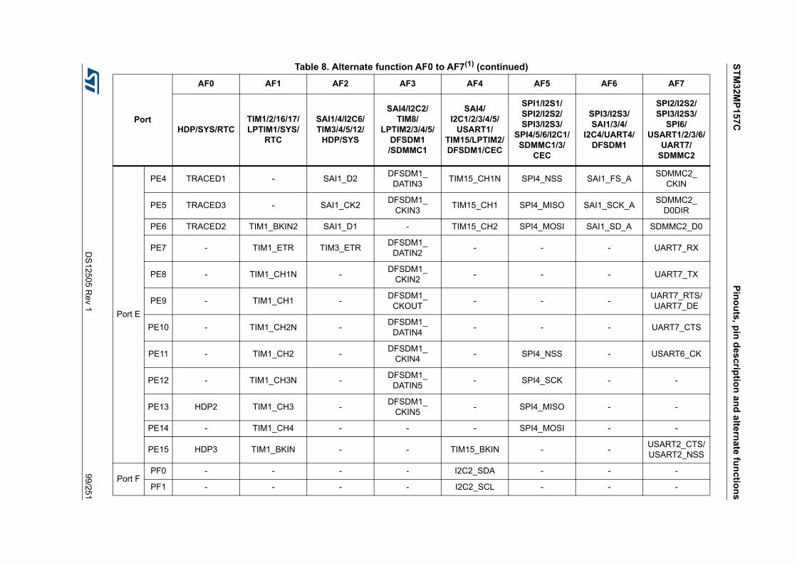
ST
M3
2MP
157
CP
ino
uts
, pin
des
criptio
n a
nd
alte
rna
te fu
nc
tion
s
DS
1250
5 Rev 1
99/251
Port E
PE4 TRACED1 - SAI1_D2DFSDM1_
DATIN3TIM15_CH1N SPI4_NSS SAI1_FS_A
SDMMC2_CKIN
PE5 TRACED3 - SAI1_CK2DFSDM1_
CKIN3TIM15_CH1 SPI4_MISO SAI1_SCK_A
SDMMC2_D0DIR
PE6 TRACED2 TIM1_BKIN2 SAI1_D1 - TIM15_CH2 SPI4_MOSI SAI1_SD_A SDMMC2_D0
PE7 - TIM1_ETR TIM3_ETRDFSDM1_
DATIN2- - - UART7_RX
PE8 - TIM1_CH1N -DFSDM1_
CKIN2- - - UART7_TX
PE9 - TIM1_CH1 -DFSDM1_
CKOUT- - -
UART7_RTS/UART7_DE
PE10 - TIM1_CH2N -DFSDM1_
DATIN4- - - UART7_CTS
PE11 - TIM1_CH2 -DFSDM1_
CKIN4- SPI4_NSS - USART6_CK
PE12 - TIM1_CH3N -DFSDM1_
DATIN5- SPI4_SCK - -
PE13 HDP2 TIM1_CH3 -DFSDM1_
CKIN5- SPI4_MISO - -
PE14 - TIM1_CH4 - - - SPI4_MOSI - -
PE15 HDP3 TIM1_BKIN - - TIM15_BKIN - -USART2_CTS/USART2_NSS
Port FPF0 - - - - I2C2_SDA - - -
PF1 - - - - I2C2_SCL - - -
Table 8. Alternate function AF0 to AF7(1) (continued)
Port
AF0 AF1 AF2 AF3 AF4 AF5 AF6 AF7
HDP/SYS/RTCTIM1/2/16/17/LPTIM1/SYS/
RTC
SAI1/4/I2C6/TIM3/4/5/12/
HDP/SYS
SAI4/I2C2/TIM8/
LPTIM2/3/4/5/DFSDM1/SDMMC1
SAI4/I2C1/2/3/4/5/
USART1/TIM15/LPTIM2/DFSDM1/CEC
SPI1/I2S1/SPI2/I2S2/SPI3/I2S3/
SPI4/5/6/I2C1/SDMMC1/3/
CEC
SPI3/I2S3/SAI1/3/4/
I2C4/UART4/DFSDM1
SPI2/I2S2/SPI3/I2S3/
SPI6/USART1/2/3/6/
UART7/SDMMC2

Pin
ou
ts, p
in d
esc
riptio
n a
nd
altern
ate
fun
ctio
ns
ST
M3
2M
P15
7C
100/251
DS
1250
5 Rev 1
Port F
PF2 - - - - I2C2_SMBA - - -
PF3 - - - - - - - -
PF4 - - - - - - - USART2_RX
PF5 - - - - - - - USART2_TX
PF6 - TIM16_CH1 - - - SPI5_NSS SAI1_SD_B UART7_RX
PF7 - TIM17_CH1 - - - SPI5_SCK SAI1_MCLK_B UART7_TX
PF8 TRACED12 TIM16_CH1N - - - SPI5_MISO SAI1_SCK_BUART7_RTS/UART7_DE
PF9 TRACED13 TIM17_CH1N - - - SPI5_MOSI SAI1_FS_B UART7_CTS
PF10 - TIM16_BKIN SAI1_D3 SAI4_D4 - - SAI1_D4 -
PF11 - - - - - SPI5_MOSI - -
PF12 TRACED4 - - - - - - -
PF13 TRACED5 - -DFSDM1_
DATIN6I2C4_SMBA I2C1_SMBA
DFSDM1_DATIN3
-
PF14 TRACED6 - -DFSDM1_
CKIN6I2C4_SCL I2C1_SCL - -
PF15 TRACED7 - - - I2C4_SDA I2C1_SDA - -
Port G
PG0 TRACED0 - -DFSDM1_
DATIN0- - - -
PG1 TRACED1 - - - - - - -
PG2 TRACED2 MCO2 - TIM8_BKIN - - - -
Table 8. Alternate function AF0 to AF7(1) (continued)
Port
AF0 AF1 AF2 AF3 AF4 AF5 AF6 AF7
HDP/SYS/RTCTIM1/2/16/17/LPTIM1/SYS/
RTC
SAI1/4/I2C6/TIM3/4/5/12/
HDP/SYS
SAI4/I2C2/TIM8/
LPTIM2/3/4/5/DFSDM1/SDMMC1
SAI4/I2C1/2/3/4/5/
USART1/TIM15/LPTIM2/DFSDM1/CEC
SPI1/I2S1/SPI2/I2S2/SPI3/I2S3/
SPI4/5/6/I2C1/SDMMC1/3/
CEC
SPI3/I2S3/SAI1/3/4/
I2C4/UART4/DFSDM1
SPI2/I2S2/SPI3/I2S3/
SPI6/USART1/2/3/6/
UART7/SDMMC2
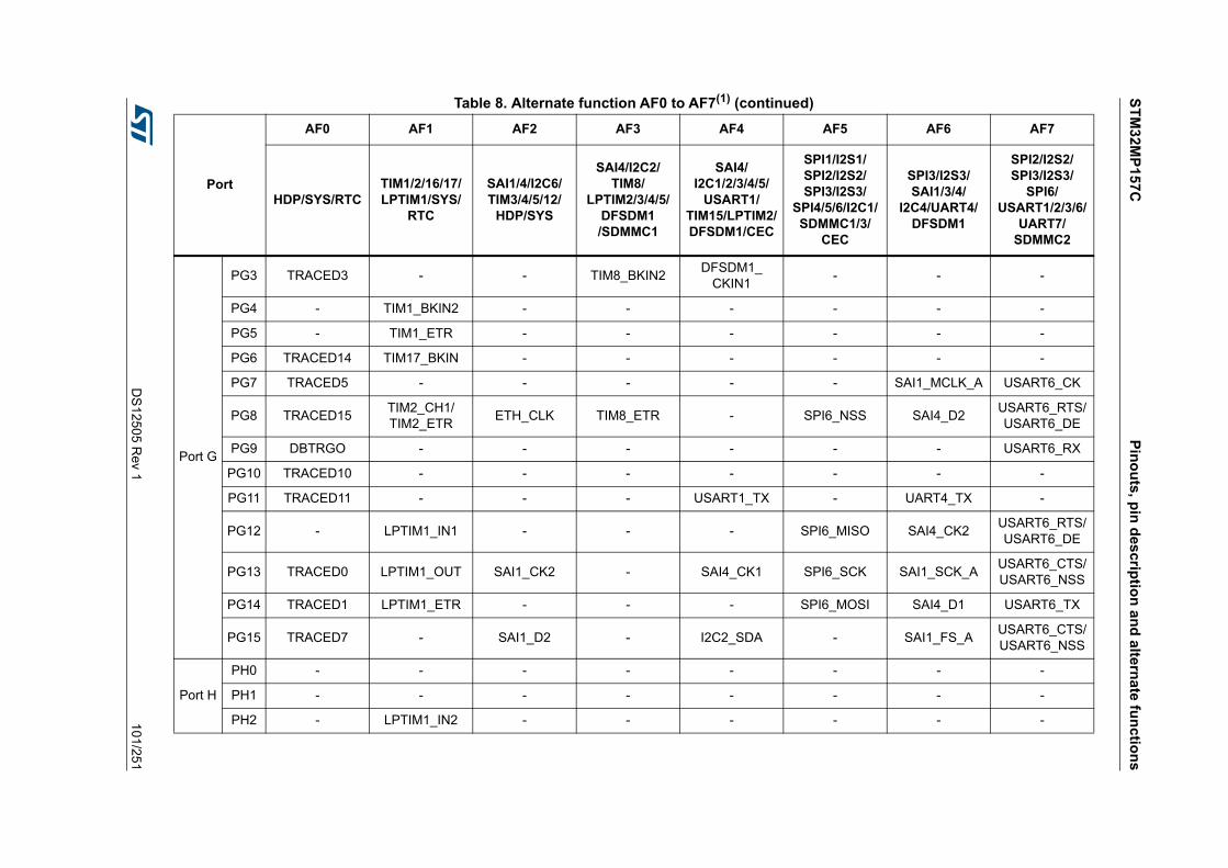
ST
M3
2MP
157
CP
ino
uts
, pin
des
criptio
n a
nd
alte
rna
te fu
nc
tion
s
DS
1250
5 Rev 1
101/251
Port G
PG3 TRACED3 - - TIM8_BKIN2DFSDM1_
CKIN1- - -
PG4 - TIM1_BKIN2 - - - - - -
PG5 - TIM1_ETR - - - - - -
PG6 TRACED14 TIM17_BKIN - - - - - -
PG7 TRACED5 - - - - - SAI1_MCLK_A USART6_CK
PG8 TRACED15TIM2_CH1/TIM2_ETR
ETH_CLK TIM8_ETR - SPI6_NSS SAI4_D2USART6_RTS/USART6_DE
PG9 DBTRGO - - - - - - USART6_RX
PG10 TRACED10 - - - - - - -
PG11 TRACED11 - - - USART1_TX - UART4_TX -
PG12 - LPTIM1_IN1 - - - SPI6_MISO SAI4_CK2USART6_RTS/USART6_DE
PG13 TRACED0 LPTIM1_OUT SAI1_CK2 - SAI4_CK1 SPI6_SCK SAI1_SCK_AUSART6_CTS/USART6_NSS
PG14 TRACED1 LPTIM1_ETR - - - SPI6_MOSI SAI4_D1 USART6_TX
PG15 TRACED7 - SAI1_D2 - I2C2_SDA - SAI1_FS_AUSART6_CTS/USART6_NSS
Port H
PH0 - - - - - - - -
PH1 - - - - - - - -
PH2 - LPTIM1_IN2 - - - - - -
Table 8. Alternate function AF0 to AF7(1) (continued)
Port
AF0 AF1 AF2 AF3 AF4 AF5 AF6 AF7
HDP/SYS/RTCTIM1/2/16/17/LPTIM1/SYS/
RTC
SAI1/4/I2C6/TIM3/4/5/12/
HDP/SYS
SAI4/I2C2/TIM8/
LPTIM2/3/4/5/DFSDM1/SDMMC1
SAI4/I2C1/2/3/4/5/
USART1/TIM15/LPTIM2/DFSDM1/CEC
SPI1/I2S1/SPI2/I2S2/SPI3/I2S3/
SPI4/5/6/I2C1/SDMMC1/3/
CEC
SPI3/I2S3/SAI1/3/4/
I2C4/UART4/DFSDM1
SPI2/I2S2/SPI3/I2S3/
SPI6/USART1/2/3/6/
UART7/SDMMC2
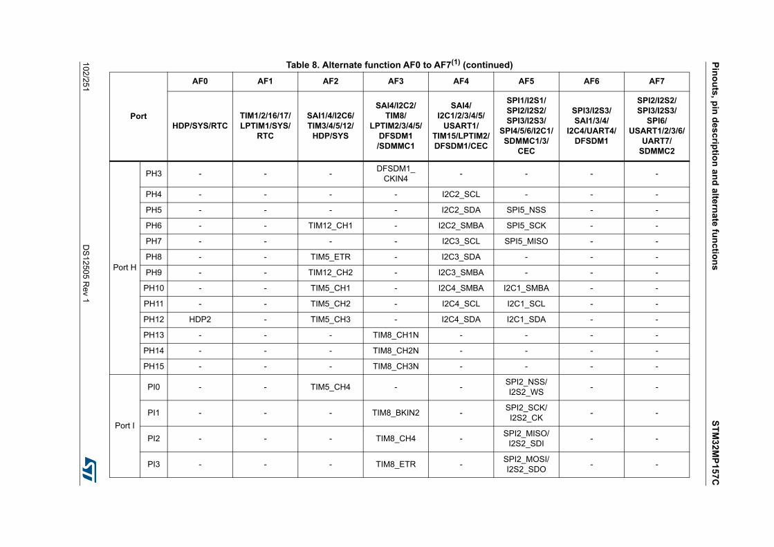
Pin
ou
ts, p
in d
esc
riptio
n a
nd
altern
ate
fun
ctio
ns
ST
M3
2M
P15
7C
102/251
DS
1250
5 Rev 1
Port H
PH3 - - -DFSDM1_
CKIN4- - - -
PH4 - - - - I2C2_SCL - - -
PH5 - - - - I2C2_SDA SPI5_NSS - -
PH6 - - TIM12_CH1 - I2C2_SMBA SPI5_SCK - -
PH7 - - - - I2C3_SCL SPI5_MISO - -
PH8 - - TIM5_ETR - I2C3_SDA - - -
PH9 - - TIM12_CH2 - I2C3_SMBA - - -
PH10 - - TIM5_CH1 - I2C4_SMBA I2C1_SMBA - -
PH11 - - TIM5_CH2 - I2C4_SCL I2C1_SCL - -
PH12 HDP2 - TIM5_CH3 - I2C4_SDA I2C1_SDA - -
PH13 - - - TIM8_CH1N - - - -
PH14 - - - TIM8_CH2N - - - -
PH15 - - - TIM8_CH3N - - - -
Port I
PI0 - - TIM5_CH4 - -SPI2_NSS/I2S2_WS
- -
PI1 - - - TIM8_BKIN2 -SPI2_SCK/I2S2_CK
- -
PI2 - - - TIM8_CH4 -SPI2_MISO/
I2S2_SDI- -
PI3 - - - TIM8_ETR -SPI2_MOSI/I2S2_SDO
- -
Table 8. Alternate function AF0 to AF7(1) (continued)
Port
AF0 AF1 AF2 AF3 AF4 AF5 AF6 AF7
HDP/SYS/RTCTIM1/2/16/17/LPTIM1/SYS/
RTC
SAI1/4/I2C6/TIM3/4/5/12/
HDP/SYS
SAI4/I2C2/TIM8/
LPTIM2/3/4/5/DFSDM1/SDMMC1
SAI4/I2C1/2/3/4/5/
USART1/TIM15/LPTIM2/DFSDM1/CEC
SPI1/I2S1/SPI2/I2S2/SPI3/I2S3/
SPI4/5/6/I2C1/SDMMC1/3/
CEC
SPI3/I2S3/SAI1/3/4/
I2C4/UART4/DFSDM1
SPI2/I2S2/SPI3/I2S3/
SPI6/USART1/2/3/6/
UART7/SDMMC2

ST
M3
2MP
157
CP
ino
uts
, pin
des
criptio
n a
nd
alte
rna
te fu
nc
tion
s
DS
1250
5 Rev 1
103/251
Port I
PI4 - - - TIM8_BKIN - - - -
PI5 - - - TIM8_CH1 - - - -
PI6 - - - TIM8_CH2 - - - -
PI7 - - - TIM8_CH3 - - - -
PI8 - - - - - - - -
PI9 HDP1 - - - - - - -
PI10 HDP0 - - - - - - -
PI11 MCO1 - - - - I2S_CKIN - -
PI12 TRACED0 - HDP0 - - - - -
PI13 TRACED1 - HDP1 - - - - -
PI14 TRACECLK - - - - - - -
PI15 - - - - - - - -
Port J
PJ0 TRACED8 - - - - - - -
PJ1 TRACED9 - - - - - - -
PJ2 TRACED10 - - - - - - -
PJ3 TRACED11 - - - - - - -
PJ4 TRACED12 - - - - - - -
PJ5 TRACED2 - HDP2 - - - - -
PJ6 TRACED3 - HDP3 TIM8_CH2 - - - -
PJ7 TRACED13 - - TIM8_CH2N - - - -
Table 8. Alternate function AF0 to AF7(1) (continued)
Port
AF0 AF1 AF2 AF3 AF4 AF5 AF6 AF7
HDP/SYS/RTCTIM1/2/16/17/LPTIM1/SYS/
RTC
SAI1/4/I2C6/TIM3/4/5/12/
HDP/SYS
SAI4/I2C2/TIM8/
LPTIM2/3/4/5/DFSDM1/SDMMC1
SAI4/I2C1/2/3/4/5/
USART1/TIM15/LPTIM2/DFSDM1/CEC
SPI1/I2S1/SPI2/I2S2/SPI3/I2S3/
SPI4/5/6/I2C1/SDMMC1/3/
CEC
SPI3/I2S3/SAI1/3/4/
I2C4/UART4/DFSDM1
SPI2/I2S2/SPI3/I2S3/
SPI6/USART1/2/3/6/
UART7/SDMMC2

Pin
ou
ts, p
in d
esc
riptio
n a
nd
altern
ate
fun
ctio
ns
ST
M3
2M
P15
7C
104/251
DS
1250
5 Rev 1
Port J
PJ8 TRACED14 TIM1_CH3N - TIM8_CH1 - - - -
PJ9 TRACED15 TIM1_CH3 - TIM8_CH1N - - - -
PJ10 - TIM1_CH2N - TIM8_CH2 - SPI5_MOSI - -
PJ11 - TIM1_CH2 - TIM8_CH2N - SPI5_MISO - -
PJ12 - - - - - - - -
PJ13 - - - - - - - -
PJ14 - - - - - - - -
PJ15 - - - - - - - -
Port K
PK0 - TIM1_CH1N - TIM8_CH3 - SPI5_SCK - -
PK1 TRACED4 TIM1_CH1 HDP4 TIM8_CH3N - SPI5_NSS - -
PK2 TRACED5 TIM1_BKIN HDP5 TIM8_BKIN - - - -
PK3 - - - - - - - -
PK4 - - - - - - - -
PK5 TRACED6 - HDP6 - - - - -
PK6 TRACED7 - HDP7 - - - - -
PK7 - - - - - - - -
Port Z
PZ0 - - I2C6_SCL I2C2_SCL -SPI1_SCK/I2S1_CK
- USART1_CK
PZ1 - - I2C6_SDA I2C2_SDA I2C5_SDASPI1_MISO/
I2S1_SDII2C4_SDA USART1_RX
Table 8. Alternate function AF0 to AF7(1) (continued)
Port
AF0 AF1 AF2 AF3 AF4 AF5 AF6 AF7
HDP/SYS/RTCTIM1/2/16/17/LPTIM1/SYS/
RTC
SAI1/4/I2C6/TIM3/4/5/12/
HDP/SYS
SAI4/I2C2/TIM8/
LPTIM2/3/4/5/DFSDM1/SDMMC1
SAI4/I2C1/2/3/4/5/
USART1/TIM15/LPTIM2/DFSDM1/CEC
SPI1/I2S1/SPI2/I2S2/SPI3/I2S3/
SPI4/5/6/I2C1/SDMMC1/3/
CEC
SPI3/I2S3/SAI1/3/4/
I2C4/UART4/DFSDM1
SPI2/I2S2/SPI3/I2S3/
SPI6/USART1/2/3/6/
UART7/SDMMC2
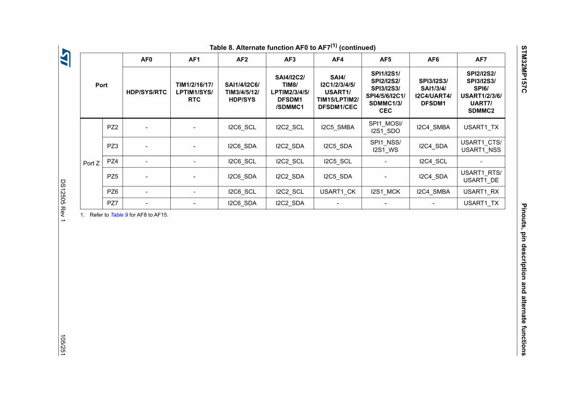
ST
M3
2MP
157
CP
ino
uts
, pin
des
criptio
n a
nd
alte
rna
te fu
nc
tion
s
DS
1250
5 Rev 1
105/251
Port Z
PZ2 - - I2C6_SCL I2C2_SCL I2C5_SMBASPI1_MOSI/I2S1_SDO
I2C4_SMBA USART1_TX
PZ3 - - I2C6_SDA I2C2_SDA I2C5_SDASPI1_NSS/I2S1_WS
I2C4_SDAUSART1_CTS/USART1_NSS
PZ4 - - I2C6_SCL I2C2_SCL I2C5_SCL - I2C4_SCL -
PZ5 - - I2C6_SDA I2C2_SDA I2C5_SDA - I2C4_SDAUSART1_RTS/USART1_DE
PZ6 - - I2C6_SCL I2C2_SCL USART1_CK I2S1_MCK I2C4_SMBA USART1_RX
PZ7 - - I2C6_SDA I2C2_SDA - - - USART1_TX
1. Refer to Table 9 for AF8 to AF15.
Table 8. Alternate function AF0 to AF7(1) (continued)
Port
AF0 AF1 AF2 AF3 AF4 AF5 AF6 AF7
HDP/SYS/RTCTIM1/2/16/17/LPTIM1/SYS/
RTC
SAI1/4/I2C6/TIM3/4/5/12/
HDP/SYS
SAI4/I2C2/TIM8/
LPTIM2/3/4/5/DFSDM1/SDMMC1
SAI4/I2C1/2/3/4/5/
USART1/TIM15/LPTIM2/DFSDM1/CEC
SPI1/I2S1/SPI2/I2S2/SPI3/I2S3/
SPI4/5/6/I2C1/SDMMC1/3/
CEC
SPI3/I2S3/SAI1/3/4/
I2C4/UART4/DFSDM1
SPI2/I2S2/SPI3/I2S3/
SPI6/USART1/2/3/6/
UART7/SDMMC2
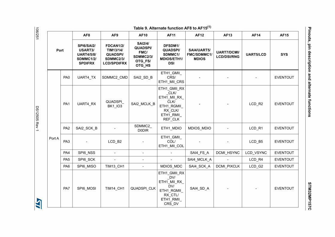
Pin
ou
ts, p
in d
esc
riptio
n a
nd
altern
ate
fun
ctio
ns
ST
M3
2M
P15
7C
106/251
DS
1250
5 Rev 1
Table 9. Alternate function AF8 to AF15(1)
Port
AF8 AF9 AF10 AF11 AF12 AF13 AF14 AF15
SPI6/SAI2/USART3/
UART4/5/8/SDMMC1/2/SPDIFRX
FDCAN1/2/TIM13/14/QUADSPI/
SDMMC2/3/LCD/SPDIFRX
SAI2/4/QUADSPI/
FMC/SDMMC2/3/
OTG_FS/OTG_HS
DFSDM1/QUADSPI/SDMMC1/
MDIOS/ETH1/DSI
SAI4/UART5/FMC/SDMMC1/
MDIOS
UART7/DCMI/LCD/DSI/RNG
UART5/LCD SYS
Port A
PA0 UART4_TX SDMMC2_CMD SAI2_SD_BETH1_GMII_
CRS/ETH1_MII_CRS
- - - EVENTOUT
PA1 UART4_RXQUADSPI_BK1_IO3
SAI2_MCLK_B
ETH1_GMII_RX_CLK/
ETH1_MII_RX_CLK/
ETH1_RGMII_RX_CLK/
ETH1_RMII_REF_CLK
- - LCD_R2 EVENTOUT
PA2 SAI2_SCK_B -SDMMC2_
D0DIRETH1_MDIO MDIOS_MDIO - LCD_R1 EVENTOUT
PA3 - LCD_B2 -ETH1_GMII_
COL/ETH1_MII_COL
- - LCD_B5 EVENTOUT
PA4 SPI6_NSS - - - SAI4_FS_A DCMI_HSYNC LCD_VSYNC EVENTOUT
PA5 SPI6_SCK - - - SAI4_MCLK_A - LCD_R4 EVENTOUT
PA6 SPI6_MISO TIM13_CH1 - MDIOS_MDC SAI4_SCK_A DCMI_PIXCLK LCD_G2 EVENTOUT
PA7 SPI6_MOSI TIM14_CH1 QUADSPI_CLK
ETH1_GMII_RX_DV/
ETH1_MII_RX_DV/
ETH1_RGMII_RX_CTL/
ETH1_RMII_CRS_DV
SAI4_SD_A - - EVENTOUT

ST
M3
2MP
157
CP
ino
uts
, pin
des
criptio
n a
nd
alte
rna
te fu
nc
tion
s
DS
1250
5 Rev 1
107/251
Port A
PA8SDMMC2_
CKINSDMMC2_D4
OTG_FS_SOF/OTG_HS_SOF
- SAI4_SD_B UART7_RX LCD_R6 EVENTOUT
PA9SDMMC2_
CDIR- SDMMC2_D5 - - DCMI_D0 LCD_R5 EVENTOUT
PA10 - - - MDIOS_MDIO SAI4_FS_B DCMI_D1 LCD_B1 EVENTOUT
PA11 - FDCAN1_RX - - - - LCD_R4 EVENTOUT
PA12 SAI2_FS_B FDCAN1_TX - - - - LCD_R5 EVENTOUT
PA13 UART4_TX - - - - - - EVENTOUT
PA14 - - - - - - - EVENTOUT
PA15UART4_RTS/UART4_DE
SDMMC2_D5SDMMC2_
CDIRSDMMC1_D5 SAI4_FS_A UART7_TX LCD_R1 EVENTOUT
Port B
PB0 UART4_CTS LCD_R3 -
ETH1_GMII_RXD2/
ETH1_MII_RXD2/
ETH1_RGMII_RXD2
MDIOS_MDIO - LCD_G1 EVENTOUT
PB1 - LCD_R6 -
ETH1_GMII_RXD3/
ETH1_MII_RXD3/
ETH1_RGMII_RXD3
MDIOS_MDC - LCD_G0 EVENTOUT
PB2 UART4_RX QUADSPI_CLK - - - - - EVENTOUT
PB3 SPI6_SCK SDMMC2_D2 - - SAI4_MCLK_A UART7_RX - EVENTOUT
Table 9. Alternate function AF8 to AF15(1) (continued)
Port
AF8 AF9 AF10 AF11 AF12 AF13 AF14 AF15
SPI6/SAI2/USART3/
UART4/5/8/SDMMC1/2/SPDIFRX
FDCAN1/2/TIM13/14/QUADSPI/
SDMMC2/3/LCD/SPDIFRX
SAI2/4/QUADSPI/
FMC/SDMMC2/3/
OTG_FS/OTG_HS
DFSDM1/QUADSPI/SDMMC1/
MDIOS/ETH1/DSI
SAI4/UART5/FMC/SDMMC1/
MDIOS
UART7/DCMI/LCD/DSI/RNG
UART5/LCD SYS

Pin
ou
ts, p
in d
esc
riptio
n a
nd
altern
ate
fun
ctio
ns
ST
M3
2M
P15
7C
108/251
DS
1250
5 Rev 1
Port B
PB4 SPI6_MISO SDMMC2_D3 - - SAI4_SCK_A UART7_TX - EVENTOUT
PB5 SPI6_MOSI FDCAN2_RX SAI4_SD_AETH1_PPS_
OUTUART5_RX DCMI_D10 LCD_G7 EVENTOUT
PB6 - FDCAN2_TXQUADSPI_BK1
_NCSDFSDM1_
DATIN5UART5_TX DCMI_D5 - EVENTOUT
PB7 - - SDMMC2_D1DFSDM1_
CKIN5FMC_NL DCMI_VSYNC - EVENTOUT
PB8 UART4_RX FDCAN1_RX SDMMC2_D4
ETH1_GMII_TXD3/
ETH1_MII_TXD3/
ETH1_RGMII_TXD3
SDMMC1_D4 DCMI_D6 LCD_B6 EVENTOUT
PB9 UART4_TX FDCAN1_TX SDMMC2_D5SDMMC1_CDI
RSDMMC1_D5 DCMI_D7 LCD_B7 EVENTOUT
PB10 -QUADSPI_BK1_NCS
-
ETH1_GMII_RX_ER/
ETH1_MII_RX_ER
- - LCD_G4 EVENTOUT
PB11 - - -
ETH1_GMII_TX_EN/
ETH1_MII_TX_EN/
ETH1_RGMII_TX_CTL/
ETH1_RMII_TX_EN
- DSI_TE LCD_G5 EVENTOUT
Table 9. Alternate function AF8 to AF15(1) (continued)
Port
AF8 AF9 AF10 AF11 AF12 AF13 AF14 AF15
SPI6/SAI2/USART3/
UART4/5/8/SDMMC1/2/SPDIFRX
FDCAN1/2/TIM13/14/QUADSPI/
SDMMC2/3/LCD/SPDIFRX
SAI2/4/QUADSPI/
FMC/SDMMC2/3/
OTG_FS/OTG_HS
DFSDM1/QUADSPI/SDMMC1/
MDIOS/ETH1/DSI
SAI4/UART5/FMC/SDMMC1/
MDIOS
UART7/DCMI/LCD/DSI/RNG
UART5/LCD SYS
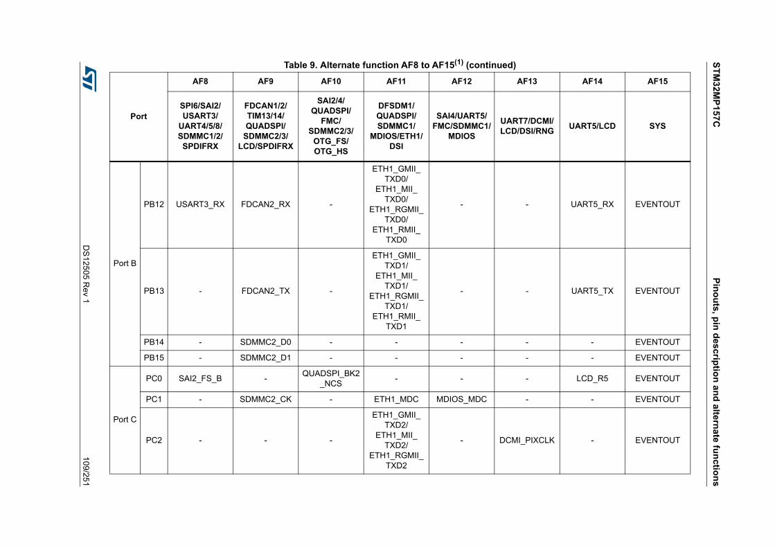
ST
M3
2MP
157
CP
ino
uts
, pin
des
criptio
n a
nd
alte
rna
te fu
nc
tion
s
DS
1250
5 Rev 1
109/251
Port B
PB12 USART3_RX FDCAN2_RX -
ETH1_GMII_TXD0/
ETH1_MII_TXD0/
ETH1_RGMII_TXD0/
ETH1_RMII_TXD0
- - UART5_RX EVENTOUT
PB13 - FDCAN2_TX -
ETH1_GMII_TXD1/
ETH1_MII_TXD1/
ETH1_RGMII_TXD1/
ETH1_RMII_TXD1
- - UART5_TX EVENTOUT
PB14 - SDMMC2_D0 - - - - - EVENTOUT
PB15 - SDMMC2_D1 - - - - - EVENTOUT
Port C
PC0 SAI2_FS_B -QUADSPI_BK2
_NCS- - - LCD_R5 EVENTOUT
PC1 - SDMMC2_CK - ETH1_MDC MDIOS_MDC - - EVENTOUT
PC2 - - -
ETH1_GMII_TXD2/
ETH1_MII_TXD2/
ETH1_RGMII_TXD2
- DCMI_PIXCLK - EVENTOUT
Table 9. Alternate function AF8 to AF15(1) (continued)
Port
AF8 AF9 AF10 AF11 AF12 AF13 AF14 AF15
SPI6/SAI2/USART3/
UART4/5/8/SDMMC1/2/SPDIFRX
FDCAN1/2/TIM13/14/QUADSPI/
SDMMC2/3/LCD/SPDIFRX
SAI2/4/QUADSPI/
FMC/SDMMC2/3/
OTG_FS/OTG_HS
DFSDM1/QUADSPI/SDMMC1/
MDIOS/ETH1/DSI
SAI4/UART5/FMC/SDMMC1/
MDIOS
UART7/DCMI/LCD/DSI/RNG
UART5/LCD SYS
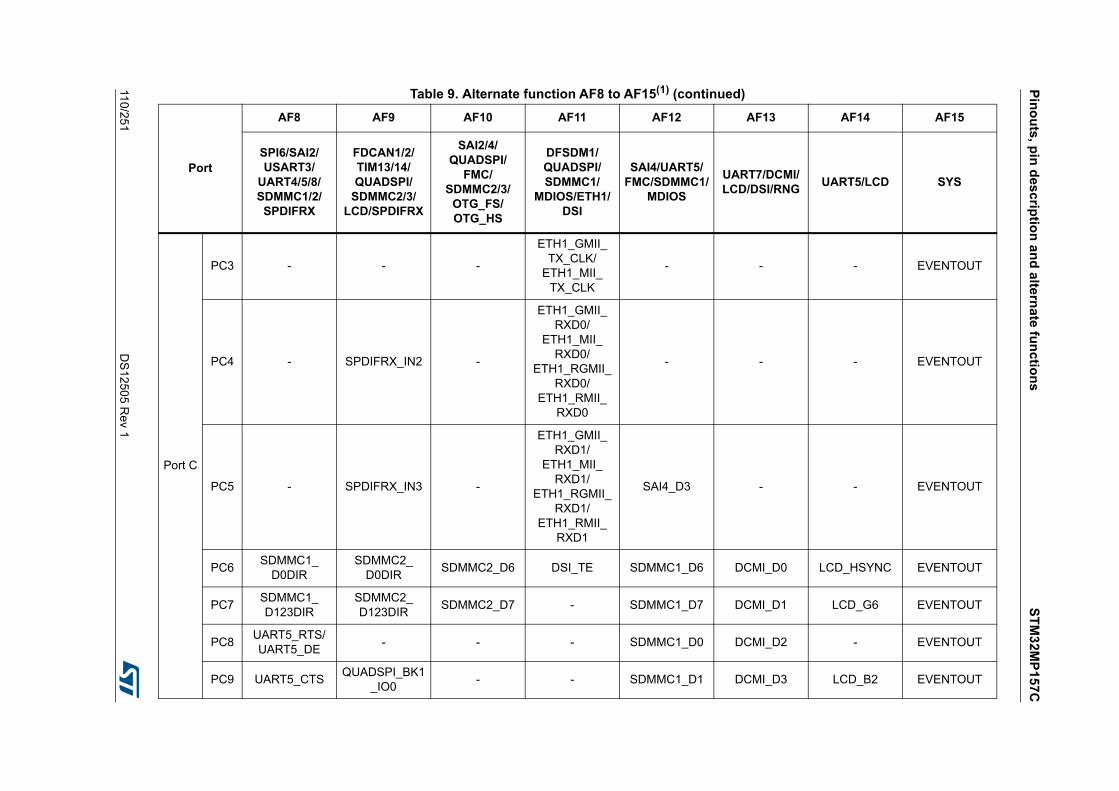
Pin
ou
ts, p
in d
esc
riptio
n a
nd
altern
ate
fun
ctio
ns
ST
M3
2M
P15
7C
110/251
DS
1250
5 Rev 1
Port C
PC3 - - -
ETH1_GMII_TX_CLK/
ETH1_MII_TX_CLK
- - - EVENTOUT
PC4 - SPDIFRX_IN2 -
ETH1_GMII_RXD0/
ETH1_MII_RXD0/
ETH1_RGMII_RXD0/
ETH1_RMII_RXD0
- - - EVENTOUT
PC5 - SPDIFRX_IN3 -
ETH1_GMII_RXD1/
ETH1_MII_RXD1/
ETH1_RGMII_RXD1/
ETH1_RMII_RXD1
SAI4_D3 - - EVENTOUT
PC6SDMMC1_
D0DIRSDMMC2_
D0DIRSDMMC2_D6 DSI_TE SDMMC1_D6 DCMI_D0 LCD_HSYNC EVENTOUT
PC7SDMMC1_D123DIR
SDMMC2_D123DIR
SDMMC2_D7 - SDMMC1_D7 DCMI_D1 LCD_G6 EVENTOUT
PC8UART5_RTS/UART5_DE
- - - SDMMC1_D0 DCMI_D2 - EVENTOUT
PC9 UART5_CTSQUADSPI_BK1
_IO0- - SDMMC1_D1 DCMI_D3 LCD_B2 EVENTOUT
Table 9. Alternate function AF8 to AF15(1) (continued)
Port
AF8 AF9 AF10 AF11 AF12 AF13 AF14 AF15
SPI6/SAI2/USART3/
UART4/5/8/SDMMC1/2/SPDIFRX
FDCAN1/2/TIM13/14/QUADSPI/
SDMMC2/3/LCD/SPDIFRX
SAI2/4/QUADSPI/
FMC/SDMMC2/3/
OTG_FS/OTG_HS
DFSDM1/QUADSPI/SDMMC1/
MDIOS/ETH1/DSI
SAI4/UART5/FMC/SDMMC1/
MDIOS
UART7/DCMI/LCD/DSI/RNG
UART5/LCD SYS

ST
M3
2MP
157
CP
ino
uts
, pin
des
criptio
n a
nd
alte
rna
te fu
nc
tion
s
DS
1250
5 Rev 1
111/251
Port C
PC10 UART4_TXQUADSPI_BK1_IO1
SAI4_MCLK_B - SDMMC1_D2 DCMI_D8 LCD_R2 EVENTOUT
PC11 UART4_RXQUADSPI_BK2_NCS
SAI4_SCK_B - SDMMC1_D3 DCMI_D4 - EVENTOUT
PC12 UART5_TX - SAI4_SD_B - SDMMC1_CK DCMI_D9 - EVENTOUT
PC13 - - - - - - - EVENTOUT
PC14 - - - - - - - EVENTOUT
PC15 - - - - - - - EVENTOUT
Table 9. Alternate function AF8 to AF15(1) (continued)
Port
AF8 AF9 AF10 AF11 AF12 AF13 AF14 AF15
SPI6/SAI2/USART3/
UART4/5/8/SDMMC1/2/SPDIFRX
FDCAN1/2/TIM13/14/QUADSPI/
SDMMC2/3/LCD/SPDIFRX
SAI2/4/QUADSPI/
FMC/SDMMC2/3/
OTG_FS/OTG_HS
DFSDM1/QUADSPI/SDMMC1/
MDIOS/ETH1/DSI
SAI4/UART5/FMC/SDMMC1/
MDIOS
UART7/DCMI/LCD/DSI/RNG
UART5/LCD SYS
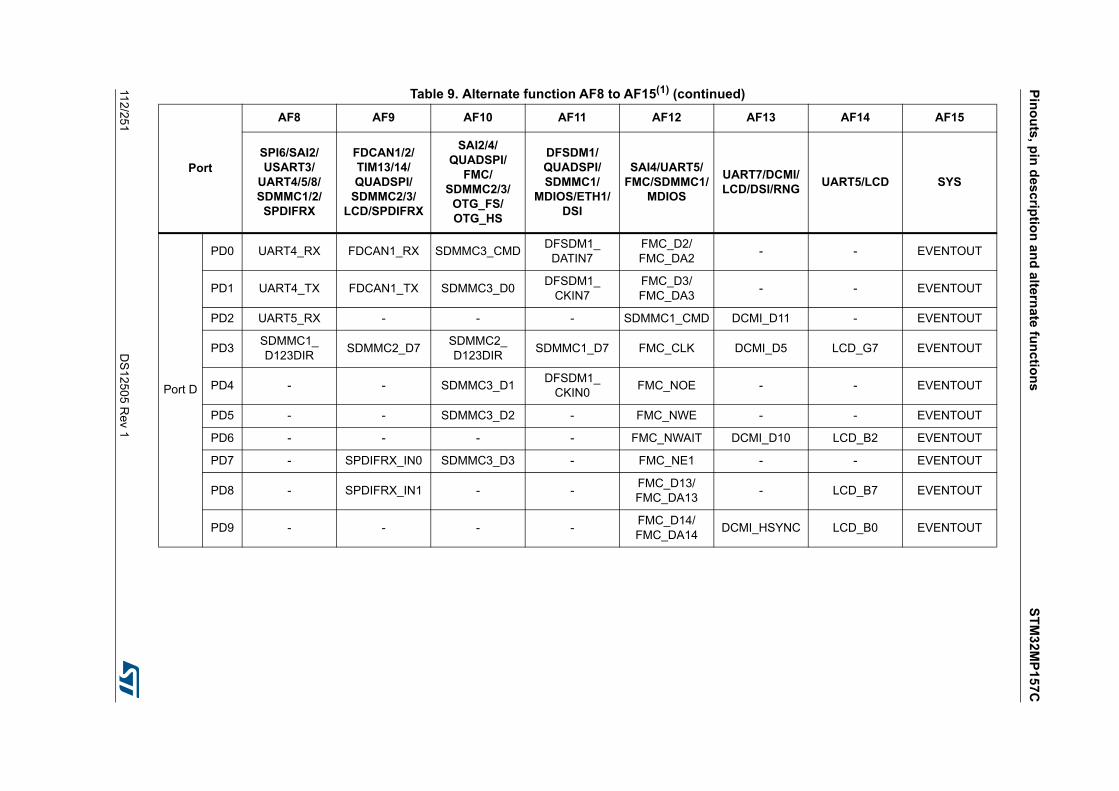
Pin
ou
ts, p
in d
esc
riptio
n a
nd
altern
ate
fun
ctio
ns
ST
M3
2M
P15
7C
112/251
DS
1250
5 Rev 1
Port D
PD0 UART4_RX FDCAN1_RX SDMMC3_CMDDFSDM1_
DATIN7FMC_D2/FMC_DA2
- - EVENTOUT
PD1 UART4_TX FDCAN1_TX SDMMC3_D0DFSDM1_
CKIN7FMC_D3/FMC_DA3
- - EVENTOUT
PD2 UART5_RX - - - SDMMC1_CMD DCMI_D11 - EVENTOUT
PD3SDMMC1_D123DIR
SDMMC2_D7SDMMC2_D123DIR
SDMMC1_D7 FMC_CLK DCMI_D5 LCD_G7 EVENTOUT
PD4 - - SDMMC3_D1DFSDM1_
CKIN0FMC_NOE - - EVENTOUT
PD5 - - SDMMC3_D2 - FMC_NWE - - EVENTOUT
PD6 - - - - FMC_NWAIT DCMI_D10 LCD_B2 EVENTOUT
PD7 - SPDIFRX_IN0 SDMMC3_D3 - FMC_NE1 - - EVENTOUT
PD8 - SPDIFRX_IN1 - -FMC_D13/FMC_DA13
- LCD_B7 EVENTOUT
PD9 - - - -FMC_D14/FMC_DA14
DCMI_HSYNC LCD_B0 EVENTOUT
Table 9. Alternate function AF8 to AF15(1) (continued)
Port
AF8 AF9 AF10 AF11 AF12 AF13 AF14 AF15
SPI6/SAI2/USART3/
UART4/5/8/SDMMC1/2/SPDIFRX
FDCAN1/2/TIM13/14/QUADSPI/
SDMMC2/3/LCD/SPDIFRX
SAI2/4/QUADSPI/
FMC/SDMMC2/3/
OTG_FS/OTG_HS
DFSDM1/QUADSPI/SDMMC1/
MDIOS/ETH1/DSI
SAI4/UART5/FMC/SDMMC1/
MDIOS
UART7/DCMI/LCD/DSI/RNG
UART5/LCD SYS
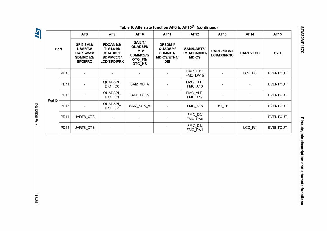
ST
M3
2MP
157
CP
ino
uts
, pin
des
criptio
n a
nd
alte
rna
te fu
nc
tion
s
DS
1250
5 Rev 1
113/251
Port D
PD10 - - - -FMC_D15/FMC_DA15
- LCD_B3 EVENTOUT
PD11 -QUADSPI_BK1_IO0
SAI2_SD_A -FMC_CLE/FMC_A16
- - EVENTOUT
PD12 -QUADSPI_BK1_IO1
SAI2_FS_A -FMC_ALE/FMC_A17
- - EVENTOUT
PD13 -QUADSPI_BK1_IO3
SAI2_SCK_A - FMC_A18 DSI_TE - EVENTOUT
PD14 UART8_CTS - - -FMC_D0/FMC_DA0
- - EVENTOUT
PD15 UART8_CTS - - -FMC_D1/FMC_DA1
- LCD_R1 EVENTOUT
Table 9. Alternate function AF8 to AF15(1) (continued)
Port
AF8 AF9 AF10 AF11 AF12 AF13 AF14 AF15
SPI6/SAI2/USART3/
UART4/5/8/SDMMC1/2/SPDIFRX
FDCAN1/2/TIM13/14/QUADSPI/
SDMMC2/3/LCD/SPDIFRX
SAI2/4/QUADSPI/
FMC/SDMMC2/3/
OTG_FS/OTG_HS
DFSDM1/QUADSPI/SDMMC1/
MDIOS/ETH1/DSI
SAI4/UART5/FMC/SDMMC1/
MDIOS
UART7/DCMI/LCD/DSI/RNG
UART5/LCD SYS

Pin
ou
ts, p
in d
esc
riptio
n a
nd
altern
ate
fun
ctio
ns
ST
M3
2M
P15
7C
114/251
DS
1250
5 Rev 1
Port E
PE0 UART8_RX - SAI2_MCLK_A - FMC_NBL0 DCMI_D2 - EVENTOUT
PE1 UART8_TX - - - FMC_NBL1 DCMI_D3 - EVENTOUT
PE2 -QUADSPI_BK1_IO2
-
ETH1_GMII_TXD3/
ETH1_MII_TXD3/
ETH1_RGMII_TXD3
FMC_A23 - - EVENTOUT
PE3 - SDMMC2_CK - - FMC_A19 - - EVENTOUT
PE4SDMMC1_
CKINSDMMC2_D4 - SDMMC1_D4 FMC_A20 DCMI_D4 LCD_B0 EVENTOUT
PE5SDMMC1_
D0DIRSDMMC2_D6 - SDMMC1_D6 FMC_A21 DCMI_D6 LCD_G0 EVENTOUT
PE6 SDMMC1_D2 - SAI2_MCLK_B - FMC_A22 DCMI_D7 LCD_G1 EVENTOUT
Table 9. Alternate function AF8 to AF15(1) (continued)
Port
AF8 AF9 AF10 AF11 AF12 AF13 AF14 AF15
SPI6/SAI2/USART3/
UART4/5/8/SDMMC1/2/SPDIFRX
FDCAN1/2/TIM13/14/QUADSPI/
SDMMC2/3/LCD/SPDIFRX
SAI2/4/QUADSPI/
FMC/SDMMC2/3/
OTG_FS/OTG_HS
DFSDM1/QUADSPI/SDMMC1/
MDIOS/ETH1/DSI
SAI4/UART5/FMC/SDMMC1/
MDIOS
UART7/DCMI/LCD/DSI/RNG
UART5/LCD SYS

ST
M3
2MP
157
CP
ino
uts
, pin
des
criptio
n a
nd
alte
rna
te fu
nc
tion
s
DS
1250
5 Rev 1
115/251
Port E
PE7 - -QUADSPI_BK2_IO0
-FMC_D4/FMC_DA4
- - EVENTOUT
PE8 - -QUADSPI_BK2_IO1
-FMC_D5/FMC_DA5
- - EVENTOUT
PE9 - -QUADSPI_BK2_IO2
-FMC_D6/FMC_DA6
- - EVENTOUT
PE10 - -QUADSPI_BK2_IO3
-FMC_D7/FMC_DA7
- - EVENTOUT
PE11 - - SAI2_SD_B -FMC_D8/FMC_DA8
DCMI_D4 LCD_G3 EVENTOUT
PE12SDMMC1_
D0DIR- SAI2_SCK_B -
FMC_D9/FMC_DA9
- LCD_B4 EVENTOUT
PE13 - - SAI2_FS_B -FMC_D10/FMC_DA10
DCMI_D6 LCD_DE EVENTOUT
PE14UART8_RTS/UART8_DE
- SAI2_MCLK_BSDMMC1_D123DIR
FMC_D11/FMC_DA11
LCD_G0 LCD_CLK EVENTOUT
PE15 UART8_CTS - FMC_NCE2 -FMC_D12/FMC_DA12
- LCD_R7 EVENTOUT
Port F
PF0 - SDMMC3_D0SDMMC3_
CKIN- FMC_A0 - - EVENTOUT
PF1 - SDMMC3_CMDSDMMC3_
CDIR- FMC_A1 - - EVENTOUT
PF2 -SDMMC2_
D0DIRSDMMC3_
D0DIRSDMMC1_
D0DIRFMC_A2 - - EVENTOUT
Table 9. Alternate function AF8 to AF15(1) (continued)
Port
AF8 AF9 AF10 AF11 AF12 AF13 AF14 AF15
SPI6/SAI2/USART3/
UART4/5/8/SDMMC1/2/SPDIFRX
FDCAN1/2/TIM13/14/QUADSPI/
SDMMC2/3/LCD/SPDIFRX
SAI2/4/QUADSPI/
FMC/SDMMC2/3/
OTG_FS/OTG_HS
DFSDM1/QUADSPI/SDMMC1/
MDIOS/ETH1/DSI
SAI4/UART5/FMC/SDMMC1/
MDIOS
UART7/DCMI/LCD/DSI/RNG
UART5/LCD SYS

Pin
ou
ts, p
in d
esc
riptio
n a
nd
altern
ate
fun
ctio
ns
ST
M3
2M
P15
7C
116/251
DS
1250
5 Rev 1
Port F
PF3 - - -
ETH1_GMII_TX_ER/
ETH1_MII_TX_ER
FMC_A3 - - EVENTOUT
PF4 - SDMMC3_D1SDMMC3_D123DIR
- FMC_A4 - - EVENTOUT
PF5 - SDMMC3_D2 - - FMC_A5 - - EVENTOUT
PF6 -QUADSPI_BK1_IO3
- - SAI4_SCK_B - - EVENTOUT
PF7 -QUADSPI_BK1_IO2
- - - - - EVENTOUT
PF8 - TIM13_CH1QUADSPI_BK1_IO0
- - - - EVENTOUT
PF9 - TIM14_CH1QUADSPI_BK1_IO1
- - - - EVENTOUT
PF10 - QUADSPI_CLK - - SAI4_D3 DCMI_D11 LCD_DE EVENTOUT
PF11 - - SAI2_SD_B - - DCMI_D12 LCD_G5 EVENTOUT
PF12 - - -ETH1_GMII_
RXD4FMC_A6 - - EVENTOUT
PF13 - - -ETH1_GMII_
RXD5FMC_A7 - - EVENTOUT
PF14 - - -ETH1_GMII_
RXD6FMC_A8 - - EVENTOUT
Table 9. Alternate function AF8 to AF15(1) (continued)
Port
AF8 AF9 AF10 AF11 AF12 AF13 AF14 AF15
SPI6/SAI2/USART3/
UART4/5/8/SDMMC1/2/SPDIFRX
FDCAN1/2/TIM13/14/QUADSPI/
SDMMC2/3/LCD/SPDIFRX
SAI2/4/QUADSPI/
FMC/SDMMC2/3/
OTG_FS/OTG_HS
DFSDM1/QUADSPI/SDMMC1/
MDIOS/ETH1/DSI
SAI4/UART5/FMC/SDMMC1/
MDIOS
UART7/DCMI/LCD/DSI/RNG
UART5/LCD SYS

ST
M3
2MP
157
CP
ino
uts
, pin
des
criptio
n a
nd
alte
rna
te fu
nc
tion
s
DS
1250
5 Rev 1
117/251
Port F PF15 - - -ETH1_GMII_
RXD7FMC_A9 - - EVENTOUT
Port G
PG0 - - -ETH1_GMII_
TXD4FMC_A10 - - EVENTOUT
PG1 - - -ETH1_GMII_
TXD5FMC_A11 - - EVENTOUT
PG2 - - -ETH1_GMII_
TXD6FMC_A12 - - EVENTOUT
PG3 - - -ETH1_GMII_
TXD7FMC_A13 - - EVENTOUT
PG4 - - -
ETH1_GMII_GTX_CLK/
ETH1_RGMII_GTX_CLK
FMC_A14 - - EVENTOUT
PG5 - - -
ETH1_GMII_CLK125/
ETH1_RGMII_CLK125
FMC_A15 - - EVENTOUT
PG6 - - SDMMC2_CMD - - DCMI_D12 LCD_R7 EVENTOUT
PG7UART8_RTS/UART8_DE
QUADSPI_CLK -QUADSPI_BK2_IO3
- DCMI_D13 LCD_CLK EVENTOUT
PG8USART3_RTS/USART3_DE
SPDIFRX_IN2 SAI4_FS_AETH1_PPS_
OUT- - LCD_G7 EVENTOUT
PG9 SPDIFRX_IN3QUADSPI_BK2_IO2
SAI2_FS_B -FMC_NCE/FMC_NE2
DCMI_VSYNC LCD_R1 EVENTOUT
Table 9. Alternate function AF8 to AF15(1) (continued)
Port
AF8 AF9 AF10 AF11 AF12 AF13 AF14 AF15
SPI6/SAI2/USART3/
UART4/5/8/SDMMC1/2/SPDIFRX
FDCAN1/2/TIM13/14/QUADSPI/
SDMMC2/3/LCD/SPDIFRX
SAI2/4/QUADSPI/
FMC/SDMMC2/3/
OTG_FS/OTG_HS
DFSDM1/QUADSPI/SDMMC1/
MDIOS/ETH1/DSI
SAI4/UART5/FMC/SDMMC1/
MDIOS
UART7/DCMI/LCD/DSI/RNG
UART5/LCD SYS

Pin
ou
ts, p
in d
esc
riptio
n a
nd
altern
ate
fun
ctio
ns
ST
M3
2M
P15
7C
118/251
DS
1250
5 Rev 1
Port G
PG10 UART8_CTS LCD_G3 SAI2_SD_BQUADSPI_BK2_IO2
FMC_NE3 DCMI_D2 LCD_B2 EVENTOUT
PG11 SPDIFRX_IN0 - -
ETH1_GMII_TX_EN/
ETH1_MII_TX_EN/
ETH1_RGMII_TX_CTL/
ETH1_RMII_TX_EN
- DCMI_D3 LCD_B3 EVENTOUT
PG12 SPDIFRX_IN1 LCD_B4 SAI4_SCK_AETH1_PHY_
INTNFMC_NE4 - LCD_B1 EVENTOUT
PG13 - - SAI4_MCLK_A
ETH1_GMII_TXD0/
ETH1_MII_TXD0/
ETH1_RGMII_TXD0/
ETH1_RMII_TXD0
FMC_A24 - LCD_R0 EVENTOUT
PG14 -QUADSPI_BK2_IO3
SAI4_SD_A
ETH1_GMII_TXD1/
ETH1_MII_TXD1/
ETH1_RGMII_TXD1/
ETH1_RMII_TXD1
FMC_A25 - LCD_B0 EVENTOUT
Table 9. Alternate function AF8 to AF15(1) (continued)
Port
AF8 AF9 AF10 AF11 AF12 AF13 AF14 AF15
SPI6/SAI2/USART3/
UART4/5/8/SDMMC1/2/SPDIFRX
FDCAN1/2/TIM13/14/QUADSPI/
SDMMC2/3/LCD/SPDIFRX
SAI2/4/QUADSPI/
FMC/SDMMC2/3/
OTG_FS/OTG_HS
DFSDM1/QUADSPI/SDMMC1/
MDIOS/ETH1/DSI
SAI4/UART5/FMC/SDMMC1/
MDIOS
UART7/DCMI/LCD/DSI/RNG
UART5/LCD SYS

ST
M3
2MP
157
CP
ino
uts
, pin
des
criptio
n a
nd
alte
rna
te fu
nc
tion
s
DS
1250
5 Rev 1
119/251
Port G PG15 - - SDMMC3_CK - - DCMI_D13 - EVENTOUT
Port H
PH0 - - - - - - - EVENTOUT
PH1 - - - - - - - EVENTOUT
PH2 -QUADSPI_BK2_IO0
SAI2_SCK_BETH1_GMII_
CRS/ETH1_MII_CRS
- - LCD_R0 EVENTOUT
PH3 -QUADSPI_BK2_IO1
SAI2_MCLK_BETH1_GMII_
COL/ETH1_MII_COL
- - LCD_R1 EVENTOUT
PH4 - LCD_G5 - - - - LCD_G4 EVENTOUT
PH5 - - - - SAI4_SD_B - - EVENTOUT
PH6 - - -
ETH1_GMII_RXD2/
ETH1_MII_RXD2/
ETH1_RGMII_RXD2
MDIOS_MDIO DCMI_D8 - EVENTOUT
PH7 - - -
ETH1_GMII_RXD3/
ETH1_MII_RXD3/
ETH1_RGMII_RXD3
MDIOS_MDC DCMI_D9 - EVENTOUT
PH8 - - - - - DCMI_HSYNC LCD_R2 EVENTOUT
Table 9. Alternate function AF8 to AF15(1) (continued)
Port
AF8 AF9 AF10 AF11 AF12 AF13 AF14 AF15
SPI6/SAI2/USART3/
UART4/5/8/SDMMC1/2/SPDIFRX
FDCAN1/2/TIM13/14/QUADSPI/
SDMMC2/3/LCD/SPDIFRX
SAI2/4/QUADSPI/
FMC/SDMMC2/3/
OTG_FS/OTG_HS
DFSDM1/QUADSPI/SDMMC1/
MDIOS/ETH1/DSI
SAI4/UART5/FMC/SDMMC1/
MDIOS
UART7/DCMI/LCD/DSI/RNG
UART5/LCD SYS

Pin
ou
ts, p
in d
esc
riptio
n a
nd
altern
ate
fun
ctio
ns
ST
M3
2M
P15
7C
120/251
DS
1250
5 Rev 1
Port H
PH9 - - - - - DCMI_D0 LCD_R3 EVENTOUT
PH10 - - - - - DCMI_D1 LCD_R4 EVENTOUT
PH11 - - - - - DCMI_D2 LCD_R5 EVENTOUT
PH12 - - - - - DCMI_D3 LCD_R6 EVENTOUT
PH13 UART4_TX FDCAN1_TX - - - - LCD_G2 EVENTOUT
PH14 UART4_RX FDCAN1_RX - - - DCMI_D4 LCD_G3 EVENTOUT
PH15 - - - - - DCMI_D11 LCD_G4 EVENTOUT
Port I
PI0 - - - - - DCMI_D13 LCD_G5 EVENTOUT
PI1 - - - - - DCMI_D8 LCD_G6 EVENTOUT
PI2 - - - - - DCMI_D9 LCD_G7 EVENTOUT
PI3 - - - - - DCMI_D10 - EVENTOUT
PI4 - - SAI2_MCLK_A - - DCMI_D5 LCD_B4 EVENTOUT
PI5 - - SAI2_SCK_A - - DCMI_VSYNC LCD_B5 EVENTOUT
PI6 - - SAI2_SD_A - - DCMI_D6 LCD_B6 EVENTOUT
PI7 - - SAI2_FS_A - - DCMI_D7 LCD_B7 EVENTOUT
PI8 - - - - - - - EVENTOUT
PI9 UART4_RX FDCAN1_RX - - - - LCD_VSYNC EVENTOUT
PI10USART3_CTS/USART3_NSS
- -
ETH1_GMII_RX_ER/
ETH1_MII_RX_ER
- - LCD_HSYNC EVENTOUT
Table 9. Alternate function AF8 to AF15(1) (continued)
Port
AF8 AF9 AF10 AF11 AF12 AF13 AF14 AF15
SPI6/SAI2/USART3/
UART4/5/8/SDMMC1/2/SPDIFRX
FDCAN1/2/TIM13/14/QUADSPI/
SDMMC2/3/LCD/SPDIFRX
SAI2/4/QUADSPI/
FMC/SDMMC2/3/
OTG_FS/OTG_HS
DFSDM1/QUADSPI/SDMMC1/
MDIOS/ETH1/DSI
SAI4/UART5/FMC/SDMMC1/
MDIOS
UART7/DCMI/LCD/DSI/RNG
UART5/LCD SYS

ST
M3
2MP
157
CP
ino
uts
, pin
des
criptio
n a
nd
alte
rna
te fu
nc
tion
s
DS
1250
5 Rev 1
121/251
Port I
PI11 - LCD_G6 - - - - - EVENTOUT
PI12 - - - - - - LCD_HSYNC EVENTOUT
PI13 - - - - - - LCD_VSYNC EVENTOUT
PI14 - - - - - - LCD_CLK EVENTOUT
PI15 - LCD_G2 - - - - LCD_R0 EVENTOUT
Port J
PJ0 - LCD_R7 - - - - LCD_R1 EVENTOUT
PJ1 - - - - - - LCD_R2 EVENTOUT
PJ2 - - - - - DSI_TE LCD_R3 EVENTOUT
PJ3 - - - - - - LCD_R4 EVENTOUT
PJ4 - - - - - - LCD_R5 EVENTOUT
PJ5 - - - - - - LCD_R6 EVENTOUT
PJ6 - - - - - - LCD_R7 EVENTOUT
PJ7 - - - - - - LCD_G0 EVENTOUT
PJ8 UART8_TX - - - - - LCD_G1 EVENTOUT
PJ9 UART8_RX - - - - - LCD_G2 EVENTOUT
PJ10 - - - - - - LCD_G3 EVENTOUT
PJ11 - - - - - - LCD_G4 EVENTOUT
PJ12 - LCD_G3 - - - - LCD_B0 EVENTOUT
PJ13 - LCD_G4 - - - - LCD_B1 EVENTOUT
PJ14 - - - - - - LCD_B2 EVENTOUT
Table 9. Alternate function AF8 to AF15(1) (continued)
Port
AF8 AF9 AF10 AF11 AF12 AF13 AF14 AF15
SPI6/SAI2/USART3/
UART4/5/8/SDMMC1/2/SPDIFRX
FDCAN1/2/TIM13/14/QUADSPI/
SDMMC2/3/LCD/SPDIFRX
SAI2/4/QUADSPI/
FMC/SDMMC2/3/
OTG_FS/OTG_HS
DFSDM1/QUADSPI/SDMMC1/
MDIOS/ETH1/DSI
SAI4/UART5/FMC/SDMMC1/
MDIOS
UART7/DCMI/LCD/DSI/RNG
UART5/LCD SYS

Pin
ou
ts, p
in d
esc
riptio
n a
nd
altern
ate
fun
ctio
ns
ST
M3
2M
P15
7C
122/251
DS
1250
5 Rev 1
Port J PJ15 - - - - - - LCD_B3 EVENTOUT
Port K
PK0 - - - - - - LCD_G5 EVENTOUT
PK1 - - - - - - LCD_G6 EVENTOUT
PK2 - - - - - - LCD_G7 EVENTOUT
PK3 - - - - - - LCD_B4 EVENTOUT
PK4 - - - - - - LCD_B5 EVENTOUT
PK5 - - - - - - LCD_B6 EVENTOUT
PK6 - - - - - - LCD_B7 EVENTOUT
PK7 - - - - - - LCD_DE EVENTOUT
Port Z
PZ0 SPI6_SCK - - - - - - EVENTOUT
PZ1 SPI6_MISO - - - - - - EVENTOUT
PZ2 SPI6_MOSI - - - - - - EVENTOUT
PZ3 SPI6_NSS - - - - - - EVENTOUT
PZ4 - - - - - - - EVENTOUT
PZ5 - - - - - - - EVENTOUT
PZ6 - - - - - - - EVENTOUT
PZ7 - - - - - - - EVENTOUT
1. Refer to Table 8 for AF0 to AF7.
Table 9. Alternate function AF8 to AF15(1) (continued)
Port
AF8 AF9 AF10 AF11 AF12 AF13 AF14 AF15
SPI6/SAI2/USART3/
UART4/5/8/SDMMC1/2/SPDIFRX
FDCAN1/2/TIM13/14/QUADSPI/
SDMMC2/3/LCD/SPDIFRX
SAI2/4/QUADSPI/
FMC/SDMMC2/3/
OTG_FS/OTG_HS
DFSDM1/QUADSPI/SDMMC1/
MDIOS/ETH1/DSI
SAI4/UART5/FMC/SDMMC1/
MDIOS
UART7/DCMI/LCD/DSI/RNG
UART5/LCD SYS

DS12505 Rev 1 123/251
STM32MP157C Memory mapping
123
5 Memory mapping
Refer to the product line reference manual for details on the memory mapping as well as the boundary addresses for all peripherals.

Electrical characteristics STM32MP157C
124/251 DS12505 Rev 1
6 Electrical characteristics
6.1 Parameter conditions
Unless otherwise specified, all voltages are referenced to VSS.
6.1.1 Minimum and maximum values
Unless otherwise specified the minimum and maximum values are guaranteed in the worst conditions of junction temperature, supply voltage and frequencies by tests in production on 100% of the devices with an junction temperature at TJ = 25 °C and TJ = TJmax (given by the selected temperature range).
Data based on characterization results, design simulation and/or technology characteristics are indicated in the table footnotes and are not tested in production. Based on characterization, the minimum and maximum values refer to sample tests and represent the mean value plus or minus three times the standard deviation (mean±3σ).
6.1.2 Typical values
Unless otherwise specified, typical data are based on TJ = 25 °C, VDD = 3.3 V, VDDCORE = 1.2 V. They are given only as design guidelines and are not tested.
Typical ADC accuracy values are determined by characterization of a batch of samples from a standard diffusion lot over the full temperature range, where 95% of the devices have an error less than or equal to the value indicated (mean±2σ).
6.1.3 Typical curves
Unless otherwise specified, all typical curves are given only as design guidelines and are not tested.
6.1.4 Loading capacitor
The loading conditions used for pin parameter measurement are shown in Figure 9.
6.1.5 Pin input voltage
The input voltage measurement on a pin of the device is described in Figure 10.
Figure 9. Pin loading conditions Figure 10. Pin input voltage
MSv47493V1
Device pin
C = 50 pF
MSv47494V1
Device pin
VIN
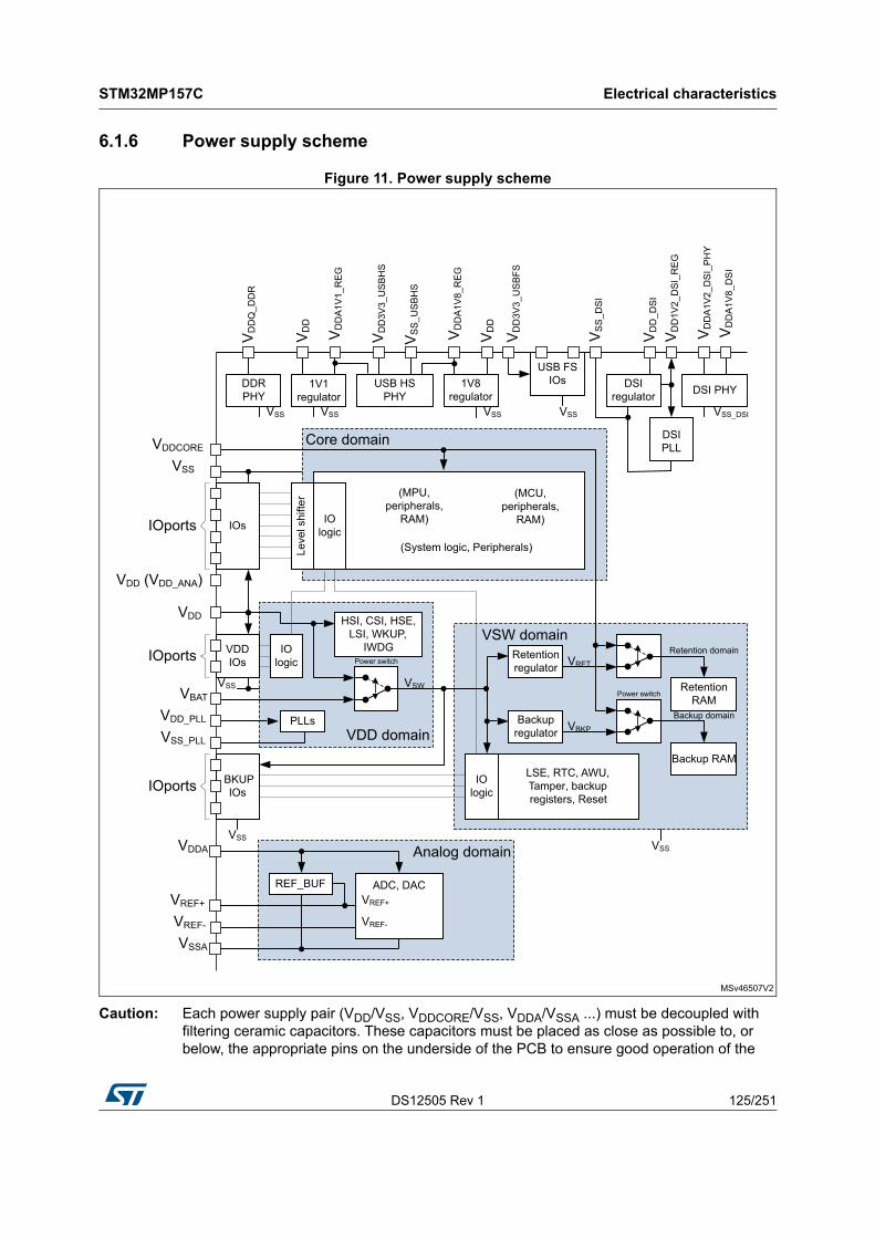
DS12505 Rev 1 125/251
STM32MP157C Electrical characteristics
234
6.1.6 Power supply scheme
Figure 11. Power supply scheme
Caution: Each power supply pair (VDD/VSS, VDDCORE/VSS, VDDA/VSSA ...) must be decoupled with filtering ceramic capacitors. These capacitors must be placed as close as possible to, or below, the appropriate pins on the underside of the PCB to ensure good operation of the
MSv46507V2
BKUP IOs
VDD domain
Analog domain
Core domain
VSW domain
(System logic, Peripherals)
(MPU, peripherals,
RAM)
Leve
l shi
fter
ADC, DAC
(MCU, peripherals,
RAM)
Power switch
VDDCORE
VSS
VBAT
VDDA
VREF+
VREF-
VSSA
Backupregulator
VDD
Backup RAM
Power switch
HSI, CSI, HSE, LSI, WKUP,
IWDG
IOs
DSIregulator
VD
D_D
SI
VD
D1V
2_D
SI_
RE
G
VS
S_D
SI
VSS
VSS
REF_BUF
VSS
IOlogic
VREF+
DSIPLL
VSW
LSE, RTC, AWU, Tamper, backup registers, Reset
IOlogic
VBKP
Retention RAM
Retentionregulator VRET
1V8regulator
VD
DA
1V8_
RE
G
VD
D
VSS
Backup domain
Retention domainVDDIOs
IOlogic
USB FS IOs
VSS
VD
D3V
3_U
SB
FS
USB HS PHY
VD
D3V
3_U
SB
HS
DSI PHY
VD
DA
1V2_
DS
I_P
HY
VD
DA
1V8_
DS
IVDD_PLL PLLs
DDRPHY
VD
DQ
_DD
R
VSS VSS_DSI
1V1regulator
VSS
VD
DA
1V1_
RE
G
VSS_PLL
VD
D
VS
S_U
SB
HS
VREF-
IOports
IOports
IOports
VDD (VDD_ANA)
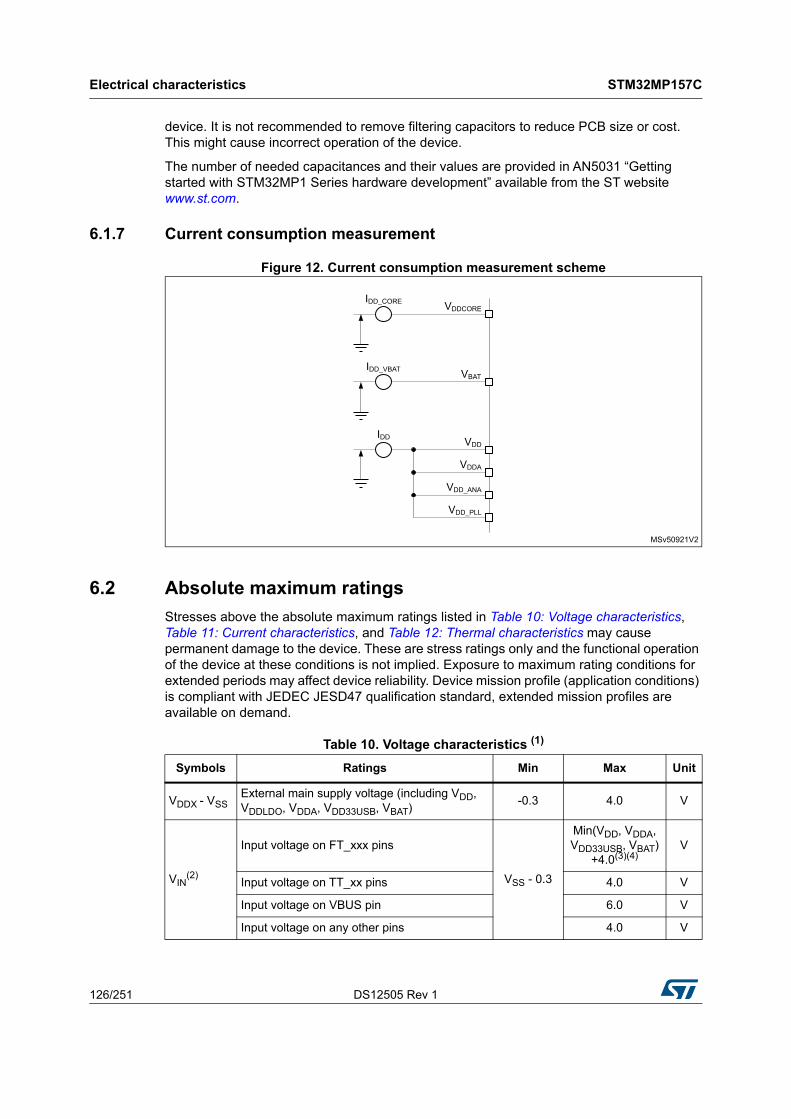
Electrical characteristics STM32MP157C
126/251 DS12505 Rev 1
device. It is not recommended to remove filtering capacitors to reduce PCB size or cost. This might cause incorrect operation of the device.
The number of needed capacitances and their values are provided in AN5031 “Getting started with STM32MP1 Series hardware development” available from the ST website www.st.com.
6.1.7 Current consumption measurement
Figure 12. Current consumption measurement scheme
6.2 Absolute maximum ratings
Stresses above the absolute maximum ratings listed in Table 10: Voltage characteristics, Table 11: Current characteristics, and Table 12: Thermal characteristics may cause permanent damage to the device. These are stress ratings only and the functional operation of the device at these conditions is not implied. Exposure to maximum rating conditions for extended periods may affect device reliability. Device mission profile (application conditions) is compliant with JEDEC JESD47 qualification standard, extended mission profiles are available on demand.
MSv50921V2
IDD_CORE VDDCORE
IDD_VBAT VBAT
IDD
VDDA
VDD
VDD_ANA
VDD_PLL
Table 10. Voltage characteristics (1)
Symbols Ratings Min Max Unit
VDDX - VSSExternal main supply voltage (including VDD, VDDLDO, VDDA, VDD33USB, VBAT)
-0.3 4.0 V
VIN(2)
Input voltage on FT_xxx pins
VSS - 0.3
Min(VDD, VDDA, VDD33USB, VBAT)
+4.0(3)(4)V
Input voltage on TT_xx pins 4.0 V
Input voltage on VBUS pin 6.0 V
Input voltage on any other pins 4.0 V

DS12505 Rev 1 127/251
STM32MP157C Electrical characteristics
234
|∆VDDX|Variations between different VDDX power pins of the same domain
- 50 mV
|VSSx-VSS| Variations between all the different ground pins - 50 mV
1. All main power (VDD, VDDA, VDD33USB, VBAT) and ground (VSS, VSSA) pins must always be connected to the external power supply, in the permitted range.
2. VIN maximum must always be respected. Refer to Table 49 for the maximum allowed injected current values.
3. This formula has to be applied on power supplies related to the IO structure described by the pin definition table.
4. To sustain a voltage higher than 4 V the internal pull-up/pull-down resistors must be disabled.
Table 11. Current characteristics
Symbols Ratings Max Unit
ΣIVDD Total current into sum of all VDD power lines (source)(1)
1. All main power (VDD, VDDA, VDD33USB) and ground (VSS, VSSA) pins must always be connected to the external power supplies, in the permitted range.
TBD
mA
ΣIVSS Total current out of sum of all VSS ground lines (sink)(1) TBD
IVDD Maximum current into each VDD power pin (source)(1) 100
IVSS Maximum current out of each VSS ground pin (sink)(1) 100
IIO Output current sunk by any I/O and control pin 20
ΣI(PIN)
Total output current sunk by sum of all I/Os and control pins(2)
2. This current consumption must be correctly distributed over all I/Os and control pins. The total output current must not be sunk/sourced between two consecutive power supply pins referring to high pin count QFP packages.
140
Total output current sourced by sum of all I/Os and control pins(2) 140
IINJ(PIN)(3)(4)
3. Positive injection is not possible on these I/Os and does not occur for input voltages lower than the specified maximum value.
4. A positive injection is induced by VIN>VDD while a negative injection is induced by VIN<VSS. IINJ(PIN) must never be exceeded. Refer also to Table 10: Voltage characteristics for the maximum allowed input voltage values.
Injected current on FT_xxx, TT_xx, RST and B pins except PA4, PA5
-5/+0
Injected current on PA4, PA5 -0/0
ΣIINJ(PIN) Total injected current (sum of all I/Os and control pins)(5)
5. When several inputs are submitted to a current injection, the maximum ∑IINJ(PIN) is the absolute sum of the positive and negative injected currents (instantaneous values).
±25
Table 12. Thermal characteristics
Symbol Ratings Value Unit
TSTG Storage temperature range -65 to +150°C
TJ Maximum junction temperature 125
Table 10. Voltage characteristics (continued)(1)
Symbols Ratings Min Max Unit
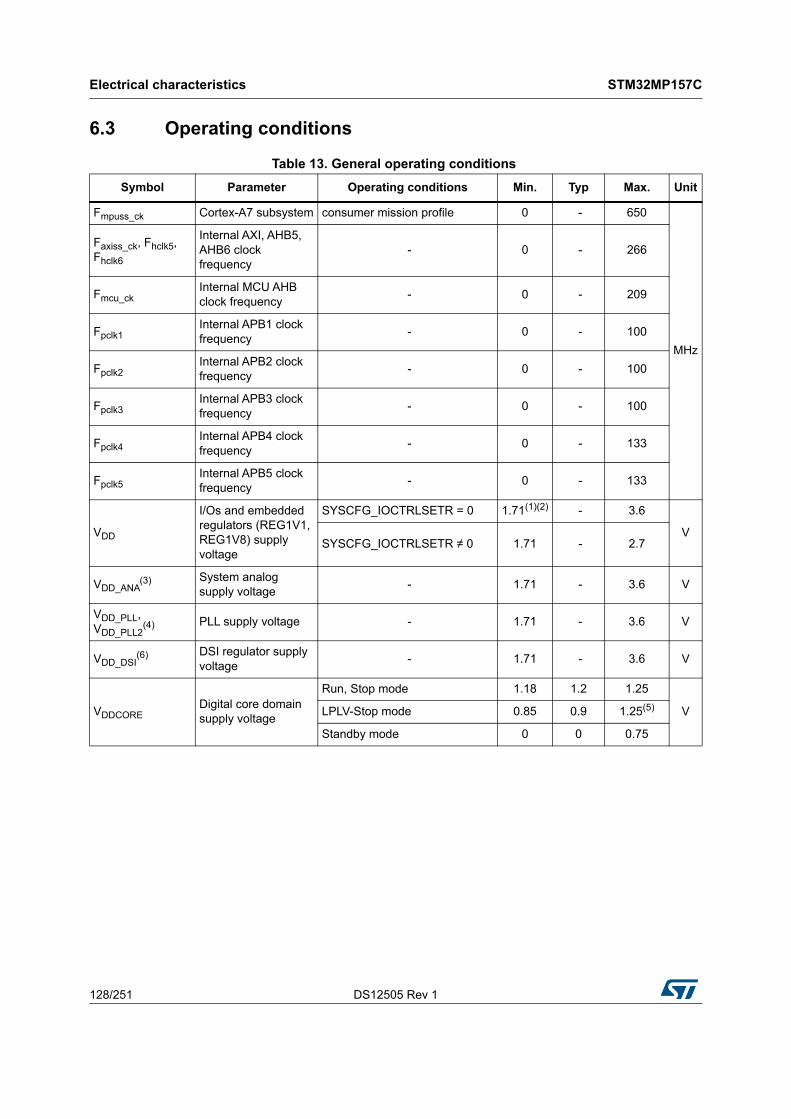
Electrical characteristics STM32MP157C
128/251 DS12505 Rev 1
6.3 Operating conditions
Table 13. General operating conditions
Symbol Parameter Operating conditions Min. Typ Max. Unit
Fmpuss_ck Cortex-A7 subsystem consumer mission profile 0 - 650
MHz
Faxiss_ck, Fhclk5, Fhclk6
Internal AXI, AHB5, AHB6 clock frequency
- 0 - 266
Fmcu_ckInternal MCU AHB clock frequency
- 0 - 209
Fpclk1Internal APB1 clock frequency
- 0 - 100
Fpclk2Internal APB2 clock frequency
- 0 - 100
Fpclk3Internal APB3 clock frequency
- 0 - 100
Fpclk4Internal APB4 clock frequency
- 0 - 133
Fpclk5Internal APB5 clock frequency
- 0 - 133
VDD
I/Os and embedded regulators (REG1V1, REG1V8) supply voltage
SYSCFG_IOCTRLSETR = 0 1.71(1)(2) - 3.6
VSYSCFG_IOCTRLSETR ≠ 0 1.71 - 2.7
VDD_ANA(3) System analog
supply voltage - 1.71 - 3.6 V
VDD_PLL, VDD_PLL2
(4) PLL supply voltage - 1.71 - 3.6 V
VDD_DSI(6) DSI regulator supply
voltage - 1.71 - 3.6 V
VDDCOREDigital core domain supply voltage
Run, Stop mode 1.18 1.2 1.25
VLPLV-Stop mode 0.85 0.9 1.25(5)
Standby mode 0 0 0.75
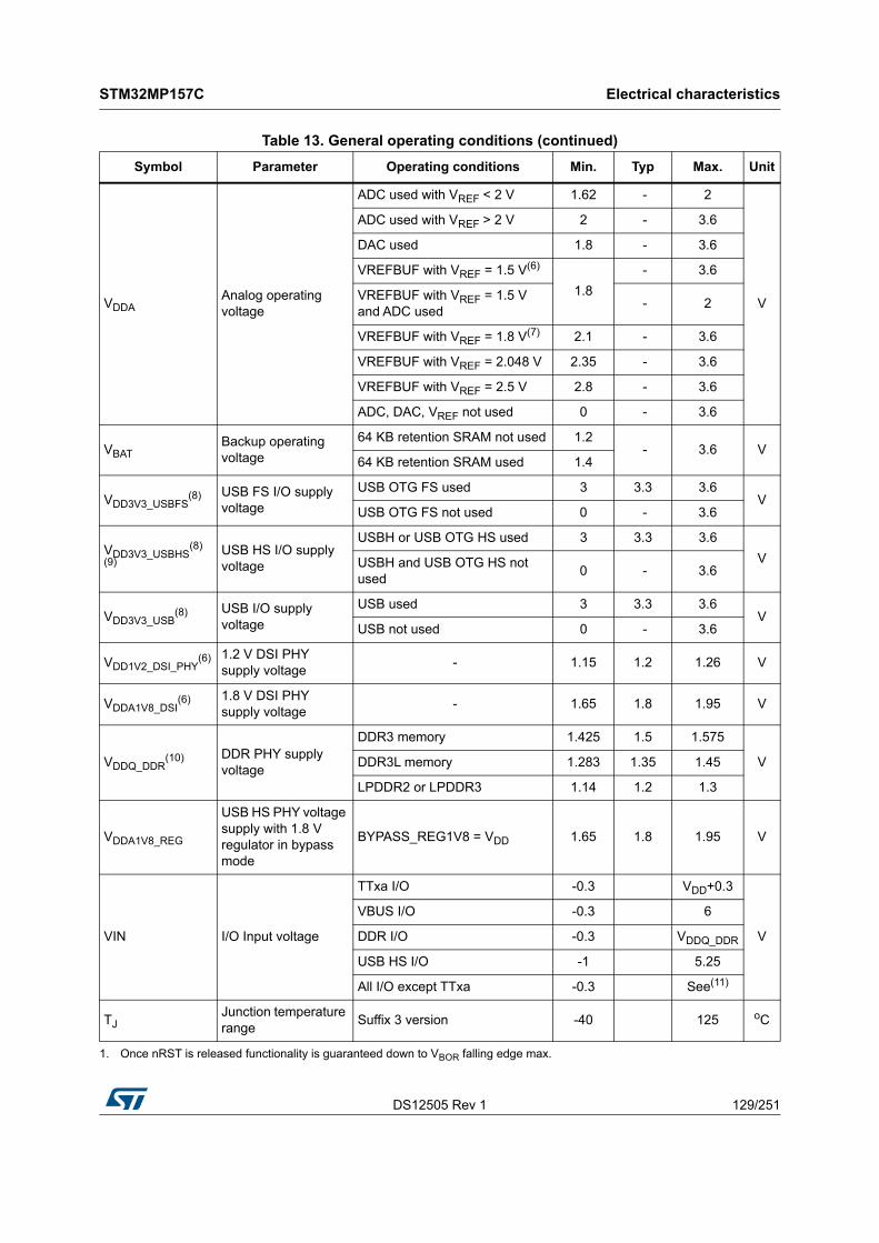
DS12505 Rev 1 129/251
STM32MP157C Electrical characteristics
234
VDDAAnalog operating voltage
ADC used with VREF < 2 V 1.62 - 2
V
ADC used with VREF > 2 V 2 - 3.6
DAC used 1.8 - 3.6
VREFBUF with VREF = 1.5 V(6)
1.8
- 3.6
VREFBUF with VREF = 1.5 V and ADC used
- 2
VREFBUF with VREF = 1.8 V(7) 2.1 - 3.6
VREFBUF with VREF = 2.048 V 2.35 - 3.6
VREFBUF with VREF = 2.5 V 2.8 - 3.6
ADC, DAC, VREF not used 0 - 3.6
VBATBackup operating voltage
64 KB retention SRAM not used 1.2 - 3.6 V
64 KB retention SRAM used 1.4
VDD3V3_USBFS(8) USB FS I/O supply
voltage
USB OTG FS used 3 3.3 3.6V
USB OTG FS not used 0 - 3.6
VDD3V3_USBHS(8)
(9)USB HS I/O supply voltage
USBH or USB OTG HS used 3 3.3 3.6
VUSBH and USB OTG HS not used
0 - 3.6
VDD3V3_USB(8) USB I/O supply
voltage
USB used 3 3.3 3.6V
USB not used 0 - 3.6
VDD1V2_DSI_PHY(6) 1.2 V DSI PHY
supply voltage - 1.15 1.2 1.26 V
VDDA1V8_DSI(6) 1.8 V DSI PHY
supply voltage - 1.65 1.8 1.95 V
VDDQ_DDR(10) DDR PHY supply
voltage
DDR3 memory 1.425 1.5 1.575
VDDR3L memory 1.283 1.35 1.45
LPDDR2 or LPDDR3 1.14 1.2 1.3
VDDA1V8_REG
USB HS PHY voltage supply with 1.8 V regulator in bypass mode
BYPASS_REG1V8 = VDD 1.65 1.8 1.95 V
VIN I/O Input voltage
TTxa I/O -0.3 VDD+0.3
V
VBUS I/O -0.3 6
DDR I/O -0.3 VDDQ_DDR
USB HS I/O -1 5.25
All I/O except TTxa -0.3 See(11)
TJJunction temperature range
Suffix 3 version -40 125 oC
1. Once nRST is released functionality is guaranteed down to VBOR falling edge max.
Table 13. General operating conditions (continued)
Symbol Parameter Operating conditions Min. Typ Max. Unit

Electrical characteristics STM32MP157C
130/251 DS12505 Rev 1
6.3.1 General operating conditions
6.3.2 Operating conditions at power-up / power-down
Subject to general operating conditions.
2. Min VDD is 2.25 V when REG1V8 is used BYPASS_REG1V8 = 0.
3. Should be connected to same power supply voltage as VDD.
4. It is recommended to connect VDD_PLL and VDD_PLL2 to same power supply as VDD.
5. 1.25 V is the max allowed voltage, however LPLV-Stop mode is only relevant for VDDCORE up to 0.95 V. In LPLV-Stop mode, if VDDQ_DDR is not shutdown, to avoid overconsumption on VDDQ_DDR, the DDR memory must be put in SelfRefresh and DDR PHY must be set in retention mode (setting bit DDRRETEN: DDR retention enable of PWR control register 3 (PWR_CR3)).
6. DAC cannot be used with VREF below 1.8 V.
7. ADC cannot be used with VREF below 2 V and VDDA above 2 V.
8. Depending on package selected, either VDD3V3_USBFS and VDD3V3_USBHS or only VDD3V3_USB are available.
9. For operation with voltage higher than Min (VDD, VDDA, VDD3V3_USBFS) +0.3 V, the internal Pull-up and Pull-Down resistors must be disabled.
10. Independent from any other supply.
11. Min(VDD, VDDA, VDD3V3_USBFS) +3.6 V < 5.5 V. This formula has to be applied on power supplies related to the IO structure described by the pin definition table.
Table 14. Operating conditions at power-up / power-down
Symbol Parameter Min Max Unit
tVDD(1)
1. VDD must be present before VDDCORE .
VDD rise time rate 0 ∞
µs/V
VDD fall time rate 10 ∞
tVDDA
VDDA rise time rate 0 ∞
VDDA fall time rate 10 ∞
tVDD3V3_USB(2)
tVDD3V3_USBHS
tVDD3V3_USBFS
2. VDDA1V8_REG must be present before VDD3V3_USBHS.
VDD3V3_USBxx rise time rate 0 ∞
VDD3V3_USBxx fall time rate 10 ∞
tVDDCORE
VDDCORE rise time rate (from reset to RUN mode)
2000(3)
3. In case VDDCORE rise time is larger than 2 ms/V, user should control the NRST_CORE signal with a Power Good (PG) control signal from the external regulator to avoid dysfunction of the device due to VDDCORE potentially not yet established when internal reset signal is de-activated after tVDDCORETEMPO (cf.Table 14 and Figure 13).
VDDCORE rise time rate (from LPLV-Stop to RUN mode)
1000(4)
4. In case VDDCORE rise time at exit of LPLV-Stop is larger than 1 ms/V, there is a risk of unwanted reset due to VDDCORE potentially not yet established after tSEL_VDDCORETEMPO (cf.Table 14 and Figure 14). In such a case, the VDDCORE supply should not be decreased during LPLV-Stop mode.
VDDCORE fall time rate 7.33 ∞
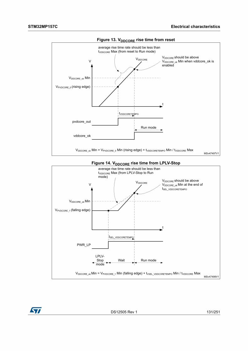
DS12505 Rev 1 131/251
STM32MP157C Electrical characteristics
234
Figure 13. VDDCORE rise time from reset
Figure 14. VDDCORE rise time from LPLV-Stop
MSv47497V1
VDDCORE
t
pvdcore_out
tVDDCORETEMPO
VDDCORE should be aboveVDDCORE_ok Min when vddcore_ok is enabled
VPVDCORE_0 (rising edge)
vddcore_ok
Run mode
VDDCORE_ok Min = VPVDCORE_0 Min (rising edge) + tVDDCORETEMPO Min / tVDDCORE Max
average rise time rate should be less than tVDDCORE Max (from reset to Run mode)
V
VDDCORE_ok Min
MSv47499V1
VDDCORE
t
PWR_LP
tSEL_VDDCORETEMPO
VDDCORE should be aboveVDDCORE_ok Min at the end of tSEL_VDDCORETEMPO
VPVDCORE_1 (falling edge)
Run mode
VDDCORE_ok Min = VPVDCORE_1 Min (falling edge) + tVSEL_VDDCORETEMPO Min / tVDDCORE Max
average rise time rate should be less than tVDDCORE Max (from LPLV-Stop to Run mode)
V
VDDCORE_ok Min
WaitLPLV-Stop mode

Electrical characteristics STM32MP157C
132/251 DS12505 Rev 1
6.3.3 Embedded reset and power control block characteristics
The parameters given in Table 15 are derived from tests performed under ambient
temperature and VDD supply voltage conditions summarized in Table 13: General operating conditions.
Table 15. Embedded reset and power control block characteristics
Symbol Parameter Conditions Min Typ Max Unit
tRSTTEMPO(1) Reset temporization. after
BOR0 released - - 377 550 µs
VBOR0(1) Brown-out reset threshold 0
Rising edge 1.62 1.67 1.71V
Falling edge 1.58 1.63 1.67
VBOR1 Brown-out reset threshold 1Rising edge 2.055 2.1 2.145
VFalling edge 1.955 2 2.045
VBOR2 Brown-out reset threshold 2Rising edge 2.355 2.4 2.445
VFalling edge 2.255 2.3 2.345
VBOR3 Brown-out reset threshold 3Rising edge 2.655 2.7 2.745
VFalling edge 2.555 2.6 2.645
VPVD0Programmable Voltage Detector threshold 0
Rising edge 1.905 1.95 1.995V
Falling edge 1.805 1.85 1.895
VPVD1Programmable Voltage Detector threshold 1
Rising edge 2.055 2.1 2.145V
Falling edge 1.955 2 2.045
VPVD2Programmable Voltage Detector threshold 2
Rising edge 2.205 2.25 2.295V
Falling edge 2.105 2.15 2.195
VPVD3Programmable Voltage Detector threshold 3
Rising edge 2.355 2.4 2.445V
Falling edge 2.255 2.3 2.345
VPVD4Programmable Voltage Detector threshold 4
Rising edge 2.505 2.55 2.595V
Falling edge 2.405 2.45 2.495
VPVD5Programmable Voltage Detector threshold 5
Rising edge 2.655 2.7 2.745V
Falling edge 2.555 2.6 2.645
VPVD6Programmable Voltage Detector threshold 6
Rising edge 2.805 2.85 2.895
VFalling edge in RUN mode
2.705 2.75 2.795
Vhyst_BOR0 Hysteresis voltage of BOR0Hysteresis in RUN mode
- 40 - mV
Vhyst_BOR Hysteresis voltage of BOR Unless BOR0 - 100 - mV
Vhyst_BOR_PVDHysteresis voltage of BOR (unless BOR0) and PVD(2)
Hysteresis in RUN mode
- 100 - mV
IDD_BOR_PVD(1)(3) BOR (unless BOR0) and PVD
consumption from VDD0.246 - 0.626 µA
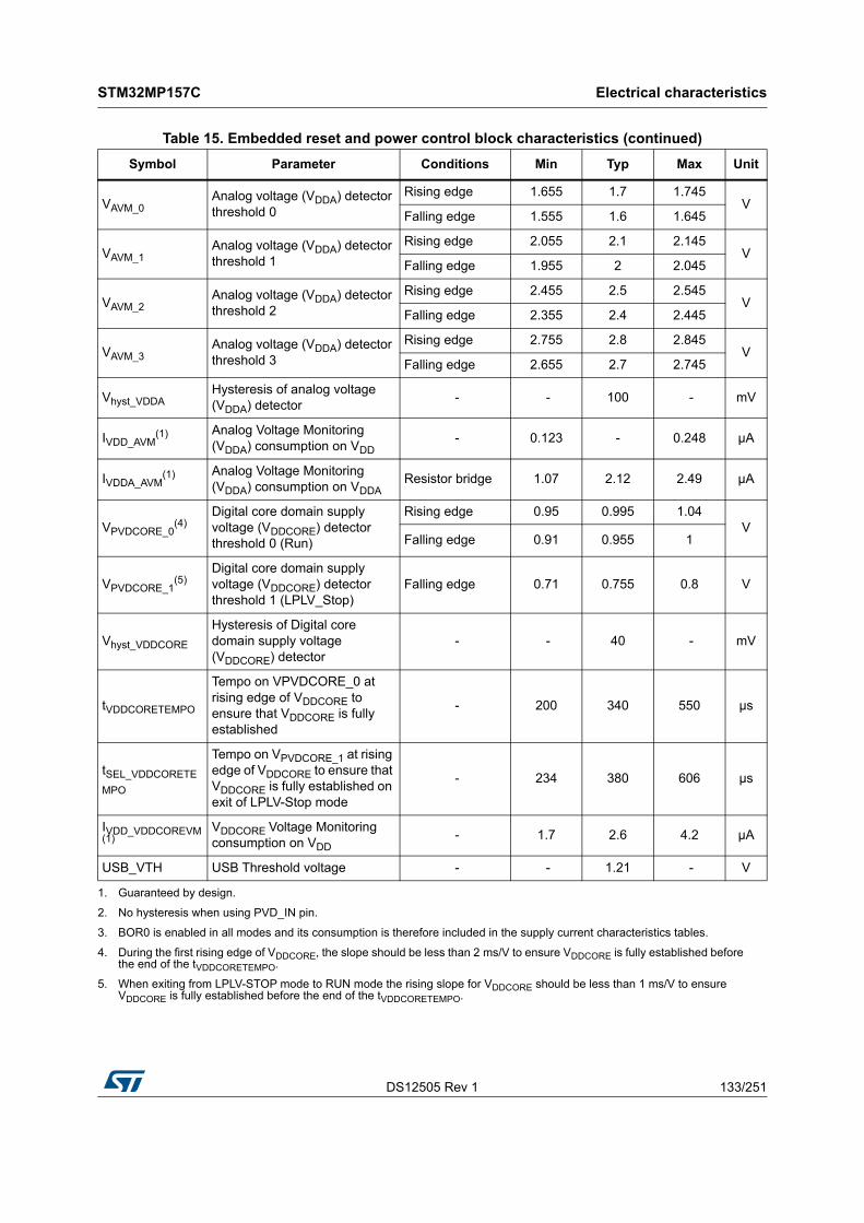
DS12505 Rev 1 133/251
STM32MP157C Electrical characteristics
234
VAVM_0Analog voltage (VDDA) detector threshold 0
Rising edge 1.655 1.7 1.745V
Falling edge 1.555 1.6 1.645
VAVM_1Analog voltage (VDDA) detector threshold 1
Rising edge 2.055 2.1 2.145V
Falling edge 1.955 2 2.045
VAVM_2Analog voltage (VDDA) detector threshold 2
Rising edge 2.455 2.5 2.545V
Falling edge 2.355 2.4 2.445
VAVM_3Analog voltage (VDDA) detector threshold 3
Rising edge 2.755 2.8 2.845V
Falling edge 2.655 2.7 2.745
Vhyst_VDDAHysteresis of analog voltage (VDDA) detector
- - 100 - mV
IVDD_AVM(1) Analog Voltage Monitoring
(VDDA) consumption on VDD - 0.123 - 0.248 µA
IVDDA_AVM(1) Analog Voltage Monitoring
(VDDA) consumption on VDDAResistor bridge 1.07 2.12 2.49 µA
VPVDCORE_0(4)
Digital core domain supply voltage (VDDCORE) detector threshold 0 (Run)
Rising edge 0.95 0.995 1.04V
Falling edge 0.91 0.955 1
VPVDCORE_1(5)
Digital core domain supply voltage (VDDCORE) detector threshold 1 (LPLV_Stop)
Falling edge 0.71 0.755 0.8 V
Vhyst_VDDCORE
Hysteresis of Digital core domain supply voltage (VDDCORE) detector
- - 40 - mV
tVDDCORETEMPO
Tempo on VPVDCORE_0 at rising edge of VDDCORE to ensure that VDDCORE is fully established
- 200 340 550 µs
tSEL_VDDCORETE
MPO
Tempo on VPVDCORE_1 at rising edge of VDDCORE to ensure that VDDCORE is fully established on exit of LPLV-Stop mode
- 234 380 606 µs
IVDD_VDDCOREVM(1)
VDDCORE Voltage Monitoring consumption on VDD
- 1.7 2.6 4.2 µA
USB_VTH USB Threshold voltage - - 1.21 - V
1. Guaranteed by design.
2. No hysteresis when using PVD_IN pin.
3. BOR0 is enabled in all modes and its consumption is therefore included in the supply current characteristics tables.
4. During the first rising edge of VDDCORE, the slope should be less than 2 ms/V to ensure VDDCORE is fully established before the end of the tVDDCORETEMPO.
5. When exiting from LPLV-STOP mode to RUN mode the rising slope for VDDCORE should be less than 1 ms/V to ensure VDDCORE is fully established before the end of the tVDDCORETEMPO.
Table 15. Embedded reset and power control block characteristics (continued)
Symbol Parameter Conditions Min Typ Max Unit
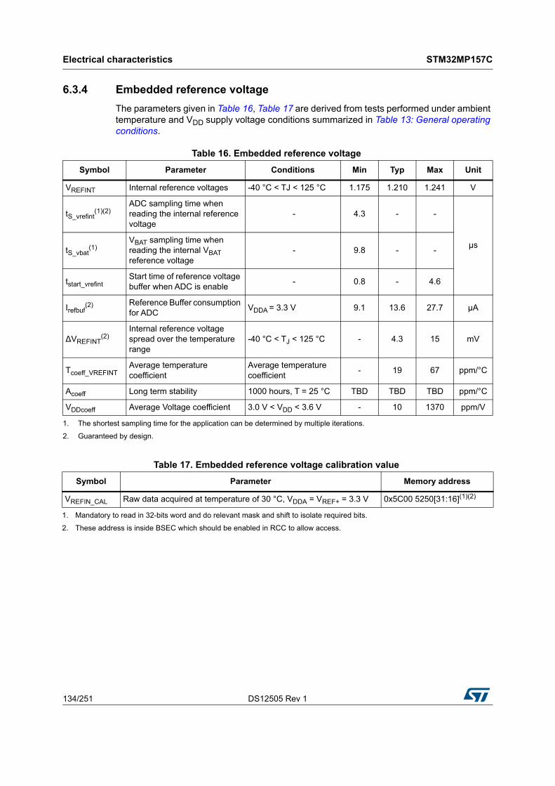
Electrical characteristics STM32MP157C
134/251 DS12505 Rev 1
6.3.4 Embedded reference voltage
The parameters given in Table 16, Table 17 are derived from tests performed under ambient temperature and VDD supply voltage conditions summarized in Table 13: General operating conditions.
Table 16. Embedded reference voltage
Symbol Parameter Conditions Min Typ Max Unit
VREFINT Internal reference voltages -40 °C < TJ < 125 °C 1.175 1.210 1.241 V
tS_vrefint(1)(2)
ADC sampling time when reading the internal reference voltage
- 4.3 - -
µstS_vbat
(1)VBAT sampling time when reading the internal VBAT reference voltage
- 9.8 - -
tstart_vrefintStart time of reference voltage buffer when ADC is enable
- 0.8 - 4.6
Irefbuf(2) Reference Buffer consumption
for ADCVDDA = 3.3 V 9.1 13.6 27.7 µA
∆VREFINT(2)
Internal reference voltage spread over the temperature range
-40 °C < TJ < 125 °C - 4.3 15 mV
Tcoeff_VREFINTAverage temperature coefficient
Average temperature coefficient
- 19 67 ppm/°C
Acoeff Long term stability 1000 hours, T = 25 °C TBD TBD TBD ppm/°C
VDDcoeff Average Voltage coefficient 3.0 V < VDD < 3.6 V - 10 1370 ppm/V
1. The shortest sampling time for the application can be determined by multiple iterations.
2. Guaranteed by design.
Table 17. Embedded reference voltage calibration value
Symbol Parameter Memory address
VREFIN_CAL Raw data acquired at temperature of 30 °C, VDDA = VREF+ = 3.3 V 0x5C00 5250[31:16](1)(2)
1. Mandatory to read in 32-bits word and do relevant mask and shift to isolate required bits.
2. These address is inside BSEC which should be enabled in RCC to allow access.
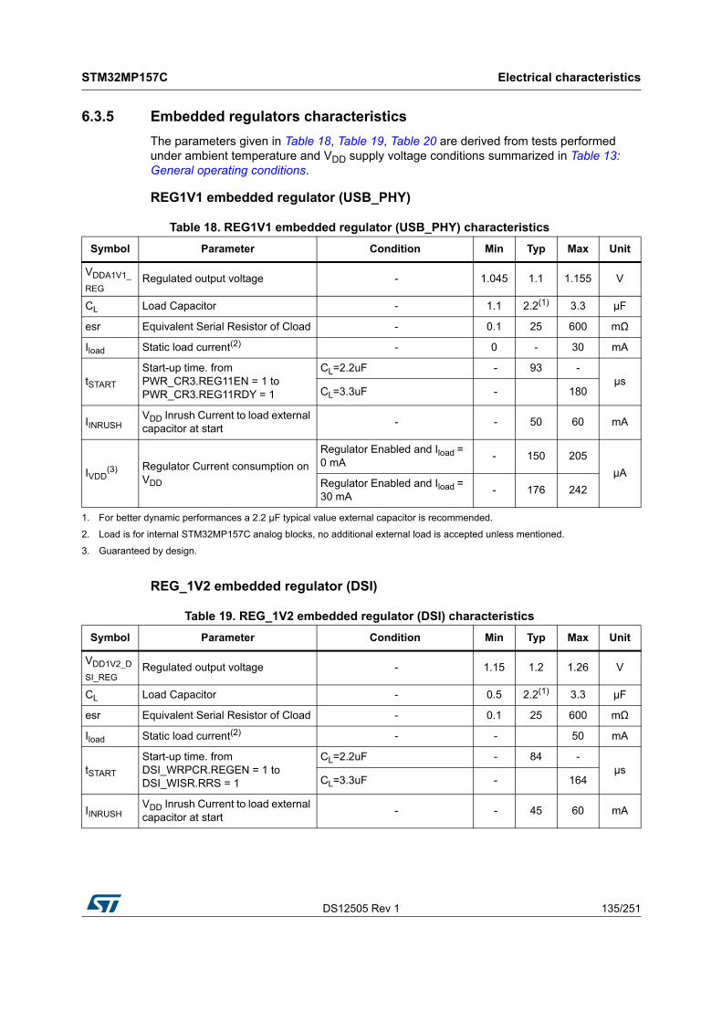
DS12505 Rev 1 135/251
STM32MP157C Electrical characteristics
234
6.3.5 Embedded regulators characteristics
The parameters given in Table 18, Table 19, Table 20 are derived from tests performed under ambient temperature and VDD supply voltage conditions summarized in Table 13: General operating conditions.
REG1V1 embedded regulator (USB_PHY)
REG_1V2 embedded regulator (DSI)
Table 18. REG1V1 embedded regulator (USB_PHY) characteristics
Symbol Parameter Condition Min Typ Max Unit
VDDA1V1_
REGRegulated output voltage - 1.045 1.1 1.155 V
CL Load Capacitor - 1.1 2.2(1) 3.3 µF
esr Equivalent Serial Resistor of Cload - 0.1 25 600 mΩ
Iload Static load current(2) - 0 - 30 mA
tSTART
Start-up time. from PWR_CR3.REG11EN = 1 to PWR_CR3.REG11RDY = 1
CL=2.2uF - 93 -µs
CL=3.3uF - 180
IINRUSHVDD Inrush Current to load external capacitor at start
- - 50 60 mA
IVDD(3) Regulator Current consumption on
VDD
Regulator Enabled and Iload = 0 mA
- 150 205
µARegulator Enabled and Iload = 30 mA
- 176 242
1. For better dynamic performances a 2.2 μF typical value external capacitor is recommended.
2. Load is for internal STM32MP157C analog blocks, no additional external load is accepted unless mentioned.
3. Guaranteed by design.
Table 19. REG_1V2 embedded regulator (DSI) characteristics
Symbol Parameter Condition Min Typ Max Unit
VDD1V2_D
SI_REGRegulated output voltage - 1.15 1.2 1.26 V
CL Load Capacitor - 0.5 2.2(1) 3.3 µF
esr Equivalent Serial Resistor of Cload - 0.1 25 600 mΩ
Iload Static load current(2) - - 50 mA
tSTART
Start-up time. from DSI_WRPCR.REGEN = 1 to DSI_WISR.RRS = 1
CL=2.2uF - 84 -µs
CL=3.3uF - 164
IINRUSHVDD Inrush Current to load external capacitor at start
- - 45 60 mA

Electrical characteristics STM32MP157C
136/251 DS12505 Rev 1
REG_1V8 embedded regulator (USB+DSI)
6.3.6 Supply current characteristics
The current consumption is a function of several parameters and factors such as the operating voltage, ambient temperature, I/O pin loading, device software configuration, operating frequencies, I/O pin switching rate, program location in memory and executed binary code.
The current consumption is measured as described in Figure 12: Current consumption measurement scheme.
All the Run mode current consumption measurements given in this section are performed with a CoreMark code unless otherwise specified.
IVDDRegulator Current consumption on VDD
Regulator Enabled and Iload = 0 mA
- 150 203(3)
µARegulator Enabled and Iload = 50 mA
- 178(3) 243(3)
1. For better dynamic performances a 2.2 μF typical value external capacitor is recommended.
2. Load is for internal STM32MP157C analog blocks, no additional external load is accepted unless mentioned.
3. Guaranteed by design.
Table 19. REG_1V2 embedded regulator (DSI) characteristics (continued)
Symbol Parameter Condition Min Typ Max Unit
Table 20. REG_1V8 embedded regulator (USB+DSI) characteristics
Symbol Parameter Condition Min Typ Max Unit
VDD Regulator input voltage - 2.25 3.3 3.6 V
VDDA1V8_
REGRegulated output voltage after trimming 1.7 1.8 1.9 V
CL Load Capacitor - 0.5 2.2(1) 3.3 µF
esr Equivalent Serial Resistor of Cload - 0.1 25 600 mΩ
Iload Static load current(2) - - - 70 mA
tSTART
Start-up time. from PWR_CR3.REG11EN = 1 to PWR_CR3.REG11RDY = 1
CL=2.2uF - 81µs
CL=3.3uF - 150
IINRUSHVDD Inrush Current to load external capacitor at start
- - 80 100 mA
IVDD(3) Regulator Current consumption on
VDD
Regulator Enabled and Iload = 0 mA
- 130 181
µARegulator Enabled and Iload = 70 mA
- 170 231
1. For better dynamic performances a 2.2 μF typical value external capacitor is recommended.
2. Load is for internal STM32MP157C analog blocks, no additional external load is accepted unless mentioned.
3. Guaranteed by design.

DS12505 Rev 1 137/251
STM32MP157C Electrical characteristics
234
Typical and maximum current consumption
The device is placed under the following conditions:
• All I/O pins are in analog input mode except when explicitly mentioned.
• All peripherals are disabled except when explicitly mentioned.
• The maximum values are obtained for VDD/VBAT = 3.6 V and VDDCORE = 1.25 V, and the typical values for VDD/VBAT = 3.3 V and VDDCORE = 1.2 V unless otherwise specified.
The parameters given in Table 22 to Table 26 are derived from tests performed under supply voltage conditions summarized in Table 13: General operating conditions.

Elec
trical c
hara
cteristic
sS
TM
32
MP
157C
138/251
DS
1250
5 Rev 1
Table 21. Current consumption (IDDCORE) in Run mode(1)
Symbol Parameter
Conditions Typ Max
Unit-
MPU SS mode
MCU SS
modeOscillator
MPU clk
(MHz)
MCU clk
(MHz)
Tj = 25 °C
Tj = 25 °C
Tj = 55 °C
Tj = 85 °C
Tj = 105 °C
Tj = 125 °C
IDDCORE
Supply current in Run mode
All peripherals enabled
CRun (P0Run, P1Run)
CRun HSE+HSI+LSI+PLL
648
209
390 TBD TBD TBD TBD TBD
mA600 385 TBD TBD TBD TBD TBD
400 335 TBD TBD TBD TBD TBD
IDDCORE
Supply current in Run mode
All peripherals enabled
CRun (P0Run, P1Run)
CStop HSE+HSI+LSI+PLL
648
209
385 TBD TBD TBD TBD TBD
mA600 375 TBD TBD TBD TBD TBD
400 325 TBD TBD TBD TBD TBD
IDDCORE
Supply current in Run mode
All peripherals disabled
CRun (P0Run, P1Stop)
CStop
HSE+HSI+PLL 648 - 180 TBD TBD TBD TBD TBD
mA
HSE+HSI+PLL 600 - 175 TBD TBD TBD TBD TBD
HSE+HSI+PLL 300 - 135 TBD TBD TBD TBD TBD
HSE+HSI+PLL 150 - 92.0 TBD TBD TBD TBD TBD
HSE+HSI+PLL 64 - 65.5 TBD TBD TBD TBD TBD
HSE+HSI+PLL 24 - 51.5 TBD TBD TBD TBD TBD
HSE+HSI 24 - 35.5 TBD TBD TBD TBD TBD
HSI+PLL 64 - 65.0 - - - - -
HSI+PLL 24 - 51.5 - - - - -
HSI 64 - 49.0 - - - - -

ST
M3
2MP
157
CE
lectric
al cha
racte
ristic
s
DS
1250
5 Rev 1
139/251
IDDCORE
Supply current in Run mode
MPU in CSleep with WFI (CLK OFF). All peripherals disabled
CSleep (P0Stop, P1Stop)
CStop
HSE+HSI+PLL 648 - 110 TBD TBD TBD TBD TBD
mA
HSE+HSI+PLL 600 - 110 TBD TBD TBD TBD TBD
HSE+HSI+PLL 300 - 100 TBD TBD TBD TBD TBD
HSE+HSI+PLL 150 - 73.5 TBD TBD TBD TBD TBD
HSE+HSI+PLL 64 - 57.0 TBD TBD TBD TBD TBD
HSE+HSI+PLL 24 - 48.5 TBD TBD TBD TBD TBD
HSE+HSI 24 - 32.5 TBD TBD TBD TBD TBD
HSI+PLL 64 - 57.5 - - - - -
HSI+PLL 24 - 48.5 - - - - -
HSI 64 - 41.5 - - - - -
Table 21. Current consumption (IDDCORE) in Run mode(1) (continued)
Symbol Parameter
Conditions Typ Max
Unit-
MPU SS mode
MCU SS
modeOscillator
MPU clk
(MHz)
MCU clk
(MHz)
Tj = 25 °C
Tj = 25 °C
Tj = 55 °C
Tj = 85 °C
Tj = 105 °C
Tj = 125 °C

Elec
trical c
hara
cteristic
sS
TM
32
MP
157C
140/251
DS
1250
5 Rev 1
IDDCORE
Supply current in Run mode
All peripherals disabled
CStop (P0Stop, P1Stop)
CRun
HSE+HSI+PLL - 209 71.0 TBD TBD TBD TBD TBD
mA
HSE+HSI+PLL - 100 52.5 TBD TBD TBD TBD TBD
HSE+HSI+PLL - 64 59.5 TBD TBD TBD TBD TBD
HSE+HSI+PLL - 24 53.0 TBD TBD TBD TBD TBD
HSE+HSI+PLL - 10 38.5 TBD TBD TBD TBD TBD
HSE+HSI+PLL - 4 37.5 TBD TBD TBD TBD TBD
HSE+HSI - 24 27.0 TBD TBD TBD TBD TBD
HSI+PLL - 64 59.5 - - - - -
HSI+PLL - 24 53.0 - - - - -
HSI - 64 33.0 - - - - -
CSI+HSI+PLL - 64 59.5 - - - - -
CSI+HSI+PLL - 24 53.0 - - - - -
CSI+HSI+PLL - 4 37.5 - - - - -
CSI+HSI - 4 23.5 - - - - -
Table 21. Current consumption (IDDCORE) in Run mode(1) (continued)
Symbol Parameter
Conditions Typ Max
Unit-
MPU SS mode
MCU SS
modeOscillator
MPU clk
(MHz)
MCU clk
(MHz)
Tj = 25 °C
Tj = 25 °C
Tj = 55 °C
Tj = 85 °C
Tj = 105 °C
Tj = 125 °C

ST
M3
2MP
157
CE
lectric
al cha
racte
ristic
s
DS
1250
5 Rev 1
141/251
IDDCORE
Supply current in Run mode
MCU in CSleep with WFI (CLK OFF). All peripherals disabled
CStop (P0Stop, P1Stop)
CSleep
HSE+HSI+PLL - 209 60.0 TBD TBD TBD TBD TBD
mA
HSE+HSI+PLL - 100 47.5 TBD TBD TBD TBD TBD
HSE+HSI+PLL - 64 56.0 TBD TBD TBD TBD TBD
HSE+HSI+PLL - 24 52.0 TBD TBD TBD TBD TBD
HSE+HSI+PLL - 10 38.0 TBD TBD TBD TBD TBD
HSE+HSI+PLL - 4 37.5 TBD TBD TBD TBD TBD
HSE+HSI - 24 25.5 TBD TBD TBD TBD TBD
HSI+PLL - 64 56.0 - - - - -
HSI+PLL - 24 51.5 - - - - -
HSI - 64 30.5 - - - - -
CSI+HSI+PLL - 64 56.0 - - - - -
CSI+HSI+PLL - 24 51.5 - - - - -
CSI+HSI+PLL - 4 37.0 - - - - -
CSI+HSI - 4 23.5 - - - - -
1. HSE = 24 MHz, AXI clk (Faxiss_ck) = Max(Fmpuss_ck, 264).
Table 21. Current consumption (IDDCORE) in Run mode(1) (continued)
Symbol Parameter
Conditions Typ Max
Unit-
MPU SS mode
MCU SS
modeOscillator
MPU clk
(MHz)
MCU clk
(MHz)
Tj = 25 °C
Tj = 25 °C
Tj = 55 °C
Tj = 85 °C
Tj = 105 °C
Tj = 125 °C

Elec
trical c
hara
cteristic
sS
TM
32
MP
157C
142/251
DS
1250
5 Rev 1
Table 22. Current consumption (IDD) in Run mode(1)
Symbol Parameter
Conditions Typ Max
UnitMPU SS mode
MCU SS
modeOscillator
Tj = 25 °C
Tj = 25 °C
Tj = 55 °C
Tj = 85 °C
Tj = 105 °C
Tj = 125 °C
IDD Supply current in Run modeCRun (P0Run, P1Run)
CRun HSE+HSI+LSI+PLL1,2,3,4 3.95 TBD TBD TBD TBD TBD mA
IDD Supply current in Run modeCRun (P0Run, P1Stop)
CStop
HSI+PLL1,2 3.00 TBD TBD TBD TBD TBD
mAHSE+HSI 1.75 TBD TBD TBD TBD TBD
HSI 1.25 TBD TBD TBD TBD TBD
1. HSE = 24 MHz.
Table 23. Current consumption in Stop mode(1)
Symbol Parameter
Conditions Typ Max
Unit-
MPU SS mode
MCU SS
mode
Tj =25 °C
Tj =55 °C
Tj =85 °C
Tj =105 °C
Tj =125 °C
Tj =25 °C
Tj =55 °C
Tj =85 °C
Tj =105 °C
Tj =125 °C
IDD
Supply current in Stop mode
All peripherals disabled
CStop (P0Stop, P1Stop)
CStop 980 980 985 985 995 TBD TBD TBD TBD TBD
µA
All peripherals disabled
CStandby (P0Stop, P1Stop)
CStop 980 980 985 985 995 TBD TBD TBD TBD TBD
IDDCORE
All peripherals disabled
CStop (P0Stop, P1Stop)
CStop 19000 42000 89500 150000 230000 TBD TBD TBD TBD TBD
All peripherals disabled
CStandby (P0Stop, P1Stop)
CStop 18500 42000 89000 150000 225000 TBD TBD TBD TBD TBD
1. HSE = 24 MHz.
ST
M3
2MP
157
CE
lectric
al cha
racte
ristic
s
DS
1250
5 Rev 1
143/251
Table 24. Current consumption in LPLV-Stop mode(1)
Symbol Parameter
Conditions Typ(2) Max(3)
Unit-
MPU SS mode
MCU SS
mode
Tj =25 °C
Tj =55 °C
Tj =85 °C
Tj =105 °C
Tj =125 °C
Tj =25 °C
Tj =55 °C
Tj =85 °C
Tj =105 °C
Tj =125 °C
IDD
Supply current in LPLV-Stop mode
All Peripheral disabled
CStop (P0Stop, P1Stop)
CStop 980 980 985 985 995 TBD TBD TBD TBD TBD
µA
All Peripheral disabled
CStandby (P0Stop, P1Stop)
CStop 980 980 985 985 995 TBD TBD TBD TBD TBD
IDDCORE
All Peripheral disabled
CStop (P0Stop, P1Stop)
CStop 6950 17000 39000 67500 105000 TBD TBD TBD TBD TBD
All Peripheral disabled
CStandby (P0Stop, P1Stop)
CStop 6950 17000 39000 67500 110000 TBD TBD TBD TBD TBD
1. HSE = 24 MHz.
2. VDDCORE = 0.9 V.
3. VDDCORE = 0.95 V.

Elec
trical c
hara
cteristic
sS
TM
32
MP
157C
144/251
DS
1250
5 Rev 1
Table 25. Current consumption in Standby mode(1)
Symbol Parameter
Conditions Typ Max
Unit-
MPU SS mode
MCU SS
mode
Tj =25 °C
Tj =55 °C
Tj =85 °C
Tj =105 °C
Tj =125 °C
Tj =25 °C
Tj =55 °C
Tj =85 °C
Tj =105 °C
Tj=125 °C
IDD
Supply current in Standby mode
Backup SRAM OFF, RTC OFF, LSE OFF
Retention RAM OFF
CStandby (P0Stop, P1Stop)
CStop 2.10 2.25 4.00 7.60 16.5 - - - - -
µABackup SRAM ON, RTC ON, LSE ON, medium_high drive
CStandby (P0Stop, P1Stop)
CStop 11.0 16.5 38.5 64.5 105 - - - - -
Retention RAM ON
CStandby (P0Stop, P1Stop)
CStop 96.0 175 460 800 1300 - - - - -
1. IWDG OFF, LSI OFF, VDDCORE = 0 V.
ST
M3
2MP
157
CE
lectric
al cha
racte
ristic
s
DS
1250
5 Rev 1
145/251
Table 26. Current consumption in VBAT mode
Symbol Parameter
Conditions Typ Max
Unit-
VBAT (V)
Tj =25 °C
Tj =55 °C
Tj =85 °C
Tj =105 °C
Tj =125 °C
Tj =25 °C
Tj =55 °C
Tj =85 °C
Tj =105 °C
Tj =125 °C
IDDVBAT
Supply current in VBAT mode
Backup SRAM OFF, RTC OFF, LSE OFF
Retention RAM OFF
1.6 0.007 0.022 0.130 0.395 1.10 - - - - -
µA
2.4 0.008 0.024 0.140 0.420 1.15 - - - - -
3 0.012 0.032 0.170 0.490 1.30 - - - - -
3.3 0.041 0.100 0.520 1.45 3.90 - - - - -
3.6 0.073 0.150 0.620 1.65 4.20 - - - - -
Backup SRAM OFF, RTC ON,. LSE ON, medium_high drive
1.6 7.80 14.0 32.5 54.5 88.5 - - - - -
2.4 8.35 14.5 33.5 55.5 89.0 - - - - -
3 8.75 15.0 34.5 57.5 92.0 - - - - -
3.3 9.15 15.5 35.5 59.5 96.0 - - - - -
3.6 9.95 16.0 36.5 61.0 98.0 - - - - -
Backup SRAM ON, RTC ON,. LSE ON, high drive
1.6 7.90 14.5 32.0 55.5 90.0 - - - - -
2.4 8.50 15.0 33.0 57.0 91.0 - - - - -
3 9.15 16.0 34.5 58.5 93.5 - - - - -
3.3 8.85 16.5 35.5 61.0 98.0 - - - - -
3.6 10.0 17.0 36.5 62.5 100 - - - - -

Elec
trical c
hara
cteristic
sS
TM
32
MP
157C
146/251
DS
1250
5 Rev 1
IDDVBAT
Supply current in VBAT mode
Backup SRAM ON, RTC ON,. LSE ON, medium_high drive
Retention RAM ON
1.6 74.0 165 415 770 1250 - - - - -
µA
2.4 76.5 170 415 775 1250 - - - - -
3 86.5 175 425 795 1300 - - - - -
3.3 79.0 175 430 805 1300 - - - - -
3.6 84.0 175 440 820 1350 - - - - -
Backup SRAM ON, RTC ON, LSE ON, high drive
1.6 74.0 165 415 780 1300 - - - - -
2.4 75.5 170 420 780 1300 - - - - -
3 78.5 180 430 800 1300 - - - - -
3.3 79.5 180 440 810 1350 - - - - -
3.6 80.0 180 445 825 1350 - - - - -
Table 26. Current consumption in VBAT mode (continued)
Symbol Parameter
Conditions Typ Max
Unit-
VBAT (V)
Tj =25 °C
Tj =55 °C
Tj =85 °C
Tj =105 °C
Tj =125 °C
Tj =25 °C
Tj =55 °C
Tj =85 °C
Tj =105 °C
Tj =125 °C

DS12505 Rev 1 147/251
STM32MP157C Electrical characteristics
234
I/O system current consumption
The current consumption of the I/O system has two components: static and dynamic.
I/O static current consumption
All the I/Os used as inputs with pull-up generate a current consumption when the pin is externally held low. The value of this current consumption can be simply computed by using the pull-up/pull-down resistors values given in Table 50: I/O static characteristics.
For the output pins, any external pull-down or external load must also be considered to estimate the current consumption.
An additional I/O current consumption is due to I/Os configured as inputs if an intermediate voltage level is externally applied. This current consumption is caused by the input Schmitt trigger circuits used to discriminate the input value. Unless this specific configuration is required by the application, this supply current consumption can be avoided by configuring these I/Os in analog mode. This is notably the case of ADC input pins which should be configured as analog inputs.
Caution: Any floating input pin can also settle to an intermediate voltage level or switch inadvertently, as a result of external electromagnetic noise. To avoid a current consumption related to floating pins, they must either be configured in analog mode, or forced internally to a definite digital value. This can be done either by using pull-up/down resistors or by configuring the pins in output mode.
I/O dynamic current consumption
The I/Os used by an application contribute to the current consumption. When an I/O pin switches, it uses the current from the MCU supply voltage to supply the I/O pin circuitry and to charge/discharge the capacitive load (internal or external) connected to the pin.
The theoretical formula is provided below:
where
ISW is the current sunk by a switching I/O to charge/discharge the capacitive load
VDDx is the MCU supply voltage
fSW is the I/O switching frequency
CL is the total capacitance seen by the I/O pin: C = CINT+ CEXT
6.3.7 Wakeup time from low-power modes
The wakeup times given in Table 27 are measured starting from the wakeup event trigger up to the first instruction executed by the MPU or MCU:
• For SLEEP modes:
– the MPU or MCU goes in low-power mode after WFE (Wait For Event) instruction.
• For STOP modes:
– MCU goes in low-power mode after WFE (Wait For Event) instruction.
– MPU goes in low-power mode after WFI (Wait For Interrupt) instruction.
• WKUPx pin is used to wakeup from STANDBY, STOP and SLEEP modes.
ISW VDDx fSW CL××=

Electrical characteristics STM32MP157C
148/251 DS12505 Rev 1
All timings are derived from tests performed under ambient temperature and VDD = 3.3 V.
Table 27. Low-power mode wakeup timings
Symbol Parameter Conditions (after wakeup) Typ(1) Max(1) Unit
tWUCSLEEP_M
PU
MPU wakeup from CSleep, MCU in CSleep
HSE 24 MHz, SYSRAM 31 TBDCPU clock cycles
tWUCSTOP_MP
U
MPU wakeup from CStop, MCU in CStop
HSI 64 MHz, SYSRAM 5.7 TBD
µs
HSE + PLL 648 MHz, SYSRAM 112 TBD
MPU wakeup from CStop, MCU in CRun
HSI 64 MHz, SYSRAM 0.54 TBD
HSE + PLL 648 MHz, SYSRAM 0.083 TBD
tWULPLV-
STOP_MPU
MPU wakeup from CStop with system in LPLV-Stop (LVDS=1), MCU in CStop
HSI 64 MHz, SYSRAM 410 TBD
tWUCSLEEP_M
CU
MCU wakeup from CSleep, MPU in CSleep
HSE 24 MHz, SRAM 6 TBDCPU clock cycles
tWULPLV-
STOP_MCU
MCU wakeup from CStop with system in LPLV-Stop (LVDS=1), MPU in CStop
HSI 64 MHz, SRAM, MCTMPSKP = 1 5.3 TBD
µs
HSI 64 MHz, SRAM, MCTMPSKP = 0, PWR_LP delay = 1 ms
1.4 TBD
tWUCSTOP_ MCU
MCU wakeup from CStop, MPU in CStop
HSI 64 MHz, SRAM 5.3 TBD
tWUCSTOP_ MCU2
MCU wakeup from CStop, HSI active (HSIKERON=1), MPU in CStop
HSI 64 MHz, SRAM 0.33 TBD
tWUCSTOP_ MCU3
MCU wakeup from CStop, MPU in CRun
HSI 64 MHz, SRAM 0.12 TBD
tWUSTANDBY_
MCU
MCU wakeup from STANDBY
HSI 64 MHz, RETRAM 2550 TBD
1. Guaranteed by characterization results unless otherwise specified.
Table 28. Wakeup time using USART/LPUART(1)
Symbol Parameter Conditions Typ Max Unit
tWUUSART tWULPUART
Wakeup time needed to calculate the maximum USART/LPUART baud rate allowing the wakeup from stop mode when USART/LPUART clock source is HSI.
Stop - 6.7 µs
LPLV-Stop - 240.7(2) µs
1. Guaranteed by design.
2. Including the tSEL_VDDCORETEMPO = 234 μs.
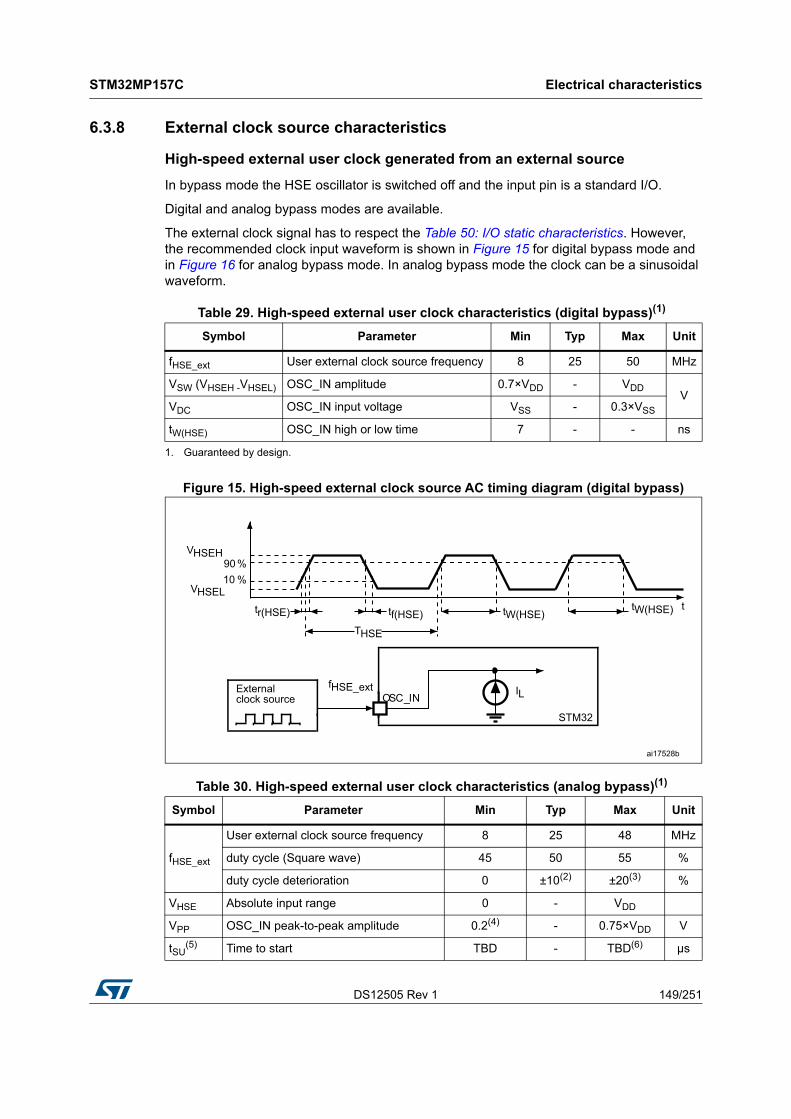
DS12505 Rev 1 149/251
STM32MP157C Electrical characteristics
234
6.3.8 External clock source characteristics
High-speed external user clock generated from an external source
In bypass mode the HSE oscillator is switched off and the input pin is a standard I/O.
Digital and analog bypass modes are available.
The external clock signal has to respect the Table 50: I/O static characteristics. However, the recommended clock input waveform is shown in Figure 15 for digital bypass mode and in Figure 16 for analog bypass mode. In analog bypass mode the clock can be a sinusoidal waveform.
Figure 15. High-speed external clock source AC timing diagram (digital bypass)
Table 29. High-speed external user clock characteristics (digital bypass)(1)
1. Guaranteed by design.
Symbol Parameter Min Typ Max Unit
fHSE_ext User external clock source frequency 8 25 50 MHz
VSW (VHSEH -VHSEL) OSC_IN amplitude 0.7×VDD - VDDV
VDC OSC_IN input voltage VSS - 0.3×VSS
tW(HSE) OSC_IN high or low time 7 - - ns
Table 30. High-speed external user clock characteristics (analog bypass)(1)
Symbol Parameter Min Typ Max Unit
fHSE_ext
User external clock source frequency 8 25 48 MHz
duty cycle (Square wave) 45 50 55 %
duty cycle deterioration 0 ±10(2) ±20(3) %
VHSE Absolute input range 0 - VDD
VPP OSC_IN peak-to-peak amplitude 0.2(4) - 0.75×VDD V
tSU(5) Time to start TBD - TBD(6) µs
ai17528b
OSC_INExternal
STM32
clock source
VHSEH
tf(HSE) tW(HSE)
IL
90 %10 %
THSE
ttr(HSE) tW(HSE)
fHSE_ext
VHSEL

Electrical characteristics STM32MP157C
150/251 DS12505 Rev 1
Figure 16. High-speed external clock source AC timing diagram (analog bypass)
Low-speed external user clock generated from an external source
In bypass mode the LSE oscillator is switched off and the input pin is a standard I/O. The external clock signal has to respect the Table 50: I/O static characteristics. However, the recommended clock input waveform is shown in Figure 17.
tr/tf(HSE)
Rise and Fall time
(10% to 90% threshold levels of the input peak-to-peak amplitude)
TBD - TBD ns
I(HSE) Power consumption - TBD(7) TBD(8) µA
1. Guaranteed by design.
2. Guaranteed by design with a square wave signal (@25 °C, VDD=3.3 V /VPP = 400 mV / VDC=1 V) where VDC is the DC component of the input signal.
3. Guaranteed by design with a square wave signal (@25 °C, VDD=1.6 V /VPP = 200 mV / VDC=0.8 V) where VDC is the DC component of the input signal.
4. minimum peak-to-peak amplitude (@25 °C, 0.1<VDC<VDD-0.1 V) where VDC is the DC component of the input signal.
5. tSU(HSE) is the startup time measured from the moment it is enabled (by software) to a stabilized analog bypass clock interface is reached. This value is measured @125 °C with 200 mV peak-to-peak amplitude.
6. Maximum start-up time is obtained @125 °C with 200 mV peak-to-peak amplitude.
7. with a sine wave signal (@25 °C, VDD=3.3 V /VPP = 400 mV / VDC=0.4 V) where VDC is the DC component of the input signal.
8. with a sine wave signal (@125 °C, VDD=3.6 V /VPP = 800 mV / VDC=1.8 V) where VDC is the DC component of the input signal.
Table 30. High-speed external user clock characteristics (analog bypass)(1)
Symbol Parameter Min Typ Max Unit
MSv47498V1
VHSE
tTHSE
VPP
STM32
OSC_INIL
fHSE_ext
tr(HSE)
90%
10%
External clock source

DS12505 Rev 1 151/251
STM32MP157C Electrical characteristics
234
Note: For information on selecting the crystal, refer to the application note AN2867 “Oscillator design guide for ST microcontrollers” available from the ST website www.st.com.
Figure 17. Low-speed external clock source AC timing diagram
High-speed external clock generated from a crystal/ceramic resonator
The high-speed external (HSE) clock can be supplied with a 8 to 48 MHz crystal/ceramic resonator oscillator. All the information given in this paragraph are based on characterization results obtained with typical external components specified in Table 32. In the application, the resonator and the load capacitors have to be placed as close as possible to the oscillator pins in order to minimize output distortion and startup stabilization time. Refer to the crystal resonator manufacturer for more details on the resonator characteristics (frequency, package, accuracy).
Table 31. Low-speed external user clock characteristics(1)
Symbol Parameter Min Typ Max Unit
fLSE_ext User external clock source frequency - 32.768 1000 kHz
VLSEH OSC32_IN input pin high level voltage 0.7×VDD - VDDV
VLSEL OSC32_IN input pin low level voltage VSS - 0.3 VDD
tw(LSEH) tw(LSEL)
OSC32_IN high or low time 250 - - ns
1. Guaranteed by design.
ai17529b
OSC32_INExternal
STM32
clock source
VLSEH
tf(LSE) tW(LSE)
IL
90%10%
TLSE
ttr(LSE) tW(LSE)
fLSE_ext
VLSEL
Table 32. 8-48 MHz HSE oscillator characteristics(1)
Symbol Parameter Operating conditions(2) Min Typ Max Unit
F Oscillator frequency - 8 - 48 MHz
RF Feedback resistor - - 200 - kΩ

Electrical characteristics STM32MP157C
152/251 DS12505 Rev 1
For CL1 and CL2, it is recommended to use high-quality external ceramic capacitors in the 5 pF to 25 pF range (typical), designed for high-frequency applications, and selected to match the requirements of the crystal or resonator (see Figure 18). CL1 and CL2 are usually the same size. The crystal manufacturer typically specifies a load capacitance which is the series combination of CL1 and CL2. The PCB and MCU pin capacitance must be included (10 pF can be used as a rough estimate of the combined pin and board capacitance) when sizing CL1 and CL2.
Note: For information on selecting the crystal, refer to the application note AN2867 “Oscillator design guide for ST microcontrollers” available from the ST website www.st.com.
Figure 18. Typical application with a 24 MHz crystal
1. REXT value depends on the crystal characteristics.
IDD(HSE) HSE current consumption
During startup(3) - - 4
mA
VDD = 3 V, Rm = 150 Ω
CL = 12 pF at 4 MHz- 0.35 -
VDD = 3 V, Rm = 120 Ω
CL = 12 pF at 16 MHz- 0.40 -
VDD = 3 V, Rm = 100 Ω
CL = 10 pF at 24 MHz- 0.45 -
VDD = 3 V, Rm = 80 Ω
CL = 8 pF at 32 MHz- 0.65 -
VDD = 3 V, Rm = 80 Ω
CL = 8 pF at 48 MHz- 0.95 -
Gmcritmax Maximum critical crystal gm Startup - - 1.5 mA/V
tSU(4) Start-up time VDD is stabilized - 2 - ms
1. Guaranteed by design.
2. Resonator characteristics given by the crystal/ceramic resonator manufacturer.
3. This consumption level occurs during the first 2/3 of the tSU(HSE) startup time.
4. tSU(HSE) is the startup time measured from the moment it is enabled (by software) to a stabilized 8 MHz oscillation is reached. This value is measured for a standard crystal resonator and it can vary significantly with the crystal manufacturer.
Table 32. 8-48 MHz HSE oscillator characteristics(1) (continued)
Symbol Parameter Operating conditions(2) Min Typ Max Unit
ai17530b
OSC_OUT
OSC_IN fHSECL1
RF
STM32
8 MHzresonator
Resonator withintegrated capacitors
Bias controlled
gain
REXT(1) CL2

DS12505 Rev 1 153/251
STM32MP157C Electrical characteristics
234
Low-speed external clock generated from a crystal/ceramic resonator
The low-speed external (LSE) clock can be supplied with a 32.768 kHz crystal/ceramic resonator oscillator. All the information given in this paragraph are based on characterization results obtained with typical external components specified in Table 33. In the application, the resonator and the load capacitors have to be placed as close as possible to the oscillator pins in order to minimize output distortion and startup stabilization time. Refer to the crystal resonator manufacturer for more details on the resonator characteristics (frequency, package, accuracy).
Note: For information on selecting the crystal, refer to the application note AN2867 “Oscillator design guide for ST microcontrollers” available from the ST website www.st.com.
Table 33. Low-speed external user clock characteristics(1)
Symbol Parameter Operating conditions(2) Min Typ Max Unit
F Oscillator frequency - - 32.768 - kHz
IDDLSE current consumption
LSEDRV[1:0] = 00, Low drive capability
- 290 -
nA
LSEDRV[1:0] = 01, Medium Low drive capability
- 390 -
LSEDRV[1:0] = 10, Medium high drive capability
- 550 -
LSEDRV[1:0] = 11, High drive capability
- 900 -
GmcritmaxMaximum critical crystal gm
LSEDRV[1:0] = 00, Low drive capability
- - 0.5
µA/V
LSEDRV[1:0] = 01, Medium Low drive capability
- - 0.75
LSEDRV[1:0] = 10, Medium high drive capability
- - 1.7
LSEDRV[1:0] = 11, High drive capability
- - 2.7
tSU(3) Startup time VDD is stabilized - 2 - s
1. Guaranteed by design.
2. Refer to the note and caution paragraphs below the table, and to the application note AN2867 “Oscillator design guide for ST microcontrollers.
3. tSU is the startup time measured from the moment it is enabled (by software) to a stabilized 32.768 k Hz oscillation is reached. This value is measured for a standard crystal resonator and it can vary significantly with the crystal manufacturer.

Electrical characteristics STM32MP157C
154/251 DS12505 Rev 1
Figure 19. Typical application with a 32.768 kHz crystal
1. An external resistor is not required between OSC32_IN and OSC32_OUT and it is forbidden to add one.
6.3.9 Internal clock source characteristics
The parameters given in Table 34, Table 35 and Table 36 are derived from tests performed under ambient temperature and VDD supply voltage conditions summarized in Table 13: General operating conditions.
64 MHz high-speed internal RC oscillator (HSI)
ai17531b
OSC32_OUT
OSC32_IN fLSECL1
RF
STM32
32.768 kHzresonator
Resonator withintegrated capacitors
Bias controlled
gain
CL2
Table 34. HSI oscillator characteristics(1)
Symbol Parameter Conditions Min Typ Max Unit
fHSI HSI frequency VDD = 3.3 V, TJ = 30 °C TBD 64 TBD MHz
TRIM HSI user trimming step
Trimming is not a multiple of 32
TBD 0.33 TBD
%
Trimming is 128, 256 and 384
TBD -2.43 TBD
Trimming is 64, 192, 320 and 448
TBD -0.70 TBD
Other trimming are a multiple of 32 (not including multiple of 64 and 128)
TBD -0.30 TBD
DuCy(HSI) Duty Cycle - 45 - 55 %
∆VDD (HSI)HSI oscillator frequency drift over VDD (reference is 3.3 V)
VDD = 1.71 to 3.6 V -0.12 - 0.03 %
∆TEMP (HSI)
HSI oscillator frequency drift over temperature (reference is 64 MHz) With Temperature Trimming
TJ = -20 to 110 °C TBD - TBD%
TJ = -40 to 125 °C -2.62 - 2.08
∆TEMP_NOT
RIM (HSI)
HSI oscillator frequency drift over temperature (reference is 64 MHz) Without Temperature Trimming
TJ = -20 to 110 °C TBD - TBD%
T J =-40 to 125 °C -4 - 2.5
tsu(HSI)HSI oscillator start-up time (Time between Enable rising and First output clock edge.)
- - 1.47 TBD µs
tstab(HSI) HSI oscillator stabilization time at 1% of target frequency - 3 TBD µs
IDD(HSI) HSI oscillator power consumption - - 300 TBD µA
DS12505 Rev 1 155/251
STM32MP157C Electrical characteristics
234
4 MHz low-power internal RC oscillator (CSI)
40 kHz low-speed internal (LSI) RC oscillator
1. Guaranteed by design unless otherwise specified.
Table 35. CSI oscillator characteristics(1)
Symbol Parameter Conditions Min Typ Max Unit
fCSI CSI frequency VDD = 3.3 V, TJ = 30 °C TBD(2) 4 TBD(2) MHz
TRIM Trimming step
Trimming code is not a multiple of 16
- 0.85 TBD %
Trimming code is a multiple of 16
TBD -3.5 TBD
DuCy(CSI) Duty Cycle - TBD 54 TBD %
∆VDD (CSI) + ∆TEMP (CSI)
CSI oscillator frequency drift over VDD & drift over temperature
VDD = 1.71 to 3.6 V
TJ = 0 to 85 °CTBD ±1.43(3) TBD %
tsu(CSI) CSI oscillator startup time - - 2 TBD µs
tstab(CSI)CSI oscillator stabilization time (to reach ±5% of fCSI)
TJ = 0 to 85 °C - 5 TBD cycle
IDD(CSI) CSI oscillator power consumption - - 30 TBD µA
1. Guaranteed by design.
2. Guaranteed by test in production.
3. Guaranteed by characterization results.
Table 36. LSI oscillator characteristics
Symbol Parameter Conditions Min Typ Max Unit
fLSI LSI frequency
TJ = 25 °C,
VDD = 3.3 V
(after calibration)
TBD 32 TBD
kHz
TJ = 0 to 110 °C, VDD = 1.71 to 3.6 V
TBD 32 TBD
TJ = -40 to 110 °C, VDD = 1.71 to 3.6 V
TBD 32 TBD
TJ = -40 to 125 °C, VDD = 1.71 to 3.6 V (after calibration)
TBD 32 TBD
tsu(LSI)(1)
LSI oscillator startup time (Time between Enable rising and First output clock edge.)
- - 64 TBD
µs
tstab(LSI)(1) LSI oscillator stabilization time
(5% of final value)- - 110 TBD
IDD(LSI)(1) LSI oscillator power
consumption- - 120 TBD nA
Electrical characteristics STM32MP157C
156/251 DS12505 Rev 1
6.3.10 PLL characteristics
The parameters given in Table 37, Table 38, Table 39, Table 40 are derived from tests performed under temperature and VDD supply voltage conditions summarized in Table 13: General operating conditions.
PLL1_1600, PLL2_1600 characteristics
1. Guaranteed by design.
Table 37. PLL1_1600, PLL2_1600 characteristics(1)
Symbol Parameter Conditions Min Typ Max Unit
fPLL_IN
PLL input clock Normal mode and Sigma delta mode 8 - 16 MHz
PLL input clock duty cycle
- 10 - 90 %
fPLL_P_Q_R_
OUT
PLL P,Q,R multiplier output clock
- 3.125 - 800(2) MHz
PLL P,Q,R clock duty cycle
Division by 1 45 50 55
%
Even divisions
(N multiple of 2)45 50 55
Odd divisions
(N not multiple of 2)
[100, (N+1)/2N] - 5
[100, (N+1)/
2N]
[100, (N+1)/2N] +
5
fVCO_OUT PLL VCO output - 400 - 800 MHz
tLOCK PLL lock timeNormal mode - 50 150
µsSigma-delta mode (CKIN ≥ 8 MHz) - 65 170
ALOCK
Lock Accuracy
(Ratio VCO frequency versus target frequency at lock)
- - - ±2 %

DS12505 Rev 1 157/251
STM32MP157C Electrical characteristics
234
PLL3_800, PLL4_800 characteristics
Jitter
RMS cycle-to-cycle jitter
fPLL_P_Q_R_OUT division = 1 to 16
Without Fractional mode
VCO = 400 MHz - 18(3) -
±ps
VCO = 533 MHz - 14(3) -
VCO = 800 MHz - 12(3) -
fPLL_P_Q_R_OUT division = 1 to 16
With Fractional mode
VCO = 533 MHz - 20(3) -
VCO = 800 MHz - 18(3) -
RMS period jitter
fPLL_P_Q_R_OUT division = 1 to 16
Without Fractional mode
VCO = 400 MHz - 16(3) -
±ps
VCO = 533 MHz - 12(3) -
VCO = 800 MHz - 10(3) -
fPLL_P_Q_R_OUT division = 1 to 16
With Fractional mode
VCO = 533 MHz - 16(3) -
VCO = 800 MHz - 15(3) -
Long term jitter
fPLL_P_Q_R_OUT division = 1 to 16
fPLL_IN = 8 MHz
Without Fractional mode
VCO = 400 MHz - 225(4) -
ps
VCO = 533 MHz - 200(4) -
VCO = 800 MHz - 100(4) -
fPLL_P_Q_R_OUT division = 1 to 16
fPLL_IN = 8 MHz
With Fractional mode
VCO = 400 MHz - 350(4) -
VCO = 533 MHz - 250(4) -
VCO = 800 MHz - 150(4) -
IVDD_PLL(2)
PLL power consumption on VDD_PLL (Analog)
VCO freq = 800 MHz - 930 -µA
VCO freq = 400 MHz - 560 -
IVDDCORE(2)
PLL power consumption on VDDCORE (Digital)
VCO freq = 800 MHzVDDCORE=1.1 V - 4200 -
μAVDDCORE=1.26 V - 5200 -
VCO freq = 400 MHzVDDCORE=1.1 V - 2100 -
VDDCORE=1.26 V - 2600 -
1. Guaranteed by design unless otherwise specified.
2. Guaranteed by characterization results.
3. Measured on DDR high speed IO.
4. Measured on DDR high speed IO for 10000 output clock cycles.
Table 37. PLL1_1600, PLL2_1600 characteristics(1) (continued)
Symbol Parameter Conditions Min Typ Max Unit
Table 38. PLL3_800, PLL4_800 characteristics(1)
Symbol Parameter Conditions Min Typ Max Unit
fPLL_IN
PLL input clock Normal mode 4 - 16MHz
Sigma delta mode 8 16
PLL input clock duty cycle
- 10 - 90 %

Electrical characteristics STM32MP157C
158/251 DS12505 Rev 1
fPLL_P_Q_R_
OUT
PLL P,Q,R multiplier output clock
- 3.125 - 800(2) MHz
PLL P,Q,R clock duty cycle
Even divisions
(N multiple of 2)45 50 55
%Odd divisions
(N not multiple of 2)
[100, (N+1)/2N] - 5
[100, (N+1)/
2N]
[100, (N+1)/2N] +
5
fVCO_OUT PLL VCO output - 400 - 800 MHz
tLOCK PLL lock timeNormal mode 15 50 150
µsSigma-delta mode (CKIN ≥ 8 MHz) 25 65 170
ALOCK
Lock accuracy
(Ratio VCO frequency versus target frequency at lock)
- - - ±2 %
Jitter
RMS cycle-to-cycle jitter
fPLL_P_Q_R_OUT division = 25 to 100
Without Fractional mode
VCO = 400 MHz - 80(3) -
±ps
VCO = 600 MHz - 50(3) -
VCO = 800 MHz - 45(3) -
fPLL_P_Q_R_OUT division = 25 to 100
With Fractional mode
VCO = 600 MHz - 65(3) -
VCO = 800 MHz - 60(3) -
RMS period jitter
fPLL_P_Q_R_OUT division = 25 to 100
Without Fractional mode
VCO = 400 MHz - 75(3) -
±ps
VCO = 600 MHz - 38(3) -
VCO = 800 MHz - 30(3) -
fPLL_P_Q_R_OUT division = 25 to 100
With Fractional mode
VCO = 600 MHz - 55(3) -
VCO = 800 MHz - 50(3) -
Long term jitter
fPLL_P_Q_R_OUT division = 25 to 100
fPLL_IN = 8 MHz
Without Fractional mode
VCO = 400 MHz - 225(4) -
ps
VCO = 600 MHz - 150(4) -
VCO = 800 MHz - 125(4) -
fPLL_P_Q_R_OUT division = 25 to 100
fPLL_IN = 8 MHz
With Fractional mode
VCO = 400 MHz - 300(4) -
VCO = 600 MHz - 200(4) -
VCO = 800 MHz - 150(4) -
IVDD_PLL(2)
PLL power consumption on VDD_PLL (Analog)
VCO freq = 800 MHz - 600 -µA
VCO freq = 400 MHz - 320 -
Table 38. PLL3_800, PLL4_800 characteristics(1) (continued)
Symbol Parameter Conditions Min Typ Max Unit

DS12505 Rev 1 159/251
STM32MP157C Electrical characteristics
234
PLL_USB (2880 MHz) characteristics
PLL_DSI (2000 MHz) characteristics
IVDDCORE(2)
PLL power consumption on VDDCORE (Digital)
VCO freq = 800 MHz
VDDCORE = 1.1 V - 1960 -
µA
VDDCORE = 1.26 V
- 2340 -
VCO freq = 400 MHz
VDDCORE = 1.1 V - 970 -
VDDCORE = 1.26 V
- 1210 -
1. Guaranteed by design unless otherwise specified.
2. Guaranteed by characterization results.
3. Measured on GPIO.
4. Measured on GPIO for 10000 output clock cycles.
Table 38. PLL3_800, PLL4_800 characteristics(1) (continued)
Symbol Parameter Conditions Min Typ Max Unit
Table 39. USB_PLL characteristics(1)
Symbol Parameter Condition Min Typ Max Unit
fPLL_IN PLL input clock 19.2 - 38.4 MHz
fPLL_INFIN PFD input clock 19.2 - 38.4 MHz
fPLL_OUT PLL multiplier output clock - 480 - MHz
fVCO_OUT PLL VCO output - 2880 - MHz
tLOCK PLL lock time - - 100 µs
tPDN PLL power down time 10 - - µs
IDDA1V1_R
EG(PLL)
PLL power consumption on VDDA1V1_REG (internal connection)
PLL in power down - TBD TBDµA
fVCO_OUT = 2880 MHz - TBD TBD
IDDA1V8_R
EG(PLL)
PLL power consumption on VDDA1V8_REG (internal connection)
PLL in power down - - TBDµA
fVCO_OUT = 2880 MHz - TBD TBD
1. Guaranteed by characterization results.
Table 40. DSI_PLL characteristics(1)
Symbol Parameter Condition Min Typ Max Unit
fPLL_IN PLL input clock 8 - 200 MHz
fPLL_INFIN PFD input clock 8 - 50 MHz
fPLL_OUT PLL multiplier output clock 62.5 - 1000 MHz
fVCO_OUT PLL VCO output 1000 - 2000 MHz
tLOCK PLL lock time - - 100 µs
tPDN PLL power down time 5 - - µs

Electrical characteristics STM32MP157C
160/251 DS12505 Rev 1
6.3.11 PLL spread spectrum clock generation (SSCG) characteristics
The spread spectrum clock generation (SSCG) feature allows the reduction of electromagnetic interferences (see Table 46: EMI characteristics). It is available only on the PLL1_1600, PLL2_1600, PLL3_800 and PLL4_800.
Equation 1
The frequency modulation period (MODEPER) is given by the equation below:
fPLL_IN and fMod must be expressed in Hz.
As an example:
If fPLL_IN = 1 MHz, and fMOD = 1 kHz, the modulation depth (MODEPER) is given by equation 1:
Equation 2
Equation 2 allows the increment step (INCSTEP) calculation:
fVCO_OUT must be expressed in MHz.
With a modulation depth (md) = ±2% (4% peak-to-peak), and PLLN = 240 (in MHz):
An amplitude quantization error may be generated because the linear modulation profile is obtained by taking the quantized values (rounded to the nearest integer) of MODPER and
IDD1V2_DSI
_REG(PLL)
PLL power consumption on VDD1V2_DSI_REG (internal connection)
PLL in power down - TBD TBD µA
fVCO_OUT = 1000 MHz - TBD -mA
fVCO_OUT = 2000 MHz - TBD TBD
1. Guaranteed by characterization results.
Table 40. DSI_PLL characteristics(1) (continued)
Symbol Parameter Condition Min Typ Max Unit
Table 41. SSCG parameters constraint
Symbol Parameter Min Typ Max(1) Unit
fMod Modulation frequency 20 - 60 kHz
md Peak modulation depth 0.25 - 2 %
MODEPER * INCSTEP - - - 215-1 -
1. Guaranteed by design.
MODEPER round fPLL_IN 4 fMod×( )⁄[ ]=
MODEPER round 106
4 103×( )⁄[ ] 250= =
INCSTEP round 215
1–( ) md PLLN××( ) 100 5× MODEPER×( )⁄[ ]=
INCSTEP round 215
1–( ) 2 240××( ) 100 5× 250×( )⁄[ ] 126md(quantitazed)%= =
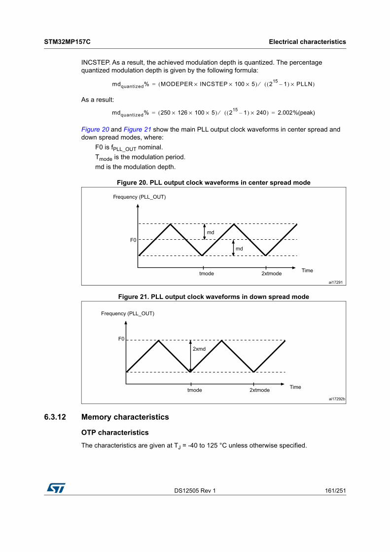
DS12505 Rev 1 161/251
STM32MP157C Electrical characteristics
234
INCSTEP. As a result, the achieved modulation depth is quantized. The percentage quantized modulation depth is given by the following formula:
As a result:
Figure 20 and Figure 21 show the main PLL output clock waveforms in center spread and down spread modes, where:
F0 is fPLL_OUT nominal.
Tmode is the modulation period.
md is the modulation depth.
Figure 20. PLL output clock waveforms in center spread mode
Figure 21. PLL output clock waveforms in down spread mode
6.3.12 Memory characteristics
OTP characteristics
The characteristics are given at TJ = -40 to 125 °C unless otherwise specified.
mdquantized% MODEPER INCSTEP× 100× 5×( ) 215
1–( ) PLLN×( )⁄=
mdquantized% 250 126× 100× 5×( ) 215
1–( ) 240×( )⁄ 2.002%(peak)= =
Frequency (PLL_OUT)
Time
F0
tmode 2xtmode
md
ai17291
md
Frequency (PLL_OUT)
Time
F0
tmode 2xtmode
2xmd
ai17292b

Electrical characteristics STM32MP157C
162/251 DS12505 Rev 1
DDR characteristics
DDR3L I/O DC specifications
The following table provides input and output DC threshold values and on-die-termination (ODT) recommended values. The conditions for the output threshold values are un-terminated outputs loaded with 1 pF capacitor load. The ODT values are measured after impedance calibration.
Table 42. OTP characteristics
Symbol Parameter Conditions Min Max Unit
IVDDCORE OTP consumption on VDDCORE
Programming - 450 µA
Reading - 490 µA
PowerDown - 4.2 µA
IVDD OTP consumption on VDD
Programming - 10000 µA
Reading - 2200 µA
PowerDown - 1 µA
FOTP (1) OTP operating Frequency - - 67 MHz
NB_CYCLE (2) Maximum number of reading cycles - - 500 Million
1. Guaranteed by design.
2. Guaranteed by characterization results.
Table 43. DC specifications – DDR3L mode(1)
Symbol Parameter Min Typ Max Unit
VIH(DC) DC input voltage high VREF + 0.09 - VDDQ V
VIL(DC) DC input voltage low VSSQ - 0.3 - VREF - 0.09 V
VOH DC output logic high 0.8 × VDDQ - - V
VOL DC output logic low - - 0.2 × VDDQ V
RTT Input termination resistance (ODT) to VDDQ/21005436
1206040
1406644
Ω
ILS Input leakage current, SSTL mode, unterminated - 0.01 4.8 μA
1. Guaranteed by design.

DS12505 Rev 1 163/251
STM32MP157C Electrical characteristics
234
LPDDR2, LPDDR3 I/O DC specifications
The following table provides input and output DC threshold values. The conditions for the output threshold values are un-terminated outputs loaded with 1 pF capacitor load.
6.3.13 EMC characteristics
Susceptibility tests are performed on a sample basis during device characterization.
Functional EMS (electromagnetic susceptibility)
While a simple application is executed on the device (toggling 2 LEDs through I/O ports). the device is stressed by two electromagnetic events until a failure occurs. The failure is indicated by the LEDs:
• Electrostatic discharge (ESD) (positive and negative) is applied to all device pins until a functional disturbance occurs. This test is compliant with the IEC 61000-4-2 standard.
• FTB: a burst of fast transient voltage (positive and negative) is applied to VDD and VSS through a 100 pF capacitor, until a functional disturbance occurs. This test is compliant with the IEC 61000-4-4 standard.
A device reset allows normal operations to be resumed.
The test results are given in Table 45. They are based on the EMS levels and classes defined in application note AN1709 available from the ST website www.st.com.
As a consequence, it is recommended to add a serial resistor (1 kΩ) located as close as possible to the MCU to the pins exposed to noise (connected to tracks longer than 50 mm on PCB).
Table 44. DC specifications – DDR3L mode(1)
Symbol Parameter Min Typ Max Unit
VIH(DC) DC input voltage high VREF + 0.13 - VDDQ V
VIL(DC) DC input voltage low VSSQ - VREF - 0.13 V
VOH DC output logic high 0.9 × VDDQ - - V
VOL DC output logic low - - 0.1 × VDDQ V
ILEAK Input leakage current - 0.01 4.51 μA
1. Guaranteed by design.
Table 45. EMS characteristics
Symbol Parameter ConditionsLevel/Class
VFESDVoltage limits to be applied on any I/O pin to induce a functional disturbance
VDD = 3.3 V, VDDCORE = 1.2 V, TA = +25 °C,
LFBGA448, Fmpuss_ck = 648 MHz,
Fmcu_ck = 209 MHz, M4 core not running,
conforms to IEC 61000-4-2
2B
VFTB
Fast transient voltage burst limits to be applied through 100 pF on VDD and VSS pins to induce a functional disturbance
5A
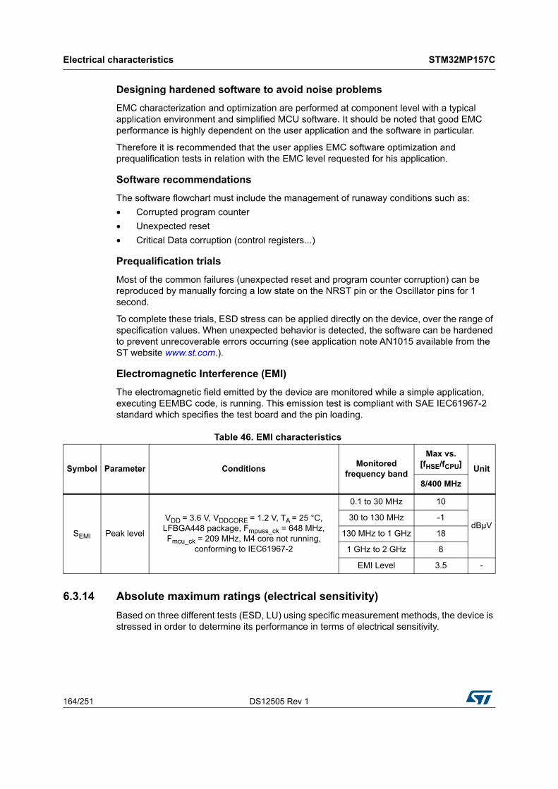
Electrical characteristics STM32MP157C
164/251 DS12505 Rev 1
Designing hardened software to avoid noise problems
EMC characterization and optimization are performed at component level with a typical application environment and simplified MCU software. It should be noted that good EMC performance is highly dependent on the user application and the software in particular.
Therefore it is recommended that the user applies EMC software optimization and prequalification tests in relation with the EMC level requested for his application.
Software recommendations
The software flowchart must include the management of runaway conditions such as:
• Corrupted program counter
• Unexpected reset
• Critical Data corruption (control registers...)
Prequalification trials
Most of the common failures (unexpected reset and program counter corruption) can be reproduced by manually forcing a low state on the NRST pin or the Oscillator pins for 1 second.
To complete these trials, ESD stress can be applied directly on the device, over the range of specification values. When unexpected behavior is detected, the software can be hardened to prevent unrecoverable errors occurring (see application note AN1015 available from the ST website www.st.com.).
Electromagnetic Interference (EMI)
The electromagnetic field emitted by the device are monitored while a simple application, executing EEMBC code, is running. This emission test is compliant with SAE IEC61967-2 standard which specifies the test board and the pin loading.
6.3.14 Absolute maximum ratings (electrical sensitivity)
Based on three different tests (ESD, LU) using specific measurement methods, the device is stressed in order to determine its performance in terms of electrical sensitivity.
Table 46. EMI characteristics
Symbol Parameter ConditionsMonitored
frequency band
Max vs. [fHSE/fCPU] Unit
8/400 MHz
SEMI Peak level
VDD = 3.6 V, VDDCORE = 1.2 V, TA = 25 °C, LFBGA448 package, Fmpuss_ck = 648 MHz, Fmcu_ck = 209 MHz, M4 core not running,
conforming to IEC61967-2
0.1 to 30 MHz 10
dBµV30 to 130 MHz -1
130 MHz to 1 GHz 18
1 GHz to 2 GHz 8
EMI Level 3.5 -

DS12505 Rev 1 165/251
STM32MP157C Electrical characteristics
234
Electrostatic discharge (ESD)
Electrostatic discharges (a positive then a negative pulse) are applied to the pins of each sample according to each pin combination. This test conforms to the ANSI/ESDA/JEDEC JS-001 and ANSI/ESDA/JEDEC JS-002 standards.
Static latchup
Two complementary static tests are required on six parts to assess the latchup performance:
• A supply overvoltage is applied to each power supply pin
• A current injection is applied to each input, output and configurable I/O pin
These tests are compliant with JESD78 IC latchup standard.
6.3.15 I/O current injection characteristics
As a general rule, a current injection to the I/O pins, due to external voltage below VSS or above VDD (for standard, 3.3 V-capable I/O pins) should be avoided during the normal product operation. However, in order to give an indication of the robustness of the device in cases when an abnormal injection accidentally happens, susceptibility tests are performed on a sample basis during the device characterization.
Functional susceptibility to I/O current injection
While a simple application is executed on the device, the device is stressed by injecting current into the I/O pins programmed in floating input mode. While current is injected into the I/O pin, one at a time, the device is checked for functional failures.
The failure is indicated by an out of range parameter: ADC error above a certain limit (higher than 5 LSB TUE), out of conventional limits of induced leakage current on adjacent pins (out of –5 µA/+0 µA range), or other functional failure (for example reset, oscillator frequency deviation).
The following tables are the compilation of the SIC1/SIC2 and functional ESD results.
Table 47. ESD absolute maximum ratings
Symbol Ratings Conditions Packages ClassMaximum value(1) Unit
VESD(HBM)
Electrostatic discharge voltage (human body model)
TA = +25 °C conforming to ANSI/ESDA/JEDEC JS-001
All 1C 1000
V
VESD(CDM)
Electrostatic discharge voltage (charge device model)
TA = +25 °C conforming to ANSI/ESDA/JEDEC JS-002
All C1 250
1. Guaranteed by characterization results.
Table 48. Electrical sensitivities
Symbol Parameter Conditions Class
LU Static latchup class TA = +25 °C conforming to JESD78 II level A
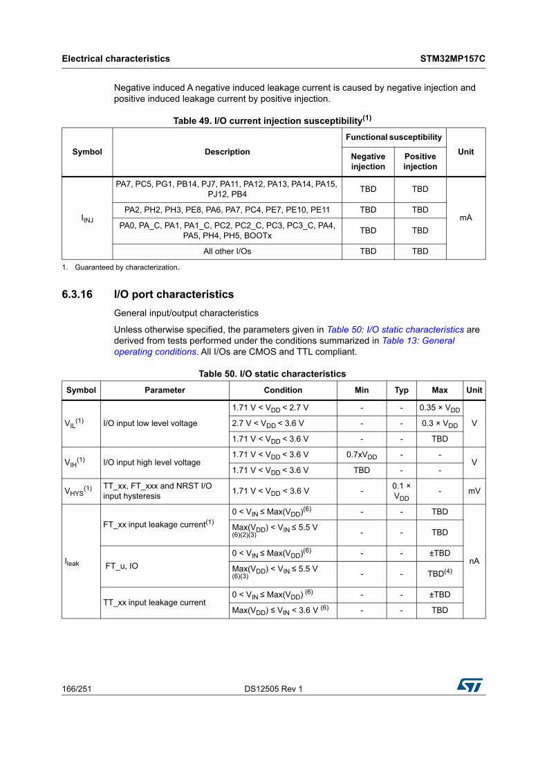
Electrical characteristics STM32MP157C
166/251 DS12505 Rev 1
Negative induced A negative induced leakage current is caused by negative injection and positive induced leakage current by positive injection.
6.3.16 I/O port characteristics
General input/output characteristics
Unless otherwise specified, the parameters given in Table 50: I/O static characteristics are derived from tests performed under the conditions summarized in Table 13: General operating conditions. All I/Os are CMOS and TTL compliant.
Table 49. I/O current injection susceptibility(1)
Symbol Description
Functional susceptibility
UnitNegative injection
Positive injection
IINJ
PA7, PC5, PG1, PB14, PJ7, PA11, PA12, PA13, PA14, PA15, PJ12, PB4
TBD TBD
mAPA2, PH2, PH3, PE8, PA6, PA7, PC4, PE7, PE10, PE11 TBD TBD
PA0, PA_C, PA1, PA1_C, PC2, PC2_C, PC3, PC3_C, PA4, PA5, PH4, PH5, BOOTx
TBD TBD
All other I/Os TBD TBD
1. Guaranteed by characterization.
Table 50. I/O static characteristics
Symbol Parameter Condition Min Typ Max Unit
VIL(1) I/O input low level voltage
1.71 V < VDD < 2.7 V - - 0.35 × VDD
V2.7 V < VDD < 3.6 V - - 0.3 × VDD
1.71 V < VDD < 3.6 V - - TBD
VIH(1) I/O input high level voltage
1.71 V < VDD < 3.6 V 0.7xVDD - -V
1.71 V < VDD < 3.6 V TBD - -
VHYS(1) TT_xx, FT_xxx and NRST I/O
input hysteresis1.71 V < VDD < 3.6 V -
0.1 × VDD
- mV
Ileak
FT_xx input leakage current(1)
0 < VIN ≤ Max(VDD)(6) - - TBD
nA
Max(VDD) < VIN ≤ 5.5 V (6)(2)(3) - - TBD
FT_u, IO
0 < VIN ≤ Max(VDD)(6) - - ±TBD
Max(VDD) < VIN ≤ 5.5 V (6)(3) - - TBD(4)
TT_xx input leakage current0 < VIN ≤ Max(VDD) (6) - - ±TBD
Max(VDD) ≤ VIN < 3.6 V (6) - - TBD
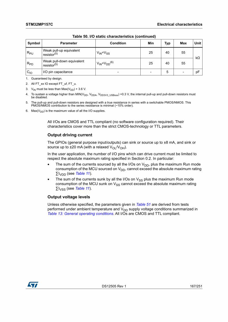
DS12505 Rev 1 167/251
STM32MP157C Electrical characteristics
234
All I/Os are CMOS and TTL compliant (no software configuration required). Their characteristics cover more than the strict CMOS-technology or TTL parameters.
Output driving current
The GPIOs (general purpose input/outputs) can sink or source up to ±8 mA, and sink or source up to ±20 mA (with a relaxed VOL/VOH).
In the user application, the number of I/O pins which can drive current must be limited to respect the absolute maximum rating specified in Section 0.2. In particular:
• The sum of the currents sourced by all the I/Os on VDD, plus the maximum Run mode consumption of the MCU sourced on VDD, cannot exceed the absolute maximum rating ∑IVDD (see Table 11).
• The sum of the currents sunk by all the I/Os on VSS plus the maximum Run mode consumption of the MCU sunk on VSS cannot exceed the absolute maximum rating ∑IVSS (see Table 11).
Output voltage levels
Unless otherwise specified, the parameters given in Table 51 are derived from tests performed under ambient temperature and VDD supply voltage conditions summarized in Table 13: General operating conditions. All I/Os are CMOS and TTL compliant.
RPUWeak pull-up equivalent resistor(5) VIN=VSS 25 40 55
kΩ
RPDWeak pull-down equivalent resistor(5) VIN=VDD
(6) 25 40 55
CIO I/O pin capacitance - - 5 - pF
1. Guaranteed by design.
2. All FT_xx IO except FT_uf, FT_u.
3. VIN must be less than Max(VDD) + 3.6 V.
4. To sustain a voltage higher than MIN(VDD, VDDA, VDD3V3_USBxxx) +0.3 V, the internal pull-up and pull-down resistors must be disabled.
5. The pull-up and pull-down resistors are designed with a true resistance in series with a switchable PMOS/NMOS. This PMOS/NMOS contribution to the series resistance is minimal (~10% order).
6. Max(VDD) is the maximum value of all the I/O supplies.
Table 50. I/O static characteristics (continued)
Symbol Parameter Condition Min Typ Max Unit
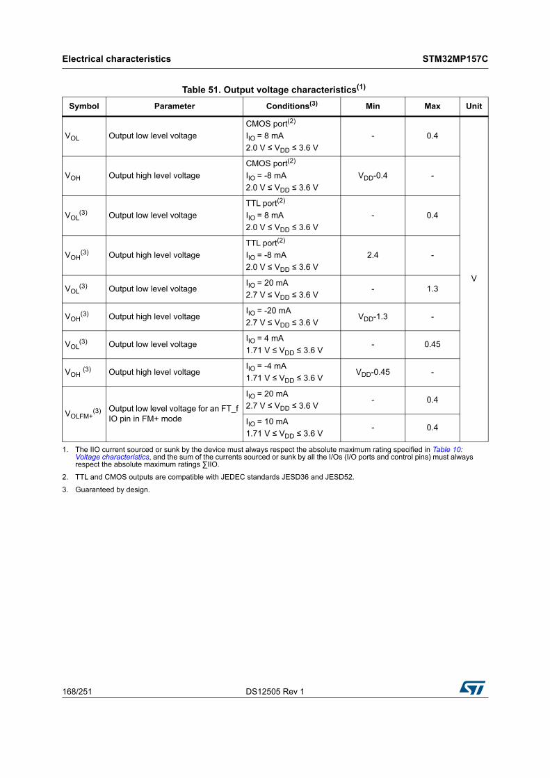
Electrical characteristics STM32MP157C
168/251 DS12505 Rev 1
Table 51. Output voltage characteristics(1)
Symbol Parameter Conditions(3) Min Max Unit
VOL Output low level voltage
CMOS port(2)
IIO = 8 mA
2.0 V ≤ VDD ≤ 3.6 V
- 0.4
V
VOH Output high level voltage
CMOS port(2)
IIO = -8 mA
2.0 V ≤ VDD ≤ 3.6 V
VDD-0.4 -
VOL(3) Output low level voltage
TTL port(2)
IIO = 8 mA
2.0 V ≤ VDD ≤ 3.6 V
- 0.4
VOH(3) Output high level voltage
TTL port(2)
IIO = -8 mA
2.0 V ≤ VDD ≤ 3.6 V
2.4 -
VOL(3) Output low level voltage
IIO = 20 mA
2.7 V ≤ VDD ≤ 3.6 V- 1.3
VOH(3) Output high level voltage
IIO = -20 mA
2.7 V ≤ VDD ≤ 3.6 VVDD-1.3 -
VOL(3) Output low level voltage
IIO = 4 mA
1.71 V ≤ VDD ≤ 3.6 V- 0.45
VOH (3) Output high level voltageIIO = -4 mA
1.71 V ≤ VDD ≤ 3.6 VVDD-0.45 -
VOLFM+(3) Output low level voltage for an FT_f
IO pin in FM+ mode
IIO = 20 mA
2.7 V ≤ VDD ≤ 3.6 V- 0.4
IIO = 10 mA
1.71 V ≤ VDD ≤ 3.6 V- 0.4
1. The IIO current sourced or sunk by the device must always respect the absolute maximum rating specified in Table 10: Voltage characteristics, and the sum of the currents sourced or sunk by all the I/Os (I/O ports and control pins) must always respect the absolute maximum ratings ∑IIO.
2. TTL and CMOS outputs are compatible with JEDEC standards JESD36 and JESD52.
3. Guaranteed by design.
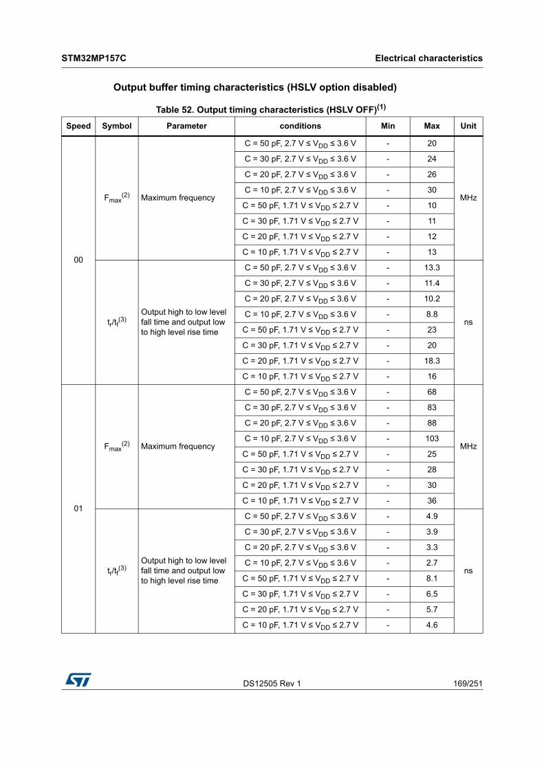
DS12505 Rev 1 169/251
STM32MP157C Electrical characteristics
234
Output buffer timing characteristics (HSLV option disabled)
Table 52. Output timing characteristics (HSLV OFF)(1)
Speed Symbol Parameter conditions Min Max Unit
00
Fmax(2) Maximum frequency
C = 50 pF, 2.7 V ≤ VDD ≤ 3.6 V - 20
MHz
C = 30 pF, 2.7 V ≤ VDD ≤ 3.6 V - 24
C = 20 pF, 2.7 V ≤ VDD ≤ 3.6 V - 26
C = 10 pF, 2.7 V ≤ VDD ≤ 3.6 V - 30
C = 50 pF, 1.71 V ≤ VDD ≤ 2.7 V - 10
C = 30 pF, 1.71 V ≤ VDD ≤ 2.7 V - 11
C = 20 pF, 1.71 V ≤ VDD ≤ 2.7 V - 12
C = 10 pF, 1.71 V ≤ VDD ≤ 2.7 V - 13
tr/tf(3)
Output high to low level fall time and output low to high level rise time
C = 50 pF, 2.7 V ≤ VDD ≤ 3.6 V - 13.3
ns
C = 30 pF, 2.7 V ≤ VDD ≤ 3.6 V - 11.4
C = 20 pF, 2.7 V ≤ VDD ≤ 3.6 V - 10.2
C = 10 pF, 2.7 V ≤ VDD ≤ 3.6 V - 8.8
C = 50 pF, 1.71 V ≤ VDD ≤ 2.7 V - 23
C = 30 pF, 1.71 V ≤ VDD ≤ 2.7 V - 20
C = 20 pF, 1.71 V ≤ VDD ≤ 2.7 V - 18.3
C = 10 pF, 1.71 V ≤ VDD ≤ 2.7 V - 16
01
Fmax(2) Maximum frequency
C = 50 pF, 2.7 V ≤ VDD ≤ 3.6 V - 68
MHz
C = 30 pF, 2.7 V ≤ VDD ≤ 3.6 V - 83
C = 20 pF, 2.7 V ≤ VDD ≤ 3.6 V - 88
C = 10 pF, 2.7 V ≤ VDD ≤ 3.6 V - 103
C = 50 pF, 1.71 V ≤ VDD ≤ 2.7 V - 25
C = 30 pF, 1.71 V ≤ VDD ≤ 2.7 V - 28
C = 20 pF, 1.71 V ≤ VDD ≤ 2.7 V - 30
C = 10 pF, 1.71 V ≤ VDD ≤ 2.7 V - 36
tr/tf(3)
Output high to low level fall time and output low to high level rise time
C = 50 pF, 2.7 V ≤ VDD ≤ 3.6 V - 4.9
ns
C = 30 pF, 2.7 V ≤ VDD ≤ 3.6 V - 3.9
C = 20 pF, 2.7 V ≤ VDD ≤ 3.6 V - 3.3
C = 10 pF, 2.7 V ≤ VDD ≤ 3.6 V - 2.7
C = 50 pF, 1.71 V ≤ VDD ≤ 2.7 V - 8.1
C = 30 pF, 1.71 V ≤ VDD ≤ 2.7 V - 6.5
C = 20 pF, 1.71 V ≤ VDD ≤ 2.7 V - 5.7
C = 10 pF, 1.71 V ≤ VDD ≤ 2.7 V - 4.6
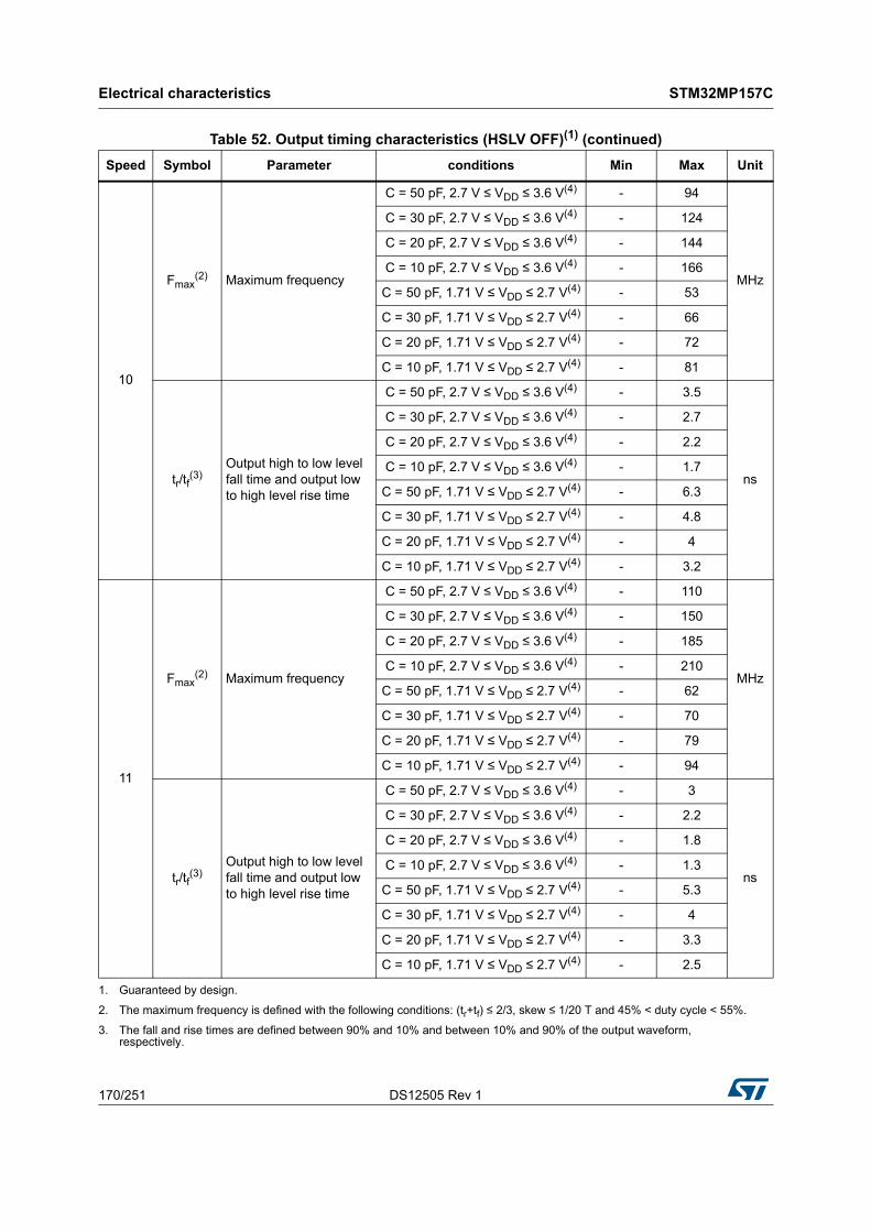
Electrical characteristics STM32MP157C
170/251 DS12505 Rev 1
10
Fmax(2) Maximum frequency
C = 50 pF, 2.7 V ≤ VDD ≤ 3.6 V(4) - 94
MHz
C = 30 pF, 2.7 V ≤ VDD ≤ 3.6 V(4) - 124
C = 20 pF, 2.7 V ≤ VDD ≤ 3.6 V(4) - 144
C = 10 pF, 2.7 V ≤ VDD ≤ 3.6 V(4) - 166
C = 50 pF, 1.71 V ≤ VDD ≤ 2.7 V(4) - 53
C = 30 pF, 1.71 V ≤ VDD ≤ 2.7 V(4) - 66
C = 20 pF, 1.71 V ≤ VDD ≤ 2.7 V(4) - 72
C = 10 pF, 1.71 V ≤ VDD ≤ 2.7 V(4) - 81
tr/tf(3)
Output high to low level fall time and output low to high level rise time
C = 50 pF, 2.7 V ≤ VDD ≤ 3.6 V(4) - 3.5
ns
C = 30 pF, 2.7 V ≤ VDD ≤ 3.6 V(4) - 2.7
C = 20 pF, 2.7 V ≤ VDD ≤ 3.6 V(4) - 2.2
C = 10 pF, 2.7 V ≤ VDD ≤ 3.6 V(4) - 1.7
C = 50 pF, 1.71 V ≤ VDD ≤ 2.7 V(4) - 6.3
C = 30 pF, 1.71 V ≤ VDD ≤ 2.7 V(4) - 4.8
C = 20 pF, 1.71 V ≤ VDD ≤ 2.7 V(4) - 4
C = 10 pF, 1.71 V ≤ VDD ≤ 2.7 V(4) - 3.2
11
Fmax(2) Maximum frequency
C = 50 pF, 2.7 V ≤ VDD ≤ 3.6 V(4) - 110
MHz
C = 30 pF, 2.7 V ≤ VDD ≤ 3.6 V(4) - 150
C = 20 pF, 2.7 V ≤ VDD ≤ 3.6 V(4) - 185
C = 10 pF, 2.7 V ≤ VDD ≤ 3.6 V(4) - 210
C = 50 pF, 1.71 V ≤ VDD ≤ 2.7 V(4) - 62
C = 30 pF, 1.71 V ≤ VDD ≤ 2.7 V(4) - 70
C = 20 pF, 1.71 V ≤ VDD ≤ 2.7 V(4) - 79
C = 10 pF, 1.71 V ≤ VDD ≤ 2.7 V(4) - 94
tr/tf(3)
Output high to low level fall time and output low to high level rise time
C = 50 pF, 2.7 V ≤ VDD ≤ 3.6 V(4) - 3
ns
C = 30 pF, 2.7 V ≤ VDD ≤ 3.6 V(4) - 2.2
C = 20 pF, 2.7 V ≤ VDD ≤ 3.6 V(4) - 1.8
C = 10 pF, 2.7 V ≤ VDD ≤ 3.6 V(4) - 1.3
C = 50 pF, 1.71 V ≤ VDD ≤ 2.7 V(4) - 5.3
C = 30 pF, 1.71 V ≤ VDD ≤ 2.7 V(4) - 4
C = 20 pF, 1.71 V ≤ VDD ≤ 2.7 V(4) - 3.3
C = 10 pF, 1.71 V ≤ VDD ≤ 2.7 V(4) - 2.5
1. Guaranteed by design.
2. The maximum frequency is defined with the following conditions: (tr+tf) ≤ 2/3, skew ≤ 1/20 T and 45% < duty cycle < 55%.
3. The fall and rise times are defined between 90% and 10% and between 10% and 90% of the output waveform, respectively.
Table 52. Output timing characteristics (HSLV OFF)(1) (continued)
Speed Symbol Parameter conditions Min Max Unit

DS12505 Rev 1 171/251
STM32MP157C Electrical characteristics
234
Output buffer timing characteristics (IO structure with _h, HSLV option enabled)
The HSLVEN_xx bits of SYSCFG_IOCTRLSETR register (together with OTP bit PRODUCT_BELOW_2V5) can be used to optimize the I/O speed when the product voltage is below 2.5 V typ. (2.7 V max.).
4. Compensation system enabled.
Table 53. Output timing characteristics (HSLV ON, _h IO structure)(1)
Speed Symbol Parameter conditions Min Max Unit
00
Fmax(2) Maximum frequency
C = 50 pF, 1.71 V ≤ VDD ≤ 2.7 V - 20
MHzC = 30 pF, 1.71 V ≤ VDD ≤ 2.7 V - 22
C = 20 pF, 1.71 V ≤ VDD ≤ 2.7 V - 24
C = 10 pF, 1.71 V ≤ VDD ≤ 2.7 V - 28
tr/tf(3)
Output high to low level fall time and output low to high level rise time
C = 50 pF, 1.71 V ≤ VDD ≤ 2.7 V - 9.9
nsC = 30 pF, 1.71 V ≤ VDD ≤ 2.7 V - 8.1
C = 20 pF, 1.71 V ≤ VDD ≤ 2.7 V - 7.1
C = 10 pF, 1.71 V ≤ VDD ≤ 2.7 V - 5.8
01
Fmax(2) Maximum frequency
C = 50 pF, 1.71 V ≤ VDD ≤ 2.7 V - 58
MHzC = 30 pF, 1.71 V ≤ VDD ≤ 2.7 V - 79
C = 20 pF, 1.71 V ≤ VDD ≤ 2.7 V - 90
C = 10 pF, 1.71 V ≤ VDD ≤ 2.7 V - 100
tr/tf(3)
Output high to low level fall time and output low to high level rise time
C = 50 pF, 1.71 V ≤ VDD ≤ 2.7 V - 5.7
nsC = 30 pF, 1.71 V ≤ VDD ≤ 2.7 V - 4.2
C = 20 pF, 1.71 V ≤ VDD ≤ 2.7 V - 3.5
C = 10 pF, 1.71 V ≤ VDD ≤ 2.7 V - 2.7
10
Fmax(2) Maximum frequency
C = 50 pF, 1.71 V ≤ VDD ≤ 2.7 V(4) - 71
MHzC = 30 pF, 1.71 V ≤ VDD ≤ 2.7 V(4) - 101
C = 20 pF, 1.71 V ≤ VDD ≤ 2.7 V(4) - 126
C = 10 pF, 1.71 V ≤ VDD ≤ 2.7 V(4) - 162
tr/tf(3)
Output high to low level fall time and output low to high level rise time
C = 50 pF, 1.71 V ≤ VDD ≤ 2.7 V(4) - 4.7
nsC = 30 pF, 1.71 V ≤ VDD ≤ 2.7 V(4) - 3.3
C = 20 pF, 1.71 V ≤ VDD ≤ 2.7 V(4) - 2.7
C = 10 pF, 1.71 V ≤ VDD ≤ 2.7 V(4) - 1.9

Electrical characteristics STM32MP157C
172/251 DS12505 Rev 1
Output buffer timing characteristics (IO structure with _e, HSLV option enabled)
The HSLVEN_xx bits of SYSCFG_IOCTRLSETR register (together with OTP bit PRODUCT_BELOW_2V5) can be used to optimize the I/O speed when the product voltage is below 2.5 V typ. (2.7 V max.).
11
Fmax(2) Maximum frequency
C = 50 pF, 1.71 V ≤ VDD ≤ 2.7 V(4) - 77
MHzC = 30 pF, 1.71 V ≤ VDD ≤ 2.7 V(4) - 111
C = 20 pF, 1.71 V ≤ VDD ≤ 2.7 V(4) - 145
C = 10 pF, 1.71 V ≤ VDD ≤ 2.7 V(4) - 172
tr/tf(3)
Output high to low level fall time and output low to high level rise time
C = 50 pF, 1.71 V ≤ VDD ≤ 2.7 V(4) - 4.3
nsC = 30 pF, 1.71 V ≤ VDD ≤ 2.7 V(4) - 3
C = 20 pF, 1.71 V ≤ VDD ≤ 2.7 V(4) - 2.3
C = 10 pF, 1.71 V ≤ VDD ≤ 2.7 V(4) - 1.6
1. Guaranteed by design.
2. The maximum frequency is defined with the following conditions: (tr+tf) ≤ 2/3, skew ≤ 1/20 T and 45% < duty cycle < 55%.
3. The fall and rise times are defined between 90% and 10% and between 10% and 90% of the output waveform, respectively.
4. Compensation system enabled.
Table 53. Output timing characteristics (HSLV ON, _h IO structure)(1) (continued)
Speed Symbol Parameter conditions Min Max Unit
Table 54. Output timing characteristics (HSLV ON, _e IO structure)(1)
Speed Symbol Parameter conditions Min Max Unit
00
Fmax(2) Maximum frequency
C = 50 pF, 1.71 V ≤ VDD ≤ 2.7 V - 36
MHzC = 30 pF, 1.71 V ≤ VDD ≤ 2.7 V - 41
C = 20 pF, 1.71 V ≤ VDD ≤ 2.7 V - 46
C = 10 pF, 1.71 V ≤ VDD ≤ 2.7 V - 55
tr/tf(3)
Output high to low level fall time and output low to high level rise time
C = 50 pF, 1.71 V ≤ VDD ≤ 2.7 V - 9.2
nsC = 30 pF, 1.71 V ≤ VDD ≤ 2.7 V - 7.4
C = 20 pF, 1.71 V ≤ VDD ≤ 2.7 V - 6.5
C = 10 pF, 1.71 V ≤ VDD ≤ 2.7 V - 5.2

DS12505 Rev 1 173/251
STM32MP157C Electrical characteristics
234
6.3.17 NRST and NRST_CORE pin characteristics
The NRST and NRST_CORE pins input driver uses CMOS technology. It is connected to a permanent pull-up resistor, RPU (see Table 50: I/O static characteristics).
Unless otherwise specified, the parameters given in Table 55 are derived from tests performed under the ambient temperature and VDD supply voltage conditions summarized in Table 13: General operating conditions.
01
Fmax(2) Maximum frequency
C = 50 pF, 1.71 V ≤ VDD ≤ 2.7 V - 55
MHzC = 30 pF, 1.71 V ≤ VDD ≤ 2.7 V - 71
C = 20 pF, 1.71 V ≤ VDD ≤ 2.7 V - 85
C = 10 pF, 1.71 V ≤ VDD ≤ 2.7 V - 100
tr/tf(3)
Output high to low level fall time and output low to high level rise time
C = 50 pF, 1.71 V ≤ VDD ≤ 2.7 V - 6.1
nsC = 30 pF, 1.71 V ≤ VDD ≤ 2.7 V - 4.7
C = 20 pF, 1.71 V ≤ VDD ≤ 2.7 V - 3.9
C = 10 pF, 1.71 V ≤ VDD ≤ 2.7 V - 3
10
Fmax(2) Maximum frequency
C = 50 pF, 1.71 V ≤ VDD ≤ 2.7 V(4) - 68
MHzC = 30 pF, 1.71 V ≤ VDD ≤ 2.7 V(4) - 95
C = 20 pF, 1.71 V ≤ VDD ≤ 2.7 V(4) - 118
C = 10 pF, 1.71 V ≤ VDD ≤ 2.7 V(4) - 162
tr/tf(3)
Output high to low level fall time and output low to high level rise time
C = 50 pF, 1.71 V ≤ VDD ≤ 2.7 V(4) - 4.9
nsC = 30 pF, 1.71 V ≤ VDD ≤ 2.7 V(4) - 3.5
C = 20 pF, 1.71 V ≤ VDD ≤ 2.7 V(4) - 2.8
C = 10 pF, 1.71 V ≤ VDD ≤ 2.7 V(4) - 2.1
11
Fmax(2) Maximum frequency
C = 50 pF, 1.71 V ≤ VDD ≤ 2.7 V(4) - 80
MHzC = 30 pF, 1.71 V ≤ VDD ≤ 2.7 V(4) - 121
C = 20 pF, 1.71 V ≤ VDD ≤ 2.7 V(4) - 162
C = 10 pF, 1.71 V ≤ VDD ≤ 2.7 V(4) - 245
tr/tf(3)
Output high to low level fall time and output low to high level rise time
C = 50 pF, 1.71 V ≤ VDD ≤ 2.7 V(4) - 4.2
nsC = 30 pF, 1.71 V ≤ VDD ≤ 2.7 V(4) - 2.8
C = 20 pF, 1.71 V ≤ VDD ≤ 2.7 V(4) - 2.1
C = 10 pF, 1.71 V ≤ VDD ≤ 2.7 V(4) - 1.4
1. Guaranteed by design.
2. The maximum frequency is defined with the following conditions: (tr+tf) ≤ 2/3, skew ≤ 1/20 T and 45% < Duty cycle < 55%.
3. The fall and rise times are defined between 90% and 10% and between 10% and 90% of the output waveform, respectively.
4. Compensation system enabled.
Table 54. Output timing characteristics (HSLV ON, _e IO structure)(1) (continued)
Speed Symbol Parameter conditions Min Max Unit
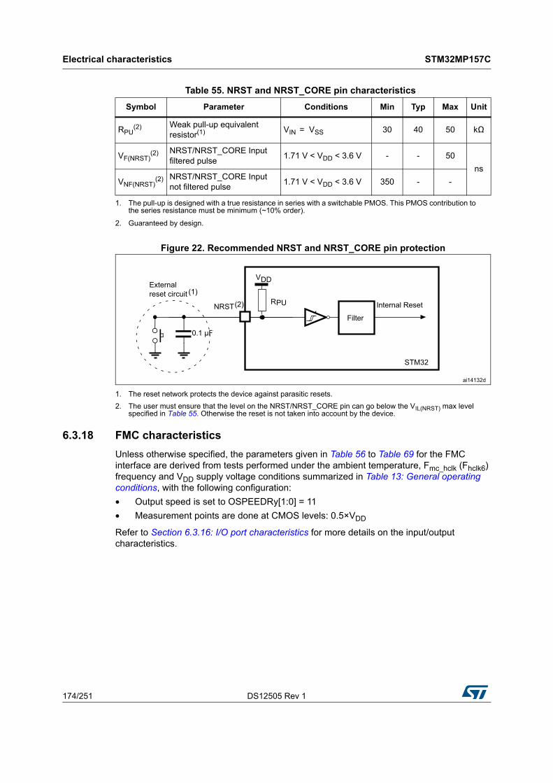
Electrical characteristics STM32MP157C
174/251 DS12505 Rev 1
Figure 22. Recommended NRST and NRST_CORE pin protection
1. The reset network protects the device against parasitic resets.
2. The user must ensure that the level on the NRST/NRST_CORE pin can go below the VIL(NRST) max level specified in Table 55. Otherwise the reset is not taken into account by the device.
6.3.18 FMC characteristics
Unless otherwise specified, the parameters given in Table 56 to Table 69 for the FMC interface are derived from tests performed under the ambient temperature, Fmc_hclk (Fhclk6) frequency and VDD supply voltage conditions summarized in Table 13: General operating conditions, with the following configuration:
• Output speed is set to OSPEEDRy[1:0] = 11
• Measurement points are done at CMOS levels: 0.5×VDD
Refer to Section 6.3.16: I/O port characteristics for more details on the input/output characteristics.
Table 55. NRST and NRST_CORE pin characteristics
Symbol Parameter Conditions Min Typ Max Unit
RPU(2) Weak pull-up equivalent
resistor(1)
1. The pull-up is designed with a true resistance in series with a switchable PMOS. This PMOS contribution to the series resistance must be minimum (~10% order).
VIN = VSS 30 40 50 kΩ
VF(NRST)(2)
2. Guaranteed by design.
NRST/NRST_CORE Input filtered pulse
1.71 V < VDD < 3.6 V - - 50
ns
VNF(NRST)(2) NRST/NRST_CORE Input
not filtered pulse1.71 V < VDD < 3.6 V 350 - -
ai14132d
STM32
RPUNRST(2)
VDD
Filter
Internal Reset
0.1 μF
Externalreset circuit (1)

DS12505 Rev 1 175/251
STM32MP157C Electrical characteristics
234
Asynchronous waveforms and timings
Figure 23 through Figure 26 represent asynchronous waveforms and Table 56 through Table 63 provide the corresponding timings. The results shown in these tables are obtained with the following FMC configuration:
• AddressSetupTime = 0x1
• AddressHoldTime = 0x1
• DataSetupTime = 0x1 (except for asynchronous NWAIT mode, DataSetupTime = 0x5)
• DataHoldTime = 0x1 (1×Tfmc_ker_ck for read operations and 2×Tfmc_ker_ck for write operations)
• ByteLaneSetup = 0x1
• BusTurnAroundDuration = 0x0
• Capacitive load CL = 30 pF
In all the timing tables, the Tfmc_ker_ck is the fmc_ker_ck clock period.
Figure 23. Asynchronous non-multiplexed SRAM/PSRAM/NOR read waveforms
1. Mode 2/B, C and D only. In Mode 1, FMC_NADV is not used.
Data
FMC_NE
FMC_NBL[1:0]
FMC_D[15:0]
tv(BL_NE)
t h(Data_NE)
FMC_NOE
AddressFMC_A[25:0]
tv(A_NE)
FMC_NWE
tsu(Data_NE)
tw(NE)
MS32753V1
w(NOE)ttv(NOE_NE) t h(NE_NOE)
th(Data_NOE)
t h(A_NOE)
t h(BL_NOE)
tsu(Data_NOE)
FMC_NADV (1)
t v(NADV_NE)
tw(NADV)
FMC_NWAIT
tsu(NWAIT_NE)
th(NE_NWAIT)

Electrical characteristics STM32MP157C
176/251 DS12505 Rev 1
Table 56. Asynchronous non-multiplexed SRAM/PSRAM/NOR read timings(1)
Symbol Parameter Min Max Unit
tw(NE) FMC_NE low time 3Tfmc_ker_ck-1 3Tfmc_ker_ck+0.5
ns
tv(NOE_NE) FMC_NEx low to FMC_NOE low 0 1
tw(NOE) FMC_NOE low time 2Tfmc_ker_ck-1 2Tfmc_ker_ck+1
th(NE_NOE) FMC_NOE high to FMC_NE high hold time Tfmc_ker_ck-1 -
tv(A_NE) FMC_NEx low to FMC_A valid - 1
th(A_NOE) Address hold time after FMC_NOE high 2Tfmc_ker_ck-1 -
tsu(Data_NE) Data to FMC_NEx high setup time Tfmc_ker_ck+15 -
tsu(Data_NOE) Data to FMC_NOEx high setup time 16 -
th(Data_NOE) Data hold time after FMC_NOE high 0 -
th(Data_NE) Data hold time after FMC_NEx high 0 -
tv(NADV_NE) FMC_NEx low to FMC_NADV low - 0
tw(NADV) FMC_NADV low time - Tfmc_ker_ck+1
1. Guaranteed by characterization results.
Table 57. Asynchronous non-multiplexed SRAM/PSRAM/NOR read - NWAIT timings(1)(2)
Symbol Parameter Min Max Unit
tw(NE) FMC_NE low time 7Tfmc_ker_ck-0.5 7Tfmc_ker_ck+1
ns
tw(NOE) FMC_NWE low time 6Tfmc_ker_ck-0.5 6Tfmc_ker_ck+1
tw(NWAIT) FMC_NWAIT low time Tfmc_ker_ck -
tsu(NWAIT_NE) FMC_NWAIT valid before FMC_NEx high 7Tfmc_ker_ck+2 -
th(NE_NWAIT) FMC_NEx hold time after FMC_NWAIT invalid 5Tfmc_ker_ck -
1. Guaranteed by characterization results.
2. NWAIT pulse width is equal to 1 AHB cycle.
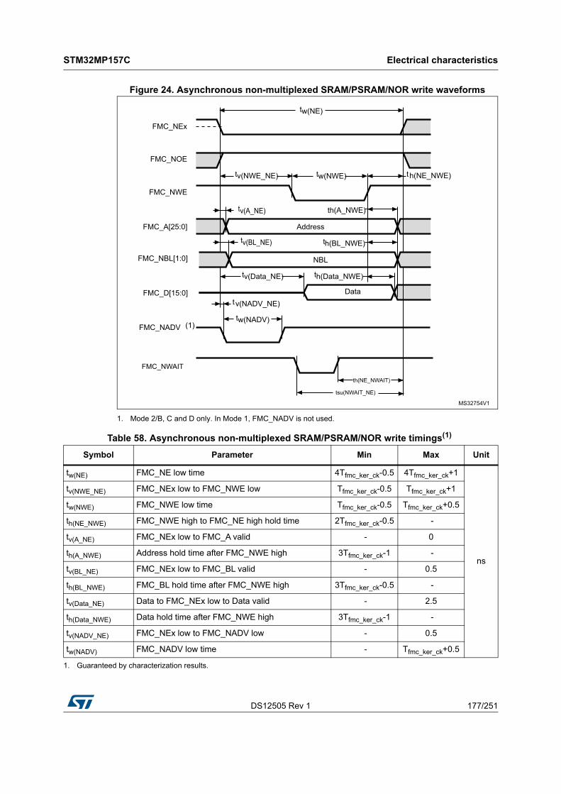
DS12505 Rev 1 177/251
STM32MP157C Electrical characteristics
234
Figure 24. Asynchronous non-multiplexed SRAM/PSRAM/NOR write waveforms
1. Mode 2/B, C and D only. In Mode 1, FMC_NADV is not used.
NBL
Data
FMC_NEx
FMC_NBL[1:0]
FMC_D[15:0]
tv(BL_NE)
th(Data_NWE)
FMC_NOE
AddressFMC_A[25:0]
tv(A_NE)
tw(NWE)
FMC_NWE
tv(NWE_NE) th(NE_NWE)
th(A_NWE)
th(BL_NWE)
tv(Data_NE)
tw(NE)
MS32754V1
FMC_NADV (1)
tv(NADV_NE)
tw(NADV)
FMC_NWAIT
tsu(NWAIT_NE)
th(NE_NWAIT)
Table 58. Asynchronous non-multiplexed SRAM/PSRAM/NOR write timings(1)
Symbol Parameter Min Max Unit
tw(NE) FMC_NE low time 4Tfmc_ker_ck-0.5 4Tfmc_ker_ck+1
ns
tv(NWE_NE) FMC_NEx low to FMC_NWE low Tfmc_ker_ck-0.5 Tfmc_ker_ck+1
tw(NWE) FMC_NWE low time Tfmc_ker_ck-0.5 Tfmc_ker_ck+0.5
th(NE_NWE) FMC_NWE high to FMC_NE high hold time 2Tfmc_ker_ck-0.5 -
tv(A_NE) FMC_NEx low to FMC_A valid - 0
th(A_NWE) Address hold time after FMC_NWE high 3Tfmc_ker_ck-1 -
tv(BL_NE) FMC_NEx low to FMC_BL valid - 0.5
th(BL_NWE) FMC_BL hold time after FMC_NWE high 3Tfmc_ker_ck-0.5 -
tv(Data_NE) Data to FMC_NEx low to Data valid - 2.5
th(Data_NWE) Data hold time after FMC_NWE high 3Tfmc_ker_ck-1 -
tv(NADV_NE) FMC_NEx low to FMC_NADV low - 0.5
tw(NADV) FMC_NADV low time - Tfmc_ker_ck+0.5
1. Guaranteed by characterization results.

Electrical characteristics STM32MP157C
178/251 DS12505 Rev 1
Figure 25. Asynchronous multiplexed PSRAM/NOR read waveforms
Table 59. Asynchronous non-multiplexed SRAM/PSRAM/NOR write - NWAIT timings(1)(2)
Symbol Parameter Min Max Unit
tw(NE) FMC_NE low time 8Tfmc_ker_ck-0.5 8Tfmc_ker_ck+0.5
nstw(NWE) FMC_NWE low time 5Tfmc_ker_ck-0.5 5Tfmc_ker_ck+1
tsu(NWAIT_NE) FMC_NWAIT valid before FMC_NEx high 8Tfmc_ker_ck+4 -
th(NE_NWAIT) FMC_NEx hold time after FMC_NWAIT invalid 6Tfmc_ker_ck -
1. Guaranteed by characterization results.
2. NWAIT pulse width is equal to 1 AHB cycle.
NBL
Data
FMC_ NBL[1:0]
FMC_ AD[15:0]
tv(BL_NE)
th(Data_NE)
AddressFMC_ A[25:16]
tv(A_NE)
FMC_NWE
tv(A_NE)
MS32755V1
Address
FMC_NADV
tv(NADV_NE)tw(NADV)
tsu(Data_NE)
th(AD_NADV)
FMC_ NE
FMC_NOE
tw(NE)
tw(NOE)
tv(NOE_NE) th(NE_NOE)
th(A_NOE)
th(BL_NOE)
tsu(Data_NOE) th(Data_NOE)
FMC_NWAIT
tsu(NWAIT_NE)
th(NE_NWAIT)
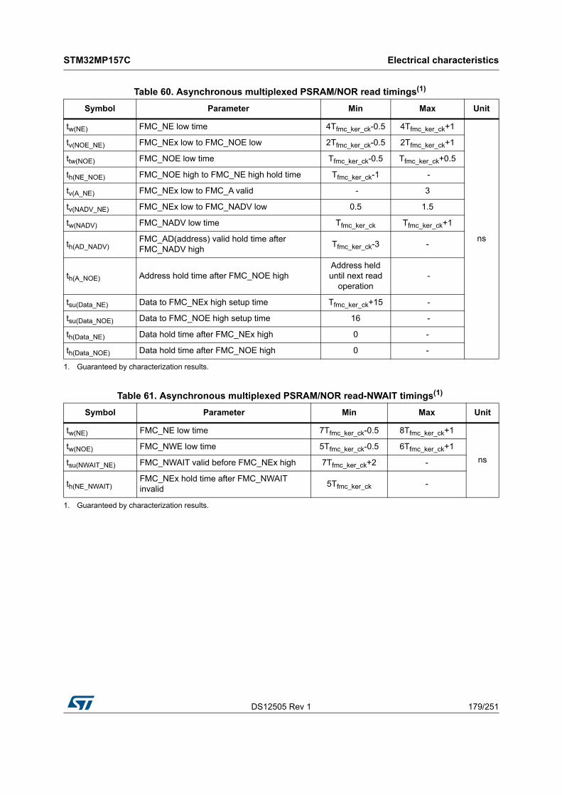
DS12505 Rev 1 179/251
STM32MP157C Electrical characteristics
234
Table 60. Asynchronous multiplexed PSRAM/NOR read timings(1)
Symbol Parameter Min Max Unit
tw(NE) FMC_NE low time 4Tfmc_ker_ck-0.5 4Tfmc_ker_ck+1
ns
tv(NOE_NE) FMC_NEx low to FMC_NOE low 2Tfmc_ker_ck-0.5 2Tfmc_ker_ck+1
ttw(NOE) FMC_NOE low time Tfmc_ker_ck-0.5 Tfmc_ker_ck+0.5
th(NE_NOE) FMC_NOE high to FMC_NE high hold time Tfmc_ker_ck-1 -
tv(A_NE) FMC_NEx low to FMC_A valid - 3
tv(NADV_NE) FMC_NEx low to FMC_NADV low 0.5 1.5
tw(NADV) FMC_NADV low time Tfmc_ker_ck Tfmc_ker_ck+1
th(AD_NADV)FMC_AD(address) valid hold time after FMC_NADV high
Tfmc_ker_ck-3 -
th(A_NOE) Address hold time after FMC_NOE highAddress held until next read
operation -
tsu(Data_NE) Data to FMC_NEx high setup time Tfmc_ker_ck+15 -
tsu(Data_NOE) Data to FMC_NOE high setup time 16 -
th(Data_NE) Data hold time after FMC_NEx high 0 -
th(Data_NOE) Data hold time after FMC_NOE high 0 -
1. Guaranteed by characterization results.
Table 61. Asynchronous multiplexed PSRAM/NOR read-NWAIT timings(1)
Symbol Parameter Min Max Unit
tw(NE) FMC_NE low time 7Tfmc_ker_ck-0.5 8Tfmc_ker_ck+1
ns
tw(NOE) FMC_NWE low time 5Tfmc_ker_ck-0.5 6Tfmc_ker_ck+1
tsu(NWAIT_NE) FMC_NWAIT valid before FMC_NEx high 7Tfmc_ker_ck+2 -
th(NE_NWAIT)FMC_NEx hold time after FMC_NWAIT invalid
5Tfmc_ker_ck -
1. Guaranteed by characterization results.
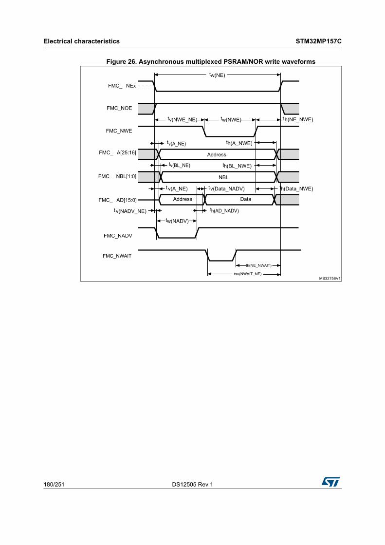
Electrical characteristics STM32MP157C
180/251 DS12505 Rev 1
Figure 26. Asynchronous multiplexed PSRAM/NOR write waveforms
NBL
Data
FMC_ NEx
FMC_ NBL[1:0]
FMC_ AD[15:0]
tv(BL_NE)
th(Data_NWE)
FMC_NOE
AddressFMC_ A[25:16]
tv(A_NE)
tw(NWE)
FMC_NWE
tv(NWE_NE) th(NE_NWE)
th(A_NWE)
th(BL_NWE)
tv(A_NE)
tw(NE)
MS32756V1
Address
FMC_NADV
tv(NADV_NE)
tw(NADV)
tv(Data_NADV)
th(AD_NADV)
FMC_NWAIT
tsu(NWAIT_NE)
th(NE_NWAIT)
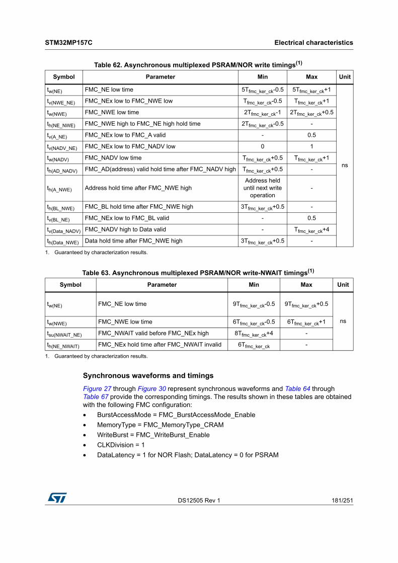
DS12505 Rev 1 181/251
STM32MP157C Electrical characteristics
234
Synchronous waveforms and timings
Figure 27 through Figure 30 represent synchronous waveforms and Table 64 through Table 67 provide the corresponding timings. The results shown in these tables are obtained with the following FMC configuration:
• BurstAccessMode = FMC_BurstAccessMode_Enable
• MemoryType = FMC_MemoryType_CRAM
• WriteBurst = FMC_WriteBurst_Enable
• CLKDivision = 1
• DataLatency = 1 for NOR Flash; DataLatency = 0 for PSRAM
Table 62. Asynchronous multiplexed PSRAM/NOR write timings(1)
Symbol Parameter Min Max Unit
tw(NE) FMC_NE low time 5Tfmc_ker_ck-0.5 5Tfmc_ker_ck+1
ns
tv(NWE_NE) FMC_NEx low to FMC_NWE low Tfmc_ker_ck-0.5 Tfmc_ker_ck+1
tw(NWE) FMC_NWE low time 2Tfmc_ker_ck-1 2Tfmc_ker_ck+0.5
th(NE_NWE) FMC_NWE high to FMC_NE high hold time 2Tfmc_ker_ck-0.5 -
tv(A_NE) FMC_NEx low to FMC_A valid - 0.5
tv(NADV_NE) FMC_NEx low to FMC_NADV low 0 1
tw(NADV) FMC_NADV low time Tfmc_ker_ck+0.5 Tfmc_ker_ck+1
th(AD_NADV) FMC_AD(address) valid hold time after FMC_NADV high Tfmc_ker_ck+0.5 -
th(A_NWE) Address hold time after FMC_NWE highAddress held
until next write operation
-
th(BL_NWE) FMC_BL hold time after FMC_NWE high 3Tfmc_ker_ck+0.5 -
tv(BL_NE) FMC_NEx low to FMC_BL valid - 0.5
tv(Data_NADV) FMC_NADV high to Data valid - Tfmc_ker_ck+4
th(Data_NWE) Data hold time after FMC_NWE high 3Tfmc_ker_ck+0.5 -
1. Guaranteed by characterization results.
Table 63. Asynchronous multiplexed PSRAM/NOR write-NWAIT timings(1)
Symbol Parameter Min Max Unit
tw(NE) FMC_NE low time 9Tfmc_ker_ck-0.5 9Tfmc_ker_ck+0.5
nstw(NWE) FMC_NWE low time 6Tfmc_ker_ck-0.5 6Tfmc_ker_ck+1
tsu(NWAIT_NE) FMC_NWAIT valid before FMC_NEx high 8Tfmc_ker_ck+4 -
th(NE_NWAIT) FMC_NEx hold time after FMC_NWAIT invalid 6Tfmc_ker_ck -
1. Guaranteed by characterization results.

Electrical characteristics STM32MP157C
182/251 DS12505 Rev 1
In all the timing tables, the Tfmc_ker_ck is the fmc_ker_ck clock period, with the following FMC_CLK maximum values:
• For 2.7 V < VDD < 3.6 V, FMC_CLK = 130 MHz at 20 pF
• For 1.71 V < VDD < 1.9 V, FMC_CLK = 95 MHz at 20 pF
Figure 27. Synchronous multiplexed NOR/PSRAM read timings
FMC_CLK
FMC_NEx
FMC_NADV
FMC_A[25:16]
FMC_NOE
FMC_AD[15:0] AD[15:0] D1 D2
FMC_NWAIT(WAITCFG = 1b, WAITPOL + 0b)
FMC_NWAIT(WAITCFG = 0b, WAITPOL + 0b)
tw(CLK) tw(CLK)
Data latency = 0
BUSTURN = 0
td(CLKL-NExL) td(CLKH-NExH)
td(CLKL-NADVL)
td(CLKL-AV)
td(CLKL-NADVH)
td(CLKH-AIV)
td(CLKL-NOEL) td(CLKH-NOEH)
td(CLKL-ADV)
td(CLKL-ADIV)tsu(ADV-CLKH)
th(CLKH-ADV)tsu(ADV-CLKH) th(CLKH-ADV)
tsu(NWAITV-CLKH) th(CLKH-NWAITV)
tsu(NWAITV-CLKH) th(CLKH-NWAITV)
tsu(NWAITV-CLKH) th(CLKH-NWAITV)
MS32757V1
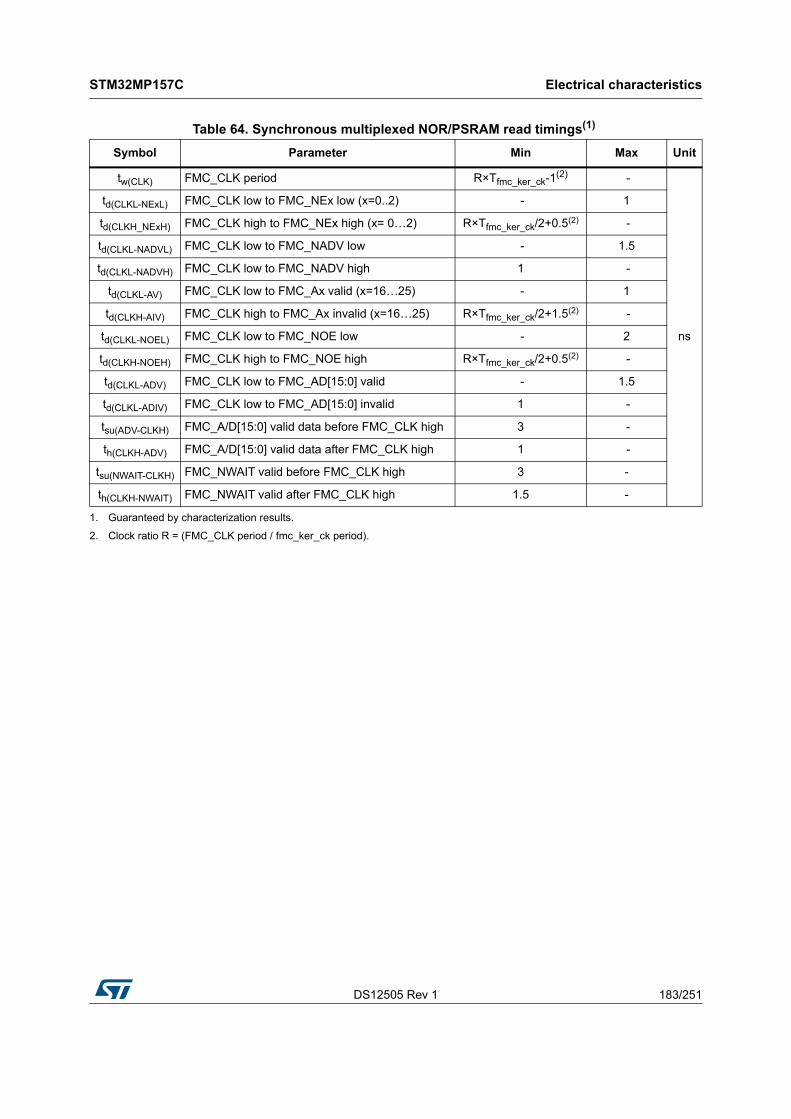
DS12505 Rev 1 183/251
STM32MP157C Electrical characteristics
234
Table 64. Synchronous multiplexed NOR/PSRAM read timings(1)
Symbol Parameter Min Max Unit
tw(CLK) FMC_CLK period R×Tfmc_ker_ck-1(2) -
ns
td(CLKL-NExL) FMC_CLK low to FMC_NEx low (x=0..2) - 1
td(CLKH_NExH) FMC_CLK high to FMC_NEx high (x= 0…2) R×Tfmc_ker_ck/2+0.5(2) -
td(CLKL-NADVL) FMC_CLK low to FMC_NADV low - 1.5
td(CLKL-NADVH) FMC_CLK low to FMC_NADV high 1 -
td(CLKL-AV) FMC_CLK low to FMC_Ax valid (x=16…25) - 1
td(CLKH-AIV) FMC_CLK high to FMC_Ax invalid (x=16…25) R×Tfmc_ker_ck/2+1.5(2) -
td(CLKL-NOEL) FMC_CLK low to FMC_NOE low - 2
td(CLKH-NOEH) FMC_CLK high to FMC_NOE high R×Tfmc_ker_ck/2+0.5(2) -
td(CLKL-ADV) FMC_CLK low to FMC_AD[15:0] valid - 1.5
td(CLKL-ADIV) FMC_CLK low to FMC_AD[15:0] invalid 1 -
tsu(ADV-CLKH) FMC_A/D[15:0] valid data before FMC_CLK high 3 -
th(CLKH-ADV) FMC_A/D[15:0] valid data after FMC_CLK high 1 -
tsu(NWAIT-CLKH) FMC_NWAIT valid before FMC_CLK high 3 -
th(CLKH-NWAIT) FMC_NWAIT valid after FMC_CLK high 1.5 -
1. Guaranteed by characterization results.
2. Clock ratio R = (FMC_CLK period / fmc_ker_ck period).

Electrical characteristics STM32MP157C
184/251 DS12505 Rev 1
Figure 28. Synchronous multiplexed PSRAM write timings
FMC_CLK
FMC_NEx
FMC_NADV
FMC_A[25:16]
FMC_NWE
FMC_AD[15:0] AD[15:0] D1 D2
FMC_NWAIT(WAITCFG = 0b, WAITPOL + 0b)
tw(CLK) tw(CLK)
Data latency = 0
BUSTURN = 0
td(CLKL-NExL) td(CLKH-NExH)
td(CLKL-NADVL)
td(CLKL-AV)
td(CLKL-NADVH)
td(CLKH-AIV)
td(CLKH-NWEH)td(CLKL-NWEL)
td(CLKH-NBLH)
td(CLKL-ADV)
td(CLKL-ADIV) td(CLKL-Data)
tsu(NWAITV-CLKH) th(CLKH-NWAITV)
MS32758V1
td(CLKL-Data)
FMC_NBL
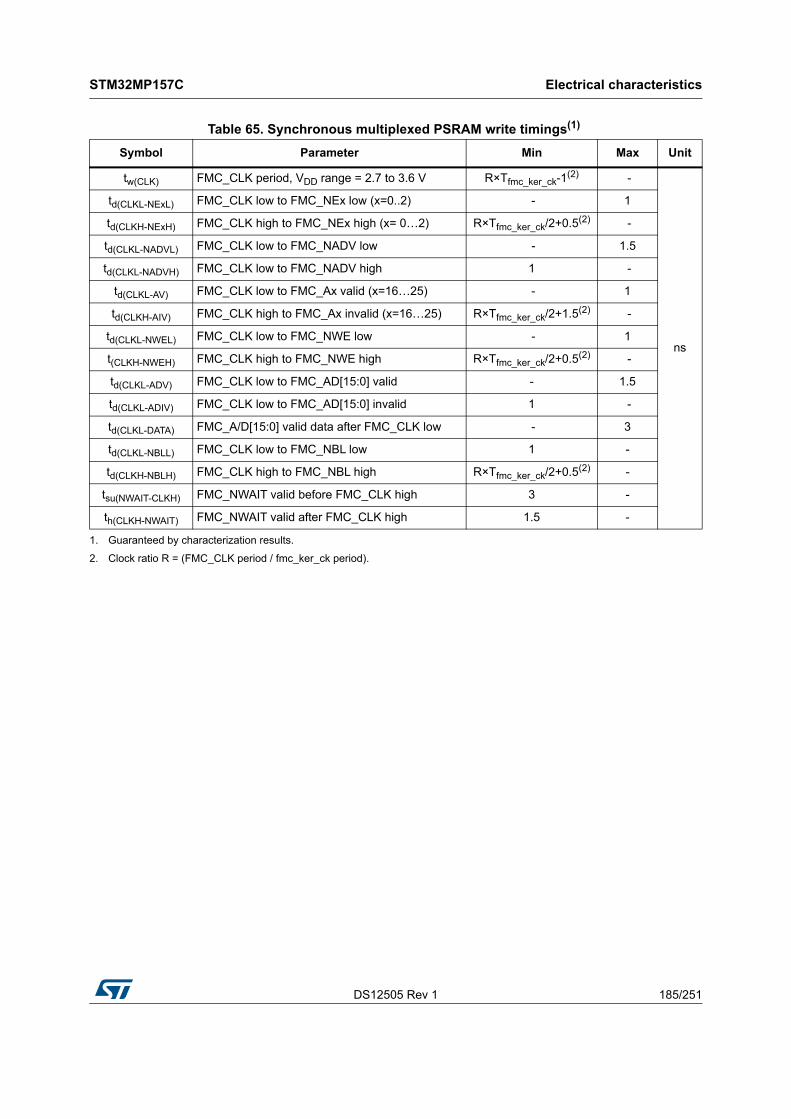
DS12505 Rev 1 185/251
STM32MP157C Electrical characteristics
234
Table 65. Synchronous multiplexed PSRAM write timings(1)
Symbol Parameter Min Max Unit
tw(CLK) FMC_CLK period, VDD range = 2.7 to 3.6 V R×Tfmc_ker_ck-1(2) -
ns
td(CLKL-NExL) FMC_CLK low to FMC_NEx low (x=0..2) - 1
td(CLKH-NExH) FMC_CLK high to FMC_NEx high (x= 0…2) R×Tfmc_ker_ck/2+0.5(2) -
td(CLKL-NADVL) FMC_CLK low to FMC_NADV low - 1.5
td(CLKL-NADVH) FMC_CLK low to FMC_NADV high 1 -
td(CLKL-AV) FMC_CLK low to FMC_Ax valid (x=16…25) - 1
td(CLKH-AIV) FMC_CLK high to FMC_Ax invalid (x=16…25) R×Tfmc_ker_ck/2+1.5(2) -
td(CLKL-NWEL) FMC_CLK low to FMC_NWE low - 1
t(CLKH-NWEH) FMC_CLK high to FMC_NWE high R×Tfmc_ker_ck/2+0.5(2) -
td(CLKL-ADV) FMC_CLK low to FMC_AD[15:0] valid - 1.5
td(CLKL-ADIV) FMC_CLK low to FMC_AD[15:0] invalid 1 -
td(CLKL-DATA) FMC_A/D[15:0] valid data after FMC_CLK low - 3
td(CLKL-NBLL) FMC_CLK low to FMC_NBL low 1 -
td(CLKH-NBLH) FMC_CLK high to FMC_NBL high R×Tfmc_ker_ck/2+0.5(2) -
tsu(NWAIT-CLKH) FMC_NWAIT valid before FMC_CLK high 3 -
th(CLKH-NWAIT) FMC_NWAIT valid after FMC_CLK high 1.5 -
1. Guaranteed by characterization results.
2. Clock ratio R = (FMC_CLK period / fmc_ker_ck period).

Electrical characteristics STM32MP157C
186/251 DS12505 Rev 1
Figure 29. Synchronous non-multiplexed NOR/PSRAM read timings
FMC_CLK
FMC_NEx
FMC_A[25:0]
FMC_NOE
FMC_D[15:0] D1 D2
FMC_NWAIT(WAITCFG = 1b, WAITPOL + 0b)
FMC_NWAIT(WAITCFG = 0b, WAITPOL + 0b)
tw(CLK) tw(CLK)
Data latency = 0td(CLKL-NExL) td(CLKH-NExH)
td(CLKL-AV) td(CLKH-AIV)
td(CLKL-NOEL) td(CLKH-NOEH)
tsu(DV-CLKH) th(CLKH-DV)tsu(DV-CLKH) th(CLKH-DV)
tsu(NWAITV-CLKH) th(CLKH-NWAITV)
tsu(NWAITV-CLKH) t h(CLKH-NWAITV)
tsu(NWAITV-CLKH) th(CLKH-NWAITV)
MS32759V1
FMC_NADV
td(CLKL-NADVL) td(CLKL-NADVH)
Table 66. Synchronous non-multiplexed NOR/PSRAM read timings(1)
Symbol Parameter Min Max Unit
tw(CLK) FMC_CLK period R×Tfmc_ker_ck-1(2) -
ns
t(CLKL-NExL) FMC_CLK low to FMC_NEx low (x=0..2) - 1
td(CLKH-NExH) FMC_CLK high to FMC_NEx high (x= 0…2) R×Tfmc_ker_ck/2+0.5(2) -
td(CLKL-NADVL) FMC_CLK low to FMC_NADV low - 1.5
td(CLKL-NADVH) FMC_CLK low to FMC_NADV high 1 -
td(CLKL-AV) FMC_CLK low to FMC_Ax valid (x=16…25) - 1
td(CLKH-AIV) FMC_CLK high to FMC_Ax invalid (x=16…25) R×Tfmc_ker_ck/2+1.5(2) -
td(CLKL-NOEL) FMC_CLK low to FMC_NOE low - 2
td(CLKH-NOEH) FMC_CLK high to FMC_NOE high R×Tfmc_ker_ck/2+1.5(2) -
tsu(DV-CLKH) FMC_D[15:0] valid data before FMC_CLK high 3 -
th(CLKH-DV) FMC_D[15:0] valid data after FMC_CLK high 1 -
t(NWAIT-CLKH) FMC_NWAIT valid before FMC_CLK high 3 -
th(CLKH-NWAIT) FMC_NWAIT valid after FMC_CLK high 1.5 -
1. Guaranteed by characterization results.

DS12505 Rev 1 187/251
STM32MP157C Electrical characteristics
234
Figure 30. Synchronous non-multiplexed PSRAM write timings
2. Clock ratio R = (FMC_CLK period / fmc_ker_ck period).
MS32760V1
FMC_CLK
FMC_NEx
FMC_A[25:0]
FMC_NWE
FMC_D[15:0] D1 D2
FMC_NWAIT(WAITCFG = 0b, WAITPOL + 0b)
tw(CLK) tw(CLK)
Data latency = 0td(CLKL-NExL) td(CLKH-NExH)
td(CLKL-AV)td(CLKH-AIV)
td(CLKH-NWEH)td(CLKL-NWEL)
td(CLKL-Data)
tsu(NWAITV-CLKH)
th(CLKH-NWAITV)
FMC_NADV
td(CLKL-NADVL) td(CLKL-NADVH)
td(CLKL-Data)
FMC_NBL
td(CLKH-NBLH)

Electrical characteristics STM32MP157C
188/251 DS12505 Rev 1
NAND controller waveforms and timings
Figure 31 through Figure 34 represent synchronous waveforms, and Table 68 and Table 69 provide the corresponding timings. The results shown in this table are obtained with the following FMC configuration:
• FMC_SetupTime = 0x01
• FMC_WaitSetupTime = 0x03
• FMC_HoldSetupTime = 0x02
• FMC_HiZSetupTime = 0x01
• Bank = FMC_Bank_NAND
• MemoryDataWidth = FMC_MemoryDataWidth_16b
• ECC = FMC_ECC_Enable
• ECCPageSize = FMC_ECCPageSize_512Bytes
• TCLRSetupTime = 0
• TARSetupTime = 0
• CL = 30 pF
In all timing tables, the Tfmc_ker_ck is the fmc_ker_ck clock period.
Table 67. Synchronous non-multiplexed PSRAM write timings(1)
Symbol Parameter Min Max Unit
t(CLK) FMC_CLK period R×Tfmc_ker_ck -1(2) -
ns
td(CLKL-NExL) FMC_CLK low to FMC_NEx low (x=0..2) - 1
t(CLKH-NExH) FMC_CLK high to FMC_NEx high (x= 0…2) R×Tfmc_ker_ck/2+0.5(2) -
td(CLKL-NADVL) FMC_CLK low to FMC_NADV low - 1.5
td(CLKL-NADVH) FMC_CLK low to FMC_NADV high 1 -
td(CLKL-AV) FMC_CLK low to FMC_Ax valid (x=16…25) - 1
td(CLKH-AIV) FMC_CLK high to FMC_Ax invalid (x=16…25) R×Tfmc_ker_ck/2+1.5(2) -
td(CLKL-NWEL) FMC_CLK low to FMC_NWE low - 1
td(CLKH-NWEH) FMC_CLK high to FMC_NWE high R×Tfmc_ker_ck/2+0.5(2) -
td(CLKL-Data) FMC_D[15:0] valid data after FMC_CLK low - 3
td(CLKL-NBLL) FMC_CLK low to FMC_NBL low 1 -
td(CLKH-NBLH) FMC_CLK high to FMC_NBL high R×Tfmc_ker_ck/2+0.5(2) -
tsu(NWAIT-CLKH) FMC_NWAIT valid before FMC_CLK high 3 -
th(CLKH-NWAIT) FMC_NWAIT valid after FMC_CLK high 1.5 -
1. Guaranteed by characterization results.
2. Clock ratio R = (FMC_CLK period / fmc_ker_ck period).

DS12505 Rev 1 189/251
STM32MP157C Electrical characteristics
234
Figure 31. NAND controller waveforms for read access
Figure 32. NAND controller waveforms for write access
FMC_NWE
FMC_NOE (NRE)
FMC_D[15:0]
tsu(D-NOE) th(NOE-D)
MS32767V1
ALE (FMC_A17)CLE (FMC_A16)
FMC_NCEx
td(ALE-NOE) th(NOE-ALE)
MS32768V1
th(NWE-D)tv(NWE-D)
FMC_NWE
FMC_NOE (NRE)
FMC_D[15:0]
ALE (FMC_A17)CLE (FMC_A16)
FMC_NCEx
td(ALE-NWE) th(NWE-ALE)

Electrical characteristics STM32MP157C
190/251 DS12505 Rev 1
Figure 33. NAND controller waveforms for common memory read access
Figure 34. NAND controller waveforms for common memory write access
MS32769V1
FMC_NWE
FMC_NOE
FMC_D[15:0]
tw(NOE)
tsu(D-NOE) th(NOE-D)
ALE (FMC_A17)CLE (FMC_A16)
FMC_NCEx
td(ALE-NOE) th(NOE-ALE)
MS32770V1
tw(NWE)
th(NWE-D)tv(NWE-D)
FMC_NWE
FMC_N OE
FMC_D[15:0]
td(D-NWE)
ALE (FMC_A17)CLE (FMC_A16)
FMC_NCEx
td(ALE-NOE) th(NOE-ALE)
Table 68. Switching characteristics for NAND Flash read cycles(1)
Symbol Parameter Min Max Unit
tw(N0E) FMC_NOE low width 4Tfmc_ker_ck-1 4Tfmc_ker_ck+1
ns
tsu(D-NOE) FMC_D[15-0] valid data before FMC_NOE high 11 -
th(NOE-D) FMC_D[15-0] valid data after FMC_NOE high 0 -
td(ALE-NOE) FMC_ALE valid before FMC_NOE low - 2Tfmc_ker_ck+1
th(NOE-ALE) FMC_NWE high to FMC_ALE invalid 3Tfmc_ker_ck+0.5 -
1. Guaranteed by characterization results.

DS12505 Rev 1 191/251
STM32MP157C Electrical characteristics
234
6.3.19 QUADSPI interface characteristics
Unless otherwise specified, the parameters given in Table 70 and Table 71 for QUADSPI are derived from tests performed under the ambient temperature, Faxiss_ck frequency and VDD supply voltage conditions summarized in Table 13: General operating conditions, with the following configuration:
• Output speed is set to OSPEEDRy[1:0] = 11
• Measurement points are done at CMOS levels: 0.5×VDD
• I/O compensation cell enabled
• HSLV activated when VDD ≤ 2.7 V
Refer to Section 0.3.16: I/O port characteristics for more details on the input/output alternate function characteristics.
Table 69. Switching characteristics for NAND Flash write cycles(1)
Symbol Parameter Min Max Unit
tw(NWE) FMC_NWE low width 4Tfmc_ker_ck-1 4Tfmc_ker_ck+1
ns
tv(NWE-D) FMC_NWE low to FMC_D[15-0] valid 0 -
th(NWE-D) FMC_NWE high to FMC_D[15-0] invalid 3Tfmc_ker_ck -
td(D-NWE) FMC_D[15-0] valid before FMC_NWE high 4Tfmc_ker_ck-3 -
td(ALE-NWE) FMC_ALE valid before FMC_NWE low - 2Tfmc_ker_ck+1
th(NWE-ALE) FMC_NWE high to FMC_ALE invalid 3Tfmc_ker_ck+0.5 -
1. Guaranteed by characterization results.
Table 70. QUADSPI characteristics in SDR mode
Symbol Parameter Conditions Min Typ Max Unit
Fck1/t(CLK) QUADSPI clock frequency
2.7 V ≤ VDD < 3.6 V
CL = 20 pF- - 166
MHz1.71 V < VDD <3.6 V
CL = 15 pF - - 90
tw(CLKH) QUADSPI clock high and low time
-t(CLK)/2 - 0.5 - t(CLK)/2 + 0.5
ns
tw(CLKL) t(CLK)/2 - 0.5 - t(CLK)/2 + 0.5
ts(IN) Data input setup time - 1.25 - -
th(IN) Data input hold time - 2.75 - -
tv(OUT) Data output valid time - - 1 1.5
th(OUT) Data output hold time - 0 - -
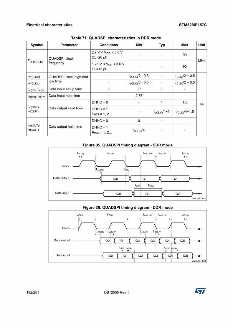
Electrical characteristics STM32MP157C
192/251 DS12505 Rev 1
Figure 35. QUADSPI timing diagram - SDR mode
Figure 36. QUADSPI timing diagram - DDR mode
Table 71. QUADSPI characteristics in DDR mode
Symbol Parameter Conditions Min Typ Max Unit
Fck1/t(CLK)QUADSPI clock frequency
2.7 V < VDD < 3.6 V
CL=20 pF- - 90
MHz1.71 V < VDD < 3.6 V
CL=15 pF- - 90
tw(CLKH) QUADSPI clock high and low time
- t(CLK)/2 - 0.5 - t(CLK)/2 + 0.5
ns
tw(CLKL) - t(CLK)/2 - 0.5 - t(CLK)/2 + 0.5
tsr(IN), tsf(IN) Data input setup time - 0.5 - -
thr(IN), thf(IN) Data input hold time - 2.75 - -
tvr(OUT), tvf(OUT)
Data output valid time
DHHC = 0 - 1 1.5
DHHC = 1
Pres = 1, 2...- t(CLK)/4+1 t(CLK)/4+1.5
thr(OUT), thf(OUT)
Data output hold time
DHHC = 0 0 - -
DHHC = 1
Pres = 1, 2...t(CLK)/4 - -
MSv36878V2
Data output IO0 IO1 IO2
Clock
Data input IO0 IO1 IO2
t(CLK) tw(CLKH) tw(CLKL)tr(CLK) tf(CLK)
ts(IN) th(IN)
tv(OUT) th(OUT)
MSv36879V2
Data output IO0 IO2 IO4
Clock
Data input IO0 IO2 IO4
t(CLK) tw(CLKH) tw(CLKL)tr(CLK) tf(CLK)
tsf(IN) thf(IN)
tvf(OUT) thr(OUT)
IO1 IO3 IO5
IO1 IO3 IO5
tvr(OUT) thf(OUT)
tsr(IN) thr(IN)
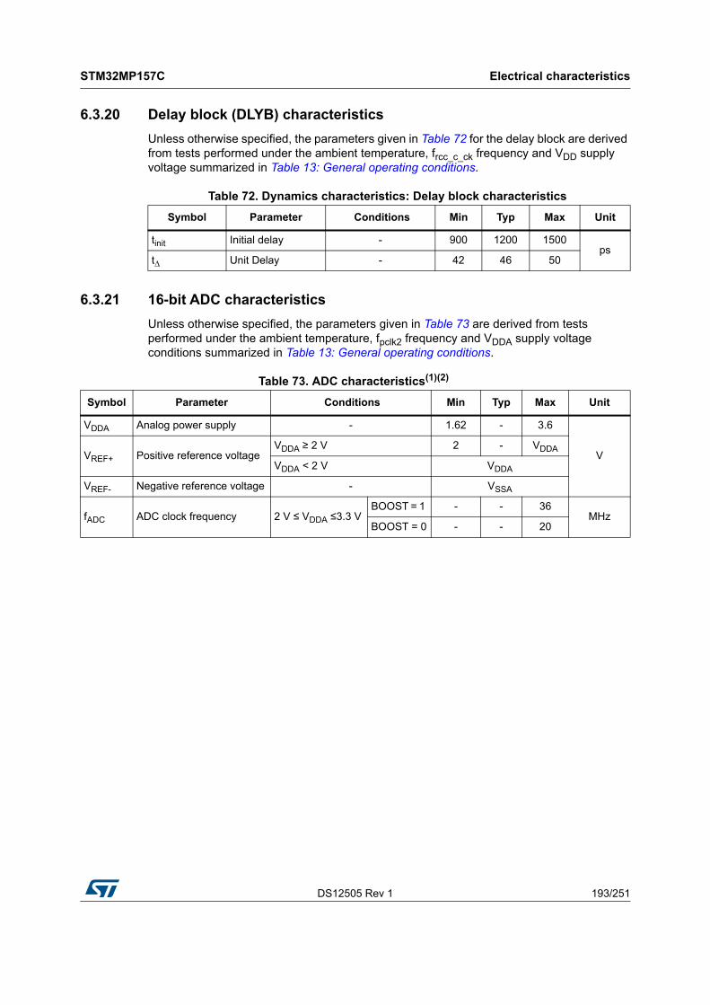
DS12505 Rev 1 193/251
STM32MP157C Electrical characteristics
234
6.3.20 Delay block (DLYB) characteristics
Unless otherwise specified, the parameters given in Table 72 for the delay block are derived from tests performed under the ambient temperature, frcc_c_ck frequency and VDD supply voltage summarized in Table 13: General operating conditions.
6.3.21 16-bit ADC characteristics
Unless otherwise specified, the parameters given in Table 73 are derived from tests performed under the ambient temperature, fpclk2 frequency and VDDA supply voltage conditions summarized in Table 13: General operating conditions.
Table 72. Dynamics characteristics: Delay block characteristics
Symbol Parameter Conditions Min Typ Max Unit
tinit Initial delay - 900 1200 1500ps
t∆ Unit Delay - 42 46 50
Table 73. ADC characteristics(1)(2)
Symbol Parameter Conditions Min Typ Max Unit
VDDA Analog power supply - 1.62 - 3.6
VVREF+ Positive reference voltageVDDA ≥ 2 V 2 - VDDA
VDDA < 2 V VDDA
VREF- Negative reference voltage - VSSA
fADC ADC clock frequency 2 V ≤ VDDA ≤3.3 VBOOST = 1 - - 36
MHzBOOST = 0 - - 20

Electrical characteristics STM32MP157C
194/251 DS12505 Rev 1
fS
Sampling rate for Fast channels, BOOST = 1, fADC = 36 MHz, sampling time = 1.5 cycles
16-bit resolution - - 3.60
MSPS
14-bit resolution - - 4.00
12-bit resolution - - 4.50
10-bit resolution - - 5.00
8-bit resolution - - 6.00
Sampling rate for Fast channels, BOOST = 0, fADC = 20 MHz, sampling time = 1.5 cycles
16-bit resolution - - 2.00
14-bit resolution - - 2.20
12-bit resolution - - 2.50
10-bit resolution - - 2.80
8-bit resolution - - 3.30
Sampling rate for Slow channels, BOOST = 1, fADC = 28 MHz, sampling time = 2.5 cycles
16-bit resolution - - 2.55
14-bit resolution - - 2.80
12-bit resolution - - 3.11
10-bit resolution - - 3.50
8-bit resolution - - 4.00
Sampling rate for Slow channels, BOOST = 0, fADC = 20 MHz, sampling time = 2.5 cycles
16-bit resolution - - 1.82
14-bit resolution - - 2.00
12-bit resolution - - 2.22
10-bit resolution - - 2.50
8-bit resolution - - 2.86
fTRIG External trigger frequencyfADC = 36 MHz - - 3.6 MHz
16-bit resolution - - 10 1/fADC
VAIN(3) Conversion voltage range - 0 - VREF+
VVCMIV
Common mode input voltage
-VREF/2-
10%VREF/2
VREF/2+10%
CADCInternal sample and hold capacitor
- - 4 - pF
tADCREG_
STUPADC LDO startup time - - 5 10 µs
tSTAB ADC power-up time LDO already started 1 1/fADC
Table 73. ADC characteristics(1)(2) (continued)
Symbol Parameter Conditions Min Typ Max Unit

DS12505 Rev 1 195/251
STM32MP157C Electrical characteristics
234
tCALOffset and linearity calibration time
- 16384
1/fADC
tOFF_CAL Offset calibration time - 1280
tLATR
Trigger conversion latency for regular and injected channels without aborting the conversion
CKMODE = 00 1.5 2 2.5
CKMODE = 01 - - 2.5
CKMODE = 10 - - 2.5
CKMODE = 11 - - 2.25
tLATRINJ
Trigger conversion latency for regular and injected channels when a regular conversion is aborted
CKMODE = 00 2.5 3 3.5
CKMODE = 01 - - 3.5
CKMODE = 10 - - 3.5
CKMODE = 11 - - 3.25
tS Sampling time - 1.5 - 810.5
tCONVTotal conversion time (including sampling time)
N-bit resolution ts + N/2(4)
IDDA(ADC)ADC consumption from VDDA supply (differential)
FS = 3.6 Msps, BOOST = 1 - 1900 -
μA
FS = 1 Msps, BOOST = 0 - 460 -
IDDA(REF)ADC consumption from VREF+ (differential)
FS = 3.6 Msps, BOOST = 1 - 260 -
FS = 1 Msps, BOOST = 0 - 140 -
IDDA(ADC)ADC consumption from VDDA supply (single-ended)
FS = 3.6 Msps, BOOST = 1 - 1700 -
FS = 1 Msps, BOOST = 0 - 445 -
IDDA(REF)
ADC consumption from VREF+ supply (single-ended)
FS = 3.6 Msps, BOOST = 1 - 160 -
FS = 1 Msps, BOOST = 0 - 75 -
IDD(ADC)ADC consumption from VDD supply
FS = 3.6 Msps - 250 -
FS = 1 Msps - 50 -
1. Guaranteed by design.
2. Voltage BOOSTER on ADC switches must be used for VDDA < 2.4 V (switches inside IO).
3. Depending on the package, VREF- can be internally connected to VSSA.
4. 9 to 818 cycles @ 14-bit mode.
Table 73. ADC characteristics(1)(2) (continued)
Symbol Parameter Conditions Min Typ Max Unit

Electrical characteristics STM32MP157C
196/251 DS12505 Rev 1
Table 74. Minimum sampling time versus RAIN with 47 pF PCB capacitorup to 125 °C and VDDA = 1.6 V(1)
Resolution(2) RAIN (Ω)Fast
channels(3)Slow
channels(4)
16 bits 47(5) 1.07E-07 1.66E-07
14 bits
47 9.08E-08 1.44E-07
68 9.67E-07 1.51E-07
100 1.08E-07 1.57E-07
150 1.28E-07 1.71E-07
220(5) 1.61E-07 1.92E-07
12 bits
47 7.67E-08 1.25E-07
68 8.15E-08 1.27E-07
100 8.98E-08 1.34E-07
150 1.07E-07 1.46E-07
220 1.32E-07 1.69E-07
330 1.77E-07 2.05E-07
470 2.36E-07 2.64E-07
680 3.29E-07 3.45E-07
1000(5) 4.62E-07 4.88E-07
10 bits
47 6.25E-08 1.03E-07
68 6.62E-08 1.06E-07
100 7.27E-08 1.12E-07
150 8.54E-08 1.21E-07
220 1.06E-07 1.37E-07
330 1.40E-07 1.68E-07
470 1.87E-07 2.09E-07
680 2.58E-07 2.79E-07
1000 3.67E-07 3.81E-07
1500 5.37E-07 5.52E-07
2200 7.76E-07 7.86E-07
3300 1.13E-06 1.14E-06
4700(5) 1.60E-06 1.60E-06

DS12505 Rev 1 197/251
STM32MP157C Electrical characteristics
234
8 bits
47 4.87E-08 8.24E-08
68 5.14E-08 8.46E-08
100 5.64E-08 8.87E-08
150 6.58E-08 9.57E-08
220 8.04E-08 1.08E-07
330 1.06E-07 1.30E-07
470 1.39E-07 1.60E-07
680 1.89E-07 2.08E-07
1000 2.69E-07 2.84E-07
1500 3.90E-07 4.05E-07
2200 5.62E-07 5.72E-07
3300 8.27E-07 8.40E-07
4700 1.17E-06 1.17E-06
6800 1.67E-06 1.67E-06
10000 2.44E-06 2.43E-06
15000 3.66E-06 3.63E-06
2200(5) 5.36E-06 5.31E-06
1. Guaranteed by design.
2. The tolerance is 8 LSB for 16-bit, 4 LSB for 14-bit, 2 LSB for 12-bit, 10-bit and 8-bit conversions.
3. On ADC1, fast channels are PA6, PA7, PB0, PB1, PC4, PC5, PF11, PF12. On ADC2, fast channels are PA6, PA7, PB0, PB1, PC4, PC5, PF13, PF14.
4. Slow channels are all ADC inputs except the fast channels.
5. Maximum external input impedance value authorized for the given resolution.
Table 74. Minimum sampling time versus RAIN with 47 pF PCB capacitorup to 125 °C and VDDA = 1.6 V(1) (continued)
Resolution(2) RAIN (Ω)Fast
channels(3)Slow
channels(4)
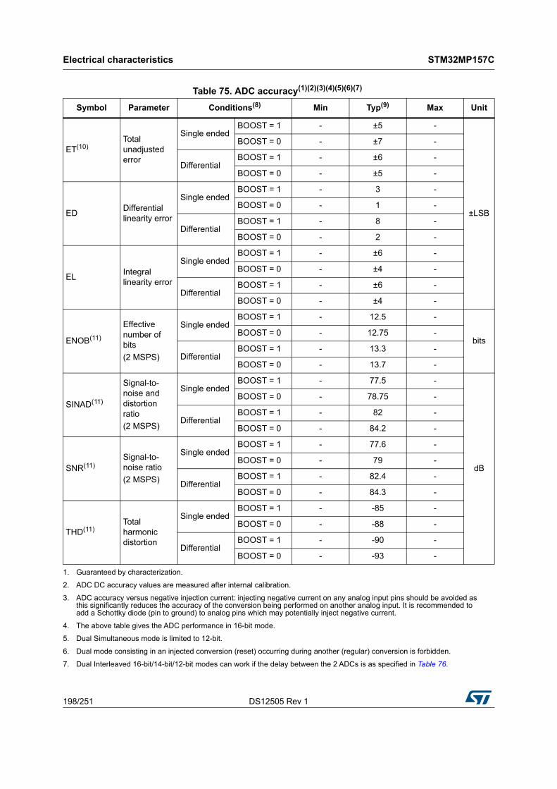
Electrical characteristics STM32MP157C
198/251 DS12505 Rev 1
Table 75. ADC accuracy(1)(2)(3)(4)(5)(6)(7)
Symbol Parameter Conditions(8) Min Typ(9) Max Unit
ET(10)Total unadjusted error
Single endedBOOST = 1 - ±5 -
±LSB
BOOST = 0 - ±7 -
DifferentialBOOST = 1 - ±6 -
BOOST = 0 - ±5 -
EDDifferential linearity error
Single endedBOOST = 1 - 3 -
BOOST = 0 - 1 -
DifferentialBOOST = 1 - 8 -
BOOST = 0 - 2 -
ELIntegral linearity error
Single endedBOOST = 1 - ±6 -
BOOST = 0 - ±4 -
DifferentialBOOST = 1 - ±6 -
BOOST = 0 - ±4 -
ENOB(11)
Effective number of bits
(2 MSPS)
Single endedBOOST = 1 - 12.5 -
bitsBOOST = 0 - 12.75 -
DifferentialBOOST = 1 - 13.3 -
BOOST = 0 - 13.7 -
SINAD(11)
Signal-to-noise and distortion ratio
(2 MSPS)
Single endedBOOST = 1 - 77.5 -
dB
BOOST = 0 - 78.75 -
DifferentialBOOST = 1 - 82 -
BOOST = 0 - 84.2 -
SNR(11)Signal-to-noise ratio
(2 MSPS)
Single endedBOOST = 1 - 77.6 -
BOOST = 0 - 79 -
DifferentialBOOST = 1 - 82.4 -
BOOST = 0 - 84.3 -
THD(11)Total harmonic distortion
Single endedBOOST = 1 - -85 -
BOOST = 0 - -88 -
DifferentialBOOST = 1 - -90 -
BOOST = 0 - -93 -
1. Guaranteed by characterization.
2. ADC DC accuracy values are measured after internal calibration.
3. ADC accuracy versus negative injection current: injecting negative current on any analog input pins should be avoided as this significantly reduces the accuracy of the conversion being performed on another analog input. It is recommended to add a Schottky diode (pin to ground) to analog pins which may potentially inject negative current.
4. The above table gives the ADC performance in 16-bit mode.
5. Dual Simultaneous mode is limited to 12-bit.
6. Dual mode consisting in an injected conversion (reset) occurring during another (regular) conversion is forbidden.
7. Dual Interleaved 16-bit/14-bit/12-bit modes can work if the delay between the 2 ADCs is as specified in Table 76.
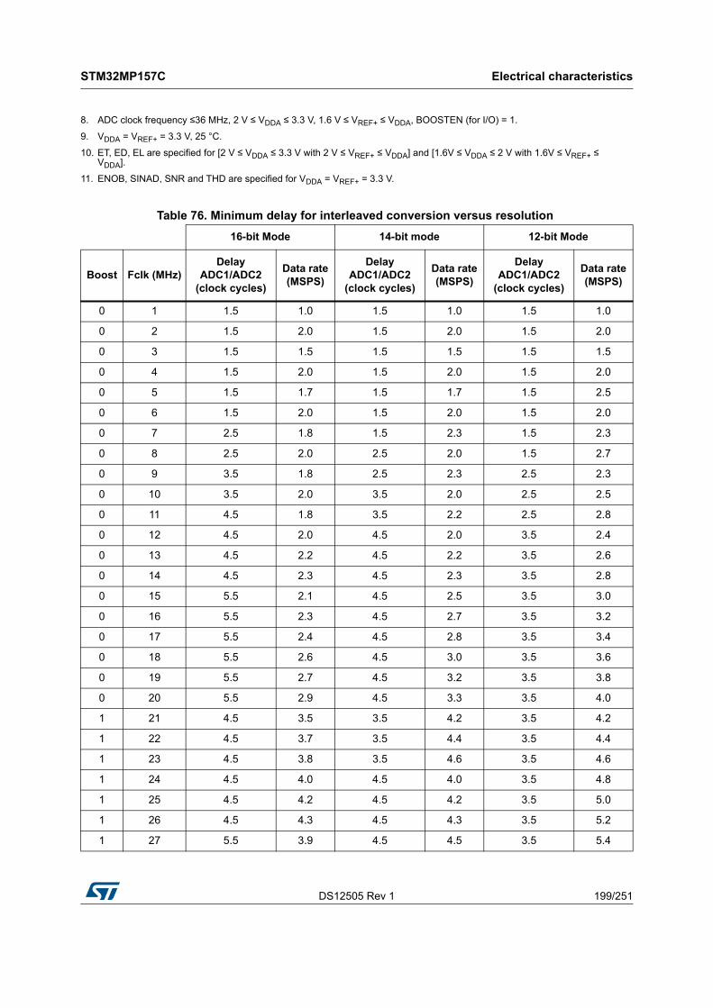
DS12505 Rev 1 199/251
STM32MP157C Electrical characteristics
234
8. ADC clock frequency ≤36 MHz, 2 V ≤ VDDA ≤ 3.3 V, 1.6 V ≤ VREF+ ≤ VDDA, BOOSTEN (for I/O) = 1.
9. VDDA = VREF+ = 3.3 V, 25 °C.
10. ET, ED, EL are specified for [2 V ≤ VDDA ≤ 3.3 V with 2 V ≤ VREF+ ≤ VDDA] and [1.6V ≤ VDDA ≤ 2 V with 1.6V ≤ VREF+ ≤ VDDA].
11. ENOB, SINAD, SNR and THD are specified for VDDA = VREF+ = 3.3 V.
Table 76. Minimum delay for interleaved conversion versus resolution
16-bit Mode 14-bit mode 12-bit Mode
Boost Fclk (MHz)Delay
ADC1/ADC2 (clock cycles)
Data rate (MSPS)
Delay ADC1/ADC2
(clock cycles)
Data rate (MSPS)
Delay ADC1/ADC2
(clock cycles)
Data rate (MSPS)
0 1 1.5 1.0 1.5 1.0 1.5 1.0
0 2 1.5 2.0 1.5 2.0 1.5 2.0
0 3 1.5 1.5 1.5 1.5 1.5 1.5
0 4 1.5 2.0 1.5 2.0 1.5 2.0
0 5 1.5 1.7 1.5 1.7 1.5 2.5
0 6 1.5 2.0 1.5 2.0 1.5 2.0
0 7 2.5 1.8 1.5 2.3 1.5 2.3
0 8 2.5 2.0 2.5 2.0 1.5 2.7
0 9 3.5 1.8 2.5 2.3 2.5 2.3
0 10 3.5 2.0 3.5 2.0 2.5 2.5
0 11 4.5 1.8 3.5 2.2 2.5 2.8
0 12 4.5 2.0 4.5 2.0 3.5 2.4
0 13 4.5 2.2 4.5 2.2 3.5 2.6
0 14 4.5 2.3 4.5 2.3 3.5 2.8
0 15 5.5 2.1 4.5 2.5 3.5 3.0
0 16 5.5 2.3 4.5 2.7 3.5 3.2
0 17 5.5 2.4 4.5 2.8 3.5 3.4
0 18 5.5 2.6 4.5 3.0 3.5 3.6
0 19 5.5 2.7 4.5 3.2 3.5 3.8
0 20 5.5 2.9 4.5 3.3 3.5 4.0
1 21 4.5 3.5 3.5 4.2 3.5 4.2
1 22 4.5 3.7 3.5 4.4 3.5 4.4
1 23 4.5 3.8 3.5 4.6 3.5 4.6
1 24 4.5 4.0 4.5 4.0 3.5 4.8
1 25 4.5 4.2 4.5 4.2 3.5 5.0
1 26 4.5 4.3 4.5 4.3 3.5 5.2
1 27 5.5 3.9 4.5 4.5 3.5 5.4
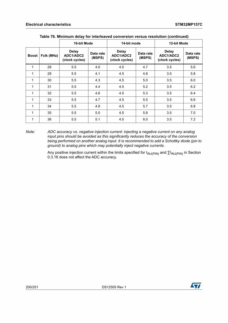
Electrical characteristics STM32MP157C
200/251 DS12505 Rev 1
Note: ADC accuracy vs. negative injection current: injecting a negative current on any analog input pins should be avoided as this significantly reduces the accuracy of the conversion being performed on another analog input. It is recommended to add a Schottky diode (pin to ground) to analog pins which may potentially inject negative currents.
Any positive injection current within the limits specified for IINJ(PIN) and ∑IINJ(PIN) in Section 0.3.16 does not affect the ADC accuracy.
1 28 5.5 4.0 4.5 4.7 3.5 5.6
1 29 5.5 4.1 4.5 4.8 3.5 5.8
1 30 5.5 4.3 4.5 5.0 3.5 6.0
1 31 5.5 4.4 4.5 5.2 3.5 6.2
1 32 5.5 4.6 4.5 5.3 3.5 6.4
1 33 5.5 4.7 4.5 5.5 3.5 6.6
1 34 5.5 4.9 4.5 5.7 3.5 6.8
1 35 5.5 5.0 4.5 5.8 3.5 7.0
1 36 5.5 5.1 4.5 6.0 3.5 7.2
Table 76. Minimum delay for interleaved conversion versus resolution (continued)
16-bit Mode 14-bit mode 12-bit Mode
Boost Fclk (MHz)Delay
ADC1/ADC2 (clock cycles)
Data rate (MSPS)
Delay ADC1/ADC2
(clock cycles)
Data rate (MSPS)
Delay ADC1/ADC2
(clock cycles)
Data rate (MSPS)
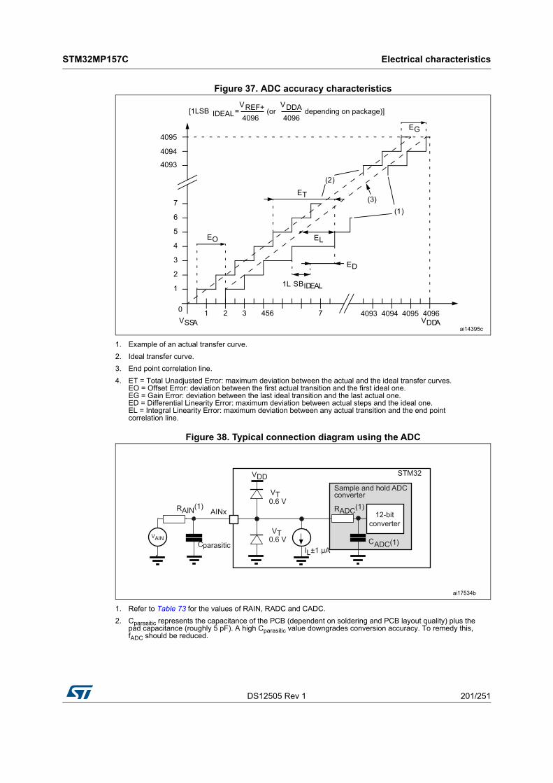
DS12505 Rev 1 201/251
STM32MP157C Electrical characteristics
234
Figure 37. ADC accuracy characteristics
1. Example of an actual transfer curve.
2. Ideal transfer curve.
3. End point correlation line.
4. ET = Total Unadjusted Error: maximum deviation between the actual and the ideal transfer curves. EO = Offset Error: deviation between the first actual transition and the first ideal one. EG = Gain Error: deviation between the last ideal transition and the last actual one. ED = Differential Linearity Error: maximum deviation between actual steps and the ideal one. EL = Integral Linearity Error: maximum deviation between any actual transition and the end point correlation line.
Figure 38. Typical connection diagram using the ADC
1. Refer to Table 73 for the values of RAIN, RADC and CADC.
2. Cparasitic represents the capacitance of the PCB (dependent on soldering and PCB layout quality) plus the pad capacitance (roughly 5 pF). A high Cparasitic value downgrades conversion accuracy. To remedy this, fADC should be reduced.
ai14395c
EO
EG
1L SBIDEAL
4095
4094
4093
5
4
3
2
1
0
7
6
1 2 3 456 7 4093 4094 4095 4096
(1)
(2)
ET
ED
EL
(3)
VDDAVSSA
VREF+4096
(or depending on package)]VDDA4096
[1LSB IDEAL =
ai17534b
STM32VDD
AINx
IL±1 μA0.6 VVT
RAIN(1)
CparasiticVAIN
0.6 VVT
RADC(1)
CADC(1)
12-bitconverter
Sample and hold ADC converter

Electrical characteristics STM32MP157C
202/251 DS12505 Rev 1
General PCB design guidelines
PCB design guidelines are provided in AN5031 “Getting started with STM32MP1 Series hardware development.” available from the ST website www.st.com.
6.3.22 DAC electrical characteristics
Table 77. DAC characteristics(1)
Symbol Parameter Conditions Min Typ Max Unit
VDDA Analog supply voltage - 1.8 3.3 3.6
VVREF+ Positive reference voltage - 1.80 - VDDA
VREF-Negative reference voltage
- - VSSA -
RL Resistive Load
DAC output buffer ON, Not valid in Sample & Hold mode
connected to VSSA
5 - -
kΩconnected to VDDA
25 - -
RO Output Impedance DAC output buffer OFF 10.3 13 16
RBON
Output impedance sample and hold mode, output buffer ON
DAC output buffer ON
VDD = 2.7 V - - 1.6kΩ
VDD = 2.0 V - - 2.6
RBOFF
Output impedance sample and hold mode, output buffer OFF
DAC output buffer OFF
VDD = 2.7 V - - 17.8kΩ
VDD = 2.0 V - - 18.7
CLCapacitive Load
DAC output buffer OFF - - 50 pF
CSH Sample and Hold mode - 0.1 1 µF
VDAC_OUTVoltage on DAC_OUT output
DAC output buffer ON 0.2 -VDDA -0.2(2)
V
DAC output buffer OFF 0 - VREF+
tSETTLING
Settling time (full scale: for a 12-bit code transition between the lowest and the highest input codes when DAC_OUT reaches the final value of ±0.5LSB, ±1LSB, ±2LSB, ±4LSB, ±8LSB)
Normal mode, DAC output buffer ON, CL ≤ 10 pF RL ≥ 5 kΩ
±0.5 LSB - TBD -
µs
±1 LSB - 2 -
±2 LSB - TBD -
±4 LSB - TBD -
±8 LSB - TBD -
Normal mode, DAC output buffer OFF, +/-1LSB, Cload ≤ 10 pF
- 2 -
tWAKEUP(3)
Wakeup time from off state (setting the Enx bit in the DAC Control register) until the ±1LSB final value
Normal mode, DAC output buffer ON, CL ≤ 50 pF, RL ≥ 5 kΩ
- 5 -
µsNormal mode, DAC output buffer OFF, CL ≤ 10 pF
2

DS12505 Rev 1 203/251
STM32MP157C Electrical characteristics
234
PSRRVDDA supply rejection ratio
Normal mode DAC output buffer ON CL ≤ 50 pF, RL = 5 kΩ DC
- -80 - dB
tSAMP
Sampling time in Sample and Hold mode
CSH=100nF
(Code transition between the lowest input code and the highest input code when DAC_OUT reaches final value ± 1LSB)
DACMCR.MODEx[2:0] = 100/101
(BUFFER ON)- 0.7 -
msDACMCR.MODEx[2:0] = 110
(BUFFER OFF)11.5
DACMCR.MODEx[2:0] = 111
(INTERNAL BUFFER OFF)- 0.3 -
CIintInternal sample and hold capacitor
- - 2.2 - µs
VoffsetMiddle code offset for 1 trim code step
VREF+ = 3.6 V - 450 -µV
VREF+ = 1.8 V - 213 -
IDDA(DAC)DAC quiescent
consumption from VDDA
DAC output buffer ON
No load, middle code (0x800)
- TBD -
µA
No load, worst code (0xF1C)
- TBD -
DAC output buffer OFF
No load, middle/worst code (0x800)
- TBD -
Sample and Hold mode, CSH = 100 nF
- TBD -
IDDV(DAC)DAC consumption from VREF+
DAC output buffer ON
No load, middle code (0x800)
- TBD -
No load, worst code (0xF1C)
- TBD -
DAC output buffer OFF
No load, middle/worst code (0x800)
- TBD -
Sample and Hold mode, Buffer ON, CSH = 100 nF (worst code)
- TBD -
Sample and Hold mode, Buffer OFF, CSH = 100 nF (worst code)
- TBD -
1. Guaranteed by design.
2. Since VREF+ must always be ≤ VDDA, maximum VDAC_OUT = minimum value between Max(VREF+) and Max(VDDA-0.2)
3. In buffered mode, the output can overshoot above the final value for low input code (starting from the minimum value).
Table 77. DAC characteristics(1) (continued)
Symbol Parameter Conditions Min Typ Max Unit
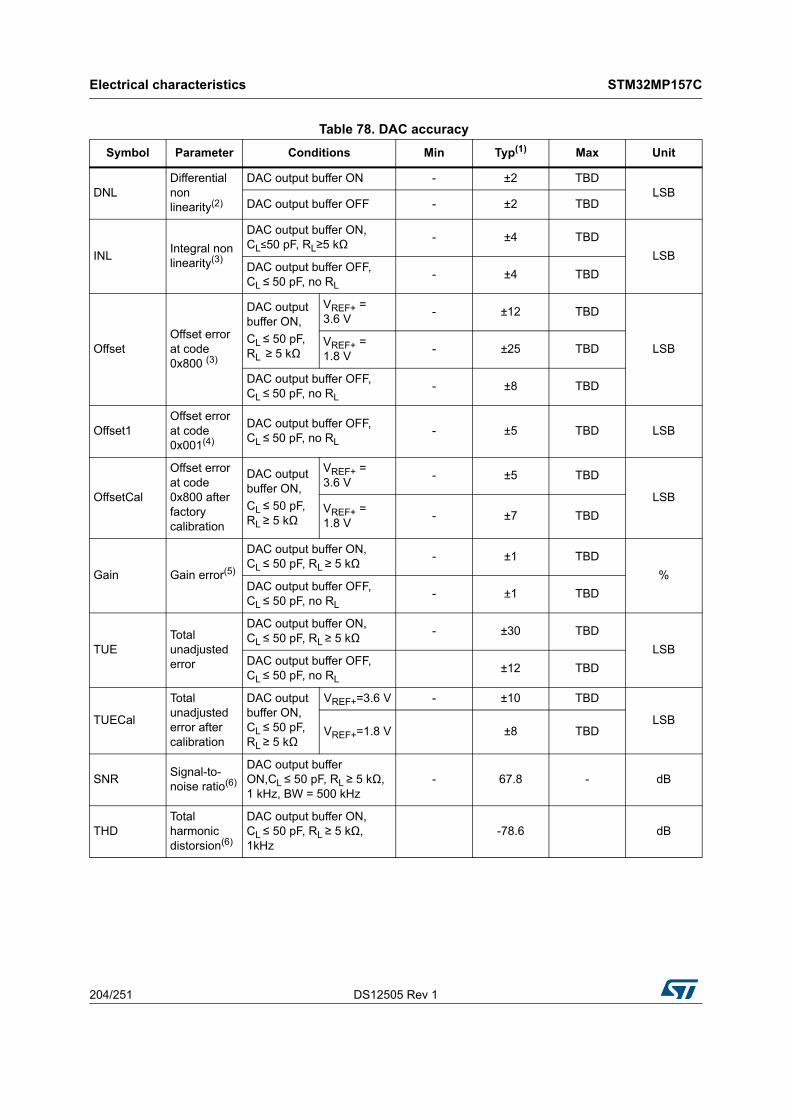
Electrical characteristics STM32MP157C
204/251 DS12505 Rev 1
Table 78. DAC accuracy
Symbol Parameter Conditions Min Typ(1) Max Unit
DNLDifferential non linearity(2)
DAC output buffer ON - ±2 TBDLSB
DAC output buffer OFF - ±2 TBD
INLIntegral non linearity(3)
DAC output buffer ON, CL≤50 pF, RL≥5 kΩ
- ±4 TBD
LSBDAC output buffer OFF, CL ≤ 50 pF, no RL
- ±4 TBD
OffsetOffset error at code 0x800 (3)
DAC output buffer ON,
CL ≤ 50 pF, RL ≥ 5 kΩ
VREF+ = 3.6 V
- ±12 TBD
LSBVREF+ = 1.8 V
- ±25 TBD
DAC output buffer OFF, CL ≤ 50 pF, no RL
- ±8 TBD
Offset1Offset error at code 0x001(4)
DAC output buffer OFF, CL ≤ 50 pF, no RL
- ±5 TBD LSB
OffsetCal
Offset error at code 0x800 after factory calibration
DAC output buffer ON,
CL ≤ 50 pF, RL ≥ 5 kΩ
VREF+ = 3.6 V
- ±5 TBD
LSBVREF+ = 1.8 V
- ±7 TBD
Gain Gain error(5)
DAC output buffer ON, CL ≤ 50 pF, RL ≥ 5 kΩ
- ±1 TBD
%DAC output buffer OFF, CL ≤ 50 pF, no RL
- ±1 TBD
TUETotal unadjusted error
DAC output buffer ON, CL ≤ 50 pF, RL ≥ 5 kΩ
- ±30 TBD
LSBDAC output buffer OFF, CL ≤ 50 pF, no RL
±12 TBD
TUECal
Total unadjusted error after calibration
DAC output buffer ON, CL ≤ 50 pF, RL ≥ 5 kΩ
VREF+=3.6 V - ±10 TBD
LSBVREF+=1.8 V ±8 TBD
SNRSignal-to-noise ratio(6)
DAC output buffer ON,CL ≤ 50 pF, RL ≥ 5 kΩ, 1 kHz, BW = 500 kHz
- 67.8 - dB
THDTotal harmonic distorsion(6)
DAC output buffer ON, CL ≤ 50 pF, RL ≥ 5 kΩ, 1kHz
-78.6 dB

DS12505 Rev 1 205/251
STM32MP157C Electrical characteristics
234
Figure 39. 12-bit buffered /non-buffered DAC
1. The DAC integrates an output buffer that can be used to reduce the output impedance and to drive external loads directly without the use of an external operational amplifier. The buffer can be bypassed by configuring the BOFFx bit in the DAC_CR register.
SINAD
Signal-to-noise and distortion ratio(6)
DAC output buffer ON, CL ≤ 50 pF, RL ≥ 5 kΩ, 1 kHz
- 67.5 - dB
ENOBEffective number of bits
DAC output buffer ON,
CL ≤ 50 pF, RL ≥ 5 kΩ, 1 kHz
- 10.9 - bits
1. Guaranteed by characterization.
2. Difference between two consecutive codes minus 1 LSB.
3. Difference between measured the value at Code i and the value measured at Code i on a line drawn between Code 0 and last Code 4095.
4. Difference between the value measured at Code (0x001) and the ideal value.
5. Difference between the ideal slope of the transfer function and the measured slope computed from code 0x000 and 0xFFF when the buffer is OFF, and from code giving 0.2 V and (VREF+ - 0.2 V) when the buffer is ON.
6. Signal is -0.5dBFS with Fsampling=1 MHz.
Table 78. DAC accuracy (continued)
Symbol Parameter Conditions Min Typ(1) Max Unit
R L
C L
Buffered/Non-buffered DAC
DAC_OUTx
Buffer(1)
12-bit digital to analog converter
ai17157V3
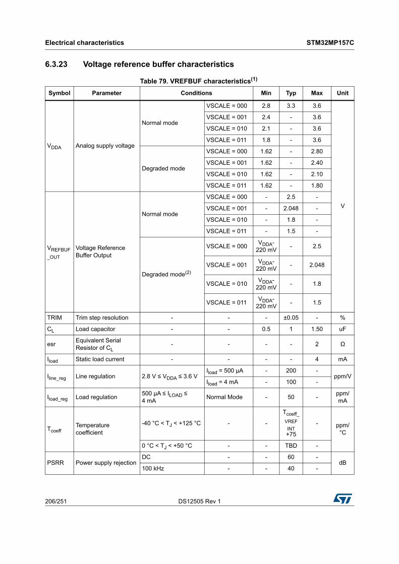
Electrical characteristics STM32MP157C
206/251 DS12505 Rev 1
6.3.23 Voltage reference buffer characteristics
Table 79. VREFBUF characteristics(1)
Symbol Parameter Conditions Min Typ Max Unit
VDDA Analog supply voltage
Normal mode
VSCALE = 000 2.8 3.3 3.6
V
VSCALE = 001 2.4 - 3.6
VSCALE = 010 2.1 - 3.6
VSCALE = 011 1.8 - 3.6
Degraded mode
VSCALE = 000 1.62 - 2.80
VSCALE = 001 1.62 - 2.40
VSCALE = 010 1.62 - 2.10
VSCALE = 011 1.62 - 1.80
VREFBUF
_OUT
Voltage Reference Buffer Output
Normal mode
VSCALE = 000 - 2.5 -
VSCALE = 001 - 2.048 -
VSCALE = 010 - 1.8 -
VSCALE = 011 - 1.5 -
Degraded mode(2)
VSCALE = 000VDDA-
220 mV- 2.5
VSCALE = 001VDDA-
220 mV- 2.048
VSCALE = 010VDDA-
220 mV- 1.8
VSCALE = 011VDDA-
220 mV- 1.5
TRIM Trim step resolution - - - ±0.05 - %
CL Load capacitor - - 0.5 1 1.50 uF
esrEquivalent Serial Resistor of CL
- - - - 2 Ω
Iload Static load current - - - - 4 mA
Iline_reg Line regulation 2.8 V ≤ VDDA ≤ 3.6 VIload = 500 µA - 200 -
ppm/VIload = 4 mA - 100 -
Iload_reg Load regulation500 µA ≤ ILOAD ≤ 4 mA
Normal Mode - 50 -ppm/mA
TcoeffTemperature coefficient
-40 °C < TJ < +125 °C - -
Tcoeff_
VREF
INT +75
- ppm/°C
0 °C < TJ < +50 °C - - TBD -
PSRR Power supply rejectionDC - - 60 -
dB100 kHz - - 40 -
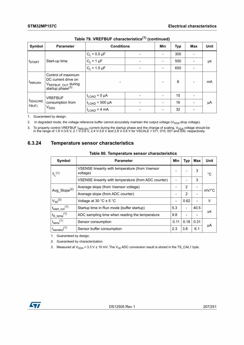
DS12505 Rev 1 207/251
STM32MP157C Electrical characteristics
234
6.3.24 Temperature sensor characteristics
tSTART Start-up time
CL = 0.5 µF - - 300 -
µsCL = 1 µF - - 500 -
CL = 1.5 µF - - 650 -
IINRUSH
Control of maximum DC current drive on VREFBUF_OUT during startup phase(3)
- - 8 - mA
IDDA(VRE
FBUF)
VREFBUF consumption from VDDA
ILOAD = 0 µA - - 15 -
µAILOAD = 500 µA - - 16 -
ILOAD = 4 mA - - 32 -
1. Guaranteed by design.
2. In degraded mode, the voltage reference buffer cannot accurately maintain the output voltage (VDDA-drop voltage).
3. To properly control VREFBUF IINRUSH current during the startup phase and the change of scaling, VDDA voltage should be in the range of 1.8 V-3.6 V, 2.1 V-3.6 V, 2.4 V-3.6 V and 2.8 V-3.6 V for VSCALE = 011, 010, 001 and 000, respectively.
Table 79. VREFBUF characteristics(1) (continued)
Symbol Parameter Conditions Min Typ Max Unit
Table 80. Temperature sensor characteristics
Symbol Parameter Min Typ Max Unit
TL(1)
1. Guaranteed by design.
VSENSE linearity with temperature (from Vsensor voltage)
- - 3°C
VSENSE linearity with temperature (from ADC counter) - - 3
Avg_Slope(2)
2. Guaranteed by characterization.
Average slope (from Vsensor voltage) - 2 -mV/°C
Average slope (from ADC counter) - 2 -
V30(3)
3. Measured at VDDA = 3.3 V ± 10 mV. The V30 ADC conversion result is stored in the TS_CAL1 byte.
Voltage at 30 °C ± 5 °C - 0.62 - V
tstart_run(1) Startup time in Run mode (buffer startup) 5.3 - 40.5
µstS_temp
(1) ADC sampling time when reading the temperature 9.8 - -
Isens(1) Sensor consumption 0.11 0.18 0.31
µAIsensbuf
(1) Sensor buffer consumption 2.3 3.8 6.1
Electrical characteristics STM32MP157C
208/251 DS12505 Rev 1
6.3.25 DTS characteristics
6.3.26 VBAT ADC monitoring characteristics and charging characteristics
Table 81. Temperature sensor calibration values
Symbol Parameter Memory address
TS_CAL1TS ADC raw data acquired at temperature of 30 °C ±5 °C VDDA = VREF+ = 3.3 V ±10 mV
0x5C00 525C[15:0](1)(2)
1. It is mandatory to read a 32-bit word and to do relevant masking and shifting to isolate the required bits.
2. This address is located inside the BSEC and the access is allowed after being enabled in the RCC.
TS_CAL2TS ADC raw data acquired at temperature of 130 °C ±2 °C VDDA = VREF+ = 3.3 V ±10 mV
0x5C00 525C[31:16](1)(2)
Table 82. DTS characteristics(1)
1. Guaranteed by design.
Symbol Parameter Conditions Min Typ Max Unit
fDTPOutput Clock frequency (PTAT dependency)
TBD TBD TBD kHz
TL
Linearity with temperature (from Output clock frequency). Temperature error at 1.1 V
TBD TBD TBD °C
TTOTAL_ ERROR
(2)
2. Guaranteed by characterization.
Temperature offset measurementTemperature:
-40 to 125 °CTBD TBD TBD °C
TVDD CORE
Additional error due to supply variation
- 10 - °C/V
tTRIM Calibration time 2 - - ms
tWAKE_UPWake-up time from off state until DTP ready signal = 1
- 50 - μs
IDDCORE_DTP DTP consumption on VDDCORE - 20 TBD µA
Table 83. VBAT ADC monitoring characteristics
Symbol Parameter Min Typ Max Unit
R Resistor bridge for VBAT - TBD - kΩ
Q Ratio on VBAT measurement - 4 - -
Er(1)
1. Guaranteed by design.
Error on Q –10 - +10 %
tS_vbat(1) ADC sampling time when reading VBAT input 9.8 - - µs

DS12505 Rev 1 209/251
STM32MP157C Electrical characteristics
234
6.3.27 Temperature and VBAT monitoring characteristics for temper detection
6.3.28 VDDCORE monitoring characteristics
6.3.29 Voltage booster for analog switch
Table 84. VBAT charging characteristics
Symbol Parameter Condition Min Typ Max Unit
RBC Battery charging resistorVBRS in PWR_CR3= 0 - 5 -
kΩ VBRS in PWR_CR3= 1 - 1.5 -
Table 85. Temperature and VBAT monitoring characteristics for temper detection
Symbol Parameter Min Typ Max Unit
TEMPhigh High temperature monitoring TBD 116 TBDoC
TEMPlow Low temperature monitoring TBD -31 TBD
VBAThigh High supply monitoring (with BKUPREGs ON) TBD 3.59 TBDV
VBATlow Low supply monitoring (with BKUPREGs ON) TBD 1.34 TBD
VBAThigh High supply monitoring (with BKUPREGs OFF) TBD 3.59 TBDV
VBATlow Low supply monitoring (with BKUPREGs OFF) TBD 1.34 TBD
Table 86. VDDCORE monitoring characteristics
Symbol Parameter Min Typ Max Unit
tS_vddcore(1)
1. Guaranteed by design.
ADC sampling time when reading VDDCORE input
100 - - ns
Table 87. Voltage booster for analog switch characteristics
Symbol Parameter Condition Min Typ Max Unit
VDD Supply voltage - 1.71 - 3.6 V
tSU(BOOST) Booster startup time - - - TBD µs
IDD(BOOST) Booster consumption 1.71 V ≤ VDD ≤ 2.7 V - - TBD
µA2.7 V < VDD < 3.6 V - - TBD

Electrical characteristics STM32MP157C
210/251 DS12505 Rev 1
6.3.30 Digital filter for sigma-delta modulators (DFSDM) characteristics
Unless otherwise specified, the parameters given in Table 88 for DFSDM are derived from tests performed under the ambient temperature, fpclkx frequency and VDD supply voltage summarized in Table 13: General operating conditions, with the following configuration:
• Output speed is set to OSPEEDRy[1:0] = 10
• Capacitive load C = 30 pF
• Measurement points are done at CMOS levels: 0.5×VDD
Refer to Section 0.3.16: I/O port characteristics for more details on the input/output alternate function characteristics (DFSDMx_CKINx, DFSDMx_DATINx, DFSDMx_CKOUT for DFSDMx).
Table 88. DFSDM measured timing
Symbol Parameter Conditions Min Typ Max Unit
fDFSDMCLK DFSDM clock 1.71 V < VDD < 3.6 V - - fSYSCLK
MHzfCKIN (1/TCKIN)
Input clock frequency
SPI mode (SITP[1:0]=0,1), External clock mode (SPICKSEL[1:0]=0), 1.71 V < VDD < 3.6 V
- -20
(fDFSDMCLK/4)
SPI mode (SITP[1:0]=0,1), External clock mode (SPICKSEL[1:0]=0), 2.7 < VDD < 3.6 V
- -20
(fDFSDMCLK/4)
SPI mode (SITP[1:0]=0,1), Internal clock mode (SPICKSEL[1:0]≠0), 1.71 < VDD < 3.6 V
- -20
(fDFSDMCLK/4)
SPI mode (SITP[1:0]=0,1), Internal clock mode (SPICKSEL[1:0]≠0), 2.7 < VDD < 3.6 V
- -20
(fDFSDMCLK/4)
fCKOUTOutput clock frequency
1.71 < VDD < 3.6 V - - 20
DuCyCKOUT
Output clock frequency duty cycle
1.71 < VDD < 3.6 V 45 50 55 %

DS12505 Rev 1 211/251
STM32MP157C Electrical characteristics
234
twh(CKIN) twl(CKIN)
Input clock high and low time
SPI mode (SITP[1:0]=0,1), External clock mode (SPICKSEL[1:0]=0), 1.71 < VDD < 3.6 V
TCKIN/2 - 0.5 TCKIN/2 -
ns
tsuData input setup time
SPI mode (SITP[1:0]=0,1), External clock mode (SPICKSEL[1:0]=0), 1.71 < VDD < 3.6 V
1 - -
thData input hold time
SPI mode (SITP[1:0]=0,1), External clock mode (SPICKSEL[1:0]=0), 1.71 < VDD < 3.6 V
0.5 - -
TManchester
Manchester data period (recovered clock period)
Manchester mode (SITP[1:0]=2,3), Internal clock mode (SPICKSEL[1:0]¹0), 1.71 < VDD < 3.6 V
(CKOUTDIV+1) ×TDFSDMCLK
(1) -(2×CKOUTDIV) × TDFSDMCLK
(1)
1. See DFSDM section in RM0436 reference manual for definition of CKOUTDIV.
Table 88. DFSDM measured timing (continued)
Symbol Parameter Conditions Min Typ Max Unit

Electrical characteristics STM32MP157C
212/251 DS12505 Rev 1
Figure 40. Channel transceiver timing diagrams
MS30766V2
SITP = 0
DFS
DM
_CK
OU
TD
FSD
M_D
ATIN
y
SITP = 1
tsu th
tsu th
tftrtwl twh
SP
I tim
ing
: SP
ICK
SE
L =
1, 2
, 3
recovered clock
SITP = 2
DFS
DM
_DAT
INy
SITP = 3
Man
ches
ter t
imin
g
recovered data 1 1 000
SITP = 00
DFS
DM
_CK
INy
DFS
DM
_DAT
INy
SITP = 01
tsu th
tsu th
tftrtwl twh
SP
I tim
ing
: SP
ICK
SE
L =
0
SPICKSEL=2
SPICKSEL=1
(SPICKSEL=0)
SPICKSEL=3
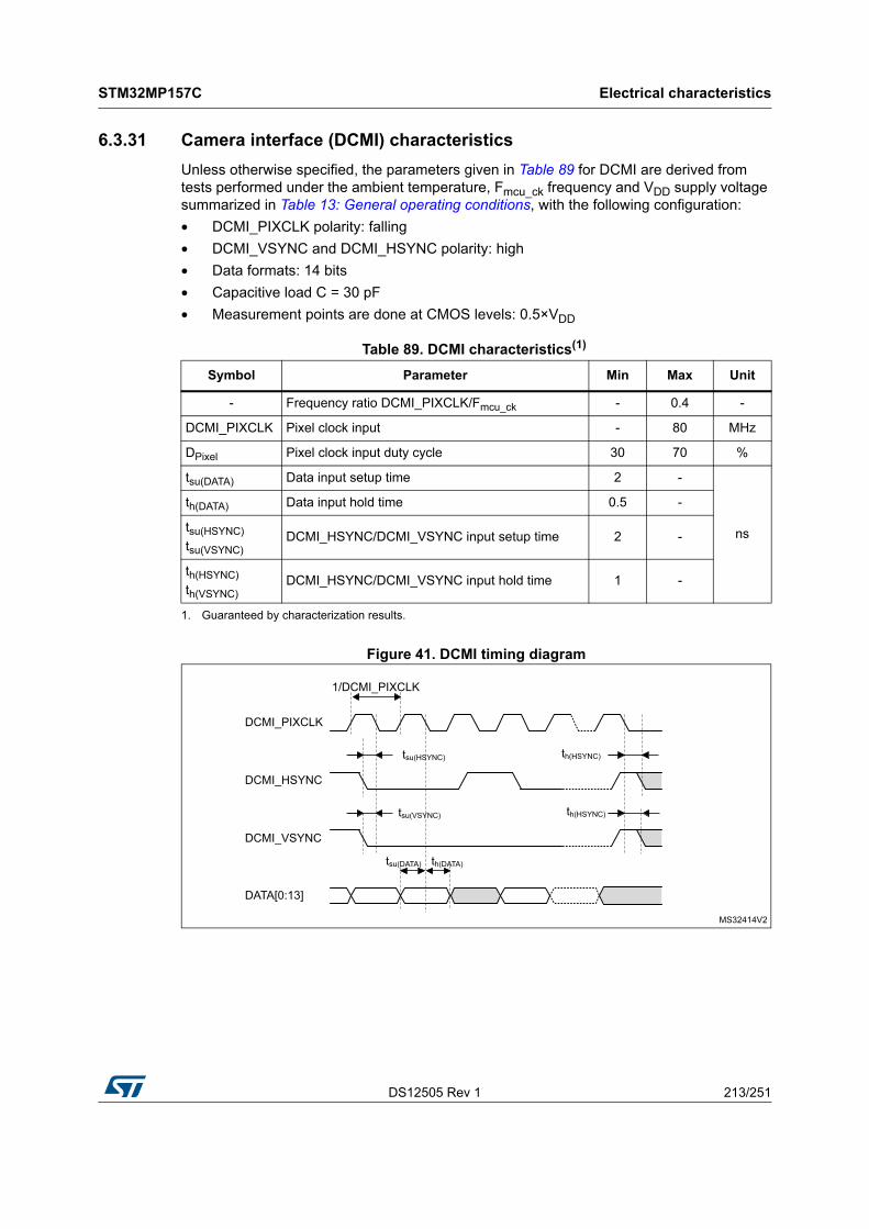
DS12505 Rev 1 213/251
STM32MP157C Electrical characteristics
234
6.3.31 Camera interface (DCMI) characteristics
Unless otherwise specified, the parameters given in Table 89 for DCMI are derived from tests performed under the ambient temperature, Fmcu_ck frequency and VDD supply voltage summarized in Table 13: General operating conditions, with the following configuration:
• DCMI_PIXCLK polarity: falling
• DCMI_VSYNC and DCMI_HSYNC polarity: high
• Data formats: 14 bits
• Capacitive load C = 30 pF
• Measurement points are done at CMOS levels: 0.5×VDD
Figure 41. DCMI timing diagram
Table 89. DCMI characteristics(1)
1. Guaranteed by characterization results.
Symbol Parameter Min Max Unit
- Frequency ratio DCMI_PIXCLK/Fmcu_ck - 0.4 -
DCMI_PIXCLK Pixel clock input - 80 MHz
DPixel Pixel clock input duty cycle 30 70 %
tsu(DATA) Data input setup time 2 -
ns
th(DATA) Data input hold time 0.5 -
tsu(HSYNC)
tsu(VSYNC)DCMI_HSYNC/DCMI_VSYNC input setup time 2 -
th(HSYNC)
th(VSYNC)DCMI_HSYNC/DCMI_VSYNC input hold time 1 -
MS32414V2
DCMI_PIXCLK
tsu(VSYNC)
tsu(HSYNC)
DCMI_HSYNC
DCMI_VSYNC
DATA[0:13]
1/DCMI_PIXCLK
th(HSYNC)
th(HSYNC)
tsu(DATA) th(DATA)

Electrical characteristics STM32MP157C
214/251 DS12505 Rev 1
6.3.32 LCD-TFT controller (LTDC) characteristics
Unless otherwise specified, the parameters given in Table 90 for LCD-TFT are derived from tests performed under the ambient temperature, Fpclk4 frequency and VDD supply voltage summarized in Table 13: General operating conditions, with the following configuration:
• LCD_CLK polarity: high
• LCD_DE polarity: low
• LCD_VSYNC and LCD_HSYNC polarity: high
• Pixel formats: 24 bits
• Output speed is set to OSPEEDRy[1:0] = 11
• Capacitive load C = 30 pF
• Measurement points are done at CMOS levels: 0.5×VDD
• I/O compensation cell enabled
Table 90. LTDC characteristics (1)
Symbol Parameter Conditions Min Max Unit
fCLK LTDC clock output frequency
2.7 V < VDD < 3.6 V OSPEEDR[1:0] = 11, 10
- 90
MHz1.71 V < VDD < 3.6 V OSPEEDR[1:0] = 11
- 45
1.71 V < VDD < 3.6 V OSPEEDR[1:0] = 10
- 38
DCLK LTDC clock output duty cycle - 45 55 %
tw(CLKH), tw(CLKL)
Clock High time, low time - tw(CLK)/2 - 0.5 tw(CLK)/2 + 0.5
ns
tv(DATA) Data output valid timeOSPEEDR[1:0] = 11 - 3
OSPEEDR[1:0] = 10 - 4
th(DATA) Data output hold time - 0 -
tv(HSYNC), tv(VSYNC), tv(DE)
HSYNC/VSYNC/DE output valid timeOSPEEDR[1:0] = 11 - 2.5
OSPEEDR[1:0] = 10 - 3.5
th(HSYNC), th(VSYNC), th(DE)
HSYNC/VSYNC/DE output hold time - 0 -
1. Guaranteed by characterization results.

DS12505 Rev 1 215/251
STM32MP157C Electrical characteristics
234
Figure 42. LCD-TFT horizontal timing diagram
Figure 43. LCD-TFT vertical timing diagram
MS32749V1
LCD_CLK
tv(HSYNC)
LCD_HSYNC
LCD_DE
LCD_R[0:7]LCD_G[0:7]LCD_B[0:7]
tCLK
LCD_VSYNC
tv(HSYNC)
tv(DE) th(DE)
Pixel1
Pixel2
tv(DATA)
th(DATA)
PixelN
HSYNCwidth
Horizontalback porch
Active width Horizontalback porch
One line
MS32750V1
LCD_CLK
tv(VSYNC)
LCD_R[0:7]LCD_G[0:7]LCD_B[0:7]
tCLK
LCD_VSYNC
tv(VSYNC)
M lines data
VSYNCwidth
Verticalback porch
Active width Verticalback porch
One frame
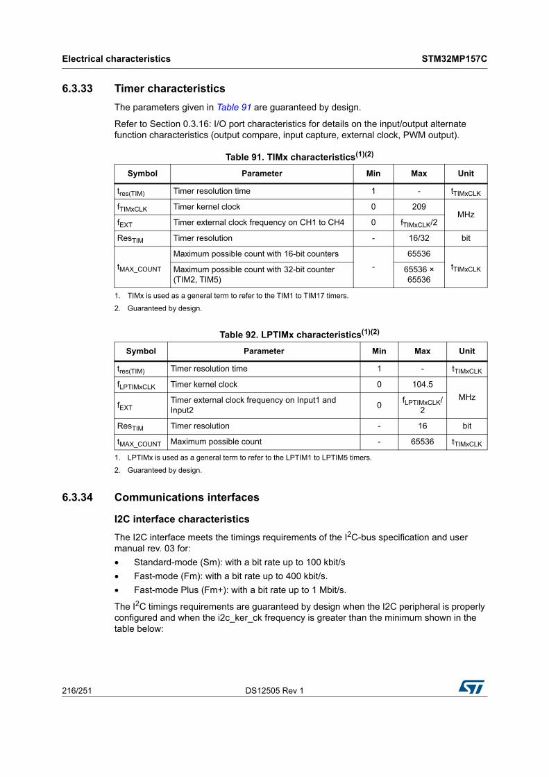
Electrical characteristics STM32MP157C
216/251 DS12505 Rev 1
6.3.33 Timer characteristics
The parameters given in Table 91 are guaranteed by design.
Refer to Section 0.3.16: I/O port characteristics for details on the input/output alternate function characteristics (output compare, input capture, external clock, PWM output).
6.3.34 Communications interfaces
I2C interface characteristics
The I2C interface meets the timings requirements of the I2C-bus specification and user manual rev. 03 for:
• Standard-mode (Sm): with a bit rate up to 100 kbit/s
• Fast-mode (Fm): with a bit rate up to 400 kbit/s.
• Fast-mode Plus (Fm+): with a bit rate up to 1 Mbit/s.
The I2C timings requirements are guaranteed by design when the I2C peripheral is properly configured and when the i2c_ker_ck frequency is greater than the minimum shown in the table below:
Table 91. TIMx characteristics(1)(2)
1. TIMx is used as a general term to refer to the TIM1 to TIM17 timers.
2. Guaranteed by design.
Symbol Parameter Min Max Unit
tres(TIM) Timer resolution time 1 - tTIMxCLK
fTIMxCLK Timer kernel clock 0 209MHz
fEXT Timer external clock frequency on CH1 to CH4 0 fTIMxCLK/2
ResTIM Timer resolution - 16/32 bit
tMAX_COUNT
Maximum possible count with 16-bit counters
-
65536
tTIMxCLKMaximum possible count with 32-bit counter (TIM2, TIM5)
65536 × 65536
Table 92. LPTIMx characteristics(1)(2)
1. LPTIMx is used as a general term to refer to the LPTIM1 to LPTIM5 timers.
2. Guaranteed by design.
Symbol Parameter Min Max Unit
tres(TIM) Timer resolution time 1 - tTIMxCLK
fLPTIMxCLK Timer kernel clock 0 104.5
MHzfEXT
Timer external clock frequency on Input1 and Input2
0fLPTIMxCLK/
2
ResTIM Timer resolution - 16 bit
tMAX_COUNT Maximum possible count - 65536 tTIMxCLK
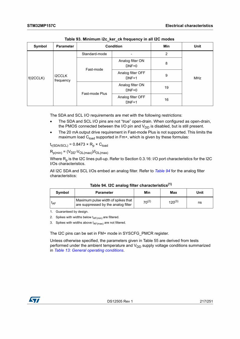
DS12505 Rev 1 217/251
STM32MP157C Electrical characteristics
234
The SDA and SCL I/O requirements are met with the following restrictions:
• The SDA and SCL I/O pins are not “true” open-drain. When configured as open-drain, the PMOS connected between the I/O pin and VDD is disabled, but is still present.
• The 20 mA output drive requirement in Fast-mode Plus is not supported. This limits the maximum load Cload supported in Fm+, which is given by these formulas:
tr(SDA/SCL) = 0.8473 × Rp × Cload
Rp(min) = (VDD-VOL(max))/IOL(max)
Where Rp is the I2C lines pull-up. Refer to Section 0.3.16: I/O port characteristics for the I2C I/Os characteristics.
All I2C SDA and SCL I/Os embed an analog filter. Refer to Table 94 for the analog filter characteristics:
The I2C pins can be set in FM+ mode in SYSCFG_PMCR register.
Unless otherwise specified, the parameters given in Table 55 are derived from tests performed under the ambient temperature and VDD supply voltage conditions summarized in Table 13: General operating conditions.
Table 93. Minimum i2c_ker_ck frequency in all I2C modes
Symbol Parameter Condition Min Unit
f(I2CCLK)I2CCLK frequency
Standard-mode - 2
MHz
Fast-mode
Analog filter ON
DNF=08
Analog filter OFF
DNF=19
Fast-mode Plus
Analog filter ON
DNF=019
Analog filter OFF
DNF=116
Table 94. I2C analog filter characteristics(1)
1. Guaranteed by design.
Symbol Parameter Min Max Unit
tAFMaximum pulse width of spikes that are suppressed by the analog filter
70(2)
2. Spikes with widths below tAF(min) are filtered.
120(3)
3. Spikes with widths above tAF(max) are not filtered.
ns

Electrical characteristics STM32MP157C
218/251 DS12505 Rev 1
SPI interface characteristics
Unless otherwise specified, the parameters given in Table 96 for the SPI interface are derived from tests performed under the ambient temperature, fpclkx frequency and VDD supply voltage conditions summarized in Table 13: General operating conditions, with the following configuration:
• Output speed is set to OSPEEDRy[1:0] = 11
• Capacitive load C = 30 pF
• Measurement points are done at CMOS levels: 0.5×VDD
• I/O compensation cell enabled
• HSLV activated when VDD ≤ 2.7 V
Refer to Section 0.3.16: I/O port characteristics for more details on the input/output alternate function characteristics (NSS, SCK, MOSI, MISO for SPI).
Table 95. I2C FM+ pin characteristics
Symbol Parameter Conditions Min Max Unit
Fmax(1)
1. The maximum frequency is defined with the following conditions: - (Tr + Tf) ≤ ⅔T - 45% < duty cycle < 55%.
Maximum frequency C = 50 pF 1.71 ≤ VDD ≤ 3.6 V
- 1 MHz
Tf(2)
2. The fall time is defined between 70% and 30% of the output waveform accordingl to I2C specification NXP UM10204 rev- Oct 2012.
Output high to low level fall time - 5 ns

DS12505 Rev 1 219/251
STM32MP157C Electrical characteristics
234
Table 96. SPI dynamic characteristics(1)
Symbol Parameter Conditions Min Typ Max Unit
fSCK SPI clock frequency
Master mode
1.71 V ≤ VDD ≤ 3.6 V
SPI1
- -
70
MHz
Master mode
2.7 V ≤ VDD ≤ 3.6 V
SPI1
80
Master mode
1.71 V ≤ VDD ≤ 3.6 V
SPI2, SPI3
80
Master mode
2.7 V ≤ VDD ≤ 3.6 V
SPI2, SPI3
100
Master mode
1.71 V ≤ VDD ≤ 3.6 V
SPI4, SPI5, SPI6
66
Slave receiver mode
1.71 V ≤ VDD ≤ 3.6 V
SPI1, SPI2, SPI3
100
Slave receiver mode
1.71 V ≤ VDD ≤ 3.6 V
SPI4, SPI5, SPI6
66
Slave mode transmitter/full duplex
2.7 V ≤ VDD ≤ 3.6 V38(2)
Slave mode transmitter/full duplex
1.71 V ≤ VDD ≤ 3.6 V35(2)
tsu(NSS) NSS setup timeSlave mode
2 - -
nsth(NSS) NSS hold time 1 - -
tw(SCKH), tw(SCKL)
SCK high and low time Master mode Tpclk - 1 Tpclk Tpclk + 1
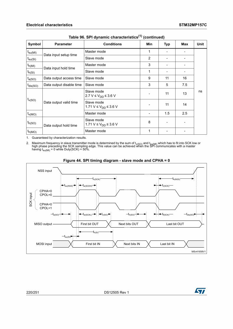
Electrical characteristics STM32MP157C
220/251 DS12505 Rev 1
Figure 44. SPI timing diagram - slave mode and CPHA = 0
tsu(MI)Data input setup time
Master mode 1 - -
ns
tsu(SI) Slave mode 2 - -
th(MI)Data input hold time
Master mode 3 - -
th(SI) Slave mode 1 - -
ta(SO) Data output access time Slave mode 9 11 16
tdis(SO) Data output disable time Slave mode 3 5 7.5
tv(SO)Data output valid time
Slave mode 2.7 V ≤ VDD ≤ 3.6 V
- 11 13
Slave mode 1.71 V ≤ VDD ≤ 3.6 V
- 11 14
tv(MO) Master mode - 1.5 2.5
th(SO)Data output hold time
Slave mode 1.71 V ≤ VDD ≤ 3.6 V
8 - -
th(MO) Master mode 1 - -
1. Guaranteed by characterization results.
2. Maximum frequency in slave transmitter mode is determined by the sum of tv(SO) and tsu(MI) which has to fit into SCK low or high phase preceding the SCK sampling edge. This value can be achieved when the SPI communicates with a master having tsu(MI) = 0 while Duty(SCK) = 50%.
Table 96. SPI dynamic characteristics(1) (continued)
Symbol Parameter Conditions Min Typ Max Unit
MSv41658V1
NSS input
CPHA=0CPOL=0
SC
K in
put
CPHA=0CPOL=1
MISO output
MOSI input
tsu(SI)
th(SI)
tw(SCKL)
tw(SCKH)
tc(SCK)
tr(SCK)
th(NSS)
tdis(SO)
tsu(NSS)
ta(SO) tv(SO)
Next bits IN
Last bit OUT
First bit IN
First bit OUT Next bits OUT
th(SO) tf(SCK)
Last bit IN

DS12505 Rev 1 221/251
STM32MP157C Electrical characteristics
234
Figure 45. SPI timing diagram - slave mode and CPHA = 1(1)
1. Measurement points are done at 0.5×VDD and with external CL = 30 pF.
Figure 46. SPI timing diagram - master mode(1)
1. Measurement points are done at 0.5×VDD and with external CL = 30 pF.
I2S interface characteristics
Unless otherwise specified, the parameters given in Table 97 for the I2S interface are derived from tests performed under the ambient temperature, fpclkx frequency and VDD
MSv41659V1
NSS input
CPHA=1CPOL=0
SC
K in
put
CPHA=1CPOL=1
MISO output
MOSI input
tsu(SI) th(SI)
tw(SCKL)
tw(SCKH)tsu(NSS)
tc(SCK)
ta(SO) tv(SO)
First bit OUT Next bits OUT
Next bits IN
Last bit OUT
th(SO) tr(SCK)
tf(SCK) th(NSS)
tdis(SO)
First bit IN Last bit IN
ai14136c
SC
K O
utpu
t
CPHA=0
MOSIOUTPUT
MISOINPUT
CPHA=0
LSB OUT
LSB IN
CPOL=0
CPOL=1
BIT1 OUT
NSS input
tc(SCK)
tw(SCKH)tw(SCKL)
tr(SCK)tf(SCK)
th(MI)
High
SC
K O
utpu
t
CPHA=1
CPHA=1
CPOL=0
CPOL=1
tsu(MI)
tv(MO) th(MO)
MSB IN BIT6 IN
MSB OUT

Electrical characteristics STM32MP157C
222/251 DS12505 Rev 1
supply voltage conditions summarized in Table 13: General operating conditions, with the following configuration:
• Output speed is set to OSPEEDRy[1:0] = 10
• Capacitive load C = 30 pF
• Measurement points are done at CMOS levels: 0.5×VDD
• I/O compensation cell enabled
Refer to Section 0.3.16: I/O port characteristics for more details on the input/output alternate function characteristics (CK, SD, WS).
Table 97. I2S dynamic characteristics(1)
Symbol Parameter Conditions Min Max Unit
fMCK I2S Main clock output - 256×8K 256×Fs MHz
fCK I2S clock frequency Master data - 64×Fs
MHzSlave data - 64×Fs
tv(WS) WS valid time Master mode - 6.5
ns
th(WS) WS hold time Master mode 0.5 -
tsu(WS) WS setup time Slave mode 1 -
th(WS) WS hold time Slave mode 0 -
tsu(SD_MR)Data input setup time
Master receiver 2 -
tsu(SD_SR) Slave receiver 1.5 -
th(SD_MR)Data input hold time
Master receiver 2 -
th(SD_SR) Slave receiver 0.5 -
tv(SD_ST)Data output valid time
Slave transmitter (after enable edge) - 15
tv(SD_MT) Master transmitter (after enable edge) - 1
th(SD_ST)Data output hold time
Slave transmitter (after enable edge) 8.5 -
th(SD_MT) Master transmitter (after enable edge) 0 -
1. Guaranteed by characterization results.
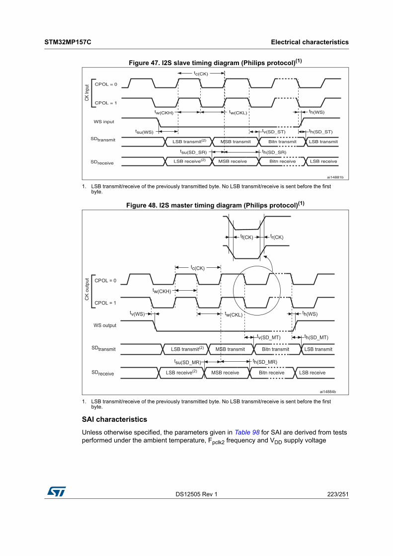
DS12505 Rev 1 223/251
STM32MP157C Electrical characteristics
234
Figure 47. I2S slave timing diagram (Philips protocol)(1)
1. LSB transmit/receive of the previously transmitted byte. No LSB transmit/receive is sent before the first byte.
Figure 48. I2S master timing diagram (Philips protocol)(1)
1. LSB transmit/receive of the previously transmitted byte. No LSB transmit/receive is sent before the first byte.
SAI characteristics
Unless otherwise specified, the parameters given in Table 98 for SAI are derived from tests performed under the ambient temperature, Fpclk2 frequency and VDD supply voltage
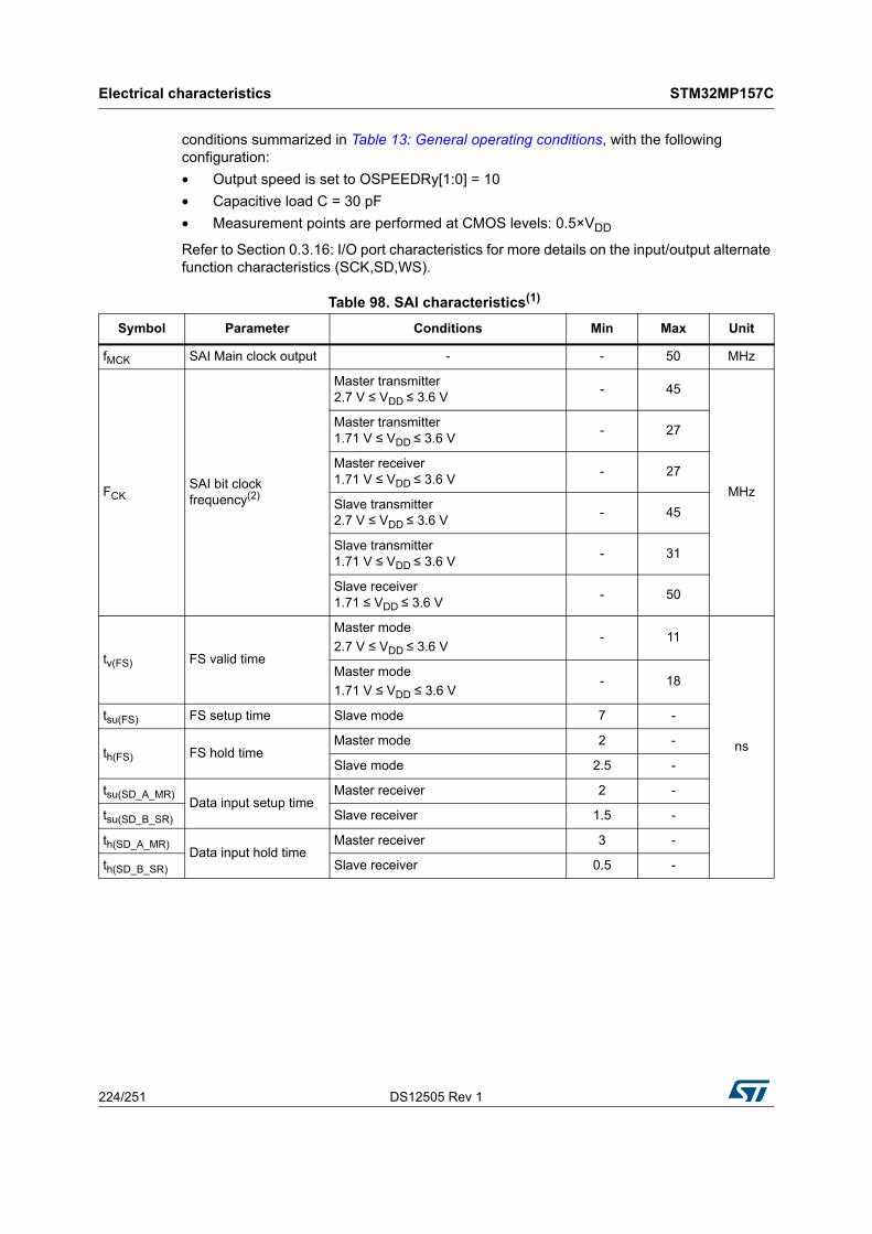
Electrical characteristics STM32MP157C
224/251 DS12505 Rev 1
conditions summarized in Table 13: General operating conditions, with the following configuration:
• Output speed is set to OSPEEDRy[1:0] = 10
• Capacitive load C = 30 pF
• Measurement points are performed at CMOS levels: 0.5×VDD
Refer to Section 0.3.16: I/O port characteristics for more details on the input/output alternate function characteristics (SCK,SD,WS).
Table 98. SAI characteristics(1)
Symbol Parameter Conditions Min Max Unit
fMCK SAI Main clock output - - 50 MHz
FCKSAI bit clock frequency(2)
Master transmitter 2.7 V ≤ VDD ≤ 3.6 V
- 45
MHz
Master transmitter 1.71 V ≤ VDD ≤ 3.6 V
- 27
Master receiver 1.71 V ≤ VDD ≤ 3.6 V
- 27
Slave transmitter 2.7 V ≤ VDD ≤ 3.6 V
- 45
Slave transmitter 1.71 V ≤ VDD ≤ 3.6 V
- 31
Slave receiver 1.71 ≤ VDD ≤ 3.6 V
- 50
tv(FS) FS valid time
Master mode
2.7 V ≤ VDD ≤ 3.6 V- 11
ns
Master mode
1.71 V ≤ VDD ≤ 3.6 V- 18
tsu(FS) FS setup time Slave mode 7 -
th(FS) FS hold time Master mode 2 -
Slave mode 2.5 -
tsu(SD_A_MR)Data input setup time
Master receiver 2 -
tsu(SD_B_SR) Slave receiver 1.5 -
th(SD_A_MR)Data input hold time
Master receiver 3 -
th(SD_B_SR) Slave receiver 0.5 -

DS12505 Rev 1 225/251
STM32MP157C Electrical characteristics
234
Figure 49. SAI master timing waveforms
Figure 50. SAI slave timing waveforms
tv(SD_B_ST) Data output valid time
Slave transmitter (after enable edge)
2.7 V ≤ VDD ≤ 3.6 V- 11
ns
Slave transmitter (after enable edge)
1.71 V ≤ VDD ≤ 3.6 V- 16
th(SD_B_ST) Data output hold time Slave transmitter (after enable edge) 8.5 -
tv(SD_A_MT) Data output valid time
Master transmitter (after enable edge)
2.7 V ≤ VDD ≤ 3.6 V- 10
Master transmitter (after enable edge)
1.71 V ≤ VDD ≤ 3.6 V- 18
th(SD_A_MT) Data output hold time Master transmitter (after enable edge) 7 -
1. Guaranteed by characterization results.
2. APB clock frequency must be at least twice SAI clock frequency.
Table 98. SAI characteristics(1) (continued)
Symbol Parameter Conditions Min Max Unit
MS32771V1
SAI_SCK_X
SAI_FS_X(output)
1/fSCK
SAI_SD_X(transmit)
tv(FS)
Slot n
SAI_SD_X(receive)
th(FS)
Slot n+2
tv(SD_MT) th(SD_MT)
Slot n
tsu(SD_MR) th(SD_MR)
MS32772V1
SAI_SCK_X
SAI_FS_X(input)
SAI_SD_X(transmit)
tsu(FS)
Slot n
SAI_SD_X(receive)
tw(CKH_X) th(FS)
Slot n+2
tv(SD_ST) th(SD_ST)
Slot n
tsu(SD_SR)
tw(CKL_X)
th(SD_SR)

Electrical characteristics STM32MP157C
226/251 DS12505 Rev 1
MDIOS characteristics
The MDIOS controller is mapped on APB1 domain. The frequency of the APB bus should at least 1.5 times the MDC frequency: Fpclk1 ≥ 1.5 * FMDC.
Figure 51. MDIOS timing diagram
SD/SDIO MMC card host interface (SDMMC) characteristics
Unless otherwise specified, the parameters given in Table 100 for the SDIO/MMC interface are derived from tests performed under the ambient temperature, Fhclk6 frequency and VDD supply voltage conditions summarized in Table 13: General operating conditions, with the following configuration:
• Output speed is set to OSPEEDRy[1:0] = 11
• Capacitive load C = 30 pF
• Measurement points are done at CMOS levels: 0.5×VDD
• I/O compensation cell enabled
• HSLV activated when VDD ≤ 2.7 V
• Delay block disabled
Refer to Section 0.3.16: I/O port characteristics for more details on the input/output characteristics.
Table 99. MDIOS timing parameters
Symbol Parameter Min Typ Max Unit
FMDC Management data clock - - 30 MHz
td(MDIOS) Management data input/output output valid time 6.5 8 19
nstsu(MDIOS) Management data input/output setup time 1 - -
th(MDIOS) Management data input/output hold time 0.5 - -
MSv50900V1
tsu(MDIOS)
TMDC
th(MDIOS)
td(MDIOS)
MDIOS_MDC
MDIOS_MDIO(I)
MDIOS_MDIO(O)

DS12505 Rev 1 227/251
STM32MP157C Electrical characteristics
234
Table 100. Dynamic characteristics: SD / MMC / e•MMC characteristics, VDD = 2.7 V to 3.6 V(1)(2)
Symbol Parameter Conditions Min Typ Max Unit
fPP Clock frequency in data transfer mode - 0 - 130 MHz
- SDIO_CK/fpclk2 frequency ratio - - - 8/3 -
tW(CKL) Clock low timefPP = 52 MHz
8.5 9.5 -ns
tW(CKH) Clock high time 8.5 9.5 -
CMD, D inputs (referenced to CK) in MMC and SD HS/SDR(3)/DDR(3) mode
tISU Input setup time HS
-
1.5 - -
nstIH Input hold time HS 1.5 - -
tIDW(4) Input valid window (variable window) 2.5 - -
CMD, D outputs (referenced to CK) in MMC and SD HS/SDR(3)/DDR(3) mode
tOV Output valid time HS-
- 5 6.5ns
tOH Output hold time HS 2.5 - -
CMD, D inputs (referenced to CK) in SD default mode
tISUD Input setup time SD-
1.5 - -ns
tIHD Input hold time SD 1.5 - -
CMD, D outputs (referenced to CK) in SD default mode
tOVD Output valid default time SD-
- 0.5 1.5ns
tOHD Output hold default time SD 0 - -
1. Guaranteed by characterization results.
2. Above 100 MHz, CL = 20 pF.
3. For SD 1.8 V support, an external voltage converter is required.
4. The minimum window of time where the data needs to be stable for proper sampling in tuning mode.
Table 101. Dynamic characteristics: SD / MMC / e•MMC characteristicsVDD = 1.71 V to 1.9 V(1)(2)
Symbol Parameter Conditions Min Typ Max Unit
fPP Clock frequency in data transfer mode - 0 - 105 MHz
- SDIO_CK/fpclk2 frequency ratio - - - 8/3 -
tW(CKL) Clock low timefPP = 52 MHz
8.5 9.5 -ns
tW(CKH) Clock high time 8.5 9.5 -
CMD, D inputs (referenced to CK) in e•MMC mode
tISU Input setup time HS
-
1.5 - -
nstIH Input hold time HS 2.5 - -
tIDW(3) Input valid window (variable window) 3 - -
CMD, D outputs (referenced to CK) in e•MMC mode
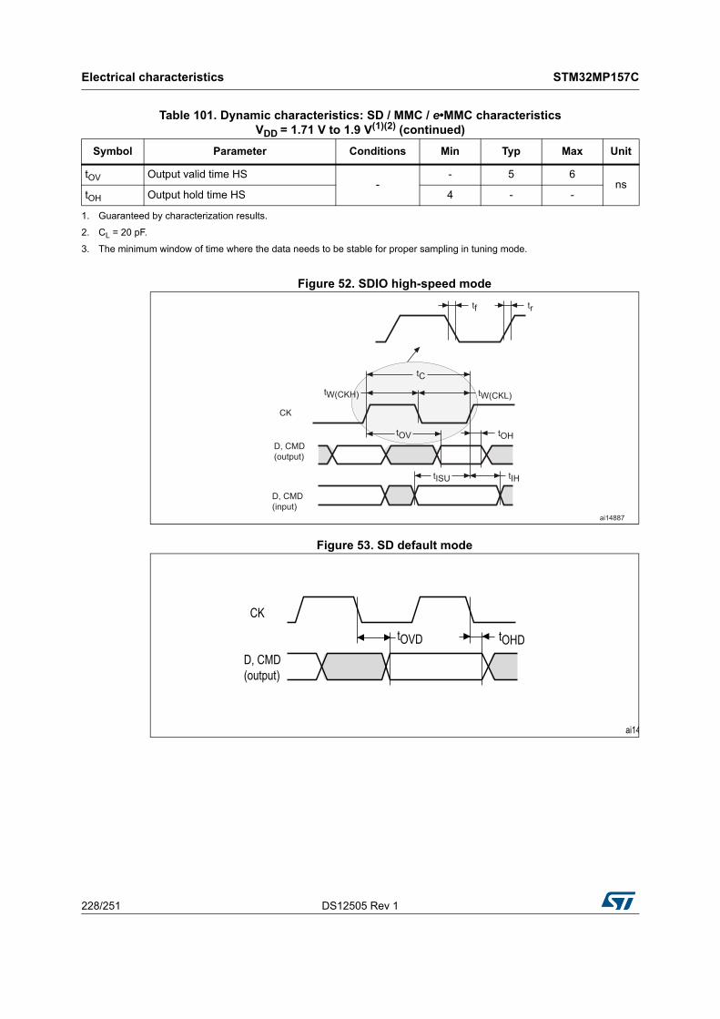
Electrical characteristics STM32MP157C
228/251 DS12505 Rev 1
Figure 52. SDIO high-speed mode
Figure 53. SD default mode
tOV Output valid time HS-
- 5 6ns
tOH Output hold time HS 4 - -
1. Guaranteed by characterization results.
2. CL = 20 pF.
3. The minimum window of time where the data needs to be stable for proper sampling in tuning mode.
Table 101. Dynamic characteristics: SD / MMC / e•MMC characteristicsVDD = 1.71 V to 1.9 V(1)(2) (continued)
Symbol Parameter Conditions Min Typ Max Unit
ai14
CK
D, CMD(output)
tOVD tOHD

DS12505 Rev 1 229/251
STM32MP157C Electrical characteristics
234
Figure 54. DDR mode
FDCAN (controller area network) interface
Refer to Section 6.3.16: I/O port characteristics for more details on the input/output alternate function characteristics (FDCANx_TX and FDCANx_RX).
USB OTG_FS characteristics
The USB interface is fully compliant with the USB specification version 2.0 and is USB-IF certified (for Full-speed device operation).
Ethernet (ETH) characteristics
Unless otherwise specified, the parameters given in Table 103, Table 104, Table 105, Table 106 and Table 107 for MDIO/SMA, RMII, GMII, RGMII and MII are derived from tests performed under the ambient temperature, Faxiss_ck frequency summarized in Table 13: General operating conditions, with the following configuration:
• Output speed is set to OSPEEDRy[1:0] = 10
• Capacitive load C = 20 pF
• Measurement points are done at CMOS levels: 0.5×VDD.
Refer to Section 0.3.16: I/O port characteristics for more details on the input/output characteristics.
MSv36879V1
Data output D0 D2 D4
Clock
Data input D0 D2 D4
t(CK) tw(CKH) tw(CKL)tr(CK) tf(CK)
tsf(IN) thf(IN)
tvf(OUT) thr(OUT)
D1 D3 D5
D1 D3 D5
tvr(OUT) thf(OUT)
tsr(IN) thr(IN)
Table 102. USB OTG_FS electrical characteristics
Symbol Parameter Condition Min Typ Max Unit
VDD33USBUSB transceiver operating voltage
- 3.0(1) - 3.6 V
RPUI Embedded USB_DP pull-up value during idle
- 900 1250 1600
ΩRPUR
Embedded USB_DP pull-up value during reception
- 1400 2300 3200
ZDRV Output driver impedance(2) Driver high and low 28 36 44
1. The USB functionality is ensured down to 2.7 V but not the full USB electrical characteristics which are degraded in the 2.7 to 3.0 V voltage range.
2. No external termination series resistors are required on USB_DP (D+) and USB_DM (D-); the matching impedance is already included in the embedded driver.

Electrical characteristics STM32MP157C
230/251 DS12505 Rev 1
Table 103 gives the list of Ethernet MAC timings for the MDIO/SMA and Figure 55 shows the corresponding timing diagram.
Figure 55. Ethernet MDIO/SMA timing diagram
Table 104 gives the list of Ethernet MAC timings for the RMII and Figure 56 shows the corresponding timing diagram.
Table 103. Dynamics characteristics: Ethernet MAC timings for MDIO/SMA(1)
1. Guaranteed by characterization results.
Symbol Parameter Min Typ Max Unit
tMDC MDC cycle time(2.5 MHz) 399 400 401
nsTd(MDIO) Write data valid time 0.5 1 3
tsu(MDIO) Read data setup time 13.5 - -
th(MDIO) Read data hold time 0 - -
Table 104. Dynamics characteristics: Ethernet MAC timings for RMII(1)
1. Guaranteed by characterization results.
Symbol Parameter Min Typ Max Unit
tsu(RXD) Receive data setup time 2 - -
ns
tih(RXD) Receive data hold time 1.5 - -
tsu(CRS) Carrier sense setup time 1.5 - -
tih(CRS) Carrier sense hold time 1.5 - -
td(TXEN) Transmit enable valid delay time 5.5 6.5 9.5
td(TXD) Transmit data valid delay time 6 6.5 10
MS31384V1
ETH_MDC
ETH_MDIO(O)
ETH_MDIO(I)
tMDC
td(MDIO)
tsu(MDIO) th(MDIO)

DS12505 Rev 1 231/251
STM32MP157C Electrical characteristics
234
Figure 56. Ethernet RMII timing diagram
Table 105 gives the list of Ethernet MAC timings for MII and Figure 57 shows the corresponding timing diagram.
Table 105. Dynamics characteristics: Ethernet MAC timings for MII(1)
1. Guaranteed by characterization results.
Symbol Parameter Min Typ Max Unit
tsu(RXD) Receive data setup time 2 - -
ns
tih(RXD) Receive data hold time 1 - -
tsu(DV) Data valid setup time 1 - -
tih(DV) Data valid hold time 0.5 - -
tsu(ER) Error setup time 1 - -
tih(ER) Error hold time 0.5 - -
td(TXEN) Transmit enable valid delay time 6 7.5 10.5
td(TXD) Transmit data valid delay time 7 8 11
ai15667b
RMII_REF_CLK
RMII_TX_ENRMII_TXD[1:0]
RMII_RXD[1:0]RMII_CRS_DV
td(TXEN)td(TXD)
tsu(RXD)tsu(CRS)
tih(RXD)tih(CRS)
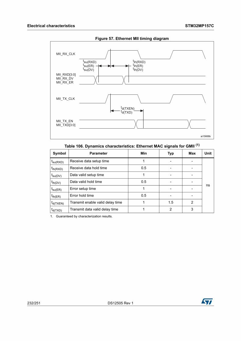
Electrical characteristics STM32MP157C
232/251 DS12505 Rev 1
Figure 57. Ethernet MII timing diagram
Table 106. Dynamics characteristics: Ethernet MAC signals for GMII (1)
1. Guaranteed by characterization results.
Symbol Parameter Min Typ Max Unit
tsu(RXD) Receive data setup time 1 - -
ns
tih(RXD) Receive data hold time 0.5 - -
tsu(DV) Data valid setup time 1 - -
tih(DV) Data valid hold time 0.5 - -
tsu(ER) Error setup time 1 - -
tih(ER) Error hold time 0.5 - -
td(TXEN) Transmit enable valid delay time 1 1.5 2
td(TXD) Transmit data valid delay time 1 2 3
ai15668b
MII_RX_CLK
MII_RXD[3:0]MII_RX_DVMII_RX_ER
td(TXEN)td(TXD)
tsu(RXD)tsu(ER)tsu(DV)
tih(RXD)tih(ER)tih(DV)
MII_TX_CLK
MII_TX_ENMII_TXD[3:0]

DS12505 Rev 1 233/251
STM32MP157C Electrical characteristics
234
Figure 58. Ethernet GMII timing diagram
Figure 59. Ethernet RGMII timing diagram
Table 107. Dynamics characteristics: Ethernet MAC signals for RGMII (1)
1. Guaranteed by characterization results.
Symbol Rating Min Typ Max Unit
tsu(RXD) Receive data setup time 1.12(2)
2. Guaranteed by design.
- -
ns
tih(RXD) Receive data hold time 0.83(2) - -
tsu(DV) Data valid setup time 1.12(2) - -
tih(DV) Data valid hold time 0.83(2) - -
TskewT(TXEN) Transmit enable valid delay time -0.25 0.25 0.5
TskewT(TXD) Transmit data valid delay time -0.25 2 0.5
MSv50970V1
GMII_TX_ENGMII_TXD[7:0]
GTX_CLK
GMII_RXD[7:0]GMII_RX_DVGMII_RX_ER
GMII_RX_CLK
tsu(RXD)tsu(ER)tsu(DV)
tih(RXD)tih(ER)tih(DV)
td(TXEN)td(TXD)
MSv50971V1
RGMII_RXD[3:0]RGMII_RX_DV
RGMII_RX_CLK
RGMII_TXD[3:0]RGMII_TX_EN
RGMII_GTX_CLK
tsu
tskewT
tih

Electrical characteristics STM32MP157C
234/251 DS12505 Rev 1
6.3.35 USART interface characteristics
Unless otherwise specified, the parameters given in Table 108 for USART are derived from tests performed under the ambient temperature, fHCLK frequency and VDD supply voltage conditions summarized in Table 108, with the following configuration:
• Output speed is set to OSPEEDRy[1:0] = 10
• Capacitive load C = 30 pF
• Measurement points are done at CMOS levels: 0.5×VDD
Refer to Section 6.3.16: I/O port characteristics for more details on the input/output alternate function characteristics (NSS, CK, TX, RX for USART).
Table 108. USART characteristics(1)
Symbol Parameter Conditions Min Typ Max Unit
fCK USART clock frequency
Master mode
USART2,3,6- -
12.5
MHzMaster mode
USART116.5
Slave mode - - 27
tsu(NSS) NSS setup time Slave mode tker+2 - - ns
th(NSS) NSS hold time Slave mode 2 - - ns
tw(CKH), tw(CKL)
CK high and low time Master mode 1/fCK/2 - 1 1/fck/2 1/fCK/2 + 1 ns
tsu(RX) Data input setup timeMaster mode tker+3 - -
nsSlave mode 2 - -
thRX) Data input hold timeMaster mode 1 - -
nsSlave mode 1 - -
tv(TX) Data output valid timeSlave mode - 10 18
nsMaster mode - 0.5 1
th(TX) Data output hold timeSlave mode 8 - -
nsMaster mode 0 - -
1. 1.Guaranteed by characterization results.

DS12505 Rev 1 235/251
STM32MP157C Package information
248
7 Package information
In order to meet environmental requirements, ST offers these devices in different grades of ECOPACK® packages, depending on their level of environmental compliance. ECOPACK® specifications, grade definitions and product status are available at: www.st.com. ECOPACK® is an ST trademark.
7.1 TFBGA 257 package information
Figure 60. TFBGA - 257 balls, 10x10 mm, 0.5/0.65 mm pitch, low profile fine pitchball grid array package outline
1. Drawing is not to scale.
B02Y_ME_V1
D
E
F1
e1
e2
F2
E2E1
F1
e2F2D2
D1
Peripheral ball m
atrix pitch 0.5 mm
K
H
D
ABC
EFG
J
LMNPR
UT
VW
A
B
1H
1D
1A1B1C
1E1F1G
1JC
entral ball matrix pitch 0.65 m
m
Peripheral ball matrix pitch 0.5 mm
Central ball matrix pitch 0.65 mm
12
34
56
78
910
1112
15 131416
1718
19
12
34
56
78
9
A1 ball pad corner
b (257 balls)eee M C A Bfff M C
AA1A2
SEATING PLANE
C
ddd C
BOTTOM VIEW TOP VIEW
SIDE VIEW
e1

Package information STM32MP157C
236/251 DS12505 Rev 1
Table 109. TFBGA - 257 balls, 10x10 mm, 0.5/0.65 mm pitch, low profile fine pitchball grid array mechanical data
Symbolmillimeters inches(1)
1. Values in inches are converted from mm and rounded to 4 decimal digits.
Min Typ Max Min Typ Max
A - - 1.200 - - 0.0472
A1(2)
2. - The terminal A1 corner must be identified on the top surface by using a corner chamfer, ink or metalized markings, or other feature of package body or integral heat slug. - A distinguishing feature is allowable on the bottom surface of the package to identify the terminal A1 corner. Exact shape of each corner is optional.
0.150 - - 0.0059 - -
A2 - 0.810 - - 0.0319 -
b(3)
3. Initial ball equal 0.300 mm.
0.300 0.350 0.400 0.0118 0.0138 0.0157
D 9.850 10.000 10.150 0.3878 0.3937 0.3996
D1 - 9.000 - - 0.3543 -
E 9.850 10.000 10.150 0.3878 0.3937 0.3996
E1 - 9.000 - - 0.3543 -
D2 - 5.200 - - 0.2047 -
E2 - 5.200 - - 0.2047 -
e1 - 0.500 - - 0.0197 -
e2 - 0.650 - - 0.0256 -
F1 - 0.500 - - 0.0197 -
F2 - 2.400 - - 0.0945 -
ddd - - 0.100 - - 0.0039
eee(4)
4. The tolerance of position that controls the location of the pattern of balls with respect to datums A and B. For each ball there is a cylindrical tolerance zone eee perpendicular to datum C and located on true position with respect to datums A and B as defined by e. The axis perpendicular to datum C of each ball must lie within this tolerance zone.
- - 0.150 - - 0.0059
fff(5)
5. The tolerance of position that controls the location of the balls within the matrix with respect to each other. For each ball there is a cylindrical tolerance zone fff perpendicular to datum C and located on true position as defined by e. The axis perpendicular to datum C of each ball must lie within this tolerance zone. Each tolerance zone fff in the array is contained entirely in the respective zone eee above The axis of each ball must lie simultaneously in both tolerance zones.
- - 0.050 - - 0.0020
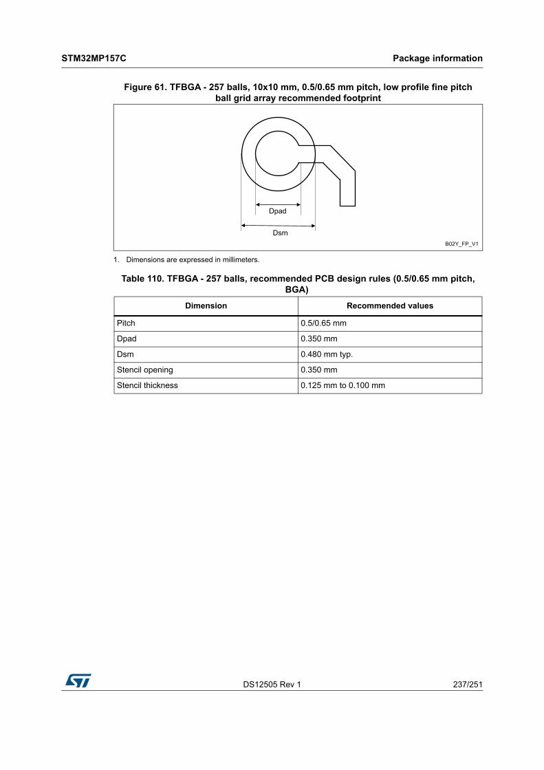
DS12505 Rev 1 237/251
STM32MP157C Package information
248
Figure 61. TFBGA - 257 balls, 10x10 mm, 0.5/0.65 mm pitch, low profile fine pitchball grid array recommended footprint
1. Dimensions are expressed in millimeters.
Table 110. TFBGA - 257 balls, recommended PCB design rules (0.5/0.65 mm pitch, BGA)
Dimension Recommended values
Pitch 0.5/0.65 mm
Dpad 0.350 mm
Dsm 0.480 mm typ.
Stencil opening 0.350 mm
Stencil thickness 0.125 mm to 0.100 mm
B02Y_FP_V1
Dpad
Dsm
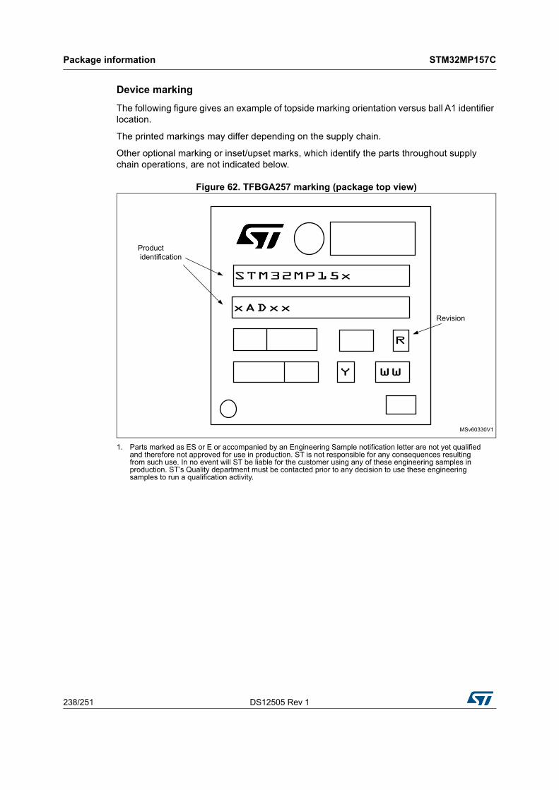
Package information STM32MP157C
238/251 DS12505 Rev 1
Device marking
The following figure gives an example of topside marking orientation versus ball A1 identifier location.
The printed markings may differ depending on the supply chain.
Other optional marking or inset/upset marks, which identify the parts throughout supply chain operations, are not indicated below.
Figure 62. TFBGA257 marking (package top view)
1. Parts marked as ES or E or accompanied by an Engineering Sample notification letter are not yet qualified and therefore not approved for use in production. ST is not responsible for any consequences resulting from such use. In no event will ST be liable for the customer using any of these engineering samples in production. ST’s Quality department must be contacted prior to any decision to use these engineering samples to run a qualification activity.
MSv60330V1
xADxx
Y WW
Product identification
R
STM32MP15x
Revision
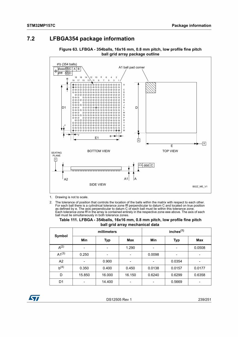
DS12505 Rev 1 239/251
STM32MP157C Package information
248
7.2 LFBGA354 package information
Figure 63. LFBGA - 354balls, 16x16 mm, 0.8 mm pitch, low profile fine pitchball grid array package outline
1. Drawing is not to scale.
2. The tolerance of position that controls the location of the balls within the matrix with respect to each other. For each ball there is a cylindrical tolerance zone fff perpendicular to datum C and located on true position as defined by e. The axis perpendicular to datum C of each ball must lie within this tolerance zone. Each tolerance zone fff in the array is contained entirely in the respective zone eee above. The axis of each ball must lie simultaneously in both tolerance zones.
Table 111. LFBGA - 354balls, 16x16 mm, 0.8 mm pitch, low profile fine pitchball grid array mechanical data
Symbolmillimeters inches(1)
Min Typ Max Min Typ Max
A(2) - - 1.290 - - 0.0508
A1(3) 0.250 - - 0.0098 - -
A2 - 0.900 - - 0.0354 -
b(4) 0.350 0.400 0.450 0.0138 0.0157 0.0177
D 15.850 16.000 16.150 0.6240 0.6299 0.6358
D1 - 14.400 - - 0.5669 -
K
H
D
A
C
EFG
J
LMNPR
UT
VW
B02Z_ME_V1
12
34
56
78
910
1112
15 131416
1718
19
D1
E1
F
F
e
e
b (354 balls)eee M C A Bfff M C
A1 ball pad corner
B
D
E
A
A1
C
SEATING PLANE
A
BOTTOM VIEW TOP VIEW
SIDE VIEW
ddd C
A2

Package information STM32MP157C
240/251 DS12505 Rev 1
Figure 64. LFBGA - 354balls, 16x16 mm, 0.8 mm pitch, low profile fine pitchball grid array recommended footprint
1. Dimensions are expressed in millimeters.
E 15.850 16.000 16.150 0.6240 0.6299 0.6358
E1 - 14.400 - - 0.5669 -
e - 0.800 - - 0.0315 -
F - 0.800 - - 0.0315 -
ddd - - 0.100 - - 0.0039
eee(5) - - 0.150 - - 0.0059
fff(6) - - 0.080 - - 0.0031
1. Values in inches are converted from mm and rounded to 4 decimal digits.
2. LFBGA stands for Low profile Fine pitch Ball Grid Array package. Low profile: 1.20mm < A ≤ 1.70mm / Fine pitch: e < 1.00mm pitch. The total profile height (Dim A) is measured from the seating plane to the top of the component The maximum total package height is calculated by the RSS method (Root Sum Square). A Max = A1 Typ + A2 Typ + A4 Typ + √(A1² + A2² + A4² tolerance values).
3. The terminal A1 corner must be identified on the top surface by using a corner chamfer, ink or metalized markings, or other feature of package body or integral heat slug. A distinguishing feature is allowable on the bottom surface of the package to identify the terminal A1 corner. Exact shape of each corner is optional.
4. Initial ball equal 0.400 mm.
5. The tolerance of position that controls the location of the pattern of balls with respect to datums A and B. For each ball there is a cylindrical tolerance zone eee perpendicular to datum C and located on true position with respect to datums A and B as defined by e. The axis perpendicular to datum C of each ball must lie within this tolerance zone.
6. The tolerance of position that controls the location of the balls within the matrix with respect to each other. For each ball there is a cylindrical tolerance zone fff perpendicular to datum C and located on true position as defined by e. The axis perpendicular to datum C of each ball must lie within this tolerance zone. Each tolerance zone fff in the array is contained entirely in the respective zone eee above The axis of each ball must lie simultaneously in both tolerance zones.
Table 111. LFBGA - 354balls, 16x16 mm, 0.8 mm pitch, low profile fine pitchball grid array mechanical data (continued)
Symbolmillimeters inches(1)
Min Typ Max Min Typ Max
B02Z_FP_V1
Dpad
Dsm

DS12505 Rev 1 241/251
STM32MP157C Package information
248
Device marking
The following figure gives an example of topside marking orientation versus ball A1 identifier location.
The printed markings may differ depending on the supply chain.
Other optional marking or inset/upset marks, which identify the parts throughout supply chain operations, are not indicated below.
Figure 65. LFBGA354 marking (package top view)
1. Parts marked as ES or E or accompanied by an Engineering Sample notification letter are not yet qualified and therefore not approved for use in production. ST is not responsible for any consequences resulting from such use. In no event will ST be liable for the customer using any of these engineering samples in production. ST’s Quality department must be contacted prior to any decision to use these engineering samples to run a qualification activity.
Table 112. LFBGA - 354 balls, recommended PCB design rules (0.8 mm pitch, BGA)
Dimension Recommended values
Pitch 0.8 mm
Dpad 0.400 mm
Dsm0.550 mm typ. (depends on the soldermask registration tolerance)
Stencil opening 0.400 mm
Stencil thickness 0.125 mm to 0.100 mm
MSv60332V1
Y WW
Product identification
R
STM32MP15xxABx
Revision
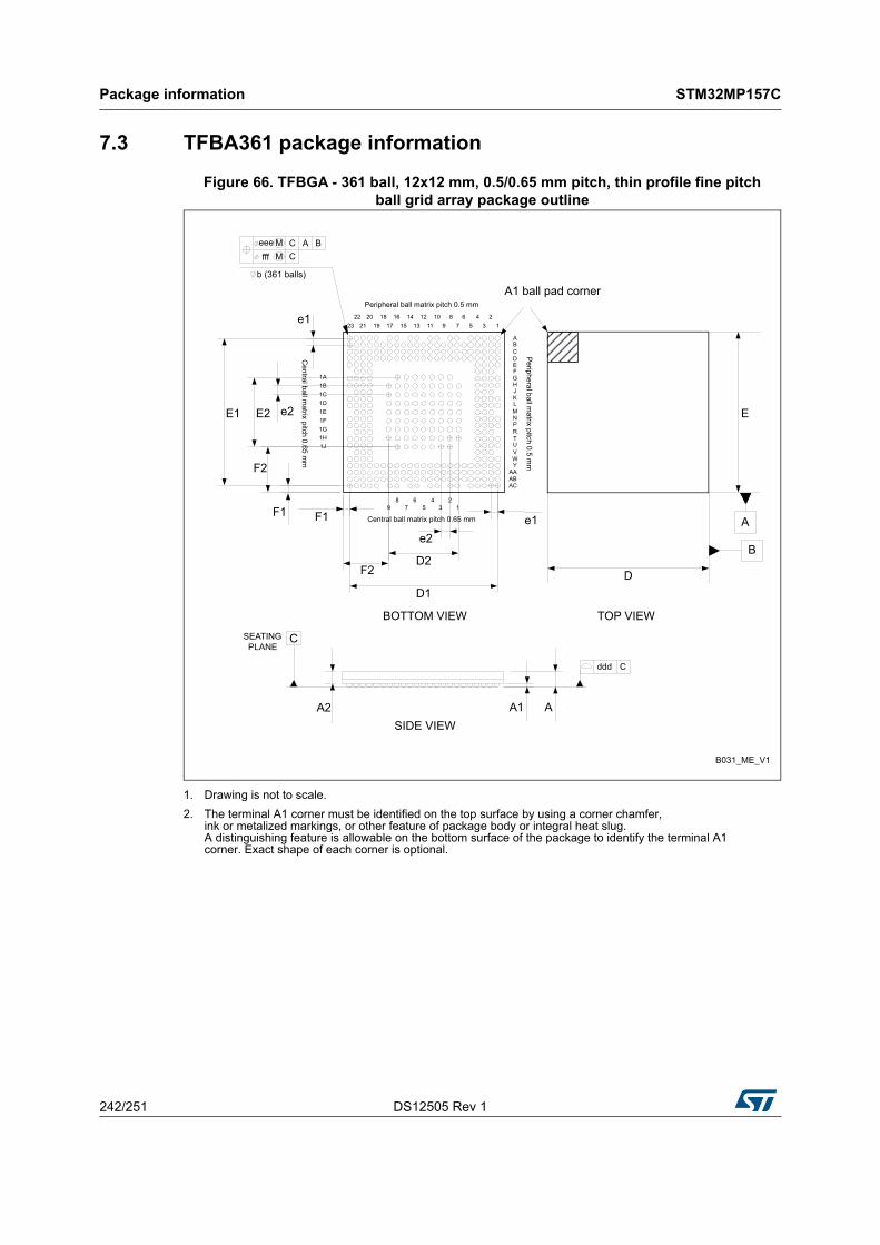
Package information STM32MP157C
242/251 DS12505 Rev 1
7.3 TFBA361 package information
Figure 66. TFBGA - 361 ball, 12x12 mm, 0.5/0.65 mm pitch, thin profile fine pitchball grid array package outline
1. Drawing is not to scale.
2. The terminal A1 corner must be identified on the top surface by using a corner chamfer, ink or metalized markings, or other feature of package body or integral heat slug. A distinguishing feature is allowable on the bottom surface of the package to identify the terminal A1 corner. Exact shape of each corner is optional.
B031_ME_V1
e2
12
34
56
78
9
e1
ABAC
YAA
WVUTRPNMLKJHGFEDCBA
Peripheral ball m
atrix pitch 0.5 mm
Central ball matrix pitch 0.65 mm
Peripheral ball matrix pitch 0.5 mm
D2
D1DF2
F1F1
F2
Central ball m
atrix pitch 0.65 mm
1J1H1G1F1E1D1C1B1A
e2E2E1 E
B
e1
A1 ball pad corner
12
34
56
78
910
1112
1314
1516
1718
1920
2122
23
BOTTOM VIEW
C A BCM
Meeefff
b (361 balls)
A2
SEATINGPLANE
C
A1 A
ddd C
A
TOP VIEW
SIDE VIEW

DS12505 Rev 1 243/251
STM32MP157C Package information
248
Table 113. TFBGA - 361 ball, 12x12 mm, 0.5/0.65 mm pitch, thin profile fine pitchball grid array mechanical data
Symbolmillimeters inches(1)
1. Values in inches are converted from mm and rounded to 4 decimal digits.
Min Typ Max Min Typ Max
A(2)
2. TFBGA stands for Thin Profile Fine Pitch Ball Grid Array. The total profile height (dim A) is measured from the seating plane to the top of the component.
- - 1.200 - - 0.0472
A1 0.150 - - 0.0059 - -
A2 - 0.810 - - 0.0319 -
b(3)
3. Initial ball equal to 0.300 mm.
0.300 0.350 0.400 0.0118 0.0138 0.0157
D 11.850 12.000 12.150 0.4665 0.4724 0.4783
D1 - 11.000 - - 0.4331 -
E 11.850 12.000 12.150 0.4665 0.4724 0.4783
E1 - 11.000 - - 0.4331 -
D2 - 5.200 - - 0.2047 -
E2 - 5.200 - - 0.2047 -
e1 - 0.500 - - 0.0197 -
e2 - 0.650 - - 0.0256 -
F1 - 0.500 - - 0.0197 -
F2 - 3.400 - - 0.1339 -
ddd - - 0.080 - - 0.0031
eee(4)
4. The tolerance of position that controls the location of the pattern of balls with respect to datums A and B. For each ball there is a cylindrical tolerance zone eee perpendicular to datum C and located on true position with respect to datums A and B as defined by e. The axis perpendicular to datum C of each ball must lie within this tolerance zone.
- - 0.150 - - 0.0059
fff(5)
5. The tolerance of position that controls the location of the balls within the matrix with respect to each other. For each ball there is a cylindrical tolerance zone fff perpendicular to datum C and located on true position as defined by e. The axis perpendicular to datum C of each ball must lie within this tolerance zone. Each tolerance zone fff in the array is contained entirely in the respective zone eee above The axis of each ball must lie simultaneously in both tolerance zones.
- - 0.080 - - 0.0031

Package information STM32MP157C
244/251 DS12505 Rev 1
Figure 67. TFBGA - 361 ball, 12x12 mm, 0.5/0.65 mm pitch, thin profile fine pitchball grid array recommended footprint
Table 114. TFBGA - 361 ball, recommended PCB design rules (0.5/0.65 mm pitch BGA)
Dimension Recommended values
Pitch 0.5/0.65 mm
Dpad 0.350 mm
Dsm 0.480 mm typ.
Stencil opening 0.350 mm
Stencil thickness 0.125 mm to 0.100 mm
B031_FP_V2
Dpad
Dsm

DS12505 Rev 1 245/251
STM32MP157C Package information
248
Device marking
The following figure gives an example of topside marking orientation versus ball A1 identifier location.
The printed markings may differ depending on the supply chain.
Other optional marking or inset/upset marks, which identify the parts throughout supply chain operations, are not indicated below.
Figure 68. TFBGA361 marking (package top view)
1. Parts marked as ES or E or accompanied by an Engineering Sample notification letter are not yet qualified and therefore not approved for use in production. ST is not responsible for any consequences resulting from such use. In no event will ST be liable for the customer using any of these engineering samples in production. ST’s Quality department must be contacted prior to any decision to use these engineering samples to run a qualification activity.
MSv60331V1
xACxx
Y WW
Product identification
R
STM32MP15x
Revision

Package information STM32MP157C
246/251 DS12505 Rev 1
7.4 LFBGA448 package information
Figure 69. LFBGA - 448 balls, 18x18 mm, 0.8 mm pitch, low profile fine pitch ballgrid array package outline
1. Drawing is not to scale.
2. The tolerance of position that controls the location of the balls within the matrix with respect to each other. For each ball there is a cylindrical tolerance zone fff perpendicular to datum C and located on true position as defined by e. The axis perpendicular to datum C of each ball must lie within this tolerance zone. Each tolerance zone fff in the array is contained entirely in the respective zone eee above. The axis of each ball must lie simultaneously in both tolerance zones.
Table 115. LFBGA - 448 balls, 18x18 mm, 0.8 mm pitch, low profile fine pitch ballgrid array mechanical data
Symbolmillimeters inches(1)
Min Typ Max Min Typ Max
A - - 1.270 - - 0.0500
A1 0.250 0.290 0.330 0.0098 0.0114 0.0130
A2 0.790 0.880 0.970 0.0311 0.0346 0.0382
A3 0.240 0.28 0.320 0.0094 0.0110 0.0126
A4 0.550 0.600 0.650 0.0217 0.0236 0.0256
b(2) 0.350 0.400 0.450 0.0138 0.0157 0.0177
B032_LFBGA448_ME_V1
K
H
D
ABC
EFG
J
LMNPR
UT
VWYAAAB
A
12
34
56
78
910
1112
15 131416
1718
1920
2122
D
E
F
B
E1F
D1
e
e
A1 corner index area
b (448 Balls)
eee C A BCfff
A4 A3
A2 A
A1
C
Cdd
d
SEATING PLANE
BOTTOM VIEW TOP VIEW
SIDE VIEW

DS12505 Rev 1 247/251
STM32MP157C Package information
248
Figure 70. LFBGA - 448 balls, 18x18 mm, 0.8 mm pitch, low profile fine pitch ballgrid array recommended footprint
1. Dimensions are expressed in millimeters.
D 17.900 18.000 18.100 0.7047 0.7087 0.7126
D1 - 16.800 - - 0.6614 -
E 17.900 18.000 18.100 0.7047 0.7087 0.7126
E1 - 16.800 - - 0.6614 -
e - 0.800 - - 0.0315 -
F - 0.600 - - 0.0236 -
ddd - 0.120 - - 0.0047 -
eee(3) - 0.150 - - 0.0059 -
fff(4) - 0.080 - - 0.0031 -
1. Values in inches are converted from mm and rounded to 4 decimal digits.
2. Low profile: 1.20 mm < A ≤ 1.70 mm / Fine pitch: e < 1.00 mm pitch. The total profile height (Dim.A) is measured from the seating plane “C” to the top of the component. The maximum total package height is calculated by the RSS method (Root Sum Square). A Max = A1 Typ + A2 Typ + A4 Typ + √(A1² + A2² + A4² tolerance values).
3. The typical ball diameter before mounting is 0.40 mm
4. The tolerance of position that controls the location of the pattern of balls with respect to datums A and B. For each ball there is a cylindrical tolerance zone eee perpendicular to datum C and located on true position with respect to datums A and B as defined by e. The axis perpendicular to datum C of each ball must lie within this tolerance zone.
Table 116. LFBGA - 448 balls, recommended PCB design rules (0.8 mm pitch, BGA)
Dimension Recommended values
Pitch 0.8 mm
Dpad 0.400 mm
Table 115. LFBGA - 448 balls, 18x18 mm, 0.8 mm pitch, low profile fine pitch ballgrid array mechanical data (continued)
Symbolmillimeters inches(1)
Min Typ Max Min Typ Max
B032_LFBGA448_FP_V1
Dpad
Dsm
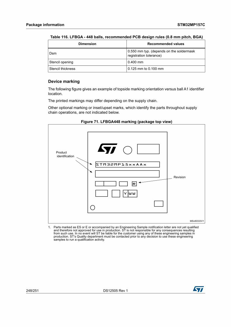
Package information STM32MP157C
248/251 DS12505 Rev 1
Device marking
The following figure gives an example of topside marking orientation versus ball A1 identifier location.
The printed markings may differ depending on the supply chain.
Other optional marking or inset/upset marks, which identify the parts throughout supply chain operations, are not indicated below.
Figure 71. LFBGA448 marking (package top view)
1. Parts marked as ES or E or accompanied by an Engineering Sample notification letter are not yet qualified and therefore not approved for use in production. ST is not responsible for any consequences resulting from such use. In no event will ST be liable for the customer using any of these engineering samples in production. ST’s Quality department must be contacted prior to any decision to use these engineering samples to run a qualification activity.
Dsm0.550 mm typ. (depends on the soldermask registration tolerance)
Stencil opening 0.400 mm
Stencil thickness 0.125 mm to 0.100 mm
Table 116. LFBGA - 448 balls, recommended PCB design rules (0.8 mm pitch, BGA)
Dimension Recommended values
MSv60333V1
Y WW
Product identification
STM32MP15xxAAx
R
Revision

DS12505 Rev 1 249/251
STM32MP157C Ordering information
249
8 Ordering information
For a list of available options (speed, package, etc.) or for further information on any aspect of this device, please contact your nearest ST sales office.
Table 117. STM32MP157C ordering information scheme
Example: STM32 MP 157 C AA 3 T
Device family
STM32 = Arm-based 32-bit processor
Product type
MP = MPU product
Device subfamily
157 = STM32MP157 Line
Security option
C = Secure boot and cryptography hardware
Package and pin count
AD = TFBGA257 10x10, 257 balls pitch 0.5 mm
AB = LFBGA354 16x16, 354 balls pitch 0.8 mm
AC = TFBGA361 12x12, 361 balls pitch 0.5 mm
AA = LFBGA448 18x18, 448 balls pitch 0.8 mm
Junction temperature range
3 = -40°C < TJ < +125°C
Packing
T = tape and reel
No character = tray or tube
Revision history STM32MP157C
250/251 DS12505 Rev 1
9 Revision history
Table 118. Document revision history
Date Revision Changes
07-Feb-2019 1 Initial release.

DS12505 Rev 1 251/251
STM32MP157C
251
IMPORTANT NOTICE – PLEASE READ CAREFULLY
STMicroelectronics NV and its subsidiaries (“ST”) reserve the right to make changes, corrections, enhancements, modifications, and improvements to ST products and/or to this document at any time without notice. Purchasers should obtain the latest relevant information on ST products before placing orders. ST products are sold pursuant to ST’s terms and conditions of sale in place at the time of order acknowledgement.
Purchasers are solely responsible for the choice, selection, and use of ST products and ST assumes no liability for application assistance or the design of Purchasers’ products.
No license, express or implied, to any intellectual property right is granted by ST herein.
Resale of ST products with provisions different from the information set forth herein shall void any warranty granted by ST for such product.
ST and the ST logo are trademarks of ST. All other product or service names are the property of their respective owners.
Information in this document supersedes and replaces information previously supplied in any prior versions of this document.
© 2019 STMicroelectronics – All rights reserved