datasheet - ld39200 - 2 a high psrr ultra low drop linear ... · cin r1 r2 cout l d39200 byp...
TRANSCRIPT

Features• Input voltage from 1.25 V to 6.0 V• Ultra low drop: 130 mV (typ.) at 2 A load• 1 % output accuracy at 25 °C, 2 % in full temperature range• High PSRR: 70 dB at 1 kHz• Reverse current protection• 2 A guaranteed output current• Available in fixed and adjustable output voltage version from 0.5 V with 100 mV
step• Power Good• Internal current and thermal limit• Operating junction temperature range: -40 °C to 125 °C• DFN6 (3 x 3 mm) and DFN8 (4 x 4 mm) packages
Applications• Telecom infrastructure• Medium power POL
DescriptionThe LD39200 provides 2 A of maximum current with an input voltage range from 1.25V to 6.0 V, and a typical dropout voltage of 130 mV.
It is stable with ceramic capacitors on the output (10 µF).
Typical power supply rejection ratio is 70 dB at 1 kHz and starts to roll off at 20 kHz.
The enable logic control function puts the LD39200 in shutdown mode, reducing thetotal current consumption to 10 nA (typ.).
Power Good flag is available on a dedicated pin.
The device also includes reverse current protection, short-circuit constant currentlimit and thermal protection.
Typical applications are for Telecom infrastructure and consumer.
Maturity status link
LD39200
2 A high PSRR ultra low drop linear regulator with reverse current protection
LD39200
Datasheet
DS10079 - Rev 3 - September 2018For further information contact your local STMicroelectronics sales office.
www.st.com

1 Block diagram
Figure 1. Block diagram
VIN
VOUT
500mV
PMOS
OPAMPVFB
Bandgap reference
R3
R4
RC filter
R2
R1
VREF
VFBPG
EN
Power good
EnableInternal enable
Reverse current
protection500mV
AM13907V1
LD39200Block diagram
DS10079 - Rev 3 page 2/29

2 Pin configuration and description
Figure 2. Pin configuration (top view)
AM13909V1
IN
IN
EN
PG
OUT
OUT
ADJ/SENSE
GND
OUT
ADJ/SENSE
GND
IN
EN
PG
Table 1. DFN6 (3 x 3 mm) package pin description
Pin name Pin number Description
IN 6 Input voltage
GND 3 Ground
EN 5 Enable pin. The device is in OFF state when this pin is pulled low
ADJ/sense (1) 2Adjustable pin on ADJ version can be connected to external resistor divider to set the outputvoltage.
Output sense pin on the fixed version has to be connected to VOUT
OUT 1 Output voltage
PG 4 Power Good
GND Exposed pad Exposed pad should be connected to GND
1. The output sense pin of the fixed version has to be connected to the output pin for proper operation.
Table 2. DFN8 (4 x 4 mm) package pin description
Pin name Pin number Description
IN (1) 7, 8 Input voltage
GND 4 Ground
EN 6 Enable pin. The device is in OFF state when this pin is pulled low
ADJ/sense (2) 3Adjustable pin on ADJ version can be connected to external resistor divider to set the outputvoltage.
Output sense pin on the fixed version has to be connected to VOUT
OUT (3) 1, 2 Output voltage
PG 5 Power Good
GND Exposed pad Exposed pad should be connected to GND
1. Both of input pins have to be connected together on the board.2. The output sense pin of the fixed version has to be connected to the OUT pin for proper operation.3. Both of output pins have to be connected together on the board.
LD39200Pin configuration and description
DS10079 - Rev 3 page 3/29

3 Typical application
Figure 3. LD39200 typical application schematic
Adjustable version Fixed version
AM13909V1
OUT
GND
IN
EN ADJ
ON
OFF
CIN R1
R2
COUTLD39200 CBYP
(optional)
OUT
GND
IN
EN SENSE
ON
OFF
CIN
LD39200 COUT
PG PG
Note: R1 and R2 are calculated according to the following formula: R1 = R2 x (VOUT / VADJ - 1). Recommended valuefor CIN and COUT is 10 μF.
LD39200Typical application
DS10079 - Rev 3 page 4/29
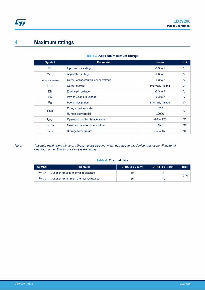
4 Maximum ratings
Table 3. Absolute maximum ratings
Symbol Parameter Value Unit
VIN Input supply voltage -0.3 to 7 V
VADJ Adjustable voltage -0.3 to 2 V
VOUT /VSENSE Output voltage/output sense voltage -0.3 to 7 V
IOUT Output current Internally limited A
EN Enable pin voltage -0.3 to 7 V
PG Power Good pin voltage -0.3 to 7 V
PD Power dissipation Internally limited W
ESDCharge device model ±500
VHuman body model ±2000
TJ-OP Operating junction temperature -40 to 125 °C
TJ-MAX Maximum junction temperature 150 °C
TSTG Storage temperature -55 to 150 °C
Note: Absolute maximum ratings are those values beyond which damage to the device may occur. Functionaloperation under these conditions is not implied.
Table 4. Thermal data
Symbol Parameter DFN6 (3 x 3 mm) DFN8 (4 x 4 mm) Unit
RTHJC Junction-to-case thermal resistance 10 4°C/W
RTHJA Junction-to- ambient thermal resistance 55 40
LD39200Maximum ratings
DS10079 - Rev 3 page 5/29

5 Electrical characteristics
(TJ = 25 °C, VIN = VOUT+1 V; VOUT = VADJ; CIN = 10 µF; COUT = 10 µF; IOUT = 10 mA; VEN = VIN)
Table 5. Electrical characteristics, adjustable version
Symbol Parameter Test conditions Min. Typ. Max. Unit
VINOperating input voltagerange 1.25 6.0 V
VADJ
Adjustable pin voltage 0.5 V
Adjustable pin voltageaccuracy
TJ = 25 °C -1.0 1.0%
-40 °C < TJ < 125 °C -2.0 2.0
IADJ Adjustable pin current -40 °C < TJ < 125 °C 100 nA
∆VADJ%/∆VIN
Static line regulationVOUT + 1 V < VIN < 6.0 V; TJ = 25 °C 0.01
%/V-40 °C < TJ < 125 °C 0.2
∆VADJ%/∆IOUT
Static load regulation0 mA < IOUT < 2 A; TJ = 25 °C 0.1
%/A-40 °C < TJ < 125 °C 0.4
VDROP Dropout voltage (1)
VIN = 1.4 V; IOUT = 1 A;
-40 °C < TJ < 125 °C120 250
mVVIN = 2.5 V; IOUT = 2 A;
-40 °C < TJ < 125 °C135 250
VIN = 5.3 V; IOUT = 2 A;
-40 °C < TJ < 125 °C110 250
eN Output noise voltageVOUT = VADJ ;
f = 10 Hz to 100 kHz45
µVRMS /VOUT
eN Output noise voltage
VIN = VOUT + 0.4 V, IOUT = 700 mA;CIN = COUT = 10 µF, R2 = 10 kΩ,
R1 = (VOUT – 0.5) x 20 kΩ,
Cbyp = 470 nF
24 µVRMS
SVR Supply voltage rejection
VOUT = 1.8 V; VIN = VOUT+0.5 V;
COUT = 10 µF; IOUT = 10 mA;
TJ = 25 °C; f = 1 kHz
70
dBVOUT = 1.8 V; VIN = VOUT + 0.5 V;
COUT = 10 µF; IOUT = 10 mA;
TJ = 25 °C; f = 100 kHz
50
VOUT = 1.8 V; VIN = VOUT + 0.5 V;
COUT = 10 µF; IOUT = 10 mA;
TJ = 25 °C; f = 500 kHz
50
dBVOUT = 1.8 V; VIN = VOUT + 0.5 V;
COUT = 10 µF; IOUT = 10 mA;
TJ = 25 °C; f = 1 MHz
40
LD39200Electrical characteristics
DS10079 - Rev 3 page 6/29

Symbol Parameter Test conditions Min. Typ. Max. Unit
IQQuiescent current
IOUT = 0 A 100 µA
IOUT = 0 A; -40 °C < TJ < 125 °C 300
IOUT = 2 A; 1 mA
IOUT = 2 A; -40 °C < TJ < 125 °C 3
Shutdown current Ven = 0, Vin = 6 V 10 nA
ISC Short-circuit current VOUT = 0 V 3.5 A
IMIN Minimum output current 0 A
VENEnable input logic low 1.25 V < VIN < 6.0 V
-40 °C < TJ < 125 °C
0.5V
Enable input logic high 1.2
IEN Enable pin input current VEN = VIN; 1.25 < VIN < 6.0 V 10 nA
PG
Power Good outputthreshold
Rising edge 0.92* Vout
VFalling edge 0.8*Vout
Power Good output voltagelow Isink = 6 mA open drain output 0.4
TSHDNThermal shutdown 170
°CHysteresis 20
1. Dropout voltage is the input-to-output voltage difference at which the output voltage is 100 mV below its nominal value; thisspecification does not apply to nominal output voltages below 1.2 V.
(TJ = 25 °C, VIN = VOUT+1 V; CIN = 10 µF; COUT = 10 µF; IOUT = 10 mA; VEN = VIN)
Table 6. Electrical characteristics, fixed version
Symbol Parameter Test conditions Min. Typ. Max. Unit
VIN Operating input voltage range 1.25 6.0 V
VOUT Output voltage accuracyTJ = 25 °C -1.0 1.0
%-40 °C < TJ < 125 °C -2.0 2.0
∆VADJ%/∆VIN
Static line regulation
VOUT + 1 V < VIN < 6.0 V;
TJ = 25 °C0.01
%/V
-40 °C < TJ < 125 °C 0.1
∆VADJ%/∆IOUT
Static load regulation0 mA < IOUT < 2 A; TJ = 25 °C 0.05
%/A-40 °C < TJ < 125 °C 0.4
VDROP Dropout voltageVOUT = 3.3 V; IOUT = 2 A;
-40 °C < TJ < 125 °C130 250 mV
eN Output noise voltage VOUT = 2.5 V; f = 10 Hz to 100 kHz 40µVRMS/VOUT
LD39200Electrical characteristics
DS10079 - Rev 3 page 7/29

Symbol Parameter Test conditions Min. Typ. Max. Unit
SVR Supply voltage rejection
VOUT = 1.8 V; VIN = VOUT + 0.5 V;
COUT = 10 µF; IOUT = 10 mA;
TJ = 25 °C; f = 1 kHz
70
dB
VOUT = 1.8 V; VIN = VOUT + 0.5 V;
COUT = 10 µF; IOUT = 10 mA;
TJ = 25 °C; f = 100 kHz
50
VOUT = 1.8 V; VIN = VOUT + 0.5 V;
COUT = 10 µF; IOUT = 10 mA;
TJ = 25 °C; f = 500 kHz
50
VOUT = 1.8 V; VIN = VOUT + 0.5 V;
COUT = 10 µF; IOUT = 10 mA;
TJ = 25 °C; f = 1 MHz
40
IQQuiescent current
IOUT = 0 A 100 µA
IOUT = 0 A; -40 °C < TJ < 125 °C 300
IOUT = 2 A; 1 mA
IOUT = 2 A; -40 °C < TJ < 125 °C 3
Shutdown current Ven = 0, Vin = 6 V 50 nA
ISC Short-circuit current VOUT = 0 V 3.5 A
IMIN Minimum output current 0 A
VENEnable input logic low 1.25 V < VIN < 6.0 V
-40 °C < TJ < 125 °C
0.5V
Enable input logic high 1.2
IEN Enable pin input current VEN = VIN; 1.25 < VIN < 6.0 V 10 nA
PGPower Good output threshold
Rising edge 0.92*VOUT
VFalling edge 0.8*VOUT
Power Good output voltagelow Isink = 6 mA open drain output 0.4
TSHDNThermal shutdown 170
°CHysteresis 20
LD39200Electrical characteristics
DS10079 - Rev 3 page 8/29
6 Application information
6.1 Thermal and short-circuit protectionsThe LD39200 is self-protected from short-circuit conditions and overtemperature. When the output load is higherthan the one supported by the device, the output current rises until the limit of typically 3.5 A is reached; at thispoint the current is kept constant even when the load impedance is zero. The thermal protection acts when thejunction temperature reaches 170 °C. The IC enters the shutdown status. As soon as the junction temperaturefalls again below 150 °C the device starts working again. In order to calculate the maximum power the device candissipate, keeping the junction temperature below TJ-OP , the following formula is used:PDMAX = 125− TAMB / RTHJ − A (1)
6.2 Output voltage setting for ADJ versionIn the adjustable version, the output voltage can be set from 0.5 V up to the input voltage minus the voltage dropacross the pass transistor (dropout voltage), by connecting a resistor divider between the ADJ pin and the output,allowing remote voltage sensing. The resistor divider can be selected using the following equation:VOUT = VADJ 1 + R1/ R2 , witℎ VADJ = 0.5 V typ. (2)
6.3 Enable pinThe LD39200 features an enable function. When the EN voltage is higher than 1.2 V the device is ON, and if it islower than 0.5 V the device is OFF. In shutdown mode, the total current consumption is 10 nA (typ). The EN pindoes not have an internal pull-up, therefore it cannot be left floating if it is not used.
6.4 Power Good pin (PG)Some applications require a flag showing that the output voltage is in the correct range. Power Good thresholddepends on the output voltage. When the output voltage is higher than 0.92 * VOUT(nom), the PG pin goes to highimpedance. If the output voltage is below 0.80 * VOUT(nom) the PG pin goes to low impedance. If the device workswell, the PG pin is at high impedance.
6.5 Reverse current protectionThe device avoids the reverse current to flow from the output to the input during any operating condition (EN = 0or EN = 1, VIN > VOUT + VDROP). During fast turn-on/off this function prevents a big current from flowing to theinput. Moreover it is used to avoid the reverse current to flow from the output pin to the input one, when otherpower supplies, providing a voltage higher than the input voltage, are connected to the output pin. If a powersupply, providing a voltage lower than LDO output voltage, is connected to OUT pin, LDO works in currentprotection, causing high power dissipation inside the device.When the device is disabled (EN = low) and VOUT > 0 V, a small current (few µA) is sunk from the OUT pin.
LD39200Application information
DS10079 - Rev 3 page 9/29

7 Typical performance characteristics
(The following plots are referred to the typical application circuit and, unless otherwise noted, at TA = 25 °C)
Figure 4. Dropout voltage vs. temperature(Vin = 1.3 V, Iout = 1 A)
0
50
100
150
200
250
-40 -25 0 25 55 85 125
mV
Temperature ºCAM13910V1
Figure 5. Dropout voltage vs. temperature(Vin = 1.4 V, Iout = 1 A)
AM13911V1
0
50
100
150
200
250
-40 -25 0 25 55 85 125
mV
Temperature ºC
Figure 6. Dropout voltage vs. temperature(Vin = 1.4 V, Iout = 2 A)
AM13912V1
0
50
100
150
200
250
300
350
400
450
500
-40 -25 0 25 55 85 125
mV
Temperature ºC
Figure 7. Dropout voltage vs. temperature(Vin = 1.5 V, Iout = 1 A)
AM13913V1
0
50
100
150
200
250
-40 -25 0 25 55 85 125
mV
Temperature ºC
LD39200Typical performance characteristics
DS10079 - Rev 3 page 10/29

Figure 8. Dropout voltage vs. temperature(Vin = 1.5 V, Iout = 2 A)
AM13914V1
0
50
100
150
200
250
300
350
400
450
500
-40 -25 0 25 55 85 125
mV
Temperature ºC
Figure 9. Dropout voltage vs. temperature(Vin = 2.5 V, Iout = 1 A)
AM13915V1
0
20
40
60
80
100
120
140
-40 -25 0 25 55 85 125
mV
Temperature ºC
Figure 10. Dropout voltage vs. temperature(Vin = 2.5 V, Iout = 2 A)
AM13916V1
0
50
100
150
200
250
300
-40 -25 0 25 55 85 125
mV
Temperature ºC
Figure 11. Reference voltage vs. temperature(Vin = 1.5 V, Iout = 10 mA)
AM13917V1
0.45
0.47
0.49
0.51
0.53
0.55
-40 -25 0 25 55 85 125
Vadj
[V]
Temperature ºC
Figure 12. Quiescent current vs. temperature(Vin = 1.5 V, Iout = 0 mA)
AM13918V1
0
0.05
0.1
0.15
0.2
0.25
0.3
-40 -25 0 25 55 85 125
Qui
esce
nt c
urre
nt [m
A]
Temperature ºC
Figure 13. Quiescent current vs. temperature(Vin = 1.5 V, Iout = 2 A)
AM13919V1
0
0.2
0.4
0.6
0.8
1
1.2
1.4
1.6
1.8
2
-40 -25 0 25 55 85 125
Qui
esce
nt c
urre
nt [m
A]
Temperature ºC
LD39200Typical performance characteristics
DS10079 - Rev 3 page 11/29
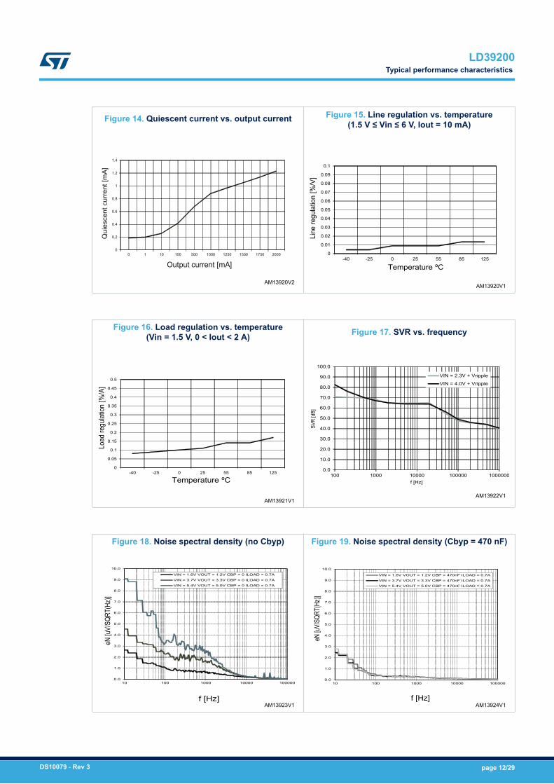
Figure 14. Quiescent current vs. output current
AM13920V2
0
0.2
0.4
0.6
0.8
1
1.2
1.4
0 1 10 100 500 1000 1250 1500 1750 2000
Qui
esce
nt c
urre
nt [m
A]
Output current [mA]
Figure 15. Line regulation vs. temperature(1.5 V ≤ Vin ≤ 6 V, Iout = 10 mA)
AM13920V1
0
0.01
0.02
0.03
0.04
0.05
0.06
0.07
0.08
0.09
0.1
-40 -25 0 25 55 85 125
Line
regu
latio
n [%
/V]
Temperature ºC
Figure 16. Load regulation vs. temperature(Vin = 1.5 V, 0 < Iout < 2 A)
AM13921V1
0
0.05
0.1
0.15
0.2
0.25
0.3
0.35
0.4
0.45
0.5
-40 -25 0 25 55 85 125
Load
regu
latio
n [%
/A]
Temperature ºC
Figure 17. SVR vs. frequency
AM13922V1
0.0
10.0
20.0
30.0
40.0
50.0
60.0
70.0
80.0
90.0
100.0
100 1000 10000 100000 1000000
SVR
[dB]
f [Hz]
VIN = 2.3V + Vripple
VIN = 4.0V + Vripple
Figure 18. Noise spectral density (no Cbyp)
AM13923V1
0.0
1.0
2.0
3.0
4.0
5.0
6.0
7.0
8.0
9.0
10.0
10 100 1000 10000 100000
eN [u
V/SQ
RT(H
z)]
f [Hz]
VIN = 1.6V VOUT = 1.2V CBP = 0 ILOAD = 0.7A
VIN = 3.7V VOUT = 3.3V CBP = 0 ILOAD = 0.7A
VIN = 5.4V VOUT = 5.0V CBP = 0 ILOAD = 0.7A
Figure 19. Noise spectral density (Cbyp = 470 nF)
AM13924V1
0.0
1.0
2.0
3.0
4.0
5.0
6.0
7.0
8.0
9.0
10.0
10 100 1000 10000 100000
eN [u
V/SQ
RT(H
z)]
f [Hz]
VIN = 1.6V VOUT = 1.2V CBP = 470nF ILOAD = 0.7A
VIN = 3.7V VOUT = 3.3V CBP = 470nF ILOAD = 0.7A
VIN = 5.4V VOUT = 5.0V CBP = 470nF ILOAD = 0.7A
LD39200Typical performance characteristics
DS10079 - Rev 3 page 12/29

Figure 20. Stability plan
AM13925V1
0.01
0.1
1
10
0 1 2 3 4 5 6 7 8 9 10 11 12 13 14 15 16 17 18 19 20 21 22 23
ES
R @
100K
Hz[
Ω]
COUT [µF] (nominal value)
STABILITY AREA
Figure 21. Enable startup, Vin = 1.25 V, Iout = 2 A
Figure 22. Enable startup, Vin = 6 V, Iout = 2 A Figure 23. Enable startup, no Cbyp
GIPG080420141550MT
VEN
VOUT
VIN = 3.7 V, VEN = from 0 to 2 V, IOUT = 100 mA, VOUT = 3.3 V, CIN = COUT = 10 µF, CBYP = 0
Figure 24. Enable startup, Cbyp = 470 nF
GIPG080420141552MT
VEN
VOUT
VIN = 3.7 V, VOUT = 3.3 V, VEN = from 0 to 2V, IOUT = 100 mA, CIN = COUT = 10 µF, CBYP = 470
Figure 25. Line transient
GIPG140420141401MT
VIN
VOUT
VIN = VEN = from 1.5 to 5.5 V, IOUT = 10 mA, NO CIN = COUT = 10 µF, TRISE = TFALL = 10 µs
LD39200Typical performance characteristics
DS10079 - Rev 3 page 13/29

Figure 26. Load transient, no Cbyp
GIPG140420141403MT
VIN
VOUT
VIN = 3.7 V, VOUT = 3.3 V, ILOAD = 10 mA to 2 A, CBYP = 0
Figure 27. Load transient, Cbyp = 470 nF
GIPG140420141405MT
VIN
VOUT
VIN = 3.7 V, VOUT = 3.3 V, ILOAD = 10 mA to 2 A, CBYP = 470 nF
LD39200Typical performance characteristics
DS10079 - Rev 3 page 14/29
8 Package mechanical data
In order to meet environmental requirements, ST offers these devices in different grades of ECOPACK®
packages, depending on their level of environmental compliance. ECOPACK® specifications, grade definitionsand product status are available at: www.st.com. ECOPACK® is an ST trademark.
LD39200Package mechanical data
DS10079 - Rev 3 page 15/29

8.1 DFN6 (3 x 3 mm) mechanical data
Figure 28. DFN6 (3 x 3 mm) package outline
7946637_C
LD39200DFN6 (3 x 3 mm) mechanical data
DS10079 - Rev 3 page 16/29

Table 7. DFN6 (3 x 3 mm) mechanical data
Dim.mm
Min. Typ. Max.
A 0.80 1
A1 0 0.02 0.05
A3 0.20
b 0.23 0.45
D 2.90 3 3.10
D2 2.23 2.50
E 2.90 3 3.10
E2 1.50 1.75
e 0.95
L 0.30 0.40 0.50
Figure 29. DFN6 (3 x 3 mm) recommended footprint (all dimensions are in mm)
7946637_C
LD39200DFN6 (3 x 3 mm) mechanical data
DS10079 - Rev 3 page 17/29

8.2 DFN6 (3 x 3 mm) tape and reel mechanical data
Figure 30. DFN6 (3 x 3 mm) tape outline
7875978_N
LD39200DFN6 (3 x 3 mm) tape and reel mechanical data
DS10079 - Rev 3 page 18/29

Figure 31. DFN6 (3 x 3 mm) reel outline
7875978_N
Table 8. DFN6 (3 x 3 mm) tape and reel mechanical data
Dim.mm
Min. Typ. Max.
A0 3.20 3.30 3.40
B0 3.20 3.30 3.40
K0 1 1.10 1.20
LD39200DFN6 (3 x 3 mm) tape and reel mechanical data
DS10079 - Rev 3 page 19/29

8.3 DFN8 (4 x 4 mm) mechanical data
Figure 32. DFN8 (4 x 4 mm) package outline
LD39200DFN8 (4 x 4 mm) mechanical data
DS10079 - Rev 3 page 20/29
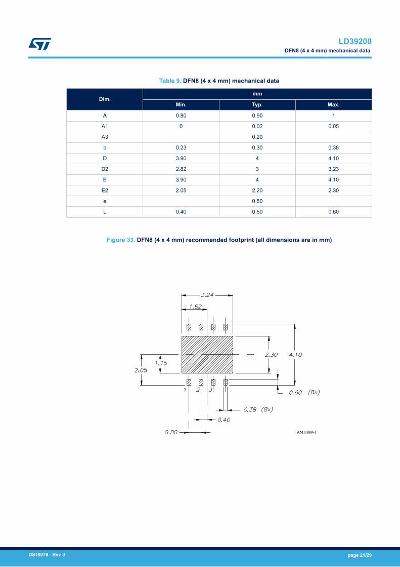
Table 9. DFN8 (4 x 4 mm) mechanical data
Dim.mm
Min. Typ. Max.
A 0.80 0.90 1
A1 0 0.02 0.05
A3 0,20
b 0.23 0.30 0.38
D 3.90 4 4.10
D2 2.82 3 3.23
E 3.90 4 4.10
E2 2.05 2.20 2.30
e 0.80
L 0.40 0.50 0.60
Figure 33. DFN8 (4 x 4 mm) recommended footprint (all dimensions are in mm)
AM11889v1
LD39200DFN8 (4 x 4 mm) mechanical data
DS10079 - Rev 3 page 21/29

8.4 DFN8 (4 x 4 mm) reel mechanical data
Figure 34. DFN8 (4 x 4 mm) tape outline (all dimensions are in mm)
7279936
LD39200DFN8 (4 x 4 mm) reel mechanical data
DS10079 - Rev 3 page 22/29

Figure 35. DFN8 (4 x 4 mm) reel outline
Table 10. DFN8 (4 x 4 mm) reel mechanical data
Dim.mm
Min. Typ. Max.
A 330
C 12.8 13.0 13.2
D 20.2
N 60
T 22.4
LD39200DFN8 (4 x 4 mm) reel mechanical data
DS10079 - Rev 3 page 23/29

9 Ordering information
Table 11. Order codes
DFN6 (3 x 3 mm) DFN8 (4 x 4 mm) Output voltage
LD39200PUR LD39200DPUR ADJ
LD39200PU33R 3.3 V
LD39200Ordering information
DS10079 - Rev 3 page 24/29
Revision history
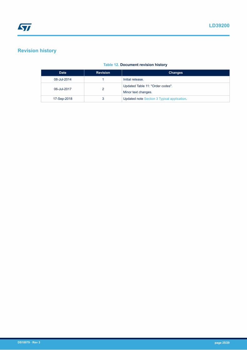
Table 12. Document revision history
Date Revision Changes
08-Jul-2014 1 Initial release.
06-Jul-2017 2Updated Table 11: "Order codes".
Minor text changes.
17-Sep-2018 3 Updated note Section 3 Typical application.
LD39200
DS10079 - Rev 3 page 25/29

Contents
1 Block diagram . . . . . . . . . . . . . . . . . . . . . . . . . . . . . . . . . . . . . . . . . . . . . . . . . . . . . . . . . . . . . . . . . . . . .2
2 Pin configuration and description. . . . . . . . . . . . . . . . . . . . . . . . . . . . . . . . . . . . . . . . . . . . . . . . . .3
3 Typical application. . . . . . . . . . . . . . . . . . . . . . . . . . . . . . . . . . . . . . . . . . . . . . . . . . . . . . . . . . . . . . . . .4
4 Maximum ratings . . . . . . . . . . . . . . . . . . . . . . . . . . . . . . . . . . . . . . . . . . . . . . . . . . . . . . . . . . . . . . . . . .5
5 Electrical characteristics. . . . . . . . . . . . . . . . . . . . . . . . . . . . . . . . . . . . . . . . . . . . . . . . . . . . . . . . . . .6
6 Application information. . . . . . . . . . . . . . . . . . . . . . . . . . . . . . . . . . . . . . . . . . . . . . . . . . . . . . . . . . . .9
6.1 Thermal and short-circuit protections . . . . . . . . . . . . . . . . . . . . . . . . . . . . . . . . . . . . . . . . . . . . . . 9
6.2 Output voltage setting for ADJ version . . . . . . . . . . . . . . . . . . . . . . . . . . . . . . . . . . . . . . . . . . . . . 9
6.3 Enable pin . . . . . . . . . . . . . . . . . . . . . . . . . . . . . . . . . . . . . . . . . . . . . . . . . . . . . . . . . . . . . . . . . . . . 9
6.4 Power Good pin (PG) . . . . . . . . . . . . . . . . . . . . . . . . . . . . . . . . . . . . . . . . . . . . . . . . . . . . . . . . . . . 9
6.5 Reverse current protection. . . . . . . . . . . . . . . . . . . . . . . . . . . . . . . . . . . . . . . . . . . . . . . . . . . . . . . 9
7 Typical performance characteristics . . . . . . . . . . . . . . . . . . . . . . . . . . . . . . . . . . . . . . . . . . . . . .10
8 Package information. . . . . . . . . . . . . . . . . . . . . . . . . . . . . . . . . . . . . . . . . . . . . . . . . . . . . . . . . . . . . .15
8.1 DFN6 (3 x 3 mm) package information. . . . . . . . . . . . . . . . . . . . . . . . . . . . . . . . . . . . . . . . . . . . 15
8.2 DFN6 (3 x 3 mm) packing information . . . . . . . . . . . . . . . . . . . . . . . . . . . . . . . . . . . . . . . . . . . . 17
8.3 DFN8 (4 x 4 mm) package information. . . . . . . . . . . . . . . . . . . . . . . . . . . . . . . . . . . . . . . . . . . . 19
8.4 DFN8 (4 x 4 mm) packing information . . . . . . . . . . . . . . . . . . . . . . . . . . . . . . . . . . . . . . . . . . . . 21
9 Ordering information . . . . . . . . . . . . . . . . . . . . . . . . . . . . . . . . . . . . . . . . . . . . . . . . . . . . . . . . . . . . .24
Revision history . . . . . . . . . . . . . . . . . . . . . . . . . . . . . . . . . . . . . . . . . . . . . . . . . . . . . . . . . . . . . . . . . . . . . . .25
LD39200Contents
DS10079 - Rev 3 page 26/29

List of tablesTable 1. DFN6 (3 x 3 mm) package pin description . . . . . . . . . . . . . . . . . . . . . . . . . . . . . . . . . . . . . . . . . . . . . . . . . . . 3Table 2. DFN8 (4 x 4 mm) package pin description . . . . . . . . . . . . . . . . . . . . . . . . . . . . . . . . . . . . . . . . . . . . . . . . . . . 3Table 3. Absolute maximum ratings . . . . . . . . . . . . . . . . . . . . . . . . . . . . . . . . . . . . . . . . . . . . . . . . . . . . . . . . . . . . . 5Table 4. Thermal data. . . . . . . . . . . . . . . . . . . . . . . . . . . . . . . . . . . . . . . . . . . . . . . . . . . . . . . . . . . . . . . . . . . . . . . 5Table 5. Electrical characteristics, adjustable version . . . . . . . . . . . . . . . . . . . . . . . . . . . . . . . . . . . . . . . . . . . . . . . . . 6Table 6. Electrical characteristics, fixed version . . . . . . . . . . . . . . . . . . . . . . . . . . . . . . . . . . . . . . . . . . . . . . . . . . . . . 7Table 7. DFN6 (3 x 3 mm) mechanical data . . . . . . . . . . . . . . . . . . . . . . . . . . . . . . . . . . . . . . . . . . . . . . . . . . . . . . . 17Table 8. DFN6 (3 x 3 mm) tape and reel mechanical data . . . . . . . . . . . . . . . . . . . . . . . . . . . . . . . . . . . . . . . . . . . . . 19Table 9. DFN8 (4 x 4 mm) mechanical data . . . . . . . . . . . . . . . . . . . . . . . . . . . . . . . . . . . . . . . . . . . . . . . . . . . . . . . 21Table 10. DFN8 (4 x 4 mm) reel mechanical data . . . . . . . . . . . . . . . . . . . . . . . . . . . . . . . . . . . . . . . . . . . . . . . . . . . . 23Table 11. Order codes . . . . . . . . . . . . . . . . . . . . . . . . . . . . . . . . . . . . . . . . . . . . . . . . . . . . . . . . . . . . . . . . . . . . . . 24Table 12. Document revision history . . . . . . . . . . . . . . . . . . . . . . . . . . . . . . . . . . . . . . . . . . . . . . . . . . . . . . . . . . . . . 25
LD39200List of tables
DS10079 - Rev 3 page 27/29

List of figuresFigure 1. Block diagram . . . . . . . . . . . . . . . . . . . . . . . . . . . . . . . . . . . . . . . . . . . . . . . . . . . . . . . . . . . . . . . . . . . . 2Figure 2. Pin configuration (top view) . . . . . . . . . . . . . . . . . . . . . . . . . . . . . . . . . . . . . . . . . . . . . . . . . . . . . . . . . . . 3Figure 3. LD39200 typical application schematic . . . . . . . . . . . . . . . . . . . . . . . . . . . . . . . . . . . . . . . . . . . . . . . . . . . 4Figure 4. Dropout voltage vs. temperature (Vin = 1.3 V, Iout = 1 A) . . . . . . . . . . . . . . . . . . . . . . . . . . . . . . . . . . . . . . 10Figure 5. Dropout voltage vs. temperature (Vin = 1.4 V, Iout = 1 A) . . . . . . . . . . . . . . . . . . . . . . . . . . . . . . . . . . . . . . 10Figure 6. Dropout voltage vs. temperature (Vin = 1.4 V, Iout = 2 A) . . . . . . . . . . . . . . . . . . . . . . . . . . . . . . . . . . . . . . 10Figure 7. Dropout voltage vs. temperature (Vin = 1.5 V, Iout = 1 A) . . . . . . . . . . . . . . . . . . . . . . . . . . . . . . . . . . . . . . 10Figure 8. Dropout voltage vs. temperature (Vin = 1.5 V, Iout = 2 A) . . . . . . . . . . . . . . . . . . . . . . . . . . . . . . . . . . . . . . 11Figure 9. Dropout voltage vs. temperature (Vin = 2.5 V, Iout = 1 A) . . . . . . . . . . . . . . . . . . . . . . . . . . . . . . . . . . . . . . 11Figure 10. Dropout voltage vs. temperature (Vin = 2.5 V, Iout = 2 A) . . . . . . . . . . . . . . . . . . . . . . . . . . . . . . . . . . . . . . 11Figure 11. Reference voltage vs. temperature (Vin = 1.5 V, Iout = 10 mA) . . . . . . . . . . . . . . . . . . . . . . . . . . . . . . . . . . 11Figure 12. Quiescent current vs. temperature (Vin = 1.5 V, Iout = 0 mA) . . . . . . . . . . . . . . . . . . . . . . . . . . . . . . . . . . . 11Figure 13. Quiescent current vs. temperature (Vin = 1.5 V, Iout = 2 A). . . . . . . . . . . . . . . . . . . . . . . . . . . . . . . . . . . . . 11Figure 14. Quiescent current vs. output current . . . . . . . . . . . . . . . . . . . . . . . . . . . . . . . . . . . . . . . . . . . . . . . . . . . . 12Figure 15. Line regulation vs. temperature (1.5 V ≤ Vin ≤ 6 V, Iout = 10 mA) . . . . . . . . . . . . . . . . . . . . . . . . . . . . . . . . 12Figure 16. Load regulation vs. temperature (Vin = 1.5 V, 0 < Iout < 2 A). . . . . . . . . . . . . . . . . . . . . . . . . . . . . . . . . . . . 12Figure 17. SVR vs. frequency . . . . . . . . . . . . . . . . . . . . . . . . . . . . . . . . . . . . . . . . . . . . . . . . . . . . . . . . . . . . . . . . 12Figure 18. Noise spectral density (no Cbyp) . . . . . . . . . . . . . . . . . . . . . . . . . . . . . . . . . . . . . . . . . . . . . . . . . . . . . . 12Figure 19. Noise spectral density (Cbyp = 470 nF) . . . . . . . . . . . . . . . . . . . . . . . . . . . . . . . . . . . . . . . . . . . . . . . . . . 12Figure 20. Stability plan . . . . . . . . . . . . . . . . . . . . . . . . . . . . . . . . . . . . . . . . . . . . . . . . . . . . . . . . . . . . . . . . . . . . 13Figure 21. Enable startup, Vin = 1.25 V, Iout = 2 A . . . . . . . . . . . . . . . . . . . . . . . . . . . . . . . . . . . . . . . . . . . . . . . . . . 13Figure 22. Enable startup, Vin = 6 V, Iout = 2 A . . . . . . . . . . . . . . . . . . . . . . . . . . . . . . . . . . . . . . . . . . . . . . . . . . . . 13Figure 23. Enable startup, no Cbyp . . . . . . . . . . . . . . . . . . . . . . . . . . . . . . . . . . . . . . . . . . . . . . . . . . . . . . . . . . . . 13Figure 24. Enable startup, Cbyp = 470 nF . . . . . . . . . . . . . . . . . . . . . . . . . . . . . . . . . . . . . . . . . . . . . . . . . . . . . . . . 13Figure 25. Line transient . . . . . . . . . . . . . . . . . . . . . . . . . . . . . . . . . . . . . . . . . . . . . . . . . . . . . . . . . . . . . . . . . . . . 13Figure 26. Load transient, no Cbyp. . . . . . . . . . . . . . . . . . . . . . . . . . . . . . . . . . . . . . . . . . . . . . . . . . . . . . . . . . . . . 14Figure 27. Load transient, Cbyp = 470 nF . . . . . . . . . . . . . . . . . . . . . . . . . . . . . . . . . . . . . . . . . . . . . . . . . . . . . . . . 14Figure 28. DFN6 (3 x 3 mm) package outline . . . . . . . . . . . . . . . . . . . . . . . . . . . . . . . . . . . . . . . . . . . . . . . . . . . . . . 16Figure 29. DFN6 (3 x 3 mm) recommended footprint (all dimensions are in mm). . . . . . . . . . . . . . . . . . . . . . . . . . . . . . 17Figure 30. DFN6 (3 x 3 mm) tape outline. . . . . . . . . . . . . . . . . . . . . . . . . . . . . . . . . . . . . . . . . . . . . . . . . . . . . . . . . 18Figure 31. DFN6 (3 x 3 mm) reel outline . . . . . . . . . . . . . . . . . . . . . . . . . . . . . . . . . . . . . . . . . . . . . . . . . . . . . . . . . 19Figure 32. DFN8 (4 x 4 mm) package outline . . . . . . . . . . . . . . . . . . . . . . . . . . . . . . . . . . . . . . . . . . . . . . . . . . . . . . 20Figure 33. DFN8 (4 x 4 mm) recommended footprint (all dimensions are in mm). . . . . . . . . . . . . . . . . . . . . . . . . . . . . . 21Figure 34. DFN8 (4 x 4 mm) tape outline (all dimensions are in mm). . . . . . . . . . . . . . . . . . . . . . . . . . . . . . . . . . . . . . 22Figure 35. DFN8 (4 x 4 mm) reel outline . . . . . . . . . . . . . . . . . . . . . . . . . . . . . . . . . . . . . . . . . . . . . . . . . . . . . . . . . 23
LD39200List of figures
DS10079 - Rev 3 page 28/29

IMPORTANT NOTICE – PLEASE READ CAREFULLY
STMicroelectronics NV and its subsidiaries (“ST”) reserve the right to make changes, corrections, enhancements, modifications, and improvements to STproducts and/or to this document at any time without notice. Purchasers should obtain the latest relevant information on ST products before placing orders. STproducts are sold pursuant to ST’s terms and conditions of sale in place at the time of order acknowledgement.
Purchasers are solely responsible for the choice, selection, and use of ST products and ST assumes no liability for application assistance or the design ofPurchasers’ products.
No license, express or implied, to any intellectual property right is granted by ST herein.
Resale of ST products with provisions different from the information set forth herein shall void any warranty granted by ST for such product.
ST and the ST logo are trademarks of ST. All other product or service names are the property of their respective owners.
Information in this document supersedes and replaces information previously supplied in any prior versions of this document.
© 2018 STMicroelectronics – All rights reserved
LD39200
DS10079 - Rev 3 page 29/29