datasheet - dlnmh9ip6v2uc.cloudfront.net · datasheet easypoint tm n35p112 navigation module...
TRANSCRIPT

Datasheet
EasyPoint TM N35P112 Navigat ion Module
1 General DescriptionEasyPoint™ N35P112 is a miniature joystick module concept based on contact-less, magnetic movement detection. The integrated two-dimensional linear encoder monitors the movement of the magnet incorporated in the knob and provides directly the x and y coordinates via I²C output. An integrated mechanical push button built in the module provides a “select” function.
Figure 1. N35P112-xxxxx-H
2 Key Features XY coordinates direct read with 8-bit resolution 2.7V to 3.6V operating voltage Down to 1.7V I/O voltage Lateral magnet movement radius up to 0.5mm High-speed I²C interface Configurable interrupt output for motion detection Push button feature
3 ApplicationsThe EasyPoint™ N35P112 is ideal for small form-factor manual input devices in battery operated equipment, such as Mobile phones, MP3 players, PDAs, GPS receivers, Gaming consoles and Analog joystick replacement.
4 Benefits High reliability due to magnetic non-contact sensing Low power consumption
Two operating modes
- Idle mode- Low Power mode
Figure 2. Typical Application Diagram
µCInterrupt
Supply: I/O
DC 2.7 ~ 3.6VDC 1.7 ~ 3.6V
I²CInterfaceSDA
SCL
VDD
INTn
VDDp
GPIOSwitch
2x 1k~10k
N35P112
Push button
GNDI²C AddressGND: 0x40VDDp: 0x41
AS5013
Two-dimensional magnetic encoder
Reset/
GPIO
100k100k
www.austriamicrosystems.com/N35P112 Revision 1.1 1 - 32

EasyPointTM N35P112Datasheet - C o n t e n t s
Contents1 General Description .................................................................................................................................................................. 12 Key Features............................................................................................................................................................................. 13 Applications............................................................................................................................................................................... 14 Benefits ..................................................................................................................................................................................... 15 Pin Assignments ....................................................................................................................................................................... 4
5.1 Pin Descriptions.................................................................................................................................................................................... 46 Absolute Maximum Ratings ...................................................................................................................................................... 57 Electrical Characteristics........................................................................................................................................................... 6
7.1 Operating Conditions............................................................................................................................................................................ 67.2 Digital IO Pads DC/AC Characteristics................................................................................................................................................. 67.3 Switch Characteristics .......................................................................................................................................................................... 77.4 Mechanical Specifications .................................................................................................................................................................... 87.5 Recommended Reflow Temperature Profile......................................................................................................................................... 8
8 Using the N35P112 Module ...................................................................................................................................................... 98.1 Powering up the Module....................................................................................................................................................................... 98.2 Registers Initialization........................................................................................................................................................................... 98.3 C Source Code Example .................................................................................................................................................................... 10
8.3.1 Initialization ................................................................................................................................................................................ 108.3.2 Offset Calibration ....................................................................................................................................................................... 108.3.3 Dead Zone area......................................................................................................................................................................... 118.3.4 Interrupt Routine ........................................................................................................................................................................ 11
9 XY Coordinates Interpretation................................................................................................................................................. 129.1 EasyPoint Operating Principle............................................................................................................................................................ 12
9.1.1 Knob Displacement and Register Value Relation...................................................................................................................... 139.2 Operation Principle ............................................................................................................................................................................. 14
10 I²C interface .......................................................................................................................................................................... 1510.1 Interface Operation........................................................................................................................................................................... 1510.2 I²C Electrical Specification................................................................................................................................................................ 1610.3 I²C Timing ......................................................................................................................................................................................... 1710.4 I²C Modes ......................................................................................................................................................................................... 18
10.4.1 Automatic Increment of Address Pointer ................................................................................................................................. 1810.4.2 Invalid Addresses .................................................................................................................................................................... 1810.4.3 Reading ................................................................................................................................................................................... 1810.4.4 Writing...................................................................................................................................................................................... 1810.4.5 High Speed Mode .................................................................................................................................................................... 2110.4.6 Automatic Increment of Address Pointer ................................................................................................................................. 2210.4.7 Invalid Addresses .................................................................................................................................................................... 22
10.5 SDA, SCL Input Filters ..................................................................................................................................................................... 2211 I²C Registers ......................................................................................................................................................................... 23
11.1 Control Register 1 (0Fh) ................................................................................................................................................................... 2311.2 X Register (10h)................................................................................................................................................................................ 2511.3 Y_res_int Register (11h) ................................................................................................................................................................... 2511.4 Xp Register (12h).............................................................................................................................................................................. 2511.5 Xn Register (13h).............................................................................................................................................................................. 25
www.austriamicrosystems.com/N35P112 Revision 1.1 2 - 32

EasyPointTM N35P112Datasheet - C o n t e n t s
11.6 Yp Register (14h) .............................................................................................................................................................................. 2611.7 Yn Register (15h).............................................................................................................................................................................. 2611.8 M_ctrl Register (2Bh)........................................................................................................................................................................ 2611.9 J_ctrl Register (2Ch)......................................................................................................................................................................... 2711.10 T_ctrl Register (2Dh) ...................................................................................................................................................................... 2711.11 Control Register 2 (2Eh) ................................................................................................................................................................. 2711.12 Registers Table ............................................................................................................................................................................... 28
12 Package Drawings and Markings ......................................................................................................................................... 30
www.austriamicrosystems.com/N35P112 Revision 1.1 3 - 32

EasyPointTM N35P112Datasheet - P i n A s s i g n m e n t s
5 Pin AssignmentsFigure 3. N35P112-xxxxx-H Schematics
5.1 Pin DescriptionsTable 1. Pin Descriptions
Connector Pin # Pin Type Description1 Power VDDp: IO power supply for SCL, SDA, INTn, 1.7V~3.6V
2 Power VDD: Core power supply, 2.7V ~ 3.6V
3 Power GND
4 Bi-directional SDA: I²C bus data, open drain
5 Input SCL: I²C bus clock
6 InputRESETn: Reset input, active LOW 0: GND → Reset, all registers return to their reset value 1: VDDp → Normal operation mode
7 Open drainINTn: Interrupt output, open drain: Active: LOW Inactive: Hi-Z
8 OutputSWITCHn: Push button signal output: Not pushed: Open Pushed: GND
9 InputADDR: I²C Address selection input: 0: GND → 0x40 1: VDDp → 0x41
SDA 1SCL 2
RESET 3INT 4
tb05
tb16tb27tb38
Test_Coil9
ADDR 10
VDDp 11VDD 12
VSS 13
ModeOTP14
PCLK15PDIO16
EPAD17
U1AS
5013
GND
C2100n
VDDp
C1100n
VDD
GND
SCLSDA
ADDR
INTnRESETn
123456789
J1
EP SMD 9pin
SWITCHn
VDDVDDp
SCLSDA
INTn
GND
ADDR
RESETn
1 2
S1
Dome_SwitchGND
SWITCHn
www.austriamicrosystems.com/N35P112 Revision 1.1 4 - 32

EasyPointTM N35P112Datasheet - A b s o l u t e M a x i m u m R a t i n g s
6 Absolute Maximum RatingsStresses beyond those listed in Table 2 may cause permanent damage to the device. These are stress ratings only, and functional operation of the device at these or any other conditions beyond those indicated in Electrical Characteristics on page 6 is not implied. Exposure to absolute maximum rating conditions for extended periods may affect device reliability.
Table 2. Absolute Maximum Ratings
Symbol Parameter Min Max Units Notes
VDD DC supply voltage -0.3 5 V
VDDp Peripheral supply voltage -0.3 5VDD + 0.3 V SCL, SDA, RESETn, ADDR
VIN Input pin voltage-0.3 VDDp + 0.3
V SCL, SDA, RESETn, ADDR- 3.6
ISCR Input current (latchup immunity) -100 100 mA Norm: JEDEC 78
ESD Electrostatic discharge - ±2 kV All pins, Norm: MIL 883 E method 3015
TStrg Storage temperature -40 85 ºC
Humidity non-condensing 5 85 %Degrees of protection IP5X Norm: IEC 60529
www.austriamicrosystems.com/N35P112 Revision 1.1 5 - 32

EasyPointTM N35P112Datasheet - E l e c t r i c a l C h a r a c t e r i s t i c s
7 Electrical Characteristics7.1 Operating ConditionsTAMB = -20 to +70ºC, VDD = 3.3V
7.2 Digital IO Pads DC/AC Characteristics
Table 3. Operating Conditions
Symbol Parameter Min Typ Max Units Notes
VDD Core Supply voltage 2.7 3.6 V
VDDp Peripheral Supply voltage 1.7 VDD V
Input: RESETn Open drain outputs: SCL, SDA, INTn. External I²C pull up resistor to be connected to VDDp.
IDDS
Maximal average current consumption on VDD,Pulsed peaks = IDDfdepends on the sampling time ts[ms]
3+3760/ts [ms]
µA
TAMB = -20 to +50 ºC
10+3760/ts [ms] TAMB = 50 to +70 ºC
IDDI
Current consumption on core supply, Idle mode,no readout (ts = infinite)
3µA
TAMB = -20 to +50 ºC
10 TAMB = 50 to +70 ºC
IDDfCurrent consumption on core supply,Full Power mode 10
continuous current pin VDDMaximum sampling ts = 450µs
Tpua Power up time analog 1000 Step on VDD to Data_Ready
Tconv Conversion time 450 Read X/Y coordinate I²C STOP condition to Data_Ready
tP,W Nominal wakeup time 20 320
TAMB Ambient temperature range -20 +70Resolution of XY displacement 8 over 2*dx and 2*dy axis
Table 4. Digital IO Pads DC/AC Characteristics
Symbol Parameter Min Max Units NotesInputs: SCL, SDA
VIH High level input voltage 0.7 * VDDp V I²C
VIL Low level input voltage 0.3 * VDDp V I²C
ILEAK Input leakage current 1 µA VDDp = 3.6VInputs: ADDR, RESETn (JEDEC76)
VIH High level input voltage 0.65 * VDDp V JEDEC
VIL Low level input voltage 0.35 * VDDp V JEDEC
ILEAK Input leakage current 1 µA VDDp = 3.6VOutputs: SDA
VOH High level output voltage Open drain Leakage current 1µA High level output voltage
www.austriamicrosystems.com/N35P112 Revision 1.1 6 - 32

EasyPointTM N35P112Datasheet - E l e c t r i c a l C h a r a c t e r i s t i c s
7.3 Switch Characteristics
VOL1
Low level output voltage
VSS + 0.4 V-6mA;
VDDp > 2V;fast mode
VOL3 VDDP * 0.2 V-6mA;
VDDp ≤ 2V;fast mode
VOL1 VSS + 0.4 V-3mA;
VDDp > 2V;high speed
VOL3 VDDP * 0.2 V-3mA;
VDDp ≤ 2V;high speed
CL Capacitive load
400 pF standard mode( 100 kHz )
400 pF fast mode( 400 kHz )
100 pF high speed mode ( 3.4 MHz )
Outputs: INTn (JEDEC76)
VOH High level output voltage Open drain 1µA Leakage current High level output voltage
VOL Low level output voltageVSS + 0.2
V-100µA
VSS + 0.45 -2mA
CL Capacitive load 30 pF standard mode( 100 kHz )
Table 5. Switch Characteristics
Parameter Min Max Units NotesContact resistance of dome switch 500 mΩ Norm: EIA-364-23
Dielectric withstanding voltage 100 Vac Norm: EIA-364-20Insulation resistance 100 mΩ Norm: EIA-364-21, 100VdcBouncing (On/Off) 5 ms Rate: 2 times/sec.
Table 4. Digital IO Pads DC/AC Characteristics
Symbol Parameter Min Max Units Notes
www.austriamicrosystems.com/N35P112 Revision 1.1 7 - 32
EasyPointTM N35P112Datasheet - E l e c t r i c a l C h a r a c t e r i s t i c s
7.4 Mechanical Specifications
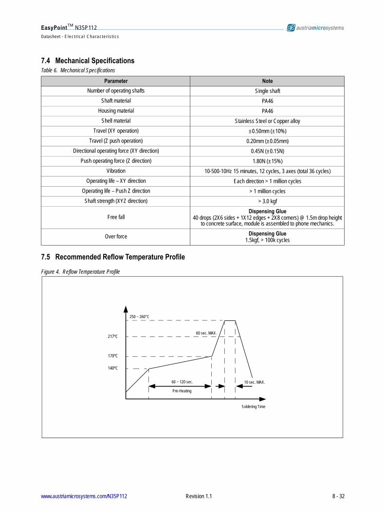
7.5 Recommended Reflow Temperature Profile
Figure 4. Reflow Temperature Profile
Table 6. Mechanical Specifications
Parameter NoteNumber of operating shafts Single shaft
Shaft material PA46Housing material PA46
Shell material Stainless Steel or Copper alloyTravel (XY operation) ±0.50mm (±10%)
Travel (Z push operation) 0.20mm (±0.05mm)Directional operating force (XY direction) 0.45N (±0.15N)
Push operating force (Z direction) 1.80N (±15%)Vibration 10-500-10Hz 15 minutes, 12 cycles, 3 axes (total 36 cycles)
Operating life – XY direction Each direction > 1 million cyclesOperating life – Push Z direction > 1 million cyclesShaft strength (XYZ direction) > 3.0 kgf
Free fallDispensing Glue
40 drops (2X6 sides + 1X12 edges + 2X8 corners) @ 1.5m drop height to concrete surface, module is assembled to phone mechanics.
Over force Dispensing Glue1.5kgf, > 100k cycles
217ºC
170ºC
140ºC
250 ~ 260°C
60 sec. MAX.
60 ~ 120 sec.
Pre-Heating
10 sec. MAX.
Soldering Time
www.austriamicrosystems.com/N35P112 Revision 1.1 8 - 32

EasyPointTM N35P112Datasheet - U s i n g t h e N 3 5 P 11 2 M o d u l e
8 Using the N35P112 Module8.1 Powering up the ModuleThe N35P112 module has a Power ON Reset (POR) cell to monitor the VDD voltage at startup and reset all the internal registers. After the internal reset is completed, the POR cell is disabled in order to save current during normal operation.If VDD drops below 2.7V down to 0.2V, the POR cell will not be enabled back, and the registers will not be correctly reseted or can get random values.
Note: It is highly recommended to control the external RESETn signal by applying a LOW pulse of >100ns once VDD has reached 2.7V and VDDp reached 1.7V.
Figure 5. Power-up Sequence
8.2 Registers InitializationAfter Power Up, the following sequence must be performed:
1. VDD and VDDp Power up, and reached their nominal values (VDD>2.7V, VDDp>1.7V).2. Initialization:
a. RESETn pulse LOW during >100ns, then RESETn HIGH b. Loop check register [0Fh] until the value F0h or F1h is present (reset finished, registers to default values)c. Write value 06h into register [2Dh] → Configure T_ctrl scaling factor for 0.5mm knob displacement
3. Perform an Offset Calibration (X and Y coordinate compensation for zero position)4. Configure the Dead Zone Area for Wake-up function (if needed)5. Configure the wanted Power Mode and INT function into register [0Fh] (Idle mode / Low Power Mode with Timebase configuration, INT
for Wake-up or Coordinates ready)6. X Y coordinates are ready to be read.
External RESETn pin, and without Power on Reset (POR)
0V2.7V
0
VDDp (>1.7V)
VDD
RESETn>100ns >1000us
Inter
nal re
set
comp
leted
Power on Reset (POR) only
0V0.2VVDD
>1000us
Inter
nal re
set
comp
leted
Power up phase
VDD @ t=0 between 0V and 0.2V
2.7V
Power up phase
VDD @ t=0 between 0V and 2.7V
www.austriamicrosystems.com/N35P112 Revision 1.1 9 - 32

EasyPointTM N35P112Datasheet - U s i n g t h e N 3 5 P 11 2 M o d u l e
8.3 C Source Code Example
8.3.1 Initializationvoid EasyPoint_init (void){
unsigned char Reset_status = 0;
RESETn = 0;Delay_ms(1);// RESETn pulse after power upRESETn = 1; Delay_ms(1);
while (Reset_status != 0xF0)// Check the reset has been done{
Reset_status = I2C_Read8(0x40, 0x0F) & 0xFE;}
I2C_Write8(0x40, 0x2d, 0x06); // Scaling factor for N35 (0.5mm knob travel)}
8.3.2 Offset Calibrationvoid Offset_Calibrate (void){
char i;int x_cal=0, y_cal=0;
EA = 0;// Disable the MCU interrupts
I2C_Write8(0x40, 0x0F, 0x00);// Low Power Mode 20ms
Delay_ms(1);
I2C_Read8(0x40, 0x11); // Flush an unused Y_reg to reset the interrupt
for (i=0; i<16; i++)// Read 16 times the coordinates and then average{
while (INTn);// Wait until next interrupt (new coordinates)x_cal += (signed char) I2C_Read8(0x40, 0x10); // Read X positiony_cal += (signed char) I2C_Read8(0x40, 0x11); // Read Y position
}
// offset_X and offset_Y are global variables, used for each coordinate readout in the interrupt routineoffset_X = -(x_cal>>4); // Average X: divide by 16offset_Y = -(y_cal>>4); // Average Y: divide by 16
EA = 1; // Enable the MCU interrupts}
www.austriamicrosystems.com/N35P112 Revision 1.1 10 - 32
EasyPointTM N35P112Datasheet - U s i n g t h e N 3 5 P 11 2 M o d u l e
8.3.3 Dead Zone areaThe dead zone area is set around the zero position of the module. The zero position is known after the offset calibration. The dead zone area is a square with a width of 2*center_threshold, around the calibrated zero position.
void Interrupt_Calibrate (center_threshold) {
EA = 0; // Disable the MCU interruptsI2C_Write8(0x40, 0x12, center_threshold - offset_X ); // Xp registerI2C_Write8(0x40, 0x13, -center_threshold - offset_X); // Xn registerI2C_Write8(0x40, 0x14, center_threshold - offset_Y); // Yp registerI2C_Write8(0x40, 0x15, -center_threshold - offset_Y); // Yn registerEA = 1; // Enable the MCU interrupts
}
8.3.4 Interrupt Routinevoid EasyPoint_interrupt (void) interrupt 0{
int X_temp, Y_temp;
EA=0;// Disable MCU interrupts
/* OPTIONAL: If the module is in a slow power mode (e.g. Wakeup mode INT_function=1 with 320ms rate), configure to a higher rate with INTn for new coordinates ready (e.g. INT_function = 0 with 20ms rate) */
x_reg = I2C_Read8(0x40, 0x10); // Read X positiony_reg = I2C_Read8(0x40, 0x11); // Read Y position with interrupt reset
// Add the X and Y offset for correct recenteringX_temp = x_reg + offset_X; Y_temp = y_reg + offset_Y;
/* OPTIONAL: If X_temp and Y_temp are near the center since a few interrupts, meaning the knob has been released, the module can be put back in a slow power mode (e.g. Wakeup mode INT_function=1 with 320ms rate) */
EA = 1; // Enable the MCU interrupts}
www.austriamicrosystems.com/N35P112 Revision 1.1 11 - 32
EasyPointTM N35P112Datasheet - X Y C o o r d i n a t e s I n t e r p r e t a t i o n
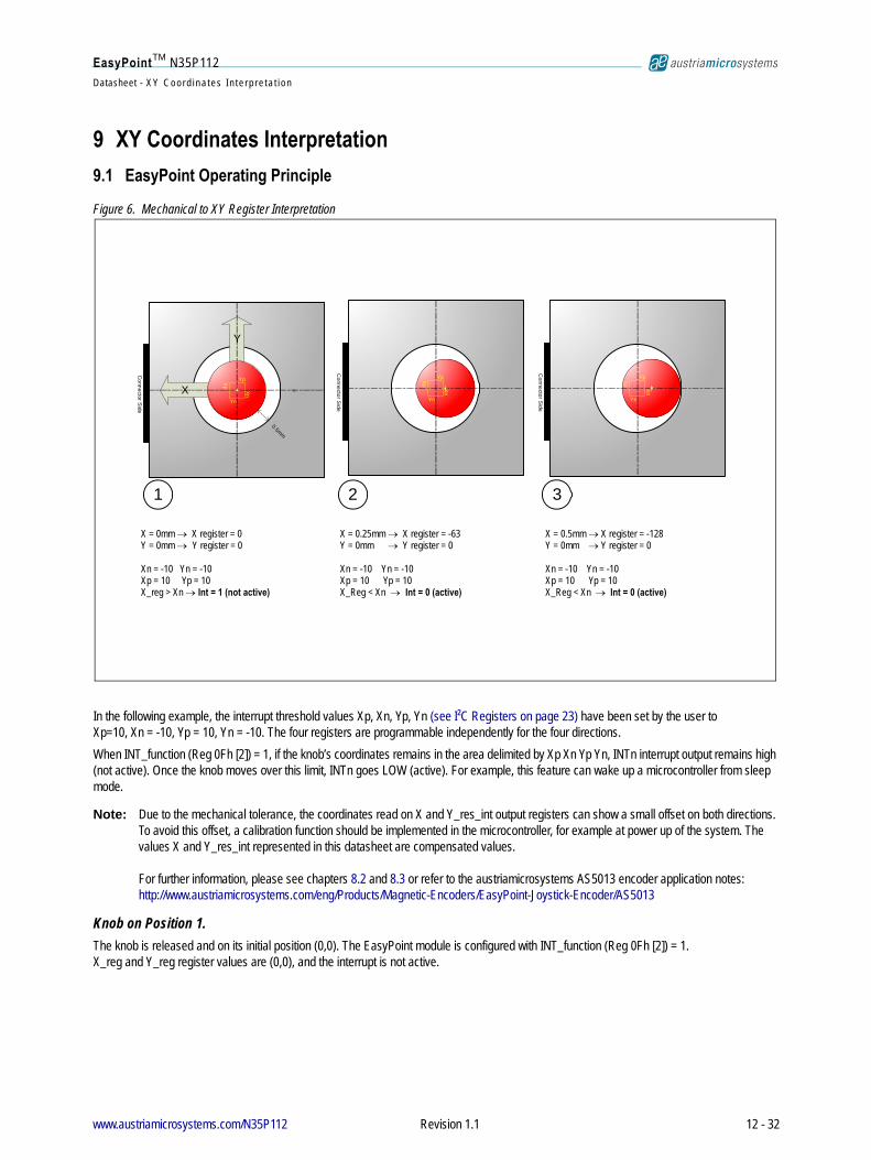
9 XY Coordinates Interpretation9.1 EasyPoint Operating Principle
Figure 6. Mechanical to XY Register Interpretation
In the following example, the interrupt threshold values Xp, Xn, Yp, Yn (see I²C Registers on page 23) have been set by the user to Xp=10, Xn = -10, Yp = 10, Yn = -10. The four registers are programmable independently for the four directions.When INT_function (Reg 0Fh [2]) = 1, if the knob’s coordinates remains in the area delimited by Xp Xn Yp Yn, INTn interrupt output remains high (not active). Once the knob moves over this limit, INTn goes LOW (active). For example, this feature can wake up a microcontroller from sleep mode.
Note: Due to the mechanical tolerance, the coordinates read on X and Y_res_int output registers can show a small offset on both directions. To avoid this offset, a calibration function should be implemented in the microcontroller, for example at power up of the system. The values X and Y_res_int represented in this datasheet are compensated values. For further information, please see chapters 8.2 and 8.3 or refer to the austriamicrosystems AS5013 encoder application notes: http://www.austriamicrosystems.com/eng/Products/Magnetic-Encoders/EasyPoint-Joystick-Encoder/AS5013
Knob on Position 1. The knob is released and on its initial position (0,0). The EasyPoint module is configured with INT_function (Reg 0Fh [2]) = 1. X_reg and Y_reg register values are (0,0), and the interrupt is not active.
X = 0mm → X register = 0Y = 0mm → Y register = 0
Xn = -10 Yn = -10Xp = 10 Yp = 10X_reg > Xn → Int = 1 (not active)
X = 0.25mm → X register = -63Y = 0mm → Y register = 0
Xn = -10 Yn = -10Xp = 10 Yp = 10X_Reg < Xn → Int = 0 (active)
X = 0.5mm → X register = -128Y = 0mm → Y register = 0
Xn = -10 Yn = -10Xp = 10 Yp = 10X_Reg < Xn → Int = 0 (active)
11X
Y
Xn
Xp
Yp
Yn
0.5mm
Connector S
ide
Connector S
ide
Connector S
ide
1 2 3
Xn
Xp
Yp
Yn
Xn
Xp
Yp
Yn
www.austriamicrosystems.com/N35P112 Revision 1.1 12 - 32
EasyPointTM N35P112Datasheet - X Y C o o r d i n a t e s I n t e r p r e t a t i o n
Knob on Position 2. The center of the magnet has been moved upon the horizontal wakeup threshold Xp. The EasyPoint module sets INTn LOW (active). At this point, the microcontroller can configure the module with INT_function (Reg 0Fh [2]) = 0 and change the Low Power timebase Reg 0Fh [6:4] for a faster reaction time. In this interrupt mode, the interrupt output goes LOW (active) each time a new X and Y value is ready to be read by the microcontroller. The interrupt is reseted HIGH (not active) once the register Y_res_int has been read (see I²C Registers on page 23).
Knob on Position 3. The magnet has been moved to the maximum distance from the center (+0.5mm). The maximum X value is -128 decimal.
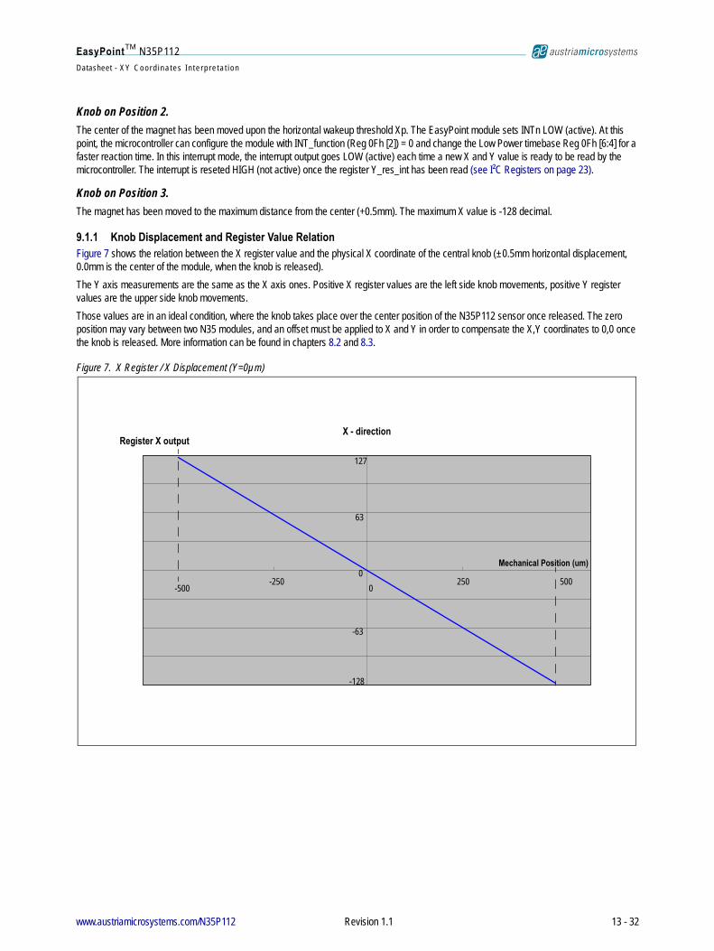
9.1.1 Knob Displacement and Register Value RelationFigure 7 shows the relation between the X register value and the physical X coordinate of the central knob (±0.5mm horizontal displacement, 0.0mm is the center of the module, when the knob is released).The Y axis measurements are the same as the X axis ones. Positive X register values are the left side knob movements, positive Y register values are the upper side knob movements.Those values are in an ideal condition, where the knob takes place over the center position of the N35P112 sensor once released. The zero position may vary between two N35 modules, and an offset must be applied to X and Y in order to compensate the X,Y coordinates to 0,0 once the knob is released. More information can be found in chapters 8.2 and 8.3.
Figure 7. X Register / X Displacement (Y=0µm)
X - direction
-128
-63
0
63
127
-500-250
0250 500
Mechanical Position (um)
Register X output
www.austriamicrosystems.com/N35P112 Revision 1.1 13 - 32
EasyPointTM N35P112Datasheet - X Y C o o r d i n a t e s I n t e r p r e t a t i o n
9.2 Operation Principle
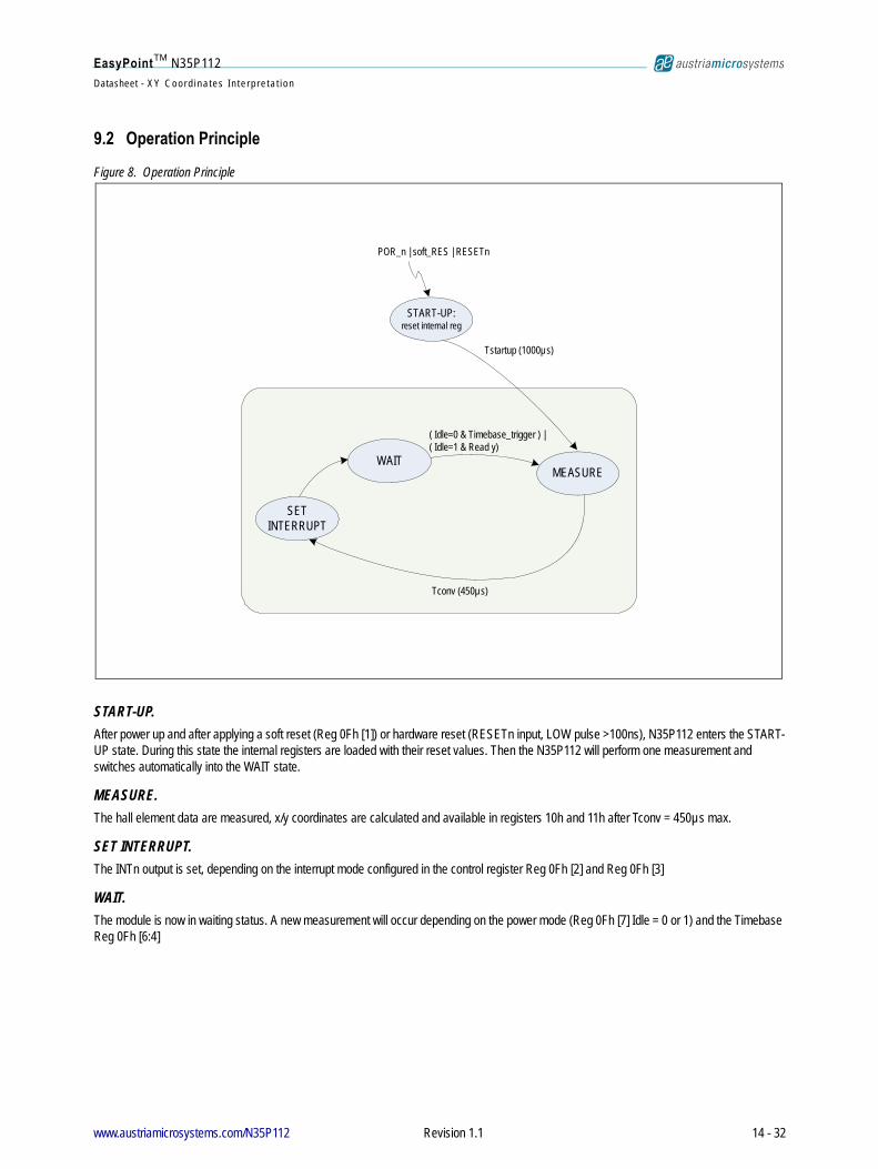
Figure 8. Operation Principle
START-UP. After power up and after applying a soft reset (Reg 0Fh [1]) or hardware reset (RESETn input, LOW pulse >100ns), N35P112 enters the START-UP state. During this state the internal registers are loaded with their reset values. Then the N35P112 will perform one measurement and switches automatically into the WAIT state.
MEASURE. The hall element data are measured, x/y coordinates are calculated and available in registers 10h and 11h after Tconv = 450µs max.
SET INTERRUPT. The INTn output is set, depending on the interrupt mode configured in the control register Reg 0Fh [2] and Reg 0Fh [3]
WAIT. The module is now in waiting status. A new measurement will occur depending on the power mode (Reg 0Fh [7] Idle = 0 or 1) and the Timebase Reg 0Fh [6:4]
POR_n | soft_RES | RESETn
Tstartup (1000µs)
MEASURE
START-UP:reset internal reg
SET INTERRUPT
WAIT
( Idle=0 & Timebase_trigger ) |( Idle=1 & Read y)
Tconv (450µs)
www.austriamicrosystems.com/N35P112 Revision 1.1 14 - 32

EasyPointTM N35P112Datasheet - I ² C i n t e r f a c e
10 I²C interfaceThe N35P112 supports the 2-wire high-speed I²C protocol in device mode, according to the NXP specification UM10204.The host MCU (master) has to initiate the data transfers. The 7-bit device address of the N35P112 depends on the state at the pin ADDR.ADDR = 0 → Slave address =‘1000 000’ (40h)ADDR = 1 → Slave address =‘1000 001’ (41h)For other I²C addresses, please contact austriamicrosystems.Supported modes (slave mode): Random/Sequential Read Byte/Page Write Standard mode : 0 to 100 kHz clock frequency
Fast Mode : 0 to 400 kHz clock frequency High Speed : 0 to 3.4 MHz clock frequency
The SDA signal is bidirectional and is used to read and write the serial data. The SCL signal is the clock generated by the host MCU, to synchronize the SDA data in read and write mode. The maximum I²C clock frequency is 3.4MHz, data are triggered on the rising edge of SCL.
10.1 Interface Operation
Figure 9. I²C Timing Diagram for FS-mode
Figure 10. Timing Diagram for HS-mode
SDA
SCL
StartStop
tBUF
tLOW tR
tHD.STA
tHIGH
tF
tSU.DAT tSU.STA
tHD.STA
tSU.STO
RepeatedStart
tHD.DAT
www.austriamicrosystems.com/N35P112 Revision 1.1 15 - 32

EasyPointTM N35P112Datasheet - I ² C i n t e r f a c e
10.2 I²C Electrical SpecificationStandard-mode, Fast-mode, High Speed-mode
Symbol Parameter Condition Min Max Unit
VIL LOW-Level Input Voltage -0.5 0.3VDDp V
VIH HIGH-Level Input Voltage 0.7VDDp VDDp + 0.51
1. Maximum VIH = VDDpmax +0.5V or 5.5V, which ever is lower.
V
Vhys Hysteresis of Schmitt Trigger Inputs VDDp < 2V 0.1VDDp - V
VOLLOW-Level Output Voltage (open-drain or open-collector) at 3mA Sink Current VDDp < 2V - 0.2VDDp V
ICS Pull-up current of SCLH current source SCLH output levels between0.3VDDp and 0.7VDDp 3 12 mA
tSPPulse Width of Spikes that must be suppressed by the Input Filter - 10 ns
Ii Input Current at each I/O Pin Input Voltage between0.1VDDp and 0.9VDDp - 10 µA
CB Total Capacitive Load for each Bus Line - 400 pF
CI/O I/O Capacitance (SDA, SCL)2
2. For capacitive bus loads between 100pF and 400pF, the timing parameters must be linearly interpolated.
- 10 pF
www.austriamicrosystems.com/N35P112 Revision 1.1 16 - 32

EasyPointTM N35P112Datasheet - I ² C i n t e r f a c e
10.3 I²C Timing
Symbol Parameter ConditionFS-mode HS-mode CB=100pF
HS-mode CB=400pF1
1. For bus line loads Cb between 100 and 400 pF, the timing parameters must be linearly interpolated.
UnitMin Max Min Max Min Max
fSCLK SCL clock Frequency - 400 - 3400 - 1700 kHz
tBUFBus Free Time; time between STOP and START condition
500 - 500 - 500 - ns
tHD;STAHold time; (Repeated) START condition2
2. After this time the first clock is generated.
600 - 160 - 160 - ns
tLOW LOW period of SCL clock 1300 - 160 - 320 - ns
tHIGH HIGH period of SCL clock 600 - 60 - 120 - ns
tSU;STASetup time for a repeated START condition 600 - 160 - 160 - ns
tHD;DAT Data Hold Time3
3. A device must internally provide a minimum hold time (300ns for Fast-mode, 80ns / max 150ns for High-speed mode) for the SDA signal (referred to the VIHmin of the SCL) to bridge the undefined region of the falling edge of SCL.
0 900 0 70 0 150 ns
tSU;DAT Data Setup Time4
4. A fast-mode device can be used in standard-mode system, but the requirement tSU;DAT = 250ns must then be met. This is automatically the case if the device does not stretch the LOW period of the SCL signal. If such a device does stretch the LOW period of the SCL signal, it must output the next data bit to the SDA line tRmax + tSU;DAT = 1000 + 250 = 1250ns before the SCL line is released.
100 - 10 - 10 - ns
trCL Rise time of SCLH signal External pull-up source of 3mA - - 10 40 20 80 ns
trCL1
Rise time of SCLH signal after repeated START condition and after an acknowledge bit
External pull-up source of 3mA - - 10 80 20 160 ns
tRRise time of SDA and SCL signals 20+0.1CB 120 - - - - ns
tFFall time of SDA and SCL signals 20+0.1CB 120 - - - - ns
tSU;STOSetup time for STOP condition 600 - 160 - 160 - ns
VnL Noise margin at LOW level For each connected device (including hysteresis)
0.1VDDp - 0.1VDDp - 0.1VDDp - V
VnHNoise margin at HIGH level 0.2VDDp - 0.2VDDp - 0.2VDDp - V
www.austriamicrosystems.com/N35P112 Revision 1.1 17 - 32

EasyPointTM N35P112Datasheet - I ² C i n t e r f a c e
10.4 I²C ModesThe N35P112 supports the I²C bus protocol. A device that sends data onto the bus is defined as a transmitter and a device receiving data as a receiver. The device that controls the message is called a master. The devices that are controlled by the master are referred to as slaves. A master device that generates the serial clock (SCL), controls the bus access, and generates the START and STOP conditions must control the bus. The N35P112 operates as a slave on the I²C bus. Connections to the bus are made through the open-drain I/O lines SDA and the input SCL. Clock stretching is not included.
10.4.1 Automatic Increment of Address PointerThe N35P112 slave automatically increments the address pointer after each byte transferred. The increase of the address pointer is independent from the address being valid or not.
10.4.2 Invalid AddressesIf the user sets the address pointer to an invalid address, the address byte is not acknowledged. Nevertheless a read or write cycle is possible. The address pointer is increased after each byte.
10.4.3 ReadingWhen reading from a wrong address, the N35P112 slave data returns all zero. The address pointer is increased after each byte. Sequential read over the whole address range is possible including address overflow.
10.4.4 WritingA write to a wrong address is not acknowledged by the N35P112 slave, although the address pointer is increased. When the address pointer points to a valid address again, a successful write accessed is acknowledged. Page write over the whole address range is possible including address overflow.The following bus protocol has been defined: Data transfer may be initiated only when the bus is not busy. During data transfer, the data line must remain stable whenever the clock line is HIGH. Changes in the data line while the clock line is HIGH
are interpreted as start or stop signals.
Accordingly, the following bus conditions have been defined:
Bus Not Busy. Both data and clock lines remain HIGH.
Start Data Transfer. A change in the state of the data line, from HIGH to LOW, while the clock is HIGH, defines a START condition.
Stop Data Transfer. A change in the state of the data line, from LOW to HIGH, while the clock line is HIGH, defines the STOP condition.
Data Valid. The state of the data line represents valid data when, after a START condition, the data line is stable for the duration of the HIGH period of the clock signal. The data on the line must be changed during the LOW period of the clock signal. There is one clock pulse per bit of data. Each data transfer is initiated with a START condition and terminated with a STOP condition. The number of data bytes transferred between START and STOP conditions are not limited, and are determined by the master device. The information is transferred byte-wise and each receiver acknowledges with a ninth bit.
Acknowledge. Each receiving device, when addressed, is obliged to generate an acknowledge after the reception of each byte. The master device must generate an extra clock pulse that is associated with this acknowledge bit. A device that acknowledges must pull down the SDA line during the acknowledge clock pulse in such a way that the SDA line is stable LOW during the HIGH period of the acknowledge-related clock pulse. Of course, setup and hold times must be taken into account. A master must signal an end of READ access to the slave by not generating an acknowledge bit on the last byte that has been clocked out of the slave. In this case, the slave must leave the data line HIGH to enable the master to generate the STOP condition.
www.austriamicrosystems.com/N35P112 Revision 1.1 18 - 32
EasyPointTM N35P112Datasheet - I ² C i n t e r f a c e
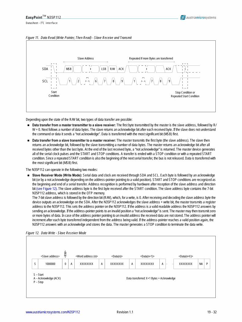
Figure 11. Data Read (Write Pointer, Then Read) - Slave Receive and Transmit
Depending upon the state of the R/W bit, two types of data transfer are possible: Data transfer from a master transmitter to a slave receiver: The first byte transmitted by the master is the slave address, followed by R/
W = 0. Next follows a number of data bytes. The slave returns an acknowledge bit after each received byte. If the slave does not understand the command or data it sends a “not acknowledge”. Data is transferred with the most significant bit (MSB) first.
Data transfer from a slave transmitter to a master receiver: The master transmits the first byte (the slave address). The slave then returns an acknowledge bit, followed by the slave transmitting a number of data bytes. The master returns an acknowledge bit after all received bytes other than the last byte. At the end of the last received byte, a “not acknowledge” is returned. The master device generates all of the serial clock pulses and the START and STOP conditions. A transfer is ended with a STOP condition or with a repeated START condition. Since a repeated START condition is also the beginning of the next serial transfer, the bus is not released. Data is transferred with the most significant bit (MSB) first.
The N35P112 can operate in the following two modes: Slave Receiver Mode (Write Mode): Serial data and clock are received through SDA and SCL. Each byte is followed by an acknowledge
bit (or by a not acknowledge depending on the address-pointer pointing to a valid position). START and STOP conditions are recognized as the beginning and end of a serial transfer. Address recognition is performed by hardware after reception of the slave address and direction bit (see Figure 12). The slave address byte is the first byte received after the START condition. The slave address byte contains the 7-bit N35P112 address, which is stored in the OTP memory. The 7-bit slave address is followed by the direction bit (R/W), which, for a write, is 0. After receiving and decoding the slave address byte the device outputs an acknowledge on the SDA. After the N35P112 acknowledges the slave address + write bit, the master transmits a register address to the N35P112. This sets the address pointer on the N35P112. If the address is a valid readable address the N35P112 answers by sending an acknowledge. If the address-pointer points to an invalid position a “not acknowledge” is sent. The master may then transmit zero or more bytes of data. In case of the address pointer pointing to an invalid address the received data are not stored. The address pointer will increment after each byte transferred independent from the address being valid. If the address-pointer reaches a valid position again, the N35P112 answers with an acknowledge and stores the data. The master generates a STOP condition to terminate the data write.
Figure 12. Data Write - Slave Receiver Mode
1 198762 987
SDA
SCL
StartCondition
Stop Condition or Repeated Start Condition
MSB R/W ACKLSB ACK
Slave Address Repeated if more Bytes are transferred
S 1000000 0 A XXXXXXXX A XXXXXXXX A XXXXXXXX NA
S – StartA – Acknowledge (ACK) Data transferred: X+1 Bytes + AcknowledgeP – Stop
P
<Slave address> <Word address (n)> <Data(n)> <Data(n+X)><RW
>
XXXXXXXX A
<Data(n+1)>
www.austriamicrosystems.com/N35P112 Revision 1.1 19 - 32
EasyPointTM N35P112Datasheet - I ² C i n t e r f a c e
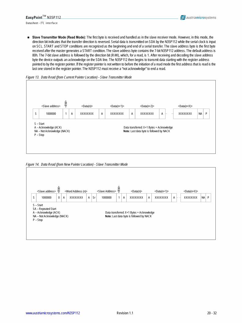
Slave Transmitter Mode (Read Mode): The first byte is received and handled as in the slave receiver mode. However, in this mode, the direction bit indicates that the transfer direction is reversed. Serial data is transmitted on SDA by the N35P112 while the serial clock is input on SCL. START and STOP conditions are recognized as the beginning and end of a serial transfer. The slave address byte is the first byte received after the master generates a START condition. The slave address byte contains the 7-bit N35P112 address. The default address is 80h. The 7-bit slave address is followed by the direction bit (R/W), which, for a read, is 1. After receiving and decoding the slave address byte the device outputs an acknowledge on the SDA line. The N35P112 then begins to transmit data starting with the register address pointed to by the register pointer. If the register pointer is not written to before the initiation of a read mode the first address that is read is the last one stored in the register pointer. The N35P112 must receive a “not acknowledge” to end a read.
Figure 13. Data Read (from Current Pointer Location) - Slave Transmitter Mode
Figure 14. Data Read (from New Pointer Location) - Slave Transmitter Mode
S 1000000 1 A XXXXXXXX A XXXXXXXX A XXXXXXXX NA
S – StartA – Acknowledge (ACK) Data transferred: X+1 Bytes + AcknowledgeNA – Not Acknowledge (NACK) Note: Last data byte is followed by NACKP – Stop
P
<Slave address> <Data(n)> <Data(n+1)> <Data(n+X)><RW
>
XXXXXXXX A
<Data(n+2)>
S 1000000 0 A XXXXXXXX A 1000000 1 XXXXXXXXA
S – StartSA – Repeated StartA – Acknowledge (ACK) Data transferred: X+1 Bytes + AcknowledgeNA – Not Acknowledge (NACK) Note: Last data byte is followed by NACKP – Stop
P
<Slave address> <Word Address (n)> <Slave Address> <Data(n+1)><RW
>
XXXXXXXXA
<Data(n)>
Sr
<RW
>
A XXXXXXXX NA
<Data(n+X)>
www.austriamicrosystems.com/N35P112 Revision 1.1 20 - 32
EasyPointTM N35P112Datasheet - I ² C i n t e r f a c e
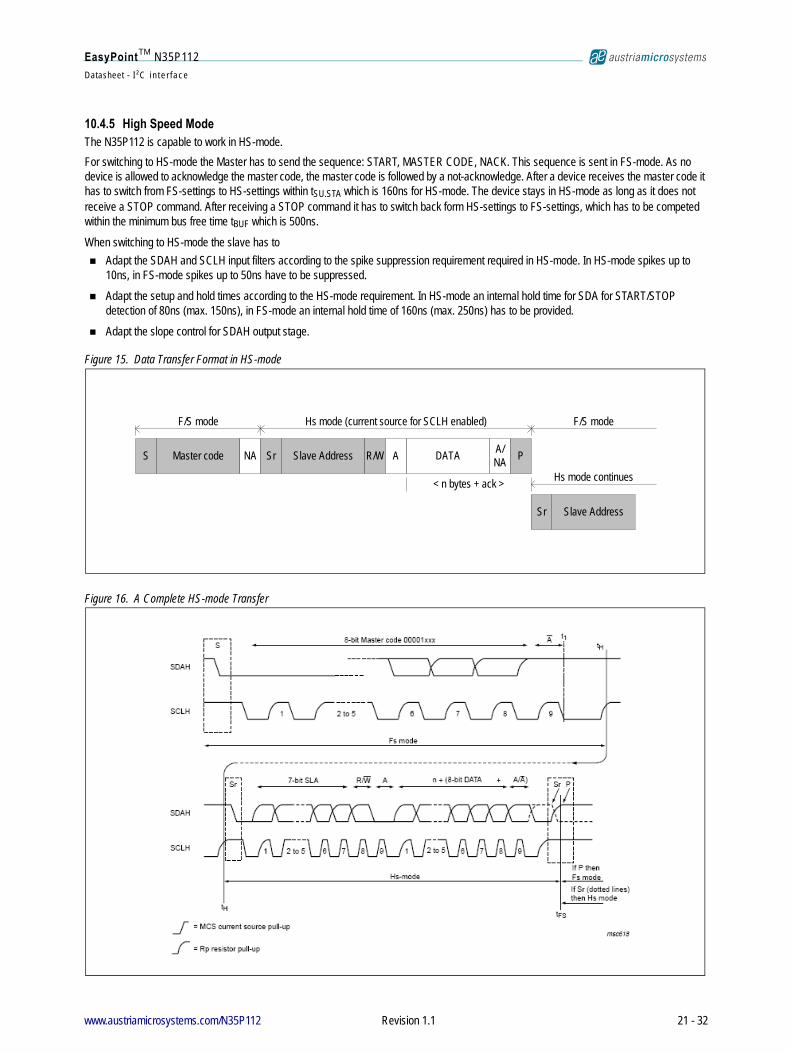
10.4.5 High Speed ModeThe N35P112 is capable to work in HS-mode. For switching to HS-mode the Master has to send the sequence: START, MASTER CODE, NACK. This sequence is sent in FS-mode. As no device is allowed to acknowledge the master code, the master code is followed by a not-acknowledge. After a device receives the master code it has to switch from FS-settings to HS-settings within tSU.STA which is 160ns for HS-mode. The device stays in HS-mode as long as it does not receive a STOP command. After receiving a STOP command it has to switch back form HS-settings to FS-settings, which has to be competed within the minimum bus free time tBUF which is 500ns.
When switching to HS-mode the slave has to Adapt the SDAH and SCLH input filters according to the spike suppression requirement required in HS-mode. In HS-mode spikes up to
10ns, in FS-mode spikes up to 50ns have to be suppressed. Adapt the setup and hold times according to the HS-mode requirement. In HS-mode an internal hold time for SDA for START/STOP
detection of 80ns (max. 150ns), in FS-mode an internal hold time of 160ns (max. 250ns) has to be provided. Adapt the slope control for SDAH output stage.
Figure 15. Data Transfer Format in HS-mode
Figure 16. A Complete HS-mode Transfer
S Master code NA Sr Slave Address R/W DATA A/NA
Slave AddressSr
F/S mode Hs mode (current source for SCLH enabled)
PA
F/S mode
Hs mode continues< n bytes + ack >
www.austriamicrosystems.com/N35P112 Revision 1.1 21 - 32
EasyPointTM N35P112Datasheet - I ² C i n t e r f a c e
10.4.6 Automatic Increment of Address PointerThe N35P112 slave automatically increments the address pointer after each byte transferred. The increase of the address pointer is independent from the address being valid or not.
10.4.7 Invalid AddressesIf the user sets the address pointer to an invalid address, the address byte is not acknowledged. Nevertheless a read or write cycle is possible. The address pointer is increased after each byte.
Reading: When reading from a wrong address, the N35P112 slave returns all zero. The address pointer is increased after each byte. Sequential read over the whole address range is possible including address overflow.
Writing: A write to a wrong address is not acknowledged by the N35P112 slave, although the address pointer is increased. When the address pointer points to a valid address again, a successful write accessed is acknowledged. Page write over the whole address range is possible including address overflow.
10.5 SDA, SCL Input FiltersInput filters for SDA and SCL inputs are included to suppress noise spikes of less than 50ns. Furthermore, the SDA line is delayed by 120ns to provide an internal hold time for Start/Stop detection to bridge the undefined region of the falling edge of SCL. The delay needs to be smaller than tHD.STA 260ns.
For Standard-mode and Fast-mode an internal hold time of 300ns is required, which is not covered by the N35P112 slave.
www.austriamicrosystems.com/N35P112 Revision 1.1 22 - 32
EasyPointTM N35P112Datasheet - I ² C R e g i s t e r s
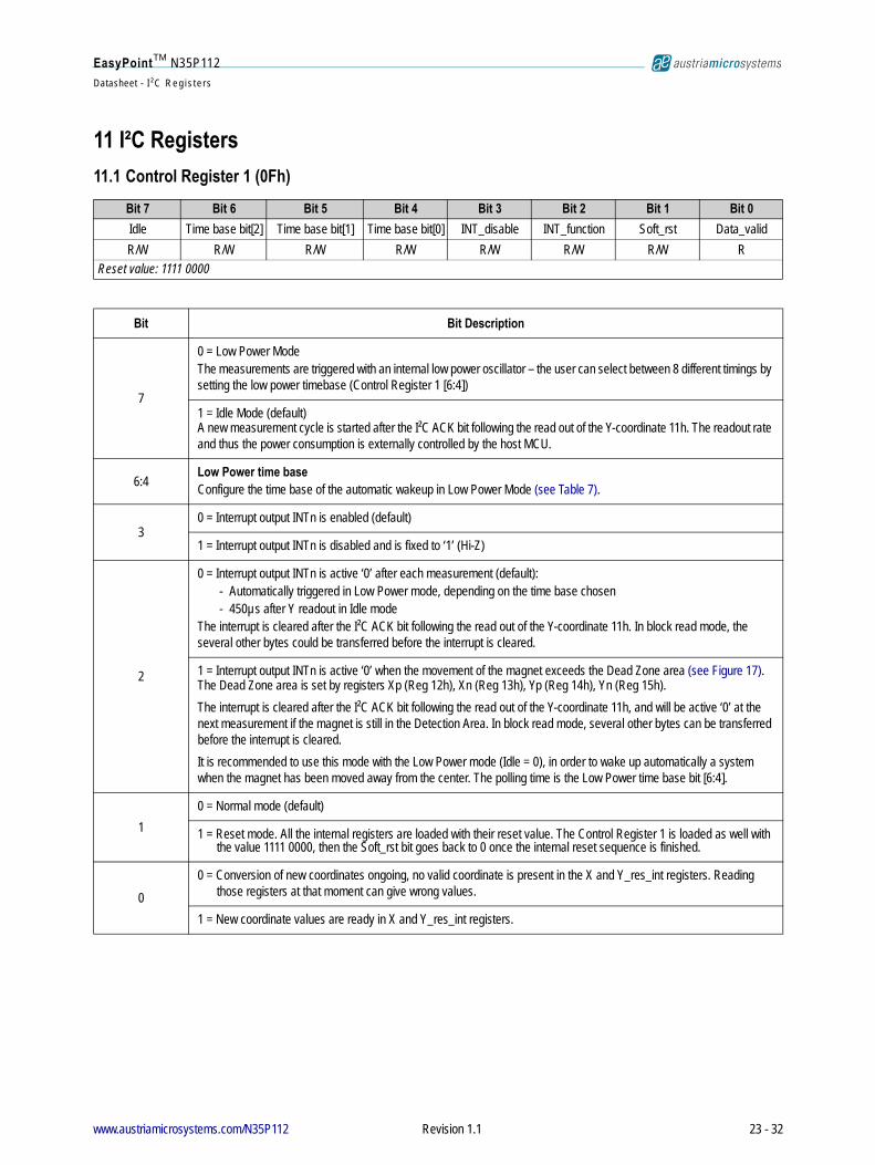
11 I²C Registers11.1 Control Register 1 (0Fh)
Bit 7 Bit 6 Bit 5 Bit 4 Bit 3 Bit 2 Bit 1 Bit 0Idle Time base bit[2] Time base bit[1] Time base bit[0] INT_disable INT_function Soft_rst Data_validR/W R/W R/W R/W R/W R/W R/W R
Reset value: 1111 0000
Bit Bit Description
7
0 = Low Power ModeThe measurements are triggered with an internal low power oscillator – the user can select between 8 different timings by setting the low power timebase (Control Register 1 [6:4])
1 = Idle Mode (default)A new measurement cycle is started after the I²C ACK bit following the read out of the Y-coordinate 11h. The readout rate and thus the power consumption is externally controlled by the host MCU.
6:4Low Power time baseConfigure the time base of the automatic wakeup in Low Power Mode (see Table 7).
30 = Interrupt output INTn is enabled (default)
1 = Interrupt output INTn is disabled and is fixed to ‘1’ (Hi-Z)
2
0 = Interrupt output INTn is active ‘0’ after each measurement (default):- Automatically triggered in Low Power mode, depending on the time base chosen- 450µs after Y readout in Idle mode
The interrupt is cleared after the I²C ACK bit following the read out of the Y-coordinate 11h. In block read mode, the several other bytes could be transferred before the interrupt is cleared.
1 = Interrupt output INTn is active ‘0’ when the movement of the magnet exceeds the Dead Zone area (see Figure 17). The Dead Zone area is set by registers Xp (Reg 12h), Xn (Reg 13h), Yp (Reg 14h), Yn (Reg 15h).The interrupt is cleared after the I²C ACK bit following the read out of the Y-coordinate 11h, and will be active ‘0’ at the next measurement if the magnet is still in the Detection Area. In block read mode, several other bytes can be transferred before the interrupt is cleared.It is recommended to use this mode with the Low Power mode (Idle = 0), in order to wake up automatically a system when the magnet has been moved away from the center. The polling time is the Low Power time base bit [6:4].
10 = Normal mode (default)
1 = Reset mode. All the internal registers are loaded with their reset value. The Control Register 1 is loaded as well with the value 1111 0000, then the Soft_rst bit goes back to 0 once the internal reset sequence is finished.
00 = Conversion of new coordinates ongoing, no valid coordinate is present in the X and Y_res_int registers. Reading
those registers at that moment can give wrong values.
1 = New coordinate values are ready in X and Y_res_int registers.
www.austriamicrosystems.com/N35P112 Revision 1.1 23 - 32

EasyPointTM N35P112Datasheet - I ² C R e g i s t e r s
Figure 17. Dead Zone Representation with INT_function=1
Note: The values in Control Register 1, X_register and Y_res_int register are frozen when the I²C address pointer is set to 0Fh, 10h or 11h. This ensures that the Data_valid bit, X and Y values are taken at the same time. In order to get updated values from those registers, set the address pointer to any other address.
Table 7. Configuration
Low Power time baseCONFIG_REG1 0Fh [6:4]
∆ttimebase
Value Unit000b 20 ms001b 40 ms010b 80 ms011b 100 ms100b 140 ms101b 200 ms110b 260 ms
111b (default) 320 ms
-128127 326496 0 -96-64-32
-128
32
-32
-64
-96
0
96
64
127
Xn
Xp
Yp
Yn
X_reg
Y_reg
Dead zone area, INTn = 1Dete
ction a
rea,
INTn = 0 (
active
)
www.austriamicrosystems.com/N35P112 Revision 1.1 24 - 32

EasyPointTM N35P112Datasheet - I ² C R e g i s t e r s
11.2 X Register (10h)
11.3 Y_res_int Register (11h)
11.4 Xp Register (12h)
11.5 Xn Register (13h)
Bit 7 Bit 6 Bit 5 Bit 4 Bit 3 Bit 2 Bit 1 Bit 0X[7] X[6] X[5] X[4] X[3] X[2] X[1] X[0]R R R R R R R R
Reset value: 0000 0000
Bit Bit Description
7:0 X coordinate, Two’s complement format (signed -128 ~ +127). Positive X values represent left side knob movements.
Bit 7 Bit 6 Bit 5 Bit 4 Bit 3 Bit 2 Bit 1 Bit 0Y[7] Y[6] Y[5] Y[4] Y[3] Y[2] Y[1] Y[0]R R R R R R R R
Reset value: 0000 0000
Bit Bit Description
7:0Y coordinate, Two’s complement format (signed -128~+127).Reading this register will reset the INTn output to Hi-Z, after the ACK bit of Y_res_int register readback.
Bit 7 Bit 6 Bit 5 Bit 4 Bit 3 Bit 2 Bit 1 Bit 0Xp[7] Xp[6] Xp[5] Xp[4] Xp[3] Xp[2] Xp[1] Xp[0]R/W R/W R/W R/W R/W R/W R/W R/W
Reset value: 0000 0101 (5d)
Bit Bit Description
7:0Xp range value, Two’s complement (signed: -128 ~ +127).Determines the LEFT threshold for the activation of INTn output (if output enabled), when bit INT_function = 1 (see Control Register 1 (0Fh) on page 23).
Bit 7 Bit 6 Bit 5 Bit 4 Bit 3 Bit 2 Bit 1 Bit 0Xn[7] Xn[6] Xn[5] Xn[4] Xn[3] Xn[2] Xn[1] Xn[0]R/W R/W R/W R/W R/W R/W R/W R/W
Reset value: 1111 1011 (-5d)
Bit Bit Description
7:0Xn range value, Two’s complement (signed: -128 ~ +127).Determines the RIGHT threshold for the activation of INTn output (if output enabled), when bit INT_function = 1 (see Control Register 1 (0Fh) on page 23).
www.austriamicrosystems.com/N35P112 Revision 1.1 25 - 32

EasyPointTM N35P112Datasheet - I ² C R e g i s t e r s
11.6 Yp Register (14h)
11.7 Yn Register (15h)
11.8 M_ctrl Register (2Bh)
Bit 7 Bit 6 Bit 5 Bit 4 Bit 3 Bit 2 Bit 1 Bit 0Yp[7] Yp[6] Yp[5] Yp[4] Yp[3] Yp[2] Yp[1] Yp[0]R/W R/W R/W R/W R/W R/W R/W R/W
Reset value: 0000 0101 (5d)
Bit Bit Description
7:0Yp range value, Two’s complement (signed: -128 ~ +127).Determines the TOP threshold for the activation of INTn output (if output enabled), when bit INT_function = 1 (see Control Register 1 (0Fh) on page 23).
Bit 7 Bit 6 Bit 5 Bit 4 Bit 3 Bit 2 Bit 1 Bit 0Yn[7] Yn[6] Yn[5] Yn[4] Yn[3] Yn[2] Yn[1] Yn[0]R/W R/W R/W R/W R/W R/W R/W R/W
Reset value: 1111 1011 (-5d)
Bit Bit Description
7:0Yn range value, Two’s complement (signed: -128 ~ +127).Determines the BOTTOM threshold for the activation of INTn output (if output enabled), when bit INT_function = 1 (see Control Register 1 (0Fh) on page 23).
Bit 7 Bit 6 Bit 5 Bit 4 Bit 3 Bit 2 Bit 1 Bit 0M_ctrl[7] M_ctrl[6] M_ctrl[5] M_ctrl[4] M_ctrl[3] M_ctrl[2] M_ctrl[1] M_ctrl[0]
R/W R/W R/W R/W R/W R/W R/W R/WReset value: 0000 0000 (00h)
Bit Bit Description
7:0Middle hall element control register.The M_ctrl register must be set to 00h (default value) after power up for N35P112 module.
www.austriamicrosystems.com/N35P112 Revision 1.1 26 - 32
EasyPointTM N35P112Datasheet - I ² C R e g i s t e r s
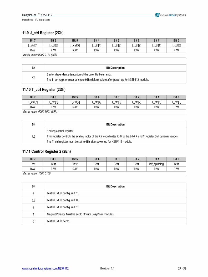
11.9 J_ctrl Register (2Ch)
11.10 T_ctrl Register (2Dh)
11.11 Control Register 2 (2Eh)
Bit 7 Bit 6 Bit 5 Bit 4 Bit 3 Bit 2 Bit 1 Bit 0J_ctrl[7] J_ctrl[6] J_ctrl[5] J_ctrl[4] J_ctrl[3] J_ctrl[2] J_ctrl[1] J_ctrl[0]
R/W R/W R/W R/W R/W R/W R/W R/WReset value: 0000 0110 (06h)
Bit Bit Description
7:0Sector dependent attenuation of the outer Hall elements. The J_ctrl register must be set to 06h (default value) after power up for N35P112 module.
Bit 7 Bit 6 Bit 5 Bit 4 Bit 3 Bit 2 Bit 1 Bit 0T_ctrl[7] T_ctrl[6] T_ctrl[5] T_ctrl[4] T_ctrl[3] T_ctrl[2] T_ctrl[1] T_ctrl[0]
R/W R/W R/W R/W R/W R/W R/W R/WReset value: 0000 1001 (09h)
Bit Bit Description
7:0Scaling control register.This register controls the scaling factor of the XY coordinates to fit to the 8-bit X and Y register (full dynamic range).The T_ctrl register must be set to 06h after power up for N35P112 module.
Bit 7 Bit 6 Bit 5 Bit 4 Bit 3 Bit 2 Bit 1 Bit 0Test Test Test Test Test Test inv_spinning TestR/W R/W R/W R/W R/W R/W R/W R/W
Reset value: 1000 0100
Bit Bit Description
7 Test bit. Must configured ‘1’.
6:3 Test bit. Must configured ‘0’.
2 Test bit. Must configured ‘1’.
1 Magnet Polarity. Must be set to ‘0’ with EasyPoint modules.
0 Test bit. Must be ‘0’.
www.austriamicrosystems.com/N35P112 Revision 1.1 27 - 32
EasyPointTM N35P112Datasheet - I ² C R e g i s t e r s
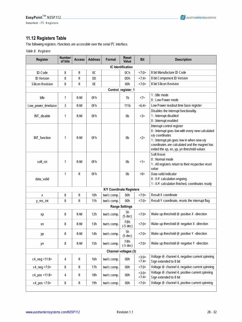
11.12 Registers TableThe following registers / functions are accessible over the serial I²C interface.
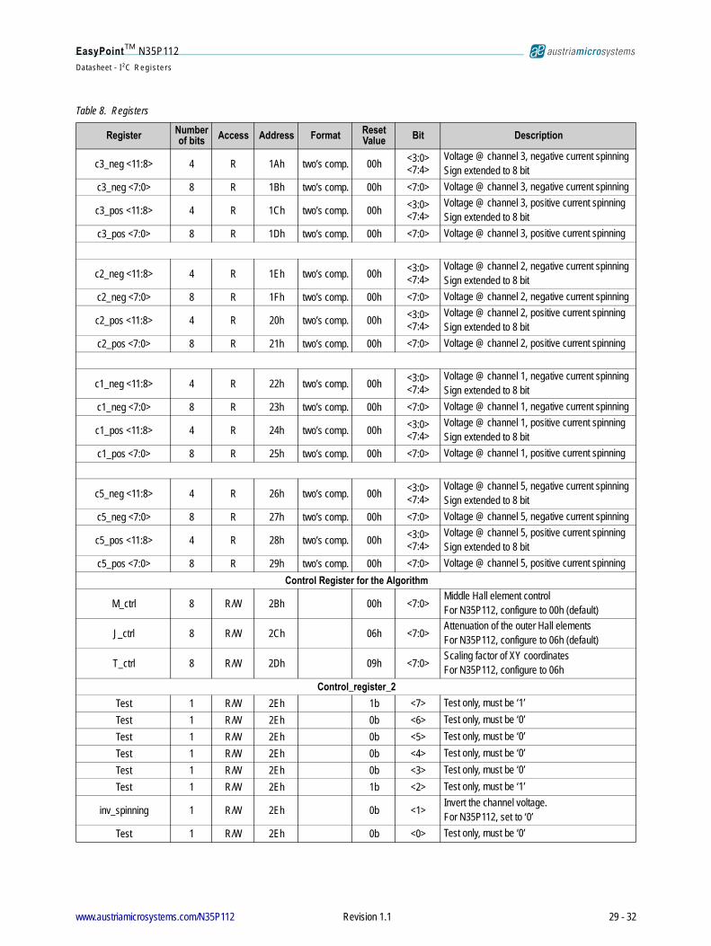
Table 8. Registers
Register Number of bits Access Address Format Reset
Value Bit Description
IC IdentificationID Code 8 R 0C 0Ch <7:0> 8 bit Manufacture ID Code
ID Version 8 R 0D 0Dh <7:4> 8 bit Component ID VersionSilicon Revision 8 R 0E 00h <7:0> 8 bit Silicon Revision
Control_register_1
Idle 1 R/W 0Fh 1b <7>1 : Idle mode 0 : Low Power mode
Low_power_timebase 3 R/W 0Fh 111b <6:4> Low Power readout time base register
INT_disable 1 R/W 0Fh 0b <3>Disables the interrupt functionality. 1 : Interrupt disabled0 : Interrupt enabled
INT_function 1 R/W 0Fh 0b <2>
Interrupt control register 0 : Interrupt goes low with every new calculated x/y coordinates1 : Interrupt pin goes low in when new x/y coordinates are calculated and the magnet has exited the xp, xn, yp, yn threshold values
soft_rst 1 R/W 0Fh 0b <1>
Soft Reset0 : Normal mode 1 : All registers return to their respective reset value
data_valid1 R 0Fh 0b <0> Data valid indicator
0 : X/Y calculation ongoing1 : X/Y calculation finished, coordinates ready
X/Y Coordinate Registersx 8 R 10h two’s comp. 00h <7:0> Result X coordinate
y_res_int 8 R 11h two’s comp. 00h <7:0> Result Y coordinate, resets the interrupt flagRange Settings
xp 8 R/W 12h two’s comp. 5h(5 dec) <7:0> Wake up threshold @ positive X -direction
xn 8 R/W 13h two’s comp. FBh(-5 dec) <7:0> Wake up threshold @ negative X -direction
yp 8 R/W 14h two’s comp. 5h(5 dec) <7:0> Wake up threshold @ positive Y -direction
yn 8 R/W 15h two’s comp. FBh(-5 dec) <7:0> Wake up threshold @ negative Y -direction
Channel voltages (3)
c4_neg <11:8> 4 R 16h two’s comp. 00h <3:0><7:4>
Voltage @ channel 4, negative current spinningSign extended to 8 bit
c4_neg <7:0> 8 R 17h two’s comp. 00h <7:0> Voltage @ channel 4, negative current spinning
c4_pos <11:8> 4 R 18h two’s comp. 00h <3:0><7:4>
Voltage @ channel 4, positive current spinningSign extended to 8 bit
c4_pos <7:0> 8 R 19h two’s comp. 00h <7:0> Voltage @ channel 4, positive current spinning
www.austriamicrosystems.com/N35P112 Revision 1.1 28 - 32
EasyPointTM N35P112Datasheet - I ² C R e g i s t e r s
c3_neg <11:8> 4 R 1Ah two’s comp. 00h <3:0><7:4>
Voltage @ channel 3, negative current spinningSign extended to 8 bit
c3_neg <7:0> 8 R 1Bh two’s comp. 00h <7:0> Voltage @ channel 3, negative current spinning
c3_pos <11:8> 4 R 1Ch two’s comp. 00h <3:0><7:4>
Voltage @ channel 3, positive current spinningSign extended to 8 bit
c3_pos <7:0> 8 R 1Dh two’s comp. 00h <7:0> Voltage @ channel 3, positive current spinning
c2_neg <11:8> 4 R 1Eh two’s comp. 00h <3:0><7:4>
Voltage @ channel 2, negative current spinningSign extended to 8 bit
c2_neg <7:0> 8 R 1Fh two’s comp. 00h <7:0> Voltage @ channel 2, negative current spinning
c2_pos <11:8> 4 R 20h two’s comp. 00h <3:0><7:4>
Voltage @ channel 2, positive current spinningSign extended to 8 bit
c2_pos <7:0> 8 R 21h two’s comp. 00h <7:0> Voltage @ channel 2, positive current spinning
c1_neg <11:8> 4 R 22h two’s comp. 00h <3:0><7:4>
Voltage @ channel 1, negative current spinningSign extended to 8 bit
c1_neg <7:0> 8 R 23h two’s comp. 00h <7:0> Voltage @ channel 1, negative current spinning
c1_pos <11:8> 4 R 24h two’s comp. 00h <3:0><7:4>
Voltage @ channel 1, positive current spinningSign extended to 8 bit
c1_pos <7:0> 8 R 25h two’s comp. 00h <7:0> Voltage @ channel 1, positive current spinning
c5_neg <11:8> 4 R 26h two’s comp. 00h <3:0><7:4>
Voltage @ channel 5, negative current spinningSign extended to 8 bit
c5_neg <7:0> 8 R 27h two’s comp. 00h <7:0> Voltage @ channel 5, negative current spinning
c5_pos <11:8> 4 R 28h two’s comp. 00h <3:0><7:4>
Voltage @ channel 5, positive current spinningSign extended to 8 bit
c5_pos <7:0> 8 R 29h two’s comp. 00h <7:0> Voltage @ channel 5, positive current spinningControl Register for the Algorithm
M_ctrl 8 R/W 2Bh 00h <7:0>Middle Hall element controlFor N35P112, configure to 00h (default)
J_ctrl 8 R/W 2Ch 06h <7:0>Attenuation of the outer Hall elementsFor N35P112, configure to 06h (default)
T_ctrl 8 R/W 2Dh 09h <7:0>Scaling factor of XY coordinatesFor N35P112, configure to 06h
Control_register_2Test 1 R/W 2Eh 1b <7> Test only, must be ‘1’Test 1 R/W 2Eh 0b <6> Test only, must be ‘0’Test 1 R/W 2Eh 0b <5> Test only, must be ‘0’Test 1 R/W 2Eh 0b <4> Test only, must be ‘0’Test 1 R/W 2Eh 0b <3> Test only, must be ‘0’Test 1 R/W 2Eh 1b <2> Test only, must be ‘1’
inv_spinning 1 R/W 2Eh 0b <1>Invert the channel voltage. For N35P112, set to ‘0’
Test 1 R/W 2Eh 0b <0> Test only, must be ‘0’
Table 8. Registers
Register Number of bits Access Address Format Reset
Value Bit Description
www.austriamicrosystems.com/N35P112 Revision 1.1 29 - 32

EasyPointTM N35P112Datasheet - P a c k a g e D r a w i n g s a n d M a r k i n g s
12 Package Drawings and MarkingsFigure 18. N35P112 Dimensions (mm ±0.15)
Figure 19. Recommended PCB Layout (mm ±0.05)
Down
Up
Right
Left (connector side)
www.austriamicrosystems.com/N35P112 Revision 1.1 30 - 32

EasyPointTM N35P112Datasheet - P a c k a g e D r a w i n g s a n d M a r k i n g s
Figure 20. Recommended on Casing Design & Mounting Note
www.austriamicrosystems.com/N35P112 Revision 1.1 31 - 32
EasyPointTM N35P112Datasheet - R e v i s i o n H i s t o r y
Revision History
Note: Typos may not be explicitly mentioned under revision history.
CopyrightsCopyright © 1997-2011, austriamicrosystems AG, Tobelbaderstrasse 30, 8141 Unterpremstaetten, Austria-Europe. Trademarks Registered ®. All rights reserved. The material herein may not be reproduced, adapted, merged, translated, stored, or used without the prior written consent of the copyright owner. All products and companies mentioned are trademarks or registered trademarks of their respective companies.
DisclaimerDevices sold by austriamicrosystems AG are covered by the warranty and patent indemnification provisions appearing in its Term of Sale. austriamicrosystems AG makes no warranty, express, statutory, implied, or by description regarding the information set forth herein or regarding the freedom of the described devices from patent infringement. austriamicrosystems AG reserves the right to change specifications and prices at any time and without notice. Therefore, prior to designing this product into a system, it is necessary to check with austriamicrosystems AG for current information. This product is intended for use in normal commercial applications. Applications requiring extended temperature range, unusual environmental requirements, or high reliability applications, such as military, medical life-support or life-sustaining equipment are specifically not recommended without additional processing by austriamicrosystems AG for each application. For shipments of less than 100 parts the manufacturing flow might show deviations from the standard production flow, such as test flow or test location.The information furnished here by austriamicrosystems AG is believed to be correct and accurate. However, austriamicrosystems AG shall not be liable to recipient or any third party for any damages, including but not limited to personal injury, property damage, loss of profits, loss of use, interruption of business or indirect, special, incidental or consequential damages, of any kind, in connection with or arising out of the furnishing, performance or use of the technical data herein. No obligation or liability to recipient or any third party shall arise or flow out of austriamicrosystems AG rendering of technical or other services.
Contact InformationHeadquartersaustriamicrosystems AG Tobelbaderstrasse 30 A-8141 Unterpremstaetten, AustriaTel: +43 (0) 3136 500 0 Fax: +43 (0) 3136 525 01
For Sales Offices, Distributors and Representatives, please visit: http://www.austriamicrosystems.com/contact
Revision Date Owner Description
0.8 16 Jul, 2010
jlu
Initial release
1.0 01 Dec, 2010 Updated Applications on page 1 and url in the footer
1.1 16 Feb, 2011 Updated sections 8.3.1, 10, 10.2, 10.3, 11.1, 11.3, 11.10, 11.11, 11.12
www.austriamicrosystems.com/N35P112 Revision 1.1 32 - 32