database management systems - degree.pes.edudegree.pes.edu/pdf/2017/bca/digital electronics.pdf ·...
TRANSCRIPT

B.C.A 2017
PES DEGREE COLLEGE BANGALORE SOUTH CAMPUS Affiliated to Bangalore University
DIGITAL ELECTRONICS BCA104T
MODULE SPECIFICATION SHEET
Course Outline
The purpose of the course is to teach principles of digital
electronics. This course covers varieties of topics including
number systems, Boolean algebra, logic families,
combinational and sequential circuits, realisation of Flip
Flops and other related topics. Upon completion, students
should be able to construct, analyze, verify, and
troubleshoot digital circuits using appropriate techniques
and test equipment. Also, this course provides an
introduction of fundamentals of electronics, network
theorems, and AC fundamentals. Within this context it
introduces the Semiconductors and its types,
Semiconductor Diode and types of rectifiers.
Faculty DetailsLAVISHA
Assistant Professor Department of BCA

Page 2 of 11
1. GENERAL INFORMATION
Academic Year : 2017
Semester : I
Title Code Duration
COMPUTER
ARCHITECTURE BCA104T
Lectures 60
Seminars 0
Total: 60
Credits: 02
2. PRE REQUIREMENT STATEMENT
Fundamental knowledge of physics concepts is required.
3. COURSE RELEVANCE
To understand various digital systems and their applications.
To learn about the design principles of different digital electronic circuits.
To study the applications of different digital electronic circuits.
4. LEARNING OUTCOMES
After studying this course, student should be able to:
Analyze different methods used for simplification of Boolean expressions.
Perform decimal, octal, hexadecimal, and binary conversions.
Design and implement Combinational circuits.
Design and implement Sequential circuits.
Use of modern engineering tools, techniques, equipments for designing and testing
Electronics and Communication Engineering systems.
Familiarize with the analysis and design of various electronic circuits along with their
applications in various electronic products.
5. VENUE AND HOURS/WEEK
All lectures will normally be held on VII/VIII Floor.
Lecture Sessions / Week: 05
6. MODULE MAP
Session
#
Modules
(Chapters)
Topic Details Cumulativ
e % of
Portions
Covered
1.
UNIT 1
Chapter 1 –
Fundamentals of
Electronics
Introduction to network theorems and AC fundamentals
2. Ohm’s law: Statement, explanation.
3. Kirchhoff’s law: Statement & explanation of KCL and KVL
4. Mesh/loop analysis (up to 2 loops) and node voltage method,
Numerical problems.

Page 3 of 11
5. Chapter 2 –Network
Theorems
Chapter 3 – AC
Fundamentals
Delta/star and star/Delta transformation: No derivation for
Interco version equations
18%
6.
Introduction of network, port of network (one port network, two
port network), unilateral network, bilateral network, linear
network. Need for application of network theorems.
7.
Superposition theorem: statement, (only with TWO voltage
sources) steps to apply the theorem explanation by considering a
simple resistive network and problems.
8.
Thevenin’s theorem: Statement, (Only with ONE voltage source)
Steps to apply the theorem, explanation by considering a simple
resistive networking and problems.
9.
Norton’s theorem: Statement, (Only with ONE voltage source)
steps to apply the theorem, explanation by considering a simple
resistive network and problems.
10.
Maximum power transfer theorem: Statement, explanation of
theorem by considering a simple resisting network, expression
for maximum power deliver (P L (max) =Vth2/4Rth) (no
derivation) graph of Vs Pl, numerical problems and applications.
11. Reciprocity theorem, Statement, explanation using resistive
network with dc source and numerical problems
12.
AC Fundamentals: Representation of ac sine wave,
instantaneous value, peak value, peak to peak value, average
value, r.m.s value cycle, time period, frequency. (No derivations,
only mention the expressions) Representation of non sinusoidal
waves.
13.
UNIT 2
Chapter 4 -
Semiconductors
Chapter 5 –
Semiconductor Diode
Chapter 6 – Rectifiers
Chapter 7 – Logic
families
Semiconductor Devices: Introduction, atomic structure, energy
level, energy band diagram in solids,
38%
14. classification of conductors, insulators and semiconductors.
Semiconductor, properties, crystal structure of semiconductor,
types – intrinsic and extrinsic semiconductor.
15. Intrinsic semiconductor: Crystal structure (Ge& Si), thermal
generated charges (electron and holes) carriers the effect temp
on their motion.
16. Extrinsic semiconductor: Doping, donor acceptor impurities, c-
type, p-type semiconductor, majority and minority carriers,
their currents, concept of immobile ions.
17. Semiconductor devices : PN junction diode, formation of pn
junction layer, potential barrier, energy level diagram of pn
junction, Biasing of pn junction,
18. behaviour of pn junction under forward and reverse biasing,
break down in pn junction, avalanche and zener break down.
19. Diode characteristics; V-I characteristic, forward and reverse
bias, diode parameters, bulk resistance, knee voltage, static and
dynamic resistance, PIV.
20. Application of diode; As a rectifier, as logic gate, as a switch, etc.

Page 4 of 11
21. Rectifier, types, Half wave Full wave. Half wave rectifier:
Circuit, working, wave forms and expression for ripple factor
and efficiency (no derivation), advantages & disadvantages. 22.
23. Bridge wave rectifier: Circuit, working, wave forms and
expressions for ripple factor and efficiently (no derivation),
advantages & disadvantages.
24. Logic families: Scale of integration, Digital IC’s, classifications,
DTL, TTL, ECL, MOS, CMOS, Mention of features: speed of
operation, power dissipation, propagation delay, fan-in, fan-out.
25.
UNIT 3
Chapter 8 – Number
Systems
Chapter 9 – Binary
Codes
Chapter 10 – Boolean
algebra
Chapter 11 – K Map
Number Systems: Introduction to number systems – positional
and non-positional, Base /Radix. Decimal number system-
Definition, digits, radix/base, Binary number system –Bit Byte,
Conversions: Binary to Decimal and Decimal to Binary.
58%
26. Octal number system- Conversion from Octal to Decimal to
Octal, Octal to Binary and binary to Octal
27. Hexadecimal number system –Conversion : Decimal to Hex, Hex
to decimal, Hex to Binary, Binary to Hex, Octal to Hex, Hex to
Octal
28. Binary, arithmetic –binary addition, subtraction, multiplication
and division (only Integer part).
29. 1’s and 2’s compliment: 2’s complement subtraction.
30.
Binary code: BCD numbers, 8421 code, 2421 code- examples and
applications. Gray code –Conversions-Gray to binary and
Binary to Gray, application of gray code (Mention only). Excess-
3 code – self complimenting property and applications.
31. Definition and nature of ASCII code. Introduction to error
detection and correction code, parity check.
32.
Boolean algebra:-Laws and theorems. AND, OR, NOT Laws,
Commutative law, associative law, distributive law, Duality
theorem. Demorgan’s theorems-Statements, proof using truth
tables;
33. Simplification of Boolean expressions using Boolean laws.
34. Definition of product term, sum term, minterm, maxterm, SOP,
standard POS and Standard POS. Conversion of Boolean
expression to Standard SOP and Standard POS forms.
35. Karnaugh maps-Definition of Karnaugh map, K- map for 2, 3
and 4 variables. Conversion of truth tables into k-map grouping
of cells, redundant groups
36.
Don’t care conditions Karnaugh map technique to solve 3
variable and 4 variable expressions. Simplification of 3 and 4
variable Boolean expression using K-maps (SOP only)
37.
UNIT 4
Logic Gates: AND Gate: Definition, symbol truth table, timing
diagram, Pin diagram of IC 7408.

Page 5 of 11
38.
Chapter 12- Logic
Gates
Chapter 13 –
Combinational Logic
OR Gate: Definition, symbol, truth table, timing diagram of IC
7432.
NOT Gate: Definition symbol, truth table, timing diagram, Pin
diagram of IC 7404.
78%
39. NAND Gate: Definition, symbol, truth table, Pin diagram of IC
7400,
40. NOR Gate: Definition, symbol, truth table, timing diagram, Pin
diagram of IC 7402.
41. Exclusive OR Gate: Definition, symbol, truth table, timing
diagram.
42. Universal gates
43. Combinational logic circuits: Definition, applications.
44. Half Adder and half subtractor: Symbol, Logic circuits using
XOR and basic gates, Truth table,
45. Full Adder and full subtractor: Symbol, Logic circuits using
XOR and basic gates, Truth table,
46. Adder –Subtractor; Logic circuit, Pin diagram IC 7483, IC 7486.
47. Parallel Adder: 4 –bit parallel binary adder BCD adder, IC 7483
NAND –NOR implementation of Adders.
48. UNIT 5
Chapter 14 – Flip
Flops
Chapter 15 - Registers
Sequential Circuits: Importance of clock in digital circuit and
introduction to flip flop. Difference between latch and flip-flop.
100%
49. Qualitative study of level and edge triggering. RS latch
/unlocked, symbol and truth table.
50. RS flip-flop using NAND gate, symbol, truth table and timing
diagram.
51. D flip –flop – Symbol, truth table, Realization of JK flip –flop
using NAND gates, working, and timing diagram.
52. Race around condition, present and clear inputs, pin diagram of
IC 74112.
53. T flip flop-Logic symbol, JK flip flop as a T flip –flop truth table
and timing diagram
54. Master slave flip flop; Logic circuit, truth table and timing
diagram, advantage of M/S flip-flop, pin diagram of IC 7473 IC
7476.
55. Registers: Definition, types of registers-Serial in serial out, serial
in parallel out (Block diagram representation for each), truth
table, timing diagram and speed comparison.
56.
Registers: Definition, types of registers- Parallel in serial out,
Parallel in parallel our shift register (Block diagram
representation for each), truth table, and timing diagram and
speed comparison.

Page 6 of 11
7. RECOMMENDED BOOKS/JOURNALS/WEBSITES
A. Prescribed Textbook:
a. Thomas L.Floyd ,’’Digital Fundamentals”, Peason Education Inc, New Delhi, 2003.
B. Reference Books: a. Morris Mano, “Digital Design”, 5Th Edition, Prentice Hall, 2013.
b. R.P.Jain, “Modern Digital Electronics”, 3rd Edition, Tata Mc Graw Hill, 2003.
c. Bignell and Donovan, “Digital Electronics”, 5th Edition, Thomson Publication, 2007.
.
8. ASSIGNMENTS: A blue book is to be maintained for submitting the assignments.
ASSIGNMENT 1
1. State and explain the Norton's theorem.
2. Derive an expression for resistors in series and parallel.
ASSIGNMENT 2
1. Explain PN junction with neat diagram.
2. Write the difference between intrinsic and extrinsic semiconductors.
ASSIGNMENT 3
1. Compare half wave and full wave rectifiers.
2. What are the characteristics of an IC? And mention the various types of logic
families.
ASSIGNMENT 4
1. State and prove DeMorgan’s theorem.
2. Simplify the following into SOP form using K map and realize using gates.
F (A, B, C, D) = ∑ m (0, 1, 3, 8, 12, 13, 14) + ∑ d (9, 15)
ASSIGNMENT 5
1. What are universal gates? Explain universal property of NAND & NOR gates.
2. Explain full adder and subtractor with neat circuit diagram.
ASSIGNMENT 6
1. Explain the working of JK flip-flop with a neat diagram.
2. Explain different types of shift registers.
9. THEORY ASSESSMENT
A. WRITTEN EXAMINATION
The Theory Examination is for 70 Marks which will be held for duration of 3 Hrs.
The Scheme and Blue Print will be released to the students once the Bangalore
University releases it.

Page 7 of 11
B. CONTINUOUS ASSESSMENT
The Continuous Assessment is conducted as per the following parameters.
Parameter MARKS WEIGHTAGE
%
22 MARKS
Internal Test 50
MARKS
75% 16.5
MARKS
Assignment 10
MARKS
12.5% 2.75
MARKS
Class Test 10
MARKS
12.5% 2.75
MARKS
Total 70
MARKS
100% 22 MARKS
The students are hereby required to note that every internal test weight-age will
calculated for 22 Marks. This includes timely submission of assignments and attending
class tests as conducted.
The Sum of Best Two Performances in Internal Terms will be taken.
Parameter MARKS
Internal Test 01 22
MARKS
Internal Test 02 22
MARKS
Internal Test 03 22
MARKS
Final Internal Marks (Sum of Best Two Marks of the Three
Internal Tests)
44
MARKS
Attendance
>95 %: 06 Marks
90 - 95 %: 05 Marks
85 - 90 %: 04 Marks
80 - 85 %: 03 Marks
75 - 80 %: 02 Marks
06
MARKS
Total 50
MARKS
Page 8 of 11
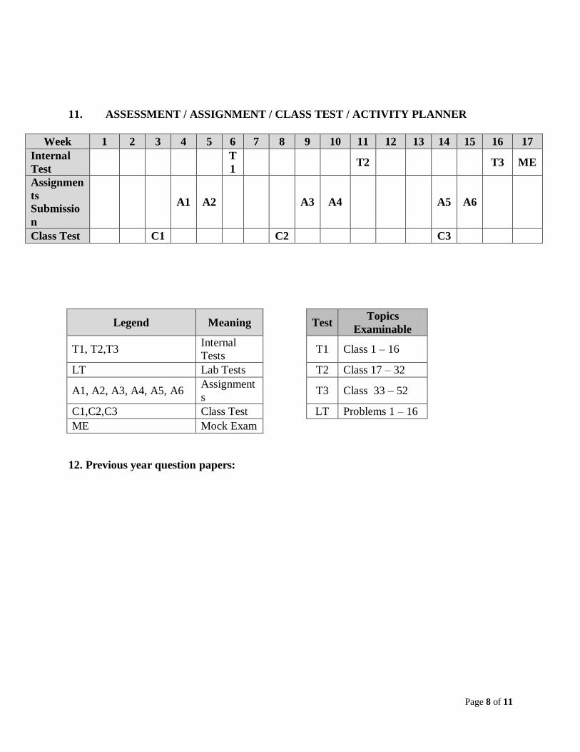
11. ASSESSMENT / ASSIGNMENT / CLASS TEST / ACTIVITY PLANNER
Week 1 2 3 4 5 6 7 8 9 10 11 12 13 14 15 16 17
Internal
Test
T
1 T2 T3 ME
Assignmen
ts
Submissio
n
A1 A2 A3 A4 A5 A6
Class Test C1 C2 C3
Legend Meaning
Test Topics
Examinable
T1, T2,T3 Internal
Tests
T1 Class 1 – 16
LT Lab Tests T2 Class 17 – 32
A1, A2, A3, A4, A5, A6 Assignment
s
T3 Class 33 – 52
C1,C2,C3 Class Test LT Problems 1 – 16
ME Mock Exam
12. Previous year question papers:

Page 9 of 11

Page 10 of 11

Page 11 of 11