data processing and information classification: an in
TRANSCRIPT
Article
Data Processing and Information Classification: anIn-Memory Approach
M. Andrighetti1, G. Turvani1 *, G. Santoro1, M. Vacca1 , A. Marchesin1, F. Ottati1, M. RuoRoch1 ,M. Graziano2 , M. Zamboni1
1 Department of electronics and telecommunication (DET), Politecnico di Torino; Corso Castelfidardo 39,10129 Torino, Italy
2 Department of Applied Science and Technology (DISAT), Politecnico di Torino; Corso Castelfidardo 39,10129 Torino, Italy
* Correspondence: [email protected] (G.T.);
Abstract: To live in the information society means to be surrounded by billions of electronic devicesfull of sensors that constantly acquire data. This enormous amount of data must be processedand classified. A solution commonly adopted is to send these data to server farms to be remotelyelaborated. The drawback is a huge battery drain due to high amount of information that must beexchanged. To compensate this problem data must be processed locally, near the sensor itself. Butthis solution requires huge computational capabilities. While microprocessors, even mobile ones,nowadays have enough computational power, their performance are severely limited by the MemoryWall problem. Memories are too slow, so microprocessors cannot fetch enough data from them,greatly limiting their performance. A solution is the Processing-In-Memory (PIM) approach. Newmemories are designed that are able to elaborate data inside them eliminating the Memory Wallproblem. In this work we present an example of such system, using as a case of study the BitmapIndexing algorithm. Such algorithm is used to classify data coming from many sources in parallel.We propose an hardware accelerator designed around the Processing-In-Memory approach, that iscapable of implementing this algorithm and that can also be reconfigured to do other tasks or to workas standard memory. The architecture has been synthesized using CMOS technology. The results thatwe have obtained highlights that, not only it is possible to process and classify huge amount of datalocally, but also that it is possible to obtain this result with a very low power consumption.
Keywords: Bitmap Indexing, Processing In Memory, Memory wall, Big Data, Internet Of Things
1. Introduction
Nowadays many applications used everyday, defined as data-intensive, require a lot of data toprocess. Examples are the databases manipulation and image processing. This requirement is theeffect of the fast improvement of CMOS technology, that has lead to the creation of very powerful andflexible portable devices. These devices are full of sensors that continuously acquire data. Data can beelaborated remotely by powerful servers, but sending a lot of information through electromagneticwaves requires a huge amount of energy, severely impacting the battery life of mobile devices. Theonly solution is to elaborate data locally, on the mobile device itself.
Thanks to the scaling of transistors size, mobile microprocessors are now theoretically capable ofsuch computation. Unfortunately, memory scaling has been following a different path, resulting still inslow accesses compared to processors computing speed. This discrepancy in performance harms thecomputing abilities of the CPU, since the memory cannot provide data as quickly as required by theCPU. This problem is called Von Neumann bottleneck or Memory Wall. The idea that took form to solve
Preprints (www.preprints.org) | NOT PEER-REVIEWED | Posted: 20 February 2020 doi:10.20944/preprints202002.0294.v1
© 2020 by the author(s). Distributed under a Creative Commons CC BY license.
Peer-reviewed version available at Sensors 2020, 20, 1681; doi:10.3390/s20061681
2 of 13
this problem is to null the distance between processor and memory, removing the cost of data transferand create a unit which is capable of storing information and of performing operation on them. Thisidea takes the name of Processing-in-Memory.
Many in literature have approached the "in-memory" idea. Some narrowing the physical distancebetween memory and computation unit by creating and stacking different layers together. Buteven if the two units are moved very close to each other, they are still distinct components. Othersexploited intrinsic functionality of the memory array or slightly modified peripheral circuitry toperform computation.
Among the many example provided by literature, one of the best fitting representative of the PIMconcept is presented in [1]. In this work the proposed architecture is a memory array in which the cellitself is capable of performing logical operations aimed at solving Convolutional Neural Networks(CNN). In this paper, our main goal is to introduce a proper example of Processing-in-Memory,choosing Bitmap Indexing as an application around which the architecture is shaped. This algorithmhas been chosen because it is used for data classification. This is one of the most important task thatmust be performed by such mobile devices. Being able to classify data allows to understand whichdata must be sent to remote servers and which not, greatly reducing the overall power consumption.The presented architecture is a memory array in which each cell is both capable of storing informationand to perform simple logical operation on them. A characteristic of our architecture is its modularity.The architecture is divided in independent memory banks. A memory bank can work both on itsown or interacting with other banks. Moreover it is possible to build the array with as many banksas needed. This feature lead to great flexibility and high degree of parallelism. The structure waseventually synthesized for analysis purposes, in a 8.5KB square array, using CMOS 45nm and 28nm.The evaluation showed great results, achieving a maximum throughput of 2.45Gop/s and 9.2Gop/srespectively for the two technologies used. This paper is the extended version of the work presentedin the conference Applications in Electronics Pervading Industry, Environment and Society (ApplePie)2019 [2]. In the conference paper the general idea was introduced. Here we greatly expand thearchitecture, moving from the idea to the real implementation.
2. Background
The Processing-in-Memory paradigm was born to solve the Von Neumann bottleneck, which ischaracterized by the gap in performance between memory and processor. Processing-in-Memory thustries to reduce the disparity by merging together storage and processing units. Processing-in-Memory(PIM) can be approached in different ways, depending on the architecture or the technologies to use.A lot of examples can be found in literature, some of them will be depicted in the following, groupedin categories.
2.1. Magnet-based
Magnetic Random Access Memory (MRAM) is a non-volatile memory that uses Magneto-TunnelJunctions as its basic storage element. Thanks to their dual storage-logic properties, MTJs are suitableto implement hybrid logic circuits with CMOS technology suited to implement the PIM principle.In [3] is presented a MTJ-CMOS Full Adder, which compared to a standard only-CMOS solutionshowed better results. In [4] the authors proposed an MTJ-based TCAM, in which the logic part andthe storage element are merged together, and an MTJ-based Non-Volatile FPGA exploiting MTJs andcombinatorial blocks. Both structures resulted in a more compact solution with respect to conventionalones.
In [5] it is proposed a different way to implement Nano Magnetic Logic exploiting the MRAMstructure. Since the basic concept of the NML technology is the transmission of information throughmagnetodynamic interaction between neighbouring magnets, the MRAM structure has been modifiedso that MTJs could interact with each other. Another example is represented by PISOTM [6], an
Preprints (www.preprints.org) | NOT PEER-REVIEWED | Posted: 20 February 2020 doi:10.20944/preprints202002.0294.v1
Peer-reviewed version available at Sensors 2020, 20, 1681; doi:10.3390/s20061681
3 of 13
architecture based on SOT-RAM. It is a reconfigurable architecture in which the main advantage is thatthe storage and logic element result identical and for this reason technology conflict is avoided.
2.2. 3D-Stacking
According to the 3D-Stacking approach multiple layers of DRAM memory are stacked togetherwith a logic layer that can be application-specific ([7],[8]) or general purpose [9]. In [7] the XNOR-POParchitecture was designed to accelerate CNNs for mobile devices. It is composed of Wide-IO2DRAM memory with the logic layer modified according to the XNOR-Net requirements. In [8]it is proposed an architecture for data intensive applications, where a PIM layer made of memoryand application-specific logic is sandwiched between DRAM dies connected together using TSVs. Anexample of general purpose 3D-stacking is 3D-MAPS in [9]. A multi-core structure is used, and everycore is composed of a memory layer and a computing layer.
2.3. ReRAM-based
Resistive RAM is a non-volatile memory that uses a metal-insulator-metal element as storagecomponent. The information is represented by the resistance of the device that can be either high(HRS) or low (LRS). To switch between states the appropriate voltage has to be applied to the cell. Thecommon structure of a ReRAM array is a crossbar, a structure used in matrix-vector multiplication,commonly found in neural networks applications. PRIME [10], an architecture aimed at acceleratingArtificial Neural Networks is an example of this kind of implementations. PRIME is compliant withthe in-memory principle, since the computation is performed directly into the memory array with fewmodifications to the peripheral circuitry. Memory banks are divided intro three sub-arrays each with aspecific role in the architecture. In [11] is proposed a 3D-ReCAM based architecture to accelerate theBLAST algorithm for DNA sequence alignment. The architecture, named RADAR, aims to move theoperations in memory, this way there is no need to transfer the DNA database. In [12] is presented anon-volatile intelligent processor built on a 150 nm CMOS process with HfO RRAM . The structure iscapable of both general computing and the acceleration of neural networks, in fact it is provided witha FCNN Turbo Unit, enhanced with low-power MVM engines to perform FCNN tasks.
Another application that is limited by the Memory Wall problem is Graph Processing. In [13] isproposed a ReRAM-based in-memory architecture as a possible solution. The structure is composedof multiple ReRAM banks, divided into 2 types: graph banks that are used to map the graph andto store its adjacency list and a master bank which stores metadata of the graph banks. This allowsto process the graphs that are stored inside the memory. In [14] is presented PLiM, a programmablesystem composed of a PIM controller and a multi-bank ReRAM which can work both as a standardmemory and as a computational unit, according to the controller signals. PLiM implemented onlyserial operation to keep the controller as simple as possible. In [15] the authors presented ReVAMP, anarchitecture composed of two ReRAM crossbars, supporting parallel computations and VLIW-likeinstructions. To perform logic operations ReVAMP exploits the native properties of ReRAM cells thatimplement a majority voting logic function.
2.4. PIM
In [16] the authors presented TOP-PIM, a system composed of an host processor surrounded byseveral units characterized by 3D-stacked memories with an in-memory processor embedded on thelogic die. In [17] is proposed DIVA, a system in which multiple PIM chips serve as smart-memoryco-processors to a standard microprocessor aimed at improving bandwidth performance fordata intensive applications executing computation directly in memory and enabling a dedicatedcommunication line between the PIM chips. In [18] is presented Terasys, a massively parallel PIMarray. The goal of Terasys was to embed an SIMD PIM array very close to an host processor in orderfor it to be seen both as a processor array and conventional memory. As solution for large-scale graphprocessing performance bottleneck, in [19] the authors proposed Tesseract, a PIM architecture used
Preprints (www.preprints.org) | NOT PEER-REVIEWED | Posted: 20 February 2020 doi:10.20944/preprints202002.0294.v1
Peer-reviewed version available at Sensors 2020, 20, 1681; doi:10.3390/s20061681
4 of 13
as an accelerator for an host processor. Each element of Tesseract has a single-issue in-order core toexecute operations, moreover, the host processor has access to the entire Tesseract’s memory whilsteach core of Tesseract can interact only with its own. Tesseract does not depend on a particular memoryorganization, but it was analyzed exploiting Hybrid Memory Cube (HMC) as baseline. Such a structureproved to perform better than traditional approaches thanks to the fact that Tesseract was able to usemore of the available bandwidth. In [20] is presented Prometheus, a PIM-based framework, whichproposes the approach of distributing data across different vaults in HMC-based systems with thepurpose of reducing energy consumption, improving performance and exploiting the high intra-vaultmemory bandwidth.
In [21] is proposed a solution to accelerate Bulk Bitwise Operations. PINATUBO is an architecturebased on resistive cell memories, such as ReRAMs. The structure is composed of multiple bankswhich are also subdivided into mats. Pinatubo is able to eliminate the movement of data, sincecomputation is performed directly inside memory, executing operations between banks, mats andsubarrays. This way PINATUBO interacts with CPU only for row addresses and control commands.Another example of PIM architecture to accelerate bulk bitwise operations was conceived by theauthors in [22], who presented Ambit, an in-memory accelerator which exploits DRAM technology toachieve total usage of the available bandwidth. The DRAM array is slightly modified to perform AND,OR and NOT operations. Moreover, the CPU can access Ambit directly, this way it is not necessary totransfer data between CPU memory and the accelerator. In [23] is proposed APIM, an ApproximateProcessing-in-Memory architecture which aims to achieve better performance despite a decrease inaccuracy. It is based on emerging non-volatile memories, such as ReRAM and it is composed of across-bar structure grouped in blocks. All the blocks are structurally identical but divided into dataand processing blocks. They are linked together through configurable interconnections. FurthermoreAPIM is able to configure computation precision dynamically, so that it is possible to tune the accuracyruntime.
In [24] is presented ApproxPIM, an HMC-based system in which each vault is independent fromone another and communication with the host processor is based on a parcel transmission protocol.This results in energy and speedup improvements with respect to the used baselines. In [25] theauthors presented MISK, a proposal to reduce the gap between memory and processor. Since datamovement imply a great energy cost, MISK is intended to reduce it by implementing a monolithicstructure, avoiding physical separation between memory and CPU. In fact, MISK is to be integratedinto the cache and it is not conceived to work on its own, but embedded in the CPU. This way it ispossible to achieve great results in terms of energy-per-cycle and execution time. In [26] is introducedGilgamesh, a system based on distributed and shared memory. It is characterized by a multitude ofchips, called MIND chips, which are connected together through a global interconnection network.Each chip is a general purpose unit equipped with multiple DRAM bank and processing logic. In [27]Smart Memory Cube is presented, a PIM processor built near the memory, in particular HMC, whichis connected to an host processor. HMC vault controls are modified to perform atomic operations. ThePIM processor interacts with the host processor so that smaller tasks are executed directly side by sidethe memory.
In [28,29] the authors presented in-memory architectures on which the Advanced EncryptionStandard (AES) algorithm was mapped, showing great result in speed and energy saving comparedto other solutions. In [1] the authors presented an architecture based on the in-memory paradigmaimed at Convolutional Neural Networks (CNN). The structure is a memory array in which each cell isprovided with both storage and computation properties and with the support of an additional weightmemory is designed to support CNN data flow and computation inside the array. This structureshowed great result compared with a conventional CNN accelerator in terms of memory accesses andclock cycles.
Preprints (www.preprints.org) | NOT PEER-REVIEWED | Posted: 20 February 2020 doi:10.20944/preprints202002.0294.v1
Peer-reviewed version available at Sensors 2020, 20, 1681; doi:10.3390/s20061681
5 of 13
C)
B)
NAME
Jane
Harry
Alan
GENDER
F
M
M
STATUS
MARRIED
SINGLE
MARRIED
CAR
SPORT
SPORT
MVP
M
0
1
1
F
1
0
0
MVP
0
0
1
SPORT
1
1
0
BIKE
0
0
0
SPORT
1
1
0
BIKE
0
0
0
M
0
1
1
ANSWER
0
1
0
AND OR =
0
1
0
0
0
1
1
1
0
0
1
0
BIKE
SPORT
M
ANSWER
A)
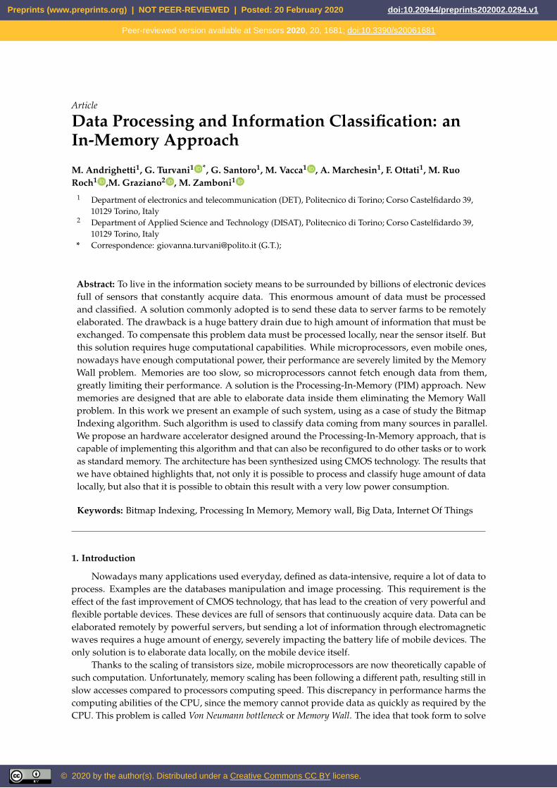
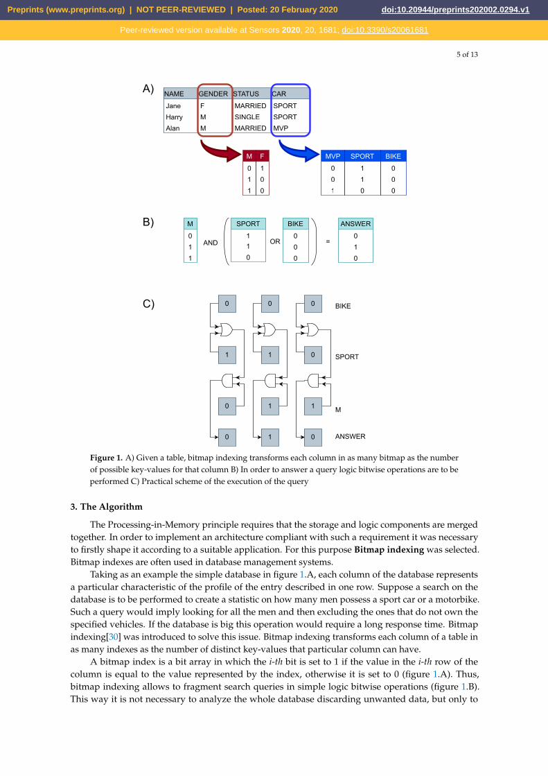
Figure 1. A) Given a table, bitmap indexing transforms each column in as many bitmap as the numberof possible key-values for that column B) In order to answer a query logic bitwise operations are to beperformed C) Practical scheme of the execution of the query
3. The Algorithm
The Processing-in-Memory principle requires that the storage and logic components are mergedtogether. In order to implement an architecture compliant with such a requirement it was necessaryto firstly shape it according to a suitable application. For this purpose Bitmap indexing was selected.Bitmap indexes are often used in database management systems.
Taking as an example the simple database in figure 1.A, each column of the database representsa particular characteristic of the profile of the entry described in one row. Suppose a search on thedatabase is to be performed to create a statistic on how many men possess a sport car or a motorbike.Such a query would imply looking for all the men and then excluding the ones that do not own thespecified vehicles. If the database is big this operation would require a long response time. Bitmapindexing[30] was introduced to solve this issue. Bitmap indexing transforms each column of a table inas many indexes as the number of distinct key-values that particular column can have.
A bitmap index is a bit array in which the i-th bit is set to 1 if the value in the i-th row of thecolumn is equal to the value represented by the index, otherwise it is set to 0 (figure 1.A). Thus,bitmap indexing allows to fragment search queries in simple logic bitwise operations (figure 1.B).This way it is not necessary to analyze the whole database discarding unwanted data, but only to
Preprints (www.preprints.org) | NOT PEER-REVIEWED | Posted: 20 February 2020 doi:10.20944/preprints202002.0294.v1
Peer-reviewed version available at Sensors 2020, 20, 1681; doi:10.3390/s20061681

6 of 13
NAME
GENDER
STATUS
CAR
MARRIED SINGLE MARRIED
Jane Harry Alan
F M M
SPORT SPORT MPV
F
M
1
0
0
1
0
1
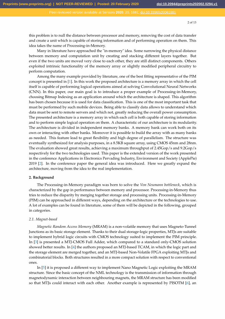
Figure 2. Column-oriented memory organization
operate on selected indexes. Bitmap indexing can provide great results in response time and in storagerequirements since it can be compressed. Bitmap indexing is suited for entries with a number ofpossible values smaller than the depth of the whole table. This technique is most functional for queriesregarding the identification of the position of specific features, for this reason to answer an "how many"query it is necessary to insert a component that counts the hits obtained. Summing up, a query canbe decomposed in simple logic operations which are performed between indexes, processing bitsbelonging to the same position in the array(figure 1.C) .
Clearly, Bitmap indexing results compatible with the Processing-in-Memory paradigm, sinceit is characterized by simple logic bitwise operations and its data format make it easy to embed inmemory. However, bitmap indexing involves operations between columns of a table. If we considermemory organization and imagine to maintain the column-row distribution of the table in memory,this would imply to access multiple rows and then discard all the data that do not belong to the desiredindexes. This approach would be too costly. For this reason for our implementation a column-orientedorganization[31] was preferred, which means that the entire table is stored transposed, so that now,applying bitmap indexing, indexes lie on rows (figure 2).
Thanks to this method, to access an index it is only necessary to access a row and consequentlyoperations between indexes result in operations between memory rows. In this implementation wethus consider the indexes distributed on rows in a memory array. We also take into account two typesof query, simple and composed. A simple query is composed of only one operation (e.g "Who is femaleand married?") whilst a composed one is characterized by intertwined operations (e.g. figure 1.B).Considering the composed query depicted in figure 1.B the operations to perform would be:
1. Access the first operand;2. Access the second operand;3. Execute bitwise operation between the two operands;4. Read result;5. Execute bitwise operation between computed result and third index;6. Count the hits obtained;7. Read final result;
While to answer a simple query only steps 1-4 are needed. The goal is then to implement the justintroduced algorithm directly inside a memory array.
4. The Architecture
The architecture proposed in this paper present a possible solution for the Von Neumannbottleneck implementing a proper in-memory architecture, where logic functions are implementeddirectly inside each memory cell, in contrast with the near-memory approach seen in somestate-of-the-art implementations, where logic operations are performed with logic circuits locatedon the border of the memory array. Moreover, this architecture was intended to overcomethe limits provided by specific technologies by keeping the development of the architecturetechnology-independent, in order to implement a configurable architecture with the highest degree ofparallelism achievable.
A memory array is composed of many storage units, each of which is made of multiple memorycells. Cells are the basic element of the memory itself. Therefore, in order to implement an entirememory array aimed at executing the Bitmap indexing algorithm, firstly it is necessary to define the
Preprints (www.preprints.org) | NOT PEER-REVIEWED | Posted: 20 February 2020 doi:10.20944/preprints202002.0294.v1
Peer-reviewed version available at Sensors 2020, 20, 1681; doi:10.3390/s20061681
7 of 13
DATA...
BANK
BANK
1s COUNTER
ROQ
CONTROL...
BREAKER
LIM ARRAY
AD
DR
. RF
INS
TR
. ME
M.
OP.
DIS
PA
TC
HE
R
0...
0...
QUERIES
DATA_IN
Result of Query
DELAY
A)
OPERATION DECODER
GHOST ROW
LIM ROW
AD
DR
ES
S D
EC
.
LIM CELL
BANK
BREAKER
CELL
MEM CONFIG...
data_in
data_out
from_mem
from_extlogic_result
C)
B)
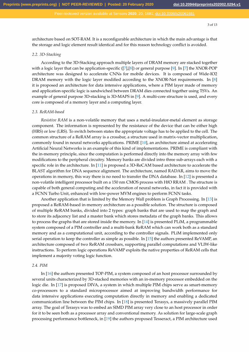
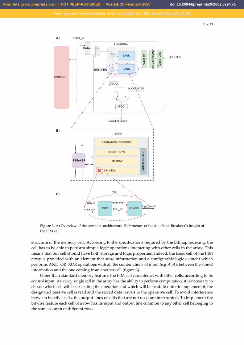
Figure 3. A) Overview of the complete architecture. B) Structure of the duo Bank-Breaker C) Insight ofthe PIM cell
structure of the memory cell. According to the specifications required by the Bitmap indexing, thecell has to be able to perform simple logic operations interacting with other cells in the array. Thismeans that our cell should have both storage and logic properties. Indeed, the basic cell of the PIMarray is provided with an element that store information and a configurable logic element whichperforms AND, OR, XOR operations with all the combinations of input (e.g A, A), between the storedinformation and the one coming from another cell (figure 3).
Other than standard memory features the PIM cell can interact with other cells, according to itscontrol input. As every single cell in the array has the ability to perform computation, it is necessary tochoose which cell will be executing the operation and which will be read. In order to implement it, thedesignated passive cell is read and the stored data travels to the operative cell. To avoid interferencebetween inactive cells, the output lines of cells that are not used are interrupted. To implement thebitwise feature each cell of a row has its input and output line common to any other cell belonging tothe same column of different rows.
Preprints (www.preprints.org) | NOT PEER-REVIEWED | Posted: 20 February 2020 doi:10.20944/preprints202002.0294.v1
Peer-reviewed version available at Sensors 2020, 20, 1681; doi:10.3390/s20061681

8 of 13
In figure 3 the whole structure is depicted. Noticeably, other than the array, the architecture iscomposed of a control unit and some additional components, such as the counter (for counting ones)and register files. Focusing on the array, like any standard memory, it was divided into multiplebanks. Each bank is associated with a breaker that manages data flow from and to the bank. Abank represents the smallest degree of parallelism of the architecture. This means that in a bank itis possible to execute one operation at a time. Thanks to the breakers, each bank is able to workindependently executing operations between its rows or can work with other banks, making interactrows belonging to different banks, while other banks work on different operations in parallel. Asconsequence, supposing each bank in the array works on a different operation by itself, the maximumdegree of parallelism achievable is equal to the number of banks in the array. The Bidirectional Breakeris in charge of managing relations between its bank and the rest of the array. According to the controlinput, the breaker can be passive, i.e. letting data pass through without disturbing its bank so that thebank can work on its own or be silent. The breaker can also be active and diverting data to or from itsbank.
A bank is composed of multiple PIM rows and one Ghost row which is provided only withmemory properties used to store temporary operation results. The Ghost row has the input lineconnected to the logic result output line of the PIM rows, whilst its output line is common with thePIM rows. This way it is possible to read the Ghost row or use its content for further computation.As in standard memories, each row is fragmented in multiple words. This means that operations areactually performed between words belonging to different rows. The result is then temporary saved inthe Ghost word corresponding to the same word address of the word which executed the operation.This was implemented to avoid the need to manage a third address. To handle all the configurationsignals needed to manage the correct execution, two decoders were needed inside each bank. Onethat sets the configuration for the logic operation to execute, sending it to the right row. The secondwas implemented to control addresses, data flow inside the bank and to distinguish between standardmemory mode and PIM operation mode.
In figure 3 it is highlighted that, other than the array, there are some additional components whichare used to guarantee the correct functioning of the entire structure.
The Instruction Memory is used to collect the queries to execute. It consists in a register file, havingas many registers as the number of banks, with an input parallelism equal to the length of a completequery (i.e. two complete addresses and a logic operation configuration string). A composed query istreated as the combination of two distinct queries, which means that a composed query will occupytwo consecutive registers of the Instruction Memory. Clearly, even if the architecture was configuredto exploit its maximum potential by implementing the bitmap indexing algorithm, it can be configuredto perform additional algorithms. For reconfigurability purposes the instruction memory had to beimplemented as wide as possible, but most likely it will not be updated fully each time. In orderto avoid conflicts the Operation Dispatcher is in charge of blocking any old query. Since a query cantake place between any couple of addresses in the array, it is necessary to sent the addresses to theirrespective bank. The Operation Dispatcher thus reorder addresses and sends them to their own bank.After correct reordering, to ensure synchronization the addresses are sampled by the Address RegisterFile which loads the addresses and sends them to the array.
As illustrated previously, results of bitwise logic operations answer to queries in the where clause.To count the number of ones ("1") in the "how many" clause it was inserted a ones counter of logic "1"connected with the output of a delay register. The register was added to ensure timing constraintsgiven by the counter. A simple counter that processes the data input bit-by-bit and increments by onefor each "1" found was too slow. Therefore, a tree-structured counter was implemented. Firstly, thedata array is fragmented into D segments, each of N
D -bits. All segments are then analyzed at the sametime and the ones contained in each segment are counted. Finally, all the factors are added togetherto obtain the final sum. Also, all the adders that form the tree-structure are of the same dimensioncomputed to avoid overflow.
Preprints (www.preprints.org) | NOT PEER-REVIEWED | Posted: 20 February 2020 doi:10.20944/preprints202002.0294.v1
Peer-reviewed version available at Sensors 2020, 20, 1681; doi:10.3390/s20061681

9 of 13
A)
B)
Figure 4. A) Composition of a complete query. B) Preliminary stages of a CLIMA operation
The architecture was conceived to incorporate as many features as possible and at the same timetrying to keep the control circuits as simple as possible. The implemented structure is versatile andcan work in 8 different operation modes, discerned among traditional memory operations and PIMoperations based on the position of the two operands and the desired parallelism: 1) Write; 2) Read; 3)Save result; 4) PIM simple single bank; 5) PIM simple different banks; 6) PIM multiple banks; 7) PIMcomposed; 8) PIM multiple composed. Each operation mode is the starting point of a query, which iscomposed as shown in figure figure 4.A. The FSM chart of all operation modes are reported in figure4.B.
The developed architecture is a modular configurable parallel architecture that implements theconcept of Processing-in-Memory to perform bitwise logic operations directly inside the memory,making it suitable for other applications other than Bitmap indexing, as long as they are based onbitwise.
5. Results and Conclusions
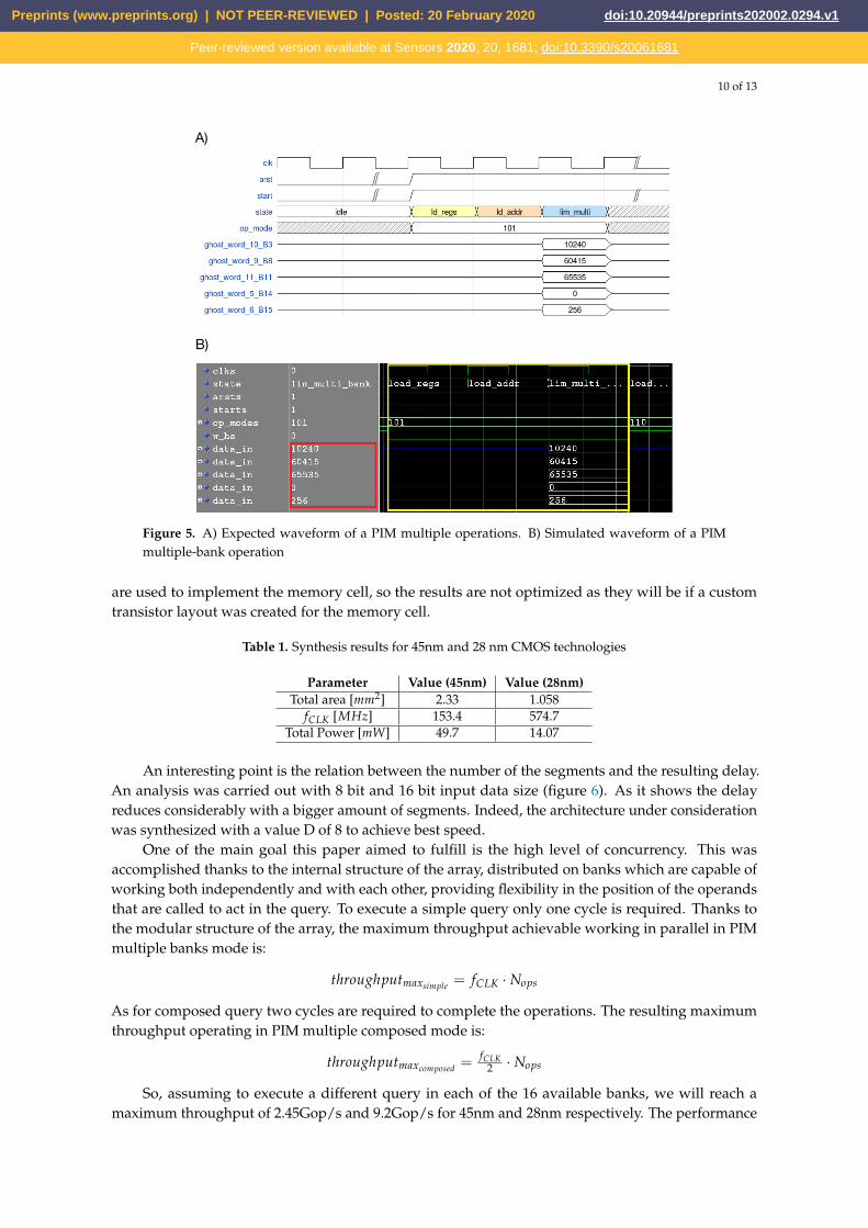
The architecture was fully developed in VHDL (VHSIC Hardware Description Language). Inorder to evaluate its performance a 8.704 KB square memory array was analysed. The array distributionconsisted in 16 banks with 16 bit data size. To ease the simulation process a Matlab program wasdeveloped for the creation of the queries to feed to the PIM architecture. All eight operation modeswere tested with Modelsim to ensure correct functioning. An example of operation mode is reported infigure 5, it shows an example of logic behavior (expcted and simulated) of the proposed architecture.
The architecture was later synthesized with Synopsys Design Compiler using 45nm BULK and28nm FDSOI CMOS technologies (table 1). By using Synopsys Design Compiler latches and logic gates
Preprints (www.preprints.org) | NOT PEER-REVIEWED | Posted: 20 February 2020 doi:10.20944/preprints202002.0294.v1
Peer-reviewed version available at Sensors 2020, 20, 1681; doi:10.3390/s20061681
10 of 13
A)
B)
Figure 5. A) Expected waveform of a PIM multiple operations. B) Simulated waveform of a PIMmultiple-bank operation
are used to implement the memory cell, so the results are not optimized as they will be if a customtransistor layout was created for the memory cell.
Table 1. Synthesis results for 45nm and 28 nm CMOS technologies
Parameter Value (45nm) Value (28nm)Total area [mm2] 2.33 1.058
fCLK [MHz] 153.4 574.7Total Power [mW] 49.7 14.07
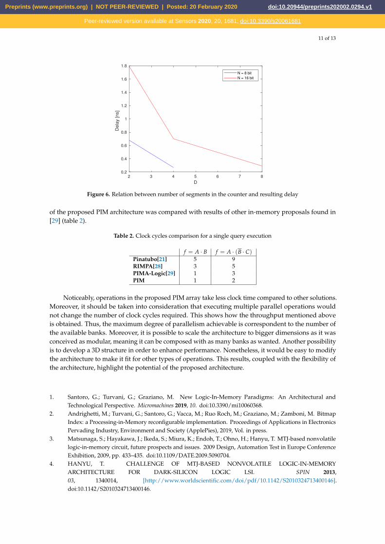
An interesting point is the relation between the number of the segments and the resulting delay.An analysis was carried out with 8 bit and 16 bit input data size (figure 6). As it shows the delayreduces considerably with a bigger amount of segments. Indeed, the architecture under considerationwas synthesized with a value D of 8 to achieve best speed.
One of the main goal this paper aimed to fulfill is the high level of concurrency. This wasaccomplished thanks to the internal structure of the array, distributed on banks which are capable ofworking both independently and with each other, providing flexibility in the position of the operandsthat are called to act in the query. To execute a simple query only one cycle is required. Thanks tothe modular structure of the array, the maximum throughput achievable working in parallel in PIMmultiple banks mode is:
throughputmaxsimple = fCLK · Nops
As for composed query two cycles are required to complete the operations. The resulting maximumthroughput operating in PIM multiple composed mode is:
throughputmaxcomposed = fCLK2 · Nops
So, assuming to execute a different query in each of the 16 available banks, we will reach amaximum throughput of 2.45Gop/s and 9.2Gop/s for 45nm and 28nm respectively. The performance
Preprints (www.preprints.org) | NOT PEER-REVIEWED | Posted: 20 February 2020 doi:10.20944/preprints202002.0294.v1
Peer-reviewed version available at Sensors 2020, 20, 1681; doi:10.3390/s20061681
11 of 13
2 3 4 5 6 7 8
D
0.2
0.4
0.6
0.8
1
1.2
1.4
1.6
1.8
De
lay [
ns]
N = 8 bit
N = 16 bit
Figure 6. Relation between number of segments in the counter and resulting delay
of the proposed PIM architecture was compared with results of other in-memory proposals found in[29] (table 2).
Table 2. Clock cycles comparison for a single query execution
f = A · B f = A · (B · C)Pinatubo[21] 5 9RIMPA[28] 3 5PIMA-Logic[29] 1 3PIM 1 2
Noticeably, operations in the proposed PIM array take less clock time compared to other solutions.Moreover, it should be taken into consideration that executing multiple parallel operations wouldnot change the number of clock cycles required. This shows how the throughput mentioned aboveis obtained. Thus, the maximum degree of parallelism achievable is correspondent to the number ofthe available banks. Moreover, it is possible to scale the architecture to bigger dimensions as it wasconceived as modular, meaning it can be composed with as many banks as wanted. Another possibilityis to develop a 3D structure in order to enhance performance. Nonetheless, it would be easy to modifythe architecture to make it fit for other types of operations. This results, coupled with the flexibility ofthe architecture, highlight the potential of the proposed architecture.
1. Santoro, G.; Turvani, G.; Graziano, M. New Logic-In-Memory Paradigms: An Architectural andTechnological Perspective. Micromachines 2019, 10. doi:10.3390/mi10060368.
2. Andrighetti, M.; Turvani, G.; Santoro, G.; Vacca, M.; Ruo Roch, M.; Graziano, M.; Zamboni, M. BitmapIndex: a Processing-in-Memory reconfigurable implementation. Proceedings of Applications in ElectronicsPervading Industry, Environment and Society (ApplePies), 2019, Vol. in press.
3. Matsunaga, S.; Hayakawa, J.; Ikeda, S.; Miura, K.; Endoh, T.; Ohno, H.; Hanyu, T. MTJ-based nonvolatilelogic-in-memory circuit, future prospects and issues. 2009 Design, Automation Test in Europe ConferenceExhibition, 2009, pp. 433–435. doi:10.1109/DATE.2009.5090704.
4. HANYU, T. CHALLENGE OF MTJ-BASED NONVOLATILE LOGIC-IN-MEMORYARCHITECTURE FOR DARK-SILICON LOGIC LSI. SPIN 2013,03, 1340014, [http://www.worldscientific.com/doi/pdf/10.1142/S2010324713400146].doi:10.1142/S2010324713400146.
Preprints (www.preprints.org) | NOT PEER-REVIEWED | Posted: 20 February 2020 doi:10.20944/preprints202002.0294.v1
Peer-reviewed version available at Sensors 2020, 20, 1681; doi:10.3390/s20061681

12 of 13
5. Turvani, G.; Bollo, M.; Vacca, M.; Cairo, F.; Zamboni, M.; Graziano, M. Design of MRAM-Based MagneticLogic Circuits. IEEE Transactions on Nanotechnology 2017, 16, 851–859. doi:10.1109/TNANO.2016.2641444.
6. Chang, L.; Wang, Z.; Zhang, Y.; Zhao, W. Reconfigurable processing in memory architecture based on spinorbit torque. 2017 IEEE/ACM International Symposium on Nanoscale Architectures (NANOARCH), 2017,pp. 95–96. doi:10.1109/NANOARCH.2017.8053713.
7. Jiang, L.; Kim, M.; Wen, W.; Wang, D. XNOR-POP: A processing-in-memory architecture for binaryConvolutional Neural Networks in Wide-IO2 DRAMs. 2017 IEEE/ACM International Symposium on LowPower Electronics and Design (ISLPED), 2017, pp. 1–6. doi:10.1109/ISLPED.2017.8009163.
8. Zhu, Q.; Akin, B.; Sumbul, H.E.; Sadi, F.; Hoe, J.C.; Pileggi, L.; Franchetti, F. A 3D-stacked logic-in-memoryaccelerator for application-specific data intensive computing. 2013 IEEE International 3D SystemsIntegration Conference (3DIC), 2013, pp. 1–7. doi:10.1109/3DIC.2013.6702348.
9. Kim, D.H.; Athikulwongse, K.; Healy, M.B.; Hossain, M.M.; Jung, M.; Khorosh, I.; Kumar, G.; Lee,Y.J.; Lewis, D.L.; Lin, T.W.; Liu, C.; Panth, S.; Pathak, M.; Ren, M.; Shen, G.; Song, T.; Woo, D.H.;Zhao, X.; Kim, J.; Choi, H.; Loh, G.H.; Lee, H.H.S.; Lim, S.K. Design and Analysis of 3D-MAPS (3DMassively Parallel Processor with Stacked Memory). IEEE Transactions on Computers 2015, 64, 112–125.doi:10.1109/TC.2013.192.
10. Chi, P.; Li, S.; Xu, C.; Zhang, T.; Zhao, J.; Liu, Y.; Wang, Y.; Xie, Y. PRIME: A NovelProcessing-in-Memory Architecture for Neural Network Computation in ReRAM-Based Main Memory.2016 ACM/IEEE 43rd Annual International Symposium on Computer Architecture (ISCA), 2016, pp. 27–39.doi:10.1109/ISCA.2016.13.
11. Huangfu, W.; Li, S.; Hu, X.; Xie, Y. RADAR: A 3D-ReRAM based DNA Alignment AcceleratorArchitecture. 2018 55th ACM/ESDA/IEEE Design Automation Conference (DAC), 2018, pp. 1–6.doi:10.1109/DAC.2018.8465882.
12. Su, F.; Chen, W.H.; Xia, L.; Lo, C.P.; Tang, T.; Wang, Z.; Hsu, K.H.; Cheng, M.; Li, J.Y.; Xie, Y.; Wang, Y.;Chang, M.F.; Yang, H.; Liu, Y. A 462GOPs/J RRAM-based nonvolatile intelligent processor for energyharvesting IoE system featuring nonvolatile logics and processing-in-memory. 2017 Symposium on VLSITechnology, 2017, pp. T260–T261. doi:10.23919/VLSIT.2017.7998149.
13. Han, L.; Shen, Z.; Shao, Z.; Huang, H.H.; Li, T. A novel ReRAM-based processing-in-memory architecturefor graph computing. 2017 IEEE 6th Non-Volatile Memory Systems and Applications Symposium(NVMSA), 2017, pp. 1–6. doi:10.1109/NVMSA.2017.8064464.
14. Gaillardon, P.E.; Amarú, L.; Siemon, A.; Linn, E.; Waser, R.; Chattopadhyay, A.; Micheli, G.D. TheProgrammable Logic-in-Memory (PLiM) computer. 2016 Design, Automation Test in Europe ConferenceExhibition (DATE), 2016, pp. 427–432.
15. Bhattacharjee, D.; Devadoss, R.; Chattopadhyay, A. ReVAMP: ReRAM based VLIW architecture forin-memory computing. Design, Automation Test in Europe Conference Exhibition (DATE), 2017, 2017, pp.782–787. doi:10.23919/DATE.2017.7927095.
16. Zhang, D.; Jayasena, N.; Lyashevsky, A.; Greathouse, J.L.; Xu, L.; Ignatowski, M. TOP-PIM:Throughput-oriented Programmable Processing in Memory. Proceedings of the 23rd InternationalSymposium on High-performance Parallel and Distributed Computing; ACM: New York, NY, USA,2014; HPDC ’14, pp. 85–98. doi:10.1145/2600212.2600213.
17. Draper, J.; Chame, J.; Hall, M.; Steele, C.; Barrett, T.; LaCoss, J.; Granacki, J.; Shin, J.; Chen, C.; Kang, C.W.;Kim, I.; Daglikoca, G. The Architecture of the DIVA Processing-in-memory Chip. Proceedings of the16th International Conference on Supercomputing; ACM: New York, NY, USA, 2002; ICS ’02, pp. 14–25.doi:10.1145/514191.514197.
18. Gokhale, M.; Holmes, B.; Iobst, K. Processing in memory: the Terasys massively parallel PIM array.Computer 1995, 28, 23–31. doi:10.1109/2.375174.
19. Ahn, J.; Hong, S.; Yoo, S.; Mutlu, O.; Choi, K. A scalable processing-in-memory accelerator for parallelgraph processing. 2015 ACM/IEEE 42nd Annual International Symposium on Computer Architecture(ISCA), 2015, pp. 105–117. doi:10.1145/2749469.2750386.
20. Xiao, Y.; Nazarian, S.; Bogdan, P. Prometheus: Processing-in-memory heterogeneous architecture designfrom a multi-layer network theoretic strategy. 2018 Design, Automation Test in Europe ConferenceExhibition (DATE), 2018, pp. 1387–1392. doi:10.23919/DATE.2018.8342229.
Preprints (www.preprints.org) | NOT PEER-REVIEWED | Posted: 20 February 2020 doi:10.20944/preprints202002.0294.v1
Peer-reviewed version available at Sensors 2020, 20, 1681; doi:10.3390/s20061681

13 of 13
21. Li, S.; Xu, C.; Zou, Q.; Zhao, J.; Lu, Y.; Xie, Y. Pinatubo: A processing-in-memory architecture for bulkbitwise operations in emerging non-volatile memories. 2016 53nd ACM/EDAC/IEEE Design AutomationConference (DAC), 2016, pp. 1–6. doi:10.1145/2897937.2898064.
22. Seshadri, V.; Lee, D.; Mullins, T.; Hassan, H.; Boroumand, A.; Kim, J.; Kozuch, M.A.; Mutlu, O.; Gibbons,P.B.; Mowry, T.C. Ambit: In-memory Accelerator for Bulk Bitwise Operations Using Commodity DRAMTechnology. Proceedings of the 50th Annual IEEE/ACM International Symposium on Microarchitecture;ACM: New York, NY, USA, 2017; MICRO-50 ’17, pp. 273–287. doi:10.1145/3123939.3124544.
23. Imani, M.; Gupta, S.; Rosing, T. Ultra-Efficient Processing In-Memory for Data Intensive Applications.Proceedings of the 54th Annual Design Automation Conference 2017; ACM: New York, NY, USA, 2017;DAC ’17, pp. 6:1–6:6. doi:10.1145/3061639.3062337.
24. Tang, Y.; Wang, Y.; Li, H.; Li, X. ApproxPIM: Exploiting realistic 3D-stacked DRAM for energy-efficientprocessing in-memory. 2017 22nd Asia and South Pacific Design Automation Conference (ASP-DAC),2017, pp. 396–401. doi:10.1109/ASPDAC.2017.7858355.
25. Yang, K.; Karam, R.; Bhunia, S. Interleaved logic-in-memory architecture for energy-efficient fine-graineddata processing. 2017 IEEE 60th International Midwest Symposium on Circuits and Systems (MWSCAS),2017, pp. 409–412. doi:10.1109/MWSCAS.2017.8052947.
26. Sterling, T.L.; Zima, H.P. Gilgamesh: A Multithreaded Processor-In-Memory Architecture for PetaflopsComputing. Supercomputing, ACM/IEEE 2002 Conference, 2002, pp. 48–48. doi:10.1109/SC.2002.10061.
27. Azarkhish, E.; Rossi, D.; Loi, I.; Benini, L. Design and Evaluation of a Processing-in-Memory Architecturefor the Smart Memory Cube. Proceedings of the 29th International Conference on Architecture ofComputing Systems – ARCS 2016 - Volume 9637; Springer-Verlag New York, Inc.: New York, NY, USA,2016; pp. 19–31. doi:10.1007/978-3-319-30695-7_2.
28. Angizi, S.; He, Z.; Parveen, F.; Fan, D. RIMPA: A New Reconfigurable Dual-Mode In-Memory ProcessingArchitecture with Spin Hall Effect-Driven Domain Wall Motion Device. 2017 IEEE Computer SocietyAnnual Symposium on VLSI (ISVLSI), 2017, pp. 45–50. doi:10.1109/ISVLSI.2017.18.
29. Angizi, S.; He, Z.; Fan, D. PIMA-Logic: A Novel Processing-in-Memory Architecture for Highly Flexibleand Energy-Efficient Logic Computation. 2018 55th ACM/ESDA/IEEE Design Automation Conference(DAC), 2018, pp. 1–6. doi:10.1109/DAC.2018.8465706.
30. https://docs.oracle.com/cd/A84870_01/doc/server.816/a76994/indexes.htm.31. https://en.wikipedia.org/wiki/Column-oriented_DBMS.
Preprints (www.preprints.org) | NOT PEER-REVIEWED | Posted: 20 February 2020 doi:10.20944/preprints202002.0294.v1
Peer-reviewed version available at Sensors 2020, 20, 1681; doi:10.3390/s20061681