data acquisition and monitoring for sipm based imaging camera
TRANSCRIPT
Data Acquisition and Monitoring for SiPM based Imaging CameraSandeep Kumar Duhana,b,*; S. S. Upadhyaa; K. S. Gothea, S. K. Raoa, B. B. Singha, M. Ranjana, B. K. Nagesha, N. K. Parmara, M. N. Sarafa, B. S. Acharyaa, V. Bhatnagarb
aDepartment of High Energy Physics, Tata Institute of Fundamental Research, Colaba, Mumbai - 400005bDepartment of Physics, Panjab University, Chandigarh - 160014, India
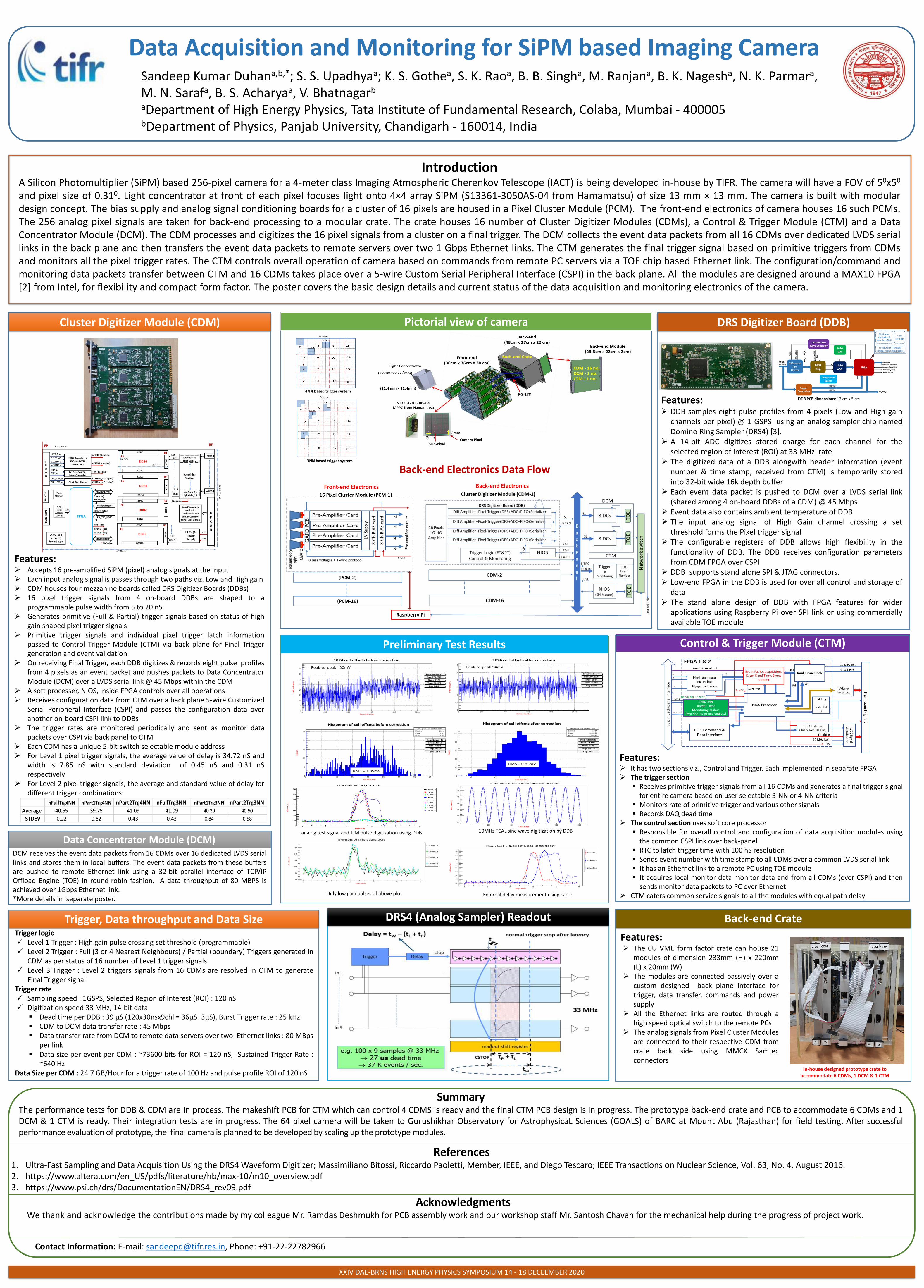
Features: Accepts 16 pre-amplified SiPM (pixel) analog signals at the input Each input analog signal is passes through two paths viz. Low and High gain CDM houses four mezzanine boards called DRS Digitizer Boards (DDBs) 16 pixel trigger signals from 4 on-board DDBs are shaped to a
programmable pulse width from 5 to 20 nS Generates primitive (Full & Partial) trigger signals based on status of high
gain shaped pixel trigger signals Primitive trigger signals and individual pixel trigger latch information
passed to Control Trigger Module (CTM) via back plane for Final Triggergeneration and event validation
On receiving Final Trigger, each DDB digitizes & records eight pulse profilesfrom 4 pixels as an event packet and pushes packets to Data ConcentratorModule (DCM) over a LVDS serial link @ 45 Mbps within the CDM
A soft processer, NIOS, inside FPGA controls over all operations Receives configuration data from CTM over a back plane 5-wire Customized
Serial Peripheral Interface (CSPI) and passes the configuration data overanother on-board CSPI link to DDBs
The trigger rates are monitored periodically and sent as monitor datapackets over CSPI via back panel to CTM
Each CDM has a unique 5-bit switch selectable module address For Level 1 pixel trigger signals, the average value of delay is 34.72 nS and
width is 7.85 nS with standard deviation of 0.45 nS and 0.31 nSrespectively
For Level 2 pixel trigger signals, the average and standard value of delay fordifferent trigger combinations:
Cluster Digitizer Module (CDM)
SummaryThe performance tests for DDB & CDM are in process. The makeshift PCB for CTM which can control 4 CDMS is ready and the final CTM PCB design is in progress. The prototype back-end crate and PCB to accommodate 6 CDMs and 1DCM & 1 CTM is ready. Their integration tests are in progress. The 64 pixel camera will be taken to Gurushikhar Observatory for AstrophysicaL Sciences (GOALS) of BARC at Mount Abu (Rajasthan) for field testing. After successfulperformance evaluation of prototype, the final camera is planned to be developed by scaling up the prototype modules.
AcknowledgmentsWe thank and acknowledge the contributions made by my colleague Mr. Ramdas Deshmukh for PCB assembly work and our workshop staff Mr. Santosh Chavan for the mechanical help during the progress of project work.
References1. Ultra-Fast Sampling and Data Acquisition Using the DRS4 Waveform Digitizer; Massimiliano Bitossi, Riccardo Paoletti, Member, IEEE, and Diego Tescaro; IEEE Transactions on Nuclear Science, Vol. 63, No. 4, August 2016.2. https://www.altera.com/en_US/pdfs/literature/hb/max-10/m10_overview.pdf3. https://www.psi.ch/drs/DocumentationEN/DRS4_rev09.pdf
Features: DDB samples eight pulse profiles from 4 pixels (Low and High gain
channels per pixel) @ 1 GSPS using an analog sampler chip namedDomino Ring Sampler (DRS4) [3].
A 14-bit ADC digitizes stored charge for each channel for theselected region of interest (ROI) at 33 MHz rate
The digitized data of a DDB alongwith header information (eventnumber & time stamp, received from CTM) is temporarily storedinto 32-bit wide 16k depth buffer
Each event data packet is pushed to DCM over a LVDS serial link(shared among 4 on-board DDBs of a CDM) @ 45 Mbps
Event data also contains ambient temperature of DDB The input analog signal of High Gain channel crossing a set
threshold forms the Pixel trigger signal The configurable registers of DDB allows high flexibility in the
functionality of DDB. The DDB receives configuration parametersfrom CDM FPGA over CSPI
DDB supports stand alone SPI & JTAG connectors. Low-end FPGA in the DDB is used for over all control and storage of
data The stand alone design of DDB with FPGA features for wider
applications using Raspberry Pi over SPI link or using commerciallyavailable TOE module
DRS Digitizer Board (DDB)
Data Concentrator Module (DCM)DCM receives the event data packets from 16 CDMs over 16 dedicated LVDS seriallinks and stores them in local buffers. The event data packets from these buffersare pushed to remote Ethernet link using a 32-bit parallel interface of TCP/IPOffload Engine (TOE) in round-robin fashion. A data throughput of 80 MBPS isachieved over 1Gbps Ethernet link.*More details in separate poster.
Trigger, Data throughput and Data SizeTrigger logic Level 1 Trigger : High gain pulse crossing set threshold (programmable) Level 2 Trigger : Full (3 or 4 Nearest Neighbours) / Partial (boundary) Triggers generated in
CDM as per status of 16 number of Level 1 trigger signals Level 3 Trigger : Level 2 triggers signals from 16 CDMs are resolved in CTM to generate
Final Trigger signalTrigger rate Sampling speed : 1GSPS, Selected Region of Interest (ROI) : 120 nS Digitization speed 33 MHz, 14-bit data
Dead time per DDB : 39 µS (120x30nsx9chl = 36µS+3µS), Burst Trigger rate : 25 kHz CDM to DCM data transfer rate : 45 Mbps Data transfer rate from DCM to remote data servers over two Ethernet links : 80 MBps
per link Data size per event per CDM : ~73600 bits for ROI = 120 nS, Sustained Trigger Rate :
~640 HzData Size per CDM : 24.7 GB/Hour for a trigger rate of 100 Hz and pulse profile ROI of 120 nS
Control & Trigger Module (CTM)
Features: It has two sections viz., Control and Trigger. Each implemented in separate FPGA The trigger section
Receives primitive trigger signals from all 16 CDMs and generates a final trigger signalfor entire camera based on user selectable 3-NN or 4-NN criteria
Monitors rate of primitive trigger and various other signals Records DAQ dead time
The control section uses soft core processor Responsible for overall control and configuration of data acquisition modules using
the common CSPI link over back-panel RTC to latch trigger time with 100 nS resolution Sends event number with time stamp to all CDMs over a common LVDS serial link It has an Ethernet link to a remote PC using TOE module It acquires local monitor data monitor data and from all CDMs (over CSPI) and then
sends monitor data packets to PC over Ethernet CTM caters common service signals to all the modules with equal path delay
Back-end Crate
Features: The 6U VME form factor crate can house 21
modules of dimension 233mm (H) x 220mm(L) x 20mm (W)
The modules are connected passively over acustom designed back plane interface fortrigger, data transfer, commands and powersupply
All the Ethernet links are routed through ahigh speed optical switch to the remote PCs
The analog signals from Pixel Cluster Modulesare connected to their respective CDM fromcrate back side using MMCX Samtecconnectors
In-house designed prototype crate to accommodate 6 CDMs, 1 DCM & 1 CTM
Pictorial view of camera
Back-end Electronics Data Flow
4NN based trigger system
3NN based trigger system
Contact Information: E-mail: [email protected], Phone: +91-22-22782966
DRS4 (Analog Sampler) Readout
IntroductionA Silicon Photomultiplier (SiPM) based 256-pixel camera for a 4-meter class Imaging Atmospheric Cherenkov Telescope (IACT) is being developed in-house by TIFR. The camera will have a FOV of 50x50
and pixel size of 0.310. Light concentrator at front of each pixel focuses light onto 4×4 array SiPM (S13361-3050AS-04 from Hamamatsu) of size 13 mm × 13 mm. The camera is built with modulardesign concept. The bias supply and analog signal conditioning boards for a cluster of 16 pixels are housed in a Pixel Cluster Module (PCM). The front-end electronics of camera houses 16 such PCMs.The 256 analog pixel signals are taken for back-end processing to a modular crate. The crate houses 16 number of Cluster Digitizer Modules (CDMs), a Control & Trigger Module (CTM) and a DataConcentrator Module (DCM). The CDM processes and digitizes the 16 pixel signals from a cluster on a final trigger. The DCM collects the event data packets from all 16 CDMs over dedicated LVDS seriallinks in the back plane and then transfers the event data packets to remote servers over two 1 Gbps Ethernet links. The CTM generates the final trigger signal based on primitive triggers from CDMsand monitors all the pixel trigger rates. The CTM controls overall operation of camera based on commands from remote PC servers via a TOE chip based Ethernet link. The configuration/command andmonitoring data packets transfer between CTM and 16 CDMs takes place over a 5-wire Custom Serial Peripheral Interface (CSPI) in the back plane. All the modules are designed around a MAX10 FPGA[2] from Intel, for flexibility and compact form factor. The poster covers the basic design details and current status of the data acquisition and monitoring electronics of the camera.
10MHz TCAL sine wave digitization by DDB
Preliminary Test Results
External delay measurement using cableOnly low gain pulses of above plot
analog test signal and TIM pulse digitization using DDB
nFullTrg4NN nPart1Trg4NN nPart2Trg4NN nFullTrg3NN nPart1Trg3NN nPart2Trg3NN
Average 40.65 39.75 41.09 41.09 40.39 40.50
STDEV 0.22 0.62 0.43 0.43 0.84 0.58
XXIV DAE-BRNS HIGH ENERGY PHYSICS SYMPOSIUM 14 - 18 DECEEMBER 2020