dac5682zevm user's guide - digi-key sheets/texas instruments pdfs... · user's guide...
TRANSCRIPT
User's GuideSLAU236–November 2007
TSW3082 and DAC5682z EVM
Contents1 Demonstration Kit Configuration Options................................................................................. 2
1.1 DAC Component.................................................................................................... 21.2 Board Configuration ................................................................................................ 31.3 VCXO................................................................................................................. 41.4 LO Source ........................................................................................................... 4
2 Block Diagrams .............................................................................................................. 42.1 System Block Diagram ............................................................................................. 42.2 Demo Kit Block Diagram........................................................................................... 5
3 Key Texas Instruments Components ..................................................................................... 63.1 CDCM7005 .......................................................................................................... 63.2 DAC5682............................................................................................................. 63.3 TRF3703 ............................................................................................................. 6
4 Software Installation ......................................................................................................... 64.1 DAC5682 USB Control Software Installation.................................................................... 64.2 DAC5682 EVM Driver Installation ................................................................................ 9
5 DAC5682 EVM Software .................................................................................................. 105.1 Software Functionality Overview ................................................................................ 105.2 EVM Home Area .................................................................................................. 115.3 DAC5682z Register Configuration and Block Diagram ...................................................... 135.4 CDCM7005 Register Configuration ............................................................................. 155.5 TSW3100 Configuration and Pattern Generation ............................................................. 175.6 Help ................................................................................................................. 18
6 Introduction.................................................................................................................. 186.1 Jumper Settings ................................................................................................... 186.2 Input/Output Connectors ......................................................................................... 186.3 USB Interface ...................................................................................................... 196.4 Power Management............................................................................................... 19
7 Demo Kit Test Configuration.............................................................................................. 207.1 Test Setup Block Diagram ....................................................................................... 207.2 Test Equipment.................................................................................................... 207.3 Calibration .......................................................................................................... 207.4 Typical Performance Measurements ........................................................................... 21
8 Initial Power Up and Test ................................................................................................. 228.1 Initial Inspection ................................................................................................... 228.2 Engage Power Supplies .......................................................................................... 228.3 Verify the Status of the Board ................................................................................... 228.4 Program the CDCM7005 ......................................................................................... 228.5 Program the DAC5682z .......................................................................................... 238.6 Carrier Suppression............................................................................................... 23
9 Optional Configurations.................................................................................................... 239.1 External VCXO .................................................................................................... 239.2 RF or DAC Output................................................................................................. 23
10 Baseband Filter............................................................................................................. 2410.1 RF Output Matching Filter........................................................................................ 24
SLAU236–November 2007 TSW3082 and DAC5682z EVM 1Submit Documentation Feedback
www.ti.com
1 Demonstration Kit Configuration Options
1.1 DAC Component
Demonstration Kit Configuration Options
11 Bill of Materials and Schematics ......................................................................................... 2511.1 Bill of Materials .................................................................................................... 2511.2 Schematics ......................................................................................................... 27
List of Figures
1 DAC5682Z Resistor Jumper Configuration............................................................................... 32 TSW3082 Resistor Jumper Configuration ................................................................................ 33 System Block Diagram ...................................................................................................... 44 TSW3082 Block Diagram ................................................................................................... 55 DAC5682 USB Control Software Installation CD Contents ........................................................... 66 Destination Directory ........................................................................................................ 77 License Agreement .......................................................................................................... 78 Start Installation .............................................................................................................. 89 Warning about Windows Logo Testing ................................................................................... 810 Restart PC Necessary ...................................................................................................... 811 Found New Hardware Wizard.............................................................................................. 912 How should the Wizard Install the DAC5682 Software ............................................................... 1013 EVM Home Displaying EVM Status Settings ........................................................................... 1214 DAC5682Z Block Diagram and Register Configuration Settings .................................................... 1315 The CDCM7005 and DAC5682 Register Configuration Settings .................................................... 1516 TSW3100 Pattern Generator and DAC5682 Register Configuration Settings .................................... 1717 TSW3082 EVM Driven by TSW3100 Pattern Generator.............................................................. 2018 DAC5682 EVM Transformer Output With a Low IF at 30.72 MHz................................................... 2119 TSW3082 EVM output at RF LO + low IF of 30.72M (6 dB lower than DAC output) ............................. 2220 Response of Default Baseband Filter ................................................................................... 24
List of Tables
1 Software Main Menu Selections.......................................................................................... 102 Software Area Descriptions ............................................................................................... 113 EVM Home Software Functionality....................................................................................... 124 DAC8652Z Register Configuration Software Functionality ........................................................... 135 CDCM7005 Register Configuration Software Functionality........................................................... 166 TSW3100 Configuration and Pattern Generation Functionality ...................................................... 177 Jumper Functions .......................................................................................................... 188 Input and Output Connectors ............................................................................................. 18
The TSW3082 and DAC5682z EVM Demonstration (Demo) Kit can be configured in different ways toevaluate different components in different frequency bands. This section outlines the componentconfigurations. Based on the configuration, testing and board setup must be altered to accommodate thegiven components and features.
The TSW3082 and DAC5682z EVM are built for the DAC5682z.
TSW3082 and DAC5682z EVM2 SLAU236–November 2007Submit Documentation Feedback
www.ti.com
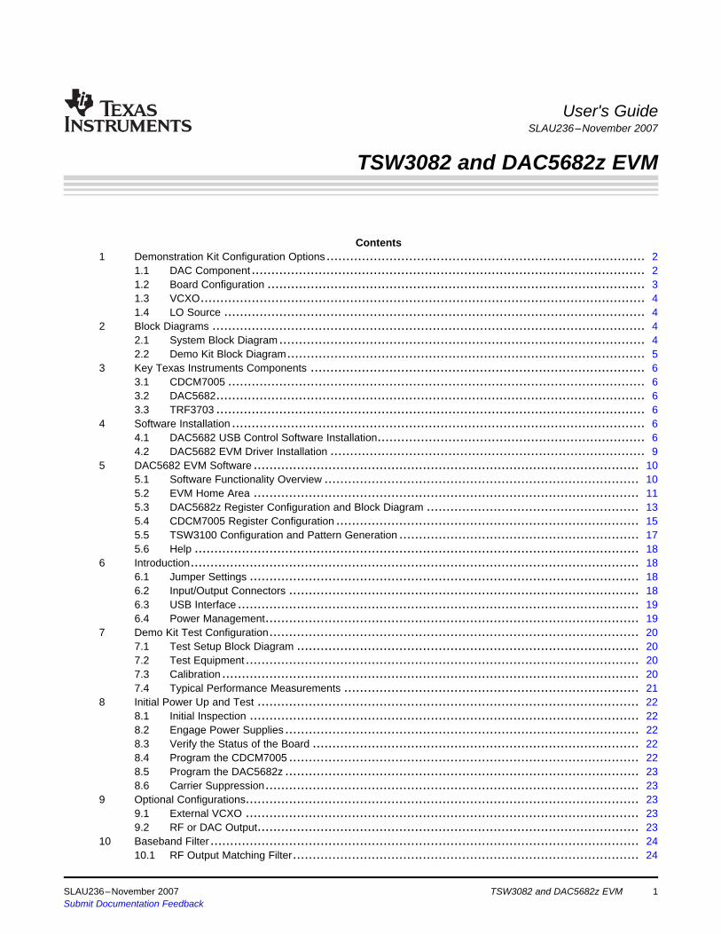
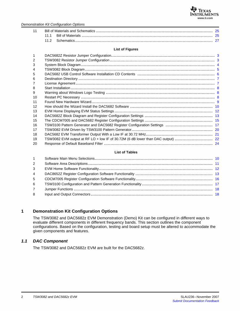
1.2 Board ConfigurationDemonstration Kit Configuration Options
The analog quadrature modulator requires a common-mode DC voltage of approximately 3.3V. In order touse the dc-offset adjustment capabilities of the DAC5682 for carrier suppression, it is imperative tomaintain a dc path from the DAC output to the modulator input. The common-mode voltage for themodulator is maintained with a passive resistor network that is designed to provide the proper operationpoint for the DAC5682 and the TRF3703 modulator. By design, in order to preserve the proper dc levels,the DAC coarse gain should be kept at the maximum (15), though deviation by a few steps is generallyacceptable with no degradation in performance.
The resistor network can be configured such that the DAC output is routed to a transformer which definesthe board as a DAC5682z EVM or routed to the TRF3703 which results in the TSW3082 EVM.
Figure 1. DAC5682Z Resistor Jumper Configuration
Figure 2. TSW3082 Resistor Jumper Configuration
SLAU236–November 2007 TSW3082 and DAC5682z EVM 3Submit Documentation Feedback
www.ti.com
1.3 VCXO
1.4 LO Source
2 Block Diagrams
2.1 System Block Diagram
Block Diagrams
The CDCM7005 requires a VCXO or external clock source to derive its output clock signals. The VCXO isat reference designator U6. This TSW3082 and DAC5682z EVM release does not have a VCXO andrequires an external clock source on SMA J6. The VCXO can be changed to operate the Demo Kit withdifferent clocking schemes for different modulation standards or for specific customer requirements. Usethe VCXO or external clock frequency to properly configure the CDCM7005 (see Section 2 of Figure 15).
These conventions are typically used:• WCDMA—derivatives of 61.44 MHz• GSM—derivatives of 52 MHz• CDMA2K—derivatives of 78.6432 MHz• WiMAX—derivatives of 112 MHz
The TSW3082 requires an external Local Oscillator (LO) source to drive the on board TRF3703-33modulator. This external LO input can be connected at SMA connector J23. The signal level of the LOsource should comply with the requirements in the TRF3703 data sheet (SLWS184), but typically an LOpower around 0 to 3 dBm is adequate.
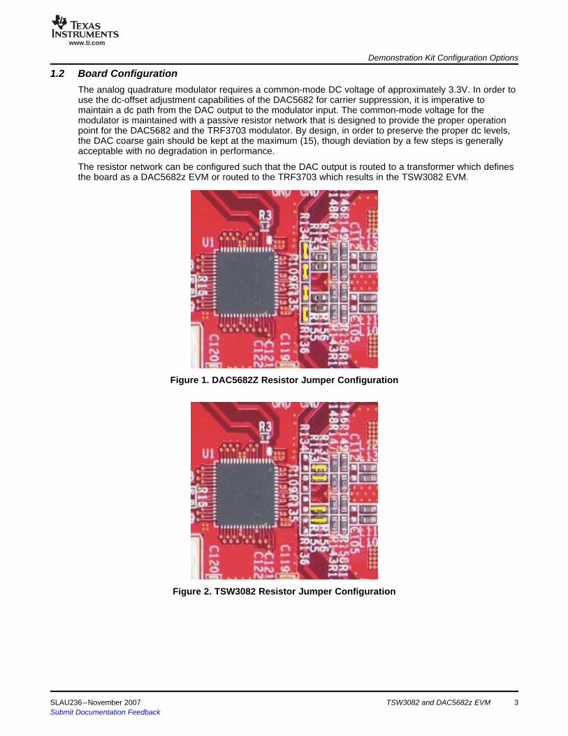
The basic radio system block diagram in Figure 3 demonstrates where the TSW3082 Demo Kit fits in theoverall transceiver. The dash-line box illustrates the components found on the TSW3082 Demo Kit board.
Figure 3. System Block Diagram
TSW3082 and DAC5682z EVM4 SLAU236–November 2007Submit Documentation Feedback

www.ti.com
2.2 Demo Kit Block DiagramBlock Diagrams
The basic Demo Kit block diagram is shown in Figure 4. The shaded boxes illustrate the key TexasInstruments components found on the TSW3082 Demo Kit board.
Figure 4. TSW3082 Block Diagram
SLAU236–November 2007 TSW3082 and DAC5682z EVM 5Submit Documentation Feedback

www.ti.com
3 Key Texas Instruments Components
3.1 CDCM7005
3.2 DAC5682
3.3 TRF3703
4 Software Installation
4.1 DAC5682 USB Control Software Installation
Key Texas Instruments Components
The CDCM7005 clock distribution chip is used to generate and synchronize the clock outputs to thesystem. The device has five outputs which can be either LVPECL or LVCMOS, and can be divided downby 1, 2, 3, 4, 6, 8, and 16. The divide by 16 can be replaced with a divide by 4 or 8 with a 90 degreephase shift. See the CDCM7005 data sheet (SCAS793) for more information.
The DAC5682 is a 16-bit interpolating dual digital-to-analog converter (DAC) with a high speed LVDS datainterface. The device incorporates a digital complex coarse mixer, independent differential offset control,and I/Q amplitude control. The device can be used with excellent results in baseband mode, low IF mode,as well as in high IF mode with an analog quadrature modulator. See the DAC5682 data sheet (SLLS853)for more information.
The TRF3703 is a direct upconversion (DUC) IQ modulator. This device accepts a differential inputvoltage quadrature signal at baseband or low IF frequencies and outputs a modulated RF signal based onthe LO drive frequency. See the TRF3703 data sheet (SLWS184) for more information.
The enclosed CD-ROM contains all of the necessary software needed for the host PC to control theDAC5682Zz and CDCM7005. The interface software is a Graphical User Interface (GUI) that can programall the registers in the CDCM7005 and the DAC5682z. Once the software is installed, the GUI isaccessible from the Start → All Programs → Texas Instruments DACs → DAC5682z EVM Control.
The installation CD contains the files and folders shown in Figure 5.
Figure 5. DAC5682 USB Control Software Installation CD Contents
1. Double-click the setup.exe file (Figure 5) to start the DAC5682z control software installation.2. The destination folder for the installed software displays (Figure 6). TI recommends you accept the
default folder location. Any necessary folders are created by the installation software, if they do not
6 TSW3082 and DAC5682z EVM SLAU236–November 2007Submit Documentation Feedback

www.ti.com
Software Installation
exist. Click Next.3. Select the I accept the License Agreement(s) option (Figure 7) and click Next.4. Click Next (Figure 8) to start the installation.5. Click Continue Anyway (Figure 9) to continue the installation.6. Click Restart (Figure 10) to finish the installation.
Figure 6. Destination Directory
Figure 7. License Agreement
SLAU236–November 2007 TSW3082 and DAC5682z EVM 7Submit Documentation Feedback

www.ti.com
Software Installation
Figure 8. Start Installation
Figure 9. Warning about Windows Logo Testing
Figure 10. Restart PC Necessary
TSW3082 and DAC5682z EVM8 SLAU236–November 2007Submit Documentation Feedback

www.ti.com
4.2 DAC5682 EVM Driver InstallationSoftware Installation
1. Once the PC has restarted, plug in the DAC5682z or TSW3082 EVM. This starts the driver installationprocess. The Found New Hardware Wizard (Figure 11) detects the DAC5682. When asked if Windowsshould connect to the Windows Update server to locate drivers, select the No, not this time option andclick the Next button.
2. When asked how do you want the wizard to install the software (Figure 12), select the Install thesoftware automatically (Recommended option.. Click Next.
3. Click Continue for the digital signature.4. The drivers were installed during the software installer and will be installed automatically. If asked to
overwrite newer drivers, click Yes.5. Click Finish to complete the driver installation.
Figure 11. Found New Hardware Wizard
SLAU236–November 2007 TSW3082 and DAC5682z EVM 9Submit Documentation Feedback

www.ti.com
5 DAC5682 EVM Software
5.1 Software Functionality Overview
DAC5682 EVM Software
Figure 12. How should the Wizard Install the DAC5682 Software
The DAC5682z EVM Control Software is started by accessing the Windows start → All Programs →Texas Instruments DACs cascading menus.
The DAC5682z EVM application helps you to:• Configure the DAC5682z and CDCM7005 registers.• Save and load these register settings using text files.• Visualize the data path through the DAC5682z• Download a pattern to a TSW3100 Pattern Generator System (link to TSW3100 EVM folder).
This section provides you an overview of the software settings and functionality for the entire DAC5682Graphical User Interface. The software has five groups of settings that help you modify the functionality ofthe active panels. You can switch between these settings by selecting one of the Menu items described inTable 1.
Table 1. Software Main Menu SelectionsMenu Item Top Panel Bottom Panel Section
Example ScreenFunctionality Reference
EVM Home EVM and DAC5682z serial not applicable Section 5.2information. Figure 13EVM communication status Table 3
DAC5682z DAC5682z Register Configuration DAC5682z data path under the Section 5.3Diagram current register settings Figure 14
Table 4Register Config DAC5682z Register Configuration CDCM7005 Register Section 5.4
Configuration Figure 15Table 5
10 TSW3082 and DAC5682z EVM SLAU236–November 2007Submit Documentation Feedback
www.ti.com
5.2 EVM Home Area
DAC5682 EVM Software
Table 1. Software Main Menu Selections (continued)Menu Item Top Panel Bottom Panel Section
Example ScreenFunctionality Reference
TSW3100 Config DAC5682z Register Configuration TSW3100 Configuration Section 5.5Pattern Generator display Figure 16
Table 6Help DAC5682z Register Configuration DAC5682z data path and help Section 5.6
window
The DAC5682z software interface controls are divided into areas. The functionality of these areas isdescribed in Section 5.2 through Section 5.6.
Table 2. Software Area DescriptionsArea DescriptionMenu Switch between the main functionality settings described in Table 1.DAC5682Z Home Displays DAC5682Z part serial information and EVM status.USB and Readback buttons Reset the USB port to begin a new data session. Disable DAC5682z read capabilities
(simulation mode).DAC5682z Register Table Displays DAC5682z register settings in binary and hexadecimal formats.DAC5682z Register Configuration Read/Write DAC5682z register configuration.CDCM7005 Register Configuration Write CDCM7005 register configuration (no read capability)DAC5682z Diagram Graphical representation of the DAC5682z data path under current register configuration.TSW3100 Configuration Controls TSW3100 pattern generation system (See TSW3100 User's Guide SLLU101 for
more information)Help Information about specific DAC5682z register configuration GUI controls
Figure 13 through Figure 16 displays some of the Menu software areas.
The EVM Home Area includes these GUI controls:• Menu—switches between the major functionality listed in Table 1 and displayed in Figure 13.• Home—displays DAC5682Z part information and EVM status.• USB/Readback—reset the USB port to begin a new data session. Disable DAC5682z read capabilities
(simulation mode).• DAC5682z Register Table—displays DAC5682Z register settings in binary and hexadecimal formats
(Figure 14 - Regs).
Note: The numbers on Figure 13 through Figure 16 correspond to the numbered graphical userinterface subareas (X), described in each table for the DAC5682z EVM softwarefunctionality.
SLAU236–November 2007 TSW3082 and DAC5682z EVM 11Submit Documentation Feedback

www.ti.com
DAC5682 EVM Software
Figure 13. EVM Home Displaying EVM Status Settings
Table 3. EVM Home Software FunctionalityInputSubarea Name DescriptionOutput
Menu Area (1)EVM Home Input DAC5682z EVM Home area - part number information and EVM status messagesDAC5682z Diagram Input DAC5682z Register Configuration and DAC5682z Diagram areasRegister Config Input . DAC5682z and CDCM7005 Register Configuration areasTSW3100 Config Input DAC5682z Register Configuration and TSW3100 Configuration areasHelp Input Help area
DAC5682z EVM Home Area (2)Functionality Output DAC deviceVersion Output Chip versionWafer number Output DAC5682z wafer numberColumn (x) Output DAC5682z column positionRow (y) Output DAC5682z row positionLot Number Output DAC5682z lot numberFab Output Fabrication facility where the DAC5682z was manufacturedEVM Serial Number Output Serial number for this EVMStatus Messages Output Displays the status of the communication session.
USB / Readback Area (3)Reset USB Port Input Begins a new USB session. Click this button if you see a status error message.Readback Input/Output Disables DAC5682z register reads (simulation mode)
DAC5682z Register Table Area (See Figure 14, Figure 15, and Figure 16)Displays the DAC5682z register configuration in binary and hexadecimal formats for allRegister Table Output menu settings.
TSW3082 and DAC5682z EVM12 SLAU236–November 2007Submit Documentation Feedback

www.ti.com
5.3 DAC5682z Register Configuration and Block DiagramDAC5682 EVM Software
Figure 14. DAC5682Z Block Diagram and Register Configuration Settings
Table 4. DAC8652Z Register Configuration Software FunctionalityInputSubarea Name Description of Functionality (GUI Setting)Output
PLL Settings (1)PLL Input/Output Phased-locked Loop (PLL) is bypassed (disabled)PLL Sleep Input/Output PLL is put into sleep mode (selected)PLL Lock Output Internal PLL is locked (Green)
PLL loop filter is pulled down to 0V (set).PLL Reset Input/Output Toggle to restart the PLL if an over-speed lock-up occurs.PLL clock output is one-half the PLL VCO frequency (2x).
VCO Frequency Input/Output Runs the VCO at twice the needed clock frequency to reduce phase noise for lower input clockrates.
PLL Gain (MHz/V) Input/Output Adjust the PLL Voltage Controlled Oscillator (VCO) gain.PLL Range (MHz) Input/Output Sets the PLL VCO frequency range.M value Input/Output M portion of the M/N divider of the PLL.
N portion of the M/N divider of the PLL. This value should be chosen to divide down the input CLKINN value Input/Output to maintain a maximum PFD of 160 MHz.
DLL Settings (2)Delay lock loop (DLL) is bypassed and LVDS data source provides correct setup and hold timingDLL Input/Output (disabled)
DLL Sleep Input/Output DLL is put into sleep mode (selected)DLL is restarted automatically when DLL settings change, so there is no need to press the DLLAuto-DLL Input restart control (selected).
DLL Lock Output Internal DLL is locked (Green)DLL restart Input/Output Restarts the DLL manually
SLAU236–November 2007 TSW3082 and DAC5682z EVM 13Submit Documentation Feedback
www.ti.com
DAC5682 EVM Software
Table 4. DAC8652Z Register Configuration Software Functionality (continued)InputSubarea Name Description of Functionality (GUI Setting)Output
DLL Delay (deg.) Input/Output Manually adjust the DLL delay ± from the DLL fixed current delay.DLL fixed current Adjusts the DLL delay line bias current. Used in conjunction with the DLL inv clock to selectInput/Outputdelay (ps/µA) appropriate delay range for a given DCLK frequency
Inverts the internal DLL clock to force convergence to a different solution. Used when the DLL delayDLL inv clock Input/Output adjustment has exceeded the limits of its range.
Input Settings (3)format Input/Output Select 2’s complement or offset binary format.reverse bus Input/Output Reverses the LVDS input data bus so that the MSB to LSB order is swapped (enabled)swap data Input/Output A/B data paths are swapped prior to routing to the DACA and DACB outputs (enabled)same data Input/Output Data routed to DACA is also routed to DACB (enabled)
Sets the FIFO’s output pointer location, allowing the input pointer to be shifted –4 to +3 positionsFIFO offset Input/Output upon SYNC. Default offset is 0 and is updated upon each sync event.
Digital Settings (4)digital logic Input/Output Uses the interpolation filters (enabled)interpolation Input/Output Selects the interpolation rate.
Determines the mode of FIR0 and CMIX0 blocks. Since CMIX0 is located between FIR0 and FIR1,CM0 mode Input/Output its output is half-rate. Settings apply to both A and B channels.CM1 mode Input/Output Determines the mode of FIR1 and final CMIX1 blocks. Settings apply to both A and B channels.
DAC data delay adjustment (0–3 periods of the DAC clock). Used to adjust system level outputdigital delay Input/Output timing. The same delay is applied to both DACA and DACB data paths.Changes the number of buffers that the input clock goes through. This allows some adjustment ofclock delay Input/Output the setup/hold of the handoff between the receivers and the digital section.
DAC Settings (5)DAC mode Input/Output Selects dual DAC mode or single DAC mode. Used to select input interleaved data (dual DAC).DACA Sleep Input/Output DACA is put into sleep mode (selected)
DACB is put into sleep mode (selected). DACB is not automatically set into sleep mode whenDACB Sleep Input/Output configured for single DAC mode. Use this control with single DAC mode to get the lowest power
configuration for DACA output only.DACA Gain Input/Output Scales the DACA output current in 16 equal steps.DACB Gain Input/Output Scales the DACB output current in 16 equal steps.
Offset A and Offset B values are summed into the DACA and DACB data paths (enabled). ProvidesOffset Input/Output a system-level offset adjustment capability that is independent of the input data.Transfers the Offset A and Offset B values to the registers used in the DACA and DACB offsetoffset sync Input/Output calculations. This control is enabled automatically for any change in the Offset A or Offset B values.
Offset A Input/Output Offset adjustment value for the A data path.Offset B Input/Output Offset adjustment value for the B data path.
95 kHz low pass filter corner on the DACA current source bias (enabled). Uses a 472 Hz filterDAC A LPF Input/Output corner (disabled).95 kHz low pass filter corner on the DACB current source bias (enabled). Uses a 472 Hz filterDAC B LPF Input/Output corner (disabled).
Error Settings (6)SLFST Error Input/Output Masks out SLFTST Errors.FIFO Error Input/Output Masks out FIFO Errors.Setup/Hold Error Input/Output Masks out Setup/Hold Errors.SLFST error reset Input/Output Asserted when the Digital Self Test (SLFTST) fails. Clear to reset a SLFST error.
Asserted when the FIFO pointers overrun each other, causing a sample to be missed. Clear to resetFIFO error reset Input/Output a FIFO error.Any received data pattern other than 0xAAAA or 0x5555 causes this bit to be set. Clear to reset aSetup/Hold error reset Input/Output Setup/Hold error.
SDO Input/Output Selects the signal polarity on the SDO pin (normal or inverted)
14 TSW3082 and DAC5682z EVM SLAU236–November 2007Submit Documentation Feedback

www.ti.com
5.4 CDCM7005 Register Configuration
DAC5682 EVM Software
Table 4. DAC8652Z Register Configuration Software Functionality (continued)InputSubarea Name Description of Functionality (GUI Setting)Output
SYNC Settings (7)serial interface Input/Output Selects 3-pin or 4-pin serial interface mode.
Selects the synchronization signal source. If soft sync is selected the software sync control is usedsync source Input/Output as the only synchronization input and the LVDS external SYNC input pins (hard sync) are ignored.Substitute for the LVDS external SYNC input pins for both synchronization and transmit enablesoftware sync Input/Output control.
hold sync Input/Output Enables the sync to the FIFO output HOLD block.clk div sync Input/Output Enables the clock divider sync.FIFO sync Input/Output Enables the FIFO offset sync.self test Input/Output Enables a Digital Self Test (SLFTST) of the core logic.FA002 Input/Output Keep disabled. Used only for factory test purposes.Fuse A Input/Output Keep disabled. Used only for factory test purposes.Fuse B Input/Output Keep disabled. Used only for factory test purposes.ATEST Input/Output Keep disabled. Used only for factory test purposes.
SEND/SAVE Button Settings (8)Send All Input Writes all registers to the DAC5682z device.
Reads all registers from the DAC5682z device. It is rarely necessary to use this as the registers areRead All Input read every time a DAC5682z control changes.Loads a DAC5682z register configuration from a text file. Files need to consist of a single columnLoad Regs Input with the register values in hexadecimal format.
Save Regs Input Saves a DAC5682z register configuration to a text file.
Figure 15. The CDCM7005 and DAC5682 Register Configuration Settings
SLAU236–November 2007 TSW3082 and DAC5682z EVM 15Submit Documentation Feedback

www.ti.com
DAC5682 EVM Software
Table 5. CDCM7005 Register Configuration Software FunctionalityInputSubarea Name DescriptionOutput
General Settings (1)Output Settings Input Switches the display between the CDCM7005 output settings and advanced settings.
Select Buffer Mode when there is no VCXO installed or the VCXO is enabled. In this case theCDCM7005 Operation Input CDCM7005 operates as a buffer. Select PLL Mode when a VCXO is being used by the
CDCM7005.
PLL Settings (2)(Auto) M and N divider values are calculated automatically based on Reference and VCXOM & N Selection Input frequencies.
Ref. Freq. (MHz) Input Frequency of the reference oscillator given to the CDCM7005.VCXO Freq. (MHz) Input Frequency of the VCXO used.M Divider Input/Output M divider value.N Divider Input/Output N divider value.FB_MUX Input/Output Feedback MUX select.Phase Shift Input Phase shift select.
Output frequency of the CDCM7005 based on the Reference and VCXO frequencies, and M andOutput Freq (MHz) Output N values. If Output Freq differs from VCXO Freq, Output Freq displays using a red text.
Output Settings (3)Y0-Y4 Dividers Input Selects the output dividers of the CDCM7005 outputs.Y0-Y4 Levels Input Selects between CMOS or LVPECL levels of the CDCM7005 outputs.Y0-Y4 States Input Selects the operating state of the CDCM7005 outputs.
SEND/SAVE Button Settings (4)Send All Input Writes all registers to the DCDM7005 device.
Loads a DCDM7005 register configuration from a text file. Files need to consist of a singleLoad Regs Input column with the register values in hexadecimal format.Save Regs Input Saves a DCDM7005 register configuration to a text file.
Advanced Settings (not shown)Input CDCM7005 advanced registers. See the CDCM7005 data sheet (SCAS793) for moreAdvanced Registers information about these registers.
16 TSW3082 and DAC5682z EVM SLAU236–November 2007Submit Documentation Feedback
www.ti.com
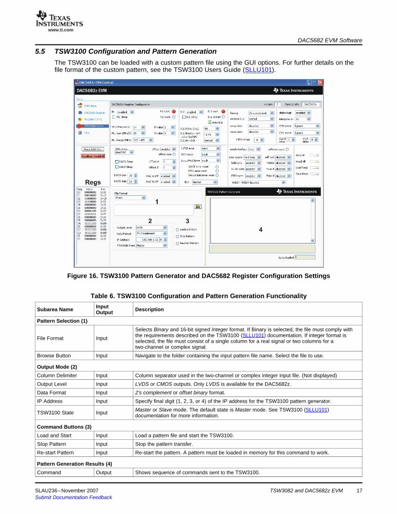
5.5 TSW3100 Configuration and Pattern GenerationDAC5682 EVM Software
The TSW3100 can be loaded with a custom pattern file using the GUI options. For further details on thefile format of the custom pattern, see the TSW3100 Users Guide (SLLU101).
Figure 16. TSW3100 Pattern Generator and DAC5682 Register Configuration Settings
Table 6. TSW3100 Configuration and Pattern Generation FunctionalityInputSubarea Name DescriptionOutput
Pattern Selection (1)Selects Binary and 16-bit signed Integer format. If Binary is selected, the file must comply withthe requirements described on the TSW3100 (SLLU101) documentation. If integer format isFile Format Input selected, the file must consist of a single column for a real signal or two columns for atwo-channel or complex signal.
Browse Button Input Navigate to the folder containing the input pattern file name. Select the file to use.
Output Mode (2)Column Delimiter Input Column separator used in the two-channel or complex integer input file. (Not displayed)Output Level Input LVDS or CMOS outputs. Only LVDS is available for the DAC5682z.Data Format Input 2's complement or offset binary format.IP Address Input Specify final digit (1, 2, 3, or 4) of the IP address for the TSW3100 pattern generator.
Master or Slave mode. The default state is Master mode. See TSW3100 (SLLU101)TSW3100 State Input documentation for more information.
Command Buttons (3)Load and Start Input Load a pattern file and start the TSW3100.Stop Pattern Input Stop the pattern transfer.Re-start Pattern Input Re-start the pattern. A pattern must be loaded in memory for this command to work.
Pattern Generation Results (4)Command Output Shows sequence of commands sent to the TSW3100.
SLAU236–November 2007 TSW3082 and DAC5682z EVM 17Submit Documentation Feedback

www.ti.com
5.6 Help
6 Introduction
6.1 Jumper Settings
6.2 Input/Output Connectors
Introduction
Table 6. TSW3100 Configuration and Pattern Generation Functionality (continued)InputSubarea Name DescriptionOutput
Status Output Status of the TSW3100 transaction.Bytes loaded Output Number of bytes loaded to the TSW3100.
When you select the the Help menu item, the DAC5682 Diagram screen (Figure 14) and a detached,pop-up Help text window display. As you move the cursor over the DAC5682 Diagram GUI controls, thecontext-sensitive help text changes in the pop-up window.
The DAC5682z EVM provides a robust and flexible evaluation system for the DAC5682z. The EVMincludes (in addition to the DAC5682z) a CDCM7005 for clock distribution and an optional TRF3703quadrature modulator path for RF measurements. For a complete hardware description, please consultthe schematics and layout sections at the end of this guide. See the DAC5682 (SLLS853), CDCM7005(SCAS793), and TRF3703 (SLWS184) data sheets for more information.
The DAC5682z uses onboard jumpers to help you modify the DAC5682z board configuration. Table 7explains the functionality of these jumpers.
Table 7. Jumper FunctionsJumper Label Function Condition Default
JP8 EXTLO Internal (GND) or external (3.3V) voltage reference GND Pin 2-3JP10 VFUSE Factory use only. Connect to 1.8VDD for normal operation. 1.8 VDD Pin 1-2JP12 CDC_PD Low active power down of CDCM7005 3.3 VCLK Pin 1-2JP13 VCXOB Choose internal VCXO or external VCXO INB External VCXO Pin 2-3JP14 VCXO_P Choose internal VCXO or external VCXO positive input External VCXO Pin 2-3JP15 VCXO_N Choose CDCM7005 or external VBB CDCM7005 Pin 1-2JP16 REF_CLK Choose internal 10-MHz ref or external ref Internal Ref Pin 2-3JP17 +3.3V_IN Main or TP3 3.3 voltage source for CDCM7005 and USB Main Pin 1-2JP19 +3.3VCLK VCXO power down 3.3 VCLK Pin 1-2
Table 8 lists the input and output connectors.
Table 8. Input and Output ConnectorsReference Label Connector Type DescriptionDesignator
J1 IOUTB2 SMA DACB transformer output. Optional IOUTB2 output.J2 IOUTB1 SMA Optional IOUTB1 output.J3 IOUTA2 SMA DACA transformer output. Optional IOUTA2 output.J4 IOUTA1 SMA Optional IOUTA1 output.J5 SEMTEK Input LVDS data to DAC682z. Output clock to data source.J6 EXT_VCXO_P SMA External main clock input.J7 EXT_VCXO_N SMA External VCXO negative connection. Not required.
18 TSW3082 and DAC5682z EVM SLAU236–November 2007Submit Documentation Feedback

www.ti.com
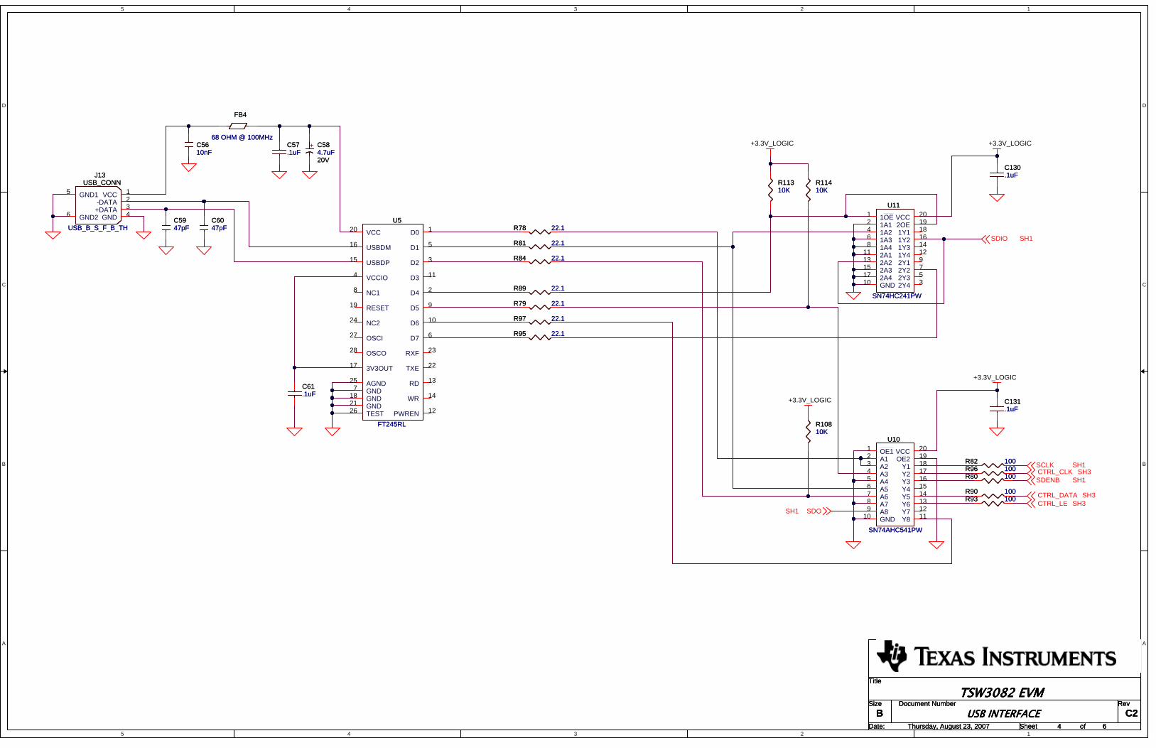
6.3 USB Interface
6.4 Power Management
Introduction
Table 8. Input and Output Connectors (continued)Reference Label Connector Type DescriptionDesignator
J8 Y2A_CLK SMA Optional CDCM7005 clock output.J9 EXT_REF_CLK SMA External reference clock input.J10 Y2B_CLK SMA Optional CDCM7005 clock output.J13 USB_CONN USB USB connector for software communication.
J14/J15 +1.8V_IN Banana Plug +1.8V connection pair.J16 RFOUT SMA RF output from TRF3703.
J17/J18 +3.3V_IN Banana Plug +3.3V connection pair.J19/J20 +5VA_IN Banana Plug +5V connection pair. Required only for RF measurements.
J23 RF_LO_IN SMA TRF3703 LO source input.
The DAC5682z EVM has a 4-pin USB port connector that interfaces to a USB 1.1 (or later) compliant USBport. You can program the CDCM7005 and DAC5682z using this USB port.
The DAC5682z EVM requires 1.8 V and 3.3 V supplies for normal operation. An additional 5 V supply isrequired supply power to the TRF3073 for RF measurements.
SLAU236–November 2007 TSW3082 and DAC5682z EVM 19Submit Documentation Feedback

www.ti.com
7 Demo Kit Test Configuration
7.1 Test Setup Block Diagram
7.2 Test Equipment
7.3 Calibration
Demo Kit Test Configuration
The test setup for the TSW3082 and DAC5682z EVM is shown in Figure 17. This setup shows theTSW3100 pattern generator supplying an LVDS signal to the TSW3082/DAC5682 EVM.
Figure 17. TSW3082 EVM Driven by TSW3100 Pattern Generator
This test equipment is required for testing the TSW3082 and DAC5682 EVM. Other equipment may besubstituted, however results may vary due to instrument limitations.• Power supplies—1.8 V (DAC digital), 3.3 V (DAC analog), and 5 V (RF modulator)• Spectrum Analyzer—Rhode & Schwarz FSU, FSQ, or equivalent. This is necessary to measure the
noise floor ACPR greater than 70 dBm with the noise correction option.• Pattern generator—TSW3100 using LVDS mode, or some other LVDS capable generator.• Oscilloscope—probe clock and data lines for troubleshooting.• Digital volt meter—verify signal levels.
To measure the proper output power, the insertion loss of the analyzer cable must be calibrated. Measurea calibrated 0 dBm source to see how much loss is in the cable at the frequency of interest.
TSW3082 and DAC5682z EVM20 SLAU236–November 2007Submit Documentation Feedback

www.ti.com
7.4 Typical Performance Measurements
Ref -12 dBm Att 10 dB*
*
*
A
NOR
RBW 30 kHz
VBW 300 kHz
SWT 2 s*
Center 30.72 MHz Span 25.5 MHz2.55 MHz/
*1 RM
CLRWR
-110
-100
-90
-80
-70
-60
-50
-40
-30
-20
Tx Channel W-CDMA 3GPP FWD
Bandwidth 3.84 MHz Power -8.02 dBm
Adjacent Channel
Bandwidth 3.84 MHz Lower -81.73 dBSpacing 5 MHz Upper -81.65 dB
Alternate Channel
Bandwidth 3.84 MHz Lower -82.95 dBSpacing 10 MHz Upper -82.74 dB
Demo Kit Test Configuration
The DAC5682 EVM measurements at the transformer outputs J1 and J3 (modulator is not used) will havebetter performance than the RF output. The RF output is typically limited by the performance of the RFparts. In this case the DAC output at 0 IF or low IF is several dB better than the noise floor of themodulator output at J16.
Figure 18. DAC5682 EVM Transformer Output With a Low IF at 30.72 MHz
SLAU236–November 2007 TSW3082 and DAC5682z EVM 21Submit Documentation Feedback

www.ti.com
A
Ref -13.2 dBm Att 5 dB*
*
*
*1 RM
CLRWR
RBW 30 kHz
VBW 300 kHz
SWT 2 s
NOR
*
Center 2.53072 GHz Span 25.5 MHz2.55 MHz/
-110
-100
-90
-80
-70
-60
-50
-40
-30
-20
Tx Channel W-CDMA 3GPP FWD
Bandwidth 3.84 MHz Power -8.95 dBm
Adjacent Channel
Bandwidth 3.84 MHz Lower -75.79 dBSpacing 5 MHz Upper -75.42 dB
Alternate Channel
Bandwidth 3.84 MHz Lower -78.44 dBSpacing 10 MHz Upper -77.21 dB
8 Initial Power Up and Test
8.1 Initial Inspection
8.2 Engage Power Supplies
8.3 Verify the Status of the Board
8.4 Program the CDCM7005
Initial Power Up and Test
Figure 19. TSW3082 EVM output at RF LO + low IF of 30.72M (6 dB lower than DAC output)
This section outlines the basic power application and test procedure to ensure the EVM is in anoperational state.
Inspect the board to determine which VCXO resides on the board. This is useful when programming theCDCM7005 to lock the DAC clock to the reference.
Engage the power supplies for 1.8 V, 3.3 V, and 5 V. Ensure that each supply is not drawing more than1 A of current. Typically the 1.8 V will be less than 1 A, 3.3 V less than 200 mA, and 5 V less than 0.5 A.
The DAC software detects if the USB port is active and if it is capable of reading the serial number fromthe EVM. This determines if the communication between the board and PC is correct. The EVM Homemenu (Figure 13 and Table 3) of the DAC8652z GUI software provides this status information.
Navigate to the Register Config menu (Figure 15 and Table 5). Program the CDCM7005 registers asnecessary. Typically a reg.cdcm7005 register file is provided to initialize the default settings. Load thisregister file using the section 4 (SEND/SAVE Button Settings) controls described in Table 5 .
TSW3082 and DAC5682z EVM22 SLAU236–November 2007Submit Documentation Feedback

www.ti.com
8.5 Program the DAC5682z
8.6 Carrier Suppression
9 Optional Configurations
9.1 External VCXO
9.2 RF or DAC Output
Optional Configurations
Navigate to the DAC5682 Diagram menu (Figure 14 and Table 4 ). Adjust the register settings as desired.Typically a reg.dac5682 register file provides a set of test register values. Load this register file using thesection 8 (SEND/SAVE Button Settings) controls described in Table 4 .
Carrier feed through is dependent on the DC offset between I and Q paths. There are registers in the DACthat provided some digital DC correction. A feedback path is necessary to perform this correction. Contactthe TI factory applications team for more details.
It is possible to configure the TSW3082 and DAC5682 EVM to use an external VCXO for applicationflexibility. J13 and J14 may be used in position 2-3 to select an external VCXO or clock signal.
The board is populated with the TRF3703 modulator. If the board is configured for DAC output, themodulator is not used and 5 V power is unnecessary. The DAC outputs in this setup are J1 and J3.
If the board is configured for RF output, the 5 V must be used to power the modulator. The resistor path atthe output of the DAC must be changed to pass the signal to the modulator instead of to the transformers.In this case an external LO must be provided on J23 and the RF output is present at J16.
SLAU236–November 2007 TSW3082 and DAC5682z EVM 23Submit Documentation Feedback

www.ti.com
10 Baseband Filter
10.1 RF Output Matching Filter
Baseband Filter
The TSW3082 EVM is configured with enough pads to provide a customer a specific 5th-order differentialpassive LC filter. By default, it is only populated with a simple LC low pass filter to attenuate the higherclock harmonics. The 3 dB corner of this filter is approximately 300 MHz.
Figure 20. Response of Default Baseband Filter
The TSW3082 RF output provides a pi pad network on the modulator output to provide some matching orfiltering if desired. In its default state the pad is not used and a series cap is used on the RF output.
TSW3082 and DAC5682z EVM24 SLAU236–November 2007Submit Documentation Feedback

www.ti.com
11 Bill of Materials and Schematics
11.1 Bill of Materials
Bill of Materials and Schematics
This section contains the bill of materials and schematics for the DAC5682 and TSW3083 EVM.
Qty Part Reference Value PCB Footprint Mfr_Name Mfr_Part_Number Note
12 C1 C2 C5 C8 C56 C70 0.01 µF 0603 Panasonic ECJ-1VB1C103KC76 C79 C84 C87C121 C124
1 C3 0.15 µF 0402 Murata GRM36X5R154K10H520
6 C4 C29 C48 C104 1000 pF 0402 Panasonic ECJ-0EB1E102KC106 C127
38 C6 C7 C9–C15 C17 0.1 µF 0402 Panasonic ECJ-0EB1C104KC18 C20 C23–C25C27 C33 C38–C47C50–C52 C57 C61C94 C95 C107 C114C130 C131
16 C16 C21 C32 C36 C53 10 µF tant_a Kermet T494A106M016ASC54 C71 C74 C80 C82C88 C93 C97 C98C120 C126
1 C22 560 pF 0402 Panasonic ECJ-0EB1H561K
2 C31 C113 100 pF 0402 Panasonic ECJ-0EB1E101K
8 C34 C69 C75 C78 C83 1 µF 0603 Panasonic ECJ-1V41E105MC86 C122 C125
1 C35 0.47 µF 0603 Murata GRM188R71C474KA88D
3 C49 C128 C129 0.01 µF 0402 Panasonic ECJ-0EB1E103K
3 C58 C108 C115 4.7 µF tant_a AVX TAJA475K020R
2 C59 C60 47 pF 0603 Panasonic ECJ-1VC1H470J
7 C72 C77 C81 C85 C89 47 µF tant_b Kemet T494B476M010ASC119 C123
0 C73 C100 C101 C116 4.7 pF 0603 Panasonic ECJ-1VC1H047C_DNI DNI
2 C99 C109 3.3 pF 0402 Murata GRM1555C1H3R3CZ01D
2 C102 C103 22 pF 0402 Panasonic ECJ-0EC1H220J
0 C105 C112 2.2 pF 0603 AVX 06035A2R2CAT2A_DNI DNI
2 C110 C111 2.7 pF 0603 AVX 06035A2R7CAT2A
0 C117 C118 0.01 uF 0402 Panasonic ECJ-0EB1E103K_DNI DNI
3 D1-D3 LED green LED_0805 Panasonic LNJ306G5UUX
3 D12–D14 MBRB2515L DIODE_MBRB2515L ON MBRB2515LT4GSemiconductor
13 FB1–FB13 68 Ω at 100 MHz 1206 Panasonic EXC-ML32A680U
4 J1–J4 SMA_PCB_THVT SMA_THVT_312x312 Johnson 142-0701-201Components
7 J6–J10 J16 J23 SMA_END_JACK_RN SMA_SMEL_218x247_096 Johnson 142-0761-801D Components
1 J13 USB_B_S_F_B_TH CON_THRT_USB_B_F SAMTEC USB-B-S-F-B-TH
3 J14 J17 J20 BANANA_JACK_RED CON_THVT_BANANA_JACK_250 SPC Technology 845-RDIA
3 J15 J18 J19 BANANA_JACK_BLK CON_THVT_BANANA_JACK_250 SPC Technology 845-BDIA
1 J5 ASP-122952-01 CON_SMVT_160POS_ASP_1229 SAMTEC ASP-122952-0152
4 JP8 JP13 JP14 JP16 Jumper_1x3_100_430L HDR_THVT_1x3_100_M SAMTEC HMTSW-103-07-G-S-.230 (SHUNT 2-3)
4 JP10 JP12 JP15 JP17 Jumper_1x3_100_430L HDR_THVT_1x3_100_M SAMTEC HMTSW-103-07-G-S-.230 (SHUNT 1-2)
1 JP19 Jumper_1x2_100_430L HDR_THVT_1x2_100_M SAMTEC HMTSW-102-07-G-S-.230
0 L6 L7 56 nH IND_0603 Panasonic ELJ-RE56NJF3_DNI DNI
4 L8 L9 L14 L15 10 nH IND_0603 Coilcraft 0603CS-10NXLU
4 L10–L13 68 nH 0603 Coilcraft 0603CS-68NXJL
0 R1 R2 R4 R5 R12 R14 1 KΩ 0402 Panasonic ERJ-2RKF1001X_DNI DNIR17 R19
SLAU236–November 2007 TSW3082 and DAC5682z EVM 25Submit Documentation Feedback

www.ti.com
Bill of Materials and Schematics
Qty Part Reference Value PCB Footprint Mfr_Name Mfr_Part_Number Note
10 R3 R7 R13 R21 R26 100 Ω 0402 Panasonic ERJ-2RKF1000XR80 R82 R90 R93 R96
0 R6 R9 R15 R20 R23 0 0603 Panasonic ERJ-3GEY0R00V_DNI DNIR27 R109 R134–R136
5 R8 R22 R44 R49 R62 0 0402 Panasonic ERJ-2GE0R00X
1 R10 93.1 Ω 0402 Panasonic ERJ-2RKF93R1X
0 R11 R24 R132 R133 60.4 Ω 0603 Yageo RC0603FR-0760R4L_DNI DNI
0 R16 100 Ω 0603 Panasonic ERJ-3EKF1000V_DNI DNI
1 R18 953 Ω 0402 Panasonic ERJ-2RKF9530X
1 R25 1 KΩ 0402 Panasonic ERJ-2RKF1001X
3 R28–R30 750 Ω 0402 Panasonic ERJ-2RKF7500X
8 R31–R34 R42 R43 130 Ω 0402 Panasonic ERJ-2RKF1300XR66 R67
8 R36–R39 R46 R47 82.5 Ω 0402 Panasonic ERJ-2RKF82R5XR69 R70
2 R40 R116 150 Ω 0402 Panasonic ERJ-2RKF1500X
2 R41 R150 90.9 Ω 0603 Panasonic ERJ-3EKF90R9V
0 R45 R51 R122 R123 0 0402 Panasonic ERJ-2GE0R00X_DNI DNI
0 R48 R54 130 Ω 0402 Panasonic ERJ-2RKF1300X_DNI DNI
9 R50 R56 R78 R79 R81 22.1 Ω 0402 Panasonic ERJ-2RKF22R1XR84 R89 R95 R97
0 R52 R57 R110 R111 150 Ω 0402 Panasonic ERJ-2RKF1500X_DNI DNI
0 R53 R58 82.5 Ω 0402 Panasonic ERJ-2RKF82R5X_DNI DNI
0 R55 49.9 Ω 0402 Panasonic ERJ-2RKF49R9X_DNI DNI
7 R59–R61 R64 R108 10 KΩ 0402 Panasonic ERJ-2RKF1002XR113 R114
1 R63 162 Ω 0402 Panasonic ERJ-2RKF1620X
1 R65 4.75 KΩ 0402 Panasonic ERJ-2RKF4751X
1 R92 100 Ω 0603 Panasonic ERJ-3EKF1000V
14 R137 R140–R142 0 0603 Panasonic ERJ-3GEY0R00VR145 R153 R155 R156R159–R164
4 R138 R151 R152 R154 60.4 Ω 0603 Yageo RC0603FR-0760R4L
1 R139 49.9 Ω 0402 Panasonic ERJ-2RKF49R9X
4 R143 R144 R147 R148 634 Ω 0603 Yageo RC0603FR-07634RL
4 R146 R149 R157 R158 115 Ω 0603 Yageo RC0603FR-07115RL
1 SW1 SW RESET SW_SMVT_RESET C&K KT11P3JM
2 T1 T2 ADT4-1T TFMR_6_250x340_100 Mini-Circuits ADT4-1T
8 TP1-TP8 Testloop_Black TP_THVT_060_RND Components TP-105-01-00Corporation
1 U1 DAC5682Z QFN_64_360x360_0p50mm_pwrp Texas Instruments DAC5682Zad
1 U2 CDCM7005 QFN_48_281x281_0p50mm_pwrp Texas Instruments CDCM7005RGZTad
1 U3 OSC-VECTRON OSC_4_SM_460x386 Vectron VTD3-J0BC-10M000
1 U5 FT245RL SSOP_28_413x220_26 FTDI Chip FT245RL
0 U6 2115–491.52 MHZ VCXO_6 Toyocom TCO-2111-491.52_DNI DNI
1 U8 TRF3703-33 QFN_24_163x163_0p50mm_pwrp Texas Instruments TRF3703-33IRGETad
1 U10 SN74AHC541PW TSSOP_20_260x177_26 Texas Instruments SN74AHC541PW
1 U11 SN74HC241PW TSSOP_20_260x177_26 Texas Instruments SN74HC241PW
4 Z_SCREW1– SCREW PANHEAD Building Fasteners PMS 440 0038 PH SCREW FORZ_SCREW4 4-40 x 3/8 STANDOFF
8 Z_SH-H1–Z_SH-H6 SHUNT-HEADER Keltron MJ-5.97-G SHUNT FORZ_SH-H9–Z_SH-H10 HEADER
4 Z_STANDOFF1– STANDOFF ALUM Keystone 2203 STANDOFFZ_STANDOFF4 HEX 4-40 x .500
TSW3082 and DAC5682z EVM26 SLAU236–November 2007Submit Documentation Feedback

www.ti.com
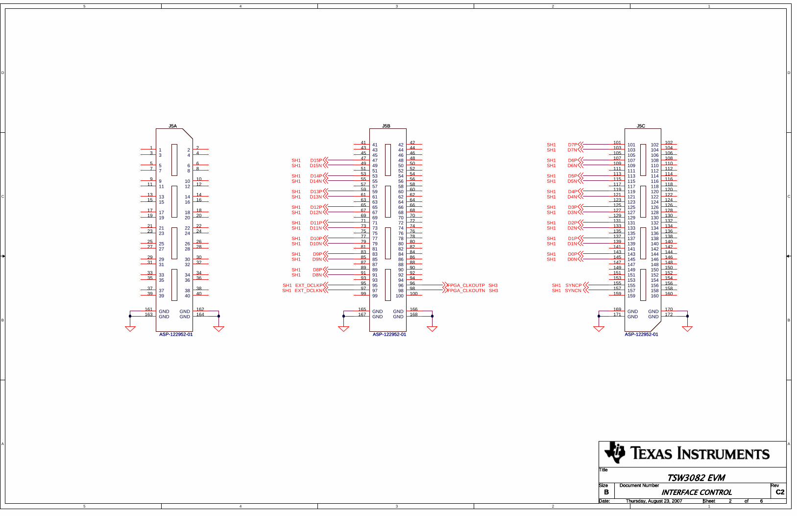
11.2 Schematics
Bill of Materials and Schematics
The TSW3082 and DAC5682 schematics are attached. These two EVMs share the same schematic witha different bill of materials.
SLAU236–November 2007 TSW3082 and DAC5682z EVM 27Submit Documentation Feedback
EVALUATION BOARD/KIT IMPORTANT NOTICETexas Instruments (TI) provides the enclosed product(s) under the following conditions:This evaluation board/kit is intended for use for ENGINEERING DEVELOPMENT, DEMONSTRATION, OR EVALUATION PURPOSESONLY and is not considered by TI to be a finished end-product fit for general consumer use. Persons handling the product(s) must haveelectronics training and observe good engineering practice standards. As such, the goods being provided are not intended to be completein terms of required design-, marketing-, and/or manufacturing-related protective considerations, including product safety and environmentalmeasures typically found in end products that incorporate such semiconductor components or circuit boards. This evaluation board/kit doesnot fall within the scope of the European Union directives regarding electromagnetic compatibility, restricted substances (RoHS), recycling(WEEE), FCC, CE or UL, and therefore may not meet the technical requirements of these directives or other related directives.Should this evaluation board/kit not meet the specifications indicated in the User’s Guide, the board/kit may be returned within 30 days fromthe date of delivery for a full refund. THE FOREGOING WARRANTY IS THE EXCLUSIVE WARRANTY MADE BY SELLER TO BUYERAND IS IN LIEU OF ALL OTHER WARRANTIES, EXPRESSED, IMPLIED, OR STATUTORY, INCLUDING ANY WARRANTY OFMERCHANTABILITY OR FITNESS FOR ANY PARTICULAR PURPOSE.The user assumes all responsibility and liability for proper and safe handling of the goods. Further, the user indemnifies TI from all claimsarising from the handling or use of the goods. Due to the open construction of the product, it is the user’s responsibility to take any and allappropriate precautions with regard to electrostatic discharge.EXCEPT TO THE EXTENT OF THE INDEMNITY SET FORTH ABOVE, NEITHER PARTY SHALL BE LIABLE TO THE OTHER FOR ANYINDIRECT, SPECIAL, INCIDENTAL, OR CONSEQUENTIAL DAMAGES.TI currently deals with a variety of customers for products, and therefore our arrangement with the user is not exclusive.TI assumes no liability for applications assistance, customer product design, software performance, or infringement of patents orservices described herein.Please read the User’s Guide and, specifically, the Warnings and Restrictions notice in the User’s Guide prior to handling the product. Thisnotice contains important safety information about temperatures and voltages. For additional information on TI’s environmental and/orsafety programs, please contact the TI application engineer or visit www.ti.com/esh.No license is granted under any patent right or other intellectual property right of TI covering or relating to any machine, process, orcombination in which such TI products or services might be or are used.
FCC WarningThis evaluation board/kit is intended for use for ENGINEERING DEVELOPMENT, DEMONSTRATION, OR EVALUATION PURPOSESONLY and is not considered by TI to be a finished end-product fit for general consumer use. It generates, uses, and can radiate radiofrequency energy and has not been tested for compliance with the limits of computing devices pursuant to part 15 of FCC rules, which aredesigned to provide reasonable protection against radio frequency interference. Operation of this equipment in other environments maycause interference with radio communications, in which case the user at his own expense will be required to take whatever measures maybe required to correct this interference.
Mailing Address: Texas Instruments, Post Office Box 655303, Dallas, Texas 75265Copyright © 2007, Texas Instruments Incorporated
EVM WARNINGS AND RESTRICTIONSIt is important to operate this EVM within the input voltage range of 1.8 V to 5.0 V and the output voltage range of 0.0 V to 3.3 V.Exceeding the specified input range may cause unexpected operation and/or irreversible damage to the EVM. If there are questionsconcerning the input range, please contact a TI field representative prior to connecting the input power.Applying loads outside of the specified output range may result in unintended operation and/or possible permanent damage to the EVM.Please consult the EVM User's Guide prior to connecting any load to the EVM output. If there is uncertainty as to the load specification,please contact a TI field representative.During normal operation, some circuit components may have case temperatures greater than 60° C. The EVM is designed to operateproperly with certain components above 60° C as long as the input and output ranges are maintained. These components include but arenot limited to linear regulators, switching transistors, pass transistors, and current sense resistors. These types of devices can be identifiedusing the EVM schematic located in the EVM User's Guide. When placing measurement probes near these devices during operation,please be aware that these devices may be very warm to the touch.
Mailing Address: Texas Instruments, Post Office Box 655303, Dallas, Texas 75265Copyright © 2007, Texas Instruments Incorporated

5
5
4
4
3
3
2
2
1
1
D D
C C
B B
A A
+3.3VA +1.8VD
+1.8VD1
+3.3VA
+3.3VA
+1.8VD1
+1.8VD
+3.3VA
+3.3VA
+3.3VA
+3.3VA
+3.3VA
+3.3VA
+3.3VA
+1.8VCLK
+1.8VD
+1.8VD
+1.8VCLK
+1.8VCLK
+1.8VD
+1.8VD
+3.3VA
+1.8VD1
RESET SH3,4
SDENB SH4SCLK SH4SDIO SH4SDO SH4
D2PSH2D2NSH2
D3PSH2D3NSH2
D4PSH2D4NSH2
D5PSH2D5NSH2
D6PSH2D6NSH2
D7PSH2D7NSH2
D0PSH2
D1PSH2
D0NSH2
D1NSH2
D10PSH2D10NSH2
D11PSH2D11NSH2
D12PSH2D12NSH2
D13PSH2D13NSH2
D14PSH2D14NSH2
D15PSH2D15NSH2
D8PSH2
D9PSH2
D8NSH2
D9NSH2
CLKINC SH3
CLKIN SH3SYNCPSH2SYNCNSH2
EXT_DCLKPSH2
INT_DCLKPSH3
EXT_DCLKNSH2
INT_DCLKNSH3
IOUTA2 SH6
IOUTA1 SH6
IOUTB1 SH6
IOUTB2 SH6
Title
Size Document Number Rev
Date: Sheet of
DAC C2
TSW3082 EVMB
1 6Thursday, August 23, 2007
Title
Size Document Number Rev
Date: Sheet of
DAC C2
TSW3082 EVMB
1 6Thursday, August 23, 2007
Title
Size Document Number Rev
Date: Sheet of
DAC C2
TSW3082 EVMB
1 6Thursday, August 23, 2007
NOTES:1) DNI = DO NOT INSTALL
R90DNI
R90DNI
MS
A
J3IOUTA2
MS
A
J3IOUTA2
1
2345
C129
.01uF
C129
.01uF
U1DAC5682Z
U1DAC5682Z
D11P17D11N18D10P19D10N20D9P21D9N22D8P23D8N24DCLKP25DCLKN26D7P27D7N28D6P29D6N30D5P31D5N32
D4P
33D
4N34
D3P
35D
3N36
D2P
37D
2N38
DV
DD
39D
1P40
D1N
41D
0P42
D0N
43V
FUS
E44
SD
O45
SD
IO46
SC
LK47
SD
EN
B48
RESETB 49DVDD 50AVDD 51IOUTA1 52IOUTA2 53AVDD 54AVDD 55EXTIO 56BIASJ 57EXTLO 58AVDD 59IOUTB2 60IOUTB1 61AVDD 62DVDD 63LPF 64
CLK
VD
D1
CLK
IN2
CLK
INC
3G
ND
4S
YN
CP
5S
YN
CN
6D
15P
7D
15N
8IO
VDD
9D
VD
D10
D14
P11
D14
N12
D13
P13
D13
N14
D12
P15
D12
N16
PWRPAD 65
C128
.01uF
C128
.01uFR134
0DNI
R134
0DNI
R122
0DNI
R122
0DNI
R109
0DNI
R109
0DNI
JP8EXTLO
(SHUNT 2-3)
JP8EXTLO
(SHUNT 2-3)
1
32
C8
.01uF
C8
.01uF
R3100R3100
C14.1uFC14.1uF
R6
0DNI
R6
0DNI
R220R220
C12.1uFC12.1uF
C1271000pF
C1271000pF
R2460.4DNI
R2460.4DNI
T1
ADT4-1T
T1
ADT4-1T
3
2
16
5
4
C10.1uFC10.1uF
C20.1uFC20.1uF
R11KDNI
R11KDNI
MS
A
J2IOUTB1M
S
A
J2IOUTB1
1
2345
R123
0DNI
R123
0DNI
R92100R92100
R191K
DNI
R191K
DNI
R21100R21100
R136
0DNI
R136
0DNI
C3
0.15uF
C3
0.15uF
R13260.4DNI
R13260.4DNI
TP8SDOTP8SDO
MS
A
J4IOUTA1
MS
A
J4IOUTA1
1
2345
+ C1610uF10V
+ C1610uF10V
C94.1uFC94.1uF
C7.1uFC7.1uF
C9 .1uFC9 .1uF
C18.1uFC18.1uF
R41KDNI
R41KDNI
R27
0DNI
R27
0DNI
R135
0DNI
R135
0DNI R133
60.4DNI
R13360.4DNI
R251KR251K
R121K
DNI
R121K
DNI
+ C9810uF10V
+ C9810uF10V
R13100R13100
R10
93.1
R10
93.1
C1
.01uF
C1
.01uF
C95.1uFC95.1uF
C13.1uFC13.1uF
R230DNI
R230DNI
R141K
DNI
R141K
DNI
+ C9710uF10V
+ C9710uF10V
+ C9310uF10V
+ C9310uF10V
R1160.4DNI
R1160.4DNI
R80R80
C11.1uFC11.1uF
T2
ADT4-1T
T2
ADT4-1T3
2
16
5
4
C4
1000pF
C4
1000pF
L756nH
DNI
L756nH
DNI
12
R20
0DNI
R20
0DNI
R26100R26100
C2
.01uF
C2
.01uF
SW1
SW RESET
RESETSW1
SW RESET
RESET12
34
R7100R7100
C6.1uFC6
.1uF
R18 960R18 960
R21KDNI
R21KDNI
R15
0DNI
R15
0DNI
R51KDNI
R51KDNI
L656nH
DNI
L656nH
DNI
12
JP10VFUSE
(SHUNT 1-2)
JP10VFUSE
(SHUNT 1-2)
1
32
R171K
DNI
R171K
DNI
R16100DNI
R16100DNI
MS
A
J1IOUTB2
MS
A
J1IOUTB2
1
2345
C15.1uFC15.1uF
C5
.01uF
C5
.01uF
C17.1uFC17.1uF
5
5
4
4
3
3
2
2
1
1
D D
C C
B B
A A
D15PSH1
D14PSH1
D15NSH1
D14NSH1
D13PSH1D13NSH1
D12PSH1D12NSH1
D11PSH1D11NSH1
D10PSH1D10NSH1
D9PSH1D9NSH1
D8PSH1D8NSH1
D5PSH1D5NSH1
D4PSH1D4NSH1
D3PSH1D3NSH1
D2PSH1D2NSH1
D1PSH1D1NSH1
D0PSH1D0NSH1
D7PSH1
D6PSH1
D7NSH1
D6NSH1
EXT_DCLKPSH1EXT_DCLKNSH1
SYNCPSH1SYNCNSH1
FPGA_CLKOUTP SH3FPGA_CLKOUTN SH3
Title
Size Document Number Rev
Date: Sheet of
INTERFACE CONTROL C2
TSW3082 EVMB
2 6Thursday, August 23, 2007
Title
Size Document Number Rev
Date: Sheet of
INTERFACE CONTROL C2
TSW3082 EVMB
2 6Thursday, August 23, 2007
Title
Size Document Number Rev
Date: Sheet of
INTERFACE CONTROL C2
TSW3082 EVMB
2 6Thursday, August 23, 2007
J5C
ASP-122952-01
J5C
ASP-122952-01
GND 170GND169GND 172GND171
102 102104 104106 106108 108110 110112 112114 114116 116118 118120 120122 122124 124126 126128 128130 130132 132134 134136 136138 138140 140142 142144 144146 146148 148150 150152 152154 154156 156158 158160 160
101101103103105105107107109109111111113113115115117117119119121121123123125125127127129129131131133133135135137137139139141141143143145145147147149149151151153153155155157157159159
J5B
ASP-122952-01
J5B
ASP-122952-01
GND 166GND165GND 168GND167
42 4244 4446 4648 4850 5052 5254 5456 5658 5860 6062 6264 6466 6668 6870 7072 7274 7476 7678 7880 8082 8284 8486 8688 8890 9092 9294 9496 9698 98
100 100
414143434545474749495151535355555757595961616363656567676969717173737575777779798181838385858787898991919393959597979999
J5A
ASP-122952-01
J5A
ASP-122952-01
GND 162GND161GND 164GND163
2 24 4
6 68 8
10 1012 12
14 1416 16
18 1820 20
22 2224 24
26 2628 28
30 3032 32
34 3436 36
38 3840 40
1133
5577
991111
13131515
17171919
21212323
25252727
29293131
33333535
37373939

5
5
4
4
3
3
2
2
1
1
D D
C C
B B
A A
V_CTRL
V_CTRL
+3.3VCLK
+3.3VCLK AVCC
+3.3VCLK
+3.3VCLK
+3.3VCLK
+3.3VCLK
AVCC
+3.3VCLK +3.3VCLK
+3.3VCLK
+3.3VCLK
+3.3VCLK
+3.3VCLK
+3.3VCLK
+3.3VCLK
CTRL_DATA SH4
CTRL_LE SH4
CTRL_CLK SH4
RESET SH1,4
FPGA_CLKOUTN SH2FPGA_CLKOUTP SH2
CLKINC SH1CLKIN SH1
INT_DCLKN SH1INT_DCLKP SH1
Title
Size Document Number Rev
Date: Sheet of
CDC C2
TSW3082 EVMB
3 6Thursday, August 23, 2007
Title
Size Document Number Rev
Date: Sheet of
CDC C2
TSW3082 EVMB
3 6Thursday, August 23, 2007
Title
Size Document Number Rev
Date: Sheet of
CDC C2
TSW3082 EVMB
3 6Thursday, August 23, 2007
C341uF20%25V
C341uF20%25V
R164
0
R164
0
SMA
END
J7EXT_VCXO_N
SMA
END
J7EXT_VCXO_N
1
5234
SMA
END
J10Y2B_CLKC
SMA
END
J10Y2B_CLKC
1
5234
D2 LED greenREFD2 LED greenREF
R5549.9DNI
R5549.9DNI
C42.1uFC42
.1uF
R42130R42130
JP15VCXO_N
(SHUNT 1-2)
JP15VCXO_N
(SHUNT 1-2)
1
32
C45.1uFC45
.1uF
R654.75K
R654.75K
R48130DNI
R48130DNI
R44
0
R44
0
R510DNI
R510DNI
C23.1uF10%16V
C23.1uF10%16V
C44.1uFC44
.1uF
R5382.5DNI
R5382.5DNI
+C3622uF20%10V
+C3622uF20%10V
12
JP13VCXOB
(SHUNT 2-3)
JP13VCXOB
(SHUNT 2-3)
1
32
R67130R67130
R163
0
R163
0
C22560pF10%50V
C22560pF10%50V
R33130R33130
R6982.5R6982.5
C43.1uFC43
.1uF
C291000pF
10%25V
C291000pF
10%25V
JP19+3.3VCLKJP19+3.3VCLK
12
R4782.5R4782.5
R3782.5R3782.5
R40150R40150
R3682.5R3682.5
R50
22.1
R50
22.1
JP12CDC_PD
(SHUNT 1-2)
JP12CDC_PD
(SHUNT 1-2)
1
32
R61
10K
R61
10K
R52150DNI
R52150DNI
R111150DNI
R111150DNI
68 OHM @ 100MHz
FB1
68 OHM @ 100MHz
FB1
C24
.1uF
C24
.1uF
68 ohm @ 100MHz
FB3
68 ohm @ 100MHz
FB3
R162
0
R162
0
+ C2110uF10V
+ C2110uF10V
R34130R34130
JP14VCXO_P
(SHUNT 2-3)
JP14VCXO_P
(SHUNT 2-3)
1
32
U6
2115-491.52MHZDNI
U6
2115-491.52MHZDNI
V_CTRL1NC2GND3 OUT 4OUTB 5VCC 6
R3882.5R3882.5
C47.1uFC47
.1uFC50.1uFC50.1uF
C46.1uFC46
.1uF
D3 LED greenLOCK
D3 LED greenLOCK
C51.1uFC51.1uF
C31100pFC31100pF
R450DNI
R450DNI
SMA
END
J8Y2A_CLK
SMA
END
J8Y2A_CLK
1
5234
C52.1uFC52.1uF
D1 LED greenVCXO
D1 LED greenVCXO
C48.001uF
C48.001uF
R161
0
R161
0
R66130R66130
JP16REF_CLK
(SHUNT 2-3)
JP16REF_CLK
(SHUNT 2-3)
1
32
C27.1uF10%16V
C27.1uF10%16V
+ C3210uF10V
+ C3210uF10V
R54130DNI
R54130DNI
R32130R32130
R63
162
R63
162
C49.01uF
C49.01uF
+C5310uF10V
+C5310uF10V
R49
0
R49
0
R43130R43130
R62
0
R62
0
C41.1uFC41
.1uF
R3982.5R3982.5
R7082.5R7082.5
R6010KR6010K
SMA
END
J9EXT_REF_CLK
SMA
END
J9EXT_REF_CLK
1
5234
R31130R31130
R6410KR6410K
C40.1uFC40
.1uF
R160
0
R160
0
R29 750R29 750
R4682.5R4682.5
R110150DNI
R110150DNI
C25
.1uF
C25
.1uF
TP1REF_ADJ
TP1REF_ADJ
R5882.5DNI
R5882.5DNI
C39.1uFC39
.1uF
R28 750R28 750
68 OHM @ 100MHz
FB2
68 OHM @ 100MHz
FB2
R59
10K
R59
10K
+ C5410uF10V
+ C5410uF10V
C38.1uFC38
.1uF
R30 750R30 750
U3
OSC-VECTRON
U3
OSC-VECTRON
REF1GND 4VDD8 OUT 5
R116150
R116150
R57150DNI
R57150DNI
R56
22.1
R56
22.1
R159
0
R159
0
C33.1uFC33.1uF
SMA
END
J6EXT_VCXO_P
SMA
END
J6EXT_VCXO_P
1
5234
U2
CDCM7005
U2
CDCM7005
VCC 13Y2B 8Y2A 7
VCC 6VCC 5
VCC_CP33
AVCC32
NC34
Y3B 12Y3A 11
VCC 10VCC 9
VCC 19
REF_SEL35
AVCC39AVCC38
SEC_REF37PRI_REF36
VCXO_IN43VCXO_INB42VCC41VBB40
/RESET or /HOLD 14VCC 15
Y4A 16Y4B 17
VCC 18
/PD 1VCC 2
Y1A 3Y1B 4
VCC 20VCC 21
STATUS_VCXO or I_REF_CP 22STATUS_REF or PRI_SEC_CLK 23
GND 24
PLL_LOCK 25CTRL_DATA 26
AVCC27
CTRL_CLK28 CTRL_LE29
AVCC30 CP_OUT31
VCC44 VCC45 Y0A46 Y0B47 VCC48
PWRPAD 49
C35.47uF
10%16V
C35.47uF
10%16V
5
5
4
4
3
3
2
2
1
1
D D
C C
B B
A A
+3.3V_LOGIC +3.3V_LOGIC
+3.3V_LOGIC
+3.3V_LOGIC
SDIO SH1
SDOSH1
SDENB SH1CTRL_CLK SH3
CTRL_DATA SH3CTRL_LE SH3
SCLK SH1
Title
Size Document Number Rev
Date: Sheet of
USB INTERFACE C2
TSW3082 EVMB
4 6Thursday, August 23, 2007
Title
Size Document Number Rev
Date: Sheet of
USB INTERFACE C2
TSW3082 EVMB
4 6Thursday, August 23, 2007
Title
Size Document Number Rev
Date: Sheet of
USB INTERFACE C2
TSW3082 EVMB
4 6Thursday, August 23, 2007
R11310KR11310K
R81 22.1R81 22.1
R78 22.1R78 22.1
R93 100R93 100
R89 22.1R89 22.1
R80 100R80 100
R97 22.1R97 22.1
C131.1uFC131.1uF
R82 100R82 100
U5
FT245RL
U5
FT245RL
USBDM16
USBDP15
VCCIO4
NC18
RESET19
NC224
OSCI27
OSCO28
3V3OUT17
AGND25GND7GND18GND21TEST26 PWREN 12
WR 14
D1 5
D7 6
D5 9
D6 10
TXE 22
D4 2
D3 11
RXF 23
D0 1
RD 13
VCC20
D2 3
R11410KR11410K
68 OHM @ 100MHz
FB4
68 OHM @ 100MHz
FB4
R96 100R96 100
R95 22.1R95 22.1
J13
USB_B_S_F_B_TH
USB_CONNJ13
USB_B_S_F_B_TH
USB_CONN
VCC 1-DATA 2+DATA 3
GND 4
GND15
GND26U11
SN74HC241PW
U11
SN74HC241PW2Y4 3
1A121A241A361A482A1112A2132A3152A417GND10 2Y3 52Y2 72Y1 91Y4 121Y3 141Y2 161Y1 182OE 191OE1 VCC 20
C5947pFC5947pF
R10810KR10810K
R84 22.1R84 22.1
R90 100R90 100
C5610nFC5610nF
C130.1uFC130.1uF
C57.1uFC57.1uF
U10
SN74AHC541PW
U10
SN74AHC541PWY8 11
A12A23A34A45A56A67A78A89GND10 Y7 12Y6 13Y5 14Y4 15Y3 16Y2 17Y1 18OE2 19OE11 VCC 20
R79 22.1R79 22.1
+ C584.7uF20V
+ C584.7uF20V
C6047pFC6047pF
C61.1uFC61.1uF

5
5
4
4
3
3
2
2
1
1
D D
C C
B B
A A
+3.3V_IN
+1.8V_IN +5VA_IN
+3.3VA
+1.8VCLK+1.8V_IN
+1.8VD +5VA
+1.8VD1+1.8V_IN
+3.3VCLK
+3.3V_LOGIC
Title
Size Document Number Rev
Date: Sheet of
POWER DISTRIBUTION C2
TSW3082 EVMB
5 6Thursday, August 23, 2007
Title
Size Document Number Rev
Date: Sheet of
POWER DISTRIBUTION C2
TSW3082 EVMB
5 6Thursday, August 23, 2007
Title
Size Document Number Rev
Date: Sheet of
POWER DISTRIBUTION C2
TSW3082 EVMB
5 6Thursday, August 23, 2007
J15BANANA_JACK_BLK
GNDJ15
BANANA_JACK_BLK
GND
C79.01uFC79.01uF
Z_STANDOFF1
STANDOFF ALUM HEX 4-40 x .500
Z_STANDOFF1
STANDOFF ALUM HEX 4-40 x .500
68 OHM @ 100MHz
FB7
68 OHM @ 100MHz
FB7
D14MBRB2515LD14MBRB2515L
1 2 34
C87.01uFC87.01uF
TP4GNDTP4GND
Z_STANDOFF2
STANDOFF ALUM HEX 4-40 x .500
Z_STANDOFF2
STANDOFF ALUM HEX 4-40 x .500
68 OHM @ 100MHz
FB12
68 OHM @ 100MHz
FB12
TP5GNDTP5GND
TP6GNDTP6GND
C84.01uFC84.01uF
Z_SCREW3
SCREW PANHEAD 4-40 x 3/8
Z_SCREW3
SCREW PANHEAD 4-40 x 3/8
C751uF20%25V
C751uF20%25V
J20BANANA_JACK_RED
+5VA_INJ20
BANANA_JACK_RED
+5VA_IN
JP17+3.3V_IN
(SHUNT 1-2)
JP17+3.3V_IN
(SHUNT 1-2)
1
32
+ C7110uF10V
+ C7110uF10V
+C7747uF
10V20%
+C7747uF
10V20%
C70.01uFC70.01uF
Z_STANDOFF3
STANDOFF ALUM HEX 4-40 x .500
Z_STANDOFF3
STANDOFF ALUM HEX 4-40 x .500
+ C8010uF10V
+ C8010uF10V
D12MBRB2515LD12MBRB2515L
1 2 34
+ C7410uF10V
+ C7410uF10V
+ C8810uF10V
+ C8810uF10V
+C7247uF
10V20%
+C7247uF
10V20%
Z_STANDOFF4
STANDOFF ALUM HEX 4-40 x .500
Z_STANDOFF4
STANDOFF ALUM HEX 4-40 x .500
C76.01uFC76.01uF
TP7GNDTP7GND
68 OHM @ 100MHz
FB8
68 OHM @ 100MHz
FB8
+C8147uF
10V20%
+C8147uF
10V20%
TP2GNDTP2GND
J14BANANA_JACK_RED
+1.8V_INJ14
BANANA_JACK_RED
+1.8V_IN
C121.01uFC121.01uF
68 OHM @ 100MHz
FB13
68 OHM @ 100MHz
FB13
+C8947uF
10V20%
+C8947uF
10V20%
Z_SCREW4
SCREW PANHEAD 4-40 x 3/8
Z_SCREW4
SCREW PANHEAD 4-40 x 3/8
C1221uF20%25V
C1221uF20%25V
J17BANANA_JACK_RED
+3.3V_INJ17
BANANA_JACK_RED
+3.3V_IN
C781uF20%25V
C781uF20%25V
C831uF20%25V
C831uF20%25V
68 OHM @ 100MHz
FB6
68 OHM @ 100MHz
FB6
C861uF20%25V
C861uF20%25V
+C12347uF
10V20%
+C12347uF
10V20%
J19BANANA_JACK_BLK
GNDJ19
BANANA_JACK_BLK
GND
+C11947uF
10V20%
+C11947uF
10V20%
D13MBRB2515LD13MBRB2515L
1 2 34
68 OHM @ 100MHz
FB9
68 OHM @ 100MHz
FB9
+C8547uF
10V20%
+C8547uF
10V20%
C124.01uFC124.01uF
+ C12010uF10V
+ C12010uF10V
+ C12610uF10V
+ C12610uF10V
Z_SCREW1
SCREW PANHEAD 4-40 x 3/8
Z_SCREW1
SCREW PANHEAD 4-40 x 3/8
C691uF20%25V
C691uF20%25V
Z_SCREW2
SCREW PANHEAD 4-40 x 3/8
Z_SCREW2
SCREW PANHEAD 4-40 x 3/8
C1251uF20%25V
C1251uF20%25V
68 OHM @ 100MHz
FB5
68 OHM @ 100MHz
FB5
TP3+3.3V_IN
TP3+3.3V_IN
J18BANANA_JACK_BLK
GNDJ18
BANANA_JACK_BLK
GND
+ C8210uF10V
+ C8210uF10V

5
5
4
4
3
3
2
2
1
1
D D
C C
B B
A A
+5VA
+5VA
+5VA
+5VA
IOUTB2SH1
IOUTB1SH1
IOUTA2SH1
IOUTA1SH1
Title
Size Document Number Rev
Date: Sheet of
MODULATOR C2
TSW3082 EVMB
6 6Thursday, August 23, 2007
Title
Size Document Number Rev
Date: Sheet of
MODULATOR C2
TSW3082 EVMB
6 6Thursday, August 23, 2007
Title
Size Document Number Rev
Date: Sheet of
MODULATOR C2
TSW3082 EVMB
6 6Thursday, August 23, 2007
R4190.9R4190.9
R143634R143634
R158115R158115
R137
0
R137
0
68 ohm @ 100MHz
FB10
68 ohm @ 100MHz
FB10
C114.1uFC114.1uF
R1410
R1410
C734.7pFDNI
C734.7pFDNI
C113
100pF
C113
100pF
C1061000pFC1061000pF
L810nHL810nH
12
R1450
R1450
R149115R149115
U8TRF3703-33
U8TRF3703-33
NC11GND2LOP3LON4GND5NC26
NC
37
GN
D8
QN
9Q
P10
GN
D11
GN
D12
VCCI 18GND 17
RFOUT 16NC5 15GND 14NC4 13
GN
D19
GN
D20
IP21
IN22
GN
D23
VC
C2
24P
WR
PA
D25 68 ohm @ 100MHz
FB11
68 ohm @ 100MHz
FB11
C1164.7pFDNI
C1164.7pFDNI
R1420R1420
R153
0
R153
0
R147634R147634
SMA
END
J23RF_LO_IN
SMA
END
J23RF_LO_IN
1
5234
R157115R157115
R152
60.4
R152
60.4
C118.01uFDNI
C118.01uFDNI
L10
68nH
L10
68nH1 2
C102
22pF
C102
22pF
C1122.2pFDNI
C1122.2pFDNI
R138
60.4
R138
60.4
R144634
R144634
L1510nHL1510nH
12
C103
22pF
C103
22pF
R146115
R146115
R156
0
R156
0
L12
68nH
L12
68nH1 2
R151
60.4
R151
60.4
R155
0
R155
0
R15090.9R15090.9
C107.1uFC107.1uF
L910nHL910nH
12
L11
68nH
L11
68nH1 2
L13
68nH
L13
68nH1 2
R1400R1400
L1410nHL1410nH
12
C993.3pFC993.3pF
C1112.7pFC1112.7pF
SMA
END
J16RFOUT
SMA
END
J16RFOUT
1
5234
C1004.7pFDNI
C1004.7pFDNI
R148634
R148634
C1102.7pFC1102.7pF
+ C1154.7uF20V
+ C1154.7uF20V
+ C1084.7uF20V
+ C1084.7uF20V
C1041000pFC1041000pF
R154
60.4
R154
60.4
C1052.2pFDNI
C1052.2pFDNI
C117.01uFDNI
C117.01uFDNI
C1093.3pFC1093.3pF
C1014.7pFDNI
C1014.7pFDNI
R139
49.9
R139
49.9
IMPORTANT NOTICE
Texas Instruments Incorporated and its subsidiaries (TI) reserve the right to make corrections, modifications, enhancements,improvements, and other changes to its products and services at any time and to discontinue any product or service without notice.Customers should obtain the latest relevant information before placing orders and should verify that such information is current andcomplete. All products are sold subject to TI’s terms and conditions of sale supplied at the time of order acknowledgment.
TI warrants performance of its hardware products to the specifications applicable at the time of sale in accordance with TI’sstandard warranty. Testing and other quality control techniques are used to the extent TI deems necessary to support thiswarranty. Except where mandated by government requirements, testing of all parameters of each product is not necessarilyperformed.
TI assumes no liability for applications assistance or customer product design. Customers are responsible for their products andapplications using TI components. To minimize the risks associated with customer products and applications, customers shouldprovide adequate design and operating safeguards.
TI does not warrant or represent that any license, either express or implied, is granted under any TI patent right, copyright, maskwork right, or other TI intellectual property right relating to any combination, machine, or process in which TI products or servicesare used. Information published by TI regarding third-party products or services does not constitute a license from TI to use suchproducts or services or a warranty or endorsement thereof. Use of such information may require a license from a third party underthe patents or other intellectual property of the third party, or a license from TI under the patents or other intellectual property of TI.
Reproduction of TI information in TI data books or data sheets is permissible only if reproduction is without alteration and isaccompanied by all associated warranties, conditions, limitations, and notices. Reproduction of this information with alteration is anunfair and deceptive business practice. TI is not responsible or liable for such altered documentation. Information of third partiesmay be subject to additional restrictions.
Resale of TI products or services with statements different from or beyond the parameters stated by TI for that product or servicevoids all express and any implied warranties for the associated TI product or service and is an unfair and deceptive businesspractice. TI is not responsible or liable for any such statements.
TI products are not authorized for use in safety-critical applications (such as life support) where a failure of the TI product wouldreasonably be expected to cause severe personal injury or death, unless officers of the parties have executed an agreementspecifically governing such use. Buyers represent that they have all necessary expertise in the safety and regulatory ramificationsof their applications, and acknowledge and agree that they are solely responsible for all legal, regulatory and safety-relatedrequirements concerning their products and any use of TI products in such safety-critical applications, notwithstanding anyapplications-related information or support that may be provided by TI. Further, Buyers must fully indemnify TI and itsrepresentatives against any damages arising out of the use of TI products in such safety-critical applications.
TI products are neither designed nor intended for use in military/aerospace applications or environments unless the TI products arespecifically designated by TI as military-grade or "enhanced plastic." Only products designated by TI as military-grade meet militaryspecifications. Buyers acknowledge and agree that any such use of TI products which TI has not designated as military-grade issolely at the Buyer's risk, and that they are solely responsible for compliance with all legal and regulatory requirements inconnection with such use.
TI products are neither designed nor intended for use in automotive applications or environments unless the specific TI productsare designated by TI as compliant with ISO/TS 16949 requirements. Buyers acknowledge and agree that, if they use anynon-designated products in automotive applications, TI will not be responsible for any failure to meet such requirements.
Following are URLs where you can obtain information on other Texas Instruments products and application solutions:
Products Applications
Amplifiers amplifier.ti.com Audio www.ti.com/audio
Data Converters dataconverter.ti.com Automotive www.ti.com/automotive
DSP dsp.ti.com Broadband www.ti.com/broadband
Interface interface.ti.com Digital Control www.ti.com/digitalcontrol
Logic logic.ti.com Military www.ti.com/military
Power Mgmt power.ti.com Optical Networking www.ti.com/opticalnetwork
Microcontrollers microcontroller.ti.com Security www.ti.com/security
RFID www.ti-rfid.com Telephony www.ti.com/telephony
Low Power www.ti.com/lpw Video & Imaging www.ti.com/videoWireless
Wireless www.ti.com/wireless
Mailing Address: Texas Instruments, Post Office Box 655303, Dallas, Texas 75265Copyright © 2007, Texas Instruments Incorporated