dac 212 - grifo¨ com - embedded controls · dac 212 d/a converter 2 channels, ... data book of the...
TRANSCRIPT

Via dell' Artigiano, 8/640016 San Giorgio di Piano(Bologna) ITALYE-mail: [email protected]
http://www.grifo.it http://www.grifo.comTel. +39 051 892.052 (a.r.) FAX: +39 051 893.661
, GPC®, grifo ®, are trade marks of grifo ®
grifo ®
ITALIAN TECHNOLOGY
TECHNICAL MANUAL
DAC 212D/A Converter 2 channels, 12 bits
DAC 212 Edition 5.00 Rel. 23 February 2001
Powerful peripheral, low price, high resolution, digital to analog convertercard; interface for ABACO ® I/O BUS on 26 pins standard low profileconnector; size: 100x50x40 mm, (110x60x70 mm with container) in 4type format; plastic support for DIN 46277-1 and DIN 46277-3 Ω rails;one D/A converter section, 2 channels 12 bits, based on DAC 2815;output range selectable by hardware through jumpers; available outputranges: ±10V, 0÷+10V or amplifier of an external VRef signal decoupling filters on both analog outputs; DC/DC converter for D/Aconverter section; One 4 pins quick release screw terminal connectors,for two analog outputs; one low profile 2 pins connector for the eventualexternal VRef; only 4 consecutives Bytes used for card I/O addressing;card I/O allocation address defined through proper dip switch; singlepower supply voltage: +5 Vdc, 220 mA.

Via dell' Artigiano, 8/640016 San Giorgio di Piano(Bologna) ITALYE-mail: [email protected]
http://www.grifo.it http://www.grifo.comTel. +39 051 892.052 (a.r.) FAX: +39 051 893.661
, GPC®, grifo ®, are trade marks of grifo ®
grifo ®
ITALIAN TECHNOLOGY
TECHNICAL MANUAL
DAC 212D/A Converter 2 channels, 12 bits
DAC 212 Edition 5.00 Rel. 23 February 2001
DOCUMENTATION COPYRIGHT BY grifo ® , ALL RIGHTS RESERVED
No part of this document may be reproduced, transmitted, transcribed, stored in aretrieval system, or translated into any language or computer language, in any form orby any means, either electronic, mechanical, magnetic, optical, chemical, manual, orotherwise, without the prior written consent of grifo ®.
IMPORTANT
Although all the information contained herein have been carefully verified, grifo ®
assumes no responsability for errors that might appear in this document, or for damageto things or persons resulting from technical errors, omission and improper use of thismanual and of the related software and hardware.grifo ® reserves the right to change the contents and form of this document, as well as thefeatures and specification of its products at any time, without prior notice, to obtainalways the best product.For specific informations on the components mounted on the card, please refer to theData Book of the builder or second sources.
SYMBOLS DESCRIPTION
In the manual could appear the following symbols:
Attention: Generic danger
Attention: High voltage
Trade Marks
, GPC®, grifo ® : are trade marks of grifo ®.Other Product and Company names listed, are trade marks of their respective companies.

ITALIAN TECHNOLOGY grifo ®
Page I DAC 212 Rel. 5.00
GENERAL INDEXINTRODUCTION ........................................................................................................................ 1
CARD VERSION ......................................................................................................................... 1
GENERAL INFORMATION ...................................................................................................... 2 INTERFACING AND ADDRESSING SECTION................................................................ 4 D/A CONVERTER .................................................................................................................. 4 DC/DC CONVERTER ............................................................................................................ 4
TECHNICAL FEATURES .......................................................................................................... 5 GENERAL FEATURES..........................................................................................................5 ELECTRIC FEATURES ........................................................................................................ 5 PHYSICAL FEATURES.........................................................................................................5
INSTALLATION .......................................................................................................................... 6 CONNECTIONS ..................................................................................................................... 6 CN3 - ANALOG OUTPUTS CONNECTOR ................................................................... 6 CN1 - ABACO® I/O BUS CONNECTOR......................................................................... 8 CN2 - EXTERNAL REFERENCE VOLTAGE CONNECTOR .................................. 10 MECHANICAL MOUNTING ............................................................................................. 11 JUMPERS .............................................................................................................................. 11 3 PINS JUMPERS ............................................................................................................ 12 SOLDER JUMPER ............................................................................................................... 13 BOARD CONNNECTIONS ................................................................................................. 14 RESET .................................................................................................................................... 14 REFERENCE VOLTAGE SELECTION ............................................................................ 14
HARDWARE DESCRIPTION.................................................................................................. 16 BOARD MAPPING............................................................................................................... 16 INTERNAL REGISTERS ADDRESSING ......................................................................... 17
PERIPHERAL DEVICES SOFTWARE DESCRIPTION ..................................................... 18 D/A CONVERTER DAC 2815 ............................................................................................. 18
EXTERNAL CARDS .................................................................................................................20
BIBLIOGRAPHY....................................................................................................................... 24
APPENDIX A: ALPHABETICAL INDEX ............................................................................ A-1

grifo ® ITALIAN TECHNOLOGY
Page II DAC 212 Rel. 5.00
FIGURES INDEXFIGURE 1: BLOCK DIAGRAM ............................................................................................................. 3FIGURE 2: CN3 - ANALOG OUTPUTS CONNECTOR .............................................................................. 6FIGURE 3: ANALOG OUTPUTS BLOCK DIAGRAM .................................................................................. 7FIGURE 4: CN1 - ABACO® I/O BUS CONNECTOR ......................................................................... 8FIGURE 5: JUMPERS, DIP SWITCH , CONNECTORS, ETC. LOCATION ........................................................ 9FIGURE 6: CN2 - EXTERNAL REFERENCE VOLTAGE CONNECTOR ...................................................... 10FIGURE 7: CARD PHOTO ................................................................................................................. 10FIGURE 8: JUMPERS SUMMARIZING TABLE ....................................................................................... 11FIGURE 9: 3 PINS JUMPERS TABLE ................................................................................................... 12FIGURE 10: SOLDER JUMPER LOCATION .......................................................................................... 13FIGURE 11: COMPONENTS MAP ON COMPONENT SIDE ....................................................................... 15FIGURE 12: COMPONENTS MAP ON SOLDER SIDE .............................................................................. 15FIGURE 13: INTERNAL REGISTERS ADDRESSING TABLE ...................................................................... 17FIGURE 14: CORRESPONDANCE BETWEEN DIGITAL VALUE AND ANALOG OUTPUT VALUE ..................... 19FIGURE 15: POSSIBLE CONNECTIONS DIAGRAM ................................................................................ 21

ITALIAN TECHNOLOGY grifo ®
Page 1 DAC 212 Rel. 5.00
INTRODUCTIONINTRODUCTION
The use of these devices has turned - IN EXCLUSIVE WAY - to specialized personnel.
The purpose of this handbook is to give the necessary information to the cognizant and sure use ofthe products. They are the result of a continual and systematic elaboration of data and technical testssaved and validated from the manufacturer, related to the inside modes of certainty and quality ofthe information.
The reported data are destined- IN EXCLUSIVE WAY- to specialized users, that can interact withthe devices in safety conditions for the persons, for the machine and for the enviroment, impersonatingan elementary diagnostic of breakdowns and of malfunction conditions by performing simplefunctional verify operations , in the height respect of the actual safety and health norms.
The informations for the installation, the assemblage, the dismantlement, the handling, the adjustment,the reparation and the contingent accessories, devices etc. installation are destined - and thenexecutable - always and in exclusive way from specialized warned and educated personnel, ordirectly from the TECHNICAL AUTHORIZED ASSISTANCE, in the height respect of themanufacturer recommendations and the actual safety and health norms.
The devices can't be used outside a box. The user must always insert the cards in a container thatrispect the actual safety normative. The protection of this container is not threshold to the onlyatmospheric agents, but specially to mechanic, electric, magnetic, etc. ones.
To be on good terms with the products, is necessary guarantee legibility and conservation of themanual, also for future references. In case of deterioration or more easily for technical updates,consult the AUTHORIZED TECHNICAL ASSISTANCE directly.
To prevent problems during card utilization, it is a good practice to read carefully all the informationsof this manual. After this reading, the user can use the general index and the alphabetical index,respectly at the begining and at the end of the manual, to find information in a faster and more easyway.
CARD VERSIONCARD VERSION
The present handbook is reported to the DAC 212 card release 240398 and later. The validity of thebring informations is subordinate to the number of the card release. The user must always verify thecorrect correspondence among the two denotations. On the card the release number is present in morepoints both board printed diagram (serigraph) and printed circuit (for example near IC3 and C15 onthe component side).

grifo ® ITALIAN TECHNOLOGY
Page 2 DAC 212 Rel. 5.00
GENERAL INFORMATIONGENERAL INFORMATION
The DAC 212 is a powerful peripheral, low price, high resolution, digital to analog converter card.It is a 4 type format module, capable to generate two indipendent analog output signals with 12 bitsresolution and selectable range.The electric connection of the card is performed through three confortable connectors: one for thecontrol cards with ABACO® I/O BUS, one for an eventual external reference voltage and the last onefor the output analog signals; the mechanical mounting is simplified by a proper plastic support forDIN 46277-1 and DIN 46277-3 omega rails.The on board analog circuit can generate signals in a large range of possibility; the output rangeselection is performed through a set of jumpers that can define several different scales: ±10 Vdc,0÷10 Vdc and amplifier of an external reference signal.A galvanically isolated DC/DC converter generates all the required voltages starting from a singlepower supply of the card.A wide range of demo programs on how to use this card, allow an immediate use of the same. Theseprograms are available for the whole CPUs of ABACO ® family. They are duly documented andsupplied under “source” form in the many different languages in which ABACO® cards can beprogrammed.
- Interface for ABACO® I/O BUS on 26 pins standard low profile connector.- Size: 100x50x40 mm, (110x60x70 mm with container) in 4 type format.- Plastic support for DIN 46277-1 and DIN 46277-3 Ω rails.- One D/A converter section, 2 channels,12 bits, based on DAC 2815.- Output range selectable by hardware through jumpers.- Available output ranges: ±10V, 0÷+10V or amplifier of an external Vref signal.- De coupling filters on both analog outputs.- DC/DC converter for D/A converter section.- One 4 pins quick release screw terminal connectors, for two analog outputs.- One low profile 2 pins connector for the eventual external Vref.- Only 4 consecutives Bytes used for card I/O addressing.- Card I/O allocation address defined through proper dip switch.- Single power supply voltage: +5 Vdc; 220 mA.
Here follows a description of DAC 212 board's functional blocks, with an indication of the operationsperformed by each one. To easily locate these blocks and verify their connections pleare refer tofigure 1.

ITALIAN TECHNOLOGY grifo ®
Page 3 DAC 212 Rel. 5.00
FIGURE 1: BLOCK DIAGRAM
INTERFACE AND ADDRESSING SECTION
CN1 - ABACO® I/O BUS
DSW1
CN3
DC/DCCONVERTER
0÷VRef OR ±VRefMODE Setting
Filters and Protections
CN2
Internal or ExternalVRef Setting
DAC
DAC 2815
DAC

grifo ® ITALIAN TECHNOLOGY
Page 4 DAC 212 Rel. 5.00
INTERFACING AND ADDRESSING SECTION
This section manages the data exchange between contol logic and command board throughABACO® I/O BUS. In particular, all written or read data transit across this section that, in addition,provides the board I/O management, by setting a comfortable dip switch called DSW1, and interruptsmanagement.Physical connection to the control cards is performed by ABACO® I/O BUS, but it can be extendedto ABACO® BUS using specific conversion amodules like ABB 05 or ABB03.Interfacing and addressing section is based on a programmable logic on some secondary componentsthat warrant the correct working under any operational condition and reduce the board crowding.
D/A CONVERTER
This section features two indipendent D/A Converter signals, based on as many DAC2815,warranting a complete separation of the lines. Analog circuitry is capable to generate the signalsamongst a wide range of possible choices. The output signal definition range is assured by ta groupof jumpers, that allow to select amongst different output values: 0÷10 Vdc; ±10 Vdc or or amplifierof an external VRef signal.The peripheral is software programmed and takes as low as 4 contiguous bytes in the addressingspace.The two analog voltage outputs are provided with protection and de coupling filters, to reduce to thelowest the possibility of damages and/or malfunctioning caused by noises coming from the externalworld.
DC/DC CONVERTER
A positive booster installed on DAC 212 board is charged to provide the voltages needed by thedigital to analog conversion section. Such DC/DC converter generates two ±15 Vdc voltages startingfrom the unique +5 Vdc power supply and needs no software management.

ITALIAN TECHNOLOGY grifo ®
Page 5 DAC 212 Rel. 5.00
TECHNICAL FEATURESTECHNICAL FEATURES
GENERAL FEATURES
On board resources: 2 twelve bits D/A converter (2 analog outputs)1 six pins Dip-switches to set I/O address
BUS type: ABACO® I/O BUS
Addressing space: 256 Bytes
Bytes taken: 4
On board peripherals: DAC2815
ELECTRIC FEATURES
Power supply: +5 Vdc ± 5%
Current consumption: 220 mA
D/A reference voltage: Selectable: 10 Vdc generated on board or external
D/A voltage outputs range: Selectable: ±10 Vdc, 0÷10 Vdc, 0÷Vref, ±Vref
D/A maximum output current: ±5 mA
External VRef maximum range: 0÷10 Vdc
PHYSICAL FEATURES
Size: 100 x 50 x 20 mm (without DIN containter)110 x 60 x 70 mm (with DIN containter)
Weight: 65 g (without DIN containter)125 g (with DIN containter)
Connectors: CN1: Low profile 26 pins M verticalCN2: Low profile 2 pins M verticalCN3: Quick release screw terminal 4 pins
Temperature range: from 0 to 50° C
Relative humidity: 20% up to 90% (without condensing)

grifo ® ITALIAN TECHNOLOGY
Page 6 DAC 212 Rel. 5.00
INSTALLATIONINSTALLATION
In this chapter there are the information for a right installation and correct use of DAC 212 card.The user can find the location and functions of each connectors, jumpers, dip switch and someexplanatory diagrams.
CONNECTIONS
The DAC 212 card has 3 connectors that can be linkeded to other devices or directly to the field,according to system requirements. In this paragraph there are connectors pin outs, a short signalsdescription (including the signals direction) and connectors location (please see figure 5), plus somefigures that describe how the interface signals are connected on the card.
CN3 - ANALOG OUTPUTS CONNECTOR
CN3 is a 4 pins quick release screw terminal connector.On CN3 the two analog outputs are available; signals location has been designed to reduceinterferences and to easy the connection.
FIGURE 2: CN3 - ANALOG OUTPUTS CONNECTOR
Signals description:
Vout ? = O - Digital to analog converter ?-th output signal.AGND ? = - Ground of ?-th analog output signal.
1
2
3
4
AGND A
AGND B
Vout A
Vout B

ITALIAN TECHNOLOGY grifo ®
Page 7 DAC 212 Rel. 5.00
FIGURE 3: ANALOG OUTPUTS BLOCK DIAGRAM
CN
3
DA
C 2
815
AGND
11 1, 3
+VProt. = +15V
-VProt. = -15V
15 4Filter andProtection
16 2Filter andProtection
FILTER AND PROTECTION

grifo ® ITALIAN TECHNOLOGY
Page 8 DAC 212 Rel. 5.00
CN1 - ABACO® I/O BUS CONNECTOR
CN1 is a 26 pins, male, vertical, low profile connector with 2.54 mm pitch.Through CN1 the DAC 212 card can be connected to external exapnsion modules and to GPC® serieintelligent control boards developed by the user or to the numerous grifo ® boards. All this connectorsignals are at TTL level and follow the ABACO® I/O BUS standard.
FIGURE 4: CN1 - ABACO® I/O BUS CONNECTOR
Signals description:
A0-A7 = O - Address BUS.D0-D7 = I/O - Data BUS./IORQ = O - Input output request./RD = O - Read cycle status./WR = O - Write cycle status./RESET = O - Reset.+5 Vdc = I - +5 Vdc power supply.GND = - Ground signal.N.C. = - Not connected
1 2
3 4
5 6
7 8
9 10
11 12
13 14
D0
D2
D4
D6
A0
A2
A4
D1
D3
D5
D7
A1
A3
A5
15 16
17 18
19 20
A6
/WR
/IORQ
A7
/RD
/RESET
21 22
23 24
25 26
N.C.
GND
N.C.
+5 Vdc
N.C. N.C.

ITALIAN TECHNOLOGY grifo ®
Page 9 DAC 212 Rel. 5.00
FIGURE 5: JUMPERS, DIP SWITCH , CONNECTORS, ETC. LOCATION
CN2
CN3
DSW1
CN1
J2 J3
J1 J4

grifo ® ITALIAN TECHNOLOGY
Page 10 DAC 212 Rel. 5.00
CN2 - EXTERNAL REFERENCE VOLTAGE CONNECTOR
CN2 is a 2 pins low profile vertical male connector, 2.54 mm pitch.CN2 allows to connect the exteral reference voltage, if the user needs to have a full range voltagedifferent from 10 Vdc. For further information please refer to paragraph “REFERENCE VOLTAGESELECTION”.
FIGURE 6: CN2 - EXTERNAL REFERENCE VOLTAGE CONNECTOR
Signals description:
+VRef = I - D/A converter external reference voltage.AGND = - D/A converter analog ground.
FIGURE 7: CARD PHOTO
1 2+VRef AGND

ITALIAN TECHNOLOGY grifo ®
Page 11 DAC 212 Rel. 5.00
MECHANICAL MOUNTING
Optionally, the DAC 212 board can be provided inside a proper plastic container for a directmounting on DIN 247277-1 and 3 Ω rails (order code BLOCK.100.50). If the board is used withsome other cards, a single longer container can be used obtaining a single module, so to simplify themounting and reduce the costs; the described long plastic container code can be ordered to grifo ®,please call directly for further information.By selecting this mounting the electric connection between DAC 212 and other cards is performedwith a flat cable that must be really short, as the FLT.26+26 I/O for ABACO® I/O BUS signals.
JUMPERS
On DAC 212 board there are 5 jumpers for card configuration. Below there is the jumpers list,location and function.
FIGURE 8: JUMPERS SUMMARIZING TABLE
The following tables describe all the right connections of DAC 212 jumpers with their relativefunctions. To recognize these valid connections, please refer to the board printed diagram (serigraph)or to figures 11 and 12 of this manual, where the pins numeration is listed; for recognizing jumperslocation, please refer to figures 5 and 10.The "*" used in the following tables, denotes the default connection, or on the other hand theconnection set up at the end of testing phase, that is the configuration the User receives.
JUMPERS N. PIN FUNCTION
J1 3 It selects SRAM size for IC5.
J4 2 It selects the connection for RUN/DEBUG user input.
J6 5 It selects memory type and size for IC2.
JS1 , JS2 2They connect the termination and forcing circuit to the RS 422,RS 485 serial line B.
JS3 3 It selects the type of the connection for pin 1 of CN3A.
JS4 3 It selects the type of the connection for pin 1 of CN3B.
JS10 2 It activates the external watch dog circuit.
JS14 2 It connects the on board battery BT1 to the back up circuit.
JS15 3It selects direction and activation mode for serial line B in RS 422,RS 485.
JS19 3 It connects the power failure circuit to microprocessor interrupts.

grifo ® ITALIAN TECHNOLOGY
Page 12 DAC 212 Rel. 5.00
3 PINS JUMPERS
FIGURE 9: 3 PINS JUMPERS TABLE
NOTEFor a correct working of D/A converter DAC 2815, jumpers J1, J2, J3 and J4 must be alwaysconnected in the same position; so they all can be connected in 1-2 or 2-3, no other combination isallowed.
JUMPERS CONNECTION PURPOSE DEF.
J1
position 1-2 Matching with J2, J3 and J4, it sets the workingmode of D/A converter DAC 2815 to be therange ±Vref.
*
position 2-3 Matching with J2, J3 and J4, it sets the workingmode of D/A converter DAC 2815 to be therange 0/Vref.
J2
position 1-2 Matching with J1, J3 and J4, it sets the workingmode of D/A converter DAC 2815 to be therange ±Vref.
*
position 2-3 Matching with J1, J3 and J4, it sets the workingmode of D/A converter DAC 2815 to be therange 0/Vref.
J3
position 1-2 Matching with J1, J2 and J4, it sets the workingmode of D/A converter DAC 2815 to be therange ±Vref.
*
position 2-3 Matching with J1, J2 and J4, it sets the workingmode of D/A converter DAC 2815 to be therange 0/Vref.
J4
position 1-2 Matching with J1, J2 and J3, it sets the workingmode of D/A converter DAC 2815 to be therange ±Vref.
*
position 2-3 Matching with J1, J2 and J3, it sets the workingmode of D/A converter DAC 2815 to be therange 0/Vref.
JS1
position 1-2 Connects the Vref input of D/A converter DAC2815 to the on board internal reference voltagesource (+10 Vdc).
*
position 2-3 Connects the Vref input of D/A converter DAC2815 to the connector CN2.
ITALIAN TECHNOLOGY grifo ®
Page 13 DAC 212 Rel. 5.00
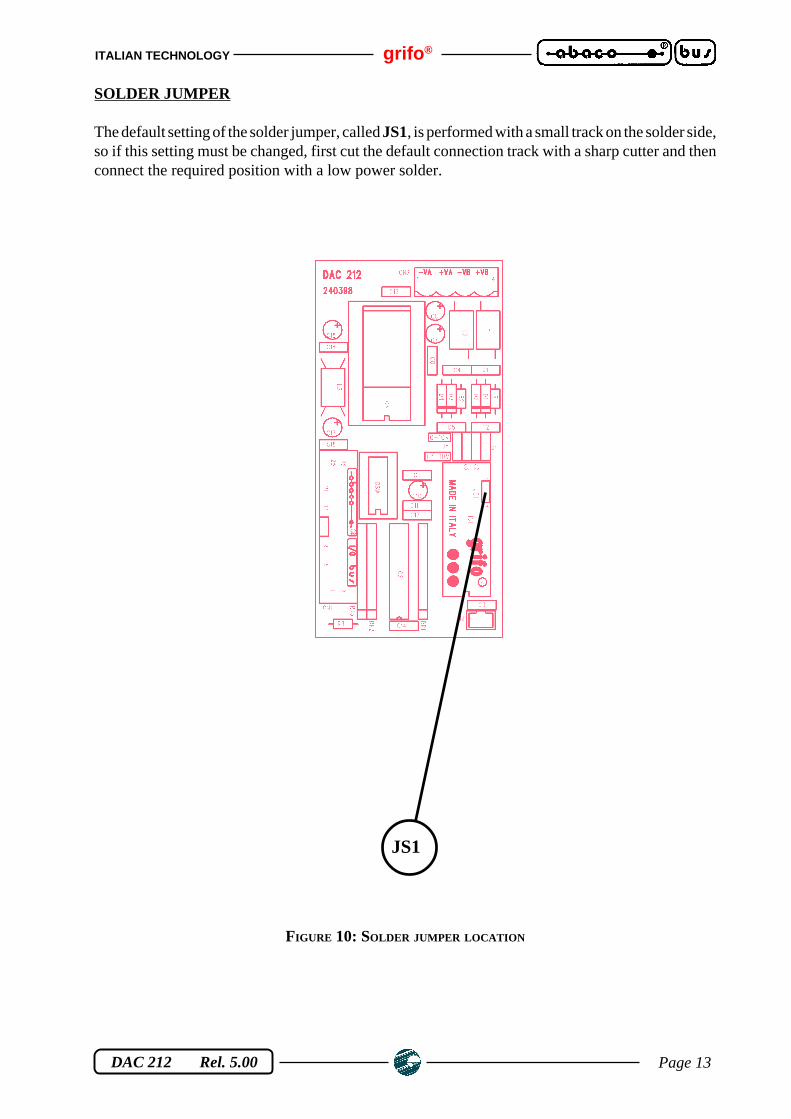
SOLDER JUMPER
The default setting of the solder jumper, called JS1, is performed with a small track on the solder side,so if this setting must be changed, first cut the default connection track with a sharp cutter and thenconnect the required position with a low power solder.
FIGURE 10: SOLDER JUMPER LOCATION
JS1

grifo ® ITALIAN TECHNOLOGY
Page 14 DAC 212 Rel. 5.00
BOARD CONNNECTIONS
To prevent possible connecting problems between DAC 212 board and the external systems, the userhas to read carefully the information of the previous paragraphs and he must follow theseinstrunctions:
- The analog outputs can erogate a maximum current of ±5 mA; for this reason they must be connected only to external circuits featuring a high impedance, which warrants not to exceed such current limit across the whole output range. Eventual connections to power actuators, like power motors, must be made through the specific power driver circuits, like, for exemple, activation or inverter.
- The TTL output signals can be connected directly only to a device featuring the same type of interface. About the correspondance between logic signals and TTL output status, remember that a logic 0 generates a TTL 0 Vdc, while a logic 1 generates a TTL +5 Vdc.
- If an external reference voltage is used, such voltage must be generated by a source noise-free, perfectly stable and indipendent from power supply and temperature. To fulfil every one of the above described requirements is essential for the correct working of the whole board. For further information please refer to paragraph “ELECTRIC FEATURES”.
REFERENCE VOLTAGE SELECTION
The solder jumper JS1, as previously described, allows to select the source for the Digital to Analogconverter DAC 2815 reference voltage.Such voltage can be the one generated on the DAC 212 board itself (JS1 in position 1-2), that provides+10 Vdc, or can be fetched from an external source through connector CN2 (JS1 in position 2-3).Such configuration, matched with J1÷J4 jumpers configuration, selects the range of the maximumoutput voltage for both the D/A channels, in detail:
JS1 in position 1-2 (internal Vref +10 Vdc)
J1÷J4 in position 1-2 -> Vout A, Vout B = ±10VJ1÷J4 in position 2-3 -> Vout A, Vout B = 0÷10V
JS1 in position 2-3 (external Vref )
J1÷J4 in position 1-2 -> Vout A, Vout B = ±VrefJ1÷J4 in position 2-3 -> Vout A, Vout B = 0÷Vref
RESET
When a Reset occours the analog outputs is set to 0 V, while in the write registers is put the value0 (000
HEX). For this reason if the DAC is configured for ±10 Vdc (or ±VRef) a read operation from
DACSET will set the outputs to value -10 Vdc (or -VRef), corresponding to the combination 0.To prevent this fact the user should initialize the write registers to the value 2048 (800
HEX), which
corresponds to the output voltage 0 Vdc.

ITALIAN TECHNOLOGY grifo ®
Page 15 DAC 212 Rel. 5.00
FIGURE 11: COMPONENTS MAP ON COMPONENT SIDE
FIGURE 12: COMPONENTS MAP ON SOLDER SIDE

grifo ® ITALIAN TECHNOLOGY
Page 16 DAC 212 Rel. 5.00
HARDWARE DESCRIPTIONHARDWARE DESCRIPTION
This chapter provides all the hardware informations needed to use DAC 212 board. Here the Userwill find informations about I/O card mapping and on board peripheral devices addressing.
BOARD MAPPING
DAC 212 board is mapped into a 4 bytes I/O addressing space that can be mapped starting fromdifferent base addresses according to how the board is configured. This feature allows to use severalDAC 212 cards on the same ABACO® I/O BUS or ABACO® BUS, or to install them on a BUS whereother peripheral modules are installed obtaining a structure that can be expanded without anydifficulty or modifications to the application software.These 4 bytes are accessible both in input and in output, so they allow a complete management ofthe board.The base address can be defined through the specific BUS interface circuitry on the board itself; thiscircuitry uses the six pins dip switch called DSW1, from which it reads the address set by the user.Here follows the corrispondance between dips configuration and address signals, to easily locate thedip switch please refer to figure 5.
DSW1.1 -> Address A2DSW1.2 -> Address A3DSW1.3 -> Address A4DSW1.4 -> Address A5DSW1.5 -> Address A6DSW1.6 -> Address A7
These dips are driven in complemented logic, this means that if a switch is ON generates a logiczero, viceversa if a switch is OFF generates a logic one.As an example, here is reported the configuration of DSW1 that allows to map the board resourcesfrom address 48H:
DSW1.1 -> ONDSW1.2 -> OFFDSW1.3 -> ONDSW1.4 -> ONDSW1.5 -> OFFDSW1.6 -> ON

ITALIAN TECHNOLOGY grifo ®
Page 17 DAC 212 Rel. 5.00
INTERNAL REGISTERS ADDRESSING
Indicating the board base address with <baseaddr>, that is the address set using DSW1, as indicatedin the previous paragraph, DAC 212 internal registers are addressable as explained in the followingtable.
FIGURE 13: INTERNAL REGISTERS ADDRESSING TABLE
NOTEIf using several boards on the same ABACO® I/O BUS, when setting the boards mapping addressthe user shold be careful not to allocate more than one board in the same addressing space (considerthe base address plus the bytes taken by the board addressing). If this condition is not satisfied a BUSconflict situation will occour, prejudicing the correct working of the whole system.Please remark that previous table reports the description of the registers available on DAC 212 card;for a detailed description of all the DAC 2815 Digital to Analog converter internal registers pleaserefer to next chapter.
DEVICE REG. ADDRESS R/W MEANING
DAC 2815
DACAL <baseaddr>+00H WWrites low byte into channel A controlregister.
DACAH <baseaddr>+01H WWrites high nibble into channel A controlregister.
DACBL <baseaddr>+02H WWrites low byte into channel B controlregister.
DACBH <baseaddr>+03H WWrites high nibble into channel B controlregister.
DACSET<baseaddr>+00H
....<baseaddr>+03H
RBoth channels A and B are set to the voltagevalue indicated by the data previouslywritten into the 4 control registers.

grifo ® ITALIAN TECHNOLOGY
Page 18 DAC 212 Rel. 5.00
PERIPHERAL DEVICES SOFTWARE DESCRIPTIONPERIPHERAL DEVICES SOFTWARE DESCRIPTION
In the previous paragraph allocation addresses of all the peripherals have been reported, here followsa detailed description of function and meaning of internal registers (please always refer to theperipheral mapping tables to understand completely the following informations). Should the presentdocumentaion be inadequate please refer to the component's manufacturer documentation.In the following paragraphs the indications D0÷D7 or D0÷D15 are used to refer the bits of the byteor word involved in the I/O operations.
D/A CONVERTER DAC 2815
Management of 12 bits D/A convertesr DAC 2815 is performed through read or write operations toits specific control registers described in figure 13.The meaning of the bits in the write registers is:
DACAL.D7 -> bit D7 of channel A DACBL.D7 -> bit D7 of channel BDACAL.D6 -> bit D6 of channel A DACBL.D6 -> bit D6 of channel BDACAL.D5 -> bit D5 of channel A DACBL.D5 -> bit D5 of channel BDACAL.D4 -> bit D4 of channel A DACBL.D4 -> bit D4 of channel BDACAL.D3 -> bit D3 of channel A DACBL.D3 -> bit D3 of channel BDACAL.D2 -> bit D2 of channel A DACBL.D2 -> bit D2 of channel BDACAL.D1 -> bit D1 of channel A DACBL.D1 -> bit D1 of channel BDACAL.D0 -> bit D0 of channel A DACBL.D0 -> bit D0 of channel B
DACAH.D3 -> bit D11 of channel A DACBH.D3 -> bit D11 of channel BDACAH.D2 -> bit D10 of channel A DACBH.D2 -> bit D10 of channel BDACAH.D1 -> bit D9 of channel A DACBH.D1 -> bit D9 of channel BDACAH.D0 -> bit D8 of channel A DACBH.D0 -> bit D8 of channel B
The meaning of the read register is:
DACSET -> Allows to set the output voltage of channels A and B with the twelvebits values previously set in the four write registers.
The instructions sequence to set an output voltage on a specific channel is:
- Write to opportune register the low byte (bits D7÷D0) of the 12 bits value.
- Write to the bits D0÷D3 of opportune register the high nibble (bits D11÷D8) of the 12 bits value.
- Perform a read operation from the register DACSET to set the output voltage of channels A and B with the twelve bits values previously set in the write register.

ITALIAN TECHNOLOGY grifo ®
Page 19 DAC 212 Rel. 5.00
The 12 bit data that is written into registers is proportional to the output voltage,according to therelation:
FIGURE 14: CORRESPONDANCE BETWEEN DIGITAL VALUE AND ANALOG OUTPUT VALUE
If , for example, the user wants to set the analog output value +6.25 Vdc in channel B of DAC2815,configured for output range 0÷10 Vdc, then he/she must perform the following operations:
- The 12 bit digital value to write into D/A registers is: 2560 (A00HEX
).- Write data 10 (0A
HEX) into register DACBH.
- Write data 0 (00HEX
) into register DACBL.- Read DACSET register to set the voltage output value.
If , for example, the user wants to set the analog output value -1.25 Vdc in channel A of DAC2815,configured for output range ±10 Vdc, then he/she must perform the following operations:
- The 12 bit digital value to write into D/A registers is: 1792 (700HEX
).- Write data 0 (00
HEX) into register DACAL.
- Write data 7 (07HEX
) into register DACAH.- Read DACSET register to set the voltage output value.
NOTEWhen a Reset occours (signal on pins 20 of CN1) the outputs of the two channels are set to 0 V, whilein the four write registers is put the value 0 (000
HEX).
For this reason if the DAC is configured for ±10 Vdc (or ±VRef) a read operation from registerDACSET without having opportunely initialized the write registers will cause the output voltagesto set to the value -10 Vdc (or -VRef), corresponding to the combination 0.To prevent this fact the user should initialize the write registers to the value 2048 (800
HEX), which
corresponds to the output voltage 0 Vdc.No one of these operations is required if the DAC is configured for 0÷10 Vdc (or 0÷VRef), in suchcase a combination 0 already corresponds to 0 Vdc as output voltage.
DIGITAL VALUE(Bit D11÷D0)
ANALOG OUTPUTS CONFIGURATION
0÷VRef Vdc 0÷10 Vdc ±VRef Vdc ±10 Vdc
4095 = FFFHEX +VRef Vdc +10 Vdc +VRef Vdc +10 Vdc
2047 = 7FFHEX +VRef / 2 Vdc +5 Vdc 0 Vdc 0 Vdc
0 0 Vdc 0 Vdc -VRef Vdc -10 Vdc

grifo ® ITALIAN TECHNOLOGY
Page 20 DAC 212 Rel. 5.00
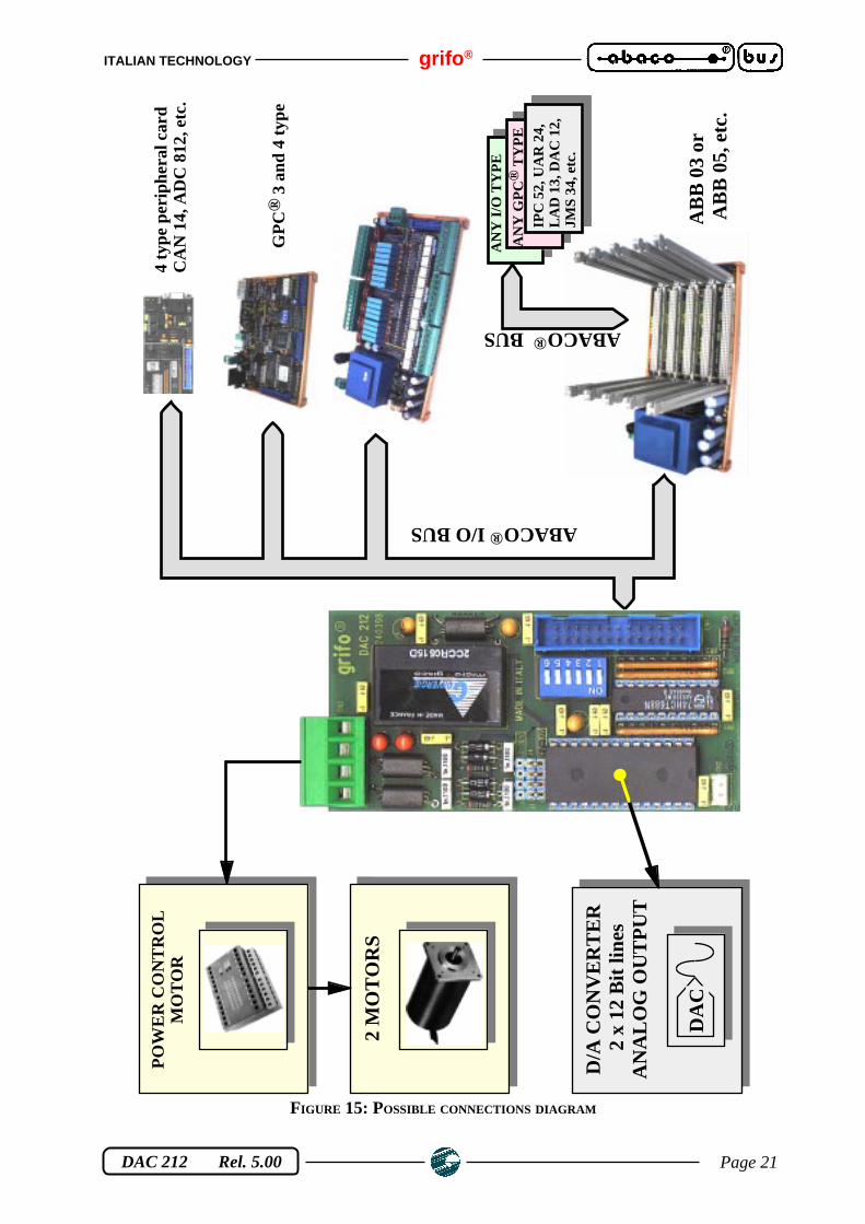
EXTERNAL CARDSEXTERNAL CARDS
DAC 212 can be connected to a wide range of block modules and operator interface system producedby grifo ®, or to many system of other companies.The on board resources can be expanded with asimple connection to the numerous peripheral grifo ® boards,both intelligent and not, thanks to itsstandard ABACO® I/O BUS connector. Even cards with ABACO® BUS can be connected, by usingthe proper mother boards.Hereunder some of these cards are briefly described; ask the detailed information directly to grifo ®,if required.
MB3 01-MB4 01-MB8 01Mother Board 3, 4, 8 slots
Motherboard featuring 3, 4 or 8 slots of ABACO® industrial BUS; pitch 4 TE; standard power supplyconnectors; LEDs for visual feed-back of power supply; holes for rack docking.
SPB 04-SPB 08Switch Power BUS 4-8 slots
Motherboard featuring 4-8 slots of ABACO ® industrial BUS; pitch 4 TE; standard power supplyconnectors; termination resistances; connector type F for SPC xxx supply ; holes for rack docking.
ABB 03ABACO® Block BUS 3 slots
3 slots ABACO® mother board; 4 TE pitch connectors; ABACO® I/O BUS connector; screwterminal for power supply; connection for DIN C type and Ω rails.
ABB 05ABACO® Block BUS 5 slots
5 slots ABACO® mother board with power supply. Double power supply built in; 5Vdc 2,5A sectionfor powering the on board logic; second section at 24Vdc 400mA galvanically coupled, for theoptocoupled input lines. Auxiliary connector for ABACO® I/O BUS. Connection for DIN Ω rails.
SBP 02-xxSwitch BLOCK Power xx version
Low cost switching power supply able to generate voltage from +5 to +40 Vdc and current up to 2.5A; Input from 12 to 24 Vac; Connection for DIN C Type and Ω rails.
SPC 03.5SSwitch Power Card +5 Vdc
Europe format switching power supply capable to provide +5 Vdc to a load of 4 A; input voltage12÷24 Vac; power-failure; connector for back-up battery; standard connector for mother board SPB0x.
SPC 512Switch Power Card +5 Vdc +12 Vdc
Europe format switching power supply capable to provide +5 Vdc 5A and +12 Vdc 2.5 A; inputvoltage 12÷24 Vac; power-failure; connector for back-up battery; standard connector for motherboard SPB 0x.
ITALIAN TECHNOLOGY grifo ®
Page 21 DAC 212 Rel. 5.00
FIGURE 15: POSSIBLE CONNECTIONS DIAGRAM
ABACO® I/O BUS A
BB
03
or
AB
B 0
5, e
tc.
AN
Y G
PC
® T
YP
E
IPC
52,
UA
R 2
4,
LAD
13,
DA
C 1
2,
JMS
34,
etc
.
AN
Y I/
O T
YP
E
ABACO® BUS
GP
C®
3 a
nd 4
type
4 ty
pe p
erip
hera
l car
d C
AN
14,
AD
C 8
12, e
tc.
2 M
OT
OR
S
PO
WE
R C
ON
TR
OL
MO
TO
R
DA
C
D/A
CO
NV
ER
TE
R 2
x 1
2 B
it lin
esA
NA
LOG
OU
TP
UT

grifo ® ITALIAN TECHNOLOGY
Page 22 DAC 212 Rel. 5.00
GPC® 153General Purpose Controller Z80
84C15 µP, 10÷16 MHz; Full CMOS; 1 RS 232 line; 1 RS 232 or RS 422-485 or Current Loop line;16 TTL I/O lines; 8 A/D 12 bits lines; 2÷4 Timers Counters; 512K EPROM or FLASH; 512K RAMand RTC backed; 8K serial EEPROM; Buzzer; 1 Activity LED; Watch dog; 8 readable DIPs; LCDInterface.
GPC® 183General Purpose Controller Z180
Z180 µP, 10÷16 MHz; Full CMOS; 1 RS 232 line; 1 RS 232 or RS 422-485 or Current Loop line;24 TTL I/O lines; 11 A/D 12 bits lines; 2 Timers Counters; 512K EPROM or FLASH; 512K RAMand RTC backed; 8K serial EEPROM; Buzzer; 2 Activity LED; Watch dog; 4 readable DIPs; LCDInterface.
GPC® 324/D“4” Type General Purpose Controller 80C32/320
80C32 or 80C320 µP, 14÷22 MHz; Full CMOS; 1 RS 232 line; 1 RS 232 or RS 422-485 or CurrentLoop line; 4÷16 TTL I/O lines; 3 Timers Counters; 64K EPROM; 64K RAM; 32K RAM backed;32K DIL E2; 8K serial EEPROM; Watch dog; 1 readable DIP; LCD Interface; Abaco® I/O BUS;5Vdc Power supply; Size: 100x50 mm.
GPC® 554General Purpose Controller 80C552
Microprocessor 80C552 at 22 MHz; implementation completely CMOS; 32K EPROM; 32 KSRAM; 32 K EEPROM or SRAM; EEPROM; 2 RS 232 serial lines; 16 I/O TTL; 2 PWM lines; 16bits Timer/Counter; Watch Dog; 6 signals A/D converter with resolution 10 bit; interface forABACO® I/O BUS.
GPC® 154“4” Type General Purpose Controller Z80
84C15 µP, 10÷16 MHz; Full CMOS; 1 RS 232 line; 1 RS 232 or RS 422-485 line; 16 TTL I/O lines;2÷4 Timers Counters; 512K EPROM or FLASH; 512K RAM and RTC backed; 8K serial EEPROM;Watch dog; 2 readable DIPs; LCD Interface; Abaco® I/O BUS; 5Vdc Power supply; Size: 100x50mm.
GPC® 884General Purpose Controller Am188ES
Microprocessor AMD Am188ES up to 40 MHz16 bits; implementation completely CMOS; serie 4format; 512K EPROM or FLASH; 512K SRAM backed with Lithium battery; RTC; 1 RS 232 serialline + 1 RS 232 or RS 422-485 or current loop; 16 I/O TTL; 3 timer/counter; watch dog; EEPROM;11 signals A/D converter with 12 bit resolution; interface for ABACO® I/O BUS.
GPC® 114General Purpose Controller 68HC11
Microprocessor 68HC11A1 at 8 MHz; implementation completely CMOS; serie 4 format; 32KEPROM; 32K SRAM backed with Lithium battery; 32K EPROM, SRAM, EEPROM; RTC; 1 serialline RS 232 or RS 422-485; 10 I/O TTL; 3 timer/counter; watch dog; 8 signals A/D converter withresolution 8 bit; 1 asunchronous serial line; extremly low power consumption; interface forABACO® I/O BUS.

ITALIAN TECHNOLOGY grifo ®
Page 23 DAC 212 Rel. 5.00
PBI 01PNP BLOCK Input
Interface for PNP drivers through NPN inputs; 16 inputs for driver PNP, visualized by LEDs; 16NPN outputs on ABACO® standard input connector; Plastic mount for rails DIN 46277-1 and 3.
FBC 20-120Flat Block Contact 20 vie
Interface for 2 or 1 mounting cable connectors (low profile 20 pins male) and quick release screwterminal connectors; Plastic mount for rails DIN 46277-1 and 3.
FBC 34Flat Block Contact 34 vie
Interface for 2 mounting cable connector (low profile 34 pins male) and quick release screw terminalconnectors; Plastic mount for rails DIN 46277-1 and 3.
FBC L20Flat Block Contact LED 20 vie
Interface for 1 mounting cable connector (low profile 20 pins male,featuring ABACO® standardInput pin out, and quick release screw terminal connectors; All the signals are visualized throughLEDs; Plastic mount for rails DIN 46277-1 and 3.
FBC L34Flat Block Contact LED 34 vie
Interface for 2 mounting cable connectors (low profile34 and 20 pins male) and quick release screwterminal connectors; featuring ABACO ® standard Input and Output pin out; All the signals arevisualized through LEDs; Plastic mount for rails DIN 46277-1 and 3.

grifo ® ITALIAN TECHNOLOGY
Page 24 DAC 212 Rel. 5.00
BIBLIOGRAPHYBIBLIOGRAPHY
Here follows a list of manuals and technical notes that the User can read to acquire more informationsabout DAC 212 board.
Manual BURR-BROWN: Integrated circuits data book supplementent - Volume 33c
Manual TEXAS-INSTRUMENTS: The TTL Data Book - SN54/74 Families
Technical Note MICRO-GISCO: DC-DC Converter 2CCR0515D
Please connect to the manifactures Web sites to get the latest version of all manuals and data sheets.

ITALIAN TECHNOLOGY grifo ®
Page A-1 DAC 212 Rel. 5.00
APPENDIX A: ALPHABETICAL INDEXAPPENDIX A: ALPHABETICAL INDEX
SYMBOLS
+VREF 10±15 VDC 4
A
ABACO ® BUS 16, 20ABACO ® I/O BUS 4, 5, 8, 16, 17, 20ADDRESSING 4ADDRESSING SPACE 16ANALOG OUTPUTS 6, 14
B
BIBLIOGRAPHY 24BOARD CONNNECTIONS 14BOARD MAPPING 16
C
CARD VERSION 1CONNECTIONS 6
CN1 8CN2 10CN3 6
CONNECTORS 5CURRENT CONSUMPTION 5
D
D/A CONVERTER 4, 18D/A MAXIMUM OUTPUT CURRENT 5D/A REFERENCE VOLTAGE 5D/A VOLTAGE OUTPUTS RANGE 5DAC 2815 4, 14, 17, 18DACAH 18DACAL 18DACBH 18DACBL 18DACSET 18DC/DC CONVERTER 4DSW1 4, 16, 17

grifo ® ITALIAN TECHNOLOGY
Page A-2 DAC 212 Rel. 5.00
E
ELECTRIC FEATURES 5EXTERNAL CARDS 20EXTERNAL REFERENCE VOLTAGE 10, 14
G
GENERAL FEATURES 5GENERAL INFORMATION 2
H
HARDWARE DESCRIPTION 16
I
INSTALLATION 6INTERFACING 4INTERNAL REGISTERS ADDRESSING 17INTRODUCTION 1
J
JS1 13, 14JUMPERS 11
3 PINS JUMPERS 12
M
MECHANICAL MOUNTING 11
P
PERIPHERAL DEVICES SOFTWARE DESCRIPTION18PHYSICAL FEATURES 5POWER SUPPLY 5
R
REFERENCE VOLTAGE SELECTION 14RELATIVE HUMIDITY 5RESET 14, 19
S
SIZE 5SOLDER JUMPER 13
ITALIAN TECHNOLOGY grifo ®
Page A-3 DAC 212 Rel. 5.00
T
TECHNICAL FEATURES 5TEMPERATURE RANGE 5TTL 14
V
VREF 4VREF MAXIMUM RANGE 5
W
WEIGHT 5

grifo ® ITALIAN TECHNOLOGY
Page A-4 DAC 212 Rel. 5.00