d037/d038/d040/d041 point to point diagram (1/2) · ictl pcb2 psu 1/2 pcb1 bcu (1/2) pcb3 dr cn911...
TRANSCRIPT

iCTLPCB2
PSU 1/2PCB1
BCU (1/2) PCB3
DR
CN
502
CN
911
CN213CN215
CN251 CN250
CN208
-1 -2 -3 -4
Deb
ug M
onito
r: R
XD
(PC
->B
CU
)D
ebug
Mon
itor:
+5V
Deb
ug M
onito
r: G
ND
Deb
ug M
onito
r: TX
D(B
CU
->P
C)
CN
912
-1-2-3-4
-1-2-3-4
-1-2-3-4
-1-2-3-4
CN
503
+5V
GNDGND
+5VE
+5VLDGNDGND+24V
-4 -3 -2 -1-8 -7 -6 -5-12
-11
-10 -9-13
-14
-18
-17
-16
-15
-19
-20
-24
-23
-22
-21
-28
-27
-26
-25
-30
-29
-34
-33
-32
-31
-36
-35
-37
-38
Res
erve
Fan
: HR
eser
ve F
an: L
Res
erve
Fan
: LO
CK
det
ect
GN
D
BAN
K: P
aper
Fee
d C
L 2
BAN
K: P
aper
Fee
d C
L 1
BAN
K: S
elec
ter B
BAN
K: S
elec
ter A
BAN
K: C
onne
ctio
nB
ANK:
Pap
er H
eigh
tB
ANK:
Pap
er S
ize
Switc
h: T
2B
ANK:
Pap
er S
ize
Switc
h: T
1
BAN
K: R
elay
Clu
tch
BAN
K: R
elay
Sen
sor
BAN
K: L
ift 2
BAN
K: L
ift 1
BAN
K: P
aper
End
Sen
sor:
T2B
ANK:
Pap
er E
nd S
enso
r: T1
+24V
S3
-1 -2 -3 -4 -5 -6 -7 -8 -9 -10
-11
-12
-13
-14
-15
-16
-17
-18
-19
-20
-22
-23
-24
-25
-26
-27
-28
-29
-31
-32
-33
-34
-35
-21
-30
-36
-37
-38
-4 -3 -2 -1-8 -7 -6 -5-12
-11
-10 -9-13
-14
-18
-17
-16
-15
-19
-20
-1 -2 -3 -4 -5 -6 -7 -8 -9 -10
-11
-12
-13
-14
-15
-16
-17
-18
-19
-20
-40
-24
-23
-22
-21
-28
-27
-26
-25
-30
-29
-34
-33
-32
-31
-36
-35
-37
-38
-39
-40
-22
-23
-24
-25
-26
-27
-28
-29
-31
-32
-33
-34
-35
-21
-30
-36
-37
-38
-39
ID S
enso
r/ITB
Con
tact
Mot
or:O
ver-C
urre
nt D
etec
t
PTR
Con
tact
Mot
or: D
IAP
TR C
onta
ct M
otor
: DIB
PSU
Fan
N.C
.
BAN
K: L
ift M
T 1:
DIA
BAN
K: L
ift M
T 1:
DIB
BAN
K: L
ift M
T 2:
DIA
BAN
K: L
ift M
T 2:
DIB
BAN
K: T
rans
port
MT:
ON
BAN
K: H
igh/
Low
BAN
K: T
rans
port
MT:
LD
+5V
ITB
Con
tact
Mot
or: D
IAIT
B C
onta
ct M
otor
: DIB
GN
D+2
4VS
3
Fini
sher
: RX
D_I
Fini
sher
: TX
D_O
GN
D
PC
U T
oner
Col
lect
ion
Mot
or
Lens
Pos
ition
ing
Mot
or-M
: /A
Ser
ies:
C
ON
TRO
L
Lens
Pos
ition
ing
Mot
or-M
: /B
Ser
ies:
C
ON
TRO
L
Lens
Pos
ition
ing
Mot
or-M
: B S
erie
s: C
ON
TRO
LLe
ns P
ositi
onin
g M
otor
-M:A
Ser
ies:
CO
NTR
OL
Lens
Pos
ition
ing
Mot
or-Y
: /A
Ser
ies:
CO
NTR
OL
Lens
Pos
ition
ing
Mot
or-Y
: /B
Ser
ies:
CO
NTR
OL
Lens
Pos
ition
ing
Mot
or-Y
:B S
erie
s: C
ON
TRO
LLe
ns P
ositi
onin
g M
otor
-Y: A
Ser
ies:
CO
NTR
OL
Lens
Pos
ition
ing
Mot
or-C
: /A
Ser
ies:
CO
NTR
OL
Lens
Pos
ition
ing
Mot
or-C
: /B
Ser
ies:
CO
NTR
OL
Lens
Pos
ition
ing
Mot
or-C
: B S
erie
s: C
ON
TRO
LLe
ns P
ositi
onin
g M
otor
-C:A
Ser
ies:
CO
NTR
OL
Lase
r Uni
t Fan
: LO
CK
Det
ect
Lase
r Uni
t Fan
: LLa
ser U
nit F
an: H
PC
U T
oner
Col
lect
ion
Mot
or: S
et D
etec
t
Fusi
ng F
ront
Fan
: LO
CK
Det
ect
Fusi
ng F
ront
Fan
: LFu
sing
Fro
nt F
an: H
Fusi
ng R
ear F
an: L
OC
K D
etec
tFu
sing
Rea
r Fan
: LFu
sing
Rea
r Fan
: H
Ven
tilat
ion
Fan:
Rea
r: LO
CK
Det
ect
Ven
tilat
ion
Fan:
Rea
r: L
Ven
tilat
ion
Fan:
Rea
r: H
Ven
tilat
ion
Fan:
Fro
nt: L
OC
K D
etec
tV
entil
atio
n Fa
n: F
ront
: LV
entil
atio
n Fa
n: F
ront
: H
Tone
r Sup
ply
Mot
or: K
Tone
r Sup
ply
Mot
or: C
Tone
r Sup
ply
Mot
or: M
Tone
r Sup
ply
Mot
or: Y
Reg
istra
tion
Mot
or: A
Ser
ies
Reg
istra
tion
Mot
or: A
Ser
ies
Reg
istra
tion
Mot
or: B
Ser
ies
Reg
istra
tion
Mot
or: /
B S
erie
s
Reg
istra
tion
Mot
or: C
urre
nt S
witc
hing
1
Reg
istra
tion
Mot
or: C
urre
nt S
witc
hing
2
CN553
SD CARD I/F
CN554
*
RGB FM I/F
CN511
RGB FM
USB I/F
CN55510/100
NETWORK I/F
CN556Serial Terminal
2ch
CN560
CN853
Registration Motor
M8
CN253
Reg
istra
tion
Mot
or: A
Ser
ies
Reg
istra
tion
Mot
or: /
A Se
ries
-1 -2 -3 -4 -5
Reg
istra
tion
Mot
or: B
Ser
ies
Reg
istra
tion
Mot
or: +
24VS
3R
egis
tratio
n M
otor
: /B
Serie
s-1-2-3-4-5-6
M6
CN256
-9 -10
M5
-7 -8
M4
-5 -6
M3
-3 -4
Tone
r Sup
ply
Mot
or: Y
: CO
NTR
OL
Tone
r Sup
ply
Mot
or: Y
: GN
D
Tone
r Sup
ply
Mot
or: C
: CO
NTR
OL
Tone
r Sup
ply
Mot
or: C
: GN
D
Tone
r Sup
ply
Mot
or: M
: CO
NTR
OL
Tone
r Sup
ply
Mot
or: M
: GN
D
Tone
r Sup
ply
Mot
or: K
: C
ON
TRO
LTo
ner S
uppl
y M
otor
: K: G
ND
M2
-1 -2IT
B C
onta
ct M
otor
: DIA
ITB
Con
tact
Mot
or: D
IB
CN1JCNCN
CN2JCNCN
CN3JCNCN
CN4JCNCN
CN5
-2 -1 -2 -1 -2 -1 -2 -1 -2 -1
1 2 1 2 1 2 1 2 1 2To
ner S
uppl
y M
otor
:Y
Tone
r Sup
ply
Mot
or:M
Tone
r Sup
ply
Mot
or:M
Tone
r Sup
ply
Mot
or:M
ITB
Con
tact
Mot
or
CN856JCN856CN856
-1 -2 -3 -4 -5 -6 -7 -8 -9 -10
-1-2-3-4-5-6-7-8-9-10
JCN5CN
M9
PTR
Con
tact
Mot
or1 2
CN254
Fusi
ng R
ear F
an: C
ON
TRO
LFu
sing
Rea
r Fan
: LO
CK
Det
ect
Fusi
ng R
ear F
an: +
24V5
-1
Fusi
ng F
ront
Fan
: CO
NTR
OL
Fusi
ng F
ront
Fan
: LO
CK
Det
ect
Fusi
ng F
ront
Fan
: +24
V5
-2 -3 -4 -5 -6
-2 -1Fu
sing
Rea
r Fan
CN844JCN
1 2
F6
CN
-2 -1Fu
sing
Fro
nt F
an
CN845JCN845
1 2
F7
CN
3 3
-3 -3
CN846
JCN846
CN
-1-2-7 -8
PTR
Con
tact
Mot
or: D
IAPT
R C
onta
ct M
otor
: DIB
CN854JCN854CN854
-7-8-1 -2
-1-2-3-6 -7 -8
-4-5-6-3 -4 -5
-2 -1La
ser U
nit F
an
CN3JCN3
CN260
Lase
r Uni
t Fan
: CO
NTR
OL
Lase
r Uni
t Fan
: LO
CK
Det
ect
Lase
r Uni
t Fan
: +24
V5
CN860JCN860
-2 -1
-1 -2
CN860
-3
-3-3
-1 -2 -3
1 2
CN
3
F3
CN
224
CN
910
-1-2-3-4-5-6-7-8-9 -1
-2-3-4-5-6-7-8-9
PSU: Heating Lamp Triger: Ends
PSU: +24VSRPSU: GNDPSU: Relay TrigerPSU: Heating Lamp Triger: CenterPSU: Pressure Lamp Triger
PSU: Zero Cross SignalPSU: PONENG_NPSU: +5VE
CN
225
CN
913
CN
252
-1-2-3-4
-2-1
-3-4
PSU: GND
PSU: +24V6PSU: GND
PSU: +24V5
PSU: +5VPSU: GNDPSU: GNDPSU: GNDPSU: GND
PSU: +24V2PSU: +24V3PSU: +24V4
-1-2-3-4-5-6-7-8
-11-12
-5-6-7-8-9-10
-1-2C
N91
5
RELAY(-)RELAY(+) C
N89
0-1-2
-3-4-5 -1
-2-3 C
N26
2
PSUFAN1PSUFAN2
+24V5FAN
JCN
890
CN
903
-1
-3
-2
-4AC-N-ON
AC-N
Main Switch
AC-L-ON
AC-LT1
T4
T2
T3
PSU Fan 1 FAN1-1-2
FCN
1
-3
24V5FAN
PSUFAN1N.C.
PSU Fan 2 FAN
-1-2
FCN
2
-3
24V5FAN
PSUFAN2N.C.
CN
500
iCTL
I/F
CN
210
Laser Unit
CN259
Lens Positioning
Motor-Y
CN9
M10
Lens Positioning
Motor-M
CN10
M11
Lens Positioning Motor-C
CN11
M12
Lens
Pos
ition
ing
Mot
or-C
: +24
V5
Lens
Pos
ition
ing
Mot
or-C
: /A
Ser
ies
Lens
Pos
ition
ing
Mot
or-C
: /B
Ser
ies
Lens
Pos
ition
ing
Mot
or-C
: B S
erie
sLe
ns P
ositi
onin
g M
otor
-C: A
Ser
ies
Lens
Pos
ition
ing
Mot
or-M
: +24
V5
Lens
Pos
ition
ing
Mot
or-M
/A S
erie
sLe
ns P
ositi
onin
g M
otor
-M: /
B S
erie
s
Lens
Pos
ition
ing
Mot
or-M
: B S
erie
sLe
ns P
ositi
onin
g M
otor
-M: A
Ser
ies
Lens
Pos
ition
ing
Mot
or-Y
: +24
V5
Lens
Pos
ition
ing
Mot
or-Y
: /A
Serie
sLe
ns P
ositi
onin
g M
otor
-Y: /
B Se
ries
Lens
Pos
ition
ing
Mot
or-Y
: B S
erie
sLe
ns P
ositi
onin
g M
otor
-Y: A
Ser
ies
CN859CN859
CN3
-1-2-3-4-5-1-2-3-4-5-1-2-3-4-5-1 -2 -3 -4 -5 -6 -7 -8 -9 -10
-11
-12
-13
-14
-15
-1 -2 -3 -4 -5 -6 -7 -8 -9 -10
-11
-12
-13
-14
-15
-1-2-3-4-5-6-7-8-9-10
-11
-12
-13
-14
-15
CN
8C
N7
Polygon Mirror Motor
CN
6
CN
2JC
N87
0C
N87
0
CN
510
-1-2-3-4-5-6-7-8-9
-10-11-1
-2-3-4-5-6-7-8-9-10-11
-1-2-3-4-5
-1-2-3-1-2-3
-1-2-3-4-5-6-7-8-9
-10-11K
Y
M13
LDB:ST12PCB13
LDB:ST34PCB14
CN
4C
N5
JCN
1C
N1
CN
1
CN
509
CN
508
-1
-16
~
-1
-16
~
-1
-16
~
-17
-32
~
-17
-1
-16
~
-17
-32
~
-1
-16
~
-17
~
-1-2
CN255
CN855JCN855CN855
-1 -2-7-8
Tone
r Col
lect
ion
Mot
or: +
24V
S3To
ner C
olle
ctio
n M
otor
: CO
NTR
OL
CN3JCN3
-1 -2-1-2
Tone
r Col
lect
ion
Mot
or
-1 -2 -3-1-2-3
Vent
ilatio
n Fa
n: R
ear:
CO
NTR
OL
Vent
ilatio
n Fa
n: R
ear:
LOC
K D
etec
tVe
ntila
tion
Fan:
Rea
r: +2
4V5
-3 -2 -1
CN1JCN1
-6 -7 -8V
entil
atio
n Fa
n: R
ear
-3 -2 -1Ve
ntila
tion
Fan:
Fro
nt: C
ON
TRO
L
CN2JCN2
-3 -4 -5-4-5-6
-3 -4 -5Ve
ntila
tion
Fan:
Fro
nt: L
OC
K D
etec
tVe
ntila
tion
Fan:
Fro
nt: +
24V5
Ven
tilat
ion
Fan:
Fro
nt
1 2 3
F5
CN
1 2 3
F4
CN
M7
1 2
CN
CN264
-4N
.C.
T901
T902
AC_L (Black)
AC_N (White)
AC Cord*
CN
906
-1
-6
-2
-5
N.C.
AC-SW-IN
N.C.
AC-SW-OUT
CN
2
Tray Heater (Option)
-4
-3
-1
-2
AC-L-FEED
AC-N-FEED
CN
908
CN
1
-5
-1
-1
-2
AC-L-SCN
AC-N-SCN
-4
-2 AC-N-PCU
AC-L-PCU
-3N.C.
Anti-condensation Heater - Scanner (Option)
CN
907
CN
3
-3
-1-2
AC-L-BANK
AC-N-BANK
-1-2
N.C.
Optional Tray Heater (Option)
-1
L-IN
L-OUT
-2
Choke Coil
*200V series only
CN
L
CN504ICIB I/F
(Copy Data Security Unit Type F)
ICIB
USB2.0 Host I/F
CN551
Fusion
*D038/D041 only
USB2.0 Host I/FCN5 CN4
General-purpose SD CARD I/F
CN1
CN551 *C1H only
ExclusiveDIMM512MB
*D038/D041 only
DDR DIMM I/F
CN562
DIMM256MB
*D038/D041 only
CN565
DIMM512MB
HDDHDD1
CN564
CN1
CN563
CN
HD
D:G
ND
HD
D:5
VE
PH
DD
:GN
D-3 -2 -1
-1-2-3
-3 -2 -1-1-2-3
-4-5-6-7
-4-5-6-7
HD
D:G
ND
HD
D:T
XP
HD
D:T
XN
HD
D:R
XP
HD
D:R
XN
HD
D:G
ND
HD
D:G
ND
*D038/D041 only
Exclusive
MKB
CN752
-1 -2 -3 -4 -5 -6
-4 -3 -2 -1-6 -5
CN753
CN505
MK
B:5V
EM
KB:
5VE
MK
B:PE
TXD
MK
B:PE
RXD
MK
B:G
ND
MK
B:G
ND
-4 -3 -2 -1-7 -6 -5
Cha
rgin
g U
nit:G
ND
Cha
rgin
g U
nit:R
XDC
harg
ing
Uni
t:TX
DC
harg
ing
Uni
t:GN
DC
harg
ing
Uni
t:5V
EC
harg
ing
Uni
t:5V
EC
harg
ing
Uni
t:GN
D
Keycard(Serial)
CN
-1 -2 -3 -4 -5 -6 -7
MKB
CN216
CN750
-4 -3 -2 -1-8 -7 -6 -5-12
-11
-10 -9-13
-1 -2 -3 -4 -5 -6 -7 -8 -9 -10
-11
-12
-13
Key
Car
d: +
5VKe
y C
ard:
Set
Det
ect
Key
Car
d: M
KB
_b0
Key
Car
d: M
KB
_b1
Key
Car
d: M
KB
_b2
Key
Car
d: M
KB
_b3
Key
Car
d: M
KB
_b4
Key
Car
d: M
KB
_b5
Key
Car
d: M
KB
_b6
Key
Car
d: M
KB
_b7
Key
Car
d: G
ND
Key
Car
d: C
OU
NT
Key
Car
d: +
24V
CN
T
CN751
Keycard(Parallel)
CN
Cha
rgin
g U
nit:C
ON
TRO
L
Cha
rgin
g U
nit:D
ATA
7C
harg
ing
Uni
t:DA
TA8
Cha
rgin
g U
nit:2
4V_C
NT
Cha
rgin
g U
nit:S
et D
etec
t
Cha
rgin
g U
nit:5
VC
harg
ing
Uni
t:5V
Cha
rgin
g U
nit:5
VC
harg
ing
Uni
t:5V
Cha
rgin
g U
nit:5
VC
harg
ing
Uni
t:5V
Cha
rgin
g U
nit:5
VC
harg
ing
Uni
t:5V
Cha
rgin
g U
nit:D
ATA
5C
harg
ing
Uni
t:DA
TA6
Cha
rgin
g U
nit:D
ATA
3C
harg
ing
Uni
t:DA
TA4
Cha
rgin
g U
nit:D
ATA
1C
harg
ing
Uni
t:DA
TA2
Cha
rgin
g U
nit:G
ND
-B2
-B1
-B3
-B4
-B8
-B7
-B6
-B5
-B10 -B9
-A4
-A3
-A2
-A1
-A8
-A7
-A6
-A5-
A10 -A9
B1 B2 B3 B4 B5 B6 B7 B8 B9 B10 A1 A2 A3 A4 A5 A6 A7 A8 A9 A10
PCI Option I/F
Hand Set
CN557 B
CN600
GWFCU 3SD-RAM
DIMM:32MB(PC100)
BAT
12060084
CN601CN630
MBU12060082
BAT
FAX UNI(Standard for Model 765)
CN621
TEL(DOM)(EXP)
CN620
LINE1(DOM)(EXP)
CN
608
CN
605-2
-1SPSpeaker +24V
GND
CN557 A
* C1H only
Bluetooth
IEEE1284
IEEE802.11g
GigaEther
MLB32
* C1H only CN506
OP
U: G
ND
OP
U: O
P_T
CLK
OP
U: G
ND
OP
U: O
P_R
XDO
PU
: OP
_TXD
OP
U: P
W_S
W_N
OP
U: +
5VO
PU
: +5V
E
-4 -3 -2 -1-8 -7 -6 -5
-1 -2 -3 -4 -5 -6 -7 -8
OPUPCB4
CN730
CNCN
FAX OP
Operation Panel *D037 only
OPU
CN507
-4 -3 -2 -1-8 -7 -6 -5-12
-11
-10 -9
-1 -2 -3 -4 -5 -6 -7 -8 -9 -10
-11
-12
OPU
: OP_
RX
DO
PU: O
P_R
CLK
OPU
: GN
DO
PU: O
P_TC
LK
OPU
: PW
_SW
_NO
PU: +
5VE
OPU
: OP_
RE
Q_N
OPU
: GN
D
OPU
: OP_
TXD
OPU
: +5V
OPU
: +5V
OPU
: +24
V
CN700
LCDCPCB5
OP - LPCB6
OP - RPCB7
Inverter:TFFPCB8
Operation Panel
*D038/D041 only
SBU
: LV
DS
CLK
1-SB
U: L
VD
SC
LK1+
SBU
: LV
DS
CLK
2-SB
U: L
VD
SC
LK2+
Exp
osur
e La
mp
CN101
CN2
-3 -2 -1
CN3
-3 -2 -1
S3 S4
-1 -2 -3 -4 -5 -6
CN205
Scan
ner H
P Se
nsor
: GN
DS
cann
er H
P S
enso
r: O
UTP
UT
Sca
nner
HP
Sen
sor:
+5V
PCB9
Scanner Unit
S2
-1 -2 -3 -4 -5 -6 -7
CN1
-3 -2 -1
CN2
-3 -2 -1
S1
CN300
-B1
-B2
-B3
-B4
-B5
-B6
-B7
-B8
-B9
-B10
-B11
-B12
-B13
-B14
-B15 -A
1
-A2
-A3
-A4
-A5
-A6
-A7
-A8
-A9
-A10
-A11
-A12
-A13
-A14
-A15
CN501
CN202
CN301
-1 -2 -3 -4 -5 -6 -7 -8 -9 -10
-11
-12
-13
-14
-15
-16
-17
-1-2-3-4-5-6-7-8-9-10
-11
-12
-13
-14
-15
-16
-17
SBU
: +3.
3V_S
BU
SBU
: GN
DSB
U:L
AM
P O
N C
LK
SBU
: +10
V_SB
USB
U: +
5V
SBU
: GN
DS
BU: G
ND
SBU
: GN
DS
BU: G
ND
SBU
:+ 3
.3V_
SBU
SBU
:+ 3
.3V_
SBU
SBU
: GN
DS
BU: G
ND
SBU
:+ 5
.83V
_SB
US
BU: +
5.83
V_S
BU
SBU
: GN
DSB
U: +
5V
-1 -2 -3 -4 -5 -6
CN204
-1 -2 -3 -4 -5 -6
M1
Scan
ner M
otor
Sca
nner
Mot
or:/A
Ser
ies
Sca
nner
Mot
or:+
24V
4S
cann
er M
otor
:/B S
erie
sSc
anne
r Mot
or:A
Ser
ies
Sca
nner
Mot
or:+
24V
4Sc
anne
r Mot
or:B
Ser
ies
CN1CN1
CN203
-1 -2 -3 -4
-1 -2 -3 -4
Orig
inal
Len
gth
Sens
or 1
: GN
DO
rigin
al L
engt
h S
enso
r 1: O
UTP
UT
Orig
inal
Len
gth
Sen
sor 1
: +5V
APS
Orig
inal
Len
gth
Sens
or 2
: GN
DO
rigin
al L
engt
h S
enso
r 2: O
UTP
UT
Orig
inal
Len
gth
Sen
sor 2
:+5V
APS
-A1
-A2
-A3
-A4
-A5
-A6
-A7
-A8
-A9
-A10
-A11
-A12
-A13
-A14
-A15
-B1
-B2
-B3
-B4
-B5
-B6
-B7
-B8
-B9
-B10
-B11
-B12
-B13
-B14
-B15
CN206
N.C
.
SBU
:XC
NSB
USB
U: G
ND
SBU
: GN
DSB
U: G
ND
SBU
: TC
1-
SBU
: TB
1-
SBU
: GN
DSB
U: G
ND
SBU
: TC
1+
SBU
: TB
1+
SBU
: TC
2-SB
U: T
C2+
SBU
: TB
2-SB
U: T
B2+
SBU
: TA
2-SB
U: T
A2+
SBU
: SY
CLK
SBU
: XS
YCS
SBU
: SY
DO
SBU
: SY
DI
SBU
: GN
DSB
U: X
SLE
ADSB
U: X
SFG
ATE
SBU
: XS
LSYN
CSB
U: G
ND
SBU
: GN
D
NCLV HV
NC
-3 -2 -1-4
Orig
inal
Len
gth
Sens
or 1
Orig
inal
Len
gth
Sen
sor 2
Pla
ten
Cov
er
Sen
sor
Sca
nner
HP
S
enso
rPl
aten
Cov
er S
enso
r: G
ND
Pla
ten
Cov
er S
enso
r: O
UTP
UT
Pla
ten
Cov
erSe
nsor
: +5V
ESN
S
Lam
p St
abiliz
er:L
AM
P O
N S
igna
lLa
mp
Sta
biliz
er: +
24V
4
Lam
p St
abiliz
er:L
AM
P O
N C
LKLa
mp
Sta
biliz
er: G
ND
Exclusive
-B15
-B14
-B13
-B12
-B11
-B10
-B9
-B8
-B7
-B6
-B5
-B4
-B3
-B2
-B1
-B14
-B13
-B12
-B11
-B10-B
9-B
8-B
7
-B15-B
6-B
5-B
4-B
3-B
2-B
1
-A14
-A13
-A12
-A11
-A10-A
9-A
8-A
7
-A15-A
6-A
5-A
4-A
3-A
2-A
1-A
15-A
14-A
13-A
12-A
11-A
10-A
9-A
8-A
7-A
6-A
5-A
4-A
3-A
2-A
1
CN100
CN261
One-tray PFU
CN261
-B15
-B14
-B13
-B12
-B11
-B10
-B9
-B8
-B7
-B6
-B5
-B4
-B3
-B2
-B1
-B14
-B13
-B12
-B11
-B10-B9
-B8
-B7
-B15-B6
-B5
-B4
-B3
-B2
-B1
-A14
-A13
-A12
-A11
-A10-A9
-A8
-A7
-A15-A6
-A5
-A4
-A3
-A2
-A1
-A15
-A14
-A13
-A12
-A11
-A10
-A9
-A8
-A7
-A6
-A5
-A4
-A3
-A2
-A1
CN100
Two-tray PFU
BAN
K: P
aper
Fee
d 2
BAN
K: P
aper
Fee
d 1
BAN
K: R
elay
Clu
tch
BAN
K:Se
lect
er B
BAN
K:Se
lect
er A
BAN
K: C
onne
ctio
nBA
NK:
Pap
er H
eigh
tBA
NK:
Pape
r Siz
e 2
BAN
K: P
aper
Siz
e 1
BAN
K: R
elay
Sen
sor
BAN
K: M
ain
Set:
GN
DBA
NK:
Lift
2BA
NK:
Lift
1BA
NK:
Pap
er E
nd S
enso
r: T2
BAN
K: P
aper
End
Sen
sor:
T1BA
NK:
GN
DBA
NK:
GN
DBA
NK:
GN
DBA
NK:
+24
V5
BAN
K: +
24V
5BA
NK:
+24
V5
BAN
K: G
ND
BAN
K: +
5VBA
NK:
Tra
nspo
rt M
T: L
D
BAN
K: T
rans
port
MT:
ON
BAN
K: H
i/Low
(Li
ner V
eloc
ity)
BAN
K: L
ift2:
DIB
BAN
K: L
ift2:
DIA
BAN
K: L
ift1:
DIB
BAN
K: L
ift1:
DIA
CN100
CN858
CN258
CN857
CNCN
Finisher
-1-2-3-4-5-6-7-8-1-2-3-4-5-6-7-8-9-1 -2 -3 -4 -5 -6 -7 -8
1 2 3 4 5 6 7 81 2 3 4 5 6 7 8 9123456789 12345678
GN
D
+24V
6+2
4V6
+24V
6+2
4V6
GN
DG
ND
GN
D
CN257
-1 -2 -3 -4 -5 -6 -7
FIN
:RXD
(FIN
->B
CU
)N
.C.
FIN
:TXD
(BC
U->
FIN
)+5
V+5
VG
ND
GN
D*D038/D041 only
CNCN
D039 5370 D039 5371
D041 5257
D039 5260(1/3)
D039 5260(3/3)
D039 5260(2/3)
D039 5251
D039 5200
D039 5201D039 5203
D039 6342
D039 5333 (1/2)
D039 5322
G1023351
D039 5238 1/2
D039 5237
D039 52382/2
D039 5341 (1/2) D039 5340 (1/2)
D039 5333 (2/2)
D039 5330 (2/2) D039 5331 (2/2)
D039 5318 1/2D040 5319 (2/2)
D039 5235
D039 5258
D039 5312 1/3
D039 6588
D039 5202 (2/3)D040 5202(2/3)
D039 5202 (1/3)D040 5202(1/3)
D039 5330 (1/2) D039 5331 (1/2)
CN100
*D038/D041 only
A
B
C
D
E
F
G
1 2 3 4 5 6 7 8 9 10
A
B
C
D
E
F
G
1 2 3 4 5 6 7 8 9 10
H1
H2
H3
FAN2
SW1
Lamp Stabilizer
PCB10
L1
PCB11
PCB12
CC1
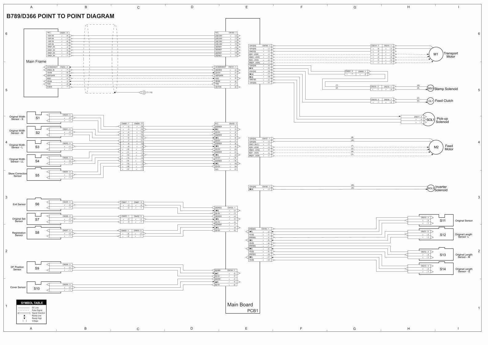
D037/D038/D040/D041 POINT TO POINT DIAGRAM (1/2)
Laser Synchronizing Detector -KC
Laser Synchronizing Detector -YM

PSU 2/2
BCU (2/2)
-11
-12
-13
-14
-15
-16
Ver
tical
Tra
nspo
rt Se
nsor
1:G
ND
Ver
tical
Tra
nspo
rt Se
nsor
1: O
UTP
UT
Verti
cal T
rans
port
Sen
sor 1
: +5V
Ver
tical
Tra
nspo
rt S
enso
r 2: G
ND
Ver
tical
Tra
nspo
rt Se
nsor
2: O
UTP
UT
Verti
cal T
rans
port
Sens
or 2
: +5V
-9 -10
Rig
ht L
ower
Doo
r Ope
n Sw
itch:
GN
DR
ight
Low
er D
oor O
pen
Switc
h: O
UTP
UT
CN219
-3 -2 -1-4
CN1
M14
Pap
er F
eed
Mot
or: T
2-3 -2 -1-4
CN2
M15
Pap
er F
eed
Mot
or: T
1
Pap
er F
eed
Mot
or: T
2:A
SER
IES
Pape
r Fee
d M
otor
: T2:
/A S
ERIE
SP
aper
Fee
d M
otor
: T2:
B S
ERIE
SPa
per F
eed
Mot
or: T
2: /B
SER
IES
Pap
er F
eed
Mot
or: T
1:A
SER
IES
Pap
er F
eed
Mot
or: T
: /A
SE
RIE
SP
aper
Fee
d M
otor
: T1:
B S
ERIE
SPa
per F
eed
Mot
or: T
1: /B
SER
IES
-1 -2 -3 -4 -7 -8-5 -6
CN816
-19
-20
-21
JCN829CN829
ITB
Rot
atio
n S
enso
r:パ
ルス
ITB
Rot
atio
n Se
nsor:
+5V
ITB
Rot
atio
n S
enso
r:G
ND
-17
-18
-22
-23
-24
-25
-26
-27
-28
-29
-30
-31
-32
-33
-34
-35
-36
-3 -2 -1-4-5-6-7-8-9-10
-11
-12
-13
-14
-15
-16
-17
-18-1-2-3-4-5-6-7-8
JCN816
CN2
-3 -2 -1
S10CN3
-3 -2 -1
CN1
SW2
Rig
ht L
ower
Doo
r Ope
n S
witc
h-2 -1
CN816
-1 -2 -3 -4 -5 -6 -7 -8
CN829
ITB Unit 1/2
CN1
M16
-1-2-3-4-5-6-7-8-9-10
-11
-12
-13
-14
-15
-4 -5 -6 -7 -8 -9 -10
-11
-12
-13
-14
-15
-16
-17
-18
-2 -3-1
CN2
-3 -2 -1IT
B R
otat
ion
Sen
sor
S12
N.C
.N
.C.
IBT
MT:
Enc
oder
CLK
IBT
MT:
FB_O
N/O
FF
IBT
MT:
CLK
IBT
MT:
GA
IN
IBT
MT:
BR
AKE
IBT
MT:
CW
/CC
WIB
T M
T:ST
OP
/STA
RT
IBT
MT:
/LO
CK
IBT
MT:
+5V
IBT
MT:
GN
DIB
T M
T:G
ND
IBT
MT:
GN
DIB
T M
T:+2
4VS
2IB
T M
T:+2
4VS
2
IBT
MT:
FG_C
LK
Verti
cal T
rans
port
Sen
sor 1
ITB Unit Motor
-3-2-1 -4
CN226
+24V
S3+2
4V3
+24V
S2+2
4V2
CN
1
CN
2-2 -1-2 -1
Inte
rlock
Sw
itch
Inte
rlock
Sw
itch
PTR
Con
tact
Sen
sor:
GN
DP
TR C
onta
ct S
enso
r: O
UTP
UT
PTR
Con
tact
Sen
sor:
+5V
CN232
CN3
SW4
Dup
lex
Uni
t Ope
n S
witc
hD
uple
x U
nit O
pen
Switc
h:G
ND
Dup
lex
Uni
t Ope
n S
witc
h: O
UTP
UT
-3 -4 -5
CN2
-3 -2 -1
S19
PTR
Con
tact
Sen
sor
-2 -1-1 -2
CN848JCN1CN1
-3 -2 -1-2-1 -3
RFID-RWPCB15
CN234
CN823JCN823CN823
CN750
N.C
.
CN1
-3 -2 -1
S21
Tone
r End
Sen
sor:
Y
CN2
-3 -2 -1
S22
Tone
r End
Sen
sor:
M
CN3
-3 -2 -1
S23
Tone
r End
Sen
sor:
C
CN4
-3 -2 -1
S24
Tone
r End
Sen
sor:
K
RFI
D: G
ND
RFI
D: +
5VR
FID
: TX
D(B
CU
->R
FID
)R
FID
: RX
D(R
FID
->B
CU
)R
FID
: RES
ETR
FID
: GN
D
-3 -2 -1-4-5-6
-6 -13
-14
-16
-15
-17
-18
-19
-20
-21
-22
-23
-24
-8-7 -9 -10
-11
-12
Tone
r End
Sen
sor:
K: G
ND
Tone
r End
Sen
sor:
K: O
UTP
UT
Tone
r End
Sen
sor:
K: +
5VTE
Tone
r End
Sen
sor:
C: G
ND
Tone
r End
Sen
sor:
C: O
UTP
UT
Tone
r End
Sen
sor:
C: +
5VTE
Tone
r End
Sen
sor:
M: +
5VTE
Tone
r End
Sen
sor:
M: G
ND
Tone
r End
Sen
sor:
M: O
UTP
UT
Tone
r End
Sen
sor:
Y: G
ND
Tone
r End
Sen
sor:
Y: O
UTP
UT
Tone
r End
Sen
sor:
Y: +
5VTE
IC C
hip:
RFI
D
IC C
hip:
RFI
D
IC C
hip:
RFI
D
IC C
hip:
RFI
D-1-2-3-4-5-6
-7 -9-8 -10
-11
-12
CN5
-3 -2 -1
S20
ITB
Con
tact
Sen
sor
-3 -4 -5-9 -8 -7
ITB
Con
tact
Sen
sor:
GN
DIT
B C
onta
ct S
enso
r: O
UTP
UT
ITB
Con
tact
Sen
sor:
+5V
N.C
.N
.C.
-2-1-2-1 -3 -1
4-1
5
-17
-16
-18
-19
-20
-21
-22
-23
-24
-13
-23
-22
-21
-24
-15
-14
-13
-16
-17
-18
-19
-20
-5-4 -6
-12
-11
-10
-1-2-3-4-5-6-7-8-9-10
-11
-12
CN849JCN849CN849
-7 -9-8 -10
-11
-12
-5-4 -6-2-1 -3
Side Tray
-12
-13
-14
-15
-16
-17
-18
-19
-20
-21
-22
CN840JCN840
CN5
M20
Fusi
ng/ P
aper
Exi
t Mot
or:C
LKFu
sing
/ Pap
er E
xit M
otor
:BR
AKE
Fusi
ng/ P
aper
Exi
t Mot
or:C
W/C
CW
Fusi
ng/ P
aper
Exi
t Mot
or:S
TOP
/STA
RT
Fusi
ng/ P
aper
Exi
t Mot
or:/L
OC
KFu
sing
/ Pap
er E
xit M
otor
:+5V
Fusi
ng/ P
aper
Exi
t Mot
or:G
ND
Fusi
ng/ P
aper
Exi
t Mot
or:G
ND
Fusi
ng/ P
aper
Exi
t Mot
or:G
ND
Fusi
ng/ P
aper
Exi
t Mot
or:+
24V
S3Fu
sing
/ Pap
er E
xit
Mot
or:+
24V
S3
CN235
-1 -2 -3 -4 -5 -6 -7 -8 -9 -10
-11
Side
Tra
y:S
ide
Tray
Mot
or: C
UR
N.C
.
Side
Tra
y:+5
VS
ide
Tray
:GN
D
Side
Tra
y: S
et S
witc
h
Sid
e Tr
ay:+
24V
4S
ide
Tray
:GN
D
Side
Tra
y:S
ide
Tray
Mot
or:E
NB
Sid
e Tr
ay:S
ide
Tray
Mot
or: C
LK
Side
Tra
y: E
xit S
enso
rSi
de T
ray:
Junc
tion
Gat
e S
OL
CN150
CN100
-1-2-3-4-5-6-7-8-9-10
-11
-1-2-3-4-5-6-7-8-9-10
-11
-1 -2 -3 -4 -5 -6 -7 -8 -9 -10
-11
-1-2-3-4-5-6-7-8-9-10
-11
Fusi
ng/ P
aper
Exi
t Mot
or 1 Bin Tray
Pape
r Exi
t Sen
sor:
GN
DPa
per E
xit S
enso
r: O
UTP
UT
Pap
er E
xit S
enso
r: +5
V
CN819
CN227
JCN819
1 B
in T
ray:
+5VE
1 Bi
n Tr
ay:+
5V
1 Bi
n Tr
ay:G
ND
1 B
in T
ray:
Pap
er S
enso
r1
Bin
Tra
y: C
onne
ct S
enso
r
1 B
in T
ray:
Exi
t Sen
sor
1 Bi
n Tr
ay: I
nver
ter M
otor
-1 -2 -3 -4 -5 -6 -7
Junc
tion
Gat
e S
olen
oid:
+24V
S3Ju
nctio
n G
ate
Sol
enoi
d: C
ON
TRO
L
Inve
rter S
enso
r: G
ND
Inve
rter S
enso
r: O
UTP
UT
Inve
rter S
enso
r: +5
V
-14
-13
-12
-16
-15
-17-8-9-10
-11 -5-6-7 -21
-22
-18
-19
-20
-13
-12
-16
-15
-14
-17
-18
-19
-20
-21
-22
Inve
rter M
otor
: A S
ERIE
SIn
verte
r Mot
or: /
A S
ERIE
SIn
verte
r Mot
or: B
S
ER
IES
Inve
rter M
otor
: /B
SER
IES
-8 -9 -10
-11
Inve
rter M
otor
CN1
M21
-8 -9 -10
-11
-2-3 -1-4
Fusi
ng F
ront
Sen
sor:
GN
DFu
sing
Fro
nt S
enso
r: O
UTP
UT
Fusi
ng F
ront
Sen
sor:
+5V
CN500
CN550
CN4
S26CN5
S27JCN839CN839
CN819
CN3
S25CN2JCN2
Junc
tion
Gat
e So
leno
id
CN
1 2
Paper Exit Unit
SOL1-3 -2 -1-4-5-6-7
-3 -2 -1-4-5-6-7
-3-2-1 -4 -5 -6 -7
-3-2-1 -4 -5 -6 -7
-2-3 -1-4
-13
-12
-16
-15
-14
-17
-18
-19
-20
-21
-22
-2 -1 -2-3 -1 -2-3 -1 -2-3 -1
Inve
rter S
enso
r
Fusi
ng F
ront
Se
nsor
Pape
r Exi
t Se
nsor
*Exclusive against Finisher
F8
Con
trolle
r Box
Fa
n
CN228
-2 -3-1
Con
trolle
r Box
Fan
:/LO
CK
Con
trolle
r Box
Fan
: CO
NTR
OL
Con
trolle
r Box
Fan
:GN
D
CN828JCN828
CN
2 31-2-3 -1
Junc
tion
Gat
e Fa
n
F9
-2 -3-1
CN850JCN850
CN
2 31Ju
nctio
n G
ate
Fan:
+24
V3Ju
nctio
n G
ate
Fan:
LO
CK
Junc
tion
Gat
e Fa
n: C
ON
TRO
L
CN238
-2-3 -1
CN229
-4 -3 -2 -1-8 -7 -6 -5-12
-11
-10 -9-13
-14
-15
-19
-18
-17
-16
-23
-22
-21
-20
-24
HVP:CBPCB17
CN950
-1 -2 -3 -4 -5 -6 -7 -8 -9 -10
-11
-12
-13
-14
-15
-16
-17
-18
-19
-20
-21
-22
-23
-24
C4(Charge: Y) T44 T844
C3(Charge: M) T43 T843
C2(Charge: C) T42 T842
C1(Charge: K) T41 T841
B1(
Dev
elop
men
t Bia
s:K
)T8
5 1T5
1
B2(
Dev
elop
men
t Bia
s:C
)T8
5 2T5
2
B3(
Dev
elop
men
t Bia
s:M
)T8
5 3T5
3
B4(
Dev
elop
men
t Bia
s:Y
)T8
5 4T5
4
HV
P: +
24VS
2H
VP:
GN
DH
VP:
PW
M: C
harg
e: D
C: K
HV
P: P
WM
: Cha
rge:
DC
: CH
VP:
PW
M: C
harg
e: D
C: M
HV
P: P
WM
: Cha
rge:
DC
: YH
VP:
PW
M: C
harg
e: A
C: K
HV
P: P
WM
: Cha
rge:
AC
: CH
VP:
PW
M: C
harg
e: A
C: M
HV
P:PW
M: C
harg
e: A
C: Y
HV
P: T
riger
: C: F
requ
ency
Mod
ulat
ion
HV
P: P
WM
: Cha
re A
C_C
LK
HV
P: F
B: C
harg
e: A
C: K
HV
P: F
B: C
harg
e: A
C: C
HV
P: F
B: C
harg
e: A
C: M
HV
P: F
B: C
harg
e: A
C: Y
HV
P: P
WM
: Dev
elop
men
t B: Y
HV
P: P
WM
: Dev
elop
men
t B: M
HV
P: P
WM
: Dev
elop
men
t B: C
HV
P: P
WM
: Dev
elop
men
t B: K
HV
P: S
C: C
BH
VP:
GN
DH
VP:
+24
VS2
N.C
.
Drive Unit 2/2
HVP:TTSPCB16
-4 -3 -2 -1-8 -7 -6 -5-10 -9
HV
P: S
C: T
HV
P: P
WM
: ITB
: YH
VP:
PW
M: I
TB: M
HV
P: P
WM
: ITB
: CH
VP:
PW
M: I
TB: K
HV
P: P
WM
: PTR
: +H
VP:
PW
M: P
TR: -
HV
P: +
24VS
2H
VP:
GN
D
HV
P: F
B: P
TR: -
CN230
ITB Unit 2/2
TS(PTR)T60
TF1(ITB: K)T861 T61
TF3(ITB: M)T863 T63
TF4(ITB: Y)T864 T64
CN802
-1 -2 -3 -4 -5 -6 -7 -8 -9 -10
TF2(ITB: C)T862 T62
Toner Supply Unit
PTR Unit(2/2)
T860
*Standard for NA and EU.
ARDF
CN201 CN236
123456781 2 3 4 5 6 7 8 1 2 3 4 5 6 7 8 9
123456789
AR
DF:
GN
D
AR
DF:
+24
V4
AR
DF:
+24
V4
AR
DF:
+24
V4
AR
DF:
+24
V4
AR
DF:
GN
DA
RD
F: G
ND
AR
DF:
GN
D-1-2-3-4-5-6-7-8
AR
DF:
+5V
ESN
SA
RD
F: R
XD(D
F->B
CU
)A
RD
F: O
rigin
al L
eadi
ng E
dge
Det
ect
AR
DF:
TX
D(B
CU
->D
F)A
RD
F: D
FGAT
EA
RD
F: +
5VA
RD
F: G
ND
-1-2-3-4-5-6-7
CN CN
CN811 CN812
CN CN
-1 -2 -3 -4 -5 -6 -7 -8 -1 -2 -3 -4 -5 -6 -7 -8 -9
CN
CN
4321
1234
321 4K
ey C
ount
er-1-2-3-4
Key
Cou
nter
:GN
DK
ey C
ount
er: C
ard
Set
Sen
sor
Key
Cou
nter
:+24
VC
NT
Key
Cou
nter
: Cou
nt
CN217
CN
C3CN2CN3
CN1JCN1CN1
CN218
-1-2-3-4
-4-3-2-1
-1-2-3-4
-2-1-2-1
Mec
hani
cal
Cou
nter
: K
Mec
hani
cal
Cou
nter
: FC
Mec
hani
cal C
ount
er: K
:+24
VC
NT
Mec
hani
cal C
ount
er: K
: Cou
ntM
echa
nica
l Cou
nter
: FC
:+24
VC
NT
Mec
hani
cal C
ount
er: F
: Cou
nt
*NA only
C1C2
CN824
S28
CN237
-1 -3-2 -4
N.C
.
Ther
mop
ile: H
eatin
g Th
erm
opile
:GN
DTh
erm
opile
:+5V
-3-4 -1-2Th
erm
opile
CN212
CN2
CN1
JCN2
TD S
enso
r: Y:
SCL
TD S
enso
r: Y
:FB
TD S
enso
r: Y
:+5V
HST
TD S
enso
r: Y:
PWM
TD S
enso
r: Y:
SDA
TD S
enso
r: Y
:GN
D
TD S
enso
r: M
:SC
L
TD S
enso
r: M
:FB
TD S
enso
r: M
:+5V
HST
TD S
enso
r: M
:PW
MTD
Sen
sor:
M:S
DA
TD S
enso
r: M
:GN
D
TD S
enso
r: C
:SC
L
TD S
enso
r: C
:FB
TD S
enso
r: C
:+5V
HST
TD S
enso
r: C
:PW
MTD
Sen
sor:
C:S
DA
TD S
enso
r: C
:GN
D
TD S
enso
r: K:
SCL
TD S
enso
r: K
:FB
TD S
enso
r: K
:+5V
HST
TD S
enso
r: K:
PWM
TD S
enso
r: K:
SDA
TD S
enso
r: K
:GN
D
-A1
-A2
-A3
-A4
-A5
-A6
CN1
CN2CN2
CN1
TD Sensor: MS32
PCU_M
CN1
CN2
CN1
JCN2
CN1
CN2CN2
CN1
TD Sensor: CS33
PCU_C
CN1
CN2CN2
CN1
PCU_K
CN1
-A7
-A8
-A9
-A9
- A11
- A12
-B1
-B2
-B3
-B4
-B5
-B6
-B7
-B8
-B9
-B9
- B11
- B12
CN833 CN835
CN2JCN2
CN2JCN2
CN832 CN834
CN1
CN2CN2
CN1
TD Sensor: YS31
PCU_Y
-3-4-5-6 -2 -1 -3-4-5-6 -2 -1 -3-4-5-6 -2 -1 -3-4-5-6 -2 -1
-1 -3-2 -4 -5 -6 -1 -3-2 -4 -5 -6 -1 -3-2 -4 -5 -6 -1 -3-2 -4 -5 -6
-3-4-5-6 -2 -1-7-8 -3-4-5-6 -2 -1-7-8 -3-4-5-6 -2 -1-7-8 -3-4-5-6 -2 -1-7-8
-1 -3-2 -4 -5 -6 -7 -8 -1 -3-2 -4 -5 -6 -7 -8 -1 -3-2 -4 -5 -6 -7 -8 -1 -3-2 -4 -5 -6 -7 -8
-3-4-5-6 -2 -1 -3-4-5-6 -2 -1 -3-4-5-6 -2 -1 -3-4-5-6 -2 -1
-1 -3-2 -4 -5 -6
-1 -3-2 -4 -5 -6
-1 -3-2 -4 -5 -6
-1 -3-2 -4 -5 -6
-1 -3-2 -4 -5 -6
-1 -3-2 -4 -5 -6
-1 -3-2 -4 -5 -6
-1 -3-2 -4 -5 -6
CN2
S36
CN837
JCN837
CN1
Dru
m P
hase
S
enso
r: C
MY
-18
-17
-16
CN2
S35
CN836
JCN836
CN1
Dru
m P
hase
S
enso
r: K
-3-2-1
Dru
m P
hase
Sen
sor:
CM
Y:G
ND
Dru
m P
hase
Sen
sor:
CM
Y: O
UTP
UT
Dru
m P
hase
Sen
sor:
CM
Y:5
V
Dru
m P
hase
Sen
sor:
K:G
ND
Dru
m P
hase
Sen
sor:
K: O
UTP
UT
Dru
m P
hase
Sen
sor:
K:+5
V
CN220
CN1
M22
-4 -5 -6 -7 -8 -9 -10
-11
-12
-13
-14
-15
Dru
m/D
evel
opm
ent M
otor
:K:C
LKD
rum
/Dev
elop
men
t Mot
or:K
:BR
AKE
Dru
m/D
evel
opm
ent M
otor
: K:C
W/C
CW
Dru
m/D
evel
opm
ent M
otor
: K:S
TOP/
STA
RT
Dru
m/D
evel
opm
ent M
otor
: K:/L
OC
KD
rum
/Dev
elop
men
t Mot
or: K
:+5V
Dru
m/D
evel
opm
ent M
otor
: KG
ND
Dru
m/D
evel
opm
ent M
otor
: KG
ND
Dru
m/D
evel
opm
ent M
otor
: K:G
ND
Dru
m/D
evel
opm
ent M
otor
: K:+
24V
S2D
rum
/Dev
elop
men
t Mot
or: K
:+24
VS2
Dru
m/D
evel
opm
ent M
otor
:K:G
AIN
Dru
m M
otor
: CM
Y:C
LKD
rum
Mot
or: C
MY:
BRAK
ED
rum
Mot
or: C
MY
CW
/CC
WD
rum
Mot
or: C
MYS
TOP/
STA
RT
Dru
m M
otor
: CM
Y/L
OC
KD
rum
Mot
or: C
MY:
+5V
Dru
m M
otor
: CM
Y:G
ND
Dru
m M
otor
: CM
Y:G
ND
Dru
m M
otor
: CM
Y:G
ND
Dru
m M
otor
: CM
Y:2
4VS2
Dru
m M
otor
: CM
Y:+
24V
S2
Dru
m M
otor
: CM
Y:G
AIN
CN2
M23
-21
-22
-19
-20
-23
-24
-25
-26
-27
-28
-29
-30
-3 -2 -1-3-2-1
-3 -2 -1
-3 -2 -1
-3 -2 -1-3-2-1
-1-2-3-4-5-6-7-8-9-10
-11
-12 -1-2-3-4-5-6-7-8-9-10
-11
-12
Dru
m M
otor
: CM
Y
Dru
m/D
evel
opm
ent
Mot
or: K
S9S8
CN214
CN3 CN1
-7 -8 -9 -10
CN1
-3 -2 -1
S6
-1 -2 -3
Reg
istra
tion
Sen
sor:
GN
DR
egis
tratio
n Se
nsor
: OU
TPU
TR
egis
tratio
n S
enso
r: +5
V
CN818
CN818
-2 -1
Pape
r End
Sen
sor:
T2: G
ND
Pap
er E
nd S
enso
r: T2
: OU
TPU
T
Pape
r End
Sen
sor:
T1: G
ND
Pap
er E
nd S
enso
r: T1
: OU
TPU
T
Pap
er E
nd
Sen
sor:
T2
Pap
er E
nd
Sen
sor:
T1
CN2
-3 -2 -1
S7Fu
sing
Ent
ranc
e S
enso
r: G
ND
Fusi
ng E
ntra
nce
Sens
or: O
UTP
UT
Fusi
ng E
ntra
nce
Sen
sor:
+5V
-2 -1-2 -1
-2-1
-4 -5 -6
-1-2-3
CN843JCN1CN1
PTR
Uni
t(1/2
)-3-2-1
JCN818
-3-4-5-6-9 -7-8 -2 -1
-11
-12
-14
-13
-15
-16
-17
-18
-19
CN1
S5
ID S
enso
r: FB
_Pse
nsor
ID S
enso
r: FB
_Fro
ntID
Sen
sor:
LED
_Fro
nt
ID S
enso
r: LE
D_C
ente
r
ID S
enso
r: FB
_Cen
ter
ID S
enso
r: +5
V
ID S
enso
r: G
ND
ID S
enso
r: LE
D_R
ear
ID S
enso
r: FB
_Rea
r
CN814JCN814CN814
-10
-11
-12
-13
-14
-15
-16
-17
-18
-19
-10
-11
-13
-12
-14
-15
-16
-17
-18
-19
CN847
-3 -2 -1-4-5-6-7-8-9
JCN847CN847
-3 -2 -1-4-5-6-7-8-9-1 -3-2 -4 -5 -6 -7 -8 -9
-1 -3-2 -4 -5 -6 -7 -8 -9
CN2JCN2
CN851
-3 -2 -1-3-2-1
Reg
istra
tion
Sen
sor
Fusi
ng E
ntra
nce
Sens
or
ID S
enso
r
-17
-19
-18
-20
-21
-22
-23
-24
-25
-27
-26
-28
-29
-32
Dup
lex
Ent
ranc
e M
otor
:A S
ERIE
SD
uple
x En
tranc
e M
otor
: /A
SE
RIE
SD
uple
x En
tranc
e M
otor
: B
SE
RIE
SD
uple
x En
tranc
e M
otor
: /B
SER
IES
Dup
lex
Exit
Mot
or:A
SE
RIE
SD
uple
x E
xit M
otor
: /A
SE
RIE
SD
uple
x Ex
it M
otor
:B S
ER
IES
Dup
lex
Exi
t Mot
or: /
B S
ER
IES
CN221
CN817JCN817
-7 -9-8 -10
-11
-12
-13
-14
-1 -2 -3 -4 -5 -6 -15
-16
GN
DD
uple
x En
tranc
e Se
nsor
+5V
GN
DD
uple
x E
xit M
otor
+5V
-30
-31
-17
-18
-19
-20
-21
-23
-22
-24
-25
-26
-27
-28
-32
-31
-30
-29-3 -2 -1-4-5-6-7-8-14
-13
-12
-11
-10 -9-15
-16
-3 -2 -1
CN7
-3 -2 -1
S15 S16
Duplex Unit (Manual Feed)
CN817
-1 -3-2 -4 -5 -6 -7 -8
-3 -2 -1-4 -3 -2 -1-4
CN1 CN2
M17
Dup
lex
Entra
nce
Mot
or
M18
Duplex Exit
Motor
CN6
By-
pass
Mot
or-3 -2 -1-4
CN10
M19
CN2 CN3
-3 -2 -1
S13 S14
-3 -2 -1-6 -5 -4
CN3
-1 -3-2 -4 -5 -6 -7 -8
-6-7-8 -4-5 -3 -2 -1
-3 -2 -1
CN8
S17 S18CN9
-3 -2 -1
JCN3CN1
-9 -10
-11
-12
-13
-14
-15
-16
-17
-18
-19
-20
-21
-22
-23
-24
-25
-26
-27
-28
-29
-30
-31
-32
By-
pass
Pap
er
Leng
th S
enso
r
By-p
ass
Pape
r En
d S
enso
rB
y-pa
ss H
P S
enso
rD
uple
x En
tranc
e S
enso
r
Dup
lex
Exit
Mot
or
By-
pass
Pap
er
Siz
e S
enso
r
By-
pass
Pap
er S
ize
Sen
sor:
MN
U_C
N2
By-
pass
Pap
er S
ize
Sen
sor:
MN
U_C
N1
By-
pass
Pap
er S
ize
Sen
sor:
GN
D
By-
pass
Pap
er S
ize
Sen
sor:
MN
U_C
N4
By-
pass
Pap
er S
ize
Sen
sor:
MN
U_C
N3
By-p
ass
Pape
r Len
gth
Sen
sor:
GN
DB
y-pa
ss P
aper
Len
gth
Sens
or: O
UTP
UT
By-
pass
Pap
er L
engt
h Se
nsor
: +5V
By-p
ass
Pape
r End
Sen
sor:
GN
DB
y-pa
ss P
aper
End
Sen
sor:
OU
TPU
TB
y-pa
ss P
aper
End
Sen
sor:
+5V
By-
pass
HP
Sen
sor:
GN
DB
y-pa
ss H
P Se
nsor
: OU
TPU
TBy
-pas
s H
P S
enso
r: +5
V
By-
pass
Mot
or: A
SER
IES
By-
pass
Mot
or: /
A S
ERIE
SB
y-pa
ss M
otor
: B
SER
IES
By-
pass
Mot
or: /
B S
ERIE
S
-15
-16
-18
-17
CN1
S37
Tem
pera
ture
/Hum
idity
Sen
sor:+
5VTe
mpe
ratu
re/H
umid
ity S
enso
r:Hum
idity
Det
ect
Tem
pera
ture
/Hum
idity
Sen
sor:G
ND
Tem
pera
ture
/Hum
idity
Sen
sor:
Tem
pera
ture
Det
ect
CN222
CN3
M24
-1-2-3-4-5-6-7-8-9-10
-11
Dev
elop
men
t Mot
or: C
MY
:CLK
Dev
elop
men
t Mot
or: C
MY:
BRA
KED
evel
opm
ent M
otor
: CM
Y:C
W/C
CW
Dev
elop
men
t Mot
or: C
MY:
STO
P/S
TAR
TD
evel
opm
ent M
otor
: CM
Y:/L
OC
KD
evel
opm
ent M
otor
: CM
Y:+5
VD
evel
opm
ent M
otor
: CM
YGN
DD
evel
opm
ent M
otor
: CM
Y:G
ND
Dev
elop
men
t Mot
or: C
MY
:GN
DD
evel
opm
ent M
otor
: CM
Y:+2
4VS2
Dev
elop
men
t Mot
or: C
MY
:+24
VS2
-1-2D
evel
opm
ent C
lutc
h:
K:+
24V3
Dev
elop
men
t Clu
tch:
K:
OFF
/ON
CN
MC1
Dev
elop
men
t C
lutc
h: K
1 2
CN830
JCN830
-3 -4 -5 -6 -7 -8 -9 -10
-11
-12
-13
Drive Unit /2
-1 -2
CN150
CN841JCN841
-19
-20
-21
-22
-23
-24
-25
-26
-14
N.C
.
-7-8 -5-6 -3-4 -1-2-9-1 -2 -3 -4 -5 -6 -7 -8 -9
CN100
CN838JCN838CN838
-3 -2 -1-4
-3-2-1 -4
Shi
ft Tr
ay:G
ND
Shi
ft Tr
ay:+
5VSh
ift T
ray:
Set
Sw
itch
Shift
Tra
y: P
ositi
on D
etec
tor
Shift
Tra
y:M
otor
:DIB
Shift
Tra
y:M
otor
:DIA
Shi
ft Tr
ay:G
ND
Shift
Tra
y:+2
4V3
Only for D038/D041
<Inner Shift Tray>
* Only for D038/D041
-3 -2 -1-4 -7-8 -5-6 -3-4 -1-2
Dev
elop
men
t Mot
or:
CM
Y
* Exclusive against FinisherTem
pera
ture
/Hum
idity
S
enso
r
ITB
Ton
er C
olle
ctio
n B
ottle
Ful
l Sen
sor
SW6CN1
SW7CN2
-19
-20
-11
-12
-13
-14
-15
-16
-17
-18
Pap
er S
ize
Sw
itch:
T1:
SIZ
E1_C
N2
Pap
er S
ize
Sw
itch:
T1:
SIZ
E1_C
N1
Pap
er S
ize
Sw
itch:
T1:
GN
D
Pape
r Siz
e Sw
itch:
T1:
SIZ
E1_C
N4
Pap
er S
ize
Sw
itch:
T1:
SIZ
E1_C
N3
Pape
r Siz
e Sw
itch:
T2:
SIZ
E2_C
N2
Pape
r Siz
e Sw
itch:
T2:
SIZ
E2_C
N1
Pap
er S
ize
Sw
itch:
T2:
GN
D
Pape
r Siz
e Sw
itch:
T2:
SIZ
E2_C
N4
Pape
r Siz
e Sw
itch:
T2:
SIZ
E2_C
N3
-1 -2 -3 -4 -5 -6 -7 -8 -9
CN4
S29
ITB
Tone
r Col
lect
ion
Bottl
e Fu
ll S
enso
r:GN
DIT
B To
ner C
olle
ctio
n B
ottle
Ful
l Sen
sor:O
UTP
UT
ITB
Ton
er C
olle
ctio
n B
ottle
Ful
l Sen
sor:+
5V
-10
CN822JCN822CN822
IBT
Tone
r Col
lect
ion
Bottl
e S
et S
witc
h: G
ND
IBT
Tone
r Col
lect
ion
Bot
tle S
et S
witc
h: O
UTP
UT
PCU
Ton
er C
olle
ctio
n Bo
ttle
Full
Sen
sor:G
ND
PCU
Ton
er C
olle
ctio
n Bo
ttle
Full
Sens
or: O
UTP
UT
PC
U T
oner
Col
lect
ion
Bot
tle F
ull S
enso
r: +5
V
PC
U T
oner
Col
lect
ion
Bot
tle F
ull S
witc
h:G
ND
PCU
Ton
er C
olle
ctio
n Bo
ttle
Full
Switc
h:O
UTP
UT
-3-4-5-6-7-8 -2 -1
CN815JCN815CN815
CN211
-3-4-5-6-9 -7-8 -2 -1-10
-1 -3-2 -4 -5 -6 -7 -8 -9 -10
CN842
CN2
S30CN1
SW5
PC
U T
oner
Col
lect
ion
Bot
tle S
et S
witc
h
JCN842CN842
-1 -3-2 -4 -5P
CU
Ton
er C
olle
ctio
n B
ottle
Ful
l Sen
sor
-3 -2 -1 -3 -2 -1-2 -1
-1 -2 -3 -4 -5 -6 -7 -8
-3-4-5 -2 -1 -3-4-5 -2 -1 -3-4-5 -2 -1
Pape
r Siz
e S
witc
h:
T1 Pape
r Siz
e Sw
itch:
T2
CN827 (Drawer)
CN233
CN826
CN1CN2
Hea
ting
Rol
ler T
herm
isto
r: E
nds:
Atm
osph
ere
Fusi
ng U
nit:
GN
D
-3-4-5-6-7-8-9-10
-11
-12
-13
-1 -3-2 -4 -5 -6 -7 -8 -9 -10
-11
CN5 CN4JCN5 JCN4CN CN
Fusing Unit
Fusi
ng U
nit:
Pape
r Siz
e Ty
pe D
etec
t1:1
00V
Ser
ies
Fusi
ng U
nit:
GN
D
Fusi
ng U
nit:
Pape
r Siz
e Ty
pe D
etec
t2:2
00V
Ser
ies
Pres
sure
Rol
ler T
herm
isto
r: C
ente
r
Fusi
ng U
nit:G
ND
Pres
sure
Rol
ler T
herm
isto
r 1: E
nds
Fusi
ng U
nit:
GN
D
Fusi
ng T
herm
isto
r: H
eatin
g: E
nds
Fusi
ng U
nit:
GN
D
-1 -3-2 -4 -5 -6 -7 -8 -9 -10
-11
Hea
ting
Rol
ler T
herm
isto
r
1 2
-1-2
Pres
sure
Rol
ler T
herm
isto
r 2 (E
nds)
-12
-13
1 2 3 4
CN3JCN3CN
1 2
Pres
sure
Rol
ler T
herm
isto
r 1 (C
ente
r)
TH TH TH
For 1
00V
ser
ies
For 2
00V
ser
ies
-1-2-3-4
TH
-1-2 -1-2-3
CN904
Hea
ting
Rol
ler F
usin
g La
mp:
Cen
ter_
N
Hea
ting
Rol
ler F
usin
g La
mp_
L
CN905
Hea
ting
Rol
ler F
usin
g La
mp:
End
s_N
N.C
.
-1 -5-3Pr
essu
re R
olle
r Fus
ing
Lam
p_N
Pre
ssur
e R
olle
r Fus
ing
Lam
p_L
Pre
ssur
e R
olle
r Fus
ing
Lam
p:C
ente
r(70
0W)
Pres
sure
Rol
ler F
usin
g La
mp(
420W
)
-2
-3-5 -6-4-1-2
-3-5 -6-4-1-2
Pre
ssur
e R
olle
r Fus
ing
Lam
p:E
nds(
500W
)
-1 -2
N.C
.-4
* * *
Ther
mos
tat
Ther
mos
tat
Ther
mos
tat
T HT H
T H
TD Sensor: KS34
D039 5282
D039 5343
D039 5288 D039 6240D039 2644
D039 2945 D039 6124
D039 2743
D039 4552 D039 6351 D041 5325
D039 5324
D039 5312 (3/3)
D039 5312 (2/3)D039 5310
D039 5253 D039 5318 2/2D040 5319 2/2
D039 5898D039 5280D039 5280D039 5286 D039 5286 D039 5286 D039 5286
D039 3085 D039 3085 D039 3085 D039 3085
D039 3575 D039 3575 D039 3575 D039 3575
D039 5340 (2/2) D039 5341(2/2)
D039 6592
D039 5272
D039 6115
D039 5270
D039 5271
D041 5290
D041 5291
D039 4301
D039 5202 (3/3)D040 5202 (3/3)
D039 4991
S11
Verti
cal T
rans
port
Sens
or 2
CN1
-3 -2
CN2
JCN2
-2-1
D039 2946
D039 4908
A
B
C
D
E
F
G
1 2 3 4 5 6 7 8 9 10
A
B
C
D
E
F
G
1 2 3 4 5 6 7 8 9 10
SW3
L2 L3
TS1
L4
TS2
TH1 TH2 TH3
D037/D038/D040/D041 POINT TO POINT DIAGRAM (2/2)
D039 4908

d037v301
Fig-1
9
12 3 4
56
8
10
7
6
3
1098
75
4
2
1
11
d037v302 Fig-2
12
2
1
3
4
5
67
Fig-3
89
10
d037v303 Fig-4d025V104
3
7
12
6
8
45
91011
121314
89
12
3
4
5
67
Fig-5 d037V305
123
5 4
Fig-7 d037v307
67891011
51 2 3 4
6789
10
Fig-8 d037v308
1112
4
Fig-6
3
12
1098
21
d037V306
567
11

1 2
34
56
7
Fig-9d037v309
5
Fig-10 d037v310
12
34
6
7
8
Symbol IndexNo.
Description P to P Page
M1 F 1-7 Scanner Motor C10 1/2M2 F 5-2 ITB Contact Motor F6 1/2M3 F 6-4 Toner Supply Motor:K F7 1/2M4 F 6-3 Toner Supply Motor:C F7 1/2M5 F 6-2 Toner Supply Motor:M F7 1/2M6 F 6-1 Toner Supply Motor:Y F7 1/2M7 F 6-9 Toner Collection Motor F8 1/2M8 F 7-1 Registration Motor F8 1/2M9 F 5-8 PTR Contact Motor F9 1/2M10 F 4-14 WTL Positioning Motor-Y F9 1/2M11 F 4-12 WTL Positioning Motor-M F9 1/2M12 F 4-11 WTL Positioning Motor-C F10 1/2M13 F 4-10 Polygon Mirror Motor F9 1/2M14 F 7-2 Paper Feed Motor: T1 A2 2/2M15 F 7-3 Paper Feed Motor: T2 A2 2/2M16 F 5-4 ITB Unit Motor B3 2/2M17 F 3-3 Duplex Entrance Motor A4 2/2M18 F 3-4 Duplex Exit Motor A4 2/2M19 F 3-5 By-pass Motor A5 2/2M20 F 9-7 Fusing/ Paper Exit Motor B7 2/2M21 F 4-2 Inverter Motor A9 2/2M22 F 9-6 Drum Motor: K F7 2/2M23 F 9-4 Drum Motor: CMY F8 2/2M24 F 9-3 Development Motor: K F8 2/2
MC1 F 9-5 Development Clutch: K F8 2/2
SOL1 F 4-4 Junction Gate Solenoid A9 2/2
SW1 F 2-9 Main Switch D1 1/2SW2 F 7-5 Right Lower Door Open Switch B3 2/2SW3 F 2-8 Interlock Switch B5 2/2SW4 F 3-2 Duplex Unit Open Switch B6 2/2SW5 F 6-10 PCU Toner Collection Bottle Set
SwitchE4 2/2
SW6 F 7-9 Paper Size Switch: T1 F4 2/2SW7 F 7-11 Paper Size Switch: T2 F4 2/2
L1 F 1-1 Exposure Lamp B9 1/2L2 Heating Roller Fusing Lamp: E1 2/2L3 Heating Roller Fusing Lamp: E2 2/2L4 F 8-5 Pressure Roller Fusing Lamp E2 2/2
Motors
Clutches
Solenoids
Switches
F 8-4
Lamps
Symbol IndexNo. Description P to P Page
S1 F 1-7 Original Length Sensor 1 C9 1S2 F 1-8 Original Length Sensor 2 C9 1S3 F 1-2 Scanner HP Sensor C9 1S4 F 1-5 Platen Cover Sensor C9 1S5 F 5-7 ID Sensor A1 2S6 F 7-4 Registration Sensor A1 2S7 F 5-6 Fusing Entrance Sensor A1 2S8 F 7-8 Paper End Sensor: T1 A2 2S9 F 7-10 Paper End Sensor: T2 A2 2S10 F 7-6 Vertical Transport Sensor 1 B2 2S11 F 7-7 Vertical Transport Sensor 2 A3 2S12 F 5-5 ITB Rotation Sensor B3 2S13 F 3-7 By-pass Paper Size Sensor A4 2S14 F 3-6 By-pass Paper Length Sensor A5 2S15 F 3-9 By-pass Paper End Sensor A5 2S16 F 3-8 By-pass HP Sensor A5 2S17 F 3-1 Duplex Entrance Sensor A5 2S18 F 3-10 Duplex Exit Motor A5 2S19 F 5-9 PTR Contact Sensor B6 2S20 F 5-3 ITB Contact Sensor B6 2S21 F 6-5 Toner End Sensor: Y A7 2S22 F 6-7 Toner End Sensor: M A7 2S23 F 6-6 Toner End Sensor: C A7 2S24 F 6-11 Toner End Sensor: K A7 2S25 F 4-5 Inverter Sensor A9 2S26 F 4-6 Fusing Exit Sensor A10 2S27 F 4-1 Paper Exit Sensor A10 2S28 F 8-2 Thermopile F3 2
S29 F 5-1 ITB Toner Collection Bottle FullSensor E4 2
S30 F 6-8 PCU Toner Collection Bottle FullSensor E4 2
S31 F 8-12 TD Sensor: Y E5 2S32 F 8-11 TD Sensor: M E5 2S33 F 8-10 TD Sensor: C E6 2S34 F 8-9 TD Sensor: K E6 2S35 F 9-1 Drum Phase Sensor: K F6 2S36 F 9-2 Drum Phase Sensor: CMY F7 2S37 F 2-3 Temperature/Humidity Sensor F9 2
FAN1 F 2-4 PSU Fan 1 C1 1FAN2 F 2-5 PSU Fan 2 D1 1FAN3 F 2-7 Laser Unit Fan F7 1FAN4 F 2-11 Ventilation Fan: Front F8 1FAN5 F 2-12 Ventilation Fan: Rear F8 1FAN6 F 2-2 Fusing Rear Fan F9 1FAN7 F 2-10 Fusing Front Fan F9 1FAN8 F 2-1 Controller Box Fan B10 2FAN9 F 4-3 Junction Gate Fan B10 2
TS1 F 8-3 Thermostat - Heating Roller E2 2TS2 F 8-6 Thermostat - Pressure Roller E2 2TH1 F 8-1 Thermistor - Heating Roller E2 2TH2 F 8-8 Thermistor - Pressure Roller: End E3 2TH3 F 8-7 Thermistor - Pressure Roller: Cen E3 2
HDD1 F 10-3 HDD A10 1CC1 F 10-4 Choke Coil (EU only) D1 1
Others
Sensors
FANs
Symbol IndexNo.
Description P to P Page
PCB1 F 10-5 PSU C2 1/2PCB2 F 10-7 i-Controller B4 1/2PCB3 F 10-8 BCU C6 1/2PCB4 F 1-10 OPU B6 1/2PCB5 LCDC B7 1/2PCB6 OP-L B7 1/2PCB7 OP-R B7 1/2PCB8 Inverter:TFF B7 1/2PCB9 F 1-6 SBU B8 1/2PCB10 F 1-4 Lamp Stabilizer C9 1/2PCB11 F 4-13 Laser Synchronizing Detector - F9 1/2PCB12 F 4-7 Laser Synchronizing Detector - F9 1/2PCB13 F 4-8 LDB: KC G9 1/2PCB14 F 4-9 LDB: YM G9 1/2PCB15 F 6-12 RFID-RW B6 2/2PCB16 F 10-1 HVPS: TTS D7 2/2PCB17 F 10-2 HVPS: CB D8 2/2
H1 F 2-6 Tray Heater (Option) B1 1/2
H2 F 1-3 Anti-condensation Heater -Scanner (Option) B1 1/2
H3 - Optional Tray Heater (Option) C1 1/2
C1 Mechanical Counter: K D2 2C2 Mechanical Counter: FC D2 2C3 - Key Counter D2 2
PCBs
Heaters
Counters
F 1-10
F 10-6
��������� ������ ��� �����
� � � � � � �
�
�
�
�
�
� � � � � � �
�
�
�
�
�
���
���
���
���
���
���
��������������
��
� ��!"!�
"!�
"!
"!�
"!�
"!�
"!#
� ��!"!�
"!� $��%�!$�&'��()$*+
� �,�!"!�
"!�
���
���
�'')!�&-�./�+����
���
���
���
� ��!"!�
"!�
� �#!"!
"!�
"!�$*+� 0(.1"-�
$�&'��()
�'')�����
��
�2'��'�$�&'��()
$*+�� �,�!"!�3��45��6
"!�5���6
���
���
� �,!"!
"!�
"!�
� ��!"!
"!�
"!�
� ��!"!
"!�
"!�
� � !"!
"!�
"!�
*�(7(��&!$'����$��
*�(7(��&!+'�7�/$'����!"+
$��
*�(7(��&!+'�7�/$'����!"!�
$�
*�(7(��&!+'�7�/$'����!"!$
$��
� , !"!
"!�
"!�
� ,�!"!
"!�
"!�
� ,,!"!
"!�
"!�
*�(7(��&!�()�/$'����!"!$
*�(7(��&!�()�/$'����!"!++
$1'8!����'.�(��$'����
� �,�!"!
"!�
"!�
� �,�!"!
"!�
"!�
� �, !"!
"!�
"!�
��(�!����)
� �,�!"!�
"!�
"!
"!�
"!�
"!�
"!#
"!9
"!:
"�,
"��
"��
� ��5,6
3�45�6
� ��5,6
3�45�6
� ��5,6
3�45�6
� ��5,6
3�45�6
5��6
5��6
5��6
� �,�!"!�
"!�
"!
"!�
"!�
"!�
5,6� �
5��6
5�63�4
5,6� �
5�63�4
� �, !"!�
"!�
"!
"!�
"!�
"!�
"!#
"!9
"!:
5,6� ��
5�63�4
5,6� ��
5,6� ��
5�63�4
� �,#!"!�
"!�
"!
"!�
"!�
"!�
"!#
3��45��6
� �,9!"!�
"!�
"!
"!�
"!�
"!�
"!#
"!9
"!:
"�,
"��
"��
"!9
"!:
� �,�!"!�
"!�
"!
"!�
"!�
"!�
"!#
"!9
��(�!���%'� �,�!"!9 ��$��$;��
5,6� ��
5�63�4
<������
��$�
�<�
�<�
5�63�4�
��!!�=�=
=�=
3��4!
� ��>
3��4!
3��4!
3��4!
� ��>
� ��>
� ��>
� �,�!"!:
"!�
"!
"!�
"!�
"!�
"!#
"!9
"!�
"!�
"!
"!�
"!�
"!�
"!#
"!�
=�=
5��63��4
5,6� ��
5��63��4
5��63��4
5��63��4
5,6� ��
5,6� ��
5,6� ��
� �,,!"!�
"!�
"!
"!�
"!�
"!�
"!#
"!9
"!:
� �,,!"!�
"!�
"!
"!�
"!�
"!�
"!#
"!9
"!:
"�,
"��
"��
"!�
"!��
"��
"��
"�#
5,6� ��
5,6� ��
5��6
=�=
5,6� ��
5��6
5�63�4
5��6
5�63�4
5��6
5,6� ��
5�63�4
5��6
5�63�4
5,6� ��
=�=
5�63�4
� �,�!"!�
"!�
"!
"!�
"!�
"!�
"!#
"!9
"!:
"�,
"��
"��
"!�
"!��
"��
"��
"�#
� ,�!"!
"!�
"!�
*�(7(��&!�()�/$'����!"!�
� ,�!"!
"!�
"!�
*�(7(��&!�()�/$'����!"!+
� ,�!"!
"!�
"!�
�?(�!$'����
� ,�!"!
"!�
"!�
*�(7(��&!$'�$'����
� ,#!"!
"!�
"!�
�'7(�����(��$'����
5�63�4
5��6
5��6
5��6
� ,9!"!
"!�
"!�
��!0��(�(��$'����
� ,:!"!
"!�
"!�
��2'�!$'����
3��45��6
� �!�!� =�=�
�5��!�,@��6
��5��!�,@��6
�5��!�,@��6
��5��!�,@��6
3��45��6
3��45��6
� ��5,6
�5��!�,@��6
3��45��6
5���6
3��45��6
5���6
3��45��6
5���6
��5��!�,@��6
�5��!�,@��6
��5��!�,@��6
� ��5,6
��$��$;��
� ��>
3�4
<������
��$�
�<�
�<�
�4�
5��6
5��6
� �,,!"!�#
"!��
"!��
"!��
"!�
"!��
"!��
"!�,
"!:
"!9
"!#
"!�
"!�
"!�
"!
"!�
"!�
� �,�!"!�
"!�
"!
� �,�!"!�
"!�
"!
� �, !"!�
"!�
"!
0���
� ��!"!#
"!�
"!�
"!�
"!
"!�
"!�
� �,�!"!�
"!�
� ��!"!�
"!�
� ��!"!�
"!�
$�
$�
$�
$�
$
$�
$#
$9
$:
$�,
�������������!+(�'0-&�'!$(7��&$(7��&!�(�'.�(���'�)A!+�8�'�)A!(7/4�&��7'
��5!!!!!6

Symbol Name Index No. P-to-P
M1 Transport 15 I6M2 Feed 19 I4
S1 Original Width S 4 A4S2 Original Width M 3 A4S3 Original Width L 2 A4S4 Original Width LL 1 A4S5 Skew Correction 5 A3S6 Exit 9 A3S7 Original Set 8 A3S8 Registration 6 A2S9 DF Position 14 A2
S10 Cover 7 A1S11 Original 10 I3S12 Original Length L 13 I2S13 Original Length M 12 I2S14 Original Length S 11 I2
SOL1 Pick-up 17 H4SOL2 Inverter 18 H3SOL3 Stamp 21 H5
MC1 Feed 16 H5
PCB1 Main Board 20 E1-6PCBs
Motors
Sensors
Solenoids
Magnetic Clutches
B789D102.WMF
1
23
67
89
1011
4
5
1213
14
16 1715 18
19
20
B789D103.WMF
21

A
B
C
D
E
F
G
1 2 3 4 5 6 7 8 9 10
A
B
C
D
E
F
G
1 2 3 4 5 6 7 8 9 10
SGN
DLo
wer
PH
SN
2[5
]V
CC
(+5
V)
SG
ND
VC
C(+5
V)Lo
wer
PH
SN
1[5
]
SG
NDUp
per
PH
SN
2[5
]V
CC(
+5V)
SG
NDUp
per
PH
SN
1[5
]V
CC(
+5V)
CN
103-
1"
-2"
-3
"-4
"-5
"-6
"-7
"-8
"-9
"-1
0"
-11
"-1
2
BAN
K_C
OV
OP
[5]
SG
ND
VC
C(+5
V)
SGN
DF4
_LM
T[5
]VC
C(+5
V)
"-1
7"
-18
"-1
9
"-1
2"
-13
"-1
4
F4M
_UP
[24]
"-2
0
"-2
1
"-1
5
"-1
6
[24
24/0
]/B
+24
V[2
424
/0]/
A[2
424
/0]B
+24
V
[24
24/0
]A
VC
C(+
5V)
Lowe
rPF
Cl[
24
]
"-1
7
"-1
8
+24
V"
-13
"-1
4U
pper
PFCl
[24
]
Rela
yCl
utch
[24
]
"-1
5
"-1
6+2
4V
+24
V
CN1
02-1
"-2
"-3
"-4
"-5
"-6
"-7
"-8
"-9
SGN
D
VC
C(+5
V)XB
ANK
_RL
YS[5
]
SG
NDF4
_PE
[5]
VC
C(+5
V)
SGN
D
"-1
1"
-10
VCC(
+5V)
[5]
Uppe
rP.
Size
SN
1
Upp
erTr
aySe
t
"-6
"-2
"-3
"-4
"-5
CN1
01-1
CN10
4-1
"-2
"-3
"-4
"-5
"-6
"-7
"-8
"-9
"-1
3"
-14
"-1
5"
-16
"-1
7"
-18
"-1
9"
-20
"-2
1"
-22
"-2
3
"-2
7"
-28
SG
ND
+5V
[5]
Uppe
rP.
Size
SN
2S
GN
D
+5V
[5]
Uppe
rP.
Size
SN
3S
GN
D
+5V
+5V
Lowe
rTr
aySe
t+5
V
[5]
Lowe
rP.S
ize
SN
1S
GND
+5V
[5]
Low
erP.
Size
SN
2S
GND
+5V
[5]
Lowe
rP.
Size
SN
3S
GN
D
+5V
+5V
F3_
PE[5
]
F4M
_D
OW
N[2
4]
F3_L
MT
[5]
F3M
_UP
[24]
F3M
_DO
WN
[24]
CN100
To BiCU
Low
er P
aper
H
eigh
t Sen
sor 2
Low
er P
aper
H
eigh
t Sen
sor 1
Upp
er P
aper
H
eigh
t Sen
sor 2
Upp
er P
aper
H
eigh
t Sen
sor 1
S1 S2 S3 S4MC1 MC2 MC3
Upp
er P
aper
Fe
ed C
lutc
h
Rel
ay C
lutc
h
Low
er P
aper
Fe
ed C
lutc
h
S5 S6 S7
SW3Ver
tical
Tra
nspo
rt S
enso
r
Low
er P
aper
End
S
enso
r
Upp
er P
aper
End
S
enso
r Tray
Cov
er S
witc
h
S8M2
S9M3
Paper Tray Main Board (PCB1)
M1 S10 S11 S12 SW1 SW2S13 S14 S15Lo
wer
Lift
Sen
sor
Low
er L
ift M
otor
Upp
er L
ift S
enso
r
Upp
er L
ift M
otor
Pap
er F
eed
Mot
or
Upp
er P
age
Siz
e S
enor
2
Upp
er P
age
Siz
e S
enor
3
Upp
er T
ray
Set
S
WLo
wer
Pap
er
Siz
e S
enso
r 1Lo
wer
Pap
er
Siz
e S
enso
r 2
Low
er P
aper
S
ize
Sen
sor 3
Upp
er P
age
Siz
e S
enor
1
Low
er T
ray
Set
S
W
Pin No.A1A2A3A4A5A6A7A8A9A10A11A12A13A14A15
SignalF3_PEF4_PEF3_LMTF4_LMTXF3_RLYSXBANK_RLYSF3_SIZEF4_SIZEBANK_HIGHBANK_SETSCAN_ASCAN_BXF3_RLYCLXF3_FDCLXF4_FDCL
Pin No.B1B2B3B4B5B6B7B8B9B10B11B12B13B14B15
SignF3M_UPF3M_DNF4M_UP
High spdXBANK_MLD
GND+24VL+24VL+24VLGNDGNDGND
XBANK_MONF4M_DN
+5V
(CN100)
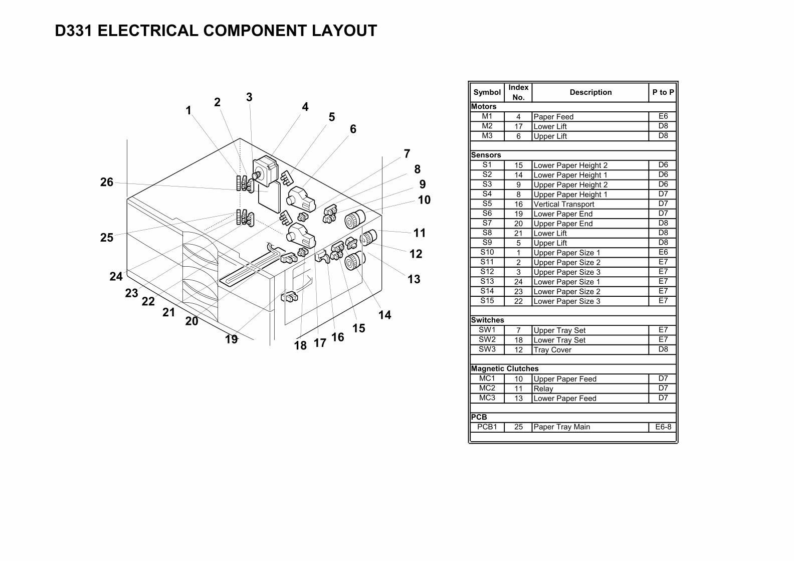
3 Symbol IndexNo. Description P to P
MotorsM1 4 Paper Feed E6M2 17 Lower Lift D8M3 6 Upper Lift D8
SensorsS1 15 Lower Paper Height 2 D6S2 14 Lower Paper Height 1 D6S3 9 Upper Paper Height 2 D6S4 8 Upper Paper Height 1 D7S5 16 Vertical Transport D7S6 19 Lower Paper End D7S7 20 Upper Paper End D8S8 21 Lower Lift D8S9 5 Upper Lift D8
S10 1 Upper Paper Size 1 E6S11 2 Upper Paper Size 2 E7S12 3 Upper Paper Size 3 E7S13 24 Lower Paper Size 1 E7S14 23 Lower Paper Size 2 E7S15 22 Lower Paper Size 3 E7
SwitchesSW1 7 Upper Tray Set E7SW2 18 Lower Tray Set E7SW3 12 Tray Cover D8
Magnetic ClutchesMC1 10 Upper Paper Feed D7MC2 11 Relay D7MC3 13 Lower Paper Feed D7
PCBPCB1 25 Paper Tray Main E6-8
d331v102a
1 2 45
6
78910
11
12
13
1415
1617181920
2122
2324
25
26
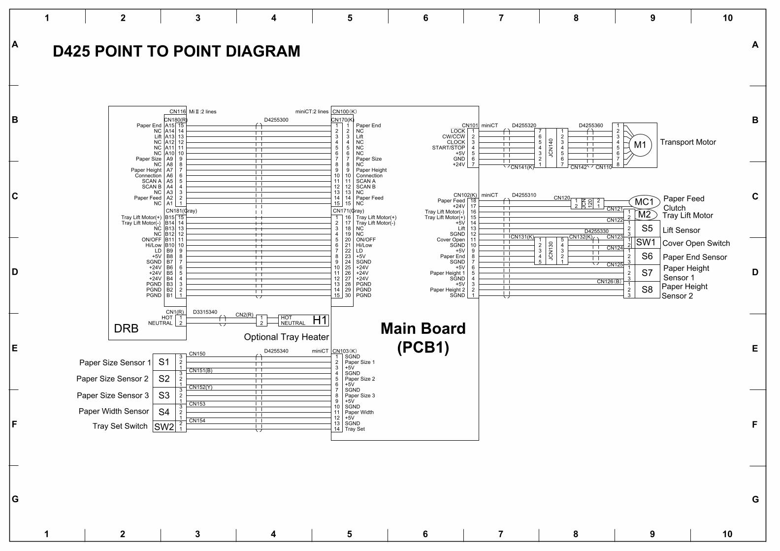
CN100(K)
Paper End
Lift
Paper Size
Paper HeightConnectionSCAN ASCAN B
Paper Feed
Tray Lift Motor(+)Tray Lift Motor(-)
ON/OFFHi/LowLD+5VSGND+24V+24V+24VPGNDPGNDPGND
CN101
CW/CCWCLOCK
START/STOP+5V
+5VPaper End
SGND
1110
1
98765432
+5VPaper Height 1
SGND+5V
Paper Height 2SGND
Cover OpenSGND
SGNDLift
+5VTray Lift Motor(+)Tray Lift Motor(-)
A15A14A13A12A11A10A9
CN116
A8A7A6A5A4A3A2A1
B15B14B13B12
B7
B10B9B8
B11
B6B5B4B3
B1B2
Paper End
Lift
Paper Size
Paper HeightConnection
SCAN ASCAN B
Paper Feed
Tray Lift Motor(+)Tray Lift Motor(-)
ON/OFFHi/Low
LD+5V
SGND+24V+24V+24V
PGNDPGNDPGND
123
S7123
S8
CN125
CN126(B)
CN110
Transport Motor
Paper Height Sensor 1Paper Height Sensor 2
D4255300123456
123456
miniCT
HOTNEUTRAL
CN1(R)HOTNEUTRAL
CN2(R)12
Optional Tray Heater
Paper Size Sensor 1
Paper Size Sensor 2
Paper Size Sensor 3
Paper Width Sensor
Tray Set Switch
Paper Width
Paper Size 1
Paper Size 2
Paper Size 3
D4255340
S1
S2
S3
S4
12345
14
6789
10111213
CN103(K)
SGND
SGND
SGND
SGND
SGND
Tray Set
+5V
+5V
+5V
+5V
SW2 21
321321321321
CN150
CN151(B)
CN152(Y)
CN154
miniCT
12
D3315340
M2
12
16151413
12123
S5
CN121
CN122Tray Lift Motor
Lift Sensor
D4255310
123
S6SW11
2CN123
CN124
Paper End Sensor
Cover Open Switch
CN102(K) miniCT
12345
14
6789
10111213
15
miniCT:2 lines
12345
14
6789
10111213
15
1415
16171819
28
2021222324252627
13121110987654321
2930
CN132(K)54321
12345 JC
N13
0
CN171(Gray)
CN170(K)
D4255330CN131(K)
CN153
121110
1
98765432
151413
121110
1
98765432
151413
MiⅡ:2 linesCN180(R)
CN181(Gray)
NC
NC
NC
NC
NC
NC
NCNC
NC
NC
NC
NC
NC
NC
NCNC
787
M1GND+24V
NCNC
1718Paper Feed
+24V MC112 1
2
JCN
120 Paper Feed
ClutchCN120
LOCKD4255320
CN142
54321
12345JC
N14
0
D4255360
CN141(K)67
67
A
B
C
D
E
F
G
1 2 3 4 5 6 7 8 9 10
A
B
C
D
E
F
G
1 2 3 4 5 6 7 8 9 10

d425v101
12
3
45
67
89
1011
1213
1415
Symbol IndexNo.
Description P to P
M1 5 Transport Motor B9M2 3 Tray Lift Motor C9
MC1 4 Paper Feed C9
SW1 6 Cover Open D9SW2 10 Tray Set F3
PCB1 1 Main Board E6
H1 12 Optional Tray Heater E4
S1 15 Paper Size 1 E3S2 14 Paper Size 2 E3S3 13 Paper Size 3 F3S4 9 Paper Width F3S5 2 Lift C9S6 11 Paper End D9S7 7 Paper Height 1 D9S8 8 Paper Height 2 D9
Heaters
Sensors
Motors
Clutches
Switches
PCBs

Junction Gate Unit
7654321
CN500AMP MINI CT 7P
+5V+5VE
1234567
Harness:D4265300
SGNDConnect Sensor
Paper Sensor1-Bin Tray Exit Sensor
Inverter Motor
CN550AMP CT 7P
12
CN551AMP MINI CT 2P
Anode
LED
21
Harness:D4265310
CN501MINI CT 2P
1-Bin Tray Control Board(PCB1)
123
456
CN552AMP CT(B) 3P
SGNDPaper Sensor
321
S1+5VE
SGND1-Bin Tray Exit Sensor
+5V
CN502AMP MINI CT 6P
CN553AMP CT 3P
321
S2
JCN550
1234567
+5V+5VESGNDConnect SensorPaper Sensor1-Bin Tray Exit SensorInverter Motor
Harness:D4265320
PCB2
A
B
C
D
E
F
G
1 2 3 4 5 6 7 8 9 10
A
B
C
D
E
F
G
1 2 3 4 5 6 7 8 9 10
Paper Sensor
1-Bin Tray Exit Sensor
LED Board
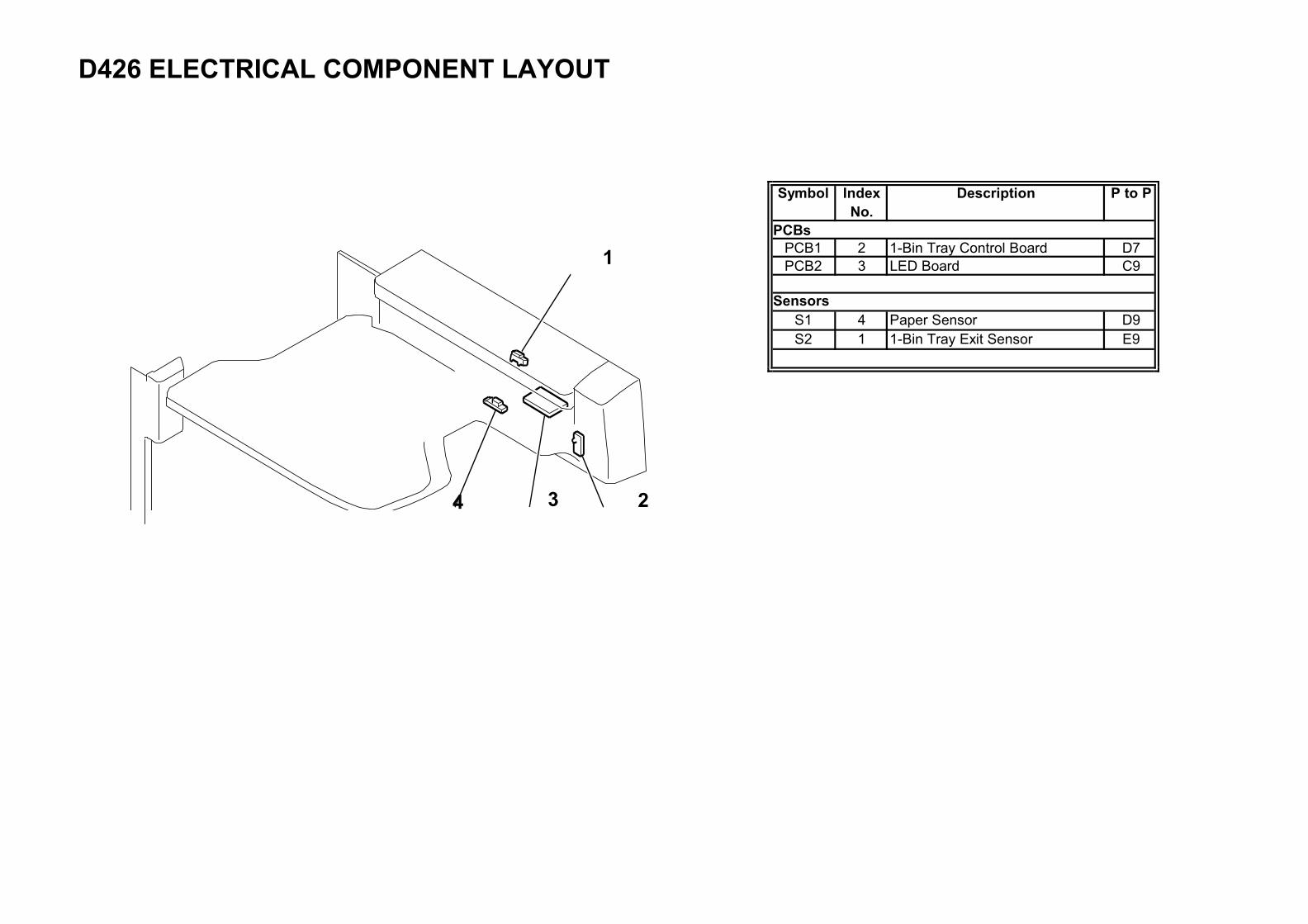
d426V101
3
1
24
Symbol IndexNo.
Description P to P
PCB1 2 1-Bin Tray Control Board D7PCB2 3 LED Board C9
S1 4 Paper Sensor D9S2 1 1-Bin Tray Exit Sensor E9
Sensors
PCBs

1110987654321
CN100AMP MINI CT 10P
MTENBMTCUR
123
456789
10
Harness:D4275300
SOLSide Tray Exit Sensor
Set Switch+5V
SGND
CN150AMP MINI CT 11P
1234
CN151AMP CT 4P
AAB
Harness:D4275310
CN101AMP MINI CT 4P
Side Tray Board
CN153AMP CT 3P
SGNDSide Tray Exit Sensor
321
S1+5V
CN103AMP MINI CT 3P
CN102AMP CT 2P
12
PGNDMTCLK
+24V
BBB
M14321
Side Tray Motor
123
+24VSOL
1110987654321
1234567891011
JCN150
NC
PGNDMTCLK
+24V
MTENBMTCURSOLSide Tray Exit SensorSet Switch+5VSGND SOL1 Side Tray Gate
Solenoid
Harness:D4275320
A
B
C
D
E
F
G
1 2 3 4 5 6 7 8 9 10
A
B
C
D
E
F
G
1 2 3 4 5 6 7 8 9 10
Side Tray Exit Sensor

3
12
4
d427V101
Symbol IndexNo.
Description P to P
M1 3 Side Tray Motor C9
SOL1 2 Side Tray Gate Solenoid D9
PCB1 4 Side Tray Board D6
S1 1 Side Tray Exit Sensor E9Sensors
Motors
Solenoid
PCBs

CN100AMP MINI CT 8P
MT+MT-
123456789
Position DetectorSet Switch
+5VSGND
12
CN151AMP CT 2P
Motor+
Harness: D4285310
CN101AMP MINI CT 2P
Half Turn Sensor Board
+24VPGND
Motor- M121
Tray Motor
Harness:D4285300
MT+MT-Position DetectorSet Switch+5VSGND
+24VPGND
123456789
987654321
JCN150
CN150AMP CT 9P
A
B
C
D
E
F
G
1 2 3 4 5 6 7 8 9 10
A
B
C
D
E
F
G
1 2 3 4 5 6 7 8 9 10

d428v101
1 2
Symbol IndexNo.
Description P to P
M1 1 Tray Motor C9
PCB1 2 Half Turn Sensor Board D7
Motors
PCBs

d429v201
12 3
45
6
7
8
9
101112
13
14
d429v202
1
23
4 56
78
9
1011
12
d429v203
1
23
d429v204
12
3 4
56
7
8
9
Fig 1 Fig 2
Fig 3 Fig 4
Symbol IndexNo.
Description
MotorsM1 F 1-10 Stapler Unit Movement MotorM2 F 1-11 Pick-Up Roller Contact MotorM3 F 1-5 Stapler MotorM4 F 1-2 Paper Transport MotorM5 F 1-3 Feed MotorM7 F 2-10 Front Jogger MotorM8 F 2-11 Rear Jogger MotorM6 F 1-12 Output Tray Motor
SensorsS1 F 1-6 Pick-up Roller HP SensorS4 F 2-4 Belt Roller Position SensorS2 F 1-4 Stapler Safety SensorS5 F 2-3 Stack Height Sensor 1S6 F 2-1 Stack Height Sensor 2S7 F 1-14 Tray Upper Limit SensorS8 F 1-13 Tray Lower Limit SensorS9 F 2-7 Jogger Unit Paper Sensor
S10 F 2-8 Front Jogger Fence HP SensorS11 F 2-6 Rear Jogger Fence HP SensorS3 F 1-8 Stapler Unit HP Sensor
S12 F 3-3 Entrance SensorS13 F 2-5 Relay Sensor
SwitchesSW1 F 1-9 Unit Open Switch
SolenoidsSOL1 F 2-9 Belt Roller SolenoidSOL2 F 2-12 Paddle Roller SolenoidSOL3 F 2-2 Stack Height Lever SolenoidSOL4 F 3-2 Inverter Junction Gate SolenoidSOL5 F 3-1 Inverter Roller Solenoid
PCBPCB1 F 1-1 Main Board
FANFAN1 F 1-7 Front Fan
Symbol IndexNo.
Description
SensorsS14 F 4-4 Slider Plate Rear Position Sensor
S15-1 F 4-5 Paper Edge and Size Sensors (Receptor)S15-2 F 4-6 Paper Edge and Size Sensors (Emitter)S16 F 4-7 Punch Full SensorS17 F 4-3 Slider Plate HP SensorS18 F 4-1 Registration HP Sensor
MotorsM10 F 4-2 Punch MotorM11 F 4-9 Registration Motor
PCBPCB1 F 4-8 Punch Control Board