d+ nasa patent...a bistable multivibrator (often referred to as a flip-flop) is a multivibrator in...
TRANSCRIPT

REPLY TO ATTN OF: GP
TO:
FROM :
NATIONAL AERONAUTICS AND SPACE ADMlNlSTRATlON ' '3 WASHINGTON, D.C. 20546
October 15, 1970
~ ~ ~ / ~ c i e n t i f i c & Technical Information Divis ion At tent ion: M i s s Winnie M. Morgan
~ ~ / ~ f f i c e of A s s i s t a n t General Counsel f o r Pa ten t Matters
SUBJECT: Announcement of NASA-Owned U.S. P a t e n t s i n STAR
I n accordance wi th t h e procedures contained i n t h e Code GP t o Code US1 memorandum on t h i s s u b j e c t , dated June 8, 1970, t h e a t tached NASA-owned U.S. p a t e n t i s being forwarded f o r a b s t r a c t i n g and announcement i n NASA STAR.
The following information i s provided:
U.S. Pa ten t No.
Corporate Source : Amps Research Center \
Supplementary Corporate Source
NASA Pa ten t C a s e No.: XAC-00942
d+ Gayle Parker
Enclosure: Copy of Pa ten t
m 0 - Y ( P A ~ E S ) (CODE) . -
NASA-HQ
https://ntrs.nasa.gov/search.jsp?R=19710006567 2020-03-12T01:40:06+00:00Z

Oct. 4, 1966 R. PA. M B ~ ~ O E 3,29""g,3 14 SIGH-EFFICIENCY MULTIVIBMTOR
Filed Sept. 20, 1963 2 Sheets-Sheet 1
- Fig. i Fig.
Fig. 4
ROBERT M. % R ; U ~ O Z
ATTORNEY
i

act, 4, 1 9 s R. M. MU%O+ 3377#3 14 klfGB-BFFICXBMCP rnLTJI'VIB8fi"POR
Filed SepL. 20, 1965 2 Sheets-SBeeL 2
Fig. 5 Fig. 6
SET
Fig, 7 - INVEN7T)R - ROBERT PA M U ~ O Z
BY
ATTORNEY

United States Patent
fstratlon FVea Sept. 26,1963, Ser, No. 31096
J ~~ (CL W-88.5) The invention described herein may be manufactured
and used by or for the Government of the United States lo of America for governmental purposes without the pay- ment of any royalties thereon or therefor.
This invention relates to improved semiconductor multi- vibrator circuits.
Multivibrator circuits are of three types, namely, 15
astable, bistable o r monostable. An astable multivibra- tor is free-running, that is, self-oscillating. A monostable multivibrator has one stable state of operation and a sec- ond quasi-stable state. A trigger pulse applied to a mono- 20 stable type multivibrator causes the circuit to shift to its quasi-stable state. After a given period of time the monostable multivibrator circuit returns to its stable state. A bistable multivibrator (often referred to as a flip-flop) is a multivibrator in which the two active elements are 25 biased so that the circuit has two stable states and a trig- ger pulse is required to make a change or switch from one state to the other. The stable states of the bistable multivibrator or the flip-flop are referred to as the set and reset states. This same terminology is used to designate 30 the two pulse inputs of the multivibrator, namely, set in- put and reset input. l e bistable multivibrator has two pulse inputs. The output of the bistable muftivibrator is often given the Boolean tags of "one" and "'zero." An input pulse at the set input sets the rnultivibrator and a 35 high output voltage (one) is produced a t the output. When an input pulse is applied to the reset input the multi- vibrator is reset and a low voltage (zero) is produced at the output. Many bistable multivibrators have comple- mentary outputs. That is, a (zero) is available at one 40 terminal a t the same time that a (one) is available at another terminal.
In many applications of electronics, the efficient use of power is of relatively little importance but with the advent of satellite instrumentation, power efficiency has become a critical factor. Of the many circuits used in satellite electronics, only a few approach 100 pcrcent efficiency. This invention is one falfing within that category.
The nature of the coupling elements between the two activs elements in a multivibrator determines whether it is monostable, bistable or astable. The general purpose of the monostable circuit is to produce a rectangular pulse of constant width. The start of the pulse is deter- niined by an input signal (not necessarily periodic) and the pulse width is determined by physical constants within the circuit. Circuits of this type are used widely in the fields of radar, sonar, communications, television, corn- puting and instrumentation. A conventional transistor monostabIe muItivibrator is illustrated in FIG. I. In this circuit, transistor QI is normally cut off and transistor Q, is normally conducting because of the current that Rows through 8, into the base of transistor a. Under these conditions, tile voltage drop across R3 muse be greater fban ex (the potential produced by power suppry El), the base voltage of transistor Q1, to insure &at transistor Ql is cut OR. When a negative pulse appears at the col- lector of transistor Q1, it passes through capacitor Cl l o the base of transistor Qa causing a reduction in current II which in turn reduces the voltage drop across resistor
to a value less than el. This action- turns transistor 70 Q1 on and positive feedback in the circuii rapidiy switches transistor Q, to saturation and transistor Q2 t o cut OR.
- %s condition of safuration remains until resistor R, charges capacitor Cz thus ailowing transistor Q2 to con- duct again (the time constant R g l determines the pulse duration). Then the reverse action occurs to return the circuit to its original stable state. Whib transistor QE is conducting, a current Il flows through resistors Rl and RS. One requiwment for stability is that current Il be less than current 12. The total average power P, consumed by this circuit can be expressed as follows:
P=ezChf (12-4) (I- tf I where
f=pulse dwation f =repetition rate and e2=& potential of the power supply &. This represents a very inefficient use of power because much of it is used only t o maintain the circuit in readi- ness and only a small amount is consumed in the load resistor RI, especially if the pulse duration is small. The efficiency, E, of this circuit is given by the following ex- pression:
If 1, and I, are approximately equal, and if R3 is much less than R1, this equation reduces to:
For Iow repetition rates and for short pulse durations, this circuit has very low efficiency.
In the circuit of FIG. 1, the output current Aows through resistor R3 and causes a voltage drop. The total output voltage is the power supply potential e2 less the saturation voltage of transistor Q1 and the voltage drop across resistor R3.
The purpose of the astable multivibrator is to produce priodic waveforms of high harmonic content, for ex- ample, rectangular waveforms, square waves, trapezoids, and pulses. Proper selection of circuit parameters de- termines the frequency and symmetry of these waveforms. FIG. 2 illustrates a conventional transistor astable multi- vibrator. In this circuit, the time constants C1R3 and C2% determine the frequency of operation and the t ine constants RICl and R2C2 determine the recovery of the circuit. When transistor Q1 is saturated, transistor Q, draws no current until capacitor C1 is charged through resistor R3 and transistor Q2 just begins to conduct. The voltage at the collector of transistor Q2 drops and passes through capacitor C2, lowering the base voltage of tran- sistor Q1 and bringing it out of saturation. This allows the collector of transistor Q1 to increas in voltage which. inc~ease is coupled through capacitor C1 to the base of transistor Q2, causing positive feedback. The recovery of the collector of transistor Ql to the voltage ez (rile ptential of power supply Ez) is limit& by the tim, e con- slant CIRt because capacitor C-, is effectively tied to ground through the base of transistor Q2. Collector re- cove~y limits the amount of dissymmetry in the output waveform. If capacitor Cl is made large with respect to capacitor C2 to produce a higMy asymmetric output waveform, Ihe time that the collector has to recover to potential e, is reduced in direct proportion. The efti- ciency of the circuit is limited in a manner similar to that of the conventiond monostable multivibrator shown in FIG. I and can be expressed by the same equation i i xd 1- ---.-- L L - ru I T I ~ L W U I G t t ~ GIIILIC~ICY of that ciii)~i:.
Accordingly, it is an object of this invention to provide an imprclired. semiconductoi miiltivibrator :kit is subs:an= tially 100 bwroent efficienf.

3,9"a7,8?i4 3 4
h o t h e r object of this irrwntion is $0 :omvide an in- 13 produsing positive fe&ack because of the ql~lfage proved multivibrator that pmduws an output voltage drop across resistor lSa The circuit quickly saturates and which is nearly equal to the power supply voltage. =mains saturated until apacilor 86 is dischargd through
A further object of this invention is to pmvidg. an im- resistor 23 (capacitor 16 a d resistor a d e t e m k the proved transistor mullivibra&r wilch a shoaer 5 puZse duration) and removes the fornard bias current time which allows the she-st possible rise a& fa1 times from transistor 12 at which t h e the revem action oc- in the output wavefom. curs and the transistors switch lo the cut-off state. Re- In accordance with the invention, transistors of the op- covery of the circuit is accomplished when capacitor 16
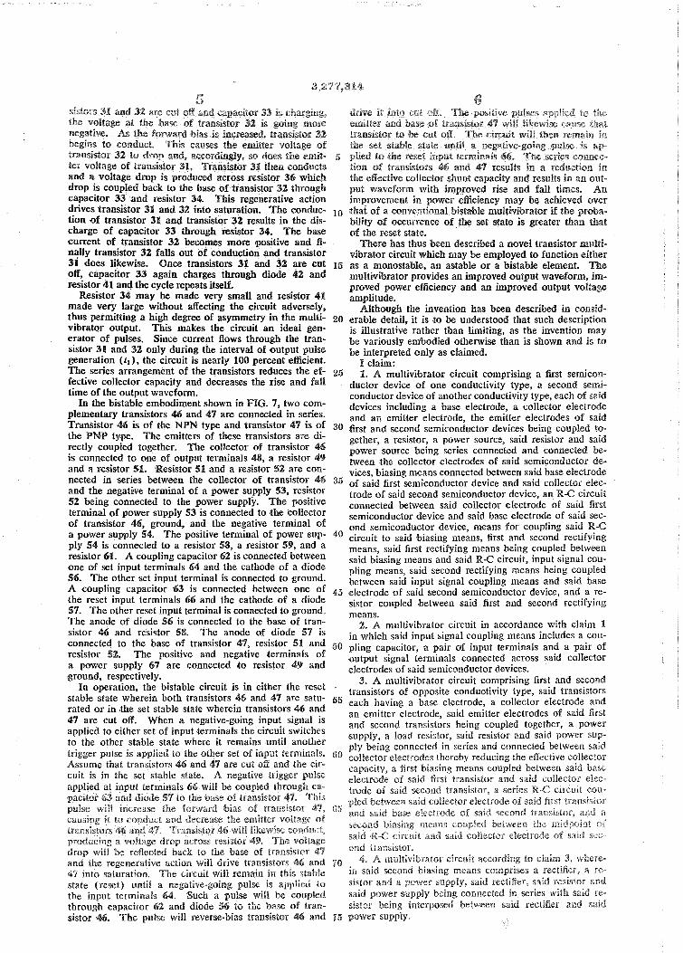
posite conductivity type are coupled in a novel manner to charges through resistor 13 and diode P9. Some of the f ~ r m a muliivibrator. The complementary transistors 110 circuit waveforms are illustrated in FIG. 4. are connected in series with each other and a load resist- FIG. 4 iflustrates the input waveform, the output wave- ace . The load resistance is connected to the collector form, and the waveform ;between the junction of capacitor of the first transistor. The emitter of the first transistor 16 and resistor 23, point a, and ground for ihe circuit de- is connected directly to the emitter of the second transis- picted in FIG. 3. tor. Current flows in both transistors sirnultaneosuly, or 15 In the conventional transistor monostable multivibrator alternatively, both transistors are cut off. This arrange- illustrated in FIG. 1, the output current flows through merit produces a nearly 100 percent efficient multivibrator. resistor & and causes a voltage drop. The total output The series connection of the two complementary transis- voltage is the power supply voltage e2 less the s a t m i o n tors results in a reduction in the effective collector shunt voltage of transistors Q1 and Q2 and the voltage drop capacity and provides a shorter response time. A cir- 20 across resistor R3. In The circuit of FIG. 3, however, cuit embodying the invention may be any one of the three the output voltage is equal to the power supply voltage types of multivibrators, namely, monostable, bistable, or less only the saturation voltages of transistor 11 and 12. astable. A single network coupling the complementary This insures pulse height stability and produces a higher transistors determines whether this circuit is monostable, output voltage for a given power supply. The output bistable or astable. 25 voltage is nearly equal to the power supply voltage. The
The novel features of this invention as well as the in- reduction in the effective collector shunt capacity, by vention itself, both as to its organization and method of series connection of transistors 11 and 12, contributes operation, will be best understood from the following de- to the speed of response of the circuit and allows the scription, when read in connection with the accompanying shortest possible rise and fall times in the output wave- drawings, in which like reference symbols refer to like 30 form. The power consumed in the circuit of FIG. 4 is parts, in which: only the power consumed in the load plus the very mal l
FIG. 1 is a circuit diagram of a conventional semicon- pcnver consumed in the base circuit of transistor 12 dur- ductor monostable multivibrator; ing witching. Stand-by power is zero. Thus, the circuit
FIG. 2 is a circuit diagram of a conventional transistor is substantially 100 percent efticient. This makes the astable multivibrator; 35 circuit ideally suited for those applications where .power
FIG. 3 is a circuit diagram of a monostable multi- consumption is of the utmost Lmportanoe, for example, vibrator embodying this invention; in satellite instmntation.
FIG. 4 illustrates waveforms associated with the cir- The astable embodiment illustrated in FIG. 5 has no cuit of FIG. 3; stable states and provides a free-running oscillator. b
FIG. 5 is a circuit diagram of an astable multivibrator 40 R-C circuit comprising capacitor 33 and resistor 34 is embodying this invention; connected between the base of a PNP transistor 32 and
FIG. 6 illustrates waveforms generated in the circuit the collector of an NPN transistor 31, the capacitor 33 of FIG. 5; and being connected to the collector of the latter transistor.
FIG. 7 is a circuit diagram of a bistable multivibrator The emitters of transistors 31 and 32 are directly coupled. embodying this invention. 4B The collector of transistor 31 is c o ~ e c t e d to capacitor 33,
The embodiment shown in FIG. 3 contains a NPN a resistor 36 and one of output terminals 39. The other transistor 11, the emitter of which is connected to the output terminal is connected to ground. The positive emitter of a PNP transistor 12. The collector of tran- and negative terminals of a power supply 37, generating sistor 11 is connected to one of output terminals 14, a a potential e2, are connected to resistor 36 and ground, load resistor 13, and a capacitor 16. The remaining respectively. The positive and negative terminals of a output terminal is grounded. The positive and negative power supply 38, generating a potential e,, are connected terminals of a power supply 17, generating a potential ea, to the base of transistor 31 and ground, respectively. are connected to resistor 13 and ground, respectively. The The anode of diode 42 is connected lo resistor 34 and negative terminal of a power supply 18, generating a po- capacitor 33 and the cathode is connected to resistor 43.. tential el, is grounded and the positive terminal is con- 55 A power supply 43 is connected between ground and nected to the cathode of a diode 19, a resistor 21, and a resistor 41, the positive terminal of the power supply resist&- 22. The anode of diode 19 is connected to being connected to ground. The negative terminal of capacitor 16 and a resistor 23. Capacitor 16 is con- power supply 38, and the collector of transistor 32 am nected to the collector of transistor I1 and resistor 23 all grounded. is connected to the base of transistor 12. Resistor 21 00 The circuit shown in FIG. 5 is self-skrling and no input is connected between the cathode of a diode 24 and a pulse is required. Transistors 31 and 32 act similarly coupling capacitor 26. Capacitor 26 and diode 24 a x to the transistom in the monostable multivibrator circuit connected in series between one of input terminals 27 of FIG. 3 in that they h t h are saturated or are both cut and the base of transistor 12, The o h r input terminal olf at any given t h e . When transistors 3% and 32 are is grounded. G5 ~"lurated, capacitor 33 discharges through resistor 34,
In operation, both Iwrrsistors l b and 12 are normally Diode 42 is emplayed as a dismnned diode fs isolate cut off becaux no voltage appears between the base of cqacitor 33 sad resistr 34 from resistor 41. TWO of transistor 11 and the base of transistor 12. When a nega- the waveforms generated in the cii-ibuit of FIG. 5 are il- tive pulse appears at the &put terminals 27, it passes userat& in FZG. 6. The p r h d ls during which -lira% through coupiing capacitor 26 and the in-put diode 24 transistors 31. and 32 are saturated is mgulated by the to the base of transistor 12, causing transistor 12 to con- time muslant R34C33 wherein Rs4 is the resistance of re- duct. The voltage el the en?Itter of trznsistor 1% is re- sistor 34 2nd Caa i n the capcitance of capacitor 33. The duced since the emitter of transistor 12 is connected to period fa during which time the transistor 31 and 32 are ?he emitter of transistor 11. This causes trazsistor cut off is mnrralled by the time canstant ( R 4 1 + R ~ ~ f C ~ ~ to begin conducting. Current then flows through resistor 75 wherein is the resistance of resistor 41. When tran-
3,277,814 5 6
sisters 391 and 32 are cot off and f-apmitor 33 is charging, drive It into cut off. The positive pulses applied to tke the volhge at the base d transistor 32. is going more mi t te r and base of hransaar 47 wal likewix cause that negative. As &e fornard bias is i n c ~ d , eansislor 32 transistor to 4% cut off- 7% c ~ b will then remam in begins lo conduct. Tlnis causes the emitter voltage oh the set stable state vndl a ilegatrve-going p u i ~ is zip- transistor 32 to drop and, aaordingly, so does the emit- 5 plied to the reset input terminals &. The series ckonnec- ter voltage of transistor 31. Transistor 31 then conducb tion of transistors 46 and 47 results in a reduction in and a voltage drop is produced across resistor % which the effective coilector shu& capacity and results in an out- drop is coupled back to the base of transistor 32 through put waveform with improved rise and fall times. An capacitor 33 and resistor 34. This regenerative action improvemnt in p e r efficiency may be achieved aver drives transistor 31 and 32 into saturation. The conduc- ahat of a conventional bistA1e mul&&rator if the p&a- tion of transistor 31 and transistor 32 results in the dis- bility d occurrence of the set &ate is greater than &at charge of capacitor 33 through resistor 34. The base of the reset state. current of transistor 32 becomes more positive and fi- There has thus been described a novel transistor multi- nally transistor 32 falls out of conduction and transistor vibrator circuit which may be employed to function either 31 does likewise. Once transistors 31 and 32 are cut 15 as a monostabb, an askble o r a bistable element. m e off, capacitor 33 again charges through diode 42 and muitk8rator provides an improved output wavaform, im- resistor 41 and the cycle repeats itself. proved power efficiency and an improved output voltage
Resistor 34 may be made very small and Mistor 41 made very large without affecting the circuit adversely, Althongh the invention has been described in consid- thus permitting a high degree of asymmetry in the multi- 20 erable detail, it is to be understood that such description vibrator output. This makes the circuit an ideal gen- is illustrative rather than limiting, as the invention may erator of pulses. Since current flows through the tran- b, variously e&odied othenvise than is shown and is to sistor 31 and 32 only during the intervd of output pulse interpreted only as &imed. generation ( t l ) , the circuit is nearly 100 percent efficient. I claim: The series arrangement of the transistors reduces the ef- 25 1, A mnltivibrator circuit comprising a first semicon- fective collector capacity and decreases the rise and fall ductor device of one conductivity type, a second seai- time of the output waveform. conductor device of another conductivity type, each of said
In th ed)odilnent shown in FIG- 7* two devices including a base electrode, a collector electrode plementary transistors 46 and 47 are connected in series- and an emitter elwtmde, the emitter electrodes of said Transistor 46 is of the NPN type and transistor 47 is of 30 first and second devices being coupled io- the PNP ty*. emitten of transistors are di- gether, a resistor, a power source, said resistor and said rectly coupled together. The collector of transistor 45 power being series connected and connected be- is connected t o one of output terminals 48, a resistor 49 tween the collector electrodes of said de- and a resistor 51. 'Resistor 51 and a resistor 52 are con- .ices, biasing means connected between said base elecbode nected in series between the collector of transistor 125 35 of said fint sesemiconductor device and said collector elec- and the aegathe terminal of a power supply 53, resistor trode of said second semiconductor device, an R-C circuit 52 being connected to the power supply. The positive connected &tween said collector electrode of said first terminal of power supply 53 is ~ n ~ ~ e c t e d to the collector semiconductor device and said base electrode of said set- of transistor 46, ground, and the negative terminal of 0.d semiconductor &vice, means lor coupling said R-C a power supply 54. The positive terminal of PwJer SUP- 40 circuit to said biasing means, first and second rectifying ply 54 is connected to a resistor 58, a resistor 59, and a means, said fifst rectifying means being coupled between resistor 61. A coupling capacitor 62 is connected batween said biasing means and said R-c circuit, input signal cou- one of set input terminals 54 and the cathode of a diode pling means, said second rectifying means being coupled 56. The other set input terminal is connected to ground. between said input signal coupling means and said base A coupling capacitor 63 is connected between one of 45 electrode of said second semiconductor device, and a re- the reset input terminals 66 and the cathode of a diode sistor coupled between said first and second rectifying 57. The other reset input terminal is connected to ground. means. The anode of diode 56 is connected to the base of tran- 2. A multivibrator circuit in accordance with claim 1 sistor 46 and resistor 58. The anode of diode 57 is in which said input coupling includes a cou- connected to the base of transistor 47, resistor 51 and 50 pling capacitor, a pair af input terminals and a pair of resig~r 52. The positive and negative output signal t e ~ i n a l s connected across said collector a power supply 67 are Connected 49 and electrodes of said semiconductor devices. ground, respectively. 3. A multivibrator circuit comprising first and second
In operation, the bistable circuit is in either the reset transistors of opposite type, said transistors stable state wherein both 46 and 47 are satu- 55 each having a base electrode, a collector electrode and rated or in the set stable state wherein transistors 46 and an emitter electrode, said emitter electrodes of said firsf 47 are cut off. m e n 2 negative-going input signal is and transistors being coupled together, a power applied to either set of input terminals the circuit switches supply, a load resistor, said resistor and said power sup- to the other stable state where it remains until another ply being connected in series and connected between said trigger pulse is applied to the other set of input terminals. 60 coffeCtor electrodes thereby reducing the efiecrive coIiector Assume that transistors 46 and 4'7 are cut off and the cir- a first biasing means coupled between said b a s cuit is in the set stable state. A negative trigger pulse of said first transistor and said elec- applied at input terminals 66 will be coupled through ca- trode d said second transistor, a series R-C circuit cou- pacitor a and diode to Ihe bacx o.f lransisaor 47s pled said collector electrode of said first transistor pulse will increax the fornard bias of transistor 47% 05 and said base said and a causing it to conduct and decrease the emilier voltage of transirtoi3 06 and l(l. Iran,isior will i,Xewire
second biaiiiig means coupled betaren the elnidpoini of a drop The said R E circuit and said collector electrode of sad irs-
drop will bedected back to the base of transistor 47 rind transistor. and the will drive .)6 and 1. A multivibrator circuit according to claim 3, where- 47 inlo saturation, 'rhe circuit will remain in :his $table in said second biasing means comprises a rectilier, a re-
state (reset) a negatjve-goiag pulse is appiicd to sistor an4 a power supply, 5.4 rectifier, said resistor and the input terminals 64. Such a pulse will be coupbd said power supply being connected in series with said re- through 62 and diode % to ;he b a s of :ran- dsrnr being i*terpo&- Itetww-en said rectikr and said sistor &. The pulse will reverse-bias ~a~ansistor 4-6 and T g p w e r supply.

3,877,814
7 8 5. A bietabk mul&ibl.ator cornpkhg Basl and second kaor e I a d s of saki ma'md W~~SOI ; and a msst~r
tmnsktslors each having base, emilkr a d m w o r eW- coupkid be-n said C O M X ~ O ~ ekMg. of said hi: tr&s, mid miter e k f r d r i 01 said masistow bekg tmsisfisr md base- e W & of said ~ ~ n d LrarcskW~ c011pId Poge&e& a Brst d s l o r d a can- m c t d in series & w e n said cdkctor mid g first and second transistors, a set ioput, a h t diode and
said set inwt and 3,Wf@39 5/1963 Walls ----,--------- 3 0 7 4 8 . 5 said first transistor, a @set inpntt, a sec- 3,103,595 99/1963 ------------- 3W-485 second capacitor wupM hwen said 3,113,217 12/1963 et al. ,------- 307483
input and said base eIectrode oi said second 10 3,131,362 4/19M mTSGh ------------ 307-48.9. Gst5r3 a pair of resisbrs serially connected between the 3D521 t211s5 whter ,,----,,---- 307-485 junction of said first diode and said first ~gac i tor and
Primapy E m i m r . tor, dirst biasing means wupled to said pair o
and said base electrode sf said first IN, R&tmt Emincr.