d computer-aided circuit analysis - pearson
TRANSCRIPT

APPENDIX
D Computer-Aided CircuitAnalysisOne of the earliest circuit-analysis programs, known as SPICE (an acronym forSimulation Program with Integrated Circuit Emphasis), was developed by theElectronics Research Laboratory at the University of California in the early 1970s.Several commercial versions of SPICE have since been produced that include a widevariety of useful extensions to the original program.
In this appendix, we show how to use OrCAD 10.5, a suite of programs byCadence Design Systems, to analyze most of the types of circuits discussed inUsing OrCAD 10.5, you can
check your answers to manyof the problems in this book.
this book. This suite of programs is a very sophisticated and powerful tool forelectronic-circuit designers.
D.1 ANALYSIS OF DC CIRCUITS
Menu selections are printed inbold with slashes separatingsuccessive selections. Thus,Help/Learning Capture CISindicates that we should placethe cursor on Help (at thetop of the Capture window),click the left mouse button topull down a menu, move thecursor to Learning CaptureCIS, and click the left mousebutton.
First, you should use the OrCAD 10.5 Demo disk included with this book to installthe software on your computer.
Then, use the start menu on your computer to start Capture CIS Demo, whichis located in the OrCAD 10.5 Demo program group. (If you wish to learn moreabout the software after finishing this appendix, you can use the Help/LearningCapture CIS command to bring up the Capture tutorial. Then, you can work yourway through the lessons to become familiar with additional features of Capture.)
Using Capture/PSpice to Solve DC Circuits
Next, we illustrate how to solve dc circuits using Capture and PSpice. As a firstexample, we will solve the circuit shown in Figure 2.7(a) on page 56. You will learnbest if you follow along on your computer.This font (Courier)
is used to indicatematerial that youshould type infrom your keyboard.
First, create your own project folder named Student OrCAD Projects in aconvenient location on your hard drive. Then, return to the Capture window and usethe File/New/Project command to bring up the window shown in Figure D.1(a). Typein the name of the project: Figure 2 7a. Then, check the Analog or Mixed A/Doption, click on Browse . . . , navigate to your project folder as shown in Figure D.1(a),and left-click on OK. This brings up the window shown in Figure D.1(b). Left-click on Create a blank project, then on OK. This produces the screen shown inFigure D.2, which contains several windows. We will draw the circuit in the windowtitled SCHEMATIC1: PAGE 1.
Placing Parts
Next, use the Place/Part command to bring up the window shown in Figure D.3.The first time you use this program, you will need to add libraries from which parts
880
Electrical Engineering, Fourth Edition, by Allan R. Hambley. ISBN-13: 978-0-13-198922-1. © 2008 Pearson Education, Inc., Upper Saddle River, NJ. All rights reserved.
This material is protected by Copyright and written permission should be obtained from the publisher prior to any prohibited reproduction, storage in a retrieval system, or transmission in any form or by any means, electronic, mechanical, photocopying, recording, or likewise.
For information regarding permission(s), write to: Rights and Permissions Department, Pearson Education, Inc., Upper Saddle River, NJ 07458.

Section D.1 Analysis of DC Circuits 881
Click the Browse button andnavigate to your project folder
(a)
(b)
Type theproject
name here
Select thisoption
Select thisoption
Figure D.1 We use these windows to create a new project.
are selected. To accomplish this, click on Add Library . . . as indicated in FigureD.3. Then, in the window that opens, select all of the libraries shown, and click onOpen. Type the letter R in the Part window and left-click on OK. At this point, youcan move the cursor around on the SCHEMATIC window and place a resistor eachtime you click the left mouse button. The orientation of the resistor can be rotatedby pressing the ‘‘control’’ and ‘‘r’’ keys simultaneously. Place four resistors as shownin Figure D.4. Then, click the right mouse button and select End Mode from thepop-up menu. Next, place the voltage source (its name is VDC) by again using thePlace/Part command.
Electrical Engineering, Fourth Edition, by Allan R. Hambley. ISBN-13: 978-0-13-198922-1. © 2008 Pearson Education, Inc., Upper Saddle River, NJ. All rights reserved.
This material is protected by Copyright and written permission should be obtained from the publisher prior to any prohibited reproduction, storage in a retrieval system, or transmission in any form or by any means, electronic, mechanical, photocopying, recording, or likewise.
For information regarding permission(s), write to: Rights and Permissions Department, Pearson Education, Inc., Upper Saddle River, NJ 07458.

882 Appendix D Computer-Aided Circuit Analysis
Figure D.2 We use these windows to draw the circuit.
All of this might take a few tries. The steps (and some helpful tips) are asfollows:
1. Use the Place/Part command to bring up the window from which parts can beselected. For now, we only need R for resistors and VDC for dc voltage sources.
2. After selecting the desired part, click on OK. If necessary, depress the ‘‘control’’and ‘‘r’’ keys simultaneously to rotate the part to the desired orientation. Then,move the cursor to the desired location and left-click to place a part. After allthe parts of a given type are placed, click the right mouse button and select EndMode on the pop-up menu.
3. If you accidentally get an unneeded part, you can eliminate it after you leavethe place-part mode. Select the unwanted part by placing the cursor on it andclicking the left mouse button. Then, press the delete key.
4. If a part has the wrong name (such as R7 instead of R4), change it after youleave the place-part mode. Double left-click on the name and type in the correctname. (However, two or more parts must not have the same name when we dothe PSpice analysis.)
Electrical Engineering, Fourth Edition, by Allan R. Hambley. ISBN-13: 978-0-13-198922-1. © 2008 Pearson Education, Inc., Upper Saddle River, NJ. All rights reserved.
This material is protected by Copyright and written permission should be obtained from the publisher prior to any prohibited reproduction, storage in a retrieval system, or transmission in any form or by any means, electronic, mechanical, photocopying, recording, or likewise.
For information regarding permission(s), write to: Rights and Permissions Department, Pearson Education, Inc., Upper Saddle River, NJ 07458.
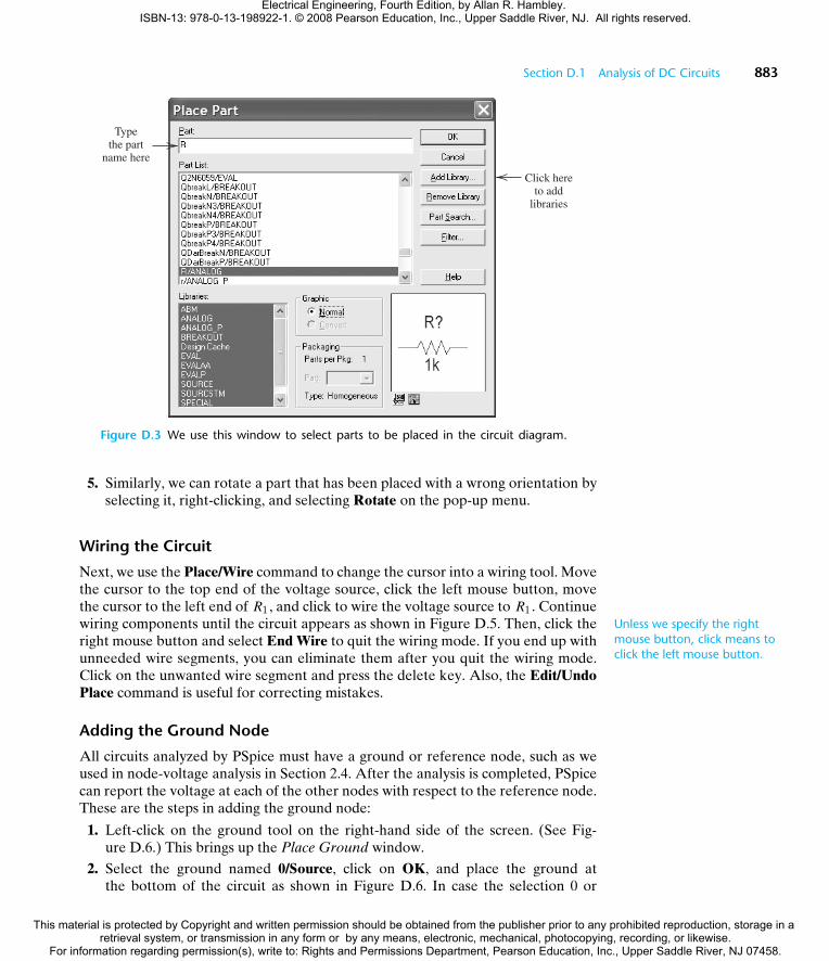
Section D.1 Analysis of DC Circuits 883
Typethe part
name here
Click hereto add
libraries
Figure D.3 We use this window to select parts to be placed in the circuit diagram.
5. Similarly, we can rotate a part that has been placed with a wrong orientation byselecting it, right-clicking, and selecting Rotate on the pop-up menu.
Wiring the Circuit
Next, we use the Place/Wire command to change the cursor into a wiring tool. Movethe cursor to the top end of the voltage source, click the left mouse button, movethe cursor to the left end of R1 , and click to wire the voltage source to R1 . Continuewiring components until the circuit appears as shown in Figure D.5. Then, click the Unless we specify the right
mouse button, click means toclick the left mouse button.
right mouse button and select End Wire to quit the wiring mode. If you end up withunneeded wire segments, you can eliminate them after you quit the wiring mode.Click on the unwanted wire segment and press the delete key. Also, the Edit/UndoPlace command is useful for correcting mistakes.
Adding the Ground Node
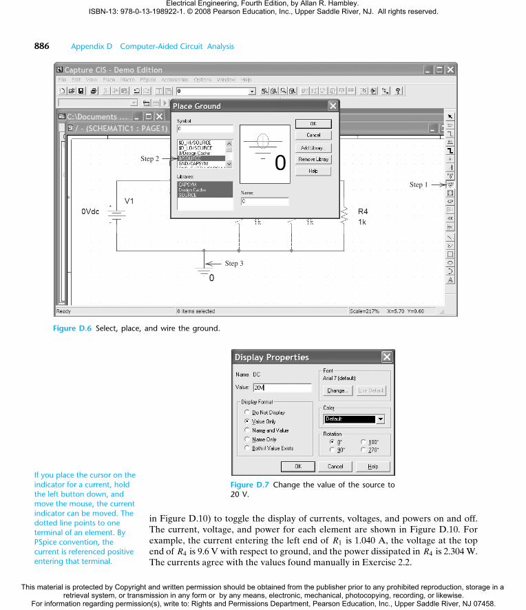
All circuits analyzed by PSpice must have a ground or reference node, such as weused in node-voltage analysis in Section 2.4. After the analysis is completed, PSpicecan report the voltage at each of the other nodes with respect to the reference node.These are the steps in adding the ground node:
1. Left-click on the ground tool on the right-hand side of the screen. (See Fig-ure D.6.) This brings up the Place Ground window.
2. Select the ground named 0/Source, click on OK, and place the ground atthe bottom of the circuit as shown in Figure D.6. In case the selection 0 or
Electrical Engineering, Fourth Edition, by Allan R. Hambley. ISBN-13: 978-0-13-198922-1. © 2008 Pearson Education, Inc., Upper Saddle River, NJ. All rights reserved.
This material is protected by Copyright and written permission should be obtained from the publisher prior to any prohibited reproduction, storage in a retrieval system, or transmission in any form or by any means, electronic, mechanical, photocopying, recording, or likewise.
For information regarding permission(s), write to: Rights and Permissions Department, Pearson Education, Inc., Upper Saddle River, NJ 07458.

884 Appendix D Computer-Aided Circuit Analysis
Figure D.4 Parts have been placed.
0/Source does not appear on the menu, click Add Library: : : , select the filesource.olb from the PSpice folder, and click on Open. The complete path tothis file is
c:\OrCAD\OrCAD 10.5 Demo\tools\capture\library\pspice\source
After placing the ground symbol, right-click and select End Mode.
3. Use the Place/Wire command to change the cursor to a wiring tool and wire theground to the circuit as shown in Figure D.6.
Changing Component Values
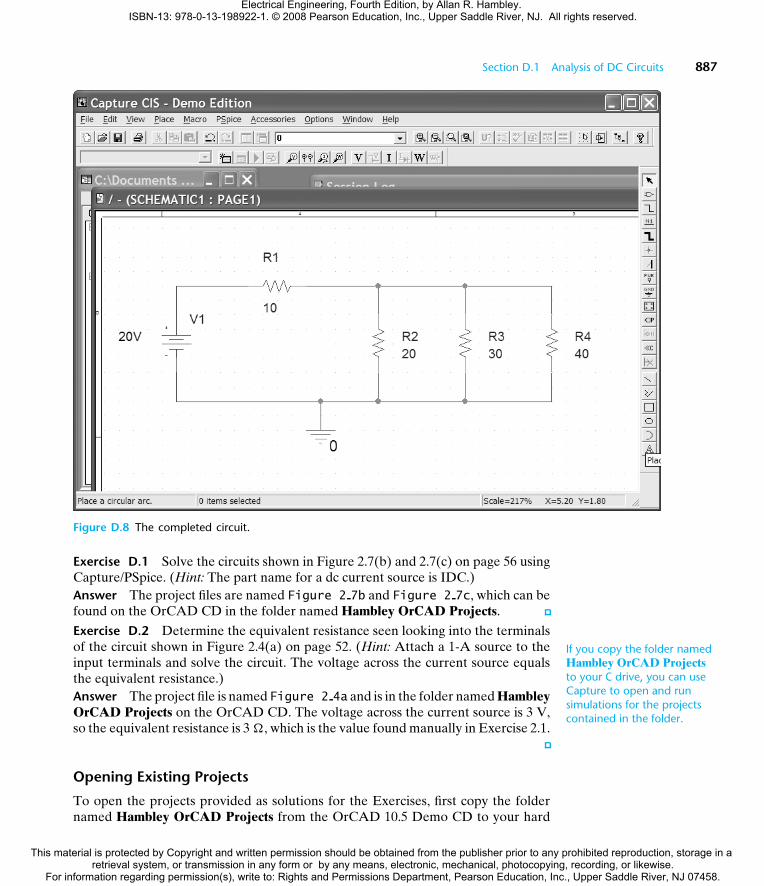
Next, we change the default component values to those shown in Figure 2.7(a) onpage 56. Double left-click on 0Vdc next to the voltage source to bring up the windowshown in Figure D.7. Enter 20V as the new value, and then click on OK to closethe window. In a similar fashion, change the values of the resistances so that R1 is10, R2 is 20, R3 is 30, and R4 is 40. (If you want to, you can change the names ofthe elements as well. For example, we could change V1 to Vs to better match the
Electrical Engineering, Fourth Edition, by Allan R. Hambley. ISBN-13: 978-0-13-198922-1. © 2008 Pearson Education, Inc., Upper Saddle River, NJ. All rights reserved.
This material is protected by Copyright and written permission should be obtained from the publisher prior to any prohibited reproduction, storage in a retrieval system, or transmission in any form or by any means, electronic, mechanical, photocopying, recording, or likewise.
For information regarding permission(s), write to: Rights and Permissions Department, Pearson Education, Inc., Upper Saddle River, NJ 07458.

Section D.1 Analysis of DC Circuits 885
Figure D.5 Use the Place/Wire command to bring up the wiring tool and wire the circuit.
element names shown in Figure 2.7.) Now, the circuit should appear as shown inFigure D.8.
Setting Up a New Simulation Profile
Simulation profiles tell PSpice what type of analysis is desired. Next, use the PSpice/New Simulation Profile command to bring up the window shown in Figure D.9(a).Type in DC Solution as the name of the simulation profile, make sure that theInherit From window contains the word none, and left-click on Create. This bringsup the window shown in Figure D.9(b). Use the pull-down menu and select BiasPoint as the analysis type. Then, click on OK. The simulation profile we have createdinstructs PSpice to compute the voltages at the circuit nodes, the current througheach element, and the power dissipated in each element.
Running the PSpice Simulation
Next, use the PSpice/Run command to run the simulation. Close the SCHEMATIC1-DC Solution window that appears. Next, click on the V, I, and W icons (shown
Electrical Engineering, Fourth Edition, by Allan R. Hambley. ISBN-13: 978-0-13-198922-1. © 2008 Pearson Education, Inc., Upper Saddle River, NJ. All rights reserved.
This material is protected by Copyright and written permission should be obtained from the publisher prior to any prohibited reproduction, storage in a retrieval system, or transmission in any form or by any means, electronic, mechanical, photocopying, recording, or likewise.
For information regarding permission(s), write to: Rights and Permissions Department, Pearson Education, Inc., Upper Saddle River, NJ 07458.
886 Appendix D Computer-Aided Circuit Analysis
Step 2
Step 1
Step 3
Figure D.6 Select, place, and wire the ground.
Figure D.7 Change the value of the source to20 V.
in Figure D.10) to toggle the display of currents, voltages, and powers on and off.
If you place the cursor on theindicator for a current, holdthe left button down, andmove the mouse, the currentindicator can be moved. Thedotted line points to oneterminal of an element. ByPSpice convention, thecurrent is referenced positiveentering that terminal.
The current, voltage, and power for each element are shown in Figure D.10. Forexample, the current entering the left end of R1 is 1.040 A, the voltage at the topend of R4 is 9.6 V with respect to ground, and the power dissipated in R4 is 2.304 W.The currents agree with the values found manually in Exercise 2.2.
Electrical Engineering, Fourth Edition, by Allan R. Hambley. ISBN-13: 978-0-13-198922-1. © 2008 Pearson Education, Inc., Upper Saddle River, NJ. All rights reserved.
This material is protected by Copyright and written permission should be obtained from the publisher prior to any prohibited reproduction, storage in a retrieval system, or transmission in any form or by any means, electronic, mechanical, photocopying, recording, or likewise.
For information regarding permission(s), write to: Rights and Permissions Department, Pearson Education, Inc., Upper Saddle River, NJ 07458.
Section D.1 Analysis of DC Circuits 887
Figure D.8 The completed circuit.
Exercise D.1 Solve the circuits shown in Figure 2.7(b) and 2.7(c) on page 56 usingCapture/PSpice. (Hint: The part name for a dc current source is IDC.)Answer The project files are named Figure 2 7b and Figure 2 7c, which can befound on the OrCAD CD in the folder named Hambley OrCAD Projects.
Exercise D.2 Determine the equivalent resistance seen looking into the terminalsof the circuit shown in Figure 2.4(a) on page 52. (Hint: Attach a 1-A source to theinput terminals and solve the circuit. The voltage across the current source equalsthe equivalent resistance.)Answer The project file is named Figure 2 4a and is in the folder named Hambley
If you copy the folder namedHambley OrCAD Projectsto your C drive, you can useCapture to open and runsimulations for the projectscontained in the folder.OrCAD Projects on the OrCAD CD. The voltage across the current source is 3 V,
so the equivalent resistance is 3 �, which is the value found manually in Exercise 2.1.
Opening Existing Projects
To open the projects provided as solutions for the Exercises, first copy the foldernamed Hambley OrCAD Projects from the OrCAD 10.5 Demo CD to your hard
Electrical Engineering, Fourth Edition, by Allan R. Hambley. ISBN-13: 978-0-13-198922-1. © 2008 Pearson Education, Inc., Upper Saddle River, NJ. All rights reserved.
This material is protected by Copyright and written permission should be obtained from the publisher prior to any prohibited reproduction, storage in a retrieval system, or transmission in any form or by any means, electronic, mechanical, photocopying, recording, or likewise.
For information regarding permission(s), write to: Rights and Permissions Department, Pearson Education, Inc., Upper Saddle River, NJ 07458.

888 Appendix D Computer-Aided Circuit Analysis
(a)
(b)
Figure D.9 Windows used to set up the simulation profile.
drive. Then, to open the solution for Exercise D.2, start Capture CIS, use theFile/Open/Project . . . command, navigate to the desired project, which in this caseis named Figure 2 4a, and double-click on it. Then, navigate to Page 1 of Schematic1 as shown in Figure D.11 and double-click on it to bring up the window containingthe circuit diagram.
Controlled Sources
Capture and PSpice can also simulate circuits that contain controlled sources. Exceptfor setting the gain parameters of the controlled sources, the steps are very similarto those we used previously. The part names of the controlled sources are as follows:
E voltage-controlled voltage sourceG voltage-controlled current sourceH current-controlled voltage sourceF current-controlled current source
Electrical Engineering, Fourth Edition, by Allan R. Hambley. ISBN-13: 978-0-13-198922-1. © 2008 Pearson Education, Inc., Upper Saddle River, NJ. All rights reserved.
This material is protected by Copyright and written permission should be obtained from the publisher prior to any prohibited reproduction, storage in a retrieval system, or transmission in any form or by any means, electronic, mechanical, photocopying, recording, or likewise.
For information regarding permission(s), write to: Rights and Permissions Department, Pearson Education, Inc., Upper Saddle River, NJ 07458.

Section D.1 Analysis of DC Circuits 889
Voltage, current, and power icons.
Figure D.10 After running PSpice, the voltages, currents, and powers can be displayed on the schematic.
Figure D.12 shows the appearance of the various controlled sources in Capture. Asthe symbols are oriented in Figure D.12, the controlling variable should be wired tothe terminals on the left-hand side, and the source terminals are on the right-handside. (Of course, if we flip or rotate the symbol, either set of terminals may be at thetop, bottom, left, or right.)
As an example, we solve for ix in the circuit shown in Figure 2.30(a) on page 75which contains a current-controlled current source. First, we place the elements (thename of the controlled source is F), place the ground, and wire the circuit, as we didearlier in this appendix. The Capture screen is shown in Figure D.13. Notice that wehave flipped and rotated the controlled source, so that the source terminals are onthe left-hand side. Then, the controlling variable ix is wired to the input terminals.Compare the screen display with the original circuit shown in Figure 2.30(a).
To set the gain parameter of the controlled source, we double left-click on thecontrolled source, bringing up the window shown in Figure D.14. Here, we enterthe gain as 2, click on Apply, and close the window. Then, we set up the simulationprofile to perform a Bias Point analysis, run PSpice, and observe the results on theCapture screen. As in the manual analysis that we did for Exercise 2.13, we obtainix D 0:5 A. This project is stored in the file named Figure 2 30a.
Electrical Engineering, Fourth Edition, by Allan R. Hambley. ISBN-13: 978-0-13-198922-1. © 2008 Pearson Education, Inc., Upper Saddle River, NJ. All rights reserved.
This material is protected by Copyright and written permission should be obtained from the publisher prior to any prohibited reproduction, storage in a retrieval system, or transmission in any form or by any means, electronic, mechanical, photocopying, recording, or likewise.
For information regarding permission(s), write to: Rights and Permissions Department, Pearson Education, Inc., Upper Saddle River, NJ 07458.

890 Appendix D Computer-Aided Circuit Analysis
Figure D.11 Double-click on PAGE1 to open the schematic (if it is not open already).
Voltage-controlledvoltage source
Voltage-controlledcurrent source
Current-controlledvoltage source
Current-controlledcurrent source
Figure D.12 Controlled sources.
Electrical Engineering, Fourth Edition, by Allan R. Hambley. ISBN-13: 978-0-13-198922-1. © 2008 Pearson Education, Inc., Upper Saddle River, NJ. All rights reserved.
This material is protected by Copyright and written permission should be obtained from the publisher prior to any prohibited reproduction, storage in a retrieval system, or transmission in any form or by any means, electronic, mechanical, photocopying, recording, or likewise.
For information regarding permission(s), write to: Rights and Permissions Department, Pearson Education, Inc., Upper Saddle River, NJ 07458.

Section D.1 Analysis of DC Circuits 891
ix
ix
Figure D.13 The circuit of Figure 2.30(a) on page 75 drawn with Capture.
Click to show or hidecurrent-controlled
current sources
Enter gain value here
Figure D.14 This window is used to set the gain of the controlled source.
Electrical Engineering, Fourth Edition, by Allan R. Hambley. ISBN-13: 978-0-13-198922-1. © 2008 Pearson Education, Inc., Upper Saddle River, NJ. All rights reserved.
This material is protected by Copyright and written permission should be obtained from the publisher prior to any prohibited reproduction, storage in a retrieval system, or transmission in any form or by any means, electronic, mechanical, photocopying, recording, or likewise.
For information regarding permission(s), write to: Rights and Permissions Department, Pearson Education, Inc., Upper Saddle River, NJ 07458.

892 Appendix D Computer-Aided Circuit Analysis
Exercise D.3 Solve the circuit shown in Figure 2.30(b) on page 75 using Capture/PSpice. (Hint: The part name for a current-controlled voltage source is H, and thename for a constant current source is IDC.)Answer The project file is Figure 2 30b, which can be found on the OrCAD CDin the folder named Hambley OrCAD Projects. As in the manual analysis, we findiy D 2:31 A.
D.2 TRANSIENT ANALYSIS
Next, we show how to perform transient analysis of RLC circuits, as we did bytraditional analysis in Chapter 4. In transient analysis, we often have switches thatopen or close at t D 0. We draw the circuit with the switches in their final positionsand specify the initial voltages for capacitors and initial currents for inductors. Then,PSpice analyzes the circuit for t > 0.
As an example, we use PSpice to analyze the circuit of Figure 4.7 on page 164.First, we set up a new project named Figure 4 7, place the elements, and wire theThe element names for
inductors and capacitors are Land C, respectively.
circuit. (Don’t forget to include a ground.) Because the switch is closing, it is a shortcircuit for t > 0 and appears as a wire in Capture. The resulting Capture window isshown in Figure D.15.
Next, we specify the initial (i.e., immediately after t D 0/ current flowing in theinductor. In this circuit, the initial current is zero. Double left-click on the inductorto bring up the window shown in Figure D.16. Enter 0 for the initial condition (IC)as shown. Then, click on Apply and close the window.
Setting Up a Simulation Profile for Transient Analysis
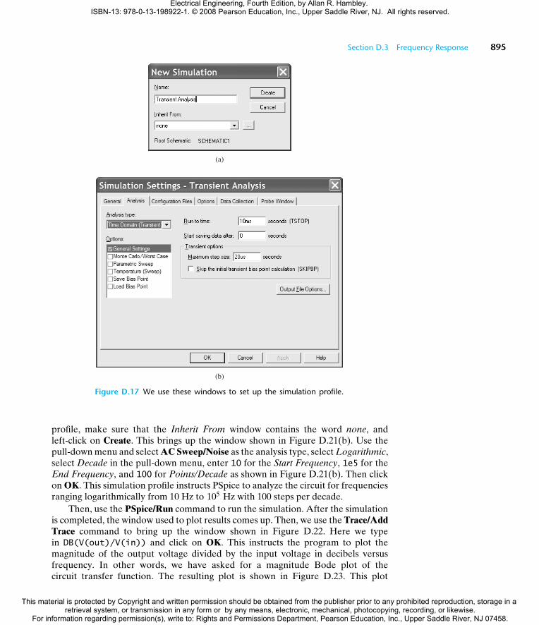
Next, use the PSpice/New Simulation Profile command to bring up the windowshown in Figure D.17(a). Type in Transient Analysis as the name of thesimulation profile, make sure that the Inherit From window contains the word none,and left-click on Create. This brings up the window shown in Figure D.17(b). Usethe pull-down menu, and select Time Domain (Transient) as the analysis type.
PSpice performs transient analysis by using the initial values of the voltages andcurrents to compute the circuit responses a short time later. Then, these values areused to compute the responses at the next time point. PSpice adjusts the time stepbetween computed values as the solution proceeds. Higher accuracy is providedby a small step size, but it results in long execution times. Therefore, PSpice usesa small time step if the response is changing rapidly, and a larger step if theresponse is changing more slowly. Also, when we plot the results, a small timestep results in a smooth curve. In the Simulation Settings window, we can specifythe maximum time step to be used as well as how long we want the simulation toproceed.
We must select appropriate parameters for the time-domain analysis for the cir-cuit at hand. In this circuit, we know that the current approaches its final value witha time constant of L=R D 2 ms. A smooth plot can be obtained by selecting the max-imum step to be about 1 percent of the time constant. Thus, we select the Maximum
Electrical Engineering, Fourth Edition, by Allan R. Hambley. ISBN-13: 978-0-13-198922-1. © 2008 Pearson Education, Inc., Upper Saddle River, NJ. All rights reserved.
This material is protected by Copyright and written permission should be obtained from the publisher prior to any prohibited reproduction, storage in a retrieval system, or transmission in any form or by any means, electronic, mechanical, photocopying, recording, or likewise.
For information regarding permission(s), write to: Rights and Permissions Department, Pearson Education, Inc., Upper Saddle River, NJ 07458.

Section D.2 Transient Analysis 893
Figure D.15 The circuit of Figure 4.7 on page 164 drawn with Capture.
step size to be 20 ¼s. (In Capture, the letter u represents the Greek letter ¼ in nu-merical values.) Furthermore, we know that the response approaches its final valuewithin a negligible error in about five time constants. Therefore, we select the Run totime value as 10 ms. (This instructs PSpice to stop the analysis when t reaches 10 ms.)
In more complex circuits for which the results are not known in advance, wemay need to play around with these parameters (Run to time and Maximum stepsize). Usually, engineers are designing circuits for which they know the approximateresponse in advance, and selecting the analysis parameters is not a major problem.
Running the Simulation and Viewing the Results
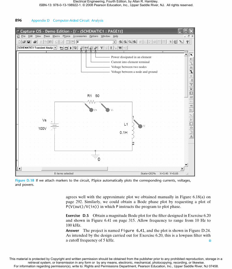
Next, we attach markers to the circuit to specify which currents and voltages wewish to observe. Markers are available to observe the voltage at any node (withrespect to ground), the voltage between any two nodes, the power dissipated in anyelement, and the current entering an element terminal. The icons needed to bringup these markers are shown in Figure D.18. We attach a marker to observe thevoltage across the resistor and a marker to observe the voltage at the top node ofthe inductor, as shown in the figure.
Electrical Engineering, Fourth Edition, by Allan R. Hambley. ISBN-13: 978-0-13-198922-1. © 2008 Pearson Education, Inc., Upper Saddle River, NJ. All rights reserved.
This material is protected by Copyright and written permission should be obtained from the publisher prior to any prohibited reproduction, storage in a retrieval system, or transmission in any form or by any means, electronic, mechanical, photocopying, recording, or likewise.
For information regarding permission(s), write to: Rights and Permissions Department, Pearson Education, Inc., Upper Saddle River, NJ 07458.

894 Appendix D Computer-Aided Circuit Analysis
Click here toshow or hide the
inductors
Enter initial current here
Figure D.16 We use this window to specify the initial current in the inductor.
Next, use the PSpice/Run command to run the simulation. This brings up awindow that displays the voltages. The voltage plots are shown in Figure D.19.Notice that the plot for the voltage across the inductor agrees with the plot shownin Figure 4.8(b) on page 165.
Exercise D.4 Use PSpice to observe the voltage across the capacitor in the circuitshown in Figure 4.21 on page 178 for R D 100 �. Repeat for R D 200 and 300 �.Answer The project is named Figure 4 21 and is stored on the OrCAD CD. Theplots are similar to those shown in Figure 4.26 on page 183.
D.3 FREQUENCY RESPONSE
Another type of analysis that PSpice can perform is to determine and plot thefrequency response of a circuit as we did by traditional analysis in Chapter 6. As anexample, we analyze the circuit shown in Figure 6.17 on page 292.
First, we set up a new project named Figure 6 17, place the elements (thename of the ac voltage source is VAC), and wire the circuit. We included a groundat the bottom of the circuit. Next, we name the input and output nodes of the circuit.To do this, we use the Place/Net Alias command to bring up the window shown inFigure D.20(a). Next, we type in as the name of the input node, click on OK, placethe name field on the wire connected to the top of the source, and left-click. Then,we right-click and select End Mode. Similarly, we name the output node out. Theresulting Capture window is shown in Figure D.20(b).
Setting Up a Simulation Profile for Frequency Response Analysis
Next, use the PSpice/New Simulation Profile command to bring up the windowshown in Figure D.21(a). Type in Frequency Sweep as the name of the simulation
Electrical Engineering, Fourth Edition, by Allan R. Hambley. ISBN-13: 978-0-13-198922-1. © 2008 Pearson Education, Inc., Upper Saddle River, NJ. All rights reserved.
This material is protected by Copyright and written permission should be obtained from the publisher prior to any prohibited reproduction, storage in a retrieval system, or transmission in any form or by any means, electronic, mechanical, photocopying, recording, or likewise.
For information regarding permission(s), write to: Rights and Permissions Department, Pearson Education, Inc., Upper Saddle River, NJ 07458.
Section D.3 Frequency Response 895
(a)
(b)
Figure D.17 We use these windows to set up the simulation profile.
profile, make sure that the Inherit From window contains the word none, andleft-click on Create. This brings up the window shown in Figure D.21(b). Use thepull-down menu and select AC Sweep/Noise as the analysis type, select Logarithmic,select Decade in the pull-down menu, enter 10 for the Start Frequency, 1e5 for theEnd Frequency, and 100 for Points/Decade as shown in Figure D.21(b). Then clickon OK. This simulation profile instructs PSpice to analyze the circuit for frequenciesranging logarithmically from 10 Hz to 105 Hz with 100 steps per decade.
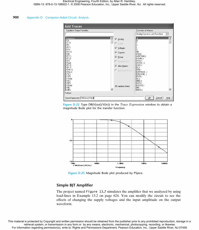
Then, use the PSpice/Run command to run the simulation. After the simulationis completed, the window used to plot results comes up. Then, we use the Trace/AddTrace command to bring up the window shown in Figure D.22. Here we typein DB(V(out)/V(in)) and click on OK. This instructs the program to plot themagnitude of the output voltage divided by the input voltage in decibels versusfrequency. In other words, we have asked for a magnitude Bode plot of thecircuit transfer function. The resulting plot is shown in Figure D.23. This plot
Electrical Engineering, Fourth Edition, by Allan R. Hambley. ISBN-13: 978-0-13-198922-1. © 2008 Pearson Education, Inc., Upper Saddle River, NJ. All rights reserved.
This material is protected by Copyright and written permission should be obtained from the publisher prior to any prohibited reproduction, storage in a retrieval system, or transmission in any form or by any means, electronic, mechanical, photocopying, recording, or likewise.
For information regarding permission(s), write to: Rights and Permissions Department, Pearson Education, Inc., Upper Saddle River, NJ 07458.
896 Appendix D Computer-Aided Circuit Analysis
Power dissipated in an element
Current into element terminal
Voltage between two nodes
Voltage between a node and ground
Figure D.18 If we attach markers to the circuit, PSpice automatically plots the corresponding currents, voltages,and powers.
agrees well with the approximate plot we obtained manually in Figure 6.18(a) onpage 292. Similarly, we could obtain a Bode phase plot by requesting a plot ofP(V(out)/V(in)) in which P instructs the program to plot phase.
Exercise D.5 Obtain a magnitude Bode plot for the filter designed in Exercise 6.20and shown in Figure 6.41 on page 315. Allow frequency to range from 10 Hz to100 kHz.Answer The project is named Figure 6 41, and the plot is shown in Figure D.24.As intended by the design carried out for Exercise 6.20, this is a lowpass filter witha cutoff frequency of 5 kHz.
Electrical Engineering, Fourth Edition, by Allan R. Hambley. ISBN-13: 978-0-13-198922-1. © 2008 Pearson Education, Inc., Upper Saddle River, NJ. All rights reserved.
This material is protected by Copyright and written permission should be obtained from the publisher prior to any prohibited reproduction, storage in a retrieval system, or transmission in any form or by any means, electronic, mechanical, photocopying, recording, or likewise.
For information regarding permission(s), write to: Rights and Permissions Department, Pearson Education, Inc., Upper Saddle River, NJ 07458.

Section D.4 Other Examples 897
Figure D.19 Plots of the voltage across the resistor and across the induc-tor versus time.
D.4 OTHER EXAMPLES
Several other interesting examples showing analysis of circuits from this book areincluded in the folder named Hambley OrCAD Projects on the OrCAD CD. Eachproject file is named for a corresponding figure in the book.
Half-Wave Rectifier
The project named Figure 10 24 is a simulation of a half-wave rectifier circuit.The model for a real diode (the 1N4002) is used, and the input is a 1-kHz 10-V-peaksinewave. The half-wave rectified signal is applied to a 100-� load.
Peak Rectifier
The project named Figure 10 26 is a simulation of a peak rectifier. After thesimulation runs, the diode and load current are plotted. Because the initial volt-age on the capacitor is zero, the first current pulse through the diode is verylarge. After that, the waveforms are similar to those shown in Figure 10.26 onpage 487.
Clipper Circuit
The project named Figure 10 29 simulates the clipper circuit shown in Figure 10.29on page 491 except that the voltage sources have been adjusted to account for theforward drop of a real diode. This project has two simulation profiles, one fordisplaying the waveforms as in Figure 10.29(b) and the other for displaying thetransfer characteristic as in Figure 10.29(c). (You can select the active simulationprofile by clicking on it in the project window shown in Figure D.25 and then byusing the PSpice/Make Active command in the main window.)
Electrical Engineering, Fourth Edition, by Allan R. Hambley. ISBN-13: 978-0-13-198922-1. © 2008 Pearson Education, Inc., Upper Saddle River, NJ. All rights reserved.
This material is protected by Copyright and written permission should be obtained from the publisher prior to any prohibited reproduction, storage in a retrieval system, or transmission in any form or by any means, electronic, mechanical, photocopying, recording, or likewise.
For information regarding permission(s), write to: Rights and Permissions Department, Pearson Education, Inc., Upper Saddle River, NJ 07458.

898 Appendix D Computer-Aided Circuit Analysis
(a)
(b)
Figure D.20 We use the Place Net Alias window to name nodes in a circuit.
MOSFET Curves
The project named Figure 12 7 produces the device curves for the MOSFET ofExercise 12.2, which are shown in Figure 12.7 on page 580. If you open the project,you can view the device parameters (KP , Vto , L , and W ) by first left-clicking onthe MOSFET symbol and then right-clicking and selecting Edit PSpice Model.Also, look at the simulation profile, which calls for a primary sweep of VDS and asecondary sweep for VGS .
Electrical Engineering, Fourth Edition, by Allan R. Hambley. ISBN-13: 978-0-13-198922-1. © 2008 Pearson Education, Inc., Upper Saddle River, NJ. All rights reserved.
This material is protected by Copyright and written permission should be obtained from the publisher prior to any prohibited reproduction, storage in a retrieval system, or transmission in any form or by any means, electronic, mechanical, photocopying, recording, or likewise.
For information regarding permission(s), write to: Rights and Permissions Department, Pearson Education, Inc., Upper Saddle River, NJ 07458.

Section D.4 Other Examples 899
(a)
(b)
Figure D.21 We use these windows to set up a simulation profilefor frequency response analysis.
Simple MOSFET Amplifier
The project named Figure 12 10 simulates the amplifier shown in Figure 12.10on page 583. You can modify the circuit to see the effects of changing the supplyvoltages and the input amplitude on the output waveform.
MOSFET Q-Point Determination
The project named Figure 12 15 solves for the dc bias point of the circuit shownin Figure 12.15 on page 588. We solved for the bias point by using traditionalmathematical analysis in Example 12.2.
BJT Curves
The project named Figure 13 5 produces output characteristics for a BJT similarto Figure 13.5(b) on page 621.
Electrical Engineering, Fourth Edition, by Allan R. Hambley. ISBN-13: 978-0-13-198922-1. © 2008 Pearson Education, Inc., Upper Saddle River, NJ. All rights reserved.
This material is protected by Copyright and written permission should be obtained from the publisher prior to any prohibited reproduction, storage in a retrieval system, or transmission in any form or by any means, electronic, mechanical, photocopying, recording, or likewise.
For information regarding permission(s), write to: Rights and Permissions Department, Pearson Education, Inc., Upper Saddle River, NJ 07458.
900 Appendix D Computer-Aided Circuit Analysis
Figure D.22 Type DB(V(out)/V(in)) in the Trace Expression window to obtain amagnitude Bode plot for the transfer function.
Figure D.23 Magnitude Bode plot produced by PSpice.
Simple BJT Amplifier
The project named Figure 13 7 simulates the amplifier that we analyzed by usingload-lines in Example 13.2 on page 624. You can modify the circuit to see theeffects of changing the supply voltages and the input amplitude on the outputwaveform.
Electrical Engineering, Fourth Edition, by Allan R. Hambley. ISBN-13: 978-0-13-198922-1. © 2008 Pearson Education, Inc., Upper Saddle River, NJ. All rights reserved.
This material is protected by Copyright and written permission should be obtained from the publisher prior to any prohibited reproduction, storage in a retrieval system, or transmission in any form or by any means, electronic, mechanical, photocopying, recording, or likewise.
For information regarding permission(s), write to: Rights and Permissions Department, Pearson Education, Inc., Upper Saddle River, NJ 07458.

Section D.4 Other Examples 901
Figure D.24 See Exercise D.5.
Figure D.25 Click on the desired simulationprofile. Then use the PSpice/Make Activecommand in the main window.
BJT Q-Point Determination
The project named Figure 13 18 solves for the dc bias point of the circuit shown inFigure 13.18 on page 634. We solved for the bias point using traditional mathematicalanalysis in Example 13.4.
Electrical Engineering, Fourth Edition, by Allan R. Hambley. ISBN-13: 978-0-13-198922-1. © 2008 Pearson Education, Inc., Upper Saddle River, NJ. All rights reserved.
This material is protected by Copyright and written permission should be obtained from the publisher prior to any prohibited reproduction, storage in a retrieval system, or transmission in any form or by any means, electronic, mechanical, photocopying, recording, or likewise.
For information regarding permission(s), write to: Rights and Permissions Department, Pearson Education, Inc., Upper Saddle River, NJ 07458.

902 Appendix D Computer-Aided Circuit Analysis
Nonlinear Behavior of an Op Amp Circuit
The project named Figure 14 23 simulates the noninverting amplifier shown inFigure 14.23 on page 689. You can observe the output waveform for proper linearoperation of the circuit. Then, by changing circuit parameters as given in the captionsof Figures 14.25, 14.26, and 14.27, you can observe clipping because of the maximumvoltage limit of the op amp, clipping because of the current limit of the op amp, andslew-rate limiting.
Electrical Engineering, Fourth Edition, by Allan R. Hambley. ISBN-13: 978-0-13-198922-1. © 2008 Pearson Education, Inc., Upper Saddle River, NJ. All rights reserved.
This material is protected by Copyright and written permission should be obtained from the publisher prior to any prohibited reproduction, storage in a retrieval system, or transmission in any form or by any means, electronic, mechanical, photocopying, recording, or likewise.
For information regarding permission(s), write to: Rights and Permissions Department, Pearson Education, Inc., Upper Saddle River, NJ 07458.