csd problems - upc universitat politècnica de …digsys.upc.es/csd/csd_problems_v4.docx · web...
TRANSCRIPT

Problems on digital circuits and systems
Francesc J. Robert
Josep Jordana

2018 (V3)


Contents
Contents
Preface.......................................................................................................10
Combinational circuits................................................................................15
P1 Logic gates and Boolean Algebra............................................................161.1 Logic equations (PoS, SoP, maxterms, minterms)...................171.2 Circuit analysis, truth tables and maxterms and minterms.....181.3 A variation: SoP and PoS.........................................................211.4 Circuits using only NOR or only NAND....................................211.5 Circuits using only NOR or only NAND....................................22
P2 Standard logic circuits: encoders, decoders, multiplexers, etc...............232.1 Designing a priority-high 10-to-4 line encoder.......................242.2 Designing a priority-high 8-to-3 encoder................................272.3 A digital wind direction meter................................................292.4 Methods of decoders and multiplexers..................................32
P3 Arithmetic circuits: adders, multipliers...................................................333.1 Ripple adder............................................................................343.2 8-bit adder using 4-bit carry-lookahead adders......................363.3 8-bit ones counter...................................................................383.4 1-bit subtractor.......................................................................39
P4 Arithmetic circuits: two’s complement, subtraction, comparison..........414.1 Addition and subtraction in two’s complement......................424.2 Designing an 6-bit comparator using VHDL.............................43
Sequential systems.....................................................................................47
P5 1-bit memory cells..................................................................................485.1 Designing and using a RS latch................................................495.2 Set-Reset flip flop (RS-FF)........................................................505.3 JK flip flop and another asynchronous circuit.........................515.4 Toggle flip flop (T-FF)..............................................................535.5 Asynchronous counter (type 7493).........................................545.6 Asynchronous circuit...............................................................56
P6 Finite State Machines (FSM)...................................................................576.1 Controlling the classroom luminaires.....................................586.2 7-segment digit sequencer.....................................................58
7

Contents
6.3 1-digit BCD counter (flat, like a FSM)......................................606.4 Traffic light controller.............................................................61
P7 Standard counters and registers.............................................................627.1 1-digit BCD counter (flat)........................................................627.2 1-digit BCD counter (hierarchical)...........................................627.3 Synchronous universal 4-bit binary counter...........................637.4 6-bit binary universal counter.................................................657.5 Data register...........................................................................667.6 Shift register............................................................................677.7 Synchronous modulo 12 counter............................................687.8 Hour counter for a real-time clock..........................................69
P8 Dedicated processors and advanced circuits..........................................718.1 Generation of CLK signals.......................................................728.2 Pulse generator.......................................................................738.3 Designing an industrial application.........................................758.4 Synchronous serial adder........................................................778.5 Synchronous serial multiplier..................................................778.6 Serial transmitter and receiver (USART)..................................778.7 Steeping motor control based on a dedicated processor.......77
Microcontroller applications.......................................................................79
P9 Combinational circuit solved using a microcontroller.............................799.1 The microcontroller PIC16F....................................................799.2 Polling inputs and driving outputs: Dual_MUX4.....................829.3 1-digit BCD adder....................................................................82
P10 Interrupts and FSM style programming using microcontrollers............8310.1 8-bit Binary counter, event detection.....................................8310.2 1-digit BCD counter.................................................................83
P11 Peripherals: LCD display........................................................................8411.1 Basic interface for a LCD display.............................................8411.2 Interfacing an I2C display........................................................84
P12 Peripherals and more complex applications.........................................8512.1 Industrial application..............................................................8612.2 Simple remote control............................................................8712.3 Timers. Simple remote control...............................................8912.4 Temperature measurement using timers...............................9112.5 Temperature measurement using A/D converters.................91
Bibliography and internet links...................................................................93
Bibliography.................................................................................................93
8

Preface
Internet links................................................................................................93
Answers to selected exercises.....................................................................97
Project n.......................................................................................................97
Index..........................................................................................................99
9
Problems on digital circuits and systems
Preface
This publication is the initial draft of a collection of problems and exercises from the former ED and SED subjects and also from past editions of the CSD course to which this learning resource is aimed. This publication, now under construction, will assemble the reviewed versions of design exercises from the three chapters in which CSD is organised: combinational circuits, finite state machines (FSM) and dedicated processors, and microcontrollers.
The aim of this publication is to help students to develop the telecommunications engineering degree competencies associated to the CSD course listed below:
CE 14 TELECOM. Capacidad de análisis y diseño de circuitos combinacionales y secuenciales, síncronos y asíncronos, y de utilización de microprocesadores y circuitos integrados.
CE 15 TELECOM. Conocimiento y aplicación de los fundamentos de lenguajes de descripción de dispositivos de hardware.(CIN/352/2009, BOE 20.2.2009.)
PROJECT MANAGEMENT - Level 1: To know project management tools carrying out the different phases of the project established by the professor
10

Preface
EFFICIENT USE OF EQUIPMENT AND INSTRUMENTS - Level 1: Using instruments, equipment and software from the laboratories of general or basic use. Realising experiments and proposed practices and analysing obtained results.
SELF-DIRECTED LEARNING - Level 1. Completing set tasks within established deadlines. Working with recommended information sources according to the guidelines set by lecturers.
EFFICIENT ORAL AND WRITTEN COMMUNICATION - Level 1. Planning oral communication, answering questions properly and writing straightforward texts that are spelt correctly and are grammatically coherent.
TEAMWORK - Level 1. Working in a team and making positive contributions once the aims, group, and individual responsibilities have been defined. Reaching joint decisions on the strategy to be followed.
THIRD LANGUAGE. Learning a third language, preferably English, to a degree of oral and written fluency that fits in with the future needs of the graduates of each course.
We will appreciate your comments on this list of projects, so that we can enhance the process of finding errors and making improvements.
The table of contents is structured following the course web page.
11

Problems on digital circuits and systems
Course organization and basic learning goals
Be aware of the learning objectives [7] of the course and what is expected [8] from the students and the instructors.
Use your official UPC e-mail address to communicate with your instructors for these reasons [9].
Use and manage an e-mail client like Thunderbird [10] or Outlook. Organise and share a cloud file system like OwnCloud [11], Dropbox
[12], Onedrive [13], GoogleDrive [14], etc. Use an SFTP client like WinSCP [15] to access your files and projects
remotely. Use a SAMBA disk like your mapped “L”’ to develop projects and
assignments.
12
Preface
Explain the five elements to achieve effective cooperative learning: 1) positive interdependence; 2) face-to-face interaction; 3) individual accountability and personal responsibility; 4) use of interpersonal and small-group skills; and 5) group processing or reflection.
Analyse and manage your individual and group study time. Be aware that 6 ECTS are 150 hours of study time.
Produce quality written solutions for your projects in sheets of pen-and-paper. Afterwards use this template to upload them to the Atenea platform. Generally, project solutions consist of this layout: (1) Specifications, (2) Plan, (3) Development, (4) Test, (5) Report, and for some selected exercises (6) prototyping.
(Optional) Use Google sites to build your cooperative group ePortfolio (with this template) with the aim of publishing your projects, results and reflection.
Assess the own or the group learning progression and the quality of the deliverables using the given rubric.
13

14
1
Combinational circuits
Combinational circuits
15

Combinational circuits
P1 Logic gates and Boolean Algebra After studying the content of these projects, you will be able to:
Use and explain the functionality of logic gates AND, NAND, OR, NOR, XOR, NXOR, NOT.
Find the datasheets of the Small and Medium Scale of Integration (SSI and MSI) integrated circuits.
Analyse a logic circuit built using logic gates (deduce its truth table). Explain and relate the following concepts for designing a logic circuit:
truth table, canonical algebraic equations: minterms and maxterms, Boolean algebra and logic functions, minimisation: SoP (sum of products) and PoS (product of sums).
Simplify or minimize logic function using software like Minilog.exe. Use the application WolframAlpha to verify logic equations and
determine the truth table of a combinational circuit. Use the HADES JAVA-based platform or Deeds to visualise and analyse
the operation of digital circuits. Capture and simulate a schematic using the virtual laboratory
software Proteus-ISIS or Multisim.
VHDL, technology, EDA tools and design flow
Search books and the Internet to find information on the basics of VHDL language and explain the differences between the VHDL design styles: structural and behavioural.
Use the register transfer level (RTL) and the technology schematic views to inspect the results of the synthesis process.
Explain the basic technological details of a sPLD (22V10), CPLD or FPGA and how to program them to implement logic functions.
Install EDA tools (Lattice Semiconductor ispLEVER Classic or Diamond, Altera Quartus II or Prime, and Xilinx ISE or Vivaldo), and run its design flow to implement VHDL projects for sPLD/CPLD/FPGA chips. Essentially: (1) VHDL source files, (2) synthesis, (3) functional simulation, (4) pin assignment, (5) gate-level simulation, (5) target device programming, and (6) prototype verification.
Simulate a logic circuit using EDA tools: ActiveHDL Lattice edition, ModelSim Altera edition or Xilinx ISim.
Use a sPLD/CPLD/FPGA training or development board to prototype and verify the course projects.
16

Combinational circuits
1.1 Logic equations (PoS, SoP, maxterms, minterms)The Fig. 1 shows the block diagram and the truth tableof the encoder  encoding in binary code of the inputs to ensure that only the highest order data line is encoded when several inputs are active when high at the same time. The symbol “-” means a “don’t care” value which is represented other times by “x”. (GS) goes high when any input is assessed, thus it can be used for both, as a flag to indicate that a key hpressed and for disambiguation of the code “000”.a key has been pressed and for disambiguation of the code “000”.
- Represent the output Y2 = f(X7… X0) using a PoS.
- Represent the output Y1 = f(X7… X0) using a SoP.
- Represent the output GS using maxtermsminterms will the function have?
- Write down the VHDL code using either flat/structural or behavioural style. Explain the differences between the two different coding styles.
Fig. 1The symbol and
truth table of a combinational
circuit.
17
Problems on digital circuits and systems
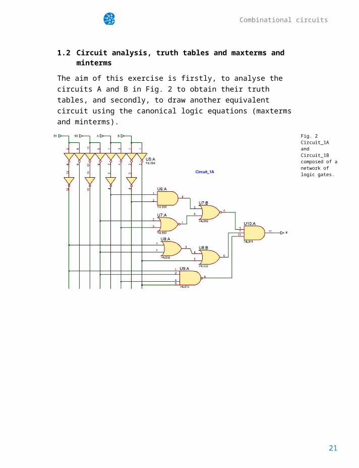
1.2 Circuit analysis, truth tables and maxterms and minterms
The aim of this exercise is firstly, to analyse the circuits A and B in Fig. 2 to obtain their truth tables, and secondly, to draw another equivalent circuit using the canonical logic equations (maxterms and minterms).
Fig. 2Circuit_1A and Circuit_1B composed of a network of logic gates.
18

Combinational circuits
Let us layout a plan to solve this problem:
1. Deduce the logic equations that exactly match the circuits.2. Apply Boolean algebra to determine the truth table (which is
equivalent to the sum of minterms and the product of maxterms). The numerical engine WolframAlpha1 can be used to verify the truth table typing directly the general equation and analysing the computer results.
3. Draw the circuits of the outputs P and Q and capture the schematics in Proteus and run simulations to verify the whole truth table.
4. Or, instead, run a VHDL design flow using EDA tools (a single-file structural project, circuit synthesis and test bench simulation) to generate a circuit and verify it by means of a timing diagram from which to annotate a truth table that has to be identical to the one deduced in 2).
The Fig. 3 represents several ways to plan the exercise of determining the truth table of a given simple combinational circuit composed of logic gates.
Fig. 3Multiple planning paths to analyse a circuit of logic
gates.
1 http://digsys.upc.es/csd/P01/P1_T/WolframAlpha/WolframAlpha.html
19
Problems on digital circuits and systems
Some ideas on the solution of this analysis problem can be found in this tutorial.
20

Combinational circuits
1.3 A variation: SoP and PoS Design the Problem 1.2 using sum of products (SoP) and product of sums (PoS) which are the minimised equations obtained from the truth table using an application like Minilog or Logic Friday.
1.4 Circuits using only NOR or only NAND Given the following Boolean expression:
Q=f ( x , y , z )=x · y+ y ' · z
a) Draw the circuit’s truth table and symbol. Represent the circuit using only NAND logic gates.
b) Express the output as a sum of minterms and a product of maxterms.
c) Using the equation obtained in b), represent the circuit using only-NOR logic gates.
d) If the propagation delays tPHL and tPLH of a gate of this kind, for instance, 74HCT technology is 21 ns, calculate the maximum frequency of operation of this circuit.
e) How would you use the VHDL simulator to verify the truth table of this digital circuit?
21

Problems on digital circuits and systems
1.5 Circuits using only NOR or only NAND Interpret the following table output format in Fig. 1 from Minilog. Draw the symbol of the circuit. Draw the logic circuit for the output A_L = f1 (D, C, B, A) using only NOR gates, and draw the circuit for the output B_L = f2 (D, C, B, A) using only NAND gates.
Fig. 4Output table
format from a given circuit described in
Minilog.
MINIMIZATION RESULT STATISTICS ==============================
FOUND 28 ESSENTIAL FACTORS IN PRODUCT OF SUMS MODE
MAXIMUM FANIN: 18
TOTAL LITERAL COUNT: 102
MAXIMUM FACTOR SIZE: 3
MAXIMUM OUTPUT FUNCTION SIZE: 6
Note: Remember that before drawing circuits you must deduce the equivalent equations
===========
ABE
DCBA LLL
===========
011- | 1..
10-0 | 1..
-1-1 | 111
0--1 | 1..
1-0- | 1..
-00- | 1..
11-- | .1.
0-10 | .1.
1-0 | .1.
1-11 | .1.
22

Combinational circuits
P2 Standard logic circuits: encoders, decoders, multiplexers, etc. After studying the content of these projects, you will be able to:
Design and use standard combinational logic blocks: multiplexers (or data selectors), demultiplexers (or data distributors), decoders, encoders, hexadecimal to seven-segment LED displays adapters, code converters, adders, comparators, etc.
Explain the concepts of flat and hierarchical designs and implement simple projects involving several components.
Use the method of decoders and the method of multiplexers to implement logic functions.
23

Problems on digital circuits and systems
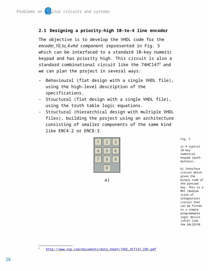
2.1 Designing a priority-high 10-to-4 line encoderThe objective is to develop the VHDL code for the encoder_10_to_4.vhd component represented in Fig. 5 which can be interfaced to a standard 10-key numeric keypad and has priority high. This circuit is also a standard combinational circuit like the 74HC1472 and we can plan the project in several ways:
- Behavioural (flat design with a single VHDL file), using the high-level description of the specifications.
- Structural (flat design with a single VHDL file), using the truth table logic equations.
- Structural (hierarchical design with multiple VHDL files), building the project using an architecture consisting of smaller components of the same kind like ENC4:2 or ENC8:3.
a)
0123456789
R910k VCC
GAL22V10
ENCODER_10_4
K0_LK1_LK2_LK3_LK4_LK5_LK6_LK7_LK8_LK9_L
GS
X3X2X1X0
(priority high)
0000
0
b)
Fig. 5
a) A typical 10-key numerical keypad (push-buttons).
b) Interface circuit which gives the binary code of the pressed key. This is a MSI (medium scale of integration) circuit that can be fitted in a simple programmable logic device (sPLD) like the GAL22V10.
1) Fill in the truth table using the names and the variable order depicted in the following table using “don’t care” (“-“or “x”) terms. GS has to be high
2 http://www.nxp.com/documents/data_sheet/74HC_HCT147_CNV.pdf
24

Combinational circuits
(‘1’) when any key is pressed and low (‘0’) otherwise. How many combinations does the truth table include?
K0_L
K1_L
K2_L
K3_L
K4_L
K5_L
K6_L
K7_L
K8_L
K9_L
X3
X2
X1
X0
GS
Comments
2) Draw the sketch of a timing diagram for the circuit commenting the outputs that are expected when applying different inputs.
3) How many minterms will X3 have? How many maxterms will X2 have?
4) By inspection of the truth table or using Minilog3, represent the five output functions either as sum of products (SoP) or product of sums (PoS).
5) Draw the logic circuit of the output X1 using only NOR gates. [(x·y)’= x’ + y’], [ (x·y·z)’’ = (x’ + y’ + z’)’ ]
6) If the propagation delay of a single gate of the technology used is 7.5 ns, which is the maximum frequency of operation of the circuit in 5)?
7) Find in internet a commercial standard circuit in classic technologies which has a similar truth table.
Optional questions related to synthesising the project encoder_10_to_4.vhd into a programmable device and testing it using EDA tools. The plan to organise the architecture is either 8), 9) or 10). 8) Architecture #1 (structural-flat): Write down the structural VHDL code
which is derived from the equations deduced in 4).
9) Architecture #2 (behavioural): Search Internet or find in books on the subject the high-level or algorithmic VHDL code for the component in Fig. 5b. As usual, use flow charts or schematics to translate the truth table into VHDL.
10) Architecture #3 (structural-hierarchical): Figure out how can be designed an ENC10:4 using components like ENC4:2 and other circuits if necessary. How many VHDL files will the project contain?
11) Create a design project for a CPLD or FPGA target chip, using EDA tools (ispLEVER Classic, Diamond, Quartus or ISE).
3 http://digsys.upc.es/ed/CSD/units/Ch1/U1_08/Unit1_8.html
25

Problems on digital circuits and systems
12) Translate the timing diagram sketch represented in 2) into a VHDL test bench file to functionally simulate the circuit using ActiveHDL, ModelSim or ISIm.
13) Perform a gate-level simulation to measure the worst case propagation delay and calculate the encoder’s maximum frequency of operation for a given PLD target chip.
26
Combinational circuits
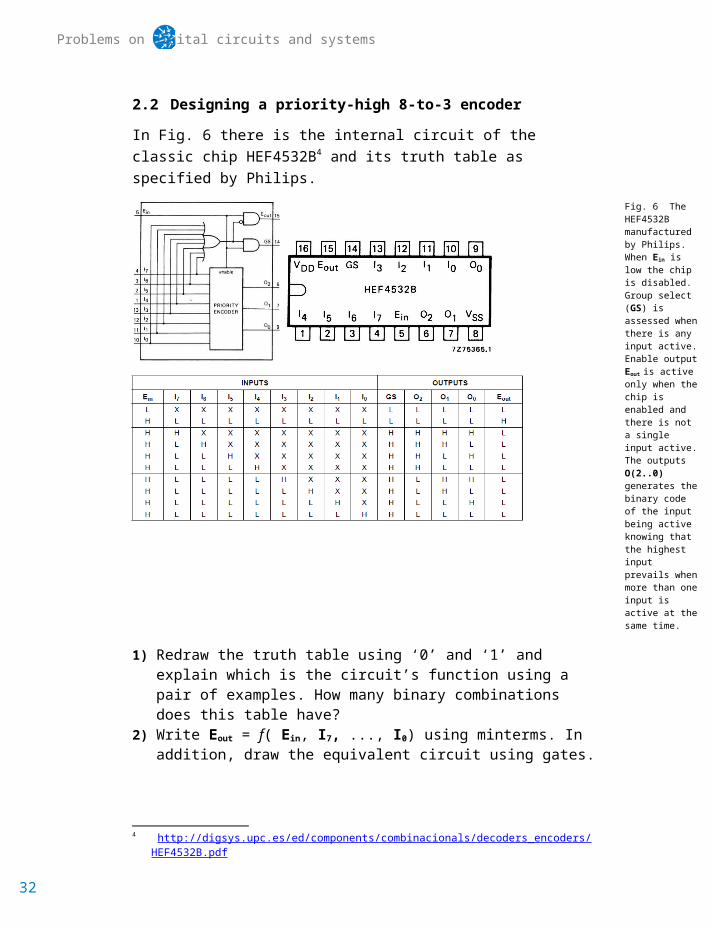
2.2 Designing a priority-high 8-to-3 encoderIn Fig. 6 there is the internal circuit of the classic chip HEF4532B4 and its truth table as specified by Philips.
Fig. 6 The HEF4532B manufactured by Philips. When Ein is low the chip is disabled. Group select (GS) is assessed when there is any input active. Enable output Eout is active only when the chip is enabled and there is not a single input active. The outputs O(2..0) generates the binary code of the input being active knowing that the highest input prevails when more than one input is active at the same time.
1) Redraw the truth table using ‘0’ and ‘1’ and explain which is the circuit’s function using a pair of examples. How many binary combinations does this table have?
2) Write Eout = f( Ein, I7, ..., I0) using minterms. In addition, draw the equivalent circuit using gates.
3) Write GS as a product of sums (PoS). How many minterms does this function have? Draw the circuit using gates.
Write O2 as a sum of products (SoP). How many maxterms does this function have? Write O1 and O0 as a product of sums (PoS).
4) Describe the circuit in VHDL in a behaviour or structural fashion. 5) Draw a sketch of a timing diagram and translate it into a test bench to be
able to verify the circuit using an EDA tool.
Optional questions related to further understanding the problem and designing the project encoder_8_to_3.vhd into a programmable device. 6) Write the .tbl format file so that it can be used to obtain the PoS or the
SoP in Minilog software. Find and write down the link to a similar circuit in
4 http://digsys.upc.es/ed/components/combinacionals/decoders_encoders/HEF4532B.pdf
27

Problems on digital circuits and systems
HADES which can be executed using the JAVA applet. Simulate the circuit in Proteus and check if it works as expected.
7) Start a VHDL-based synthesis project and a testbench-based simulation using EDA tools for target CPLD or FPGA programmable chips.
28

Combinational circuits
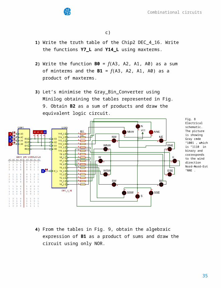
2.3 A digital wind direction meter We want to design a digital wind direction meter as seen in Fig. 7 based on an optoelectronic rotary encoder of 16 positions. The sensor disk, as shown in Fig. 7c, is coded in Gray, which was originally used instead of binary code to prevent spurious output from electromechanical switches. In Fig. 8 you can see the complete electrical schematic. We want to have both, a 4-bit binary output and a 1-bit coded output (one-hot) to light a circle of 16 LED to display the wind direction.
Fig. 7 a) Wind compass
describing the sixteen principal bearings used to
measure wind direction, b) the
wind transducer, and c) the basics
of the Gray to binary rotary
encoder sensor.
a) b)
c)
1) Write the truth table of the Chip2 DEC_4_16. Write the functions Y7_L and Y14_L using maxterms.
29

Problems on digital circuits and systems
2) Write the function B0 = f(A3, A2, A1, A0) as a sum of minterms and the B1 = f(A3, A2, A1, A0) as a product of maxterms.
3) Let’s minimise the Gray_Bin_Converter using Minilog obtaining the tables represented in Fig. 9. Obtain B2 as a sum of products and draw the equivalent logic circuit.
Fig. 8 Electrical schematic. The picture is showing Gray code “1001”, which is “1110” in binary and corresponds to the wind direction Nord-Nord-Est “NNE”.
4) From the tables in Fig. 9, obtain the algebraic expression of B1 as a product of sums and draw the circuit using only NOR.
5) Plan and draw a hierarchical circuit using the method of decoders and the Chip2 DEC_4_16, for the functions B2 and B1 of the Chip1. How many files the VHDL project will contain?
6) Write the VHDL code for the DEC_4_16 using a structural style (gates) (not all the code but a portion sufficient to show how the VHDL entity and architecture is organised).
Extra:
7) Synthesise the project using an EDA tool and test it using a VHDL test bench.
30
Combinational circuits
Fig. 9 Table output from MInilog when minimising the Gray_Bin_Converter Chip1. a) Sum of products (SoP), b) PoS.
Problem discussion
31
Problems on digital circuits and systems
2.4 Methods of decoders and multiplexers The following function is expressed in SoP:
f (w , x , y , z)= x' y ' z+x' y ' z '+wx y '+wy z '+xy
a) Draw the entity’s symbol and draw the circuit diagram using logic gates. Write the equation in VHDL.
b) Apply Boole Algebra analysis or use a computer tool like WolframAlpha or Logic Friday to deduce the truth table and the canonical equations sum of minterms and product of maxterms.
c) Solve the circuit by the method of multiplexers using a MUX4. How many VHDL files are required to implement the project of this circuit?
d) Solve the circuit by the method of decoders.e) Invent a timing diagram to demonstrate how the circuit works, and
translate it into a VHDL test bench to perform an ActiveHDL / ModelSim / ISim functional simulation.
32

Combinational circuits
P3 Arithmetic circuits: adders, multipliersAfter studying the content of these projects, you will be able to:
Design and use standard arithmetic blocks: adders Apply flat and hierarchical design to plan arithmetic circuits Design hardware multipliers
33
Problems on digital circuits and systems
3.1 Ripple adder(modify the problem so that it is a simple ripple-carry of n-bits)
Basic operations in two’s complement (2C) and 6 bits. Indicate the result and the value of the overflow flag after performing the operations:
a) Addition: (+16) + (-21) b) Subtraction: (-13) - (-27)c) Subtraction: (-9) - (+26)d) Addition: (-31) + (-31)
Invent and draw an entity named Adder_Subtractor_6bit that includes overflow (OV) and zero (Z) flags and propose its internal architecture using Adder_1bit components and logic gates.
e) Explain with some example vectors how your architecture works. f) How many VHDL files your circuit contains?
With reference to the component Adder_1bit:
g) Write the truth table of the Adder_1bit component (A i, Bi, Ci, Co, So). h) Implement Co using only NOR gates. i) Implement So using maxterms. j) If a logic gate has a propagation delay of 6.5 ns, deduce the maximum
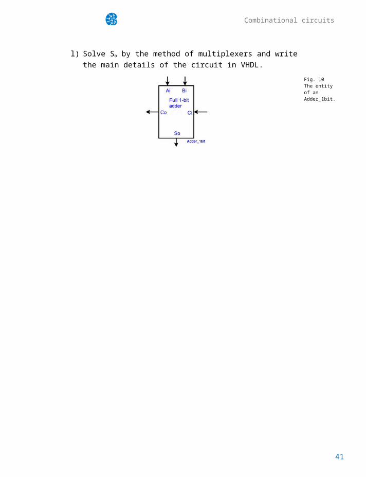
frequency of operation of your circuit. k) Solve Co by the method of decoders.l) Solve So by the method of multiplexers and write the main details of
the circuit in VHDL.
34

Combinational circuits
Fig. 10 The entity of an Adder_1bit.
35

Problems on digital circuits and systems
3.2 8-bit adder using 4-bit carry-lookahead adders(modify and delete sections so that it is a simple adder)
Basic addition and subtraction operations in two’s complement (2C) and 8 bits.
a) Indicate the result and the value of the overflow flag after performing the operations:
o Addition: (-100) + (-15) o Subtraction: (+100) - (+6)o Subtraction: (+6) - (-127)o Addition: (-127) + (-100)
Invent and draw an entity named Adder_Subtractor_8bit that includes overflow (OV) and zero (Z) flags and propose its internal architecture using 4-bit carry-lookahead adder components as shown in Fig. 11 and logic gates.
b) Explain with some of the previous vectors how your architecture works. Draw a timing diagram sketch.
c) How many VHDL files your circuit contains if build hierarchically? Name them all.
d) If a logic gate in Fig. 11 has a propagation delay of 12.5 ns, deduce the maximum frequency of operation of your circuit. How to perform such measurement using a VHDL simulator?
Development of the 4-bit lookahead adder.
e) Write the truth table of the output C1. f) Implement C1 using only NAND gates. g) Solve C1 by the method of multiplexers and write the main details of
the circuit in VHDL.h) Write the VHDL code of the complete 4-bit carry lookahead adder
(Adder_1bit.vhd, Adder_4bit.vhd, Carry_generator.vhd). i) Write the VHDL code of the complete system and name it
Adder_Subtractor_8bit.vhd.
36

Combinational circuits
Fig. 11The idea of a 4-bit
carry-lookahead adder (chip
74HCT283), as explained in:
Introduction to digital systems, Ercegovac, M.,
Lang, T., Moreno, J. H., John Wiley
& Sons, 1999, web.
Development of the 4-bit carry lookahead adder.
j) Start a project using an EDA tool and synthesise the circuit in a given target chip CPLD or FPGA. Print the RTL view and commend it.
Test the 4-bit carry lookahead adder.
k) Start a VHDL simulator EDA tool and run a test bench to verify the unit under test applying some 4-bit operands. Print the timing diagram and add notes and explanations.
Development of the 8-bit adder/subtractor.
l) Start a project using an EDA tool and synthesise the circuit in a given target chip CPLD or FPGA. Print the RTL view and commend it.
Test the 8-bit adder/subtractor.
m) Start a VHDL simulator EDA tool and run a test bench to verify the unit under test (UUT) applying some 8-bit positive and negative integers
37

Problems on digital circuits and systems
like the ones in a). Print the timing diagram and add notes and explanations to analyse the result.
n) Measure the maximum speed of operation (or computation or data processing) of the circuit using a gate-level simulation. Print the timing diagram explaining how the measurements are made in a given signal transition. Explain the data from the time analyser tool.
o) Can you compare result with an 8-bit adder/subtractor solved using 4-bit ripple carry adders?
3.3 8-bit ones counter The idea is in this former problem. (ref.)
38

Combinational circuits
3.4 1-bit subtractor We want to implement a circuit for subtracting 8-bit binary numbers as represented in Fig. 12.
D = A – B
0 ≤ A, B ≤ 2n – 1
A B
Fig. 12 The entity of an Onebit_subtractor
The strategy is to use a chain of simple 1-bit subtractors instead of the typical 1-bit adders and the two’s complement convention. Thus, the circuit will work only with positive integers. The Fig. 13 shows the building block.
0 − 0 → 0
0 − 1 → 1, borrow 1
1 − 0 → 1
1 − 1 → 0
Fig. 13 The entity of an Onebit_subtractor
So, we can chain many 1-bit subtractor connecting the “borrows” in the same way we connect the “carry” when adding:
* * * * (starred columns are borrowed from)
1 1 1 0 1 1 1 0 A(7..0) (238)
− 1 0 1 1 1 - B(7..0) - ( 23)
---------------- ------- ------
= 1 1 0 1 0 1 1 1 D(7..0) (215)
The full 1-bit subtractor (SUB_1) have the following truth table: D = f(A, B, Bin) = ∑m( 1, 2, 4, 7); Bout = g(A, B, Bin) = ∏M(0, 4, 5, 6)
1. Representing the truth table by means of equations, implement the 1-bit subtractor using only NAND gates. Write the equations in VHDL.
2. Write the code for the 1-bit subtractor in VHDL using a behavioural approach.
39
Problems on digital circuits and systems
3. Draw the schematic of the 8-bit ripple subtractor (SUB_8) and describe it in VHDL using components.
4. Implement the logic circuit of a pair of flags or indicators to detect special events like:
A zero result D = A – B = 0)
A negative number D < 0 (A<B)
5. Draw a sketch of a timing diagram and write it as a VHDL test bench to test your design. Try at least three operations:
A = 230, B = 45; A = 187, B = 177; A = 177, B = 187
40

Combinational circuits
P4 Arithmetic circuits: two’s complement, subtraction, comparisonAfter studying the content of these projects, you will be able to:
Design and use standard arithmetic blocks: subtractors, comparators, etc.
Solve arithmetic operations in two’s complement format (2C). Design simple combinational circuits in a hierarchical way using
multiple combinational circuits as components. Solving problems using different approaches and comparing solutions.
41

Problems on digital circuits and systems
4.1 Addition and subtraction in two’s complement1. Draw the symbol and the internal schematic of a 6-bit two’s complement
adder/subtractor and determine the range of the operants and the result. Explain how the overflow (OV) flag works.
2. Perform the following operations in binary using the two’s complement (2C) 6-bit adder/subtractor from previous section 1). Check the result and deduce the Z and OV flags.
a) (+26)10 + (101010)2C
b) (101010)2C - (-21)10
c) (+18)10 + (101110)2C
d) (-31)10 - (010110)2C
3. Represent the previous operations in a timing diagram and translate it (only the stimulus section) to a VHDL test bench using a constant Min_Pulse = 7.5 µs.
4. Determine the maximum speed of operation of the 6-bit 2C adder/subtractor if synthesised in a Xilinx technology Coolrunner CX2C256 CPLD that has the propagation delays shown below. Justify your calculations.
Problem discussion
42

Combinational circuits
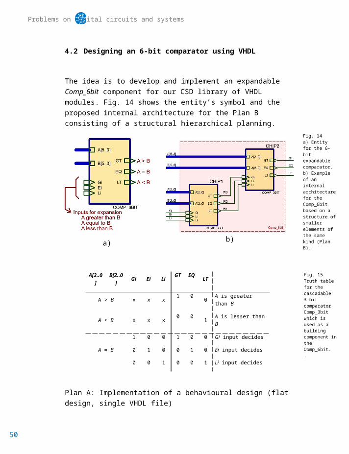
4.2 Designing an 6-bit comparator using VHDL The idea is to develop and implement an expandable Comp_6bit component for our CSD library of VHDL modules. Fig. 14 shows the entity’s symbol and the proposed internal architecture for the Plan B consisting of a structural hierarchical planning.
a) b)
Fig. 14 a) Entity for the 6-bit expandable comparator. b) Example of an internal architecture for the Comp_6bit based on a structure of smaller elements of the same kind (Plan B).
A[2..0]
B[2..0] Gi Ei Li GT EQ LT
A > B x x x 1 0 0 A is greater than B
A < B x x x 0 0 1 A is lesser than B
1 0 0 1 0 0 Gi input decides
A = B 0 1 0 0 1 0 Ei input decides
0 0 1 0 0 1 Li input decides
Fig. 15 Truth table for the cascadable 3-bit comparator Comp_3bit which is used as a building component in the Oomp_6bit..
Plan A: Implementation of a behavioural design (flat design, single VHDL file)
a) Explain the design flow you will follow to produce your circuit using EDA tools like Lattice ispLEVER Classic / Altera Quartus II / Xilinx ISE. Draw the truth table and a timing diagram sketch for the Comp_6bit circuit.
43

Problems on digital circuits and systems
b) Write down the high level or behavioural VHDL code directly as a single block as in Fig. 14a planning writing first an algorithm or a flowchart to translate the circuit’s truth table.
c) Create a single-file VHDL project using the EDA tools to synthesise a circuit for a simple programmable logic device (sPLD) GAL22V10 (24 pins) or a CPLD or a FPGA chip. Print and comment the RTL and the technology views of the synthesised circuits.
d) Test and simulate your design using Proteus and its EasyHDL scripting language (in case of a sPLD). Or, in case of a target chip CPLD or FPGA, use ActiveHDL / ModelSim / ISim simulators by means of a VHDL test bench, thus, translating the timing diagram sketch into VHDL to apply input stimulus. Print the timing diagrams and comment them.
Plan B: Implementation of a structural design in a CPLD or a FPGA.
a) Explain the design flow you will follow to produce your circuit using Lattice ispLEVER Classic / Altera Quartus II / Xilinx ISE.
b) Draw a structured hierarchical design as in Fig. 14b using several components. For instance, Fig. 15 shows the truth table for a 3-bit cascadable comparator.
c) Implement the elemental Comp_1bit using the logic equations derived from Minilog.exe (single output mode, sum of products, table output format). Verify your equations using WolframAlpha.
d) Create a multiple-file VHDL-based project using EDA tools for a CPLD target chip, for example: Lattice ispMACH4128V TQFP100, or the Intel-Altera MAX EPM7128SLC84-7, or the Xilinx CoolRunner II XC2C256-TQ144 - 7. Print the RTL and technology views of the synthesised circuit, so that it can be compared to the initial block diagram proposed in Fig. 14b.
e) Test and simulate your design using the ActiveHDL / ModelSim / ISim simulators by means of a VHDL test bench.
(Optional)
44

Combinational circuits
f) Assign pins and generate the output configurations files if the circuit has to be prototyped in a development board (Lattice HWD-LC4128V, Altera UP2 or Xilinx CoolRunner-II CPLD Starter Board).
g) Write down a report to document your design using our quality standards and templates.
45

46
2

Sequential systems
47

Problems on digital circuits and systems
P5 1-bit memory cellsAfter studying the content of these projects, you will be able to:
Deduce a data flip-flop DFF from an RS latch Analyse asynchronous circuits
5
48
Sequential systems
5.1 Designing and using a RS latch
49

Problems on digital circuits and systems
5.2 Set-Reset flip flop (RS-FF)Follow this tutorial on how to implement an RS-FF from a RS latch.
50

Sequential systems
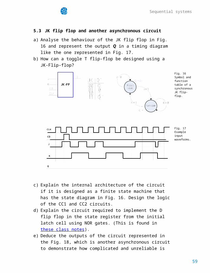
5.3 JK flip flop and another asynchronous circuita) Analyse the behaviour of the JK flip flop in Fig. 16 and represent the
output Q in a timing diagram like the one represented in Fig. 17. b) How can a toggle T flip-flop be designed using a JK-Flip-flop?
Fig. 16 Symbol and function table of a synchronous JK flip-flop.
Fig. 17 Example input waveforms.
c) Explain the internal architecture of the circuit if it is designed as a finite state machine that has the state diagram in Fig. 16. Design the logic of the CC1 and CC2 circuits.
d) Explain the circuit required to implement the D flip flop in the state register from the initial latch cell using NOR gates. (This is found in these class notes).
e) Deduce the outputs of the circuit represented in the Fig. 18, which is another asynchronous circuit to demonstrate how complicated and unreliable is the asynchronous design in front of the synchronous canonical design based on FSM.
51

Problems on digital circuits and systems
Fig. 18 Example of an asynchronous circuit.
52

Sequential systems
5.4 Toggle flip flop (T-FF)Design a T-FF using the FSM strategy. Follow this tutorial.
53

Problems on digital circuits and systems
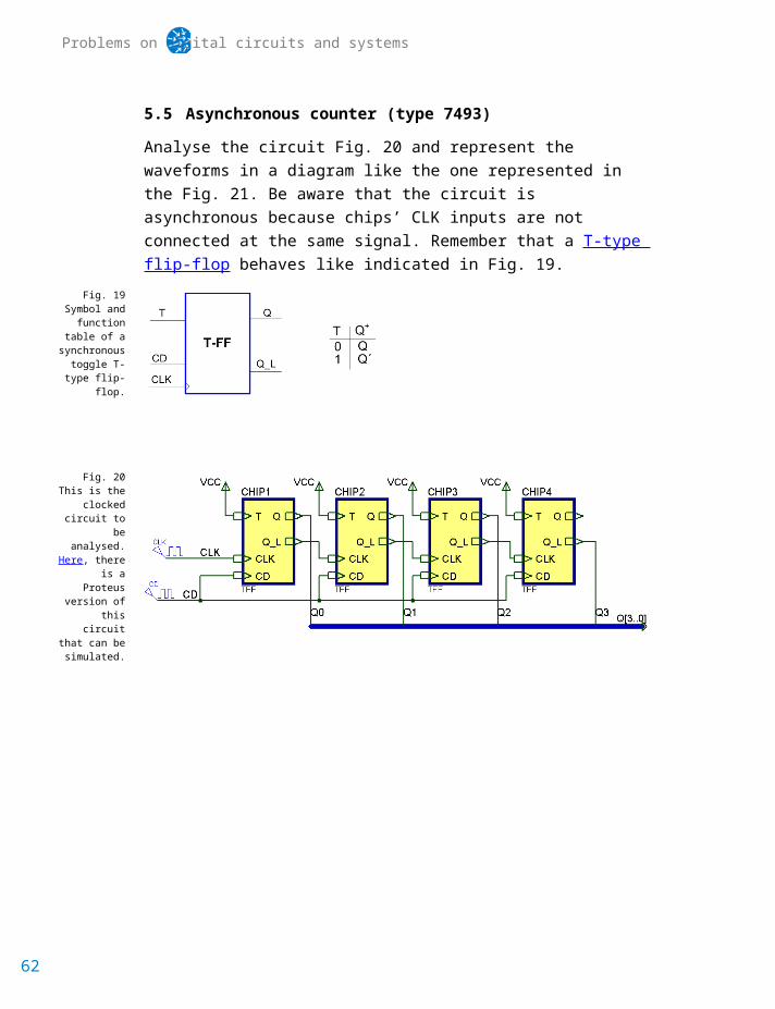
5.5 Asynchronous counter (type 7493) Analyse the circuit Fig. 20 and represent the waveforms in a diagram like the one represented in the Fig. 21. Be aware that the circuit is asynchronous because chips’ CLK inputs are not connected at the same signal. Remember that a T-type flip-flop behaves like indicated in Fig. 19.
Fig. 19Symbol and
function table of a synchronous
toggle T-type flip-flop.
Fig. 20This is the clocked
circuit to be analysed. Here,
there is a Proteus version of this
circuit that can be simulated.
Fig. 21Output
waveforms to be
deduced from the
circuit in Fig.20.
54

Sequential systems
Which is the circuit function? What will be the circuit applied for? Which is the circuit’s main problem, so that it has to be discarded for precision applications?
A VHDL design tutorial of a similar circuit can be found here.
55

Problems on digital circuits and systems
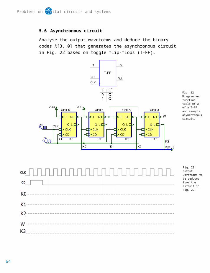
5.6 Asynchronous circuit Analyse the output waveforms and deduce the binary codes K[3..0] that generates the asynchronous circuit in Fig. 22 based on toggle flip-flops (T-FF).
Fig. 22 Diagram and function table of a of a T-FF and example asynchronous circuit.
Fig. 23 Output waveforms to be deduced from the circuit in Fig. 22.
A draft solution of the problem can be consulted here.
56

Sequential systems
P6 Finite State Machines (FSM)After studying the content of these projects, you will be able to:
Design simple FSM using a systematic methodology
6
57
Problems on digital circuits and systems
6.1 Controlling the classroom luminaires This is the light control (Light_Control) tutorial to introduce the FSM basic concepts.
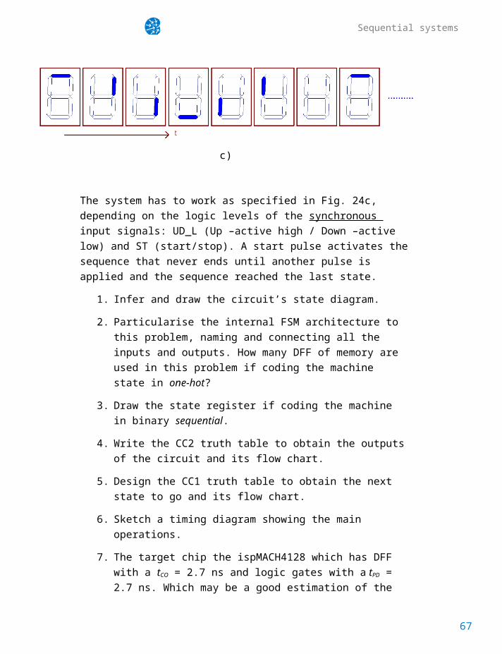
6.2 7-segment digit sequencer We want to design a simple driver to shown a sequence of movement, clockwise and counter-clockwise, in a single 7-segment display. Fig. 24 represents the schematic diagram of the application. The circuit components are: (1) a clock to produce a rectangular wave with a given frequency, let us take 5 Hz; (2) the digital system; and (3) the 7-segment display (common cathode) with its current-limiting resistors.
a)
Fig. 24 a) Block diagram of the circuit. b) Digit segments and position when idle. c) Sequence of switching LED segments for UD_L = ‘1’ (up).
b)
c)
58

Sequential systems
The system has to work as specified in Fig. 24c, depending on the logic levels of the synchronous input signals: UD_L (Up –active high / Down –active low) and ST (start/stop). A start pulse activates the sequence that never ends until another pulse is applied and the sequence reached the last state.
1. Infer and draw the circuit’s state diagram.
2. Particularise the internal FSM architecture to this problem, naming and connecting all the inputs and outputs. How many DFF of memory are used in this problem if coding the machine state in one-hot?
3. Draw the state register if coding the machine in binary sequential.
4. Write the CC2 truth table to obtain the outputs of the circuit and its flow chart.
5. Design the CC1 truth table to obtain the next state to go and its flow chart.
6. Sketch a timing diagram showing the main operations.
7. The target chip the ispMACH4128 which has DFF with a tCO = 2.7 ns and logic gates with a tPD = 2.7 ns. Which may be a good estimation of the maximum frequency if operation? Explain your answer.
8. Design a circuit to produce the 5 Hz square wave from a 10 MHz quartz crystal oscillator and deduce the number of DFF that will contain.
This is an initial discussion in class.
59

Problems on digital circuits and systems
6.3 1-digit BCD counter (flat, like a FSM)This is the design of a 1-digit BCD counter using a flat design based on the adaptation of a FSM
60
Sequential systems
6.4 Traffic light controller
7
61

Problems on digital circuits and systems
P7 Standard counters and registers After studying the content of these projects, you will be able to:
Design standard counter and registers Design applications based on registers and counters
7.1 1-digit BCD counter (flat)This is the design of a 1-digit BCD counter using a flat design based on the use of arithmetic circuits.
7.2 1-digit BCD counter (hierarchical)This is the design of a 1-digit BCD counter using a hierarchical design based on a Counter_mod16 component.
62
Sequential systems
7.3 Synchronous universal 4-bit binary counterOur goal is to design as a FSM the building block used in the previous 7.8 problem. It is a synchronous, presettable (LD, parallel load), 4-bit (modulo 16), reversible (up and down), binary counter with count enable (CE) and terminal count (TC16) as represented in Fig. 25. It is a chip similar to the classic 74LS169.
LD CE UD_L Q+ Synchronous operation after the CLK’s rising edge
1 x x Din Parallel load (register data)
0 0 x Q Do nothing (inhibit)
0 1 1 (Q+1)mod16 Up counting in binary
0 1 0 (Q-1)mod16 Down counting in binary
TC16 = ‘1’ when CE = ‘1’ and [(Q = 15 and UD_L = ‘1’) or (Q = 0 and UD_L = ‘0’)]; ‘0’ otherwise
Fig. 25Synchronous 4-bit universal binary counter. Symbol and function table. This is an example Proteus simulation of a very similar circuit.
Specifications
1. Symbol, function table, example of a timing diagram, state diagram. How many states this sequential system must have?
Planning
1. Customise the general FSM architecture for this problem indicating where every input and output is connected. Plan the circuit as a FSM in a single VHDL file.
2. How many data flip-flops (DFF) are required? Draw the schematic of the state register. Which is the internal encoding the current_state signal
3. Name the circuit Counter_mod16 and plan the circuit as a FSM in a single VHDL file.
4. Write the truth table for the CC2 and propose an internal circuit. 5. Write the truth table for the CC1 and propose an internal circuit. Draw
the truth table’s flow chart as the behavioural interpretation.
Developing
63

Problems on digital circuits and systems
6. Translate the circuit schematic to VHDL and start an EDA project to synthesise it for a given CPLD/FPGA target chip.
7. Inspect and analyse the RTL view and technology schematics. Check the number of DFF registers.
Test
8. Run a functional simulation translating the timing diagram into a VHDL test bench.
9. Run a gate-level simulation and determine propagation time from CLK to output (tCO) and thus, the maximum frequency of operation for the given target chip.
Problem discussion and project files.
This picture is an example of a functional simulation of the universal counter modulo 16. The comments in red ink are very important to check whether the circuit works as expected.
64

Sequential systems
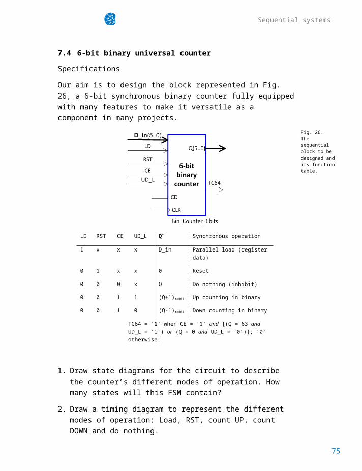
7.4 6-bit binary universal counter Specifications
Our aim is to design the block represented in Fig. 26, a 6-bit synchronous binary counter fully equipped with many features to make it versatile as a component in many projects.
Fig. 26. The sequential block to be designed and its function table.
LD RST CE UD_L Q+ Synchronous operation
1 x x x D_in Parallel load (register data)
0 1 x x 0 Reset
0 0 0 x Q Do nothing (inhibit)
0 0 1 1 (Q+1)mod64 Up counting in binary
0 0 1 0 (Q-1)mod64 Down counting in binary
TC64 = ‘1’ when CE = ‘1’ and [(Q = 63 and UD_L = ‘1’) or (Q = 0 and UD_L = ‘0’)]; ‘0’ otherwise.
1. Draw state diagrams for the circuit to describe the counter’s different modes of operation. How many states will this FSM contain?
2. Draw a timing diagram to represent the different modes of operation: Load, RST, count UP, count DOWN and do nothing.
Planning as a FSM in a single VHDL file
3. Draw the architecture of the FSM particularised for this problem and indicate where all the inputs and outputs are connected.
65
Problems on digital circuits and systems
4. How many registers (D-type flip-flops) will the system include? Explain your answer.
5. Draw the truth table and flow chart of the combinational circuit CC1
6. Draw the truth table and flow chart of the combinational circuit CC2.
Development using CAD/EDA tools
7. What is the synthesis process? In which way can we examine the result of the synthesis process?
Verification:
8. Write the main features of a test bench file “VHT” necessary to perform a functional simulation. For instance, translating to VHDL some vectors from the 2 section.
9. What are the “VHO” and the “SDF” files? Which is the use of these files? The target chip is the ispMACH4128V which has DFF with a tCO = 2.7 ns and logic gates with a tPD = 2.7 ns. Which may be a good estimation of the maximum frequency if operation? Explain your answer.
7.5 Data register Design a synchronous 12-bit data register using VHDL. Here you are a tutorial.
66

Sequential systems
7.6 Shift register Design a synchronous 8-bit universal shift register using VHDL. Here you are a tutorial.
67

Problems on digital circuits and systems
7.7 Synchronous modulo 12 counter Design as a complete project following the usual steps, the synchronous up/down modulo 12 counter represented in Fig. 27 using 2 different strategies. Compare and discuss the advantages and drawbacks of each strategy.
Fig. 27Synchronous
up/down binary counter modulo
12 with asynchronous
clear direct.
Project A. Single VHDL file (flat) FSM based on naming states and the use of State_type signals. Thus, using this methodology this project becomes simply another P6 FSM example.
Project B. Single VHDL file (flat) FSM based on the arithmetic VHDL library the use of std_logic_vector signals. Thus, using this methodology this project becomes another exercise like the Counter_mod16 in .
Project C. Hierarchical structure (multiple file project) based on the building block Counter_mod16 engineered in problem .
Plan A: Problem discussion and project files.
Plan B: Problem discussion and project files.
Plan C: Problem discussion and project files.
This picture is an example of a functional simulation of the counter module 12.
This picture is an example of a gate-level simulation of the counter module 12 for measuring the tCO propagation delay.
68

Sequential systems
7.8 Hour counter for a real-time clockOur goal is to design an hour counter to be used in a real-time clock device to count the hours in modes 0 – 12 (M = ‘1’) and 0 -24 (M = ‘0’). The Fig. 28 represents the schematic diagram of the application when connected to 7-segment digits.
Fig. 28Synchronous 2-digit BCD module 12/24 counter
Specifications
1. Explain the function table of the hour_counter discussing the different modes of operation.
2. Draw an example of timing diagram. How many states will the hour counter contain?
3. Draw the function table and symbol of a synchronous 4-bit binary universal counter (Counter_mod16).
Plan
4. Organize the internal architecture of the hour counter based on the use of universal 4-bit binary counters and combinational circuits and logic gates.
5. How many VHDL files will be required to complete the Hour_counter_top in Fig. 28?
Develop
6. Find the Counter_mod16.vhd file and translate the hierarchical schematic in Fig. 28 to VHDL.
69

Problems on digital circuits and systems
7. Start a synthesis project and inspect the RTL and technology views schematics. Check the project summary to verify the number of DFF. The target chip may be any CPLD or FPGA available in the laboratory.
Test
8. Translate the timing diagram in 2) to VHDL (Counter_mod16_tb.vhd) and run the functional test.
9. Run a gate level simulation and measure the tCO parameter and thus, the maximum speed of operation.
Prototype
10. Choose a laboratory experimentation board like the NEXYS 2 from Digilent. Assign pins and build and check the prototype Hour_counter_top adding the necessary chips and modifications. Pay attention on how the 7-segment digits are wired.
Hint: This is a reference to a circuit solved using the Proteus simulator where several counter modules are chained together to increment the counter’s capability. This is another reference on a full problem discussion.
Problem discussion and project files.
This picture is an example of a functional simulation of the Hour_counter working in the AM-PM mode (M = ‘1’)
70

Sequential systems
8P8 Dedicated processors and advanced circuitsAfter studying the content of these projects, you will be able to:
Design complex circuits based on datapath and control unit
71

Problems on digital circuits and systems
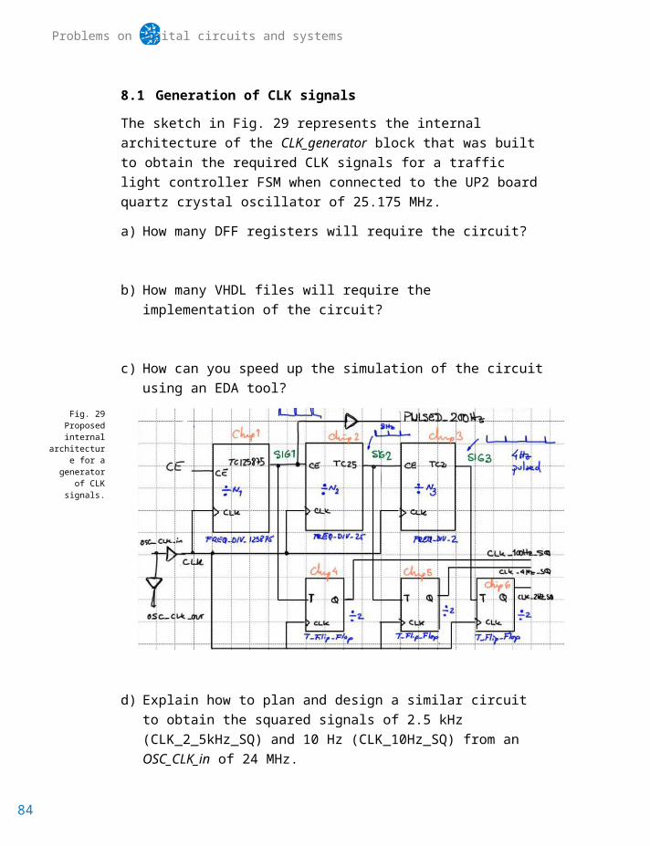
8.1 Generation of CLK signals The sketch in Fig. 29 represents the internal architecture of the CLK_generator block that was built to obtain the required CLK signals for a traffic light controller FSM when connected to the UP2 board quartz crystal oscillator of 25.175 MHz.
a) How many DFF registers will require the circuit?
b) How many VHDL files will require the implementation of the circuit?
c) How can you speed up the simulation of the circuit using an EDA tool?
Fig. 29Proposed internal architecture for a generator of CLK
signals.
d) Explain how to plan and design a similar circuit to obtain the squared signals of 2.5 kHz (CLK_2_5kHz_SQ) and 10 Hz (CLK_10Hz_SQ) from an OSC_CLK_in of 24 MHz.
e) Explain how to design a circuit like the Chip 2 FREQ_DIV_25 in Fig. 29 using VHDL and the FSM technique. Represent a timing diagram to show how it works.
72

Sequential systems
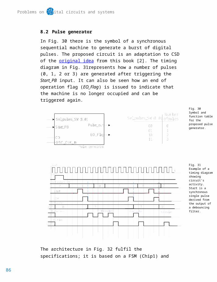
8.2 Pulse generatorIn Fig. 30 there is the symbol of a synchronous sequential machine to generate a burst of digital pulses. The proposed circuit is an adaptation to CSD of the original idea from this book [2]. The timing diagram in Fig. 31represents how a number of pulses (0, 1, 2 or 3) are generated after triggering the Start_PB input. It can also be seen how an end of operation flag (EO_Flag) is issued to indicate that the machine is no longer occupied and can be triggered again.
Fig. 30 Symbol and function table for the proposed pulse generator.
Fig. 31 Example of a timing diagram showing circuit’s activity. Start is a synchronous single pulse derived from the output of a debouncing filter.
The architecture in Fig. 32 fulfil the specifications; it is based on a FSM (Chip1) and other components. Why a component such a synchronous data register (Chip2) is necessary? Why a circuit like the debouncing filter (Chip4) is required to interface the Start push-button?
Explain the internal architecture of the Data_register_2bit component. How many states does it have? How many data flip-flops (DFF) are required to implement its state register?
73
Problems on digital circuits and systems
Infer the state diagram of the Pulse_Gen_FSM that may solve the sequence of operations to generate the outputs.
Draw the CC2 truth table and its flowchart interpretation, so that it can be coded in VHDL in the usual CSD style.
Fig. 32Sketch of an
internal architecture
for the system.
Draw the CC1 truth table and its flowchart interpretation, so that it can be coded in VHDL in the usual CSD style.
Draw the internal circuit of the state register. How many data flip-flops (DFF) are required to implement it if we encode the machine in binary (sequential), or alternatively in one-hot?
Write down the VHDL test bench translating approximately the inputs signals in the Fig. 31 diagram.
If the FPGA used as a target chip to synthesise the system has a worst-case time to output propagation delay (tCO) of 5.6 ns, which is the maximum CLK frequency and so the minimum pulse duration?
If the circuit uses a 16 MHz OSC_CLK_in from a quartz crystal, invent a CLK generator block to produce both square signals, a system CLK of 10 kHz and a 100 Hz signal to drive the debouncing circuit. How many VHDL files may it contain?
74

Sequential systems
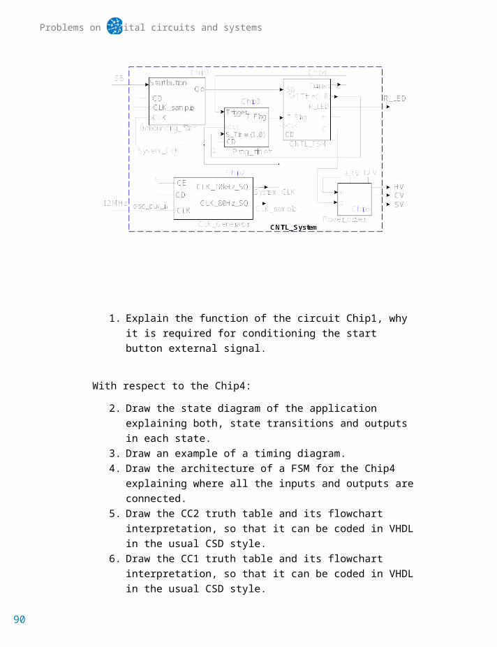
8.3 Designing an industrial application In a gym and fitness centre, there are some shower stalls like the one represented in Fig. 34 that have to be automated to generate cycles of contrasting hot (48 C), warm (26C) and cold (4C) water sprays simply clicking a single start push button (SB). After clicking the SB, initially warm water flows for 50 s (H = C = ‘1’), then hot water (H = ‘1’, C = ‘0’) for 10 s, and thirdly cold water (H = ‘0’, C = ‘1’) for 20 s, and this cycle is repeated another time; finally the system goes idle (H = C = ‘0’) to wait for another user service. During the operation the R_LED turns on and the water solenoid valve (SV) is on. Let us design the digital control system connected to the valves’ power driver (Chip5) using two technologies: a CPLD/FPGA and a microcontroller.
Fig. 33 Photograph and sketch of the shower installation to be automated.
75

Problems on digital circuits and systems
1. Explain the function of the circuit Chip1, why it is required for conditioning the start button external signal.
With respect to the Chip4:
2. Draw the state diagram of the application explaining both, state transitions and outputs in each state.
3. Draw an example of a timing diagram.4. Draw the architecture of a FSM for the Chip4 explaining where all the
inputs and outputs are connected. 5. Draw the CC2 truth table and its flowchart interpretation, so that it
can be coded in VHDL in the usual CSD style. 6. Draw the CC1 truth table and its flowchart interpretation, so that it
can be coded in VHDL in the usual CSD style. 7. Draw the internal circuit of the state register. How many bits and DFF
(data-type flip flops) will be used if the states are coded in one-hot?
With respect to the Chip3:
8. Explain the internal architecture, components and the number of VHDL files of the Prog_Timer project.
With respect to the Chip2:
9. Deduce and explain the internal architecture, the number of VHDL files and names of the CLK_Generator project.
10. We have measured by means of a gate-level VHDL simulation for the target CPLD/FPGA where the circuit is synthesised, a worst-case CLK to output propagation delay (tCO) of 6.3 ns. Thus, which is the maximum OSC_CLK_in frequency and so the minimum pulse duration?
76

Sequential systems
8.4 Synchronous serial adder This is the project to review and write as a problem: serial adder (ref.)
8.5 Synchronous serial multiplier This is the project to review and write as a problem: serial multiplier (ref.)
8.6 Serial transmitter and receiver (USART)This is the project to review and write as a problem: USART (ref.)
8.7 Steeping motor control based on a dedicated processor
This is the project to review and write as a problem: (ref.)
77

78
3

Microcontroller applications
9
P9 Combinational circuit solved using a microcontroller
After studying the content of this chapter on the basics of microcontrollers, you will be able to:
Explain the basic architecture of a 8-bit microcontroller …
9.1 The microcontroller PIC16FAnswer the following questions referred the microprocessors in general:
1. Explain the differences between Harvard (Microchip PIC) and Von Neumann (Intel 8051) microprocessor architectures. Draw the sketch of the architectures.
2. Which is the main architectural difference between 8/16/32 bits microprocessors?
3. Which are the functions of the FLASH (ROM) memory and the RAM registers?
4. Explain what the stack memory is and how it is used for.5. Describe the main blocks of the central process unit (CPU) and
how can you connect it to the content of the previous Chapters 1 and 2.
6. How an assembler instruction is executed? Find an example of C code disassembled and explain how it works.
7. How many clock cycles are required for executing an instruction in assembler?
79

Problems on digital circuits and systems
The architecture of the PIC16F87xA family is presented in Fig. 34. - Examine it and list the components that you could be able to design and
synthesise, if that were the case, into a PLD using VHDL and applying strategies from previous chapters.
- Can you redraw the architecture as a programmable dedicated processor to solving each machine-code instruction?
- Draw the blocks of the RAM and the ROM components and explain how to perform memory writing and reading operations.
- Find the specification of the Timer0 peripheral and compare them with the programmable timer designed in Chapter 2.
80
Microcontroller applications
Fig. 34 PIC16F87xA architecture.
81

Problems on digital circuits and systems
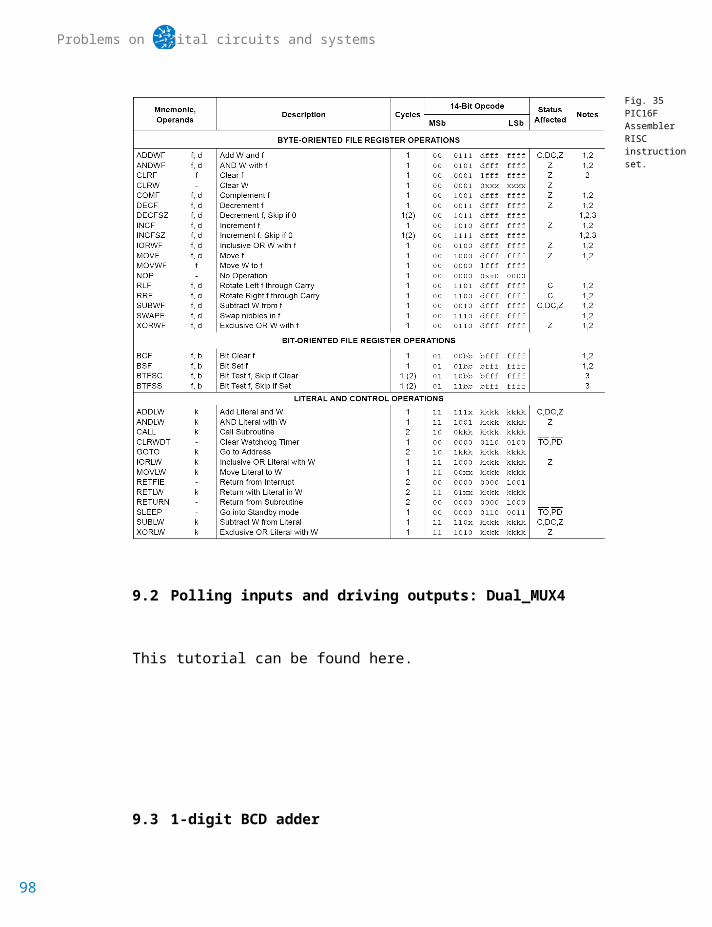
Fig. 35 PIC16F Assembler RISC instruction set.
9.2 Polling inputs and driving outputs: Dual_MUX4
This tutorial can be found here.
9.3 1-digit BCD adder
82
Microcontroller applications
10P10 Interrupts and FSM style programming using microcontrollers
After studying the content of this chapter on the basics of microcontrollers, you will be able to:
Explain …. …
10.18-bit Binary counter, event detection
10.21-digit BCD counter
11
83

Problems on digital circuits and systems
P11 Peripherals: LCD display
After studying the content of this chapter on the basics of microcontrollers, you will be able to:
Explain …. …
11.1Basic interface for a LCD display
11.2 Interfacing an I2C display
84
Microcontroller applications
12P12 Peripherals and more complex applications
After studying the content of this chapter on the basics of microcontrollers, you will be able to:
Explain …. …
85

Problems on digital circuits and systems
12.1 Industrial applicationThis problem is connected with Problem . The idea now is to design it using a microcontroller instead of a dedicated hardware design in VHDL. Read the assignment and solve the initial questions 1, 2, 3, 4.
Continue the problem as follows:
5. Draw the hardware schematic for an Atmel ATmega8535 microcontroller. Connect all the inputs and outputs to convenient I/O port pins, the reset button and the 12 MHz quartz crystal.
6. Architecture of the software. Organise and describe the program variables. Explain the use of interrupts. Assume that in a Phase #1 of the design, an external CLK signal of 4 Hz is available to generate the warm, hot and cold water timing periods of 50, 10 and 20 s respectively.
7. Describe the flowchart of bitwise operations for the functions to interface the hardware: read_inputs(), write_outputs() and ISR(interrupt service routine). What kind of operations are solved by the init_system() function?
8. Describe the truth table and flowchart of the function to solve the state transitions: state_logic().
9. Describe the truth table and flowchart of the function to implement the output variables: output_logic().
10. Explain how to implement the timing signal of 4 Hz s internally using the Timer0 counter/timer peripheral in a Phase #2 of the project.
86

Microcontroller applications
12.2Simple remote controlWe want to design a very simple wireless infrared remote control for an electronic equipment as shown in Fig. 36. In this initial stage of the design, the Chip1 is the microcontroller while the other components are external integrated circuits. The Chip2 (decoder BCD to 7-segments) is used to show the channel number, the Chip3 is the infrared transmitter, and the Chip4 is a 2 seconds CLK. Furthermore, the volume control is not implemented and thus only the buttons BU and BD are considered.
The system has a capacity of 7 channels. To increment the channel the BU (Channel up) has to be pressed. To decrement the channel number the BD (Channel down) has to be pressed. If both buttons are pressed or released simultaneously, the channel count is maintained. The buttons are sampled every 2 seconds (0.5 Hz). The outputs C(2..0) represents the channel selected in binary.
Fig. 36Schematic of a basic remote control for 7 channels. .
Design phase #1
1. Timing diagram.2. State diagram. The initial state is the Channel 1. 3. Hardware circuit. Connect input and output pins to the microcontroller
ATmega8535, a master reset and crystal oscillator of 8 MHz. 4. Architecture of the software. Program variables. Use of interrupts. 5. Functions to interface the hardware: init_system(), read_inputs(),
write_outputs(), ISR(source of interrupt). Flowchart of bitwise operations.6. The function to implement state transitions: state_logic(). Truth table and
flowchart.
87

Problems on digital circuits and systems
7. The function to implement the outputs: output_logic(). Truth table and flowchart.
Design phase #2
8. If we like to include into the microcontroller the functionality of the Chip2 (decoder BCD to 7-segments), so that this external chip will be no longer required, how to proceed?
9. If we like to include the Power_ON/OFF button into the microcontroller, so that when clicked the code “000” is generated immediately, how to proceed?
88
Microcontroller applications
12.3Timers. Simple remote control1. Specifications
Our aim is to design a timer of exactly 11.25 s as represented in Fig. 37. It is non-retriggerable, which means that the system is not affected even if you click the Trigger more than once while active in the timing period. In this project, the strategy will be to count external/internal pulses once the trigger signal is detected as represented in the timing diagram. The project is based on a PIC18F4520 microcontroller from Microchip. We will consider two design options and you have to choose one of them:
Option A: Using the external 16 Hz clock input as the INT1 interrupt source.
Option B: Using the internal TMR0 peripheral instead of the 16 Hz clock input.
Fig. 37. Circuit symbol and waveforms for the “Timer” project. In option B the CLK (INT1) is not connected because the internal Timer0 is used instead.
2. Planning . A microcontroller-based architecture running a FSM.
89

Problems on digital circuits and systems
1. Hardware: draw the schematic indicating where to connect and how the system oscillator, the reset circuit, and all the remaining inputs and outputs.
2. Software: Draw a possible state diagram for the timer system. How many states will this FSM contain? Which is the task to be performed in each state?
3. Infer all the software variables (names and types) that will be required for managing the application. How many bytes of RAM memory will require? What kind of variable is current_state?
4. Explain how to organise the software (main, setup, interrupts, write outputs, etc.) and describe the operations to setup the system init_system() and explain how to set a pin as input or output.
5. Describe the bitwise operations and the flow chart required to write the output: write_outputs().
6. Write the C code lines of the interrupt service routine ISR().
7. Describe the truth table and how to organise the flow chart of the state_logic() function.
8. Describe the truth table and how to organise the flow chart of the output_logic() function.
3. Development and D. Verification
9. Which EDA and debugging tools and techniques are you going to use to compile the code and test the system in Proteus?
10. (extra ) Download the microcontroller’s configuration file to the PICDEM 2 Plus board and verify how it works connecting the LED at the T_out output. If the Option A was chosen, use the laboratory’s signal generator to obtain the16 Hz square wave that has to be applied at pin RB1/INT1.
90

Microcontroller applications
12.4Temperature measurement using timers
12.5Temperature measurement using A/D converters
91
92
4

Bibliography and internet links
13Bibliography
1[1] Hwang, E. O., Digital logic and microprocessor design with VHDL,
Thomson, Toronto, CA. 2005. [2] Tinder, R. F., Engineering Digital Design, 2nd ed., Academic Press,
London, UK, 2000.[3] Reese, R. B., Microprocessors, from Assembly language to C using
the PIC18Fxx2, Da Vinci Engineering Press, Hingham, USA, 2005. [4] [5] [6]
2345678910
93

Problems on digital circuits and systems
11121313.1Internet links
[7] The list of learning objectives of the CSD course.[8] This is what is expected from students and instructors. [9] CSD instructions for professional communications by email. [10] Thunderbird e-mail client. [11] OwnCloud cloud file system[12] Dropbox cloud file system[13] OneDrive Microsoft cloud file system. [14] Google Drive cloud file system.[15] WinSCP SFTP client.[16] [17]
94

96
5
Answers to selected exercises
Answers to selected exercises
Project n
(Let’s explain and report a full problem so that it can be used as a reference.)
97

Index98
6
This list has to contain all the CSD topics
Behavioural design approach, 17Encoders, 17
group select (GS), 17, 24priority high, 17
Flat design approach, 17Maxterms, 17Minterms, 17
Product-of-sums (PoS), 17Standard combinational circuits
74HC147 - 10 to 4 line priority encoder, 24
Sum-of-products (SoP), 17Truth table, 17
15
99