cs61c l27 single cycle cpu control ii (1) garcia © ucb lecturer psoe dan garcia ddgarcia...
Post on 21-Dec-2015
216 views
TRANSCRIPT
CS61C L27 Single Cycle CPU Control II (1) Garcia © UCB
Lecturer PSOE Dan Garcia
www.cs.berkeley.edu/~ddgarcia
inst.eecs.berkeley.edu/~cs61c CS61C : Machine Structures
Lecture 28 – Single Cycle CPU Control II
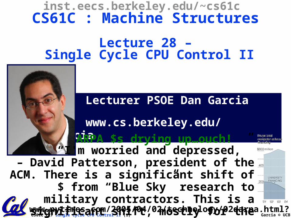
DARPA $s drying up…ouch!
www.nytimes.com/2005/04/02/technology/02darpa.html?
“I'm worried and depressed,” – David Patterson, president of the ACM.
There is a significant shift of $ from “Blue Sky” research to military contractors. This is a
significant shift, mostly for the worse.

CS61C L27 Single Cycle CPU Control II (2) Garcia © UCB
°5 steps to design a processor• 1. Analyze instruction set => datapath requirements• 2. Select set of datapath components & establish clock
methodology• 3. Assemble datapath meeting the requirements• 4. Analyze implementation of each instruction to
determine setting of control points that effects the register transfer.• 5. Assemble the control logic
°Control is the hard part°MIPS makes that easier• Instructions same size• Source registers always in same place• Immediates same size, location• Operations always on registers/immediates
Review: Single cycle datapath
Control
Datapath
Memory
ProcessorInput
Output

CS61C L27 Single Cycle CPU Control II (3) Garcia © UCB
A Summary of the Control Signals (2/2)
add sub ori lw sw beq jump
RegDst
ALUSrc
MemtoReg
RegWrite
MemWrite
nPCsel
Jump
ExtOp
ALUctr<2:0>
1
0
0
1
0
0
0
x
Add
1
0
0
1
0
0
0
x
Subtract
0
1
0
1
0
0
0
0
Or
0
1
1
1
0
0
0
1
Add
x
1
x
0
1
0
0
1
Add
x
0
x
0
0
1
0
x
Subtract
x
x
x
0
0
0
1
x
x
op target address
op rs rt rd shamt funct
061116212631
op rs rt immediate
R-type
I-type
J-type
add, sub
ori, lw, sw, beq
jump
func
op 00 0000 00 0000 00 1101 10 0011 10 1011 00 0100 00 0010Appendix A10 0000See 10 0010 We Don’t Care :-)

CS61C L27 Single Cycle CPU Control II (4) Garcia © UCB
32
ALUctr =
Clk
busW
RegWr =
3232
busA
32busB
55 5
Rw Ra Rb32 32-bitRegisters
Rs
Rt
Rt
RdRegDst =
Exten
der
Mu
x
Mux
3216imm16
ALUSrc =
ExtOp =
Mu
x
MemtoReg =
Clk
Data InWrEn
32Adr
DataMemory
32
MemWr =A
LU
InstructionFetch Unit
Clk
Zero
Instruction<31:0>
0
1
0
1
01<
21:25>
<16:20>
<11:15>
<0:15>
Imm16RdRsRt
• New PC = { PC[31..28], target address, 00 }
nPC_sel=
The Single Cycle Datapath during Jump
op target address02631
J-type jump25
Jump=
<0:25>
TA26

CS61C L27 Single Cycle CPU Control II (5) Garcia © UCB
The Single Cycle Datapath during Jump
32
ALUctr =x
Clk
busW
RegWr = 0
3232
busA
32busB
55 5
Rw Ra Rb32 32-bitRegisters
Rs
Rt
Rt
RdRegDst = x
Exten
der
Mu
x
Mux
3216imm16
ALUSrc = x
ExtOp = x
Mu
x
MemtoReg = x
Clk
Data InWrEn
32Adr
DataMemory
32
MemWr = 0A
LU
InstructionFetch Unit
Clk
Zero
Instruction<31:0>
0
1
0
1
01<
21:25>
<16:20>
<11:15>
<0:15>
RdRsRt
• New PC = { PC[31..28], target address, 00 }
nPC_sel=0
Jump=1
Imm16
<0:25>
TA26
op target address02631
J-type jump25

CS61C L27 Single Cycle CPU Control II (6) Garcia © UCB
Instruction Fetch Unit at the End of Jump
Adr
InstMemory
Ad
derA
dder
PC
Clk
00Mu
x
4
nPC_sel
imm
16
Instruction<31:0>
0
1
Zero
nPC_MUX_sel
• New PC = { PC[31..28], target address, 00 }op target address
02631J-type jump
25
How do we modify thisto account for jumps?
Jump

CS61C L27 Single Cycle CPU Control II (7) Garcia © UCB
Instruction Fetch Unit at the End of Jump
Adr
InstMemory
Ad
derA
dder
PC
Clk00
Mu
x
4
nPC_sel
imm
16
Instruction<31:0>
0
1
Zero
nPC_MUX_sel
• New PC = { PC[31..28], target address, 00 }op target address
02631J-type jump
25
Mu
x1
0
Jump
TA
26
4 (MSBs)
00
Query• Can Zero still get asserted?
• Does nPC_sel need to be 0? • If not, what?

CS61C L27 Single Cycle CPU Control II (8) Garcia © UCB
Build CL to implement Jump on paper now
Jump
Inst31Inst30Inst29Inst28Inst27Inst26Inst25
Inst01Inst00

CS61C L27 Single Cycle CPU Control II (11) Garcia © UCB
Review: Finite State Machine (FSM)
• States represent possible output values.
• Transitions represent changes between statesbased on inputs.
• Implement with CL andclocked registerfeedback.

CS61C L27 Single Cycle CPU Control II (12) Garcia © UCB
Finite State Machines extremely useful!
• They define •How output signals respond to input signals and previous state.
•How we change states depending on input signals and previous state
• The output signals could be our familiar control signals•Some control signals may only depend on CL, not on state at all…
• We could implement very detailed FSMs w/Programmable Logic Arrays

CS61C L27 Single Cycle CPU Control II (13) Garcia © UCB
Taking advantage of sum-of-products
• Since sum-of-products is a convenient notation and way to think about design, offer hardware building blocks that match that notation
• One example isProgrammable Logic Arrays (PLAs)
• Designed so that can select (program) ands, ors, complements after you get the chip• Late in design process, fix errors, figure out what to do later, …

CS61C L27 Single Cycle CPU Control II (14) Garcia © UCB
• • •
inputs
ANDarray
• • •
outputs
ORarrayproduct
terms
Programmable Logic Arrays
• Pre-fabricated building block of many AND/OR gates• “Programmed” or “Personalized" by making or
breaking connections among gates
• Programmable array block diagram for sum of products form
And Programming:• How many inputs?• How to combine inputs?• How many product terms?
Or Programming:• How to combine product terms?• How many outputs?

CS61C L27 Single Cycle CPU Control II (15) Garcia © UCB
example:
F0 = A + B' C'F1 = A C' + A BF2 = B' C' + A BF3 = B' C + A
personality matrix1 = uncomplemented in term0 = complemented in term– = does not participate
1 = term connected to output0 = no connection to output
input side: 3 inputs
output side: 4 outputsProduct inputs outputsterm A B C F0 F1 F2 F3
AB 1 1 – 0 1 1 0B'C – 0 1 0 0 0 1AC' 1 – 0 0 1 0 0B'C' – 0 0 1 0 1 0A 1 – – 1 0 0 1 reuse of terms;
5 product terms
Enabling Concept• Shared product terms among outputs

CS61C L27 Single Cycle CPU Control II (16) Garcia © UCB
Before Programming
• All possible connections available before “programming”

CS61C L27 Single Cycle CPU Control II (17) Garcia © UCB
A B C
F1 F2 F3F0
AB
B'C
AC'
B'C'
A
After Programming• Unwanted connections are "blown"
• Fuse (normally connected, break unwanted ones)
• Anti-fuse (normally disconnected, make wanted connections)

CS61C L27 Single Cycle CPU Control II (18) Garcia © UCB
notation for implementingF0 = A B + A' B'F1 = C D' + C' D
AB+A'B'CD'+C'D
AB
A'B'
CD'
C'D
A B C D
Alternate Representation
• Short-hand notation--don't have to draw all the wires• X Signifies a connection is present and
perpendicular signal is an input to gate

CS61C L27 Single Cycle CPU Control II (19) Garcia © UCB
Peer Instruction
A. MemToReg=‘x’ & ALUctr=‘sub’. SUB or BEQ?
B. ALUctr=‘add’. Which 1 signal is different for all 3 of: ADD, LW, & SW? RegDst or ExtOp?
C. “Don’t Care” signals are useful because we can simplify our PLA personality matrix. F / T?
ABC1: SRF2: SRT3: SEF4: SET5: BRF6: BRT7: BEF8: BET
32
ALUctr
Clk
busW
RegWr
3232
busA
32busB
55 5
Rw Ra Rb32 32-bitRegisters
Rs
Rt
Rt
Rd
RegDst
Exten
der
Mu
x
Mux
3216imm16
ALUSrc
ExtOp
Mu
x
MemtoReg
Clk
Data InWrEn
32Adr
DataMemory
32
MemWr
AL
U
InstructionFetch Unit
Clk
Zero
Instruction<31:0>
0
1
0
1
01
<21:25>
<16:20>
<11:15>
<0:15>
Imm16RdRsRt
nPC_sel

CS61C L27 Single Cycle CPU Control II (20) Garcia © UCB
°5 steps to design a processor• 1. Analyze instruction set => datapath requirements• 2. Select set of datapath components & establish clock
methodology• 3. Assemble datapath meeting the requirements• 4. Analyze implementation of each instruction to
determine setting of control points that effects the register transfer.• 5. Assemble the control logic
°Control is the hard part°MIPS makes that easier• Instructions same size• Source registers always in same place• Immediates same size, location• Operations always on registers/immediates
And in Conclusion… Single cycle control
Control
Datapath
Memory
ProcessorInput
Output