crest factor reduction application note - intel.com · 2 altera corporation preliminary crest...
TRANSCRIPT

Altera Corporation AN-396-1.0
June 2007, Version 1.0
Crest Factor Reduction
Application Note 396
This application note describes crest factor reduction and an Altera® crest factor reduction solution.
Overview A high peak-to-mean power ratio causes the following effects:
■ In-band distortion: ● High error vector magnitude (EVM) ● Degrades performance at receiver
■ Out-of-band distortion: ● Increased adajcent channel leakage ratio (ACLR) ● Degrades performance of users in adjacent channels
Figure 1 shows spectral regrowth with power amplifier (PA) distortion.
Figure 1. Spectral Regrowth with PA Distortion
0
Frequency
Spectral Regrowth
PA Ideal Response
PA DistortedNon-Linear Response
-10-20 10 20
1Preliminary

Crest Factor Reduction
Crest factor reduction (CFR) reduces the output peak-to-average ratio by clipping and allows additional gain on the output of CFR. You can operate closer to the amplifier compression point, therefore it is more efficient. Figure 2 shows output clipping with CFR.
Figure 2. Output Clipping with CFR
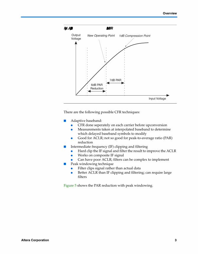
Figure 3 shows the amplifier transfer characteristics (before CFR); Figure 4 shows the amplifier transfer characteristics (after CFR).
Figure 3. Amplifier Transfer Characteristic—Before CFR
Time
Amplitude Clipped SignalClipping Threshold
Original Signalx(n)
Input Voltage
13dB PAR
OutputVoltage
Operating Point(Average)
1dB Compression Point
2 Altera CorporationPreliminary
Overview
Figure 4. Amplifier Transfer Characteristic—After CFR
There are the following possible CFR techniques:
■ Adaptive baseband: ● CFR done seperately on each carrier before upconversion ● Measurements taken at interpolated baseband to determine
which delayed baseband symbols to modify ● Good for ACLR; not so good for peak-to-average ratio (PAR)
reduction ■ Intermediate frequency (IF) clipping and filtering
● Hard clip the IF signal and filter the result to improve the ACLR ● Works on composite IF signal ● Can have poor ACLR; filters can be complex to implement
■ Peak windowing technique ● Filter clips signal rather than actual data ● Better ACLR than IF clipping and filtering; can require large
filters
Figure 5 shows the PAR reduction with peak windowing.
Input Voltage
7dB PAR
OutputVoltage
New Operating Point 1dB Compression Point
6dB PARReduction
Altera Corporation 3Preliminary
Crest Factor Reduction
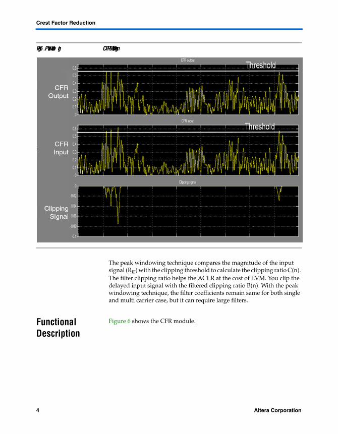
Figure 5. Peak Windowing CFR Block Diagram
The peak windowing technique compares the magnitude of the input signal (RIF) with the clipping threshold to calculate the clipping ratio C(n). The filter clipping ratio helps the ACLR at the cost of EVM. You clip the delayed input signal with the filtered clipping ratio B(n). With the peak windowing technique, the filter coefficients remain same for both single and multi carrier case, but it can require large filters.
Functional Description
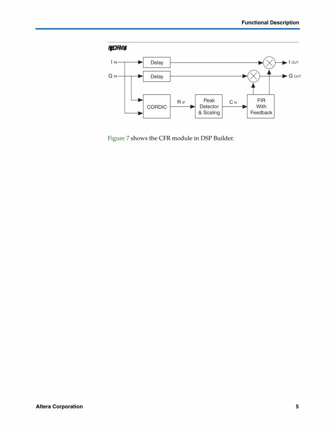
Figure 6 shows the CFR module.
4 Altera CorporationPreliminary
Functional Description
Figure 6. CFR Module
Figure 7 shows the CFR module in DSP Builder.
FIRWith
Feedback
PeakDetector& Scaling
CORDIC
I IN
R IF C N
Q IN
I OUT
Q OUTDelay
Delay
Altera Corporation 5Preliminary
Crest Factor Reduction
Figure 7. CFR Module in DSP Builder
6 Altera CorporationPreliminary
Functional Description
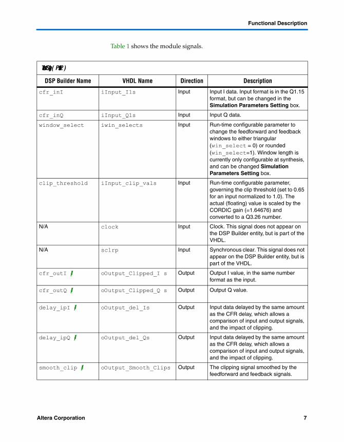
Table 1 shows the module signals.
Table 1. Signals (Part 1 of 2)
DSP Builder Name VHDL Name Direction Description
cfr_inI iInput_I1s Input Input I data. Input format is in the Q1.15 format, but can be changed in the Simulation Parameters Setting box.
cfr_inQ iInput_Q1s Input Input Q data.
window_select iwin_selects Input Run-time configurable parameter to change the feedforward and feedback windows to either triangular (win_select = 0) or rounded (win_select=1). Window length is currently only configurable at synthesis, and can be changed Simulation Parameters Setting box.
clip_threshold iInput_clip_vals Input Run-time configurable parameter, governing the clip threshold (set to 0.65 for an input normalized to 1.0). The actual (floating) value is scaled by the CORDIC gain (=1.64676) and converted to a Q3.26 number.
N/A clock Input Clock. This signal does not appear on the DSP Builder entity, but is part of the VHDL.
N/A sclrp Input Synchronous clear. This signal does not appear on the DSP Builder entity, but is part of the VHDL.
cfr_outI (1) oOutput_Clipped_I s Output Output I value, in the same number format as the input.
cfr_outQ (1) oOutput_Clipped_Q s Output Output Q value.
delay_ipI (1) oOutput_del_Is Output Input data delayed by the same amount as the CFR delay, which allows a comparison of input and output signals, and the impact of clipping.
delay_ipQ (1) oOutput_del_Qs Output Input data delayed by the same amount as the CFR delay, which allows a comparison of input and output signals, and the impact of clipping.
smooth_clip (1) oOutput_Smooth_Clips Output The clipping signal smoothed by the feedforward and feedback signals.
Altera Corporation 7Preliminary

Crest Factor Reduction
Getting Started This section involves the following steps:
■ “Software Requirements” on page 8■ “Simulink Simulation” on page 8■ “Autogenerate RTL” on page 20■ “Synthesize the Design” on page 20■ “Perform RTL Simulation” on page 21■ “Verify Simulink Model & RTL” on page 25
Software Requirements
This application note requires the following software:
■ MATLAB version release 14■ Simulink version 6 ■ DSP Builder version 7.1 ■ The Quartus® II software version 7.1 ■ The ModelSim® simulation tool version 5.7d
Simulink Simulation
To simulate in Simulink, follow these steps:
■ “Set Up” on page 9■ “Parameterize the Design” on page 9
raw_clip (1) oOutput_raw_clips Output The raw clipping signal. The positive part of the input minus the clipping threshold.
raw_FIR_ip (1) oOutput_raw_FIR_ips Output The input to the feedforward filter (equal to the raw clipping signal minus the feedback filter).
FIR_ip (1) oOutput_mFIR_ips Output The input to the feedforward filter (equal to the raw clipping signal minus the feedback filter) but with any negative values set to zero.
feedb_FIR_op (1) oOutput_fFIR_ops Output The output of the feedback FIR, which reduces any overclipping caused by adjacent, high-clipping values.
Note to Table 1:(1) Debug outputs, which are included for testing only, and if unconnected the Quartus II software synthesizes away any associated
logic.
Table 1. Signals (Part 2 of 2)
DSP Builder Name VHDL Name Direction Description
8 Altera CorporationPreliminary
Getting Started
■ “Run the Simulation” on page 17
Set Up
To simulate in Simulink, follow these steps:
1. Open the MATLAB software.
2. Include additional paths:
a. Go to the top-level directory <install directory>\altera_wireless.
b. Type add_wireless_paths.
Parameterize the Design
You can either use the two testbenches included with the reference design or instantiate the CFR in a new design (see “Instantiate the CFR Module in a New Design” on page 15). The two testbenches include an instantiated and parameterized CFR module, which you can use to explore the design.
TestbenchesAltera provide the following two testbenches:
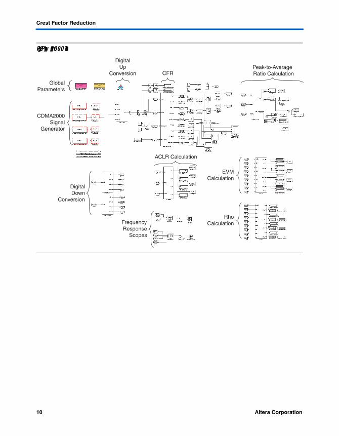
■ Peak_win_cdma2000 (see Figure 8). The CDMA2000 source within testbench generates input data.
■ Peak_win_wkspace (see Figure 9). Input data is read from the workspace. A sample input file is included in the ip_data directory. This file (FA4_CDMA2000) is for CDMA2000 with four carriers. The file length is 5 ms for an input data rate of 78.6 MHz (CDMA2000 rate upsampled by 64). With a pre-generated workspace variable as an input, the simulation time is shorter.
Altera Corporation 9Preliminary
Crest Factor Reduction
Figure 8. Peak_win_cdma2000 Testbench
EVM Calculation
Rho Calculation Frequency
Response Scopes
Digital Down
Conversion
CDMA2000 Signal
Generator
GlobalParameters
CFR
Digital Up
Conversion Peak-to-Average Ratio Calculation
ACLR Calculation
10 Altera CorporationPreliminary

Getting Started
Figure 9. Peak_win_wkspace Testbench
v Open the model by typing open_cfr. This script performs the following actions:
● Changes the directory to <install directory>\altera_wireless\ip\cfr\test\matlab.
● Opens the peak_win_cdma2000.mdl testbench. ● Updates the model to include the currently defined settings.
1 If you change the settings, or open a model directly in Simulink, you must update the model to reflect the variable settings:
1 Alternatively, open testbench peak_win_wkspace from the same location.
To parameterize the design double-click the global configuration parameter box on the top left of the design. Figure 10 shows the Simulation Parameter Settings.
EVMMeasurement
FrequencyDomain
Scope
Input fromWorkspace
CFRPeak-to-Average Ratio Calculation
ACLR Measurement
Altera Corporation 11Preliminary

Crest Factor Reduction
Figure 10. Simulation Parameter Settings
12 Altera CorporationPreliminary

Getting Started
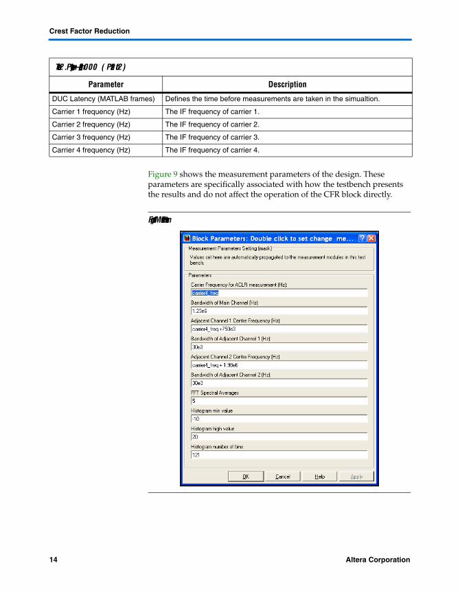
Table 4 shows the parameters for peak_win_cdma2000.
1 The peak_win_wkspace testbench uses a subset of these parameters.
Table 2. Parameters—peak_win_cdma2000 (Part 1 of 2)
Parameter Description
Cliping Amplitude (CFR block) The value at which the clipping occurs, in floating point.
IO Signed Fractional: [number of bit].[]
The number of integer bits in the input data and data path in the design. For example, for one 16-bit signed number less than 1.0 (i.e. Q1.15), this is set as 1
IO Signed Fractional: [].[number of bit]
The number of fractional bits in the input data and data path in the design. For example, for one 16-bit signed number less than 1.0 (Q1.15), this is set as 15.
Clip Value Signed Fractional: [2].[number of bit]
The number of fractional bits for the clipping calculation in the design. Two magnitude and sign bits are used by default (the number is 2.0 > value ≥ –2.0).
Typically this number can be less than the input bit width, to reduce complexity. For example, 11 bits can be used here, making the overall number format Q2.11.
Peak Window Length The width of the feed-forward filter impulse response, in samples. The feedback filter impulse response is one-half of this value.
Chip Rate CDMA2000 chip rate (default setting is 1.2288 MHz).
CDMA2000 Frame length (seconds)
CDMA2000 frame length (default setting is 2,048 chips).
BS Tx MATLAB Frame Length (number of chips)
Processing interval size for the MATLAB/Simulink simulation (default setting is 2,048 chips).
Carrier 1 Random Generator Seed
The random seed from the CDMA2000 signal source.
Carrier 2 Random Generator Seed
Carrier 3 Random Generator Seed
Carrier 4 Random Generator Seed
Pulse Shaper Group Delay (number of samples)
Latency associated with the root-raised cosine filter that pulse shapes the transmitted signal (default value is 24).
Pulse Shaper Interpolation Factor Interpolation rate for pulse shaping filter (default value is 4, corresponding to 4 × 1.2288 MHz = 4.91 MHz).
DUC Interpolation Factor Digital upconversion interpolation factor (default value is 16, corresponding to 16 × 4.91 MHz = 78.64 MHz).
CFR Latency (MATLAB frames) Defines the time before measurements are taken in the simualtion.
Altera Corporation 13Preliminary
Crest Factor Reduction
Figure 9 shows the measurement parameters of the design. These parameters are specifically associated with how the testbench presents the results and do not affect the operation of the CFR block directly.
Figure 11. Measurement Parameters
DUC Latency (MATLAB frames) Defines the time before measurements are taken in the simualtion.
Carrier 1 frequency (Hz) The IF frequency of carrier 1.
Carrier 2 frequency (Hz) The IF frequency of carrier 2.
Carrier 3 frequency (Hz) The IF frequency of carrier 3.
Carrier 4 frequency (Hz) The IF frequency of carrier 4.
Table 2. Parameters—peak_win_cdma2000 (Part 2 of 2)
Parameter Description
14 Altera CorporationPreliminary

Getting Started
Table 4 shows the measurement parameters.
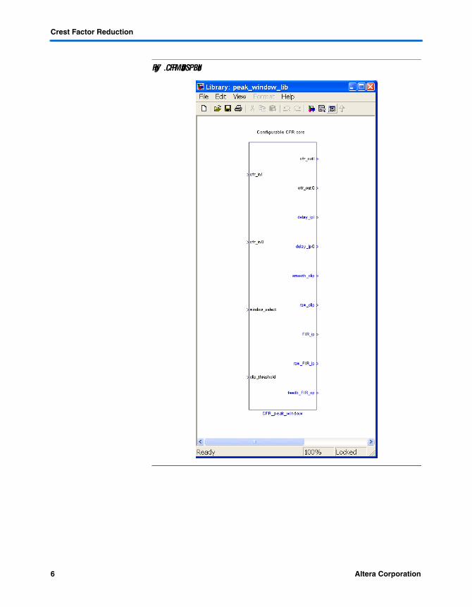
Instantiate the CFR Module in a New DesignTo instantiate the CFR module in a new design from the Simulink library, follow these steps:
1. Open the MATLAB and Simulink software.
2. Open the Altera Wireless Library.
3. Open the Radio Card Library.
4. Open the Crest Factor Reduction Library.
5. Open the Peak Windowing Library.
6. Drag the CFR_peak_window module into the Simulink project.
To choose the parameters, double click on the CFR block (see Figure 12).
Table 3. Measurement Parameters
Parameter Description
Carrier Frequency for ACLR measurement (Hz)
Centre frequency of desired channel for ACLR measurement.
Bandwidth of Main Channel (Hz)
Bandwidth over which to taken the power measurement for the desired channel.
Adjacent Channel 1 Centre Frequency (Hz)
Centre frequency of the first unwanted interferer for ACLR measurement.
Bandwidth of Adjacent Channel 1 Channel (Hz)
Bandwidth over which to take the power measurement for the first unwanted interferer.
Adjacent Channel 2 Centre Frequency (Hz)
Centre frequency of the second unwanted interferer for ACLR measurement.
Bandwidth of Adjacent Channel 2 Channel (Hz)
Bandwidth over which to take the power measurement for the second unwanted interferer.
FFT Spectral Averages The number of frames of data that are combined for a single plot of the output spectrum. Low numbers cause the scope to update faster but with a less accurate measurement.
Histogram min value The lowest value for the peak-to-average ratio PDF calculation (dB).
Histogram max value The highest value for the peak-to-average ratio PDF calculation (dB).
Histogram number of bins
The number of bins in the the peak-to-average ratio PDF calculation. For example, when set to 121 with a maximum value of 20dB and a minimum of –10 dB, the resolution is given by:
(20 – (–10))/(121 – 1) = 0.25dB
Altera Corporation 15Preliminary

Crest Factor Reduction
Figure 12. Parameters
Table 4 shows the CFR module parameters.
Table 4. Parameters (Part 1 of 2)
Parameter Description
Clip threshold value (amplitude)
The value at which the clipping occurs.
Sample time The sampling interval at CFR input.
16 Altera CorporationPreliminary

Getting Started
Run the Simulation
To run the simulation, choose Start (Simulation menu).
Simulation Visualization
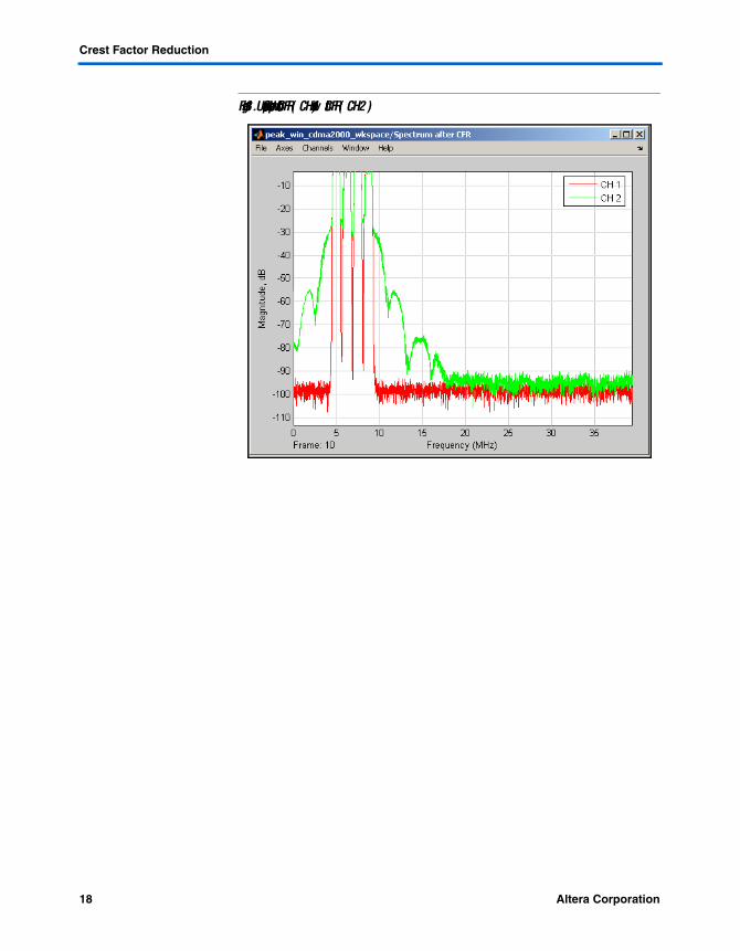
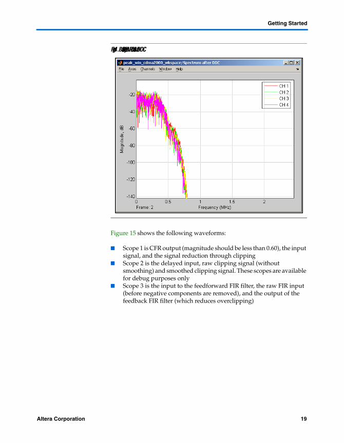
Figures 13 and 14 show the frequency spectrum after CFR and after digital downconversion, which shows the spectral leakage into the adjacent channels.
1 For the testbenches, Altera provides several measurement blocks.
IO signed fractional: [number of bits].[]
The number of integer bits in the input data and datapath in the design. For example, for one 16-bit signed number less than 1.0 (Q1.15), set to 1.
IO signed fractional: [].[number of bit]s
The number of fractional bits in the input data and datapath in the design. For example, for one 16 bit signed number less than 1.0 (Q1.15), set to15.
Clip Value Signed Fractional: [2].[number of bit]
The number of fractional bits used for the clipping calculation in the design. Two magnoitude and sign bits are used by default (the number is 2.0 >value> = –2.0). Typically this value can be less than the input bit width, to reduce complexity. For example, for 11 bits the overall number format is Q2.11.
Peak Window Length The width of the feed-forward filter impulse response, in samples.The feedback filter impulse response is one-half of this value.
Scale Compensation factor Scaling for peak window calculation.
CORDIC phase bit width The size of the calculation for phase in CORDIC.
CORDIC XY precision The increase in the resolution in the CORDIC magnitude calculation.
CORDIC Z precision bits The increase in the reolution of the phase calculation in the CORDIC (not required).
Table 4. Parameters (Part 2 of 2)
Parameter Description
Altera Corporation 17Preliminary
Crest Factor Reduction
Figure 13. Upconverted Spectrum Without CFR (CH1) and with CFR (CH2)
18 Altera CorporationPreliminary
Getting Started
Figure 14. Baseband Spectrum For All Four Carriers After DDC
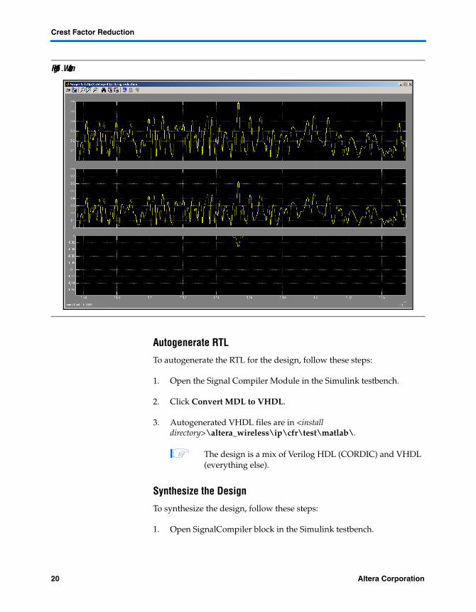
Figure 15 shows the following waveforms:
■ Scope 1 is CFR output (magnitude should be less than 0.60), the input signal, and the signal reduction through clipping
■ Scope 2 is the delayed input, raw clipping signal (without smoothing) and smoothed clipping signal. These scopes are available for debug purposes only
■ Scope 3 is the input to the feedforward FIR filter, the raw FIR input (before negative components are removed), and the output of the feedback FIR filter (which reduces overclipping)
Altera Corporation 19Preliminary
Crest Factor Reduction
Figure 15. Waveforms
Autogenerate RTL
To autogenerate the RTL for the design, follow these steps:
1. Open the Signal Compiler Module in the Simulink testbench.
2. Click Convert MDL to VHDL.
3. Autogenerated VHDL files are in <install directory>\altera_wireless\ip\cfr\test\matlab\.
1 The design is a mix of Verilog HDL (CORDIC) and VHDL (everything else).
Synthesize the Design
To synthesize the design, follow these steps:
1. Open SignalCompiler block in the Simulink testbench.
20 Altera CorporationPreliminary

Getting Started
1. Click Execute steps 1, 2 and 3 to autogenerate RTL, and perform synthesis and fitting.
To modify the synthesis and fitting settings, follow these steps:
1. Change to the <install dir>\altera_wireless\ip\cfr\test\matlab\ directory.
2. Open the Quartus II software.
3. Open the DSP Builder-generated Quartus II project with the same name as the Simulink model file.
4. Configure the constraints on the design and select the device type (if different from default).
5. Choose Start Compilation (Processing menu).
Perform RTL Simulation
To perform RTL simulation, follow these steps:
6. Open the SignalCompiler block in the Simulink testbench
7. Click the Testbench tab.
8. Turn on Generate stimuli for VHDL testbench.
9. Click OK.
10. In Simulink choose Start (Simulation menu). Input data is logged to files <install dir>\altera_wireless\ip\cfr\test\matlab\DSP Builder_<Simulink model name>\<signal name>.salt.
When generating VHDL, DSP Builder also generates a testbench <install dir>\altera_wireless\ip\cfr\test\matlab\tb_<Simulink model name>.vhd.
11. Open tb_<Simulink model name>.tcl.
12. Replace the following code:
puts "################################################################################################################# "puts "# "puts "# DSP Builder INFORMATION :"
Altera Corporation 21Preliminary
Crest Factor Reduction
puts "# The entity Cordic_subsystem is a DSP Builder subsystem black-box"puts "# Prior to simulate the design, make sure to compile in ModelSim all the HDL files used for the black box subsystem Cordic_subsystem"puts "# "puts "################################################################################################################# "
with the following code:
set cordicdir "../../../../../cordic/source/verilog"vlog +incdir+$cordicdir -y $cordicdir +libext+.v "Cordic_subsystem.v"
13. Start the ModelSim simulator.
14. Choose Execute Macro and choose the following Tcl script to run <install dir>\altera_wireless\ip\cfr\test\matlab\<Simulink model name>.tcl.
This script compiles all the relevant design files and runs the testbench. The testbench reads the input data generated by Simulink and feeds this into the RTL. The VHDL testbench writes all signals that were defined as outputs in the Simulink design to text files.
22 Altera CorporationPreliminary

Performance
Performance Resource usage depends on window length and window type (rounded or triangular). Table 5 and Table 6 show performance for triangular window, length 64.
Table 7 and Table 8 show performance for rounded window, length 64..
Appendix A: Results
This appendix list results for W-CDMA and CDMA-2000.
Table 5. Performance—Triangular Window, Length 64
Device LEs 9 × 9 Multipliers
Memory fMAX (MHz)Bits M4K M9K
Cyclone 3754 0 36580 6 – 94
Cyclone II 2823 12 3658 6 – 94
Cyclone III 2801 12 3658 – 6 95
Table 6. Performance—Triangular Window, Length 64
Device Combinational ALUTs
Logic Registers
18 × 18 Multipliers
MemoryfMAX (MHz)
Bits M4K M9K M512
Stratix II 1922 1867 20 3658 2 – 4 111
Stratix III 1922 1867 24 3658 – 6 – 111
Table 7. Performance—Rounded Window, Length 64
Device LEs 9 × 9 Multipliers
Memory fMAX (MHz)Bits M4K M9K
Cyclone II 2879 12 3664 8 – 100
Cyclone III 2880 12 3664 – 8 107
Table 8. Performance—Rounded Window, Length 64
Device Combinational ALUTs
Logic Registers
18 × 18 Multipliers
MemoryfMAX (MHz)
Bits M4K M9K M512
Stratix II 2008 1953 20 3664 2 – 6 115
Stratix III 2008 1953 24 3664 – 8 – 114
Altera Corporation 23Preliminary

Crest Factor Reduction
W-CDMA
Figures 16 and 17 show the performance for W-CDMA, with three carriers for test case 1. The results have the following conditions:
■ EVM = 13.8%■ Output PAR = 6.5dB ■ PAR reduction = 4dB at probably 10-4
Figure 16. Complementary Cumulative Density Function (CCDF)
24 Altera CorporationPreliminary

Appendix A: Results
Figure 17. Spectral Leakage with CFR
CDMA-2000
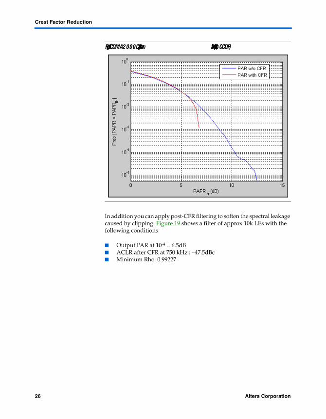
Figure 18 shows indicative performance for CDMA2000, for four carriers, with the following conditions:
■ Output PAR at 10-4 = 6.7dB ■ ACLR after CFR at 750 kHz: –46.0dBc ■ 3GPP2 spec: –45dBc ■ Channel quality (Rho): 0.9951 ■ 3GPP2 spec: > 0.985
Altera Corporation 25Preliminary
Crest Factor Reduction
Figure 18. CDMA2000 Complementary Cumulative Density Function (CCDF)
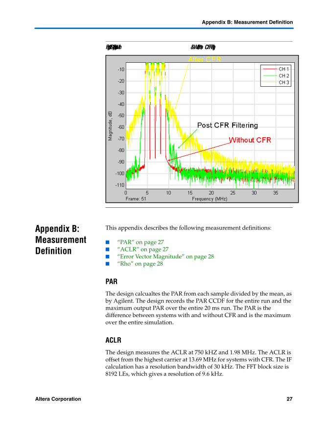
In addition you can apply post-CFR filtering to soften the spectral leakage caused by clipping. Figure 19 shows a filter of approx 10k LEs with the following conditions:
■ Output PAR at 10-4 = 6.5dB ■ ACLR after CFR at 750 kHz : –47.5dBc ■ Minimum Rho: 0.99227
26 Altera CorporationPreliminary
Appendix B: Measurement Definition
Figure 19. Spectral Response With & Without Post-CFR Filtering
Appendix B: Measurement Definition
This appendix describes the following measurement definitions:
■ “PAR” on page 27■ “ACLR” on page 27■ “Error Vector Magnitude” on page 28■ “Rho” on page 28
PAR
The design calcualtes the PAR from each sample divided by the mean, as by Agilent. The design records the PAR CCDF for the entire run and the maximum output PAR over the entire 20 ms run. The PAR is the difference between systems with and without CFR and is the maximum over the entire simulation.
ACLR
The design measures the ACLR at 750 kHZ and 1.98 MHz. The ACLR is offset from the highest carrier at 13.69 MHz for systems with CFR. The IF calculation has a resolution bandwidth of 30 kHz. The FFT block size is 8192 LEs, which gives a resolution of 9.6 kHz.
Altera Corporation 27Preliminary

Crest Factor Reduction
Error Vector Magnitude
The design calculates the error vector magnitude every slot and records the maximum for the entire run.
Rho
The 3GPP2 specification gives the following definition for rho:
■ Zk is the kth sample of the output of the complementary filter ■ R0,k is the corresponding sample of the ideal output of the
complementary filter.
28 Altera CorporationPreliminary
101 Innovation DriveSan Jose, CA 95134www.altera.com
Copyright © 2007 Altera Corporation. All rights reserved. Altera, The Programmable Solutions Company,the stylized Altera logo, specific device designations, and all other words and logos that are identified astrademarks and/or service marks are, unless noted otherwise, the trademarks and service marks of AlteraCorporation in the U.S. and other countries. All other product or service names are the property of their re-spective holders. Altera products are protected under numerous U.S. and foreign patents and pendingapplications, maskwork rights, and copyrights. Altera warrants performance of its semiconductor productsto current specifications in accordance with Altera's standard warranty, but reserves the right to make chang-es to any products and services at any time without notice. Altera assumes no responsibility or liabilityarising out of the application or use of any information, product, or service describedherein except as expressly agreed to in writing by Altera Corporation. Altera customersare advised to obtain the latest version of device specifications before relying on any pub-lished information and before placing orders for products or services.