crd44600-ph-fb stereo 100 w pwm amplifier reference design · crd44600-ph-fb 4 mar '05...
TRANSCRIPT

Copyright © Cirrus Logic,(All Rights Reserv
Cirrus Logic, Inc.www.cirrus.com
CRD44600-PH-FB
Stereo 100 W PWM Amplifier Reference Design
FeaturesTwo full-bridge channels, 100 W each106 dB Dynamic Range - both channels0.015% THD+N at 1 WPower Supply Rejection (PSR) feedback allowing amplifier to operate from low cost linear unregulated power supplies
Spread Spectrum Modulation - Reduces Modulation Energy
Passes CISPR and FCC requirements for radiated and power line conducted emissions
Independent peak signal limiting per channelThermal and over-current protection> 85% amplifier efficiencyWorks with GUI to configure the boardDemonstrates recommended layout and grounding arrangements
DescriptionThe CRD44600-PH-FB PWM Amplifier demonstratesthe CS44600, Cirrus’ multi-channel pure digital PWM
controller. This reference design implements a two-channel amplifier which delivers 100 W per full-bridgechannel into 8 Ω loads using a single +50 V supply (at1% THD+N). A 155 W unregulated linear power supplyis used to power the CRD44600-PH-FB.
As shown below, the CS44600 IC takes two stereo digi-tal audio PCM inputs and converts them to PWMoutputs. This 64-pin LQFP PWM controller provides anintegrated sample rate converter for 32 kHz-192 kHz in-put sample rate support, volume up/down, speaker loadcompensation, peak limiting to prevent amplifier clipping,power supply ripple compensation, and AM frequencyinterference elimination.
This reference design uses the the Philips TDA8939, anintegrated power stage back end for digital amplifiers(two TDA8939 parts configured as full-bridges are usedfor this two-channel design). Current limiting and ther-mal protection are provided by the TDA8939.
The inductor/capacitor 2nd order low pass filter (LPF) re-moves high frequency components from the outputsignal effectively converting it from digital to analog.
ORDERING INFORMATIONCRD44600-PH-FB Reference Design
I
PhilipsTDA8939
CS44600(PWM Controller)
LPFChannel 1
+50 V
CS4461 ADC
+50 VPSR Circuitry
Audio Inputs and GUIInterface
155W UnregulatedLinear Power Supply
PhilipsTDA8939 LPF
+50 V
Channel 2
+50 V
PCM Clocks & Data
I2C Host Control
8 Ω
8 Ω
1
Inc. 2005ed) MAR '05
DS633RD1

CRD44600-PH-FB
TABLE OF CONTENTS1. SYSTEM OVERVIEW ............................................................................................................... 3
1.1 CS44600 PWM Modulator ................................................................................................. 31.2 CS4461 PSR Feedback ADC ............................................................................................ 31.3 TDA8939 Power Stage ...................................................................................................... 31.4 CS8416 Digital Audio Receiver .......................................................................................... 31.5 CS5341 Analog to Digital Converter .................................................................................. 31.6 Control Port Interface and GUI .......................................................................................... 41.7 Unregulated Linear Power Supply ..................................................................................... 4
2. GUI CONTROL ......................................................................................................................... 52.1 CS44600 Dialog Tab .......................................................................................................... 52.2 Advanced Register Debug Tab .......................................................................................... 6
3. POWER SUPPLY ..................................................................................................................... 83.1 Power Supply Ratings ........................................................................................................ 83.2 Power Supply Decoupling .................................................................................................. 8
4. ELECTROMAGNETIC INTERFERENCE (EMI) ....................................................................... 94.1 Suppression of EMI at the Source ..................................................................................... 94.2 EMI Testing ........................................................................................................................ 9
5. CRD44600-PH-FB SCHEMATICS ......................................................................................... 146. CRD44600-PH-FB POWER SUPPLY SCHEMATICS ........................................................... 197. CRD44600-PH-FB LAYOUT ................................................................................................... 208. CRD44600-PH-FB BILL OF MATERIALS ....................................................................... 239. TYPICAL PERFORMANCE PLOTS ....................................................................................... 2510. REVISION HISTORY ............................................................................................................ 30
LIST OF FIGURESFigure 1. CS44600 Dialog Tab........................................................................................................ 5Figure 2. Advanced Register Debug Tab - CS44600...................................................................... 6Figure 3. Advanced Register Debug Tab - CS8416........................................................................ 7Figure 4. EMI Testing Setup.......................................................................................................... 11Figure 5. EMI Testing Setup, Close-up ......................................................................................... 11Figure 6. Radiated EMI Testing Results- 30 MHz to 200 MHz...................................................... 12Figure 7. Radiated EMI Testing Results- 200 MHz to 1 GHz........................................................ 12Figure 8. Conducted Power Line Testing Results ......................................................................... 13Figure 9. Audio Inputs ................................................................................................................... 14Figure 10. CS44600 ...................................................................................................................... 15Figure 11. PSR Feedback ............................................................................................................. 16Figure 12. Left/Right Channels...................................................................................................... 17Figure 13. Control Port and Power................................................................................................ 18Figure 14. Power Supply ............................................................................................................... 19Figure 15. Silk Screen Top............................................................................................................ 20Figure 16. Topside Layer .............................................................................................................. 21Figure 17. Bottomside Layer ......................................................................................................... 22Figure 18. Frequency Response ................................................................................................... 25Figure 19. THD+N vs. Frequency at 1 W, 10 W, and 50 W .......................................................... 26Figure 20. THD+N vs. Power at 1 kHz .......................................................................................... 27Figure 21. FFT at -60 dBFS and 1 kHz ......................................................................................... 28Figure 22. FFT at -1 dBFS and 1 kHz. Red = PSR Feedback Off. Blue = PSR Feedback On ..... 29
LIST OF TABLES
2 MAR '05 DS633RD1

CRD44600-PH-FB
Table 1. Bill of Materials................................................................................................................ 23Table 2. Revision History .............................................................................................................. 30
MAR '05 DS633RD1 3
CRD44600-PH-FB
1. SYSTEM OVERVIEW The CRD44600-PH-FB reference design is an excellent means for evaluating the CS44600 six-channel Class-D PWM modulator. It incorporates a digital Class-D PWM modulator, two full-bridge power stages, and power supply rejection (PSR) circuitry, all on a two-layer board.
The CRD44600-PH-FB schematic set is shown in Figures 9 through 13 and the board layout isshown in Figures 15 through 17.
1.1 CS44600 PWM ModulatorA complete description of the CS44600 is included in the CS44600 product data sheet.
The CS44600 converts linear PCM data to pulse width modulated (PWM) output. It uses aSample Rate Converter (SRC) to eliminate serial audio interface jitter effects and maintainsa constant PWM switch rate of 384 kHz, resulting in high-quality sound output.
PCM data and clocks are input from either the CS8416 (S/PDIF Receiver), CS5341 (StereoADC), or J19 (PCM Input Header).
1.2 CS4461 PSR Feedback ADCA complete description of the CS4461 is included in the CS4461 product data sheet.
The CS4461 is connected to the CS44600 to provide power supply rejection (PSR) for theVP supply voltage connected to J17. Resistors R41 and R42 are set for VP = +50 V. See theCS4461 data sheet for equations to determine the resistor values.
1.3 TDA8939 Power StageA complete description of the Philips TDA8939 is included in the TDA8939 product datasheet.
The TDA8939 is a high-voltage PWM amplifier power stage. It integrates two half-bridge driv-ers and fault protection. For the CRD44600-PH-FB, each of the two TDA8939’s are config-ured as full-bridges. Care should be taken to not connect the full bridge black speakerconnectors to ground as these outputs are driven.
1.4 CS8416 Digital Audio ReceiverThe operation of the CS8416 receiver and a discussion of the digital audio interface are de-scribed in the CS8416 data sheet.
The CS8416 converts the input S/PDIF data stream into PCM data for the CS44600. TheCS8416 operates in master mode with RMCK = 256*Fs. The digital Interface format is set toLeft Justified (24-bit).
D20 (RERR) indicates a receiver error, such as loss of lock.
S/PDIF input is through OPT1 or J33.
1.5 CS5341 Analog to Digital ConverterThe operation of the CS5341 ADC is described in the CS5341 data sheet.
4 MAR '05 DS633RD1
CRD44600-PH-FB
The CS5341 converts analog audio into PCM data for the CS44600. The CS5341 operatesin slave mode and the digital Interface format is set to Left Justified (24-bit).
Analog input is through J5 and J6.
1.6 Control Port Interface and GUIThe CS44600 and CS8416 are controlled through the provided control port interface. Con-nection to the control port is made through J37 (RS-232 Serial). A Windows based GUI pro-vides control over all the individual registers of the CS44600 and the CS8416.
1.7 Unregulated Linear Power SupplyThe power supply used for the CRD44600-PH-FB is a linear 155 W supply. The supply pro-vides an unregulated +50 V for the TDA8939 power stages. The power supply consists of atransformer, diode bridge rectifier, and bulk capacitor. Schematics are shown in Figure 14.
MAR '05 DS633RD1 5

CRD44600-PH-FB
2. GUI CONTROLThe CRD44600-PH-FB is shipped with a Microsoft Windows® based GUI, which allows controlover the CS8416 and CS44600 registers. Interface to the CDB44600 control port is provided us-ing an RS-232 serial cable. The GUI requires no installation and can be run directly from the CDor copied to a local directory and run from there. Once the serial port cable is connected betweenthe CRD44600-PH-FB and the host PC, load the FlexLoader.exe from the CRD44600-PH-FB di-rectory. Once loaded, all registers are set to their default reset state. The GUI File menu pro-vides the ability to save and restore (load) register settings. Sample script files are provided forbasic functionality. The GUI serial port interface is setup by default for 115.2 Kbps operation onCOM1. To change these settings, edit the “CRD44600-PH-FBCommunications” section of theflexconfig.ini file or change the system communications setting in the Windows® control panel.
2.1 CS44600 Dialog TabThe CS44600 Dialog tab provides high level control over the CS44600’s registers. Controlsare provided to change volume, mute, enable PSR, enable the power stages, limiter control.
Figure 1. CS44600 Dialog Tab
6 MAR '05 DS633RD1
CRD44600-PH-FB
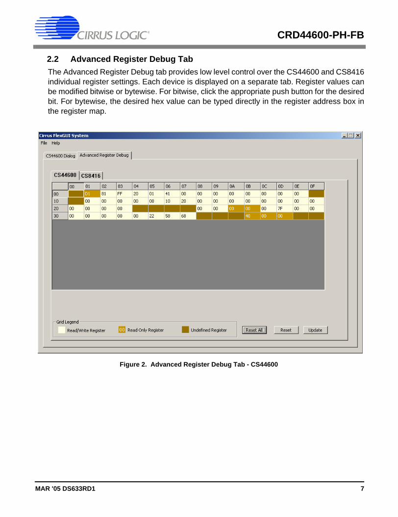
2.2 Advanced Register Debug TabThe Advanced Register Debug tab provides low level control over the CS44600 and CS8416individual register settings. Each device is displayed on a separate tab. Register values canbe modified bitwise or bytewise. For bitwise, click the appropriate push button for the desiredbit. For bytewise, the desired hex value can be typed directly in the register address box inthe register map.
Figure 2. Advanced Register Debug Tab - CS44600
MAR '05 DS633RD1 7

CRD44600-PH-FB
Figure 3. Advanced Register Debug Tab - CS8416
8 MAR '05 DS633RD1

CRD44600-PH-FB
3. POWER SUPPLY
3.1 Power Supply RatingsThe required power supply current rating can be estimated as follows. 95 W is used as thereference output power per channel because this represents the typical full scale output withno clipping. Assume the efficiency, η, is approximately 85% (this accounts for power to sup-ply control electronics and overhead), then for 95 W x 2 channels:
Consequently the supply current is:
The factor of 2 in the denominator of the PSupply calculation arises from the fact that for typicalconsumer applications in A/V or DVD receivers, the power supply should be capable of pro-viding ½ the total requirement for all channels operating at full power. This design guide isstill quite conservative, and gives more than adequate headroom in real applications.
3.2 Power Supply DecouplingProper power supply decoupling is one key to maximizing the performance of a Class-D am-plifier. Because the design uses an open loop output stage, noise on the power supply railwill be coupled to the output. While the PSR functionality of the CS44600 helps reduce powersupply noise feedthrough to the output, careful decoupling of the power stage supply rails isessential. Referring to Figure 15, the top side of the CRD44600-PH-FB PWM amplifier board,good decoupling practice is shown. Notice that the 0.1 µF ceramic capacitors are as closeas physically possible to the power pins of the TDA8939. The ground side of the capacitorsis connected directly to top side ground plane, which is also used by the power supply returnpins. This keeps the high frequency current loop small to minimize power supply variationsand EMI. 470 µF electrolytic capacitors are also located in close proximity to the power sup-ply pins to supply the current locally for each channel. These are not required to be expensivelow ESR capacitors. General purpose electrolytic capacitors that are specified to handle theripple current can be used. The real time PSR feedback of the CS44600/CS4461 can greatlyattenuate the induced voltages due to the power supply ripple current.
WWPP OutTotal 224
85.0190 ===
η
WWPP TotalSupply 112
2224
2===
AVW
VPI
Supply
SupplySupply 24.2
50112 ===
MAR '05 DS633RD1 9
CRD44600-PH-FB
4. ELECTROMAGNETIC INTERFERENCE (EMI)This reference design from Cirrus Logic is a board level solution which is meant to controlemissions by minimizing and suppressing them at the source in contrast to containing themin an enclosure. Utilizing spread spectrum modulation techniques to reduce the overallswitching energy, along with a low internal modulator clock frequency of 24.576 MHz, the ra-diated emissions are greatly reduced. These features allow for the use of very low cost com-ponents to couple the high frequency noise to chassis ground. No common mode chokes,inductors, or power line filters were required.
The EMI requirements for an amplifier have added dimensions beyond those imposed onpower supplies. Audio amplifiers are usually located in close proximity to radio receivers, par-ticularly AM receivers which are notoriously sensitive to interference. Amplifiers also need tooperate with speaker leads of unpredictable length and construction which make it possiblefor any high frequency currents that appear on the outputs to generate nuisance emissions.
4.1 Suppression of EMI at the SourceSeveral techniques are used in the circuit design and board layout to minimize high fre-quency fields in the immediate vicinity of the high power components. Specific techniquesinclude the following:
• As was mentioned in Section 3.2, effective power supply decoupling of high frequency cur-rents, and minimizing the loop area of the decoupling loop is one aspect of minimizing EMI.
• Each output of the TDA8939 includes “snubbing” components. For example, OUT1 of U1 in-cludes snubber components R18/R30 (5.6 Ω) and C34/C46 (560 pF). These components serveto damp ringing on the switching outputs in the 30-50 MHz range. The snubbing componentsshould be as close as practical to the output pins to maximize their effectiveness. Again, referto Figure 15 for the preferred component layout.
• A separate ground plane with a capacitively coupled electrical connection to the chassis andwhich surrounds the speaker output connector should be implemented. This allows the speakeroutputs to be AC coupled to the chassis just before they exit the chassis from the speaker con-nector. Again, refer to Figure 15 for the preferred component layout.
• Make use of source termination resistors on all digital signals whose traces are longer than ap-proximately 25 mm.
It is extremely critical that the layout of the power amplifier section of the Cirrus LogicCS44600 Reference Design be copied as exactly as possible to assure best RF/EMI per-formance.
4.2 EMI TestingThe CRD44600-PH-FB has been tested to CISPR and FCC Class B limits for radiated andpower line conducted emissions. The same test setup and test signal were used for alltests. The setup consisted of an unregulated linear power supply, CRD44600-PH-FBboard, 5m of speaker cable, and two 8-Ω resistive loads. This setup is shown in Figure 4
10 MAR '05 DS633RD1
CRD44600-PH-FB
and Figure 5. The power supply earth ground was connected to the board chassis groundat a single point.
A CD-player with an optical fiber connection was used a signal source. A constant 0-dBFS, 1-kHz sine wave was used as the test signal and the board volume was set so thatthe output to the resistive loads was 1/8th of the full scale output level, or 12.5 W.
The test results shown in Figure 6 and Figure 7 are pre-screened radiated EMI test resultsfrom an antenna placement of 3 m in an anechoic chamber. The test results shown in Fig-ure 8 are preliminary power line conducted test results.
MAR '05 DS633RD1 11

CRD44600-PH-FB
Figure 4. EMI Testing Setup
Figure 5. EMI Testing Setup, Close-up
12 MAR '05 DS633RD1

CRD44600-PH-FB
Figure 6. Radiated EMI Testing Results- 30 MHz to 200 MHz
Figure 7. Radiated EMI Testing Results- 200 MHz to 1 GHz
MAR '05 DS633RD1 13

CRD44600-PH-FB
Figure 8. Conducted Power Line Testing Results
14 MAR '05 DS633RD1

CRD44600-PH-FB
5. CRD44600-PH-FB SCHEMATICS
Figu
re 9
. A
udio
Inpu
ts
MAR '05 DS633RD1 15

CRD44600-PH-FB
Figu
re 1
0. C
S446
00
16 MAR '05 DS633RD1

CRD44600-PH-FB
Figu
re 1
1. P
SR F
eedb
ack
MAR '05 DS633RD1 17

CRD44600-PH-FB
Figu
re 1
2. L
eft/R
ight
Cha
nnel
s
18 MAR '05 DS633RD1

CRD44600-PH-FB
Figu
re 1
3. C
ontr
ol P
ort a
nd P
ower
MAR '05 DS633RD1 19

CRD44600-PH-FB
6. CRD44600-PH-FB POWER SUPPLY SCHEMATICS
Figu
re 1
4. P
ower
Sup
ply
20 MAR '05 DS633RD1

CRD44600-PH-FB
7. CRD44600-PH-FB LAYOUT
Figu
re 1
5. S
ilk S
cree
n To
p
MAR '05 DS633RD1 21

CRD44600-PH-FB
Figu
re 1
6. T
opsi
de L
ayer
22 MAR '05 DS633RD1

CRD44600-PH-FB
Figu
re 1
7. B
otto
msi
de L
ayer
MAR '05 DS633RD1 23

CRD44600-PH-FB
8. CRD44600-PH-FB BILL OF MATERIALS
Ite
mD
es
crip
tio
nQ
tyR
efe
ren
ce
De
sign
ato
rM
FG
MF
G P
/N
1C
AP
1000pF
±5%
50V
C0G
0603
21
C1 C
2 C
4 C
9 C
10 C
11 C
12 C
56 C
71 C
72 C
73 C
83 C
88 C
89 C
153
C167 C
173 C
174 C
205 C
208 C
210
PA
NA
SO
NIC
EC
J1V
C1H
102J
2N
O P
OP
CA
P 0
603
0C
3 C
20 C
21 C
22 C
78 C
79
NO
PO
PN
P-C
AP
-0603
3C
AP
0.2
2uF
±5%
50V
X7R
1206
4C
5 C
6 C
7 C
8K
EM
ET
C1206C
224J5R
AC
4C
AP
0.0
1uF
±10%
50V
X7R
0603
10
C13 C
84 C
90 C
91 C
92 C
93 C
94 C
95 C
195 C
196
KE
ME
TC
0603C
103K
5R
AC
5C
AP
0.6
8µ
F ±
10%
100V
PO
LY
RA
D2
C14 C
16
PA
NA
SO
NIC
EC
QE
1684K
F
6C
AP
0.1
uF
±10%
100V
X7R
1206
18
C15 C
19 C
61 C
62 C
67 C
68 C
69 C
70 C
80 C
81 C
82 C
85 C
86 C
87
C110 C
111 C
112 C
113
KE
ME
TC
1206C
104K
1R
AC
7C
AP
100uF
±20%
10V
ELE
C R
AD
5X
11
6C
17 C
51 C
76 C
125 C
214 C
227
PA
NA
SO
NIC
EC
A1A
M101
8C
AP
470pF
±5%
50V
C0G
0603
2C
18 C
23
KE
ME
TC
0603C
471J5G
AC
9C
AP
1uF
±10%
100V
X7R
1210
4C
24 C
25 C
65 C
66
MU
RA
TA
GR
M32E
R72A
105K
A01
L
10
NO
PO
P C
AP
0805
0C
26 C
63 C
64 C
96
NO
PO
PN
P-C
AP
-0805
11
CA
P 1
0uF
±20%
50V
ELE
C R
AD
7C
27 C
31 C
54 C
59 C
182 C
190 C
219
PA
NA
SO
NIC
EC
A1H
M100I
12
CA
P 0
.1uF
±10%
16V
X7R
0603
39
C28 C
32 C
37 C
40 C
41 C
43 C
49 C
50 C
52 C
55 C
57 C
60 C
74 C
124
C126 C
128 C
129 C
134 C
156 C
158 C
159 C
164 C
166 C
168 C
170
C172 C
175 C
177 C
180 C
181 C
194 C
199 C
201 C
213 C
221 C
222
C230 C
231 C
232
KE
ME
TC
0603C
104K
4R
AC
13
CA
P 4
70uF
±20%
63V
ELE
C R
AD
2C
29 C
30
PA
NA
SO
NIC
EC
A1JM
471B
14
CA
P 5
60pF
±5%
100V
C0G
0805
8C
33 C
34 C
35 C
36 C
45 C
46 C
47 C
48
KE
ME
TC
0805C
561J1G
AC
15
CA
P 2
200pF
±5%
50V
C0G
0805
3C
38 C
39 C
130
KE
ME
TC
0805C
222J5G
AC
16
CA
P 1
uF
±10%
25V
X7R
1206
5C
42 C
44 C
77 C
127 C
131
KE
ME
TC
1206C
105K
3R
AC
17
CA
P 0
.01uF
±5%
25V
C0G
1206
2C
53 C
58
KE
ME
TC
1206C
103J3G
AC
18
CA
P 1
0uF
±20%
63V
ELE
C R
AD
5x11
1C
75
PA
NA
SO
NIC
EC
A1JM
100I
19
CA
P 1
20pF
±5%
50V
C0G
0603
2C
122 C
123
KE
ME
TC
0603C
121J5G
AC
20
CA
P 0
.022uF
±5%
50V
X7R
0603
1C
215
KE
ME
TC
0603C
223J5R
AC
21
LE
D C
LR
SU
P R
ED
1.7
V 1
mA
1.6
MC
D S
MD
1D
20
CH
ICA
GO
MIN
IAT
UR
EC
MD
28-2
1S
RC
/TR
8/T
1
22
HT
SN
K 3
0W
DU
AL S
ITE
1H
S1
SU
MM
IT H
EA
T S
INK
S C
O L
TD
311-0
0005-0
1
23
CO
N B
PO
ST
2"
SIL
V N
YLO
N IN
S R
ED
2J1 J
3JO
HN
SO
N C
OM
PO
NE
NT
S111-0
102-0
01
24
CO
N B
PO
ST
2"
SIL
V N
YLO
N IN
S B
LK
2J2 J
4JO
HN
SO
N C
OM
PO
NE
NT
S111-0
103-0
01
25
JA
CK
RC
A, R
A-B
LK
, P
HO
NO
, G
LD
TA
BS
3J5 J
6 J
33
A/D
ELE
CT
RO
NIC
SA
RJ-2
018-N
IL-1
-NIL
26
HD
R 2
x1 M
L .1"C
TR
062B
D S
T G
LD
TH
1J7
SA
MT
EC
TS
W-1
02-0
7-G
-S
27
CO
N P
WR
SH
IELD
ED
4P
IN1
J17
MO
LE
X15-2
4-4
049
28
HD
R 4
x3 M
LE
.1"C
TR
S G
LD
1J19
SA
MT
EC
TS
W-1
04-0
7-G
-T
29
HD
R 5
x2 M
LE
.1"C
TR
S G
LD
1J26
SA
MT
EC
TS
W-1
05-0
7-G
-D
30
CO
N D
SU
B 9
P F
ML .318"W
W
/ B
DLC
K R
A1
J37
AM
P747844-6
31
IND
22uH
6A
±10%
400 D
IA T
H4
L1 L
2 L
3 L
4T
RA
NS
TE
K M
AG
NE
TIC
ST
MP
50627C
T
32
IND
47uH
20%
CD
RH
125 S
ER
IES
SM
T1
L9
SU
MID
AC
DR
H125-4
70M
C
33
IND
680uH
20%
CD
RH
125 S
ER
IES
SM
T1
L10
SU
MID
AC
DR
H125-6
81M
C
34
IND
47uH
±10%
1210
1L16
PA
NA
SO
NIC
ELJF
A470K
F
35
IND
4.7
uH
±10%
0805
1L17
PA
NA
SO
NIC
ELJF
D4R
7K
F
36
SP
CR
, S
TA
ND
OF
F 4
-40 T
HR
, 0.8
75"L
6M
H1 M
H2 M
H3 M
H4 M
H5 M
H6
KE
YS
TO
NE
1809
37
OP
TIC
AL R
CV
R 6
Mb/s
7V
20M
A 1
0M
1O
PT
1T
OS
HIB
AT
OR
X173
38
RE
S 1
0k O
HM
1/1
0W
±1%
0603 F
ILM
10
R1 R
2 R
3 R
14 R
15 R
38 R
74 R
157 R
169 R
179
DA
LE
CR
CW
06031002F
Tabl
e 1.
Bill
of M
ater
ials
24 MAR '05 DS633RD1

CRD44600-PH-FB
Item
De
sc
ripti
on
Qty
Re
fere
nc
e D
es
ign
ato
rM
FG
MF
G P
/N
39
RE
S 2
2.1
OH
M 1
/10W
±1%
0603 F
ILM
12
R4 R
11 R
72 R
73 R
93 R
108 R
154 R
161 R
162 R
167 R
172 R
176
DA
LE
CR
CW
060322R
1F
40
RE
S 2
2.1
OH
M 1
W ±
1%
2512 F
ILM
4R
5 R
6 R
7 R
8D
ALE
CR
CW
251222R
1F
41
RE
S 9
0.9
OH
M 1
/10W
±1%
0603 F
ILM
15
R12 R
13 R
26 R
27 R
62 R
63 R
94 R
95 R
96 R
97 R
131 R
133 R
134
R135 R
140
DA
LE
CR
CW
060390R
9F
42
RE
S 5
.6 O
HM
1W
±5%
2512 F
ILM
8R
17 R
18 R
19 R
20 R
29 R
30 R
31 R
32
DA
LE
CR
CW
25125R
6J
43
RE
S 6
49 O
HM
1/1
0W
±1%
0603 F
ILM
4R
24 R
25 R
60 R
187
DA
LE
CR
CW
06036490F
44
RE
S 1
00k O
HM
1/1
0W
±1%
0603 F
ILM
6R
28 R
33 R
34 R
35 R
36 R
37
DA
LE
CR
CW
06031003F
45
RE
S 1
0 O
HM
1/8
W ±
5%
0805 F
ILM
10
R39 R
45 R
46 R
47 R
48 R
68 R
106 R
170 R
180 R
182
DA
LE
CR
CW
0805100J
46
RE
S 2
k O
HM
1/1
0W
±1%
0603 F
ILM
5R
41 R
51 R
61 R
98 R
146
DA
LE
CR
CW
06032001F
47
RE
S 5
4.9
k O
HM
1/1
0W
±1%
0603 F
ILM
1R
42
DA
LE
CR
CW
06035492F
48
NO
PO
P R
ES
0805
0R
111
NO
PO
PN
P-R
ES
-0805
49
RE
S 1
k O
HM
1/1
0W
±5%
0603 F
ILM
3R
150 R
151 R
156
DA
LE
CR
CW
0603102J
50
RE
S 7
5 O
HM
1/1
0W
±1%
0603 F
ILM
1R
171
DA
LE
CR
CW
060375R
0F
51
RE
S 3
.01k O
HM
1/1
0W
±1%
0603 F
ILM
1R
178
DA
LE
CR
CW
06033011F
52
IC L
OG
CLA
SS
D P
WR
CO
MP
HS
OP
24
2U
1 U
2P
HIL
IPS
TD
A8939T
H
53
IC L
NR
DU
AL O
P A
MP
LO
W V
RR
O V
SP
82
U3 U
4N
JR
NJM
2140R
54
IC C
RU
S, 105dB
192kH
z M
-BIT
AU
D A
DC
1U
6C
IRR
US
LO
GIC
CS
5341-C
ZZ
/E
55
IC L
NR
VR
EG
µP
WR
150m
A 3
.3V
SO
T23-5
1U
7N
AT
ION
AL S
EM
ICO
ND
UC
TO
RLP
2985IM
5-3
.3
56
IC C
RU
S A
/D P
SR
FE
ED
BA
CK
TS
SO
P24
1U
8C
IRR
US
LO
GIC
CS
4461-C
ZZ
/D
57
IC L
NR
VR
EG
µP
WR
150M
A 2
.5V
SO
T23-5
1U
9N
AT
ION
AL S
EM
ICO
ND
UC
TO
RLP
2985IM
5-2
.5
58
IC L
NR
IS
O 2
W S
ING
LE
OU
T D
C-D
C C
ON
V1
U10
C&
D T
EC
HN
OLO
GIE
SN
DL4805S
59
IC C
RU
S 6
-CH
DIG
AM
P C
TR
L L
QF
P64
1U
14
CIR
RU
S L
OG
ICC
S44600-C
QZ
/A
60
IC L
OG
, U
HS
2IN
NO
N IN
V M
UX
SC
70-6
1U
17
FA
IRC
HIL
D S
EM
ICO
ND
UC
TO
RN
C7S
Z157P
6X
61
IC P
GM
US
B 1
6kB
FLA
SH
MC
U L
QF
P32
1U
20
CY
GN
AL
C8051F
320
62
IC C
RU
S 1
92kH
z D
IG A
UD
RC
VR
TS
SO
P28
1U
26
CR
YS
TA
L S
EM
ICO
ND
UC
TO
RC
S8416-C
Z/E
63
IC L
NR
5V
RS
-232 D
RV
/RC
VR
SO
16-3
00
1U
31
MA
XIM
MA
X232A
CW
E
64
IC P
GM
128 B
IT S
ER
EE
PR
OM
SO
T23-5
1U
32
MIC
RO
CH
IP24LC
00-I
/OT
65
OS
C 2
4.5
76M
Hz 5
0P
PM
5V
HA
LF
DIP
81
Y2
CA
L C
RY
ST
AL
CX
21A
H-2
4.5
76M
HZ
65
WIR
E, H
OO
K-U
P 1
2A
WG
65/3
0 R
ED
100ft
4X
J1 X
J2 X
J3 X
J4
ALP
HA
WIR
E C
OM
PA
NY
3080 R
D005
66
SC
RE
W 4
-40X
5/1
6"
PH
ST
EE
L6
XM
H1 X
MH
2 X
MH
3 X
MH
4 X
MH
5 X
MH
6B
UIL
DIN
G F
AS
TE
NE
RS
PM
S 4
40 0
031 P
H
67
SC
RE
W 4
-40X
1/4
"L P
H S
TE
EL
3X
HS
1M
cM
AS
TE
R-C
AR
R90190A
106
68
WA
SH
ER
LO
CK
IN
TE
RN
AL #
43
XH
S1
BU
ILD
ING
FA
ST
EN
ER
SIN
T L
WZ
004
MAR '05 DS633RD1 25

CRD44600-PH-FB
9. TYPICAL PERFORMANCE PLOTSThese performance plots were taken with the CRD44600-PH-FB powered from the described+50 V linear unregulated power supply. The PSR circuitry was calibrated to a nominal +50 V rail.
-5+1
-4.5-4
-3.5-3
-2.5-2
-1.5-1
-0.5-0
+0.5
d B r A
20
20k
50
100
200
500
1k
2k
5k
10k
Hz
Figu
re 1
8. F
requ
ency
Res
pons
e
26 MAR '05 DS633RD1

CRD44600-PH-FB
0.0
011
0.0
02
0.0
05
0.0
1
0.0
2
0.0
5
0.1
0.2
0.5
%
20
20
k5
01
00
20
05
00
1k
2k
5k
10
k
Hz
50 W
10 W
1 W
Figu
re 1
9. T
HD
+N v
s. F
requ
ency
at 1
W, 1
0W
, and
50
W
MAR '05 DS633RD1 27

CRD44600-PH-FB
0.0
1
10
0.0
2
0.0
5
0.1
0.2
0.5125
%
10
0m
10
02
00
m5
00
m1
25
10
20
50
W
Figu
re 2
0. T
HD
+N v
s. P
ower
at 1
kHz
28 MAR '05 DS633RD1

CRD44600-PH-FB
-14
0
+0
-13
0
-12
0
-11
0
-10
0
-90
-80
-70
-60
-50
-40
-30
-20
-10
d B r A
20
20
k5
01
00
20
05
00
1k
2k
5k
10
k
Hz
Figu
re 2
1. F
FT a
t -60
dBFS
and
1kH
z
MAR '05 DS633RD1 29

CRD44600-PH-FB
-14
0
+0
-13
0
-12
0
-11
0
-10
0
-90
-80
-70
-60
-50
-40
-30
-20
-10
d B r A
20
20
k5
01
00
20
05
00
1k
2k
5k
10
k
Hz
Figu
re 2
2. F
FT a
t -1
dBFS
and
1kH
z. R
ed =
PSR
Fee
dbac
k O
ff. B
lue
= PS
R F
eedb
ack
On
30 MAR '05 DS633RD1

CRD44600-PH-FB
10. REVISION HISTORY
Release Date ChangesRD1 March 2005 1st Release
Table 2. Revision History
Contacting Cirrus Logic SupportFor all product questions and inquiries contact a Cirrus Logic Sales Representative. To find one nearest you go to <http://www.cirrus.com/corporate/contacts/sales.cfm>IMPORTANT NOTICECirrus Logic, Inc. and its subsidiaries ("Cirrus") believe that the information contained in this document is accurate and reliable. However, the information is subjectto change without notice and is provided "AS IS" without warranty of any kind (express or implied). Customers are advised to obtain the latest version of relevantinformation to verify, before placing orders, that information being relied on is current and complete. All products are sold subject to the terms and conditions of salesupplied at the time of order acknowledgment, including those pertaining to warranty, indemnification, and limitation of liability. No responsibility is assumed by Cirrusfor the use of this information, including use of this information as the basis for manufacture or sale of any items, or for infringement of patents or other rights of thirdparties. This document is the property of Cirrus and by furnishing this information, Cirrus grants no license, express or implied under any patents, mask work rights,copyrights, trademarks, trade secrets or other intellectual property rights. Cirrus owns the copyrights associated with the information contained herein and gives con-sent for copies to be made of the information only for use within your organization with respect to Cirrus integrated circuits or other products of Cirrus. This consentdoes not extend to other copying such as copying for general distribution, advertising or promotional purposes, or for creating any work for resale.
CERTAIN APPLICATIONS USING SEMICONDUCTOR PRODUCTS MAY INVOLVE POTENTIAL RISKS OF DEATH, PERSONAL INJURY, OR SEVERE PROP-ERTY OR ENVIRONMENTAL DAMAGE (“CRITICAL APPLICATIONS”). CIRRUS PRODUCTS ARE NOT DESIGNED, AUTHORIZED OR WARRANTED FOR USEIN AIRCRAFT SYSTEMS, MILITARY APPLICATIONS, PRODUCTS SURGICALLY IMPLANTED INTO THE BODY, AUTOMOTIVE SAFETY OR SECURITY DE-VICES, LIFE SUPPORT PRODUCTS OR OTHER CRITICAL APPLICATIONS. INCLUSION OF CIRRUS PRODUCTS IN SUCH APPLICATIONS IS UNDERSTOODTO BE FULLY AT THE CUSTOMER’S RISK AND CIRRUS DISCLAIMS AND MAKES NO WARRANTY, EXPRESS, STATUTORY OR IMPLIED, INCLUDING THEIMPLIED WARRANTIES OF MERCHANTABILITY AND FITNESS FOR PARTICULAR PURPOSE, WITH REGARD TO ANY CIRRUS PRODUCT THAT IS USEDIN SUCH A MANNER. IF THE CUSTOMER OR CUSTOMER’S CUSTOMER USES OR PERMITS THE USE OF CIRRUS PRODUCTS IN CRITICAL APPLICA-TIONS, CUSTOMER AGREES, BY SUCH USE, TO FULLY INDEMNIFY CIRRUS, ITS OFFICERS, DIRECTORS, EMPLOYEES, DISTRIBUTORS AND OTHERAGENTS FROM ANY AND ALL LIABILITY, INCLUDING ATTORNEYS’ FEES AND COSTS, THAT MAY RESULT FROM OR ARISE IN CONNECTION WITHTHESE USES.
Cirrus Logic, Cirrus, and the Cirrus Logic logo designs are trademarks of Cirrus Logic, Inc. All other brand and product names in this document may be trademarksor service marks of their respective owners.
Microsoft Windows is a registered trademark of Microsoft Corporation.
MAR '05 DS633RD1 31

CRD44600-PH-FB
32 MAR '05 DS633RD1